xtensa debugger - lauterbach · xtensa debugger 1 ©1989-2018 lauterbach gmbh xtensa debugger...
TRANSCRIPT

XTENSA Debugger
TRACE32 Online Help
TRACE32 Directory
TRACE32 Index
TRACE32 Documents ......................................................................................................................
ICD In-Circuit Debugger ................................................................................................................
Processor Architecture Manuals ..............................................................................................
XTENSA ....................................................................................................................................
XTENSA Debugger ............................................................................................................... 1
History ................................................................................................................................ 4
Brief Overview of Documents for New Users ................................................................. 4
Warning .............................................................................................................................. 5
Quick Start of the JTAG Debugger .................................................................................. 6
Troubleshooting ................................................................................................................ 9
SYStem.Up Errors 9
FAQ ..................................................................................................................................... 10
XTENSA Specific Implementations ................................................................................. 12
Breakpoints 12
Software Breakpoints 12
On-chip Breakpoints for Instructions 12
On-chip Breakpoints for Data 12
Example for Standard Breakpoints 13
Runtime Measurement 14
Memory Classes 15
MAP.BUS8 Bus width mapping 15
MAP.BUS16 Bus width mapping 15
MAP.BUS32 Bus width mapping 16
CPU specific SYStem Commands ................................................................................... 17
SYStem.CONFIG.state Display target configuration 17
SYStem.CONFIG Configure debugger according to target topology 18
<parameters> describing the “DebugPort” 25
<parameters> describing the “JTAG” scan chain and signal behavior 30
<parameters> describing a system level TAP “Multitap” 34
<parameters> configuring a CoreSight Debug Access Port “DAP” 36
<parameters> describing debug and trace “Components” 40
<parameters> which are “Deprecated” 50
XTENSA Debugger 1 ©1989-2018 Lauterbach GmbH

SYStem.CPU Select the used CPU 54
SYStem.CpuAccess Run-time memory access (intrusive) 55
SYStem.JtagClock Define JTAG frequency 56
SYStem.LOCK Tristate the JTAG port 57
SYStem.MemAccess Real-time memory access (non-intrusive) 57
SYStem.Mode Establish the communication with the target 58
SYStem.Option DAPREMAP Rearrange DAP memory map 58
SYStem.Option DAP2SYSPWRUPREQ Force system power in DAP2 59
SYStem.Option DAPSYSPWRUPREQ Force system power in DAP 59
SYStem.Option Endianness Specify the byte ordering 60
SYStem.Option IMASKASM Disable interrupts while single stepping 60
SYStem.Option IMASKHLL Disable interrupts while HLL single stepping 60
SYStem.Option IntelSOC Core is part of Intel® SoC 61
SYStem.Option PWROVR Specifies power override bit 61
SYStem.Option SOFTLONG Use 32-bit access to set breakpoint 61
SYStem.Option SPILLLOC Temporary memory 61
SYStem.Option WinRegOption Windowed register option 62
SYStem.TIE TIE library files 63
SYStem.TIE.ADDtiedll Add library file 63
SYStem.TIE.ADDALL Add all library files 63
SYStem.TIE.ADPerdll Add library for per file generation 64
SYStem.TIE.CMList Internal use only 64
SYStem.TIE.DELete Remove all library files 64
SYStem.TIE.DEPerdll Remove all library files for per file 64
SYStem.TIE.DISable Unload and disable TIE instruction 65
SYStem.TIE.ENAble Load and enable TIE instructions 65
SYStem.TIE.GENper Generate peripheral file 66
SYStem.TIE.GETArchOPTions Detect architectural options from libraries 66
SYStem.TIE.LIBpath Specify path for library tools 66
SYStem.TIE.REGlist Internal use only 66
CPU specific TERM.METHOD Command ........................................................................ 67
TERM.METHOD Define communication protocol 67
CPU specific TrOnchip Commands ................................................................................. 68
TrOnchip.RESet Reset on-chip trigger settings 68
TrOnchip.state Display on-chip trigger window 68
JTAG Connection .............................................................................................................. 69
Mechanical Description of the 14-pin Debug Cable 69
Electrical Description of the 14-pin Debug Cable 69
Support ............................................................................................................................... 70
Available Tools 70
Compilers 71
Target Operating Systems 71
XTENSA Debugger 2 ©1989-2018 Lauterbach GmbH

3rd-Party Tool Integrations 72
Products ............................................................................................................................. 73
Product Information 73
Order Information 74
XTENSA Debugger 3 ©1989-2018 Lauterbach GmbH

XTENSA Debugger
Version 22-Mar-2018
History
23-Aug-17 Added description of the command SYStem.Option DAPREMAP.
22-May-17 Added description of the command SYStem.Option DAP2SYSPWRUPREQ.
Brief Overview of Documents for New Users
Architecture-independent information:
• “Debugger Basics - Training” (training_debugger.pdf): Get familiar with the basic features of a TRACE32 debugger.
• “T32Start” (app_t32start.pdf): T32Start assists you in starting TRACE32 PowerView instances for different configurations of the debugger. T32Start is only available for Windows.
• “General Commands” (general_ref_<x>.pdf): Alphabetic list of debug commands.
Architecture-specific information:
• “Processor Architecture Manuals”: These manuals describe commands that are specific for the processor architecture supported by your debug cable. To access the manual for your processor architecture, proceed as follows:
- Choose Help menu > Processor Architecture Manual.
• “RTOS Debuggers” (rtos_<x>.pdf): TRACE32 PowerView can be extended for operating system-aware debugging. The appropriate RTOS manual informs you how to enable the OS-aware debugging.
XTENSA Debugger 4 ©1989-2018 Lauterbach GmbH

Warning
NOTE: To prevent debugger and target from damage it is recommended to connect or disconnect the debug cable only while the target power is OFF.
Recommendation for the software start:
1. Disconnect the debug cable from the target while the target power is off.
2. Connect the host system, the TRACE32 hardware and the debug cable.
3. Power ON the TRACE32 hardware.
4. Start the TRACE32 software to load the debugger firmware.
5. Connect the debug cable to the target.
6. Switch the target power ON.
7. Configure your debugger e.g. via a start-up script.
Power down:
1. Switch off the target power.
2. Disconnect the debug cable from the target.
3. Close the TRACE32 software.
4. Power OFF the TRACE32 hardware.
XTENSA Debugger 5 ©1989-2018 Lauterbach GmbH

Quick Start of the JTAG Debugger
Starting up the debugger is done as follows:
1. Select the device prompt for the ICD Debugger and reset the system.
The device prompt B:: is normally already selected in the command line. If this is not the case enter B:: to set the correct device prompt. The RESet command is only necessary if you do not start directly after booting the TRACE32 development tool.
2. Specify the CPU specific settings.
The default values of all other options are set in such a way that it should be possible to work without modification. Please consider that this is probably not the best configuration for your target.
3. Inform the debugger about read-only address ranges (ROM, FLASH).
The B(reak)Onchip information is necessary to decide where on-chip breakpoints must be used. On-chip breakpoints are necessary to set program breakpoints to FLASH/ROM.
4. Specify ranges where the access width is restricted.
If a memory location can only be accessed with a certain bus width you can use Map.BUS8 / BUS16 / BUS32 to force the debugger to use solely the according load or store instructions. This allows for example to have a byte-by-byte dump of a 32 bit wide memory area, where a byte access would cause an exception.
5. Enter debug mode.
This command resets the CPU and enters debug mode. After this command is executed it is possible to access memory and registers.
B::
RESet
SYStem.CPU <cputype>
SYStem.Option Endianness [AUTO | Little | Big]
SYStem.Option SOFTLONG [ON | OFF]
MAP.BOnchip 0x060000000++3FFFF
MAP.BUS32 0x060000000++1FFFF
SYStem.Up
XTENSA Debugger 6 ©1989-2018 Lauterbach GmbH
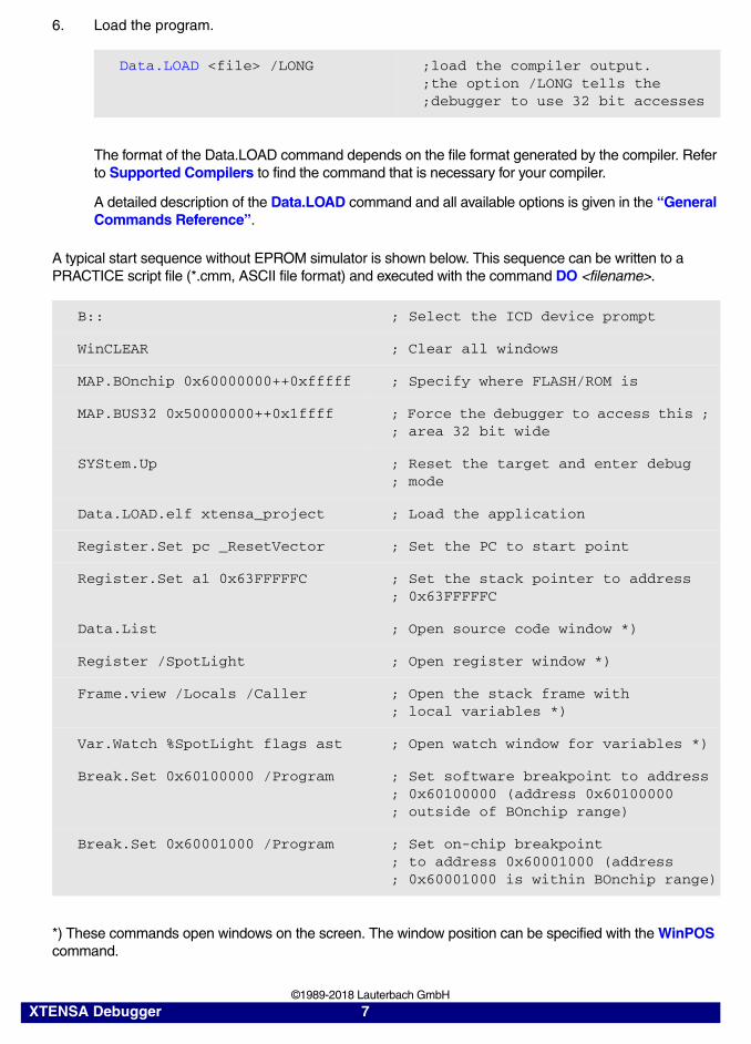
6. Load the program.
The format of the Data.LOAD command depends on the file format generated by the compiler. Refer to Supported Compilers to find the command that is necessary for your compiler.
A detailed description of the Data.LOAD command and all available options is given in the “General Commands Reference”.
A typical start sequence without EPROM simulator is shown below. This sequence can be written to a PRACTICE script file (*.cmm, ASCII file format) and executed with the command DO <filename>.
*) These commands open windows on the screen. The window position can be specified with the WinPOS command.
Data.LOAD <file> /LONG ;load the compiler output.;the option /LONG tells the;debugger to use 32 bit accesses
B:: ; Select the ICD device prompt
WinCLEAR ; Clear all windows
MAP.BOnchip 0x60000000++0xfffff ; Specify where FLASH/ROM is
MAP.BUS32 0x50000000++0x1ffff ; Force the debugger to access this ; ; area 32 bit wide
SYStem.Up ; Reset the target and enter debug; mode
Data.LOAD.elf xtensa_project ; Load the application
Register.Set pc _ResetVector ; Set the PC to start point
Register.Set a1 0x63FFFFFC ; Set the stack pointer to address ; 0x63FFFFFC
Data.List ; Open source code window *)
Register /SpotLight ; Open register window *)
Frame.view /Locals /Caller ; Open the stack frame with ; local variables *)
Var.Watch %SpotLight flags ast ; Open watch window for variables *)
Break.Set 0x60100000 /Program ; Set software breakpoint to address; 0x60100000 (address 0x60100000 ; outside of BOnchip range)
Break.Set 0x60001000 /Program ; Set on-chip breakpoint; to address 0x60001000 (address; 0x60001000 is within BOnchip range)
XTENSA Debugger 7 ©1989-2018 Lauterbach GmbH

Please keep in mind that only the Processor Architecture Manual (the document you are reading at the moment) is CPU specific, while all other parts of the online help are generic for all CPUs. So if there are questions related to the CPU, the Processor Architecture Manual should be your first choice.
NOTE: • Special registers can be viewed in the peripheral file with the command PER <path>\sfr_xt.per. To add your specific registers you can do a copy of this file and modify it using the command: PER.Program <path>\my_sfr_xt.per
• The Register.view window can be resized to view additional registers by pressing on the small field on the right bottom of the window
XTENSA Debugger 8 ©1989-2018 Lauterbach GmbH

Troubleshooting
SYStem.Up Errors
The SYStem.UP command is the first command of a debug session where communication with the target is required. If you receive error messages while executing this command this may have the following reasons.
• The target has no power.
• The target is in reset.
• The XTENSA core is not enabled.
• There is logic added to the JTAG state machine.
• There are additional loads or capacities on the JTAG lines.
• There is a short circuit on at least one of the output lines of the core.
XTENSA Debugger 9 ©1989-2018 Lauterbach GmbH

FAQ
Debugging via VPN
Ref: 0307
The debugger is accessed via Internet/VPN and the performance is very slow. What can be done to improve debug performance?
The main cause for bad debug performance via Internet or VPN are low data throughput and high latency. The ways to improve performance by the debugger are limited:
In PRACTICE scripts, use "SCREEN.OFF" at the beginning of the scriptand "SCREEN.ON" at the end. "SCREEN.OFF" will turn off screenupdates. Please note that if your program stops (e.g. on error) without exe-cuting "SCREEN.OFF", some windows will not be updated.
"SYStem.POLLING SLOW" will set a lower frequency for target statechecks (e.g. power, reset, jtag state). It will take longer for the debugger torecognize that the core stopped on a breakpoint.
"SETUP.URATE 1.s" will set the default update frequency ofData.List/Data.dump/Variable windows to 1 second (the slowest possiblesetting).
prevent unneeded memory accesses using "MAP.UPDATEONCE[address-range]" for RAM and "MAP.CONST [address--range]" forROM/FLASH. Address ranged with "MAP.UPDATEONCE" will read thespecified address range only once after the core stopped at a breakpoint ormanual break. "MAP.CONST" will read the specified address range onlyonce per SYStem.Mode command (e.g. SYStem.Up).
XTENSA Debugger 10 ©1989-2018 Lauterbach GmbH

Setting a Software Breakpoint fails
Ref: 0276
What can be the reasons why setting a software breakpoint fails?
Setting a software breakpoint can fail when the target HW is not able to implement the wanted breakpoint. Possible reasons:
The wanted breakpoint needs special features that are only possible torealize by the trigger unit inside the controller.
Example: Read, write and access (Read/Write) breakpoints ("type" in Break.Set window). Breakpoints with checking in real-time for data-values ("Data"). Breakpoints with special features ("action") like TriggerTrace, TraceEnable, TraceOn/TraceOFF.
TRACE32 can not change the memory.Example: ROM and Flash when no preparation with FLASH.Create, FLASH.TARGET and FLASH.AUTO was made. All type of memory if the memory device is missing the necessary control signals like WriteEnable or settings of registers and SpecialFunctionRegisters (SFR).
Contrary settings in TRACE32.Like: MAP.BOnchip for this memory range. Break.SELect.<breakpoint-type> Onchip (HARD is only available for ICE and FIRE).
RTOS and MMU:If the memory can be changed by Data.Set but the breakpoint doesn't work it might be a problem of using an MMU on target when setting the breakpoint to a symbolic address that is different than the writable and intended memory location.
XTENSA Debugger 11 ©1989-2018 Lauterbach GmbH

XTENSA Specific Implementations
Breakpoints
Software Breakpoints
If a software breakpoint is used, the original code at the breakpoint location is patched by a breakpoint code.
On-chip Breakpoints for Instructions
If on-chip breakpoints are used, the resources to set the breakpoints are provided by the CPU. The parameter NIBREAK of the Debug Option Architectural Addition defines the number of available instruction breakpoints. On-chip breakpoints are usually needed for instructions in FLASH/ROM.
With the command MAP.BOnchip <range> it is possible to tell the debugger where you have ROM / FLASH on the target.
On-chip Breakpoints for Data
To stop the CPU after a read or write access to a memory location on-chip breakpoints are required. The parameter NDBREAK of the Debug Option (Architectural Option of the XTENSA core) defines the number of available data breakpoints.
XTENSA Debugger 12 ©1989-2018 Lauterbach GmbH

Example for Standard Breakpoints
Assume you have a target with NIBREAK=2, NDBREAK=2 and
• FLASH from 0x0--0xfffff
• RAM from 0x100000--0x11ffff
The command to configure TRACE32 correctly for this configuration is:
Map.BOnchip 0x0--0xfffff
The following standard breakpoint combinations are possible.
1. Unlimited breakpoints in RAM and one breakpoint in ROM/FLASH
2. Unlimited breakpoints in RAM and one breakpoint on a read or write access
3. Two breakpoints in ROM/FLASH
4. Two breakpoints on a read or write access
Break.Set 0x100000 /Program ; Software breakpoint 1
Break.Set 0x101000 /Program ; Software breakpoint 2
Break.Set addr /Program ; Software breakpoint 3
Break.Set 0x100 /Program ; On-chip instruction breakpoint
Break.Set 0x100000 /Program ; Software breakpoint 1
Break.Set 0x101000 /Program ; Software breakpoint 2
Break.Set addr /Program ; Software breakpoint 3
Break.Set 0x108000 /Write ; On-chip data breakpoint
Break.Set 0x100 /Program ; On-chip instruction breakpoint 1
Break.Set 0x200 /Program ; On-chip instruction breakpoint 2
Break.Set 0x108000 /Write ; On-chip data breakpoint 1
Break.Set 0x108010 /Read ; On-chip data breakpoint 2
XTENSA Debugger 13 ©1989-2018 Lauterbach GmbH

Runtime Measurement
The command RunTime allows run time measurement based on polling the CPU run status by software. Therefore the result will be about few milliseconds higher than the real value.
XTENSA Debugger 14 ©1989-2018 Lauterbach GmbH

Memory Classes
The following ARM specific memory classes are available.
To access a memory class write the class in front of the address.Example: Data.dump D:0--3
Normally there is no need to use the following memory classes: P, D since program and data memory space are not separated.
MAP.BUS8 Bus width mapping
This command is used to force the debugger to access the specified range with Load / Store 8-bit commands. So if you do a 32 bit wide memory dump (Data.dump <addr> /LONG) the debugger reads byte-by-byte while the window shows the information in 32 bit words.
MAP.BUS16 Bus width mapping
This command is used to force the debugger to access the specified range with Load / Store 16-bit commands. So if you do a 8 bit wide memory dump (Data.dump <addr> /BYTE) the debugger reads word-by-word while the window shows the information byte-by-byte.
As a follow the debugger might read more than the dump window shows, so if a memory cell is sensitive on read accesses you might touch it unintentional.
Memory Class Description
P Program Memory
D Data Memory
VM Virtual Memory (memory on the debug system)
E Run-time memory access(see SYStem.CpuAccess and SYStem.MemAccess)
Format: MAP.BUS8 [<address_range>]
Format: MAP.BUS16 [<address_range>]
XTENSA Debugger 15 ©1989-2018 Lauterbach GmbH

MAP.BUS32 Bus width mapping
This command is used to force the debugger to access the specified range with Load / Store 32-bit commands. So if you do a 8 bit wide memory dump (Data.dump <addr> /BYTE) the debugger reads 32 bit values while the window shows the information byte-by-byte.
As a follow the debugger might read more than the dump window shows, so if a memory cell is sensitive on read accesses you might touch it unintentional.
Format: MAP.BUS32 [<address_range>]
XTENSA Debugger 16 ©1989-2018 Lauterbach GmbH
CPU specific SYStem Commands
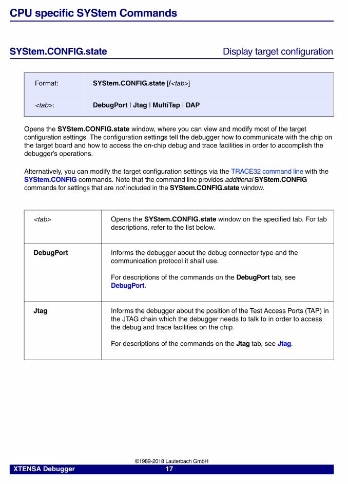
SYStem.CONFIG.state Display target configuration
Opens the SYStem.CONFIG.state window, where you can view and modify most of the target configuration settings. The configuration settings tell the debugger how to communicate with the chip on the target board and how to access the on-chip debug and trace facilities in order to accomplish the debugger’s operations.
Alternatively, you can modify the target configuration settings via the TRACE32 command line with the SYStem.CONFIG commands. Note that the command line provides additional SYStem.CONFIG commands for settings that are not included in the SYStem.CONFIG.state window.
Format: SYStem.CONFIG.state [/<tab>]
<tab>: DebugPort | Jtag | MultiTap | DAP
<tab> Opens the SYStem.CONFIG.state window on the specified tab. For tab descriptions, refer to the list below.
DebugPort Informs the debugger about the debug connector type and the communication protocol it shall use.
For descriptions of the commands on the DebugPort tab, see DebugPort.
Jtag Informs the debugger about the position of the Test Access Ports (TAP) in the JTAG chain which the debugger needs to talk to in order to access the debug and trace facilities on the chip.
For descriptions of the commands on the Jtag tab, see Jtag.
XTENSA Debugger 17 ©1989-2018 Lauterbach GmbH

SYStem.CONFIG Configure debugger according to target topology
MultiTap Informs the debugger about the existence and type of a System/Chip Level Test Access Port. The debugger might need to control it in order to reconfigure the JTAG chain or to control power, clock, reset, and security of different chip components.
For descriptions of the commands on the MultiTap tab, see Multitap.
DAP Informs the debugger about an ARM CoreSight Debug Access Port (DAP) and about how to control the DAP to access chip-internal memory busses (AHB, APB, AXI) or chip-internal JTAG interfaces.
For descriptions of the commands on the DAP tab, see DAP.
Format: SYStem.CONFIG <parameter>SYStem.MultiCore <parameter> (deprecated)
<parameter>:(DebugPort)
CJTAGFLAGS <flags>CJTAGTCA <value>CONNECTOR [MIPI34 | MIPI20T]CORE <core> <chip>CoreNumber <number>DEBUGPORT [DebugCable0 | DebugCableA | DebugCableB]DEBUGPORTTYPE [JTAG | SWD | CJTAG | CJTAGSWD]NIDNTTRSTTORST [ON | OFF]
<parameter>:(DebugPort cont.)
NIDNTPSRISINGEDGE [ON | OFF]NIDNTRSTPOLARITY [High | Low]PortSHaRing [ON | OFF | Auto]Slave [ON | OFF]SWDP [ON | OFF]SWDPIDLEHIGH [ON | OFF]SWDPTargetSel <value>TriState [ON | OFF]
<parameter>:(JTAG)
CHIPDRLENGTH <bits>CHIPDRPATTERN [Standard | Alternate <pattern>]CHIPDRPOST <bits>CHIPDRPRE <bits>CHIPIRLENGTH <bits>CHIPIRPATTERN [Standard | Alternate <pattern>]CHIPIRPOST<bits>CHIPIRPRE <bits>
XTENSA Debugger 18 ©1989-2018 Lauterbach GmbH

<parameter>:(JTAG cont.)
DAP2DRPOST <bits>DAP2DRPRE <bits>DAP2IRPOST <bits>DAP2IRPRE <bits>DAPDRPOST <bits>DAPDRPRE <bits>DAPIRPOST <bits>DAPIRPRE <bits>
<parameter>:(JTAG cont.)
DRPOST <bits>DRPRE <bits>ETBDRPOST <bits>ETBDRPRE <bits>ETBIRPOST <bits>ETBIRPRE <bits>IRPOST<bits>IRPRE <bits>
<parameter>:(JTAG cont.)
NEXTDRPOST <bits>NEXTDRPRE <bits>NEXTIRPOST<bits>NEXTIRPRE <bits>RTPDRPOST <bits>RTPDRPRE <bits>RTPIRPOST <bits>RTPIRPRE <bits>
<parameter>:(JTAG cont.)
Slave [ON | OFF]TAPState <state>TCKLevel <level>TriState [ON | OFF]
<parameter>:(Multitap)
CFGCONNECT <code>DAP2TAP <tap>DAPTAP <tap>DEBUGTAP <tap>ETBTAP <tap>MULTITAP [NONE | IcepickA | IcepickB | IcepickC | IcepickD | IcepickBB | IcepickBC | IcepickCC | IcepickDD | STCLTAP1 | STCLTAP2 | STCLTAP3 | MSMTAP <irlength> <irvalue> <drlength> <drvalue>]NJCR <tap>RTPTAP <tap>SLAVETAP <tap>
XTENSA Debugger 19 ©1989-2018 Lauterbach GmbH

<parameter>:(DAP)
AHBACCESSPORT <port>APBACCESSPORT <port>AXIACCESSPORT <port>COREJTAGPORT <port>DAP2AHBACCESSPORT <port>DAP2APBACCESSPORT <port>DAP2AXIACCESSPORT <port>DAP2COREJTAGPORT <port>
<parameter>:(DAP cont.)
DAP2DEBUGACCESSPORT <port>DAP2JTAGPORT <port>DAP2AHBACCESSPORT <port>DEBUGACCESSPORT <port>JTAGACCESSPORT <port>MEMORYACCESSPORT <port>
<parameter>:(COmponents)
ADTF.Base <address>ADTF.RESETAET.Base <address>AET.RESETBMC.Base <address>BMC.RESETCMI.Base <address>CMI.RESET
<parameter>:(COmponents cont.)
CMI.TraceID <id>COREDEBUG.Base <address>COREDEBUG.RESETCTI.Base <address>CTI.Config [NONE | ARMV1 | ARMPostInit | OMAP3 | TMS570 | CortexV1 | QV1]CTI.RESETDRM.Base <address>DRM.RESET
<parameter>:(COmponents cont.)
DTM.RESETDTM.Type [None | Generic]DWT.Base <address>DWT.RESETEPM.Base <address>EPM.RESETETB2AXI.Base <address>ETB2AXI.RESET
XTENSA Debugger 20 ©1989-2018 Lauterbach GmbH

<parameter>:(COmponents cont.)
ETB.ATBSource <source>ETB.Base <address>ETB.NoFlush [ON | OFF]ETB.RESETETB.Size <size>ETF.ATBSource <source>ETF.Base <address>ETF.RESETETM.Base <address>
<parameter>:(COmponents cont.)
ETM.RESETETR.ATBSource <source>ETR.Base <address>ETR.RESETFUNNEL.ATBSource <sourcelist>FUNNEL.Base <address>FUNNEL.Name <string>FUNNEL.PROGrammable [ON | OFF]
<parameter>:(Components cont.)
FUNNEL.RESETHSM.Base <address>HSM.RESETHTM.Base <address>HTM.RESETHTM.Type [CoreSight | WPT]ICE.Base <address>ICE.RESET
<parameter>:(Components cont.)
ITM.Base <address>ITM.RESETL2CACHE.Base <address>L2CACHE.RESETL2CACHE.Type [NONE | Generic | L210 | L220 | L2C-310 | AURORA | AURORA2]OCP.Base <address>OCP.RESETOCP.TraceID <id>
<parameter>:(Components cont.)
OCP.Type <type>PMI.Base <address>PMI.RESETPMI.TraceID <id>RTP.Base <address>RTP.PerBase <address>RTP.RamBase <address>RTP.RESET
XTENSA Debugger 21 ©1989-2018 Lauterbach GmbH

<parameter>:(Components cont.)
SC.Base <address>SC.RESETSC.TraceID <id>STM.Base <address>STM.Mode [NONE | XTIv2 | SDTI | STP | STP64 | STPv2]STM.RESETSTM.Type [None | GenericARM | SDTI | TI]TPIU.ATBSource <source>TPIU.Base <address>TPIU.RESETTPIU.Type [CoreSight | Generic]
<parameter>:(Deprecated)
BMCBASE <address>BYPASS <seq>COREBASE <address> CTIBASE <address> CTICONFIG [NONE | ARMV1 | ARMPostInit | OMAP3 | TMS570 | CortexV1 | QV1]DEBUGBASE <address>DTMCONFIG [ON | OFF]
<parameter>:(Deprecated cont.)
DTMETBFUNNELPORT <port>DTMFUNNEL2PORT <port>DTMFUNNELPORT <port>DTMTPIUFUNNELPORT <port>DWTBASE <address>ETB2AXIBASE <address> ETBBASE <address>
<parameter>:(Deprecated cont.)
ETBFUNNELBASE <address>ETFBASE <address>ETMBASE <address>ETMETBFUNNELPORT <port>ETMFUNNEL2PORT <port>ETMFUNNELPORT <port>ETMTPIUFUNNELPORT <port>FILLDRZERO [ON | OFF]
<parameter>:(Deprecated cont.)
FUNNEL2BASE <address>FUNNELBASE <address>HSMBASE <address>HTMBASE <address>HTMETBFUNNELPORT <port>HTMFUNNEL2PORT <port>HTMFUNNELPORT <port>HTMTPIUFUNNELPORT <port>
XTENSA Debugger 22 ©1989-2018 Lauterbach GmbH

The SYStem.CONFIG commands inform the debugger about the available on-chip debug and trace components and how to access them.
This is a common description of the SYStem.CONFIG command group for the ARM, CevaX, TI DSP and Hexagon debugger. Each debugger will provide only a subset of these commands. Some commands need a certain CPU type selection (SYStem.CPU <type>) to become active and it might additionally depend on further settings.
Ideally you can select with SYStem.CPU the chip you are using which causes all setup you need and you do not need any further SYStem.CONFIG command.
The SYStem.CONFIG command information shall be provided after the SYStem.CPU command which might be a precondition to enter certain SYStem.CONFIG commands and before you start up the debug session e.g. by SYStem.Up.
<parameter>:(Deprecated cont.)
ITMBASE <address>ITMETBFUNNELPORT <port>ITMFUNNEL2PORT <port>ITMFUNNELPORT <port>ITMTPIUFUNNELPORT <port>PERBASE <address>RAMBASE <address>RTPBASE <address>
<parameter>:(Deprecated cont.)
SDTIBASE <address>STMBASE <address>STMETBFUNNELPORT<port>STMFUNNEL2PORT<port>STMFUNNELPORT<port>STMTPIUFUNNELPORT<port>TIADTFBASE <address>TIDRMBASE <address>
<parameter>:(Deprecated cont.)
TIEPMBASE <address>TIICEBASE <address>TIOCPBASE <address>TIOCPTYPE <type>TIPMIBASE <address>TISCBASE <address>TISTMBASE <address>
<parameter>:(Deprecated cont.)
TPIUBASE <address>TPIUFUNNELBASE <address>TRACEETBFUNNELPORT <port>TRACEFUNNELPORT<port>TRACETPIUFUNNELPORT <port>view
XTENSA Debugger 23 ©1989-2018 Lauterbach GmbH

Syntax remarks:
The commands are not case sensitive. Capital letters show how the command can be shortened.Example: “SYStem.CONFIG.DWT.Base 0x1000” -> “SYS.CONFIG.DWT.B 0x1000”
The dots after “SYStem.CONFIG” can alternatively be a blank.Example: “SYStem.CONFIG.DWT.Base 0x1000” or “SYStem.CONFIG DWT Base 0x1000”.
XTENSA Debugger 24 ©1989-2018 Lauterbach GmbH

<parameters> describing the “DebugPort”
CJTAGFLAGS <flags> Activates bug fixes for “cJTAG” implementations.Bit 0: Disable scanning of cJTAG ID.Bit 1: Target has no “keeper”.Bit 2: Inverted meaning of SREDGE register.Bit 3: Old command opcodes.Bit 4: Unlock cJTAG via APFC register.
Default: 0
CJTAGTCA <value> Selects the TCA (TAP Controller Address) to address a device in a cJTAG Star-2 configuration. The Star-2 configuration requires a unique TCA for each device on the debug port.
CONNECTOR[MIPI34 | MIPI20T]
Specifies the connector “MIPI34” or “MIPI20T” on the target. This is mainly needed in order to notify the trace pin location.
Default: MIPI34 if CombiProbe is used, MIPI20T if uTrace is used.
CORE <core> <chip> The command helps to identify debug and trace resources which are commonly used by different cores. The command might be required in a multicore environment if you use multiple debugger instances (multiple TRACE32 GUIs) to simultaneously debug different cores on the same target system.
Because of the default setting of this command
debugger#1: <core>=1 <chip>=1debugger#2: <core>=1 <chip>=2...
each debugger instance assumes that all notified debug and trace resources can exclusively be used.
But some target systems have shared resources for different cores. For example a common trace port. The default setting causes that each debugger instance will control the (same) trace port. Sometimes it does not hurt if such a module will be controlled twice. So even then it might work. But the correct specification which might be a must is to tell the debugger that these cores sharing resources are on the same <chip>. Whereby the “chip” does not need to be identical with the device on your target board:
debugger#1: <core>=1 <chip>=1debugger#2: <core>=2 <chip>=1
XTENSA Debugger 25 ©1989-2018 Lauterbach GmbH

CORE <core> <chip>
(cont.)
For cores on the same <chip> the debugger assumes they share the same resource if the control registers of the resource has the same address.
Default:<core> depends on CPU selection, usually 1.<chip> derived from CORE= parameter in the configuration file (config.t32), usually 1. If you start multiple debugger instances with the help of t32start.exe you will get ascending values (1, 2, 3,...).
CoreNumber <number> Number of cores to be considered in an SMP (symmetric multiprocessing) debug session. There are core types like ARM11MPCore, CortexA5MPCore, CortexA9MPCore and Scorpion which can be used as a single core processor or as a scalable multicore processor of the same type. If you intend to debug more than one such core in an SMP debug session you need to specify the number of cores you intend to debug.
Default: 1.
DEBUGPORT [DebugCable0 | DebugCa-bleA | DebugCableB]
It specifies which probe cable shall be used e.g. “DebugCableA” or “DebugCableB”. At the moment only the CombiProbe allows to connect more than one probe cable.
Default: depends on detection.
DEBUGPORTTYPE[JTAG | SWD | CJTAG | CJTAGSWD]
It specifies the used debug port type “JTAG”, “SWD”, “CJTAG”, “CJTAG-SWD”. It assumes the selected type is supported by the target.
Default: JTAG.
What is NIDnT?
NIDnT is an acronym for “Narrow Interface for Debug and Test”. NIDnT is a standard from the MIPI Alliance, which defines how to reuse the pins of an existing interface (like for example a microSD card interface) as a debug and test interface.
To support the NIDnT standard in different implementations, TRACE32 has several special options:
XTENSA Debugger 26 ©1989-2018 Lauterbach GmbH

NIDNTPSRISINGEDGE[ON | OFF]
Send data on rising edge for NIDnT PS switching.
NIDnT specifies how to switch, for example, the microSD card interface to a debug interface by sending in a special bit sequence via two pins of the microSD card.
TRACE32 will send the bits of the sequence incident to the falling edge of the clock, because TRACE32 expects that the target samples the bits on the rising edge of the clock.
Some targets will sample the bits on the falling edge of the clock instead. To support such targets, you can configure TRACE32 to send bits on the rising edge of the clock by using SYStem.CONFIG NIDNTPSRISINGEDGE ON
NOTE: Only enable this option right before you send the NIDnT switching bit sequence.Make sure to DISABLE this option, before you try to connect to the target system with for example SYStem.Up.
NIDNTRSTPOLARITY[High | Low]
Usually TRACE32 requires that the system reset line of a target system is low active and has a pull-up on the target system.
When connecting via NIDnT to a target system, the reset line might be a high-active signal.To configure TRACE32 to use a high-active reset signal, useSYStem.CONFIG NIDNTRSTPOLARITY High
This option must be used together withSYStem.CONFIG NIDNTTRSTTORST ONbecause you also have to use the TRST signal of an ARM debug cable as reset signal for NIDnT in this case.
NIDNTTRSTTORST[ON | OFF]
Usually TRACE32 requires that the system reset line of a target system is low active and has a pull-up on the target system.This is how the system reset line is usually implemented on regular ARM-based targets.
When connecting via NIDnT (e.g. a microSD card slot) to the target system, the reset line might not include a pull-up on the target system.To circumvent problems, TRACE32 allows to drive the target reset line via the TRST signal of an ARM debug cable.
Enable this option if you want to use the TRST signal of an ARM debug cable as reset signal for a NIDnT.
XTENSA Debugger 27 ©1989-2018 Lauterbach GmbH
PortSHaRing [ON | OFF | Auto]
Configure if the debug port is shared with another tool, e.g. an ETAS ETK.
OFF: Default. Communicate with the target without sending requests.
ON: Request for access to the debug port and wait until the access is granted before communicating with the target.
Auto: Automatically detect a connected tool on next SYStem.Mode Up, SYStem.Mode Attach or SYStem.Mode Go. If a tool is detected switch to mode ON else switch to mode OFF.
The current setting can be obtained by the PORTSHARING() function, immediate detection can be performed using SYStem.DETECT PortSHaRing.
Slave [ON | OFF] If several debuggers share the same debug port, all except one must have this option active.
JTAG: Only one debugger - the “master” - is allowed to control the signals nTRST and nSRST (nRESET). The other debuggers need to have the setting Slave OFF.
Default: OFF.Default: ON if CORE=... >1 in the configuration file (e.g. config.t32).
SWDP [ON | OFF] With this command you can change from the normal JTAG interface to the serial wire debug mode. SWDP (Serial Wire Debug Port) uses just two signals instead of five. It is required that the target and the debugger hard- and software supports this interface.
Default: OFF.
SWDPIdleHigh [ON | OFF]
Keep SWDIO line high when idle. Only for Serialwire Debug mode. Usually the debugger will pull the SWDIO data line low, when no operation is in progress, so while the clock on the SWCLK line is stopped (kept low).
You can configure the debugger to pull the SWDIO data linehigh, when no operation is in progress by using SYStem.CONFIG SWDPIDLEHIGH ON
Default: OFF.
XTENSA Debugger 28 ©1989-2018 Lauterbach GmbH

SWDPTargetSel <value> Device address in case of a multidrop serial wire debug port.
Default: 0.
TriState [ON | OFF] TriState has to be used if several debug cables are connected to a common JTAG port. TAPState and TCKLevel define the TAP state and TCK level which is selected when the debugger switches to tristate mode. Please note: • nTRST must have a pull-up resistor on the target.• TCK can have a pull-up or pull-down resistor.• Other trigger inputs need to be kept in inactive state.
Default: OFF.
XTENSA Debugger 29 ©1989-2018 Lauterbach GmbH

<parameters> describing the “JTAG” scan chain and signal behavior
With the JTAG interface you can access a Test Access Port controller (TAP) which has implemented a state machine to provide a mechanism to read and write data to an Instruction Register (IR) and a Data Register (DR) in the TAP. The JTAG interface will be controlled by 5 signals: nTRST(reset), TCK (clock), TMS (state machine control), TDI (data input), TDO (data output). Multiple TAPs can be controlled by one JTAG interface by daisy-chaining the TAPs (serial connection). If you want to talk to one TAP in the chain you need to send a BYPASS pattern (all ones) to all other TAPs. For this case the debugger needs to know the position of the TAP it wants to talk to. The TAP position can be defined with the first four commands in the table below.
… DRPOST <bits> Defines the TAP position in a JTAG scan chain. Number of TAPs in the JTAG chain between the TDI signal and the TAP you are describing. In BYPASS mode each TAP contributes one data register bit. See possible TAP types and example below.
Default: 0.
… DRPRE <bits> Defines the TAP position in a JTAG scan chain. Number of TAPs in the JTAG chain between the TAP you are describing and the TDO signal. In BYPASS mode each TAP contributes one data register bit. See possible TAP types and example below.
Default: 0.
… IRPOST <bits> Defines the TAP position in a JTAG scan chain. Number of Instruction Register (IR) bits of all TAPs in the JTAG chain between TDI signal and the TAP you are describing. See possible TAP types and example below.
Default: 0.
… IRPRE <bits> Defines the TAP position in a JTAG scan chain. Number of Instruction Register (IR) bits of all TAPs in the JTAG chain between the TAP you are describing and the TDO signal. See possible TAP types and example below.
Default: 0.
CHIPDRLENGTH <bits>
Number of Data Register (DR) bits which needs to get a certain BYPASS pattern.
CHIPDRPATTERN [Standard | Alter-nate <pattern>]
Data Register (DR) pattern which shall be used for BYPASS instead of the standard (1...1) pattern.
CHIPIRLENGTH <bits>
Number of Instruction Register (IR) bits which needs to get a certain BYPASS pattern.
CHIPIRPATTERN [Standard | Alter-nate <pattern>]
Instruction Register (IR) pattern which shall be used for BYPASS instead of the standard pattern.
XTENSA Debugger 30 ©1989-2018 Lauterbach GmbH

Slave [ON | OFF] If several debuggers share the same debug port, all except one must have this option active.
JTAG: Only one debugger - the “master” - is allowed to control the signals nTRST and nSRST (nRESET). The other debuggers need to have the setting Slave OFF.
Default: OFF.Default: ON if CORE=... >1 in the configuration file (e.g. config.t32).For CortexM: Please check also SYStem.Option DISableSOFTRES [ON | OFF]
TAPState <state> This is the state of the TAP controller when the debugger switches to tristate mode. All states of the JTAG TAP controller are selectable.
0 Exit2-DR1 Exit1-DR2 Shift-DR3 Pause-DR4 Select-IR-Scan5 Update-DR6 Capture-DR7 Select-DR-Scan8 Exit2-IR9 Exit1-IR10 Shift-IR11 Pause-IR12 Run-Test/Idle13 Update-IR14 Capture-IR15 Test-Logic-Reset
Default: 7 = Select-DR-Scan.
TCKLevel <level> Level of TCK signal when all debuggers are tristated. Normally defined by a pull-up or pull-down resistor on the target.
Default: 0.
TriState [ON | OFF] TriState has to be used if several debug cables are connected to a common JTAG port. TAPState and TCKLevel define the TAP state and TCK level which is selected when the debugger switches to tristate mode. Please note: • nTRST must have a pull-up resistor on the target.• TCK can have a pull-up or pull-down resistor.• Other trigger inputs need to be kept in inactive state.
Default: OFF.
XTENSA Debugger 31 ©1989-2018 Lauterbach GmbH
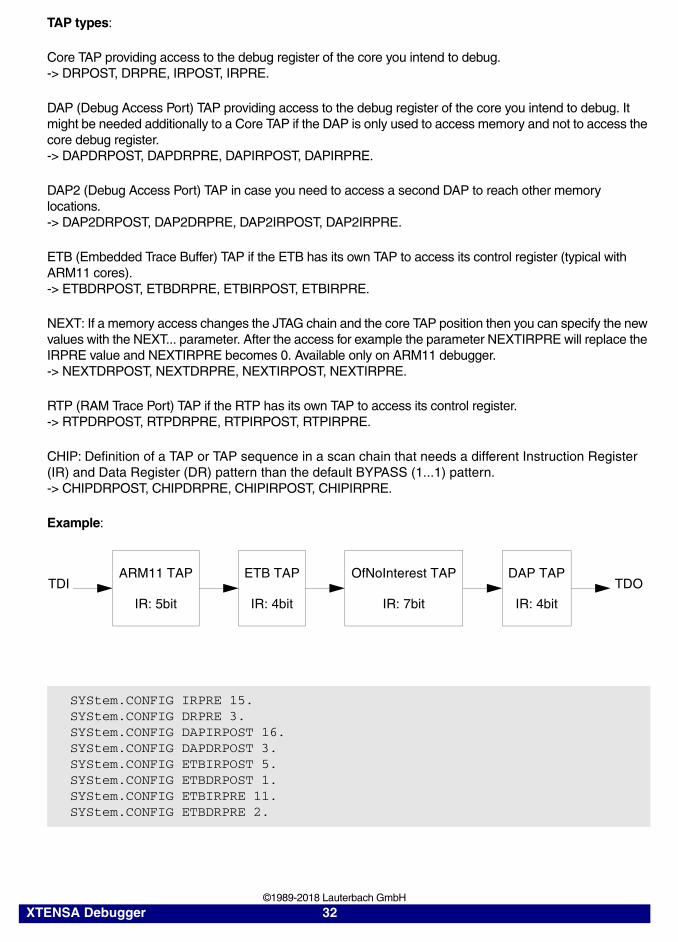
TAP types:
Core TAP providing access to the debug register of the core you intend to debug.-> DRPOST, DRPRE, IRPOST, IRPRE.
DAP (Debug Access Port) TAP providing access to the debug register of the core you intend to debug. It might be needed additionally to a Core TAP if the DAP is only used to access memory and not to access the core debug register.-> DAPDRPOST, DAPDRPRE, DAPIRPOST, DAPIRPRE.
DAP2 (Debug Access Port) TAP in case you need to access a second DAP to reach other memory locations.-> DAP2DRPOST, DAP2DRPRE, DAP2IRPOST, DAP2IRPRE.
ETB (Embedded Trace Buffer) TAP if the ETB has its own TAP to access its control register (typical with ARM11 cores).-> ETBDRPOST, ETBDRPRE, ETBIRPOST, ETBIRPRE.
NEXT: If a memory access changes the JTAG chain and the core TAP position then you can specify the new values with the NEXT... parameter. After the access for example the parameter NEXTIRPRE will replace the IRPRE value and NEXTIRPRE becomes 0. Available only on ARM11 debugger.-> NEXTDRPOST, NEXTDRPRE, NEXTIRPOST, NEXTIRPRE.
RTP (RAM Trace Port) TAP if the RTP has its own TAP to access its control register.-> RTPDRPOST, RTPDRPRE, RTPIRPOST, RTPIRPRE.
CHIP: Definition of a TAP or TAP sequence in a scan chain that needs a different Instruction Register (IR) and Data Register (DR) pattern than the default BYPASS (1...1) pattern.-> CHIPDRPOST, CHIPDRPRE, CHIPIRPOST, CHIPIRPRE.
Example:
SYStem.CONFIG IRPRE 15.SYStem.CONFIG DRPRE 3.SYStem.CONFIG DAPIRPOST 16.SYStem.CONFIG DAPDRPOST 3.SYStem.CONFIG ETBIRPOST 5.SYStem.CONFIG ETBDRPOST 1.SYStem.CONFIG ETBIRPRE 11.SYStem.CONFIG ETBDRPRE 2.
ARM11 TAP
IR: 5bit
ETB TAP
IR: 4bit
DAP TAP
IR: 4bit
TDI TDOOfNoInterest TAP
IR: 7bit
XTENSA Debugger 32 ©1989-2018 Lauterbach GmbH

XTENSA Debugger 33 ©1989-2018 Lauterbach GmbH
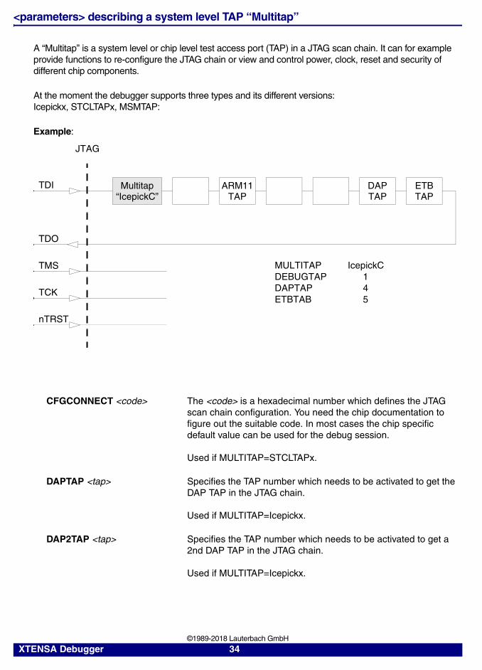
<parameters> describing a system level TAP “Multitap”
A “Multitap” is a system level or chip level test access port (TAP) in a JTAG scan chain. It can for example provide functions to re-configure the JTAG chain or view and control power, clock, reset and security of different chip components.
At the moment the debugger supports three types and its different versions:Icepickx, STCLTAPx, MSMTAP:
Example:
CFGCONNECT <code> The <code> is a hexadecimal number which defines the JTAG scan chain configuration. You need the chip documentation to figure out the suitable code. In most cases the chip specific default value can be used for the debug session.
Used if MULTITAP=STCLTAPx.
DAPTAP <tap> Specifies the TAP number which needs to be activated to get the DAP TAP in the JTAG chain.
Used if MULTITAP=Icepickx.
DAP2TAP <tap> Specifies the TAP number which needs to be activated to get a 2nd DAP TAP in the JTAG chain.
Used if MULTITAP=Icepickx.
TDO
TMS
TCK
nTRST
ARM11TAP
DAPTAP
ETBTAP
MULTITAP IcepickCDEBUGTAPDAPTAPETBTAB
Multitap“IcepickC”
JTAG
145
TDI
XTENSA Debugger 34 ©1989-2018 Lauterbach GmbH

DEBUGTAP <tap> Specifies the TAP number which needs to be activated to get the core TAP in the JTAG chain. E.g. ARM11 TAP if you intend to debug an ARM11.
Used if MULTITAP=Icepickx.
ETBTAP <tap> Specifies the TAP number which needs to be activated to get the ETB TAP in the JTAG chain.
Used if MULTITAP=Icepickx. ETB = Embedded Trace Buffer.
MULTITAP[NONE | IcepickA | IcepickB | IcepickC | IcepickD | IcepickBB | IcepickBC | IcepickCC | IcepickDD | STCLTAP1 | STCLTAP2 | STCLTAP3 | MSMTAP <irlength> <irvalue> <drlength> <drvalue>]
Selects the type and version of the MULTITAP.
In case of MSMTAP you need to add parameters which specify which IR pattern and DR pattern needed to be shifted by the debugger to initialize the MSMTAP. Please note some of these parameters need a decimal input (dot at the end).
IcepickXY means that there is an Icepick version “X” which includes a subsystem with an Icepick of version “Y”.
NJCR <tap> Number of a Non-JTAG Control Register (NJCR) which shall be used by the debugger.
Used if MULTITAP=Icepickx.
RTPTAP <tap> Specifies the TAP number which needs to be activated to get the RTP TAP in the JTAG chain.
Used if MULTITAP=Icepickx. RTP = RAM Trace Port.
SLAVETAP <tap> Specifies the TAP number to get the Icepick of the sub-system in the JTAG scan chain.
Used if MULTITAP=IcepickXY (two Icepicks).
XTENSA Debugger 35 ©1989-2018 Lauterbach GmbH

<parameters> configuring a CoreSight Debug Access Port “DAP”
A Debug Access Port (DAP) is a CoreSight module from ARM which provides access via its debugport (JTAG, cJTAG, SWD) to:
1. Different memory busses (AHB, APB, AXI). This is especially important if the on-chip debug register needs to be accessed this way. You can access the memory buses by using certain access classes with the debugger commands: “AHB:”, “APB:”, “AXI:, “DAP”, “E:”. The interface to these buses is called Memory Access Port (MEM-AP).
2. Other, chip-internal JTAG interfaces. This is especially important if the core you intend to debug is connected to such an internal JTAG interface. The module controlling these JTAG interfaces is called JTAG Access Port (JTAG-AP). Each JTAG-AP can control up to 8 internal JTAG interfaces. A port number between 0 and 7 denotes the JTAG interfaces to be addressed.
3. At emulation or simulation system with using bus transactors the access to the busses must be specified by using the transactor identification name instead using the access port commands. For emulations/simulations with a DAP transactor the individual bus transactor name don’t need to be configured. Instead of this the DAP transactor name need to be passed and the regular access ports to the busses.
XTENSA Debugger 36 ©1989-2018 Lauterbach GmbH

Example:
AHBACCESSPORT <port> DAP access port number (0-255) which shall be used for “AHB:” access class. Default: <port>=0.
APBACCESSPORT <port> DAP access port number (0-255) which shall be used for “APB:” access class. Default: <port>=1.
AXIACCESSPORT <port> DAP access port number (0-255) which shall be used for “AXI:” access class. Default: port not available
COREJTAGPORT <port> JTAG-AP port number (0-7) connected to the core which shall be debugged.
Deb
ug
ger
Memory Access Port(MEM-AP)
1
Memory Access Port(MEM-AP)
0
JTAG Access Port(JTAG-AP)
2S
yste
m B
us (
AH
B)
Deb
ug B
us (
AP
B)
System Memory
Debug Register
Trace Register
ROM Table
0 JTAG
7 JTAG ARM9
Debug Access Port (DAP)
COREJTAGPORT 7AHBACCESSPORT 0MEMORYACCESSPORT 0APBACCESSPORT 1DEBUGACCESSPORT 1JTAGACCESSPORT 2
Debug PortJTAG or cJTAG orSWD
Chip
XTENSA Debugger 37 ©1989-2018 Lauterbach GmbH

DAP2AHBACCESSPORT <port>
DAP2 access port number (0-255) which shall be used for “AHB2:” access class. Default: <port>=0.
DAP2APBACCESSPORT <port>
DAP2 access port number (0-255) which shall be used for “APB2:” access class. Default: <port>=1.
DAP2AXIACCESSPORT <port>
DAP2 access port number (0-255) which shall be used for “AXI2:” access class. Default: port not available
DAP2DEBUGACCESS-PORT <port>
DAP2 access port number (0-255) where the debug register can be found (typically on APB). Used for “DAP2:” access class. Default: <port>=1.
DAP2COREJTAGPORT <port>
JTAG-AP port number (0-7) connected to the core which shall be debugged. The JTAG-AP can be found on another DAP (DAP2).
DAP2JTAGPORT <port> JTAG-AP port number (0-7) for an (other) DAP which is connected to a JTAG-AP.
DAP2MEMORYACCESS-PORT <port>
DAP2 access port number where system memory can be accessed even during runtime (typically on AHB). Used for “E:” access class while running, assuming “SYStem.MemoryAccess DAP2”. Default: <port>=0.
DEBUGACCESSPORT <port>
DAP access port number (0-255) where the debug register can be found (typically on APB). Used for “DAP:” access class. Default: <port>=1.
JTAGACCESSPORT <port> DAP access port number (0-255) of the JTAG Access Port.
MEMORYACCESSPORT <port>
DAP access port number where system memory can be accessed even during runtime (typically on AHB). Used for “E:” access class while running, assuming “SYStem.MemoryAccess DAP”. Default: <port>=0.
AHBNAME <name> AHB bus transactor name that shall be used for “AHB:” access class.
APBNAME <name> APB bus transactor name that shall be used for “APB:” access class.
AXINAME <name> AXI bus transactor name that shall be used for “AXI:” access class.
DAP2AHBNAME <name> AHB bus transactor name that shall be used for “AHB2:” access class.
XTENSA Debugger 38 ©1989-2018 Lauterbach GmbH
DAP2APBNAME <name> APB bus transactor name that shall be used for “APB2:” access class.
DAP2AXINAME <name> AXI bus transactor name that shall be used for “AXI2:” access class.
DAP2DEBUGBUSNAME <name>
APB bus transactor name identifying the bus where the debug register can be found. Used for “DAP2:” access class.
DAP2MEMORYBUSNAME <name>
AHB bus transactor name identifying the bus where system memory can be accessed even during runtime. Used for “E:” access class while running, assuming “SYStem.MemoryAccess DAP2”.
DEBUGBUSNAME <name> APB bus transactor name identifying the bus where the debug register can be found. Used for “DAP:” access class.
MEMORYBUSNAME <name>
AHB bus transactor name identifying the bus where system memory can be accessed even during runtime. Used for “E:” access class while running, assuming “SYStem.MemoryAccess DAP”.
DAPNAME <name> DAP transactor name that shall be used for DAP access ports.
DAP2NAME <name> DAP transactor name that shall be used for DAP access ports of 2nd order.
XTENSA Debugger 39 ©1989-2018 Lauterbach GmbH

<parameters> describing debug and trace “Components”
In the “Components” folder in the “SYStem.CONFIG.state” window you can comfortably add the debug and trace components your chip includes and which you intend to use with the debugger’s help.
Each configuration can be done by a command in a script file as well. Then you do not need to enter everything again on the next debug session. If you press the button with the three dots you get the corresponding command in the command line where you can view and maybe copy it into a script file.
XTENSA Debugger 40 ©1989-2018 Lauterbach GmbH

You can have several of the following components: CMI, ETB, ETF, ETR, FUNNEL, STM.Example: FUNNEL1, FUNNEL2, FUNNEL3,...
The <address> parameter can be just an address (e.g. 0x80001000) or you can add the access class in front (e.g. AHB:0x80001000). Without access class it gets the command specific default access class which is “EDAP:” in most cases.
Example:
SYStem.CONFIG.COREDEBUG.Base 0x80010000 0x80012000SYStem.CONFIG.BMC.Base 0x80011000 0x80013000SYStem.CONFIG.ETM.Base 0x8001c000 0x8001d000SYStem.CONFIG.STM1.Base EAHB:0x20008000SYStem.CONFIG.STM1.Type ARMSYStem.CONFIG.STM1.Mode STPv2SYStem.CONFIG.FUNNEL1.Base 0x80004000SYStem.CONFIG.FUNNEL2.Base 0x80005000SYStem.CONFIG.TPIU.Base 0x80003000SYStem.CONFIG.FUNNEL1.ATBSource ETM.0 0 ETM.1 1SYStem.CONFIG.FUNNEL2.ATBSource FUNNEL1 0 STM1 7SYStem.CONFIG.TPIU.ATBSource FUNNEL2
ETM
ETM
STM
Core
Core
FUNNEL
TPIUFUNNEL
0
10
7
XTENSA Debugger 41 ©1989-2018 Lauterbach GmbH

… .ATBSource <source> Specify for components collecting trace information from where the trace data are coming from. This way you inform the debugger about the interconnection of different trace components on a common trace bus.
You need to specify the “... .Base <address>” or other attributes that define the amount of existing peripheral modules before you can describe the interconnection by “... .ATBSource <source>”.
A CoreSight trace FUNNEL has eight input ports (port 0-7) to combine the data of various trace sources to a common trace stream. Therefore you can enter instead of a single source a list of sources and input port numbers.
Example:SYStem.CONFIG FUNNEL.ATBSource ETM 0 HTM 1 STM 7
Meaning: The funnel gets trace data from ETM on port 0, from HTM on port 1 and from STM on port 7.
In an SMP (Symmetric MultiProcessing) debug session where you used a list of base addresses to specify one component per core you need to indicate which component in the list is meant:
XTENSA Debugger 42 ©1989-2018 Lauterbach GmbH

Example: Four cores with ETM modules.SYStem.CONFIG ETM.Base 0x1000 0x2000 0x3000 0x4000SYStem.CONFIG FUNNEL1.ATBSource ETM.0 0 ETM.1 1 ETM.2 2 ETM.3 3"...2" of "ETM.2" indicates it is the third ETM module which has the base address 0x3000. The indices of a list are 0, 1, 2, 3,... If the numbering is accelerating, starting from 0, without gaps, like the example above then you can shorten it to SYStem.CONFIG FUNNEL1.ATBSource ETM
Example: Four cores, each having an ETM module and an ETB module.SYStem.CONFIG ETM.Base 0x1000 0x2000 0x3000 0x4000SYStem.CONFIG ETB.Base 0x5000 0x6000 0x7000 0x8000SYStem.CONFIG ETB.ATBSource ETM.2 2The third "ETM.2" module is connected to the third ETB. The last "2" in the command above is the index for the ETB. It is not a port number which exists only for FUNNELs.
For a list of possible components including a short description see Components and available commands.
… .BASE <address> This command informs the debugger about the start address of the register block of the component. And this way it notifies the existence of the component. An on-chip debug and trace component typically provides a control register block which needs to be accessed by the debugger to control this component.
Example: SYStem.CONFIG ETMBASE APB:0x8011c000
Meaning: The control register block of the Embedded Trace Macrocell (ETM) starts at address 0x8011c000 and is accessible via APB bus.
In an SMP (Symmetric MultiProcessing) debug session you can enter for the components BMC, COREBEBUG, CTI, ETB, ETF, ETM, ETR a list of base addresses to specify one component per core.
Example assuming four cores: SYStem.CONFIG COREDEBUG.Base 0x80001000 0x80003000 0x80005000 0x80007000
For a list of possible components including a short description see Components and available commands.
… .RESET Undo the configuration for this component. This does not cause a physical reset for the component on the chip.
For a list of possible components including a short description see Components and available commands.
XTENSA Debugger 43 ©1989-2018 Lauterbach GmbH

… .TraceID <id> Identifies from which component the trace packet is coming from. Components which produce trace information (trace sources) for a common trace stream have a selectable “.TraceID <id>”.
If you miss this SYStem.CONFIG command for a certain trace source (e.g. ETM) then there is a dedicated command group for this component where you can select the ID (ETM.TraceID <id>).
The default setting is typically fine because the debugger uses different default trace IDs for different components.
For a list of possible components including a short description see Components and available commands.
CTI.Config <type> Informs about the interconnection of the core Cross Trigger Interfaces (CTI). Certain ways of interconnection are common and these are supported by the debugger e.g. to cause a synchronous halt of multiple cores.
NONE: The CTI is not used by the debugger.ARMV1: This mode is used for ARM7/9/11 cores which support synchronous halt, only.ARMPostInit: Like ARMV1 but the CTI connection differs from the ARM recommendation. OMAP3: This mode is not yet used.TMS570: Used for a certain CTI connection used on a TMS570 derivative.CortexV1: The CTI will be configured for synchronous start and stop via CTI. It assumes the connection of DBGRQ, DBGACK, DBGRESTART signals to CTI are done as recommended by ARM. The CTIBASE must be notified. “CortexV1” is the default value if a Cortex-A/R core is selected and the CTIBASE is notified.QV1: This mode is not yet used.
ARMV8V1: Channel 0 and 1 of the CTM are used to distribute start/stop events from and to the CTIs. ARMv8 only.ARMV8V2: Channel 2 and 3 of the CTM are used to distribute start/stop events from and to the CTIs. ARMv8 only.
DTM.Type [None | Generic] Informs the debugger that a customer proprietary Data Trace Message (DTM) module is available. This causes the debugger to consider this source when capturing common trace data. Trace data from this module will be recorded and can be accessed later but the unknown DTM module itself will not be controlled by the debugger.
ETB.NoFlush [ON | OFF] Deactivates an ETB flush request at the end of the trace recording. This is a workaround for a bug on a certain chip. You will loose trace data at the end of the recording. Don’t use it if not needed. Default: OFF.
XTENSA Debugger 44 ©1989-2018 Lauterbach GmbH
ETB.Size <size> Specifies the size of the Embedded Trace Buffer. The ETB size can normally be read out by the debugger. Therefore this command is only needed if this can not be done for any reason.
ETM.StackMode [NotAvail-bale | TRGETM | FULLTIDRM | NOTSET | FULLSTOP | FULLCTI]
Specifies the which method is used to implement the Stack mode of the on-chip trace.NotAvailable: stack mode is not available for this on-chip trace.TRGETM: the trigger delay counter of the onchip-trace is used. It starts by a trigger signal that must be provided by a trace source. Usually those events are routed through one or more CTIs to the on-chip trace.FULLTIDRM: trigger mechanism for TI devices.NOTSET: the method is derived by other GUIs or hardware. detection.FULLSTOP: on-chip trace stack mode by implementation.FULLCTI: on-chip trace provides a trigger signal that is routed back to on-chip trace over a CTI.
FUNNEL.Name <string> It is possible that different funnels have the same address for their control register block. This assumes they are on different buses and for different cores. In this case it is needed to give the funnel different names to differentiate them.
FUNNEL.PROGrammable [ON | OFF]
IIn case the funnel can not or may not be programmed by the debugger, this option needs to be OFF. Default is ON.
HTM.Type [CoreSight | WPT] Selects the type of the AMBA AHB Trace Macrocell (HTM).CoreSight is the type as described in the ARM CoreSight manuals. WPT is a NXP proprietary trace module.
L2CACHE.Type [NONE | Generic | L210 | L220 | L2C-310 | AURORA | AURORA2]
Selects the type of the level2 cache controller. L210, L220, L2C-310 are controller types provided by ARM. AURORAx are Marvell types. The ‘Generic’ type does not need certain treatment by the debugger.
OCP.Type <type> Specifies the type of the OCP module. The <type> is just a number which you need to figure out in the chip documentation.
RTP.PerBase <address> PERBASE specifies the base address of the core peripheral registers which accesses shall be traced. PERBASE is needed for the RAM Trace Port (RTP) which is available on some derivatives from Texas Instruments. The trace packages include only relative addresses to PERBASE and RAMBASE.
RTP.RamBase <address> RAMBASE is the start address of RAM which accesses shall be traced. RAMBASE is needed for the RAM Trace Port (RTP) which is available on some derivatives from Texas Instruments. The trace packages include only relative addresses to PERBASE and RAMBASE.
STM.Mode [NONE | XTIv2 | SDTI | STP | STP64 | STPv2]
Selects the protocol type used by the System Trace Module (STM).
XTENSA Debugger 45 ©1989-2018 Lauterbach GmbH

Components and available commands
See the description of the commands above. Please note that there is a common description for ... .ATBSource, ... .Base, , ... .RESET, ... .TraceID.
ADTF.Base <address>ADTF.RESETAMBA trace bus DSP Trace Formatter (ADTF) - Texas InstrumentsModule of a TMS320C5x or TMS320C6x core converting program and data trace information in ARM CoreSight compliant format.
AET.Base <address>AET.RESETAdvanced Event Triggering unit (AET) - Texas InstrumentsTrace source module of a TMS320C5x or TMS320C6x core delivering program and data trace information.
BMC.Base <address>BMC.RESETPerformance Monitor Unit (PMU) - ARM debug module, e.g. on Cortex-A/RBench-Mark-Counter (BMC) is the TRACE32 term for the same thing.The module contains counter which can be programmed to count certain events (e.g. cache hits).
CMI.Base <address>CMI.RESETCMI.TraceID <id>Clock Management Instrumentation (CMI) - Texas InstrumentsTrace source delivering information about clock status and events to a system trace module.
COREDEBUG.Base <address>COREDEBUG.RESETCore Debug Register - ARM debug register, e.g. on Cortex-A/RSome cores do not have a fix location for their debug register used to control the core. In this case it is essential to specify its location before you can connect by e.g. SYStem.Up.
STM.Type [None | Generic | ARM | SDTI | TI]
Selects the type of the System Trace Module (STM). Some types allow to work with different protocols (see STM.Mode).
TPIU.Type [CoreSight | Generic]
Selects the type of the Trace Port Interface Unit (TPIU).
CoreSight: Default. CoreSight TPIU. TPIU control register located at TPIU.Base <address> will be handled by the debugger.
Generic: Proprietary TPIU. TPIU control register will not be handled by the debugger.
XTENSA Debugger 46 ©1989-2018 Lauterbach GmbH

CTI.Base <address>CTI.Config [NONE | ARMV1 | ARMPostInit | OMAP3 | TMS570 | CortexV1 | QV1]CTI.RESETCross Trigger Interface (CTI) - ARM CoreSight moduleIf notified the debugger uses it to synchronously halt (and sometimes also to start) multiple cores.
DRM.Base <address>DRM.RESETDebug Resource Manager (DRM) - Texas InstrumentsIt will be used to prepare chip pins for trace output.
DTM.RESETDTM.Type [None | Generic]Data Trace Module (DTM) - generic, CoreSight compliant trace source moduleIf specified it will be considered in trace recording and trace data can be accessed afterwards.DTM module itself will not be controlled by the debugger.
DWT.Base <address>DWT.RESETData Watchpoint and Trace unit (DWT) - ARM debug module on Cortex-M coresNormally fix address at 0xE0001000 (default).
EPM.Base <address>EPM.RESETEmulation Pin Manager (EPM) - Texas InstrumentsIt will be used to prepare chip pins for trace output.
ETB2AXI.Base <address>ETB2AXI.RESETETB to AXI moduleSimilar to an ETR.
ETB.ATBSource <source>ETB.Base <address>ETB.RESETETB.Size <size>Embedded Trace Buffer (ETB) - ARM CoreSight moduleEnables trace to be stored in a dedicated SRAM. The trace data will be read out through the debug port after the capturing has finished.
ETF.ATBSource <source>ETF.Base <address>ETF.RESETEmbedded Trace FIFO (ETF) - ARM CoreSight moduleOn-chip trace buffer used to lower the trace bandwidth peaks.
ETM.Base <address>ETM.RESETEmbedded Trace Macrocell (ETM) - ARM CoreSight moduleProgram Trace Macrocell (PTM) - ARM CoreSight moduleTrace source providing information about program flow and data accesses of a core.The ETM commands will be used even for PTM.
XTENSA Debugger 47 ©1989-2018 Lauterbach GmbH

ETR.ATBSource <source>ETR.Base <address>ETR.RESETEmbedded Trace Router (ETR) - ARM CoreSight moduleEnables trace to be routed over an AXI bus to system memory or to any other AXI slave.
FUNNEL.ATBSource <sourcelist>FUNNEL.Base <address>FUNNEL.Name <string>FUNNEL.PROGrammable [ON | OFF]FUNNEL.RESETCoreSight Trace Funnel (CSTF) - ARM CoreSight moduleCombines multiple trace sources onto a single trace bus (ATB = AMBA Trace Bus)
HSM.Base <address>HSM.RESETHardware Security Module (HSM) - Infineon
HTM.Base <address>HTM.RESETHTM.Type [CoreSight | WPT]AMBA AHB Trace Macrocell (HTM) - ARM CoreSight moduleTrace source delivering trace data of access to an AHB bus.
ICE.Base <address>ICE.RESETICE-Crusher (ICE) - Texas Instruments
ITM.Base <address>ITM.RESETInstrumentation Trace Macrocell (ITM) - ARM CoreSight moduleTrace source delivering system trace information e.g. sent by software in printf() style.
L2CACHE.Base <address>L2CACHE.RESETL2CACHE.Type [NONE | Generic | L210 | L220 | L2C-310 | AURORA | AURORA2]Level 2 Cache ControllerThe debugger might need to handle the controller to ensure cache coherency for debugger operation.
OCP.Base <address>OCP.RESETOCP.TraceID <id>OCP.Type <type>Open Core Protocol watchpoint unit (OCP) - Texas InstrumentsTrace source module delivering bus trace information to a system trace module.
PMI.Base <address>PMI.RESETPMI.TraceID <id>Power Management Instrumentation (PMI) - Texas InstrumentsTrace source reporting power management events to a system trace module.
XTENSA Debugger 48 ©1989-2018 Lauterbach GmbH
RTP.Base <address>RTP.PerBase <address>RTP.RamBase <address>RTP.RESETRAM Trace Port (RTP) - Texas InstrumentsTrace source delivering trace data about memory interface usage.
SC.Base <address>SC.RESETSC.TraceID <id>Statistic Collector (SC) - Texas InstrumentsTrace source delivering statistic data about bus traffic to a system trace module.
STM.Base <address>STM.Mode [NONE | XTIv2 | SDTI | STP | STP64 | STPv2]STM.RESETSTM.Type [None | Generic | ARM | SDTI | TI]System Trace Macrocell (STM) - MIPI, ARM CoreSight, othersTrace source delivering system trace information e.g. sent by software in printf() style.
TPIU.ATBSource <source>TPIU.Base <address>TPIU.RESETTPIU.Type [CoreSight | Generic]Trace Port Interface Unit (TPIU) - ARM CoreSight moduleTrace sink sending the trace off-chip on a parallel trace port (chip pins).
XTENSA Debugger 49 ©1989-2018 Lauterbach GmbH

<parameters> which are “Deprecated”
In the last years the chips and its debug and trace architecture became much more complex. Especially the CoreSight trace components and their interconnection on a common trace bus required a reform of our commands. The new commands can deal even with complex structures.
… BASE <address> This command informs the debugger about the start address of the register block of the component. And this way it notifies the existence of the component. An on-chip debug and trace component typically provides a control register block which needs to be accessed by the debugger to control this component.
Example: SYStem.CONFIG ETMBASE APB:0x8011c000
Meaning: The control register block of the Embedded Trace Macrocell (ETM) starts at address 0x8011c000 and is accessible via APB bus.
In an SMP (Symmetric MultiProcessing) debug session you can enter for the components BMC, CORE, CTI, ETB, ETF, ETM, ETR a list of base addresses to specify one component per core.
Example assuming four cores: “SYStem.CONFIG COREBASE 0x80001000 0x80003000 0x80005000 0x80007000”.
COREBASE (old syntax: DEBUGBASE): Some cores e.g. Cortex-A or Cortex-R do not have a fix location for their debug register which are used for example to halt and start the core. In this case it is essential to specify its location before you can connect by e.g. SYStem.Up.
PERBASE and RAMBASE are needed for the RAM Trace Port (RTP) which is available on some derivatives from Texas Instruments. PERBASE specifies the base address of the core peripheral registers which accesses shall be traced, RAMBASE is the start address of RAM which accesses shall be traced. The trace packages include only relative addresses to PERBASE and RAMBASE.
For a list of possible components including a short description see Components and available commands.
XTENSA Debugger 50 ©1989-2018 Lauterbach GmbH

… PORT <port> Informs the debugger about which trace source is connected to which input port of which funnel. A CoreSight trace funnel provides 8 input ports (port 0-7) to combine the data of various trace sources to a common trace stream.
Example: SYStem.CONFIG STMFUNNEL2PORT 3
Meaning: The System Trace Module (STM) is connected to input port #3 on FUNNEL2.
On an SMP debug session some of these commands can have a list of <port> parameter.
In case there are dedicated funnels for the ETB and the TPIU their base addresses are specified by ETBFUNNELBASE, TPIUFUNNELBASE respectively. And the funnel port number for the ETM are declared by ETMETBFUNNELPORT, ETMTPIUFUNNELPORT respectively.
TRACE... stands for the ADTF trace source module.
For a list of possible components including a short description see Components and available commands.
BYPASS <seq> With this option it is possible to change the JTAG bypass instruction pattern for other TAPs. It works in a multi-TAP JTAG chain for the IRPOST pattern, only, and is limited to 64 bit. The specified pattern (hexadecimal) will be shifted least significant bit first. If no BYPASS option is used, the default value is “1” for all bits.
CTICONFIG <type> Informs about the interconnection of the core Cross Trigger Interfaces (CTI). Certain ways of interconnection are common and these are supported by the debugger e.g. to cause a synchronous halt of multiple cores.
NONE: The CTI is not used by the debugger.ARMV1: This mode is used for ARM7/9/11 cores which support synchronous halt, only.ARMPostInit: Like ARMV1 but the CTI connection differs from the ARM recommendation. OMAP3: This mode is not yet used.TMS570: Used for a certain CTI connection used on a TMS570 derivative.CortexV1: The CTI will be configured for synchronous start and stop via CTI. It assumes the connection of DBGRQ, DBGACK, DBGRESTART signals to CTI are done as recommended by ARM. The CTIBASE must be notified. “CortexV1” is the default value if a Cortex-A/R core is selected and the CTIBASE is notified.QV1: This mode is not yet used.
XTENSA Debugger 51 ©1989-2018 Lauterbach GmbH

Deprecated versa new command
In the following you find the list of deprecated commands which can still be used for compatibility reasons and the corresponding new command.
SYStem.CONFIG <parameter>
DTMCONFIG [ON | OFF] Informs the debugger that a customer proprietary Data Trace Message (DTM) module is available. This causes the debugger to consider this source when capturing common trace data. Trace data from this module will be recorded and can be accessed later but the unknown DTM module itself will not be controlled by the debugger.
FILLDRZERO [ON | OFF] This changes the bypass data pattern for other TAPs in a multi-TAP JTAG chain. It changes the pattern from all “1” to all “0”. This is a workaround for a certain chip problem. It is available on the ARM9 debugger, only.
TIOCPTYPE <type> Specifies the type of the OCP module from Texas Instruments (TI).
view Opens a window showing most of the SYStem.CONFIG settings and allows to modify them.
<parameter>:(Deprecated)
<parameter>:(New)
BMCBASE <address> BMC.Base <address>
BYPASS <seq> CHIPIRPRE <bits>CHIPIRLENGTH <bits>CHIPIRPATTERN.Alternate <pattern>
COREBASE <address> COREDEBUG.Base <address>
CTIBASE <address> CTI.Base <address>
CTICONFIG <type> CTI.Config <type>
DEBUGBASE <address> COREDEBUG.Base <address>
DTMCONFIG [ON | OFF] DTM.Type.Generic
DTMETBFUNNELPORT <port> FUNNEL4.ATBSource DTM <port> (1)
DTMFUNNEL2PORT <port> FUNNEL2.ATBSource DTM <port> (1)
DTMFUNNELPORT <port> FUNNEL1.ATBSource DTM <port> (1)
DTMTPIUFUNNELPORT <port> FUNNEL3.ATBSource DTM <port> (1)
DWTBASE <address> DWT.Base <address>
ETB2AXIBASE <address> ETB2AXI.Base <address>
XTENSA Debugger 52 ©1989-2018 Lauterbach GmbH
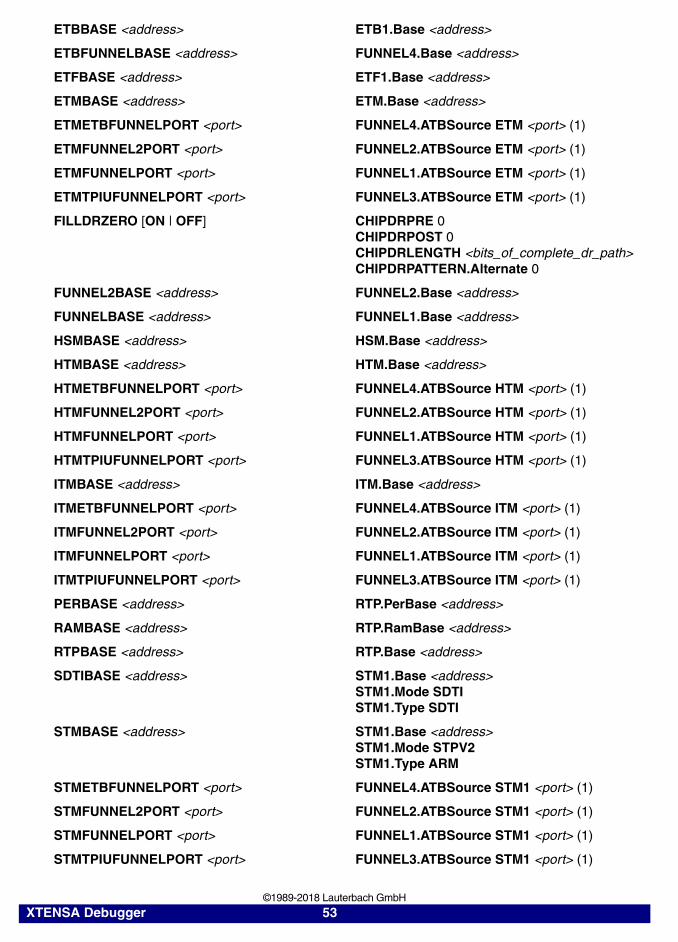
ETBBASE <address> ETB1.Base <address>
ETBFUNNELBASE <address> FUNNEL4.Base <address>
ETFBASE <address> ETF1.Base <address>
ETMBASE <address> ETM.Base <address>
ETMETBFUNNELPORT <port> FUNNEL4.ATBSource ETM <port> (1)
ETMFUNNEL2PORT <port> FUNNEL2.ATBSource ETM <port> (1)
ETMFUNNELPORT <port> FUNNEL1.ATBSource ETM <port> (1)
ETMTPIUFUNNELPORT <port> FUNNEL3.ATBSource ETM <port> (1)
FILLDRZERO [ON | OFF] CHIPDRPRE 0CHIPDRPOST 0CHIPDRLENGTH <bits_of_complete_dr_path>CHIPDRPATTERN.Alternate 0
FUNNEL2BASE <address> FUNNEL2.Base <address>
FUNNELBASE <address> FUNNEL1.Base <address>
HSMBASE <address> HSM.Base <address>
HTMBASE <address> HTM.Base <address>
HTMETBFUNNELPORT <port> FUNNEL4.ATBSource HTM <port> (1)
HTMFUNNEL2PORT <port> FUNNEL2.ATBSource HTM <port> (1)
HTMFUNNELPORT <port> FUNNEL1.ATBSource HTM <port> (1)
HTMTPIUFUNNELPORT <port> FUNNEL3.ATBSource HTM <port> (1)
ITMBASE <address> ITM.Base <address>
ITMETBFUNNELPORT <port> FUNNEL4.ATBSource ITM <port> (1)
ITMFUNNEL2PORT <port> FUNNEL2.ATBSource ITM <port> (1)
ITMFUNNELPORT <port> FUNNEL1.ATBSource ITM <port> (1)
ITMTPIUFUNNELPORT <port> FUNNEL3.ATBSource ITM <port> (1)
PERBASE <address> RTP.PerBase <address>
RAMBASE <address> RTP.RamBase <address>
RTPBASE <address> RTP.Base <address>
SDTIBASE <address> STM1.Base <address>STM1.Mode SDTISTM1.Type SDTI
STMBASE <address> STM1.Base <address>STM1.Mode STPV2STM1.Type ARM
STMETBFUNNELPORT <port> FUNNEL4.ATBSource STM1 <port> (1)
STMFUNNEL2PORT <port> FUNNEL2.ATBSource STM1 <port> (1)
STMFUNNELPORT <port> FUNNEL1.ATBSource STM1 <port> (1)
STMTPIUFUNNELPORT <port> FUNNEL3.ATBSource STM1 <port> (1)
XTENSA Debugger 53 ©1989-2018 Lauterbach GmbH

(1) Further “<component>.ATBSource <source>” commands might be needed to describe the full trace data path from trace source to trace sink.
SYStem.CPU Select the used CPU
Selects the processor type. IF XTENSA is selected the debugger detects the architectural options from the CPU.
TIADTFBASE <address> ADTF.Base <address>
TIDRMBASE <address> DRM.Base <address>
TIEPMBASE <address> EPM.Base <address>
TIICEBASE <address> ICE.Base <address>
TIOCPBASE <address> OCP.Base <address>
TIOCPTYPE <type> OCP.Type <type>
TIPMIBASE <address> PMI.Base <address>
TISCBASE <address> SC.Base <address>
TISTMBASE <address> STM1.Base <address>STM1.Mode STPSTM1.Type TI
TPIUBASE <address> TPIU.Base <address>
TPIUFUNNELBASE <address> FUNNEL3.Base <address>
TRACEETBFUNNELPORT <port> FUNNEL4.ATBSource ADTF <port> (1)
TRACEFUNNELPORT <port> FUNNEL1.ATBSource ADTF <port> (1)
TRACETPIUFUNNELPORT <port> FUNNEL3.ATBSource ADTF <port> (1)
view state
Format: SYStem.CPU <cpu>
<cpu>: XTENSA | DC108MINI | DC212GP | DC232L | DC330HIFI | DC545CK | DC570T
XTENSA Debugger 54 ©1989-2018 Lauterbach GmbH

SYStem.CpuAccess Run-time memory access (intrusive)
Default: Denied.
If SYStem.CpuAccess Enable is set, it is possible to read from memory, to write to memory and to set software breakpoints while the CPU is executing the program. To make this possible, the program execution is shortly stopped by the debugger. Each stop takes 0.1-100 ms depending on the speed of the JTAG port and the operations that should be performed. A red S in the state line of the TRACE32 main window warns you that the program is no longer running in real time.
If specific windows that display memory or variables should be updated while the program is running select the memory class E: or the format option %E.
Format: SYStem.CpuAccess Enable | Denied | Nonstop
Enable Allow intrusive run-time memory access.
Denied Lock intrusive run-time memory access.
Nonstop Lock all features of the debugger that affect the run-time behavior.
Data.dump E:0x100
Var.View %E first
XTENSA Debugger 55 ©1989-2018 Lauterbach GmbH
SYStem.JtagClock Define JTAG frequency
Default frequency: 1 MHz.
Selects the JTAG port frequency (TCK) used by the debugger to communicate with the processor. The frequency affects e.g. the download speed. It could be required to reduce the JTAG frequency if there are buffers, additional loads or high capacities on the JTAG lines or if VTREF is very low. A very high frequency will not work on all systems and will result in an erroneous data transfer.
Format: SYStem.JtagClock [<frequency> | RTCK]SYStem.BdmClock <frequency> (deprecated)
<frequency>: 10000. … 40000000. 1250000. | 2500000. | 5000000. | 10000000. (on obsolete ICD hardware)
<frequency> • The debugger cannot select all frequencies accurately. It chooses the next possible frequency and displays the real value in the SYStem.state window.
• Besides a decimal number like “100000.” also short forms like “10kHz” or “15MHz” can be used. The short forms imply a decimal value, although no “.” is used.
RTCK The JTAG interface of XTENSA does not offer RTCK (Returned TCK).However, in multicore applications with ARM, RTCK can be used to control the JTAG clock.
On some processor derivatives, there is the need to synchronize the processor clock and the JTAG clock. In this case RTCK shall be selected. Synchronization is maintained, because the debugger does not progress to the next TCK edge until after an RTCK edge is received.
In case you have a processor derivative requiring a synchronization of the processor clock and the JTAG clock, but your target does not provide a RTCK signal, you need to select a fix JTAG clock below 1/6 of the processor clock (ARM7, ARM9), below 1/8 of the processor clock (ARM11), respectively.
When RTCK is selected, the frequency depends on the processor clock and on the propagation delays. The maximum reachable frequency is about 16 MHz.
XTENSA Debugger 56 ©1989-2018 Lauterbach GmbH
SYStem.LOCK Tristate the JTAG port
Default: OFF.
If the system is locked no access to the JTAG port will be performed by the debugger. While locked the JTAG connector of the debugger is tristated. The intention of the lock command is for example to give JTAG access to another tool. The process can also be automated, see SYStem.CONFIG TriState.
It must be ensured that the state of the XTENSA core JTAG state machine remains unchanged while the system is locked. To ensure correct hand over the options SYStem.CONFIG TAPState and SYStem.CONFIG TCKLevel must be set properly. They define the TAP state and TCK level which is selected when the debugger switches to tristate mode.
SYStem.MemAccess Real-time memory access (non-intrusive).
The XTENSA Debug Option does not offer a memory access while code is being executed.
Format: SYStem.LOCK [ON | OFF]
Format: SYStem.MemAccess CPU | Denied | <cpu_specific>SYStem.ACCESS (deprecated)
CPU Real-time memory access during program execution to target is enabled.
Denied (default) Real-time memory access during program execution to target is disabled.
XTENSA Debugger 57 ©1989-2018 Lauterbach GmbH

SYStem.Mode Establish the communication with the target
SYStem.Option DAPREMAP Rearrange DAP memory map
The Debug Access Port (DAP) can be used for memory access during runtime. If the mapping on the DAP is different than the processor view, then this re-mapping command can be used
Format: SYStem.Mode <mode>
<mode>: DownNoDebugGoAttachUp
Down Disables the debugger (default). The state of the CPU remains unchanged. The JTAG port is tristated.
NoDebug Disables the debugger. The state of the CPU remains unchanged. The JTAG port is tristated.
Go Resets the target and enables the debugger and start the program execution. Program execution can be stopped by the break command or external trigger.
Attach User program remains running (no reset) and the debug mode is activated. After this command the user program can be stopped with the break command or if any break condition occurs.The automatic endian detection does not work in this case. Set the SYStem.Option Endianness to Little or Big before executing SYStem.Mode Attach.
StandBy Not available for XTENSA.
Up Resets the target, sets the CPU to debug mode and stops the CPU. After the execution of this command the CPU is stopped and all register are set to the default level.
Format: SYStem.Option DAPREMAP {<address_range> <address>}
NOTE: Up to 16 <address_range>/<address> pairs are possible. Each pair has to contain an address range followed by a single address.
XTENSA Debugger 58 ©1989-2018 Lauterbach GmbH

SYStem.Option DAP2SYSPWRUPREQ Force system power in DAP2
Default: ON.
This option controls the SYSPWRUPREQ bit of the CTRL/STAT register of the Debug Access Port 2 (DAP2) during and after the debug session
SYStem.Option DAPSYSPWRUPREQ Force system power in DAP
Default: ON.
This option controls the SYSPWRUPREQ bit of the CTRL/STAT register of the Debug Access Port (DAP) during and after the debug session
Format: SYStem.Option DAP2SYSPWRUPREQ [AlwaysON | ON | OFF]
AlwaysON System power is requested by the debugger on a debug session start, and the control bit is set to 1.The system power is not released at the end of the debug session, and the control bit remains at 1.
ON System power is requested by the debugger on a debug session start, and the control bit is set to 1.The system power is released at the end of the debug session, and the control bit is set to 0.
OFF System power is not requested by the debugger on a debug session start, and the control bit is set to 0.
Format: SYStem.Option DAPSYSPWRUPREQ [AlwaysON | ON | OFF]
AlwaysON System power is requested by the debugger on a debug session start, and the control bit is set to 1.The system power is not released at the end of the debug session, and the control bit remains at 1.
XTENSA Debugger 59 ©1989-2018 Lauterbach GmbH

SYStem.Option Endianness Specify the byte ordering
Default: AUTO.
The instructions for the JTAG connection to the XTENSA core depend on the byte ordering. If AUTO is selected, the debugger detects the endianness when leaving down state. This does not work for SYStem.Mode Attach.
SYStem.Option IMASKASM Disable interrupts while single stepping
Default: OFF.
If enabled, the interrupt mask bits of the CPU will be set during assembler single-step operations. The interrupt routine is not executed during single-step operations. After single step the interrupt mask bits are restored to the value before the step.
SYStem.Option IMASKHLL Disable interrupts while HLL single stepping
Default: OFF.
If enabled, the interrupt mask bits of the cpu will be set during HLL single-step operations. The interrupt routine is not executed during single-step operations. After single step the interrupt mask bits are restored to the value before the step.
ON System power is requested by the debugger on a debug session start, and the control bit is set to 1.The system power is released at the end of the debug session, and the control bit is set to 0.
OFF System power is not requested by the debugger on a debug session start, and the control bit is set to 0.
Format: SYStem.Option Endianness [AUTO | Little | Big]
Format: SYStem.Option IMASKASM [ON | OFF]
Format: SYStem.Option IMASKHLL [ON | OFF]
XTENSA Debugger 60 ©1989-2018 Lauterbach GmbH

SYStem.Option IntelSOC Core is part of Intel® SoC
Default: OFF.
Inform the debugger that the Xtensa core is part of an Intel® SoC. When enabled, all IR and DR pre/post settings are handled automatically, no manuel configuration is necessary.
Requires that the Xtensa debugger is slave in a multicore setup with x86 as the master debugger and that SYStem.Option.CLTAPOnly is enabled in the x86 debugger.
SYStem.Option PWROVR Specifies power override bit
Specifies the power override bit when a certain derivative providing this function is selected.
SYStem.Option SOFTLONG Use 32-bit access to set breakpoint
Default: OFF.
This option instructs the debugger to use 32-bit accesses to patch the software breakpoint code.
MAP.BUS8 / BUS16 / BUS32 does not influence the access used for patching the software breakpoint code. So if you use map.bus32 for code area you have to activate this option.
SYStem.Option SPILLLOC Temporary memory
Tells the debugger where to find memory which can be used to store data and to execute small pieces of code (max. 256 bytes).
Format: SYStem.Option IntelSOC [ON | OFF]
Format: SYStem.Option PWROVR [ON | OFF]
Format: SYStem.Option SOFTLONG [ON | OFF]
Format: SYStem.Option SPILLLOC <start_address>
XTENSA Debugger 61 ©1989-2018 Lauterbach GmbH

Some configurations contain registers which cannot be accessed directly. They can only be accessed by executing a sequence of instructions. For this task, a small area of RAM is required. The debugger saves the contents before the memory is used and restores the original contents after usage. With this option, you can specify the first address of the memory range the debugger can use.
SYStem.Option WinRegOption Windowed register option
Tells the debugger if the Architectural Option with the name Windowed Register Option was configured. It tells you the number of physical registers. You can have:
Format: SYStem.Option WinRegOption [/<option>]
<option>: AUTO | OFF | 32 | 64
32 32 core registers if this Architectural Option is not configured to have 32 registers.
64 64 core registers if this Architectural Option is not configured to have 32 registers.
AUTO The option AUTO tells the debugger to detect the used setting from the hardware.
OFF 16 core registers if this Architectural Option is not configured.
XTENSA Debugger 62 ©1989-2018 Lauterbach GmbH

SYStem.TIE TIE library files
The SYStem.TIE command group is used to configure TRACE32 to deal with architectural extensions. One important extension, the Tensilica Instruction Extension gave the name for this set of commands.
The Tensilica tool chain generates libraries for a custom configuration. These libraries can be used to extract information on the usage of architectural options, additional instructions and registers.
SYStem.TIE.ADDtiedll Add library file
Adds TIE library file to the TRACE32. It is important to add all needed library files. TIE library files are internally dependent so if any file is missing an error may appear after executing SYSTEM.TIE.ENAble command.
Example:
SYStem.TIE.ADDALL Add all library files
Adds all TIE library files within the specified folder to TRACE32.
Format: SYStem.TIE.ADDtiedll <filename>
<filename> Name of TIE library file.
SYSTEM.TIE.ADD libisa-core.dll
Format: SYStem.TIE.ADDALL <directory>
XTENSA Debugger 63 ©1989-2018 Lauterbach GmbH

SYStem.TIE.ADPerdll Add library for per file generation
Adds TIE library file for peripheral file generation (per file).
SYStem.TIE.CMList Internal use only
SYStem.TIE.DELete Remove all library files
Removes all added TIE library files from TRACE32. This command is recommended before SYStem. TIE.ADDtiedll to be sure that there are no other library files added.
Example:
SYStem.TIE.DEPerdll Remove all library files for per file
Removes all TIE library files added with SYStem.TIE.ADPerdll for peripheral file generation (per file). This command is recommended before SYStem.TIE.ADPerdll to be sure that there are no other library files added.
Format: SYStem.TIE.ADP <filename>
Format: SYStem.TIE.CMList <filename>
Format: SYSTEM.TIE.DELete
SYSTEM.TIE.DELete
Format: SYStem.TIE.DEPerdll
XTENSA Debugger 64 ©1989-2018 Lauterbach GmbH
SYStem.TIE.DISable Unload and disable TIE instruction
All loaded TIE library files are unloaded from disassembler decoder. Instructions are decoded only by the internal TRACE32 decoder. To restart decoding with TIE library files use the command SYStem.TIE.ENAble.
Example:
SYStem.TIE.ENAble Load and enable TIE instructions
Loads all added TIE library files to the TRACE32 disassembler. From this moment all instructions are decoded by internal TRACE32 decoder and TIE library files. Before you execute this command, it is necessary to add all needed library files to the TRACE32 otherwise an error will appear and TIE library files will not be loaded. To add the file use SYStem.TIE.ADDtiedll command.
Example:
Format: SYSTEM.TIE.DISable
SYSTEM.TIE.DISable
Usage:
SYStem.TIE.DEL ;Delete all already added files
SYStem.TIE.ADDtiedll libisa-core.dll ;Add TIE library filesSYStem.TIE.ADDtiedll libisa-core-hw.dllSYStem.TIE.ADDtiedll libisa-DC_330HiFi.dll
SYStem.TIE.ENA ;Load and enable TIE Instructions
Format: SYStem.TIE.ENAble
SYStem.TIE.ENAble
XTENSA Debugger 65 ©1989-2018 Lauterbach GmbH
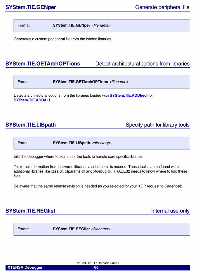
SYStem.TIE.GENper Generate peripheral file
Generates a custom peripheral file from the loaded libraries.
SYStem.TIE.GETArchOPTions Detect architectural options from libraries
Detects architectural options from the libraries loaded with SYStem.TIE.ADDtiedll or SYStem.TIE.ADDALL.
SYStem.TIE.LIBpath Specify path for library tools
tells the debugger where to search for the tools to handle core specific libraries.
To extract information from delivered libraries a set of tools is needed. These tools can be found within additional libraries like xtisa.dll, xtparams.dll and xtdebug.dll. TRACE32 needs to know where to find these files.
Be aware that the same release revision is needed as you selected for your XGP request to Cadence®.
SYStem.TIE.REGlist Internal use only
Format: SYStem.TIE.GENper <filename>
Format: SYStem.TIE.GETArchOPTions <filename>
Format: SYStem.TIE.LIBpath <directory>
Format: SYStem.TIE.REGlist <filename>
XTENSA Debugger 66 ©1989-2018 Lauterbach GmbH

CPU specific TERM.METHOD Command
TERM.METHOD Define communication protocol
For a description of the other options, see TERM.METHOD.
Format: TERM.METHOD BRK1_14 [<address>]
BRK1_14 The command TERM.METHOD BRK1_14 tells the debugger to use GNU SYSCALL operations for terminal communication.Use TERM.view to open the terminal window and to activate the communication.When an application reaches “break 1,14”, the application is stopped and the debugger checks for the type of SYSCALL.• When receiving a SYSCALL_WRITE operation, the debugger writes the
relevant information to the terminal window and returns to Go state, i.e. starts to execute user code again.
• When receiving a SYSCALL_READ, the application remains stopped. The debugger is waiting for some input to the terminal window. When you press the Enter key, the application resumes operation.
The handling of "break 1,14" is only active when the TERM.view window is open while TERM.METHOD BRK1_14 is selected. In all other cases, "break 1,14" is treated as a normal software break instruction.
XTENSA Debugger 67 ©1989-2018 Lauterbach GmbH

CPU specific TrOnchip Commands
The TrOnchip command group provides full access to both ICE Breaker units called A and B. Most of the features can also utilized easier by setting regular breakpoints (Break.Set command).
The TrOnchip commands are only visible if the debugger detects TRAX-PC hardware. They cannot be modified when the onchip trace is disabled.
For the bit descriptions of the control registers, please refer to the Trace Solutions User’s Guide of the chip/core manufacturer.
TrOnchip.RESet Reset on-chip trigger settings
Resets all TrOnchip settings.
TrOnchip.state Display on-chip trigger window
Opens the TrOnchip.state window.
Format: TrOnchip.RESet
Format: TrOnchip.state
XTENSA Debugger 68 ©1989-2018 Lauterbach GmbH

JTAG Connection
Mechanical Description of the 14-pin Debug Cable
Tensilica has specified Pin 8 as a mechanical KEY Pin to define the orientation of the connector. This is a standard 14 pin double row (two rows of seven pins) connector (pin to pin spacing: 0.100 in.).
Electrical Description of the 14-pin Debug Cable
• TCK, TMS, TDI and nTRST are driven by CMOS drivers which are supplied with a voltage following the level at VCCS. Therefore the ICD can work in an voltage range of 1.8 … 5.0 V. In normal operation mode this driver is enabled, but it can be disabled to give another tool access to the JTAG port. In environments where multiple tools can access the JTAG port, it is absolutely required that there is a pull down resistor at TCK. This is to ensure that TCK is low during a hand over between different tools.
• TDO is ICD input only and needs standard TTL level.
• VCCS is used as a sense line for the target voltage. It is also used to define the level which is generated to supply the output drivers of the ICD interface to make an adaptation to the target voltage (I(VCCS) appr. 3 mA).
• nRESET (= nSRST) is used by the debugger to reset the target CPU or to detect a reset on the target. It is driven by an open collector buffer. The debugger will only assert a pulse on nRESET when the SYStem.Up command is executed.
Signal Pin Pin SignalTDI 1 2 GND
TDO 3 4 GNDTCK 5 6 GNDN/C 7 - KEY PIN
RESET- 9 10 TMSVCCS 11 12 N/C
N/C 13 14 TRST-
XTENSA Debugger 69 ©1989-2018 Lauterbach GmbH

Support
Available Tools
CP
U
ICE
FIR
E
ICD
DE
BU
G
ICD
MO
NIT
OR
ICD
TR
AC
E
PO
WE
RIN
TE
GR
ATO
R
INS
TR
UC
TIO
NS
IMU
LA
TOR
CUSTOM_CPU YESCUSTOM_DSP YESDC_108MINI YESDC_212GP YESDC_232L YESDC_330HIFI YESDC_454CK YESDC_570T YESHIFI YESXTENSA_9 YESXTENSA_LX2 YESXTENSA_LX3 YESXTENSA_LX4 YESXTENSA_LX5 YESXTENSA_LX6 YESXTENSA_LX7 YES
XTENSA Debugger 70 ©1989-2018 Lauterbach GmbH

Compilers
Target Operating Systems
Language Compiler Company Option Comment
C++ GNU Free Software Foundation, Inc.
ELF/DWARF
Company Product Comment
freeRTOS FreeRTOS up to v9Express Logic Inc. ThreadX- XOS
XTENSA Debugger 71 ©1989-2018 Lauterbach GmbH

3rd-Party Tool Integrations
CPU Tool Company Host
WINDOWS CE PLATF. BUILDER
- Windows
CODE::BLOCKS - -C++TEST - WindowsADENEO -X-TOOLS / X32 blue river software GmbH WindowsCODEWRIGHT Borland Software
CorporationWindows
CODE CONFIDENCE TOOLS
Code Confidence Ltd Windows
CODE CONFIDENCE TOOLS
Code Confidence Ltd Linux
EASYCODE EASYCODE GmbH WindowsECLIPSE Eclipse Foundation, Inc WindowsCHRONVIEW Inchron GmbH WindowsLDRA TOOL SUITE LDRA Technology, Inc. WindowsUML DEBUGGER LieberLieber Software
GmbHWindows
SIMULINK The MathWorks Inc. WindowsATTOL TOOLS MicroMax Inc. WindowsVISUAL BASIC INTERFACE
Microsoft Corporation Windows
LABVIEW NATIONAL INSTRUMENTS Corporation
Windows
RAPITIME Rapita Systems Ltd. WindowsRHAPSODY IN MICROC IBM Corp. WindowsRHAPSODY IN C++ IBM Corp. WindowsDA-C RistanCASE WindowsTRACEANALYZER Symtavision GmbH WindowsECU-TEST TraceTronic GmbH WindowsUNDODB Undo Software LinuxTA INSPECTOR Vector WindowsVECTORCAST UNIT TESTING
Vector Software Windows
VECTORCAST CODE COVERAGE
Vector Software Windows
XTENSA Debugger 72 ©1989-2018 Lauterbach GmbH

Products
Product Information
OrderNo Code Text
LA-3760 JTAG-XTENSA
JTAG Debugger for Xtensa 14 Pinsupports Xtensa Cores from Tensilicaincludes software for Windows, Linux and MacOSXrequires Power Debug Moduledebug cable with 14 pin connector
LA-3760A JTAG-XTENSA-A
JTAG Debugger License for Xtensa Add.supports Xtensa Cores from Tensilicaplease add the base serial number of your debugcable to your order
LA-3762 JTAG-XTENSA-20
JTAG Debugger for Xtensa 20 Pinsupports Xtensa Cores from Tensilicavia an ARM JTAG interfaceincludes software for Windows, Linux and MacOSXrequires Power Debug Moduledebug cable with 20 pin connector
LA-3761 JTAG-AD-XTENSA
JTAG Converter XTENSA/XTAV60 TargetXTENSA JTAG Adapter toXTAV60 Target14 pin to 50 pinBoards: XTAV60
LA-3763 CON-ARM20-XTENSA14
Converter ARM20 to XTENSA14allows to connect LA-3762 to boards designed for LA-3760
XTENSA Debugger 73 ©1989-2018 Lauterbach GmbH

Order Information
Order No. Code Text
LA-3760 JTAG-XTENSA JTAG Debugger for Xtensa 14 PinLA-3760A JTAG-XTENSA-A JTAG Debugger License for Xtensa Add.LA-3762 JTAG-XTENSA-20 JTAG Debugger for Xtensa 20 PinLA-3761 JTAG-AD-XTENSA JTAG Converter XTENSA/XTAV60 TargetLA-3763 CON-ARM20-XTENSA14 Converter ARM20 to XTENSA14
Additional OptionsLA-4585 COB-DCI-OOB Package CombiProbe Intel® DCI OOBLA-4580 COB-MIPI60-CV2 Package CombiProbe MIPI60-Cv2LA-4581 COB-MIPI60-CV2-L Package CombiProbe MIPI60-Cv2 LongLA-7843A JTAG-ARMV7-A/R-A JTAG Debugger Lic. Cortex-A/-R (32-bit) Add.LA-3743A JTAG-ARMV8-A-A JTAG Debugger Lic. Cortex-A/R (ARMv8) Add.LA-7844A JTAG-CORTEX_M-A JTAG Debugger License for Cortex-M Add.LA-7960X MULTICORE-LICENSE License for Multicore Debugging
XTENSA Debugger 74 ©1989-2018 Lauterbach GmbH