xmem+ - scidyne corporationuser’s reference manual xmem+ external memory plus parallel bus...
TRANSCRIPT

USER’S REFERENCE MANUAL
XMEM+ External Memory plus
Parallel Bus Expansion Capability for Arduino / Genuino MEGA 2560, MEGA ADK
Model No. 100-7699
Doc. No. M7699 Rev: 1.01 12/28/15
649 School Street / Pembroke, MA 02359 USA / Tel: (781) 293-3059
www.scidyne.com

© Copyright 2015
SCIDYNE Corporation
“All Rights Reserved”
Previous revision: 1.00 7/23/15
DISCLAIMER: This document contains proprietary
information regarding SCIDYNE and
its products. The information is
subject to change without notice.
SCIDYNE makes no warranty of any
kind with regard to this material,
including but not limited to, the
implied warranties of merchantability
and fitness for a particular purpose.
SCIDYNE shall not be liable for
errors contained herein or for
incidental or consequential damages
in connection with the furnishing,
performance, or use of this material.
No part of this document may be
duplicated in any form without prior
written consent of SCIDYNE.
WARRANTY:
SCIDYNE warrants this product
against defects in materials and
workmanship and, that it shall conform to specifications current at
the time of shipment, for a period of
one year from date of shipment.
Duration and conditions of warranty
may be superseded when the product
is integrated into other SCIDYNE
products. During the warranty period,
SCIDYNE will, at its option and
without charge to Buyer, either repair
or replace products which prove
defective. Repair or replacement of a
defective product or part thereof does
not extend the original warranty
period.
WARRANTY SERVICE:
For warranty service or repair, this
product must be returned to a service
facility designated by SCIDYNE.
The Buyer must obtain prior approval
and a Return Material Authorization
(RMA) number before returning any products. The RMA number must be
clearly visible on the shipping
container. The Buyer shall prepay
shipping and insurance charges to the
service facility and SCIDYNE shall
pay shipping and insurance charges to
Buyer’s facility for products repaired
or replaced. SCIDYNE may, at its
discretion, bill the Buyer for return
shipping and insurance charges for
products received for repair but
determined to be non-defective.
Additionally, the Buyer shall pay all
shipping charges, duties and taxes for products returned to SCIDYNE from
another country.
LIMITATION OF WARRANTY:
The forgoing warranty shall not apply
to defects resulting from improper or
negligent maintenance by the Buyer,
Buyer-supplied products or
interfacing, unauthorized
modifications or misuse, operation
outside the published specifications of
the product or improper installation
site preparation or maintenance, or the
result of an accident. The design and
implementation of any circuit using
this product is the sole responsibility
of the Buyer. SCIDYNE does not
warrant the Buyer’s circuitry or
malfunctions of SCIDYNE products
that result from the Buyer’s circuitry.
In addition, SCIDYNE does not
warrant any damage that occurs as a result of the Buyer’s circuit or any
defects that result from Buyer-
supplied products. This Warranty
does not cover normal preventative
maintenance items such as fuse
replacement, lamp replacement,
resetting of circuit breakers, cleaning
of the Product or problems caused by
lack of preventative maintenance,
improper cleaning, improper
programming or improper operating
procedures. No other warranty is
expressed or implied. SCIDYNE
specifically disclaims the implied
warranties of merchantability and
fitness for a particular purpose. Some
states do not permit limitation or
exclusion of implied warranties;
therefore, the aforesaid limitation(s)
or exclusion(s) may not apply to the
Buyer. This warranty gives you
specific legal rights and you may have
other rights which vary from state to state.
CERTIFICATION:
Testing and other quality control
techniques are utilized to the extent
SCIDYNE deems necessary to
support this warranty. Specific testing
of all parameters is not necessarily performed, except those mandated by
government requirements.
30-DAY PRODUCT
EVALUATION POLICY:
SCIDYNE offers a no-risk trial for
initial, low quantity, evaluation
purchases. Items purchased for
evaluation can be returned within 30
days of purchase for a full refund less
shipping charges. The Buyer must
obtain a Return Material
Authorization (RMA) number before
returning any products. The entire
package, including hardware,
software, documentation, discount
coupons and any other accessories
supplied must be returned intact and
in new and working condition. This
policy will not be honored for
packages that are not returned
complete and intact. The Buyer shall prepay shipping and insurance
charges to SCIDYNE. To expedite
the return process, the RMA number
must be clearly visible on the shipping
container. SCIDYNE will cancel the
invoice, refund by check or issue
credit to your credit card within 10
days after receipt of returned
merchandise.
LIFE SUPPORT POLICY:
Certain applications may involve the
risks of death, personal injury or
severe property or environmental
damage (“Critical Applications”).
SCIDYNE products are not designed,
intended, authorized or warranted to
be suitable for use in life-support
applications, devices or systems or
other critical applications without the
express written approval of the
president of SCIDYNE.
Table of Contents
Conventions and Terminology Used in this Publication................................................................................ 4
Introduction....................................................................................................................................................... 2
Key Features ................................................................................................................................................. 3 512KB External SRAM ........................................................................................................................... 3
Parallel Bus Expansion............................................................................................................................. 3
Buffered SPI Signals ................................................................................................................................ 3
Standard Arduino MEGA R3 Connector Layout ................................................................................... 3 Component Identification............................................................................................................................. 4
External Memory Interface .............................................................................................................................. 5
XMCRA - External Memory Control Register A....................................................................................... 5
XMCRB - External Memory Control Register B ....................................................................................... 5 Re-Assigned Digital I/O Ports ..................................................................................................................... 6
Memory Map................................................................................................................................................. 6
SRAM................................................................................................................................................................ 7
Arduino Memory Segments ( .data, .bss, heap, stack ) ........................................................................... 7 Accessing and using the XMEM+ SRAM.................................................................................................. 8
Use Internal Memory for heap................................................................................................................. 8
Relocate the heap to External Memory................................................................................................... 8
Using Memory Banks............................................................................................................................... 9 BSEL - Bank Select Register............................................................................................................... 9
Bank Switching Management............................................................................................................ 10
Parallel Bus Expansion................................................................................................................................... 12
Data Bus ...................................................................................................................................................... 12 Address Bus ................................................................................................................................................ 12
Control Signals............................................................................................................................................ 12
VBUS ......................................................................................................................................................... 12
RD*.......................................................................................................................................................... 12 WR*......................................................................................................................................................... 12
EN*.......................................................................................................................................................... 12
RESOUT ................................................................................................................................................. 12
Write and Read Operations ........................................................................................................................ 13 Timing Diagram.......................................................................................................................................... 13
Adding Wait-States for Accessing Slower Devices ................................................................................. 14
Defining External Memory Sectors....................................................................................................... 14
Setting Wait-State Timing ..................................................................................................................... 14 Hardware Examples.................................................................................................................................... 15
82C55A Peripheral Interface ................................................................................................................. 15
Address Decoding Circuits .................................................................................................................... 16
SPI Bus Signals........................................................................................................................................... 17 MISO - Master-In-Slave-Out................................................................................................................. 17
MOSI - Master-Out-Slave-In................................................................................................................. 17
SCK - Serial Clock ................................................................................................................................. 17
Specifications .................................................................................................................................................. 18 Appendix-A: Schematic Diagram.................................................................................................................. 19
User Notes ....................................................................................................................................................... 20

㍰
Conventions and Terminology Used in this Publication
Safety and Usage Conventions
Note:
Provides important information and useful tips that will assist in
the understanding and operation of this product.
Caution:
Calls attention to a procedure, practice, or condition that could
possibly cause equipment damage or bodily injury.
Danger:
Calls attention to a procedure, practice, or condition that is likely
to cause extensive equipment damage, severe bodily injury, or
death if not observed.
Terminology
Logic Conditions
Unless otherwise noted, logic signals are designated as TRUE (Set) and FALSE (Clear). Names with an
asterisk (*) postscript are inverted or active low. Unless otherwise noted TRUE is considered logic '1'
(+5Vdc or +3.3Vdc) and FALSE is considered logic '0' (0Vdc).
Numbering Systems
Computerized equipment often requires its numeric data to be represented in different forms depending
on the audience and information being conveyed. Decimal numbers are typically used for end-user data entry and display while internally these values are converted and manipulated in native binary.
Hexadecimal numbers are often used by programmers as an intermediate level between binary and
decimal notations.
Base Name Format (MS ←−−→ LS)
2 Binary 0b10111001 or 1011 10012
10 Decimal 185
16 Hexadecimal 0xB9 or B916 or HB9
Multi-Byte Word Formats Unless otherwise specified numbers or registers spanning multiple bytes are stored in “little endian” format. The first address (ADDR+0) will contain the Least Significant Byte (LSB) while the Most
Significant Byte (MSB) will reside at the highest address.
ADDR+0 ADDR ADDR+n
LSB LS ←−−→ MS MSB

Page 2
Introduction The XMEM+ is a peripheral board which enhances a standard Arduino MEGA 2560 or
MEGA ADK in two significant ways:
1. Increasing the amount of available SRAM
2. Adding true Parallel Bus Expansion capability
Unless noted separately, in the context of this document
MEGA will be used to mean both the Arduino (Genuino) MEGA 2560 and MEGA ADK microcontroller board products.
The Arduino MEGA features the ability to add memory and I/O space outside of it's
internal 8KB SRAM. The mechanism is built-in to the Atmel ATMEGA2560-16AU microcontroller and requires only minimal supporting hardware and software to apply.
Except for the nineteen I/O lines needed to implement the external memory interface, no
other Arduino signals are necessary. The external space appears seamlessly within the
Arduino memory map and operates at full bus speed (no Wait-States). The XMEM+ is designed specifically to take full advantage of the External Memory interface feature.
The product name XMEM refers to eXternal MEMory as
described in the Atmel data sheet for the ATMEGA2560 microcontroller. The plus (+) refers to the inclusion of the
expansion bus.
Figure 1 - XMEM+ Simplified Block Diagram
A B
DIR
BUFFER
BA
BUFFERED
CONTROL BUS
and SPI BUS
V CC
V CC
BUFFEREDDATA BUS
BUFFER
BUFFERED
ADDRESS BUS
BUFFER
B
V CC
A
HIGH-SPEED
LOGICA D[7 :0]
A DDRE SS[15:8]
A [7:0]
BSEL[3:0]
EN_BUS*
BUS_ DIR
EN_RAM*
DATA[7:0]
ADDRE SS[15:0]
M7699-01
A TMEGA25 60-16AUMicro co n troller
P ORTA [7:0]
P ORTC[7:0]
PORTG.0
RESET
+5V
+3.3V
A D[7 :0]
A DDRE SS[15:8]
ALEALE
WR*WR*
CONTROL
RD*RD*
RESETRESET
+5V
+3.3V
GND GND
CONTROL
DATA[7:0]
512KB
SRAM
ADDR[14 :0]
A18
A17
A16
A15
BSEL.3
BSEL.2
BSEL.1
BSEL.0
WR*
RD*
E N_RAM*
WR*
RD*
EN_RAM*
BUS_ DIR
RESETMOSI
MISO
SCK
XMCRA.S RE = "1"
A [7:0]
P ORTG.1
PORTG.2
WR*
RD*
ALE
+3.3V +5V
V
B US LOGICVOLTAGE
MEGA2560
MEGA ADK
XMEM+
SCK
MOSI
MISO
S PI BUS
EXPANSION
BUS
V
MISO

ⴠل
Page 3
Key Features 512KB External SRAM A standard MEGA provides only 8,192 bytes (8KB) of SRAM which must be divided
amongst the stack, heap, and data purposes. As an Arduino program grows in complexity
available SRAM can be quickly used up. Adding the XMEM+ to an Arduino MEGA
system increases SRAM space by up to 512KB. The additional SRAM is organized as 16 banks of 32KB each. The active bank is directly accessible within the MEGA memory
space between address 0x2200 and 0xA1FF. All address and bank decoding is controlled
by software using on-board High-Speed logic. The additional SRAM makes the MEGA
much better suited and easier to use in applications requiring large amounts of fast memory such as buffering data before writing to an SD Card, servicing network
communications, or generating graphic display information.
Parallel Bus Expansion The XMEM+ provides the user with a fixed 23K byte area for connecting custom parallel type circuitry. Buffered Read, Write, Enable, Reset, 8-bit Data, and 16-bit Address
signals are fully accessible for off-board prototyping. This area is true Arduino memory,
supporting all software instructions and running at full bus speed. The logic voltage of
the buffers can be set to operate at either 3.3V or 5V in order to perform proper translation when working with modern mixed voltage circuitry.
Buffered SPI Signals As an additional benefit, the MOSI and SCK Serial-Peripheral-Interface (SPI a.k.a. ICSP)
signals are also routed through buffers. The ability to provide voltage translation from
5V down to 3.3V is particularly handy when connecting to modern 3.3V only type SPI devices.
Standard Arduino MEGA R3 Connector Layout The XMEM+ is the same overall size of a standard Arduino MEGA 2560 microcontroller
board. The connector pattern follows the R3 format and has been designed to plug directly on top by means of stack-through connectors.

Page 4
Component Identification Before putting the XMEM+ in to service is helpful to become familiar with it's various
components.
M7699-02
1 1 1
4 3 1 1 11
1
2
Figure 2 - Component Identification
(1) Standard Arduino MEGA connections
The XMEM+ features stack-though connectors which allows additional peripheral boards
to be mounted on top of one another in a piggy-back arrangement.
(2) Parallel Bus Expansion
These connectors form the Parallel Bus Expansion (a.k.a. Expansion Bus) consisting of
an 8-bit bi-directional Data bus, 16-bit Address bus, and Control signals. When prototyping external circuits, wires can be inserted in to these connectors to gain access
to the individual signals. Most signals are buffered and the logic operating voltage is
determined by the position of the Bus Logic Voltage Selection Jumper JP1 (3).
(3) Bus Logic Voltage selection, JP1
The Expansion Bus logic can be operated at either 3.3V or 5V depending on the
requirements of the user's circuitry.
The operating voltage for the Bus Logic must be carefully chosen to match the intended external circuitry. Attempting to drive external 3.3V
circuits with 5V can damage the circuitry and stress the XMEM+. The buffers used on the XMEM+ when operated at 3.3V safely tolerate 5V
signal levels coming from external circuitry.
(4) Reset Push Button Momentarily pressing this button will reset the entire Arduino system.
Page 5
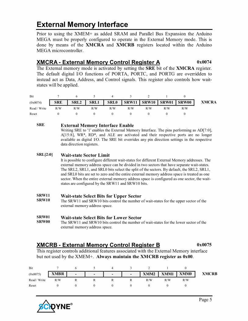
External Memory Interface Prior to using the XMEM+ as added SRAM and Parallel Bus Expansion the Arduino
MEGA must be properly configured to operate in the External Memory mode. This is done by means of the XMCRA and XMCRB registers located within the Arduino
MEGA microcontroller.
XMCRA - External Memory Control Register A 0x0074
The External memory mode is activated by setting the SRE bit of the XMCRA register.
The default digital I/O functions of PORTA, PORTC, and PORTG are overridden to
instead act as Data, Address, and Control signals. This register also controls how wait-states will be applied.
Bit 7 6 5 4 3 2 1 0
(0x0074) SRE SRL2 SRL1 SRL0 SRW11 SRW10 SRW01 SRW00 XMCRA
Read / Write R/W R/W R/W R/W R/W R/W R/W R/W
Reset 0 0 0 0 0 0 0 0
SRE External Memory Interface Enable
Writing SRE to '1' enables the External Memory Interface. The pins performing as AD[7:0],
A[15:8], WR*, RD*, and ALE are activated and their respective ports are no longer
available as digital I/O. The SRE bit overrides any pin direction settings in the respective
data direction registers.
SRL[2:0] Wait-state Sector Limit
It is possible to configure different wait-states for different External Memory addresses. The
external memory address space can be divided in two sectors that have separate wait-states.
The SRL2, SRL1, and SRL0 bits select the split of the sectors. By default, the SRL2, SRL1,
and SRL0 bits are set to zero and the entire external memory address space is treated as one
sector. When the entire external memory address space is configured as one sector, the wait-
states are configured by the SRW11 and SRW10 bits.
SRW11
SRW10 Wait-state Select Bits for Upper Sector The SRW11 and SRW10 bits control the number of wait-states for the upper sector of the
external memory address space.
SRW01
SRW00 Wait-state Select Bits for Lower Sector The SRW11 and SRW10 bits control the number of wait-states for the lower sector of the
external memory address space.
XMCRB - External Memory Control Register B 0x0075
This register controls additional features associated with the External Memory interface
but not used by the XMEM+. Always maintain the XMCRB register as 0x00.
Bit 7 6 5 4 3 2 1 0
(0x0075) XMBRK
- - - - XMM2 XMM1 XMM00
XMCRB
Read / Write R/W R R R R R/W R/W R/W
Reset 0 0 0 0 0 0 0 0
낐
Page 6
ExpansionBus
XMEM+REGISTERS
SRAM32K Bytes
BANK-0
( Default )
SRAM8,192 Bytes
0xFFFF
0xA2000xA1FF
0x21FF
0x2200
0x0000
151 2
M7699-03
0xFF00
0xFEFF
ExternalMemorySpace
InternalMemorySpace
.data
.bss
stack
heap
availableSRAM
MEGA
REGISTERS
0x02000x01FF
Example C code:
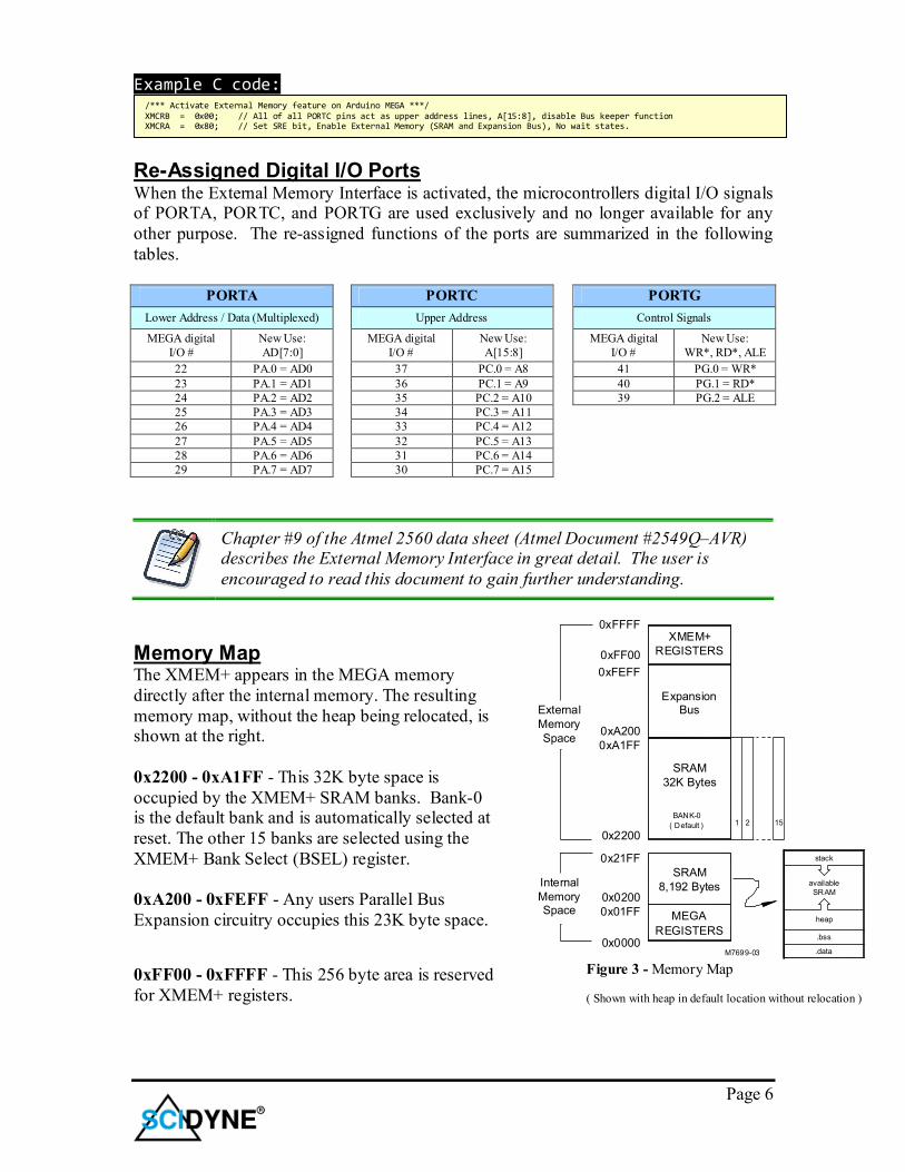
Re-Assigned Digital I/O Ports When the External Memory Interface is activated, the microcontrollers digital I/O signals of PORTA, PORTC, and PORTG are used exclusively and no longer available for any
other purpose. The re-assigned functions of the ports are summarized in the following
tables.
PORTA PORTC PORTG
Lower Address / Data (Multiplexed) Upper Address Control Signals
MEGA digital
I/O #
New Use:
AD[7:0]
MEGA digital
I/O #
New Use:
A[15:8]
MEGA digital
I/O #
New Use:
WR*, RD*, ALE
22 PA.0 = AD0 37 PC.0 = A8 41 PG.0 = WR*
23 PA.1 = AD1 36 PC.1 = A9 40 PG.1 = RD*
24 PA.2 = AD2 35 PC.2 = A10 39 PG.2 = ALE
25 PA.3 = AD3 34 PC.3 = A11
26 PA.4 = AD4 33 PC.4 = A12
27 PA.5 = AD5 32 PC.5 = A13
28 PA.6 = AD6 31 PC.6 = A14
29 PA.7 = AD7
30 PC.7 = A15
Chapter #9 of the Atmel 2560 data sheet (Atmel Document #2549Q–AVR) describes the External Memory Interface in great detail. The user is
encouraged to read this document to gain further understanding.
Memory Map The XMEM+ appears in the MEGA memory
directly after the internal memory. The resulting
memory map, without the heap being relocated, is shown at the right.
0x2200 - 0xA1FF - This 32K byte space is
occupied by the XMEM+ SRAM banks. Bank-0 is the default bank and is automatically selected at
reset. The other 15 banks are selected using the
XMEM+ Bank Select (BSEL) register.
0xA200 - 0xFEFF - Any users Parallel Bus
Expansion circuitry occupies this 23K byte space.
0xFF00 - 0xFFFF - This 256 byte area is reserved
for XMEM+ registers.
/*** Activate External Memory feature on Arduino MEGA ***/ XMCRB = 0x00; // All of all PORTC pins act as upper address lines, A[15:8], disable Bus keeper function XMCRA = 0x80; // Set SRE bit, Enable External Memory (SRAM and Expansion Bus), No wait states.
Figure 3 - Memory Map ( Shown with heap in default location without relocation )

Page 7
SRAM The XMEM+ provides up to 512K bytes of SRAM to an Arduino MEGA. The SRAM is
organized as 16 banks of 32KB each. Only one bank may be active at a time and will always appear in the same memory range, between addresses 0x2200 - 0xA1FF. The
default bank at power-on or system reset is automatically set to bank-0 by the on-board
High-Speed logic.
Arduino Memory Segments ( .data, .bss, heap, stack ) In general, internal SRAM memory on an Arduino MEGA is divided amongst four
different segments each used for specific purpose as summarized here.
.data Stores initialized static variables
The data segment variables are given a known value before the program begins running. The initial values for the data segment reside in non-volatile memory (i.e.; FLASH or EEPROM) and gets copied to the
corresponding SRAM memory locations after reset but before program execution. This is considered compile-time allocation as the software programmer has previously and consciously determined the type of,
how many, and the initial values of the variables.
int foo = 0x1234; // Reserve an integer SRAM variable named foo. At reset it gets loaded with 0x1234
.bss Stores uninitialized static variables
Not all SRAM variables need to have values before a program begins running. For example, a display buffer might only requires some number of byte locations to be set aside and the buffer given a symbolic
name. It isn't important that the locations start with known values because the buffer will be populated with relevant data once the program executes and live display information is generated. Also, data occupying the
.bss segment does not use up non-volatile memory space to hold initialization values. This segment is also
considered compile-time allocation as the software programmer determines the type of and how many variables will be needed.
unsigned char dispbuf[16]; // Reserve 17 bytes of SRAM for a LCD, not Initialized
heap Used for the dynamic allocation of memory
The heap is a segment of SRAM that can be used to allocate large areas of SRAM memory for things like communication buffers or complex data structures. The allocation and management is done by the program
as it executes. It is suggested the heap be relocated to the XMEM+ SRAM.
char * rx_buf = malloc(400); // Allocate 400 bytes in heap for buffer, returns starting address of buffer
stack Used dynamically as temporary storage by processor
The stack segment stores temporary variables such as those created within functions and may also be used to retain critical program states before servicing an interrupt. The stack pointer starts at top of internal RAM
and moves downward as it is used. The stack is automatically managed by the microcontroller's CPU and behaves like a First-in/Last-out data structure. For example, whenever a function declares a new variable, it
is created ("pushed") on the stack and the stack pointer moves lower in SRAM. When the function exits, all of the variables that were temporarily created on the stack are deleted (i.e.; "popped") as the stack pointer
moves back up. Those previously used memory locations are available for future stack variables. Because
the stack is used so frequently and the internal SRAM run faster than external SRAM it is best to use internal SRAM for the stack.

딐Ђ
Page 8
Accessing and using the XMEM+ SRAM Once the External Memory Interface is activated the XMEM+ SRAM can be accessed
and used in several ways:
� Keep all memory segments, including the heap, at their default locations inside the microcontroller.
Accessing the XMEM+ SRAM is done using pointers maintained by the programmer.
� Relocate the heap segment to XMEM+ SRAM but use only the default bank-0 for an additional 32K
bytes.
� Relocate the heap segment to XMEM+ SRAM and use multiple banks by means of bank-switching.
� Combine above methods to satisfy specific application needs.
Use Internal Memory for heap The most basic method to access XMEM+ SRAM is by using pointers managed by the
software programmer. The memory locations are considered private and exist outside the
domain of the C compiler. In this case, the .data, .bss, heap, and stack segments remain
at their default locations inside the internal SRAM of the MEGA microcontroller. Any calls to dynamic memory routines will return pointers to locations within the internal
heap space. Multiple banks can be accessed using the Bank Select Register BSEL.
Example C code:
Relocate the heap to External Memory The preferred use of the XMEM+ SRAM is to relocate the heap. This is done by making
changes to specific linker parameters or by software instructions during the Arduino
setup() function. Beside increasing heap space, relocation also has potential benefit of allowing a deeper stack as it can now use the memory previously occupied by the heap.
To facilitate relocating the heap by software two system variables exist which delineate
its starting and ending addresses. On a stock Arduino MEGA these variables are automatically initialized to locations within the internal SRAM using addresses provided
by the linker. However, the variables can be modified during runtime to instead use
SRAM memory located on the XMEM+.
__malloc_heap_start This 16-bit system SRAM variable defines the starting address of the
heap segment. During initialization, just after reset, this variable is
loaded with the linker generated value __heap_start.
__malloc_heap_end This 16-bit system SRAM variable defines the ending address of the heap
segment. During initialization, just after reset, this variable is loaded with
the linker generated value __heap_end.
Initial changes to these system variables should be done as early as practical in the
programs execution, and definitely before making any function calls that would affect
the heap such as malloc(), calloc(), or free(). Also, Some library functions, notably
those from the stdio.h, may use dynamic memory and should be avoided until the heap
and banks have been properly setup. Subsequent changes during run-time must be
carefully managed especially when performing bank switching.
/*** Create a pointer and load the memory location ***/ char * my_pointer = (char *) = 0x2200; // Point at a location in the XMEM+ memory space *my_pointer = 'A'; // Store the letter A (address 0x2200 contains 0x41, ASCII 'A')

혠ـ
Page 9
Example C code:
If only the 32KB of bank-0 (default) will be used as heap space (no bank switching) then
just __malloc_heap_start and __malloc_heap_end need to be changed. It is not necessary
to manage the two other heap related system variables, namely __brkval and __flp. See
the accompanying example software for details.
Using Memory Banks Some application may require more SRAM than can be satisfied with just the 32KB
provided by the default bank-0. Bank Switching is a technique that allows the currently active memory space between 0x2200 and 0xA1FF to be swapped for other 32KB SRAM
memory spaces, i.e.; bank. The Bank-Select Register within the XMEM+ High-Speed
logic helps simplify the process.
BSEL - Bank Select Register 0xFF01
The Bank Select Register controls which one of the 16 possible 32KB RAM banks appears actively in the Arduino MEGA memory map. Only one bank may be selected at
a time but all are accessed individually within the same address space (0x2200 - 0xA1FF)
when active. The default bank at power-on or system reset is bank-0.
Bit 7 6 5 4 3 2 1 0
(0xFF01) 0 0 0 0 BSEL3 BSEL2 BSEL1 BSEL0 BSEL[3:0
] Read / Write R R R R R/W R/W R/W R/W
Reset 0 0 0 0 0 0 0 0
BSEL[3:0] These four bits are used to select which of the 16 possible 32KB RAM banks currently
appears in the Arduino MEGA memory map between address 0x2200 - 0xA1FF.
Interpreted collectively the BSEL bits form a binary number corresponding to the selected
bank; where for example: 0000 = Bank-0; 1001 = Bank-9. These bit are reset at power-on
or system reset.
Bit[7:4] These bits are not used but should always be written as 0 for future compatibility.
// Initialize the heap to reside in XMEM+ memory __malloc_heap_start = (char *) 0x2200; // Relocate start of heap to start of XMEM+ SRAM __malloc_heap_end = (char *) 0xA1FF; // Relocate end of heap to end of XMEM+ SRAM

딐Ђ
Page 10
Bank Switching Management When using bank switching it is imperative to maintain the exact system heap variables associated with each bank. A structure such as the one show here is useful for saving the
four critical heap variables. By repeating the structure in an array and employing two
simple software routines, the heap variables for all the banks can be saved and restored in
an organized and efficient manner, effectively creating up to 16 separate heaps.
Example C code:
An example program is available for the XMEM+ which suggests a method for handling
bank switching. The two key software functions it provides are described below. Further information can be gleaned by studying the actual code.
void begin( bool heapInXmem_ ) This function MUST BE CALLED ONCE to activate the External Memory space and
initialize the heap storage structures. If heapInXmem is non-zero then the system parameters that control where the heap resides are changed to use the XMEM+ SRAM.
Example C code:
// Structure to hold critical heap variables struct heapState { char *__malloc_heap_start; // Stores starting address of heap space char *__malloc_heap_end; // Stores ending address of heap space void *__brkval; // Stores highest address used in heap void *__flp; // Stores "Free-List" Data Structure pointer } bankHeapStates[ 16 ]; // Create an array of this structure, one structure for each bank
// Restore a bank heap variables void restoreHeap( uint8_t bank_ ) { __malloc_heap_start = bankHeapStates[ bank_ ].__malloc_heap_start; __malloc_heap_end = bankHeapStates[ bank_ ].__malloc_heap_end; __brkval = bankHeapStates[ bank_ ].__brkval; __flp = bankHeapStates[ bank_ ].__flp; }
// Save a bank heap variables void saveHeap( uint8_t bank_ ) { bankHeapStates[ bank_ ].__malloc_heap_start = __malloc_heap_start; bankHeapStates[ bank_ ].__malloc_heap_end = __malloc_heap_end; bankHeapStates[ bank_ ].__brkval = __brkval; bankHeapStates[ bank_ ].__flp = __flp; }
/******************************************************************************************* * Initial setup. You must call this once * heapInXmem_ * If = 1 (true) then the Arduino heap starting and ending addresses are set to use the XMEM+ SRAM. * If = 0 (false) the only the external memory interface is activated. The heap address ARE NOT * reassigned to XMEM+ SRAM. *******************************************************************************************/ void begin( bool heapInXmem_ ) { uint8_t bank; // Temp value used to identify current bank // set up the xmem registers // Activate external memory XMCRB = 0x00; // All of all PORTC pins act as upper address lines, A[15:8], disable Bus keeper function XMCRA = 0x80; // Set SRE bit, Enable xmem+, No wait states. If Wait-states are needed change this value accordingly // initialize the heap states if( heapInXmem_ ) { __malloc_heap_end = static_cast <char *> (XMEM_END); __malloc_heap_start = static_cast <char *> (XMEM_START); } for(bank = 0; bank < MAX_BANKS_USED; bank++) saveHeap( bank ); // set the current bank to zero setMemoryBank(0, false); }
딐Ђ
Page 11
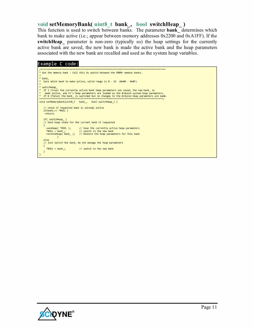
void setMemoryBank( uint8_t bank_, bool switchHeap_ ) This function is used to switch between banks. The parameter bank_ determines which
bank to make active (i.e.; appear between memory addresses 0x2200 and 0xA1FF). If the
switchHeap_ parameter is non-zero (typically so) the heap settings for the currently
active bank are saved, the new bank is made the active bank and the heap parameters associated with the new bank are recalled and used as the system heap variables.
Example C code:
/******************************************************************************************* * Set the memory bank - Call this to switch between the XMEM+ memory banks. * * bank_ * Sets which bank to make active, valid range is 0 - 15 (0x00 - 0x0F) * * switchHeap_ * If 1 (true) the currently active bank heap parameters are saved, the new bank_ is * made active, and it's heap parameters are loaded as the Arduino system heap parameters. * If 0 (false) the bank_ is switched but no changes to the Arduino heap parameters are made. ******************************************************************************************/ void setMemoryBank(uint8_t bank_, bool switchHeap_) { // check if requested bank is already active if(bank_== *BSEL ) return; if( switchHeap_ ) // Save heap state for the current bank if requested { saveHeap( *BSEL ); // Save the currently active heap parameters *BSEL = bank_; // switch in the new bank restoreHeap( bank_ ); // Restore the heap parameters for this bank } else // Just switch the bank, do not manage the heap parameters { *BSEL = bank_; // switch in the new bank } }

딐Ђ
Page 12
Parallel Bus Expansion The Parallel Bus Expansion (a.k.a. Expansion Bus) provides the user with a fixed 23K
byte area for connecting custom parallel type circuitry. Buffered Read, Write, Enable, Reset, 8-bit Data, and 16-bit Address signals are fully accessible for off-board
prototyping. This area is true Arduino MEGA memory space directly supporting all
software instructions and running at full bus speed. Optional Wait-States can be inserted
to accommodate slower parallel devices. The operating logic level for all buffered signals is configurable as 3.3V or 5V in order to perform proper translation when working with
modern mixed voltage circuitry. The External Memory Interface must be running for the
Parallel Bus Expansion to operate.
Data Bus
D[7:0] - These eight signals form the Bi-Directional Data Bus for connecting to external
hardware. D0 is the least significant data bit. The data bus must be used in conjunction with the RD* (read), WR* (write), and EN* (enable) signals.
Address Bus
A[15:0] - These 16 signals form the Address Bus for connecting to external hardware. A0
is the least significant address bit.
Control Signals
VBUS - This is the Bus logic supply voltage. The voltage level can be selected as 3.3V or
5.0V depending on the position of jumper JP1. The user's external circuitry can be
powered from this connection but current draw must not exceed 50ma. Both the 5.0V and
3.3V are supplied directly from the Arduino MEGA2560. If higher currents are required the user's circuitry should employ its own regulated power supply operating at the same
voltage as the Bus Logic JP1 setting.
RD* - READ Active Low. Any software Read operation executed within the address
range of 0xA200 - 0xFEFF will pass a single byte from the external circuitry to the
Arduino MEGA. To be valid the RD* signal must be qualified with the EN* signal.
WR* - WRITE Active Low. Any software Write operation executed within the address
range of 0xA200 - 0xFEFF will pass a single byte from the Arduino MEGA to the
external circuitry. To be valid the WR* signal must be qualified with the EN* signal.
EN* - ENABLE Active Low. Any software operation (Write or Read) within the
address range of 0xA200 to 0xFEFF will activate this signal.
RESOUT - This an output only buffered version of the system reset signal. The signal
is active low during reset and normally idles high at the voltage level determined by the
Bus Logic Voltage jumper setting, JP1.
RESOUT is an Output Only signal designed to drive the reset inputs of external
devices. Manually pulling this signal to ground by means of a switch or other circuitry can damage the RESOUT buffer. External system reset should only be
performed by either pressing a reset button or by momentarily pulling the MEGA
RESET signal to ground.
딐Ђ
Page 13
Write and Read Operations Circuitry connected to the Expansion Bus is accessed using pointers. In general, any valid
pointer type and software technique can be used. However, read-modify-write operations require the externally connected hardware to be both readable and writeable.
Example C code:
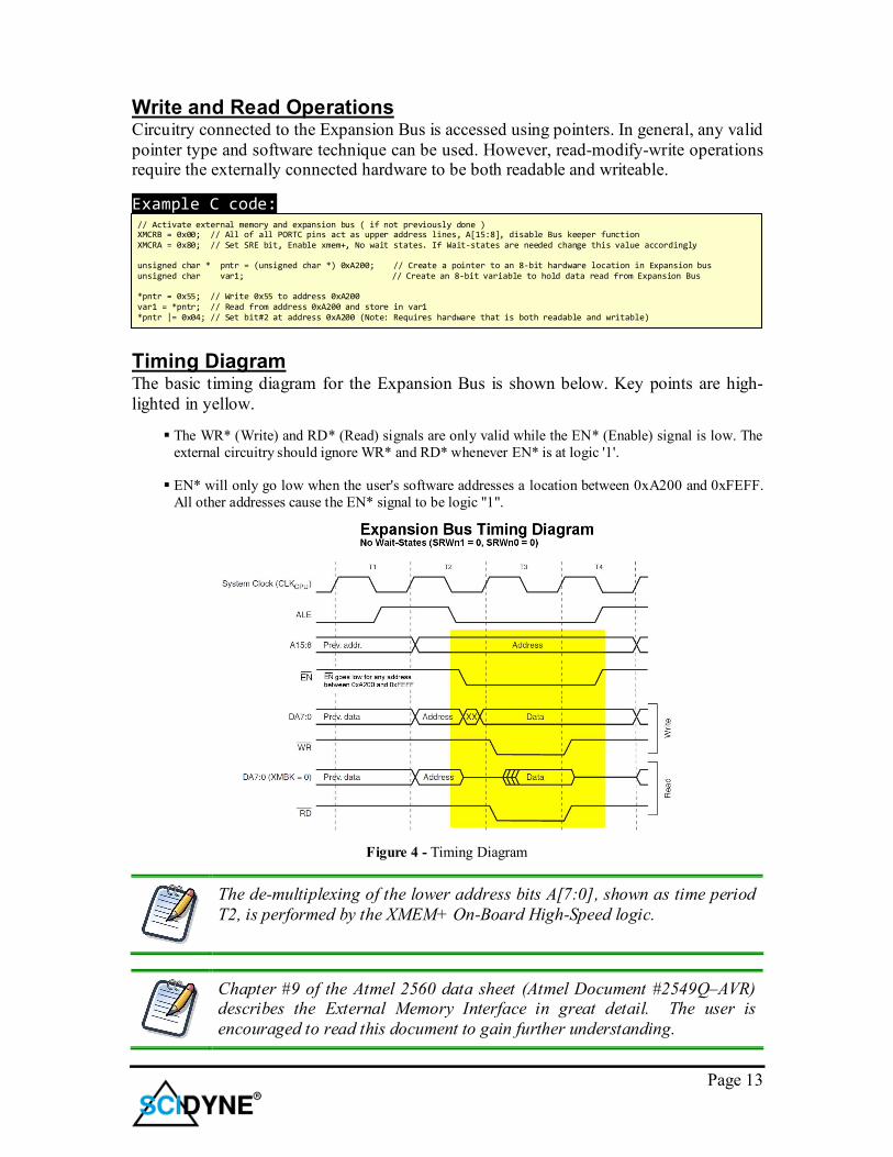
Timing Diagram The basic timing diagram for the Expansion Bus is shown below. Key points are high-
lighted in yellow.
� The WR* (Write) and RD* (Read) signals are only valid while the EN* (Enable) signal is low. The
external circuitry should ignore WR* and RD* whenever EN* is at logic '1'.
� EN* will only go low when the user's software addresses a location between 0xA200 and 0xFEFF.
All other addresses cause the EN* signal to be logic "1".
Figure 4 - Timing Diagram
The de-multiplexing of the lower address bits A[7:0], shown as time period
T2, is performed by the XMEM+ On-Board High-Speed logic.
Chapter #9 of the Atmel 2560 data sheet (Atmel Document #2549Q–AVR) describes the External Memory Interface in great detail. The user is
encouraged to read this document to gain further understanding.
// Activate external memory and expansion bus ( if not previously done ) XMCRB = 0x00; // All of all PORTC pins act as upper address lines, A[15:8], disable Bus keeper function XMCRA = 0x80; // Set SRE bit, Enable xmem+, No wait states. If Wait-states are needed change this value accordingly unsigned char * pntr = (unsigned char *) 0xA200; // Create a pointer to an 8-bit hardware location in Expansion bus unsigned char var1; // Create an 8-bit variable to hold data read from Expansion Bus *pntr = 0x55; // Write 0x55 to address 0xA200 var1 = *pntr; // Read from address 0xA200 and store in var1 *pntr |= 0x04; // Set bit#2 at address 0xA200 (Note: Requires hardware that is both readable and writable)
Page 14
Adding Wait-States for Accessing Slower Devices The XMEM+ uses High-Speed logic and components and is designed to operate at the
full speed of the MEGA without the need for wait-states. However, when connecting to
slower devices it may be desirable or even necessary to add wait-states.
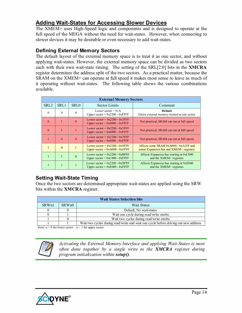
Defining External Memory Sectors The default layout of the external memory space is to treat it as one sector, and without
applying wait-states. However, the external memory space can be divided as two sectors
each with their own wait-state timing. The setting of the SRL[2:0] bits in the XMCRA
register determines the address split of the two sectors. As a practical matter, because the SRAM on the XMEM+ can operate at full speed it makes most sense to leave as much of
it operating without wait-states. The following table shows the various combinations
available.
External Memory Sectors
SRL2 SRL1 SRL0 Sector Limits Comment
0 0 0 Lower sector = N/A
Upper sector = 0x2200 - 0xFFFF Default
Entire external memory treated as one sector
0 1 0 Lower sector = 0x2200 - 0x3FFF Upper sector = 0x4000 - 0xFFFF
Not practical, SRAM can run at full speed
0 1 1 Lower sector = 0x2200 - 0x5FFF Upper sector = 0x6000 - 0xFFFF
Not practical, SRAM can run at full speed
1 0 0 Lower sector = 0x2200 - 0x7FFF Upper sector = 0x8000 - 0xFFFF
Not practical, SRAM can run at full speed
1 0 1 Lower sector = 0x2200 - 0x9FFF Upper sector = 0xA000 - 0xFFFF
Affects some SRAM 0xA000 - 0xA1FF and entire Expansion bus and XMEM+ registers
1 1 0 Lower sector = 0x2200 - 0xBFFF Upper sector = 0xC000 - 0xFFFF
Affects Expansion bus starting at 0xC000 and the XMEM+ registers
1 1 1 Lower sector = 0x2200 - 0xDFFF Upper sector = 0xE000 - 0xFFFF
Affects Expansion bus starting at 0xE000 and the XMEM+ registers
Setting Wait-State Timing Once the two sectors are determined appropriate wait-states are applied using the SRW
bits within the XMCRA register.
Wait States Selection bits
SRWn1 SRWn0 Wait States
0 0 Default, No wait-states
0 1 Wait one cycle during read/write strobe
1 0 Wait two cycles during read/write strobe
1 1 Wait two cycles during read/write and wait one cycle before driving out new address
Note: n = 0 for lower sector, n = 1 for upper sector
Activating the External Memory Interface and applying Wait-States is most
often done together by a single write to the XMCRA register during program initialization within setup().

혠ـ
Page 15
Hardware Examples
82C55A Peripheral Interface This circuit illustrates connecting to a common 82C55A chip.
This device provides 24 digital I/O channels that can be used to
interface to keyboards, display, relays and more. The eight Data bits, Address signals, and Control signals connect directly
to the corresponding signals of the XMEM+ expansion bus.
However, because the RESET input of the 82C55A requires an
opposite polarity of that provided by an Arduino, this example uses Arduino digital #7 signal for that purpose.
In the software below the loop forms a simple binary counter
whose values are written to PORTA. As a result PORTA.0 will toggle more frequently than PORTA.1; PORTA.1 more than
PORTA.2 and so on. PORTA.7 will toggle at the lowest
frequency. Probing with an oscilloscope on any of the PORTA pins allows the toggling bits to be observed.
Example C code:
// This program uses the Expansion bus connected to an 82C55A Peripheral Interface chip. In this example all ports of the // 82C555A are made to act as outputs but all valid configuration modes are supported, see the 82C55A data sheet for details. // Because the Expansion bus is so fast a 1 cycle wait-state is applied to reliably access the chip. // Setup Pointers to access the 82C55 Chip unsigned char * PRTA = (unsigned char *) 0xA200; // 82C55 PORTA Register unsigned char * PRTB = (unsigned char *) 0xA201; // 82C55 PORTB Register unsigned char * PRTC = (unsigned char *) 0xA202; // 82C55 PORTC Register unsigned char * CTRL = (unsigned char *) 0xA203; // 82C55 Control Register // Global variables created in .bss area char buf[80]; // A display buffer for using sprintf //************************************************************************ void setup() { // Activate external memory XMCRB = 0x00; // All of all PORTC pins act as upper address lines, A[15:8], disable Bus keeper function XMCRA = 0xD4; // Set SRE bit. Divide space in to two sectors; Lower sector 0x2200-0x9FFF, Upper sector 0xA000-0xFFFF // Apply 1 wait state on Upper segment because the 82C55A is too slow for XMEM+ Parallel Expansion bus // Setup 82C55 pinMode(7, OUTPUT); // Digital #7 to be used as reset for 82C55A digitalWrite(7, HIGH); // Reset 82C55A delay(25); // wait ... digitalWrite(7, LOW); // Remove 82C55A reset *CTRL = 0x8A; // Configure all 82C55A ports as Outputs Serial.begin(9600); // Start serial communications for Arduino IDE debugging monitor sprintf(buf,"Testing Expansion Bus"); Serial.println(buf); } //************************************************************************ void loop() { unsigned char i, b; for ( i = 0; i < 255; i++ ) // Make a binary counter { *PRTA = i; // Write value to PORTA b = *PRTA; // Read back the PORT // Compare and display error if mis-match is found if ( i != b ) { sprintf(buf,"Fail: %02X != %02X", i, b); // Display the mis-match error Serial.println(buf); } } }
82C55A
A0
A1
WR*
RD*
CS*
Peripheral Interface
VCC (+5V)
GND
RESET
XMEM+
Parallel Expansion Bus
To / From
External Circuitry
M7699-04
D0
D1
D2
D3
D4
D5
D6
D7
34
33
32
31
30
29
28
27
36
5
6
35
9
8
26
7
PORTA.0
PORTA.1
PORTA.2
PORTA.3
PORTA.4
PORTA.5
PORTA.6
PORTA.7
4
3
2
1
40
39
38
37
PORTB.0
PORTB.1
PORTB.2
PORTB.3
PORTB.4
PORTB.5
PORTB.6
PORTB.7
18
19
20
21
22
23
24
25
PORTC.0
PORTC.1
PORTC.2
PORTC.3
PORTC.4
PORTC.5
PORTC.6
PORTC.7
14
15
16
17
13
12
11
10
40 Pin DIP
A0
A1
WR*
RD*
EN*
DIG#7
GND
V BUS
D0
D1
D2
D3
D4
D5
D6
D7
JP1 = 5V
Figure 5 - 82C55A Circuit

혠ـ
Page 16
Address Decoding Circuits The expansion bus can address up to 23,808 (0x5D00) individual byte locations. For
simple experimentation, like in the previous example, the entire expansion bus space can be assigned to a single chip by means of the EN* signal. However, this is very wasteful
and not practical as circuitry complexity increases. When a design requires several chips
to be enabled individually the expansion bus space must be sub-decoded. The following
examples shows a few common ways this can be accomplished.
This circuit uses a 74AHC138 chip to created eight
separate enable signals. Each output is active for 64 bytes
within the address ranges shown.
For example, if pointer PNTR was initialized to 0xA380
the instruction *PNTR = 0xA5; would cause output Y6 to
go low during the time the value 0xA5 appears on the data
bus and is written to address 0xA380.
This circuit shows two 74AHC138 chips. Both chips
decode the same expansion bus address locations.
However, because the WR* and RD* signals are used as
additional qualifiers one chip decodes only write operations
and the other decodes only read operations. This circuit is
most useful when connecting to uni-directional bus devices such a latches in the case of writes or tri-state buffers in the
case of reads.
74AHC138
A
B
A6
A7
3-Line to 8-Line Decoder
VCC (+5V)
GNDGND
VBUS
XMEM+Parallel Expansion Bus
Enables ToExternal Circuitry
M7699-05
1
2
16
8
Y0
Y1
Y2
Y3
Y4
Y5
Y6
Y7
15
14
13
12
11
10
9
7
16 Pin DIP
JP1 = 5V
0xA200 - 0xA23F
CA83
0xA240 - 0xA27F
0xA280 - 0xA2BF
0xA2C0 - 0xA2FF
0xA300 - 0xA33F
0xA340 - 0xA37F
0xA380 - 0xA3BF
0xA3C0 - 0xA3FF
G2A*
G2B*
G1
4
5
6
EN*
74AHC138
A
B
A6
A7
3-Line to 8-Line Decoder
VCC (+5V)
GND
XMEM+
Paral lel Expansion BusWrite Strobes
1
2
16
8
Y0
Y1
Y2
Y3
Y4
Y5
Y6
Y7
15
14
13
12
11
10
9
7
16 Pin DIP
0xA200 - 0xA23F
CA83
0xA240 - 0xA27F
0xA280 - 0xA2BF
0xA2C0 - 0xA2FF
0xA300 - 0xA33F
0xA340 - 0xA37F
0xA380 - 0xA3BF
0xA3C0 - 0xA3FF
G2A*
G2B*
G1
4
5
6
EN*
A
B
VCC (+5V)
GNDGND
VBUS
Read Strobes
M7699-06
1
2
16
8
Y0
Y1
Y2
Y3
Y4
Y5
Y6
Y7
15
14
13
12
11
10
9
7
JP1 = 5V
0xA200 - 0xA23F
C3
0xA240 - 0xA27F
0xA280 - 0xA2BF
0xA2C0 - 0xA2FF
0xA300 - 0xA33F
0xA340 - 0xA37F
0xA380 - 0xA3BF
0xA3C0 - 0xA3FF
G2A*
G2B*
G1
4
5
6
WR*
RD*
74AHC1383-Line to 8-Line Decoder
16 Pin DIP
Figure 6 - Address Decoder
Figure 7 - Write / Read Decoder Circuitry

혠ـ
Page 17
SPI Bus Signals The Expansion Bus also provides access the Serial-Peripheral-Interface signals (a.k.a.
ICSP).
MISO - Master-In-Slave-Out This is an un-buffered signal routed directly to the Arduino Mega. The external circuitry drives this signal to send serial data to the Arduino.
MOSI - Master-Out-Slave-In This is a buffered version of the MOSI signal originating from the Arduino and operates
at the voltage determined by the Bus Logic Voltage jumper setting, JP1. Serial data is
transmitted from the Arduino to the external circuitry on this signal.
SCK - Serial Clock This is a buffered version of the SCK signal originating from the Arduino and operates at
the voltage determined by the Bus Logic Voltage jumper setting, JP1. The SCK signal is
used to synchronously pace the data serially sent over the MOSI and MISO SPI bus signals.

Page 18
Specifications Description: Add-on board for Arduino (Genuino) MEGA 2560 and MEGA ADK.
Provides up to 512K SRAM plus True Parallel Bus Expansion capability.
SRAM: 512K bytes total additional SRAM. Organized as 16 Banks of 32K each.
Speed: Supports full Arduino bus speed, typically 16MHz system clock, No Wait-States.
Wait-States are optionally programmable via software.
Expansion Bus: Addressable Space: 23KB (23,808 bytes)
Logic: Buffered, Jumper selectable Logic Level
Signal Function Direction Signal Name
Data: Bi-Directional D[7:0] Address: Output A[15:0]
Control: Output WR*, RD*, EN*, Reset-Out
Bus Logic Voltage: Output VBus, Jumper selectable as 3.3V or 5V
Digital Logic Levels:
Parameter JP1 = 3.3V JP1 = 5.0V
VIL 0.9V Max. 1.5V Max.
VIH 2.3V Min., 5V Tolerant 3.5V Min.
VOUT
0V Min.
3.3V Max.
0V Min.
5V Max.
SPI (ICSP): MOSI - Master Out Slave In, Buffered, Jumper selectable 3.3V or 5V
MISO - Master In Slave Out, Non-Buffered
SCK - Clock, Buffered, Jumper selectable 3.3V or 5V
Arduino Connections: Long-Lead Stack-through connectors accommodates additional shields.
All connections accept 0.025" sq. leads and prototype wires.
Power: 8 Pos. x 1 Row
Analog: 8 Pos x 1 Row (2)
Digital: 8 Pos x 1 Row (2), 10 Pos. x 1 Row, 18 Pos. x 2 Row
ICSP: 3 Pos x 2 Row
Power
Requirement: Arduino Supplied, 3.3V and 5V Dimensions: 2.10"W x 4.0"L x 0.75"H overall. Arduino Mega R3 format
Environmental: Operating temperature: 0°C to 70°C
Non-condensing relative humidity: 5% to 95%
Compliance: RoHS
Product Origin: Designed, Engineered, and Assembled in U.S.A. by SCIDYNE® Corporation
using domestic and foreign components.

删ك
Page 19
Appendix-A: Schematic Diagram

衆 ⴠɔ M
Page 20
User Notes