xing-yuanwang,yi-lunwang,suowang,boli,xiao … · 6 ¸ xing-yuanwangetal....
TRANSCRIPT

© 2016 Xing-Yuan Wang et al., published by De Gruyter Open.This work is licensed under the Creative Commons Attribution-NonCommercial-NoDerivs 3.0 License.
Nanophotonics 2016
Supplementary Information Open Access
Xing-Yuan Wang, Yi-Lun Wang, Suo Wang, Bo Li, Xiao-Wei Zhang, Lun Dai*, and Ren-Min Ma*
Lasing Enhanced Surface Plasmon ResonanceSensing
Supplementary figure 1-11Supplementary Discussion 1-3
Figure 1: Observation of the Purcell effect and the transition from spontaneous emission to stimulated emission in time-resolved spectra.(a) Time-resolved spontaneous emission under weak pumping conditions of a CdSe flake on quartz showing a lifetime of about 4.12 ns. (b)Black curve: Time-resolved spontaneous emission under weak pumping conditions of a CdSe nanosquare on Au/MgF2 showing a lifetime ofabout 280 ps. The spontaneous emission rate is enhanced by ~15-fold compared with CdS on quartz owing to the Purcell effect. Blue curve:Time-resolved stimulated emission which shows a much fast lifetime close to the instrument response function (red curve) compared tospontaneous emission.
Xing-YuanWang, Yi-LunWang, SuoWang: State Key Lab for Mesoscopic Physics and School of Physics, Peking University, Beijing 100871,ChinaThese authors contributed equally to this work.Bo Li, Xiao-Wei Zhang: State Key Lab for Mesoscopic Physics and School of Physics, Peking University, Beijing 100871, China*Corresponding Author: Lun Dai, Ren-Min Ma: State Key Lab for Mesoscopic Physics and School of Physics, Peking University, Beijing100871, Chinaand Collaborative Innovation Center of Quantum Matter, Beijing, China, E-mail: [email protected], [email protected]

2 | Xing-Yuan Wang et al.
Figure 2: High-resolution transmission electron microscope (HRTEM) image and selected area electron diffraction (SAED) pattern of the Ausubstrate. HRTEM image (left panel) and SAED pattern (a-h) shows that the gold film is with polycrystalline face-centered cubic structurewhere the grain size diameter is about 50 nm. The SAED patterns in the same grain share the same features.
Figure 3: Selected area electron diffraction (SAED) pattern of the CdSe nanosquare (a) and Au substrate (b) showing in Fig. 1 (d) and (e),respectively.
Lasing Enhanced Surface Plasmon Resonance Sensing | 3
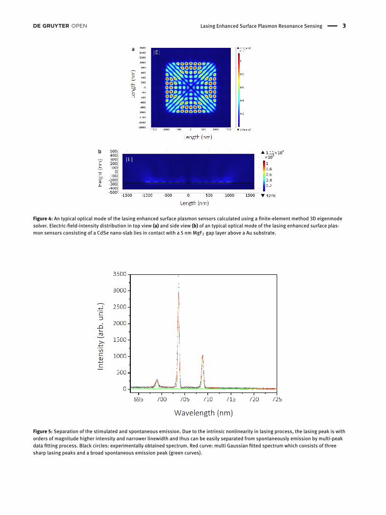
Figure 4: An typical optical mode of the lasing enhanced surface plasmon sensors calculated using a finite-element method 3D eigenmodesolver. Electric-field-intensity distribution in top view (a) and side view (b) of an typical optical mode of the lasing enhanced surface plas-mon sensors consisting of a CdSe nano-slab lies in contact with a 5 nm MgF2 gap layer above a Au substrate.
Figure 5: Separation of the stimulated and spontaneous emission. Due to the intrinsic nonlinearity in lasing process, the lasing peak is withorders of magnitude higher intensity and narrower linewidth and thus can be easily separated from spontaneously emission by multi-peakdata fitting process. Black circles: experimentally obtained spectrum. Red curve: multi Gaussian fitted spectrum which consists of threesharp lasing peaks and a broad spontaneous emission peak (green curves).

4 | Xing-Yuan Wang et al.
Supplementary Discussion 1:plasma dispersion in pumped CdSenanosquaresThe reason for the blue shift in both curves in Fig. 4a isdue to the plasma dispersion effect in CdSe, the gain ma-terial in the device. Since the pump laser changes the den-sity of excited carriers in the CdSe, the real part of the re-fractive index of CdS is then changed due to the plasmadispersion effect [Nano Letters 12 (2012) 5396]. As a result,a linear shift of peak emission wavelength is expected asshown in Fig. 4a. This effect and the wavelength shift canbe modelled as following:
The carrier density in lasing LESPR sensor can be esti-mated through the shift of the peak emission wavelength(λ) which depends on the change of the real part of the re-fractive index (n) by nL= mλ, where L is optical round trippath inside the cavity and m is the mode order. Based onthe Drude-Lorenz equations, we can get the relation of theconcentration of electrons (Ne) and holes (Nh) to the re-fractive index n:
∆n = −e2λ208π2c2ε0n
(∆Nem*ce
+ ∆Nhm*ch
)
where e is electronic charge, λ0 is operating wavelength,c is vacuum light speed, ϵ0 is permittivity of free space,n is refractive index, m*ce (m*ch) is the conductivity effec-tivemass of electrons (holes). Since thephoto-excited elec-trons and holes are dominant carriers in the laser cavity,we assume ∆Ne equals to ∆Nh in a first-order approxima-tion [IEEE Journal of Quantum Electronics QE-23 123-129(1987)]. For CdSe, the refractive index is about 2.8, the ef-fective masses, m*ce (m*ch) are 0.13 (0.45), and the emissionwavelength is 700 nm, we find that ∆n ≈ −7.8 ×10⁻²²∆Ne.Substituting for the observed ∆n in our experiments ofabout 3.2 × 10⁻⁴ (obtained from Fig. 4a), the electron den-sity change, ∆Ne, is about 4.1 × 1017 cm−3. This value in-dicates that the carrier density in the LESPR increases by4.1 × 1017 cm−3 from the transparence carrier density toachieve full laser condition. This value can also reflectthe carrier density necessary to compensate losses in theLESPR cavity.
Supplementary Discussion 2:wavelength sensitivity and figure ofmerit of SPR sensorsThe wavelength sensitivity of a SPR sensors withKretschmann configuration (SFig. 6) can be calculatedas follows:
Sλ =δλrδnef
δnefδn (1)
where(δλrδnef
)prism
= 1dnpdλ
nefnp −
dnefdλ
, where dnefdλ and dnp
dλ de-
scribe the dispersion of the effective index nef of surfaceplasmon and dispersion of the index np of the prism, re-spectively [1].
Figure 6: Diagram of excitation of surface plasmon in theKretschmann geometry. The light wave propagates in the high re-fractive index prism with refractive index np, which is larger thandielectric refractive index nd, and is incident on metal film. A partof the light is reflected, and a part propagates in the metal, whichpenetrates through the thin metal film and couples with the surfaceplasmon at dielectric side.
The δnefδn describes the dependence of the effective in-
dex of the surface plasmon on the refractive index nd ofthe dielectric being sensed, and is decided by the detailsof the dielectric distribution. If we neglect the effect of theprism, the finite-thickness effect of the metal, and the dis-persion of dielectric being sensed (εd = n2d = 1.35882),assume that the permittivity of metal obeys real part ε′m ismuch larger than imaginary part ε′′m, and the dielectric isbulk, Eq. (1) can be simplified as
(Sλ)prism = ε′2m
− n3d2dε′mdλ + ε′m
(n2d + ε
′m) ndnp
dnpdλ
(2)
The wavelength dependence of the Sensitivity (Sλ)prism isshown in SFig. 7.

Lasing Enhanced Surface Plasmon Resonance Sensing | 5
Figure 7: The sensitivity (Sλ)prism as a function of wavelength forSPR sensors. The (Sλ)prism in the near-infrared range is larger thanthe sensitivity in the visible-light range, which is due to the smalldispersion of the prism and SPP.
Forε′m
≫ εd and
ε′m
≫ ε
′′m, the reflectivity can be
approximated to a Lorentzian form with respect to kz, andthen, the full width ∆λ0 at half maximum of the resonancedip for the optimum coupling (In this case, the radiationand absorption losses of the surface plasmon are equal,which makes the depth of the reflectivity dip reaches themaximum) can be calculated as:
∆λ0=4𝛾
dnpdλ
nefnp −
dnefdλ
(3)
Where 𝛾 = Im {β} λ/2π is the attenuation coefficient ofSPP, and β is the propagation constant of the SPP alongthe thin metal film.
If we neglect the effect of the prism and the finite-thickness effect of the metal, and assume that theε′m is much larger than imaginary part ε”m, we have
𝛾 ∼= ε′′m
2(ε′m)2(
εdε′m
εd+ε′m
)3/2, and Eq. (3) can be simplified as [1]:
∆λ0=2ε′′mε3/2d(ε′m
)2 (Sλ)prism (4)
The wavelength dependence of the full width ∆λ0 at halfmaximum of the resonance peak is shown in SFig. 8.
Furthermore, the figure of merit can be calculated as:
FOMλ =(Sλ)prism∆λ0
=
(ε′m)2
2ε′′mε3/2d. (5)
SFig. 9 shows the FOMλ as a function of wavelength forSPR sensors with wavelength modulation.
We note that the permittivity data of Au comes fromJohnson, P. B. & Christy, R. W. Optical Constants of the No-ble Metals [2]. The material of the prism is BK7 glass.
Figure 8: The full width ∆λ0 at half maximum of the resonance peak(FWHM) as a function of wavelength for SPR sensors.
Figure 9: The FOMλ as a function of wavelength for SPR sensorswith wavelength modulation.
Supplementary Discussion 3:Intensity sensitivity and figure ofmerit of SPR sensorsThe intensity sensitivity SI of SPR sensors can be calcu-lated as:
SI=δRδnef
δnefδn , (6)
where R is the reflectivity, nef is the effective index of asurface plasmon, δn the refractive index change of the di-electric being sensed [1]. δR
δnef is the instrumental contri-bution to sensitivity, which has a maximum. The δnef
δn de-scribes the dependence of the effective index of the surfaceplasmon on the refractive index nd of the dielectric being
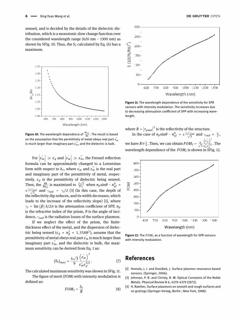
6 | Xing-Yuan Wang et al.
sensed, and is decided by the details of the dielectric dis-tribution, which is amonotonic slow change function overthe considered wavelength range (620 nm – 1300 nm) asshown by SFig. 10. Thus, the SI calculated by Eq. (6) has amaximum.
600 700 800 900 1000 1100 1200 13001.00
1.05
1.10
1.15
1.20
1.25
1.30
1.35
nef/n
Wavelength (nm)
Figure 10: The wavelength dependence of δnefδn . The result is basedon the assumption that the permittivity of metal obeys real part ε′mis much larger than imaginary part ε′′m, and the dielectric is bulk.
Forε′m
≫ εd and
ε′m
≫ ε
′′m, the Fresnel reflection
formula can be approximately changed to a Lorentzianform with respect to kz, where ε
′m and ε′′m is the real part
and imaginary part of the permittivity of metal, respec-tively. εd is the permittivity of dielectric being sensed.Then, the δR
δnef is maximized to 2√3
9𝛾i when npsinθ − n0ef =±𝛾i+𝛾rad√
3 and 𝛾rad = 𝛾i/2 [3] (In this case, the depth ofthe reflectivity dip reduces, and its width decreases, whichleads to the increase of the reflectivity slope) [1], where𝛾i = Im {β} λ/2π is the attenuation coefficient of SPP, npis the refractive index of the prism, θ is the angle of inci-dence, 𝛾rad is the radiation losses of the surface plasmon.
If we neglect the effect of the prism, the finite-thickness effect of the metal, and the dispersion of dielec-tric being sensed (εd = n2d = 1.35882), assume that thepermittivity ofmetal obeys real part ε′m ismuch larger thanimaginary part ε′′m, and the dielectric is bulk, the maxi-mum sensitivity can be derived from Eq. 1 as:
(SI)max =4√3
9
(ε′m)2
ε′′mε3/2d. (7)
The calculatedmaximumsensitivitywas shown inSFig. 11.The figure of merit (FOM) with intensity modulation is
defined as:
FOMI =SIR (8)
Figure 11: The wavelength dependence of the sensitivity for SPRsensors with intensity modulation. The sensitivity increases dueto decreasing attenuation coeflcient of SPP with increasing wave-length.
where R =rpmd
2 is the reflectivity of the structure.In the case of npsinθ − n0ef = ±
𝛾i+𝛾rad√3 and 𝛾rad = 𝛾i
2 ,
we have R∼= 13 . Then, we can obtain FOMI = 4√
3
(ε′m
)2
ε′′m ε3/2d. The
wavelength dependence of the FOMI is shown in SFig. 12.
Figure 12: The FOMI as a function of wavelength for SPR sensorswith intensity modulation.
References[1] Homola, J. I. and Dostálek, J. Surface plasmon resonance based
sensors. (Springer, 2006).[2] Johnson, P. B. and Christy, R. W. Optical Constants of the Noble
Metals. Physical Review B 6, 4370-4379 (1972).[3] H. Raether, Surface plasmons on smooth and rough surfaces and
on gratings (Springer-Verlag, Berlin ; New York, 1988).