xilinx ds253 content-addressable memory v6.1, data sheet · the logicore™ ip content-addressable...
TRANSCRIPT

DS253 September 19, 2008 www.xilinx.com 1
© 2003-2008 Xilinx, Inc. All rights reserved. XILINX, the Xilinx logo, the Brand Window, and other designated brands included herein are trademarks of Xilinx, Inc. All other trademarks are the property of their respective owners.
IntroductionThe LogiCORE™ IP Content-Addressable Memory(CAM) core is a fully verified memory unit that usescontent matching rather than addresses. The coreenables faster data searches as compared to other mem-ory implementations and offers parallel content com-pares to find a valid address. The width, depth,memory type, and other optional features of the CAMcore can be customized using the CORE Generator soft-ware.
Features• CAM depths from 16 to 4096 words
• CAM data widths from 1 to 512
• Selectable memory type: SRL16 or block RAM
• Two ternary modes; SRL16 implementation only
• Encoded (binary), single-match unencoded (one-hot), or multiple-match unencoded match address options
• Two match resolution types: lowest match address or highest match address
• Configurable memory initialization for binary and standard ternary CAMs
ApplicationsCAMs are used in various networking, telecommunica-tions and storage applications because of their parallelfast-search capabilities, for example Ethernet, ATMswitches, IP address resolution, recognition algorithm,databases, and caches.
0
Content-AddressableMemory v6.1
DS253 September 19, 2008 0 0 Product Specification
LogiCORE IP Facts
Core Specifics
Supported Device Family
Virtex®-5, Virtex-4/XA, Virtex-II,Virtex-II Pro,
Spartan®-3A/3A DSP,Spartan-3E/XA,
Spartan-3/XA
Resources Used See "Resource Utilization andPerformance Benchmarking"
Provided with Core
Documentation Product Specification •
Design File Formats NGC Netlists
Design Tool Requirements
Xilinx Implementation Tools ISE® 10.1
Simulation Mentor® ModelSim® v6.3cCadence® IUS v6.1
Supported Simulation Models
Verilog, VHDL BehavioralVerilog, VHDL Structural
Support
Provided by Xilinx, Inc. @ www.xilinx.com/support
Discontinued IP

2 www.xilinx.com DS253 September 19, 2008
Feature Summary
Memory Types
The CAM can be configured using one of two memory implementations:
• SRL16 based CAM with a 16 clock-cycle write operation and a one clock-cycle search operation.
• Block RAM based CAM with only a two clock-cycle write operation and a one clock-cycle search operation. The block RAM based CAM also supports an optional additional output register, which adds one clock cycle latency to all read operations.
Ternary Modes
The CAM supports two ternary modes for both write and search operations in the SRL16 implementa-tion:
• Standard Ternary Mode. Bit X matches either 1, 0, or X (1010 = 1X1X = 10XX) and is referred to as a don’t care bit.
• Enhanced Ternary Mode. Bit X also matches either 1, 0, or X (1010 = 1X1X = 10XX), also referred to as a don’t care bit. Bit U does not match any of the possible bit values: 1, 0, X, or U, and is referred to as an unmatchable bit in this document.
Encoded or Decoded Addresses
The match address can be in binary encoded, single-match unencoded (one-hot), or multi-match unen-coded (many-hot) form.
Multiple Match Resolution
Whenever the data being read matches data from more than one locations in the CAM, a multiple-match condition exists. The CAM supports this situation.
• Single/Multiple Match Flags. These two optional outputs can inform the user whether a single or multiple match situation exists.
• Match/Read Warning Flags. These flags indicate whether a match exists and whether the address for that match is valid. These flags work in both single and multiple match scenarios.
• Multiple Match Address Resolution. Depending on the parameter set by the user, the CAM can return either the highest or lowest matching address when a multiple match condition exists. This is only available when the address is converted to binary-encoding or one-hot encoding.
Initialization
The CAM supports initialization of binary and standard ternary CAMs with data from a coefficients(.coe) file, an ASCII file that contains the initial contents of the CAM. For binary CAMs, data entries inthe .coe file can be binary, hexadecimal, or decimal. Standard ternary CAMs can be initialized with 0s,1s, and Xs. For standard ternary CAMs, binary and hexadecimal entries are supported, but decimalentry is not supported.
Simultaneous Read and Write
The CAM supports optional simultaneous write and search operations, with an output to warn the userof possible collisions.
Discontinued IP

DS253 September 19, 2008 www.xilinx.com 3
Functional DescriptionThe CAM core is built using SRL16 or block RAM primitives in Xilinx FPGAs. The core implements anoptimal memory by arranging primitives based on user selections, automating the process of primitiveinstantiation and concatenation. Using the CORE Generator Graphical User Interface (GUI), users canconfigure the core and rapidly generate a highly optimized custom memory solution.
Operating Modes
Read Operation
The read operation of the CAM is synchronous to the rising edge of the clock. In a read operation, theCAM's contents are searched for the data present on the DIN bus or the CMP_DIN bus (if simultaneousread/write option is selected) at the rising edge of the clock. The enable (EN) signal must be asserted forthe entire duration of the read operation.
If a read operation is applied to the CAM while the busy signal is asserted (which means a write oper-ation is still being executed), the CAM location currently being written into appears to be empty. Thislocation does not match any data that the user places on the DIN or CMP_DIN bus for the read opera-tion. If the user applies both read and write operations on the same rising edge of the clock, the writeoperation starts its execution before the read operation, meaning that write addresses in the CAM arecleared before the CAM is searched for a read match.
The match address bus behaves differently depending on the selections made in the CORE GeneratorGUI. If there is one match in the core, multi-match unencoded and single-match unencoded behaveidentically by setting the bit corresponding to the location of that match in the MATCH_ADDR bus active.Similarly, the binary encoded MATCH_ADDR contains the encoded version of the active bits. When thereare multiple matches in the core, single-match unencoded and binary encoded returns the match of thehighest priority location, which can be selected as the lowest or highest address. Multi-match unen-coded has every bit corresponding to the location of the matches in the MATCH_ADDR bus active.
Write Operation
The write operation for the CAM is synchronous to the rising edge of the clock. The data on the DINport is written into the memory location selected by the WR_ADDR port when both WE and EN signals areactive. The WE signal is required to be asserted for the initial clock cycle of the write operation appliedto the CAM by the user.
On the first clock cycle of a write operation, the old data at the WR_ADDR location is removed from thememory, and on the last clock cycle of a write operation new data is written to the same location in thememory. During the first and middle clock cycles of a write operation, the memory location being writ-ten into behaves as an empty memory location.
During a write operation, the enable signal must remain active for the entire write cycle. If enable isdeactivated at any time during the write operation, the write cycle stops and remains at that stage untilenable is activated again.
SRL16 Implementation
A CAM implemented with SRL16 primitives has a single clock-cycle latency on its read operation and16 clock-cycle latency on its write operation.
Discontinued IP

4 www.xilinx.com DS253 September 19, 2008
Read Operation
Figure 1 illustrates three consecutive read operations of a SRL16 CAM with the second operation nothaving a match. Two of the possible configurations for the MATCH_ADDR and MATCH signals are dis-played.
The SRL16 CAM asserts the MATCH signal on the first rising clock edge after data is placed on the DINbus by the user, if there is at least one location in the CAM with matching data. New data written intothe CAM is available to be read on the seventeenth rising-edge of the clock after write operation begins.
Write Operation
Figure 2 shows two consecutive write operations of an SRL16 CAM. The figure also shows when thenew data is available to be read by the read operation. The SRL16 CAM has a 16-clock-cycle writelatency. When executing consecutive write operations, each write operation must be 16 clock cyclesapart.
X-Ref Target - Figure 1
Figure 1: SRL16 Read Operation
X-Ref Target - Figure 2
Figure 2: SRL16 Write Operation
CLK
DIN 01 11
EN
10
MATCH_ADDR(unencoded)
MATCH
1001
MATCH_ADDR(encoded)
MATCH
1
Unencoded MatchAdd. Option Selected
Encoded MatchAdd. Option Selected
0
WE
DIN
WR_ADDR
BUSY
CMP_DIN
MATCH_ADDR(unencoded)
MATCH
CLK
EN
01
00
01
If simultaneousread/ write optionis selected
01
11
0001
01
0 1 2 3 15 16
Discontinued IP

DS253 September 19, 2008 www.xilinx.com 5
When writing and reading the CAM, two ternary mode options are supported using ternary bits 0, 1, X,and optionally U.
Standard Ternary Mode
In standard ternary mode, bit X matches either 1, 0, or X (1010 = 1X1X = 10XX) and is referred to as adon’t care bit. The following example shows how to write and search for ternary values (Xs).
• To write 1X1X, DIN=1010, 1110, 1011, or 1111 and DATA_MASK=0101.
• To search for 1X1X, DIN and DATA_MASK use the same values as above.
Note: If the CAM already has a ternary value written to it, that ternary bit (X) will match 0, 1 and X in the input busses.
Enhanced Ternary Mode
In enhanced ternary mode, bit X also matches either 1, 0, or X (1010 = 1X1X = 10XX) and is also referredto as a don’t care bit. Bit U does not match any of the possible bit values: 1, 0, X, or U, and is referred toas an unmatchable bit.
Block SelectRAM Implementation
A CAM implemented with SelectRAM primitives has a single clock-cycle latency on its read operation,and two clock-cycle latency on its write operation.
Read Operation
Figure 3 shows three consecutive read operations of a Block SelectRAM memory CAM with the secondoperation not having a match. Three of the possible configurations for the MATCH_ADDR and MATCHsignals are displayed.
By default, the Block SelectRAM memory CAM has a single-clock read latency. However, the user canadd an extra clock cycle to the read latency by selecting the Register Outputs option in the CORE Gen-erator GUI. New data written into the CAM is available to be read on the second rising edge of the clockafter a write operation begins.X-Ref Target - Figure 3
Figure 3: Block SelectRAM Read Operation
CLK
DIN 01 11
EN
10
MATCH_ADDR(unencoded)
MATCH
1001
MATCH_ADDR(encoded)
MATCH
10
MATCH_ADDR(unencoded)
MATCH
1001
Unencoded MatchAdd. Option Selected
Encoded MatchAdd. Option Selected
Registered OutputOption Selected
Discontinued IP

6 www.xilinx.com DS253 September 19, 2008
Write Operation
Figure 4 shows three consecutive write operations of a Block SelectRAM memory CAM. The figure alsoshows when the new data is available to be read by the read operation. The Block SelectRAM MemoryCAM has a two-clock-cycle write latency. When executing consecutive write operations, each writeoperation must be two clock cycles apart.
Specifying CAM Contents
The initial contents of the CAM can be specified in a .coe file. Figure 5 displays a sample .coe file for an8 x 16 CAM.
When specifying the initial contents for a memory in a .coe file, the keywordsMEMORY_INITIALIZATION_RADIX and MEMORY_INITIALIZATION_VECTOR are used. TheMEMORY_INITIALIZATION_VECTOR takes the form of a sequence of comma-separated values, onevalue per memory location, terminated by a semicolon. Any amount of white space, including new lines,can be included in the vector to enhance readability.
The format of an individual value in the vector depends on the MEMORY_INITIALIZATION_RADIXvalue, which can be binary(2), hexadecimal(16), or decimal(10) for binary CAMs. For standard ternaryCAMs, binary and hexadecimal radices are supported, but decimal radix is not supported.The vectormust be consistent with the MEMORY_INITIALIZATION_RADIX value and must fall within therange of 0 to 2DATA_WIDTH-1 (largest number representable in binary with DATA_WIDTH bits).
X-Ref Target - Figure 4
Figure 4: Block SelectRAM Write Operation
X-Ref Target - Figure 5
Figure 5: Sample .coe File for 8 x 16 CAM
WE
If simultaneousread/ write optionis selected
DIN
WR_ADDR
BUSY
CMP_DIN 01 10
MATCH_ADDR(unencoded)
MATCH
CLK
EN
01 10 11
001 010
11
00 01 10
Sample.coe file
MEMORY_INITIALIZATION_RADIX = 16;
MEMORY_INITIALIZATION_VECTOR = 12, 34, 56, 78, 9a, bc, de, f0, 12, 34, 56, 78, 9a, bc, de, f0;
Discontinued IP
DS253 September 19, 2008 www.xilinx.com 7
The sample .coe file shown in Figure 5 initializes the CAM as follows:
• The least significant address location (address 0) is initialized to a hexadecimal number 12, the next location (address 1) to a hexadecimal number 34, and the next location (address 2) to hexadecimal number 56. If the width of the CAM is greater than the width of the initialization number, the number is padded with zeros.
If the initial contents for a memory is specified by a .coe file, the initial values are embedded in the EDIFnetlist used during implementation. To support HDL simulations, a MIF file containing the initializa-tion values is generated. This file must be copied to the active simulation directory when simulating theCAM.
For standard ternary CAMs, in addition to the 0s and 1s, the .coe file can have don't care bit entries, Xs.In these bit positions, the CAM is initialized with X. For the example of a 4 x 8 standard ternary CAM,the .coe can have Xs, as shown in Figure 6. Initialization from the .coe file is not supported for enhancedternary CAMs.
Note: If the radix is hexadecimal, the entry can be X only if all 4 bits are Xs. Also, decimal radix is notsupported for standard ternary CAMs.
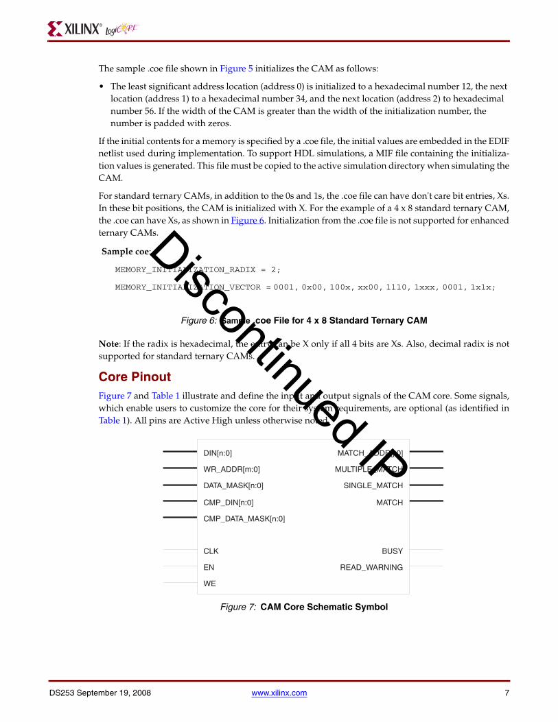
Core PinoutFigure 7 and Table 1 illustrate and define the input and output signals of the CAM core. Some signals,which enable users to customize the core for their system requirements, are optional (as identified inTable 1). All pins are Active High unless otherwise noted.
X-Ref Target - Figure 6ff
Figure 6: Sample .coe File for 4 x 8 Standard Ternary CAM
X-Ref Target - Figure 7
Figure 7: CAM Core Schematic Symbol
Sample coe:
MEMORY_INITIALIZATION_RADIX = 2;
MEMORY_INITIALIZATION_VECTOR = 0001, 0x00, 100x, xx00, 1110, 1xxx, 0001, 1x1x;
DIN[n:0]
WR_ADDR[m:0]
DATA_MASK[n:0]
CMP_DIN[n:0]
CMP_DATA_MASK[n:0]
CLK
EN
WE
MATCH_ADDR[j:0]
MULTIPLE_MATCH
SINGLE_MATCH
MATCH
BUSY
READ_WARNING
Discontinued IP

8 www.xilinx.com DS253 September 19, 2008
CLK (Clock)
The CAM module is fully synchronous with the rising edge of the clock input. All input pins havesetup time referenced to the CLK signal. All output ports have clock-to-out times referenced to the CLKsignal.
EN (Enable)
When active, the optional enable signal allows the CAM to execute write and read operations. If theenable is inactive during normal operation of the core, the output pins hold their previous state and allinternal states freeze. Any new input signal is ignored until the enable is driven active, at which timethe CAM resumes all of its halted operations.
Table 1: CAM Core Signals
Signal Name Direction Description
CLK InputClock: All CAM operations are synchronous to the rising edge of the clock input.
EN(Optional)
InputEnable: Control signal used to enable both write and read operation.
DIN [n:0] InputData In: Data to be written to CAM during write operation. Also, data to look up from the CAM during read operation, when simultaneous read/write option is not selected.
DATA_MASK [n:0](Optional)
InputData Mask: Interacts with the DIN bus to create new bit values in ternary mode.
CMP_DIN [n:0](Optional)
InputCompare Data In: Data to look up from the CAM during read operation if the simultaneous read/write option is selected.
CMP_DATA_MASK[n:0](Optional)
InputCompare Data Mask: This bus interacts with the CMP_DIN bus to create new bit values in ternary mode if the simultaneous read/write option is selected.
WE(Optional)
InputWrite Enable: Control signal used to enable transfer of data into CAM from the DIN bus.
WR_ADDR [m:0](Optional)
InputWrite Address: The location that the data on DIN will be written into the CAM.
BUSY OutputBusy: Indicates that write operation is currently being executed.
MATCH_ADDR [j:0] OutputMatch Address: CAM address where matching data resides.
MATCH OutputMatch: Indicates that least one location in the CAM contains the same data as the DIN bus (or CMP_DIN if in simultaneous read/write mode).
READ_WARNING(Optional)
OutputRead Warning: Indicates that the data applied to the CAM for a read operation matches the data that is currently being written into the CAM by the unfinished write operation.
MULTIPLE_MATCH(Optional)
OutputMultiple Match: Indicates existence of matching data in more than one location of the CAM.
SINGLE_MATCH(Optional)
OutputSingle Match: Indicates existence of matching data in only one location of the CAM.
Discontinued IP

DS253 September 19, 2008 www.xilinx.com 9
DIN[n:0] (Data In Bus)
The DIN bus provides the data to be written into or read from the CAM core, depending on the opera-tion. If the simultaneous read/write option is selected, this bus is used only for the write operation, andCMP_DIN bus is used exclusively for the read operation.
In enhanced ternary mode, this bus becomes one of the two input busses used to determine the bitvalue. A 0 on both DIN and DATA_MASK designates an X. A 1 on both busses designates a U. A 1 on DINand a 0 on DATA_MASK designates a 1. A 0 on DIN and a 1 on DATA_MASK designates a 0.
DATA_MASK[n:0] (Data In Mask Bus)
This optional input bus is available when one of the ternary modes is selected. In standard ternarymode, this signal masks the DIN bus to create the don’t care bits. Bits that are 1 on DATA_MASK indicatethe locations of the don't care bits on the DIN bus.
In enhanced ternary mode, this signal becomes one of the two input busses used to determine the bitvalue. For further information, see the description of DIN Bus defined in this section. This documenttreats the DATA_MASK bus as part of the DIN bus when a ternary CAM is selected.
CMP_DIN[n:0] (Compare Data In Bus)
When simultaneous read/write option is selected, this optional input bus provides the data for the readoperation of the CAM. When simultaneous read/write option is not selected, this bus is not available.
In enhanced ternary mode, this bus becomes one of the two input busses used to determine the bitvalue during a read operation. For further information, see the description of DIN Bus defined in thissection.
CMP_DATA_MASK[n:0] (Compare Data Mask)
This optional input bus is available when the CAM core is configured to support both simultaneousread and write operations and ternary mode. In standard ternary mode, this signal masks the CMP_DINbus to create don’t care bits. Bits that are 1 on this bus indicate the locations of don’t care bits on theCMP_DIN bus.
In enhanced ternary mode, this bus becomes one of the two input busses used to determine the bitvalue. For more information, see descriptions on DIN bus and DATA_MASK bus defined in this section.This document treats the CMP_DATA_MASK bus as part of the CMP_DIN bus when a ternary CAM isselected.
WE (Write Enable)
The optional write enable signal allows data on the DIN bus to be written into the CAM. When this sig-nal is asserted, the contents on the DIN bus are written into the location selected by the write addressbus WR_ADDR. This signal is not present if the read-only CAM option is selected. This signal isoptional when the CAM initialization option is selected.
WR_ADDR[m:0] (Write Address Bus)
The optional write address bus determines the memory location to be written to during the CAM'swrite operation. This bus is not present if the read-only CAM option is selected. This bus is optionalwhen the CAM initialization option is selected.
Discontinued IP

10 www.xilinx.com DS253 September 19, 2008
BUSY (Busy)
The busy signal indicates that the write operation is currently being executed. It remains asserted untilthe multiple clock cycle write operation is completed. The user cannot start a new write operationwhile this signal is active.
MATCH_ADDR[j:0] (Match Address Bus)
This output bus indicates the address that matches the contents of the DIN bus, or the CMP_DIN bus ifthe simultaneous read/write option is selected. Match address can be encoded (binary), single-matchunencoded (one-hot), or multiple-match unencoded.
MATCH (Match)
The match signal is asserted for one clock cycle when data on the DIN bus matches data in one or morelocations in the CAM. If simultaneous read/write option is selected, data on the CMP_DIN bus is usedto search for a match instead of the DIN bus.
READ_WARNING (Read Warning)
The optional read warning signal is asserted when data for the write in progress of the CAM is the sameas data for the read initiated for the CAM. Since write operations take multiple cycles, writes per-formed prior to reads may not have been completed when the read is executed. READ_WARNING isasserted to let the user know that the match address and match signals do not reflect the results of themost recent write operation being executed.
MULTIPLE_MATCH (Multiple Match)
The optional multiple match signal is asserted for one clock cycle when more than one match is presentin the CAM. It remains inactive if there is one or fewer matches.
SINGLE_MATCH (Single Match)
The optional single match signal is asserted for one clock cycle when there is only one match in theCAM. It remains inactive if there is more than one match, or if there are no matches.
Discontinued IP

DS253 September 19, 2008 www.xilinx.com 11
Generating the Core The CAM core, available through the CORE Generator software, provides two customization screens.To open the CAM core from the main CORE Generator window, click View by Function > Memories &Storage Elements > CAMs.
CORE Generator Parameter Screens
Two customization screens are available for customizing CAM parameters.
Screen 1
• Component Name. Select the base name of the output files generated for the core (up to 256 characters). Names must begin with a letter and be composed of any of the following characters: a to z, 0 to 9, and “_.” Verilog or VHDL reserved words cannot be used.
• Memory Type. Select either SRL16 or Block Memory. The SRL16 option implements a SRL16-based CAM, and the Block Memory option implements a Block SelectRAM-based CAM.
• Data Width. Enter the width of the data word to be stored in the CAM. The width value can be 1 to 512. Cores should not exceed the number of SRL16s or Block SelectRAM primitives available in the targeted device.
- Depth. Enter the number of words to be stored in the CAM. The depth value can be 16 to 4096. Cores should not exceed the number of SRL16s or Block SelectRAM primitives available in the targeted device.
X-Ref Target - Figure 8
Figure 8: CAM Parameters: Screen 1
Discontinued IP

12 www.xilinx.com DS253 September 19, 2008
• Match Address Type. Select one: Binary Encoded, Single-match Unencoded, or Multi-match Unencoded.
- Binary Encoded. Provides binary form of the matched address on the MATCH_ADDR bus. If more than one location exists in the CAM with matching data, either the lowest address or the highest address is driven on the MATCH_ADDR bus, depending on the selection of the Address Resolution type (see below).
- Single-match Unencoded. Provides decoded (one-hot) form of the matched address on the MATCH_ADDR. If this option is selected, width of the MATCH_ADDR bus equals the depth of the CAM and each bit on the MATCH_ADDR bus corresponds to a single location in the CAM. If more than one location exists in the CAM with matching data, either the lowest address or the highest address is driven on the MATCH_ADDR bus, depending on the selection of the Address Resolution type (see below).
- Multi-match Unencoded. Provides the decoded form of the matched addresses on the MATCH_ADDR bus for multiple address matches. If this option is selected, the width of the MATCH_ADDR bus equals the depth of the CAM and each bit on the MATCH_ADDR bus corresponds to a single location in the CAM. Each bit in the MATCH_ADDR bus with matching data is driven High.
• Ternary Mode. Select the Ternary Mode Off, Standard Ternary Mode, or Enhanced Ternary Mode option.
• COE File
- Load Initialization File. Select this option to activate the COE file option, an ASCII file with a .coe extension containing the initial contents of the CAM. For detailed information about the initial contents of the CAM, see Specifying CAM Contents.
- Read-Only CAM. Select this option for a Read-Only CAM; this option is only available when an initialization file (*.coe) is provided.
- Coefficient File Name. Displays the name of the .coe file loaded into the CAM. To browse for the .coe file, click Load Coefficients.
- Load Coefficients. Click to open a browser and select a .coe file.
- Show Coefficients. Click to open a window that displays the contents of the selected .coe file.
Note: The Load Initialization File functionality is only supported for binary and standard ternary CAMs and is not supported for enhanced ternary CAMs.
Discontinued IP

DS253 September 19, 2008 www.xilinx.com 13
Screen 2
• Additional Features
- Simultaneous Read/Write. Check the box to read and write on the same clock edge. Selecting this option separates the read and write data path. Data for the read operation uses the CMP_DIN bus and data for the write operation uses the DIN bus.
- Register Outputs. Available only in Block SelectRAM implementation. When selected, all match outputs are registered internally before being placed on the bus, adding one more clock cycle to the selected read latency. Selecting this option may eliminate timing problems that can be caused by large clock_to_out delays.
- Address Resolution. Select either Lowest or Highest. Available only when Binary Encoded or Single-Match address type is selected. Lowest option outputs the lowest matching CAM address; Highest option outputs the highest matching CAM address.
• Optional Pins
- Enable Pin. Select this option to include the EN port on the module; deselect the option to remove it.
- Single Match Flag. Select this option to include the SINGLE_MATCH port on the module; deselect the option remove it.
- Multiple Match Flag. Select this option to include the MULTIPLE_MATCH port on the module; deselect the option to remove it.
X-Ref Target - Figure 9
Figure 9: CAM Parameters: Screen 2
Discontinued IP

14 www.xilinx.com DS253 September 19, 2008
- Read Warning Flag. Select this option to include the READ_WARNING port on the module; deselect the option to remove it.
• Information
This non-enterable section displays a summary of the selected core options.
- Block Memory Used (Estimated). Displays the estimated number of block RAM primitives that will be used to construct the core. For Virtex-II (and its derivatives), Spartan-3 (and its derivatives), and Virtex-4, the number of 16k block RAMs is displayed. For Virtex-5 FPGAs, the number of 32k block RAMs is displayed
- SRL16Es Used (Estimated). Displays the estimated number of SRL16E primitives that will be used to construct the core.
- Read Latency (in clock cycles). Displays the number of clock cycles for a CAM read operation. For block RAM based CAMs, this value is controlled by the optional output register option.
- Write Latency (in clock cycles). Displays the number of clock cycles for a CAM write operation. For SRL16E based CAMs, the write latency is 16 clock cycles; for block RAM based CAMs, the write latency is 2 clock cycles.
Core ParametersFigure 2 defines the XCO parameters used to specify the configuration of the core. This parameter listapplies to users that generate the core using the CORE Generator GUI.
Table 2: Parameter File Information
Parameter Name Type/Value Default Setting
component_name string / up to 256 characters blank
memory_type “SRL16E” or “BLOCK” SRL16E
data_width integer / 1 to 512 8
depth integer / 16 to 4096 16
match_address_type“BINARY_ENCODED”“SINGLE_MATCH_UNENCODED”“MULTI_MATCH_UNENCODED”
BINARY_ENCODED
simultaneous_read_write “TRUE” or “FALSE” FALSE
register_outputs “TRUE” or “FALSE” FALSE
ternary_mode“TERNARY_MODE_OFF”, “TERNARY_MODE_STANDARD”, or “TERNARY_MODE_ENHANCED”(1)
TERMNARY_MODE_OFF
address_resolution “LOWEST” or “HIGHEST” LOWEST
enable “TRUE” or “FALSE” FALSE
read_warning_flag “TRUE” or “FALSE” FALSE
single_match_flag “TRUE” or “FALSE” FALSE
multiple_match_flag “TRUE” or “FALSE” FALSE
Discontinued IP

DS253 September 19, 2008 www.xilinx.com 15
Resource Utilization and Performance Examples
Block SelectRAM Memory Implementation
The number of Block SelectRAM primitives required depends on the CAM depth and width selectedon the CORE Generator screen.
SRL16 Implementation
The number of SRL16 primitives required depends on the depth and width of the CAM and on whethera ternary CAM is selected on the CORE Generator screen.
Resource Utilization and Performance BenchmarkingTo maximize clock frequency, use the following CAM configuration:
• Single-match Flag = FALSE
• Multiple-match Flag = FALSE
• Match Address Type = Multi-match Unencoded
This is recommended for CAMs with depths greater than 256 words. Clock frequency depends on thecore configuration.
Tables 3 and 4 show resource utilization and performance values for a 32-bit wide, 256-deep CAM forvarious match address types and storage element types implemented in a Virtex-5 device and a Spar-tan-3A device, respectively. These devices only contain a CAM and some glue logic and are thereforerepresentatives of ideal performance, rather than typical performance.
In the benchmark designs described in the tables that follow, the core was encased in a wrapper withinput and output registers to remove the effects of IO delays from the results; performance may varydepending on the design.
Benchmarks were performed targeting the slowest and the fastest speed grade devices in the Virtex-5and Spartan-3A FPGAs.
• For Virtex-5 FPGAs, XC5VLX220 -1 (slowest) and XC5VLX220 -2 (fastest)
• For Spartan-3A FPGAs, XC3S1400A -4 (slowest) and XC3S1400A -5 (fastest)
load_initialization_file “TRUE” or “FALSE” FALSE
coefficient_file string blank
read_only_cam “TRUE” or “FALSE” FALSE
1. CAM v4.0 and earlier used FALSE and TRUE for the ternary_mode parameter; CAM v5.0 and higher use TERNARY_MODE_OFF andTERNARY_MODE_STANDARD, respectively.
Table 2: Parameter File Information (Cont’d)
Parameter Name Type/Value Default Setting
Discontinued IP

16 www.xilinx.com DS253 September 19, 2008
Tables 5 and 6 show how CAM content size affects the resource utilization and performance in Virtex-5 and Spartan-3A devices. Tables 7 and 8 show how CAM content size affects resource usageand performance clock periods for block SelectRAM memory in Virtex-5 and Spartan-3A devices. Notethat these devices only contain a CAM and some glue logic and for this reason represent ideal perfor-mance rather than typical performance.
Table 3: Virtex-5FPGA CAM Implementation: Resource Utilization and Performance
Match Address Type
SRL16 Block RAM
SRL16s LUTs FFs Perf. (MHz)(1)
1. xc5vlx220, speed grade -1 (slowest)
Perf.(MHz)(2)
2. xc5vlx220, speed grade -2 (fastest)
Block RAMs LUTs FFs Perf.
(MHz)(1)Perf.
(MHz)(2)
Binary Encoded 2048 3438 60 100 110 32 1263 302 110 130
Single Match Unencoded 2048 3604 308 100 110 32 1405 302 100 120
Multi Match Unencoded 2048 3259 308 100 120 32 1144 303 110 130
Table 4: Spartan-3A FPGA CAM Implementation: Resource Utilization and Performance
Match Address Type
SRL16 Block RAM
SRL16 LUTs FFs Perf. (MHz)(1)
1. xc3s1400a, speed grade -4 (slowest)
Perf. (MHz)(2)
2. xc3s1400a, speed grade -5 (fastest)
Block RAMs LUTs FFs Perf.
(MHz)(1)Perf.
(MHz)(2)
Binary Encoded 2048 3333 60 50 60 32 2236 303 60 70
Single Match Unencoded 2048 3430 309 50 60 32 2372 303 50 60
Multi Match Unencoded 2048 3336 309 50 60 32 2176 303 50 60
Table 5: Virtex-5 FPGA SRL-based CAM Implementation: Resource Utilization and Performance
CAM Width
CAM Depth
16 256 1024
SRL16s LUTs FFs Perf. (MHz)(1)
1. xcv5vlx220, speed grade -1 (slowest)
Perf. (MHz)(2)
2. xcv5vlx220, speed grade -2 (fastest)
SRL16s LUTs FFs Perf.(MHz)(1)
Perf. (MHz)(2) SRL16s LUTs FFs Perf.
(MHz)(1)Perf.
(MHz)(2)
8 32 148 27 190 200 512 1848 36 110 120 2048 7200 39 80 100
32 128 288 52 170 200 2048 3438 60 100 110 8192 13493 63 70 80
64 256 474 84 160 190 4096 5561 93 90 100 16348 21899 101 60 70
Discontinued IP

DS253 September 19, 2008 www.xilinx.com 17
Table 6: Spartan-3A FPGA SRL-based CAM Implementation: Resource Utilization and Performance
CAM Width
CAM Depth
16 256 1024
SRL16s LUTs FFs Perf. (MHz)(1)
1. xc3s1400a, speed grade -4 (slowest)
Perf. (MHz)(2)
2. xc3s1400a, speed grade -5 (fastest)
SRL16s LUTs FFs Perf.(MHz)(1)
Perf. (MHz)(2) SRL16s LUTs FFs Perf.
(MHz)(1)Perf.
(MHz)(2)
8 32 151 27 80 100 512 1727 36 50 70 2048 6646 42 40 50
32 128 299 52 80 100 2048 3333 60 50 60 8192 12892 66 40 40
64 256 499 84 80 90 4096 5464 92 40 50 *(3)
3. Does not fit in an xc3s1400a device
*(3) *(3) *(3) *(3)
Table 7: Virtex-5 FPGA Block RAM-based CAM Implementation: Resource Utilization and Performance
CAM Width
CAM Depth
16 256 1024
Block RAMs LUTs FFs Perf.
(MHz)(1)
1. xc5vlx220, speed grade -1 (slowest)
Perf. (MHz)(2)
2. xc5vlx220, speed grade -2 (fastest)
Block RAMS LUTs FFs Perf.
(MHz)(1)Perf.
(MHz)(2)Block RAMs LUTs FFs Perf.
(MHz)(1)Perf.
(MHz)(2)
8 1 95 34 200 210 8 1077 277 130 160 32 4138 1048 100 110
32 4 170 57 170 180 32 1263 302 110 130 128 4677 1072 60 80
64 7 281 91 140 160 56 1721 335 90 110 *(3)
3. Does not fit in the available block RAMs for an xc5vlx220 device
*(3) *(3) *(3) *(3)
Table 8: Spartan-3AFPGA Block RAM-based CAM Implementation: Resource Utilization and Performance
CAM Width
CAM Depth
16 256 1024
Block RAMs LUTs FFs Perf.
(MHz)(1)
1. xc3s1400a, speed grade -4 (slowest)
Perf. (MHz)(2)
2. xc3s1400a, speed grade -5 (fastest)
Block RAMS LUTs FFs Perf.
(MHz)(1)Perf.
(MHz)(2)Block RAMs LUTs FFs Perf.
(MHz)(1)Perf.
(MHz)(2)
8 1 124 35 110 130 8 1368 278 70 80 32 5623 1079 50 60
32 4 219 59 90 120 32 2236 303 60 70 *(3)
3. Does not fit in the available block RAMs for an xc3s1400a device
*(3) *(3) *(3) *(3)
64 8 357 92 90 110 *(3) *(3) *(3) *(3) *(3) *(3) *(3) *(3) *(3) *(3)
Discontinued IP

18 www.xilinx.com DS253 September 19, 2008
Tables 9 and 10 show the resource usage and performance in Virtex-5 and Spartan-3A devices for a 32-bit wide and 256-words deep CAM using a multiple match unencoded match address type withother configuration options turned on.
Ordering InformationThe CAM core may be downloaded from the Xilinx IP Center for use with the Xilinx CORE Generatorsystem v10.1 and higher. The Xilinx CORE Generator system is bundled with the ISE software packageat no additional charge. Information about additional Xilinx LogiCORE IP modules is available on theXilinx IP Center.
To order Xilinx software, please visit the Xilinx Online Store or contact your local Xilinx sales represe-sentative.
Revision HistoryThe following table shows the revision history for this document.
Table 9: Virtex-5 FPGA CAM Implementation: Resource Utilization and Performance
Options
SRL16 Block RAM
SRL16s LUTs FFsPerf.
(MHz)(1)
1. xc5vlx220, speed grade -1 (slowest)
Perf. (MHz)(2)
2. xc5vlx220, speed grade -2 (fastest)
Block RAMs
LUTs FFsPerf.
(MHz)(1)Perf.
(MHz)(2)
Single Match Multiple Match Flags On
2048 3259 308 100 120 32 1144 303 110 130
Ternary Mode On 4096 5623 341 80 100 N/A(3)
3. Ternary mode not supported for block RAM based CAMs.
N/A(3) N/A(3) N/A(3) N/A(4)
Registered Outputs N/A(4)
4. Registered Outputs not supported for SRL based CAMs.
N/A(4) N/A(4) N/A(4) N/A(4) 32 1144 562 110 130
Table 10: Spartan-3A FPGA CAM Implementation: Resource Utilization and Performance
Options
SRL16 Block RAM
SRL16s LUTs FFs Perf. (MHz)(1)
1. xc3s1400a, speed grade -4 (slowest)
Perf. (MHz)(2)
2. xc3s1400a, speed grade -5 (fastest)
Block RAMs LUTs FFs Perf.
(MHz)(1)Perf.
(MHz)(2)
Single Match Multiple Match Flags On 2048 3336 309 50 60 32 2176 303 50 60
Ternary Mode On 4096 5676 341 40 50 N/A(3)
3. Ternary mode not supported for block RAM based CAMs.
N/A(3) N/A(3) N/A(3) N/A(3)
Registered Outputs N/A(4)
4. Registered Outputs not supported for SRL based CAMs.
N/A(4) N/A(4) N/A(4) N/A(4) 32 2265 561 60 70
Date Version Revision
03/28/03 1.0 Revision history added to the document.
04/28/04 2.0 Updated document to support CAM core v5.0.
11/11/04 2.1 Updated document to indicate support of Xilinx CORE Generator v6.3i.
9/19/08 3.0 Support for Virtex-5 and Spartan-3A/3A DSP FPGAs.
Discontinued IP