xcvr d i t i ixcvr design training - · pdf filexcvr d i t i ixcvr design training ... sendi...
TRANSCRIPT

XCVR D i T i iXCVR Design Training
P t S h Hi h S d S i li tPeter Schepers High Speed SpecialistNovember 2012
© 2012 Altera Corporation—Public

Agenda Transceiver Architecture Clock Recovery and Jitter Tracking Clock Recovery and Jitter Tracking Transmitter PLL
Transceiver Design Transceiver Design Transceiver Reconfiguration
f Demo Design Using Reconfiguration Signal Conditioning and Best Practices for Link
T i iTraining Signal Integrity Simulation (with Demo) Transceiver Toolkit (with Demo)
© 2012 Altera Corporation Public

Transceiver Design Trends & Challenges
Data ratesSystem integration
Optical modulesBackplanes Backplanes
Statistical reliability Low jitter og
Sca
le
1000
PCI 2PCIe 3j
Bit Error Ratio (BER)
Design productivity
dth
(Gbp
s) in
Lo
10
100
PCI X
PCIe
PCIe 2
8 G FCRapidIO 2.0
10 GbE4 G FC
InterlakenOC 768
100 GbERapidIO 3.0
Lower power consumptionBa
ndw
id1
10
1990 1995 2000 2005 2010PCI
PCI-66
PCI-X
1G FC
RapidIO 1.0
GbE
OC 48
10 GbE
3G-SDI
Altera’s innovation address the challenges of next generation transceiver design
© 2012 Altera Corporation Public
transceiver design
6

T i A hit tTransceiver Architecture
© 2012 Altera Corporation—Public

What is a Transceiver?
Combination transmitter/receiver used when di hi h d di it l d t / t l i lsending high-speed digital data/control signals
across physical mediumBoard traces Board traces
Backplane Optical fiber CAT5 cable
Used in the PHY (physical) layer of the OSI d lmodel
Made up of the physical coding sub-layer and h i l di tt h tphysical medium attachment
© 2012 Altera Corporation Public8

Serial Communication
Tx Channel R
PLL
DataChannel
D Q Data out
Rx
PLL
CPLL/CRU
Ref clock
Ref clock
© 2012 Altera Corporation Public9
Ref clock

What are transceivers
Tx parallel data
Tx parallel clk
pll_ref_clk
Rx parallel data
Rx parallel clk
transmit and receive parallel data on a serial link
© 2012 Altera Corporation Public10

Definitions
Media Access Controller (MAC)A bl k t t b t itt d li k Assembles packets to be transmitted across link
Disassembles packets received from across link Handles error and fault messages from link
Physical Coding Sub-Layer (PCS) Digital logic that prepares and formats data for transmission across a
physical medium type or restores received data to original formphysical medium type or restores received data to original form Detects link errors Ex. Encoding, decoding, scrambling, descrambling
Physical Medium Attachment (PMA) Converts digital data to serial analog stream or reverse
Connects to physical medium Connects to physical medium Ex. Parallel to serial conversion
© 2012 Altera Corporation Public11

28-nm Device Families
Cyclone V Arria V Stratix V Stratix V
© 2012 Altera Corporation Public12

Cyclone V FPGA FamilyOpening Up
Design Cyclone V FPGA Family es gPossibilities
Lowest cost and power 3G transceivers 5G transceivers
Optimized for Optimized forplowest system cost and power
for a wide
Optimized for lowest cost and power for 614 Mbps to 3 125
FPGA industry’s lowest cost and power for 5.0
spectrum of general logic and DSP applications
Mbps to 3.125 Gbps transceiver
applications
Gbps transceiver applications
FPGA E Variant GX Variant GT Variant
IntegratedARM Corte A9ARM Cortex-A9 MPCore Processor System
SE Variant SX Variant ST Variant
© 2012 Altera Corporation Public13

Arria V FPGAs
Lowest power 6G and 10G FPGAsAdaptive logic modules (ALMs)
Variable-precision digital signal processing (DSP) blocksM10K embedded memory blocks
Distributed memory logic array blocks (MLABs)Distributed memory logic array blocks (MLABs) PCI Express® (PCIe®) Gen1 and Gen2
Hard multiport memory controller
With 6G transceivers With 10G transceivers With Integrated ARM Cortex-A9 MPCore
Processor System
© 2012 Altera Corporation Public14
Processor System

Stratix V Device Family Variants
Stratix V E variantF hi h t d it hi h f For highest density, high-performance applications
Stratix V GS variant28 Gb
Optimized for high-performance, high-precision DSP applications with transceivers up to 14.1 Gbps
28-GbpsTransceivers
p p
Stratix V GX variant Up to 66 transceivers at 14.1 Gbps for high
performance, high bandwidth
Stratix V GT variant 28 Gb f hi h f Variable-Precision 28 Gbps for high-performance, ultra-high bandwidth applications
Variable-PrecisionDSP Block
© 2012 Altera Corporation Public

Transceiver Locations
Stratix V GX device with 36 full transceiver
h lchannelsXCVR BANK
XCVR BANK
Cyclone V GX device XCVR BANK
XCVR BANK
Cyclone V GX device with 12 full transceiver
channelsXCVR BANK
PCIe
PCIeHIP
PCIe
XCVR BANK
XCVR BANK
XCVR BANK
HIPPCIeHIP
HIP
© 2012 Altera Corporation Public16

Transceiver LayoutStratix V GX device with
36 full transceiver h lchannels
XCVR BANK
XCVR BANK
XCVR BANK
XCVR BANK
PCIePCIe TX4 & RX4
TX5 & RX5
3 bank
PLL
PLL
XCVR BANK
XCVR BANK
HIPHIPTX3 & RX3
TX2 & RX2
6 bank
PLL
PLL
TX1 & RX13 bank
PLL
TX0 & RX0 PLL
© 2012 Altera Corporation Public17

Standard PCS Datapath
© 2012 Altera Corporation Public

Tx CHANNEL
TX FIF O
Fram
eG
en
CRC
32G
en
64B/
66B
Enc.
+TX
SM
S cr a
mb l
er
Dis
p ar it
yG
en TXGe
arbo
x+
Bit s
lip
PRBSGen
Rep. Pat G
PRPGen
tx_pld_clkGen
tx_pma_clktx_clk_out
RXG
earb
o x+
Bit s
lip
Fram
eS y
n c
Blk
syn c
Dis
p ar it
yCh
k
De-
S cr a
mb l
er
CRC
32Ch
k
64B/
66B
Dec.
+RX
SM
RX F IF O
PRBSVer
PRPVer
BERrx pma clkrx_pld_clk rx_pma_clk
rx_clk_out
Rx CHANNEL10G PCS Interlaken
10G Ethernet
© 2012 Altera Corporation Public19

PCI-Express Hard-IP
Stratix V PCIe Gen 3/2/1 x8 HIP with 256 bit architecturearchitecture
New Stratix V PCIe Gen3 32-bit PCS used with HIP Implements the 128/130 bit encoding/decoding scheme
C fi ti i Configuration via PCI-Express (CvPCIe) enabled i thi bl k
8GPCSin this block
Software/driver modelPlug-and-play model
Application
PCS
10G
20
xpre
ss H
IP
Data integrity
Protocol Transaction
Data link
PLD10GPCS
PMA
40
PCI-E
x
Point-to-point, serial, differential,hot-plug, multiple form factors
g y
Physical PCI-express PCS/Hard-IP
32
© 2012 Altera Corporation Public20

Clock Recovery andClock Recovery andJitter Tracking
© 2012 Altera Corporation—Public

HSIO Link Architecture Advancement PathHSIO Link Architecture Advancement PathHSIO Link Architecture Advancement PathHSIO Link Architecture Advancement Path
1 Gb 56 Gb
Tx Rx
1 Gbps – 56 Gbpsclock embedded in coded data
ta ra
te
~0 1 Gbps
~0.8 Gbpssource synchronized
Tx RxCoded data
Gigabit EthernetCEI/OIF
Dat ~0.1 Gbps
global clock
Tx RxTx Rx
Strobe
Data
PCI Express40G/100G Ethernet …..
Data
Clock
Time
Clock
© 2012 Altera Corporation Public22

Serial Data Communication SystemU i T iUsing a Transceiver
Ch l
DataC
Q
Channel
DataD
Clock/PLL CR/PLL
Transmitter Receiver
HL(f)
de (d
B)
Frequency (f)fc
Mag
nitu
© 2012 Altera Corporation Public23
eque cy ( )fc

Clock and Data Recovery (CDR)
CDR has lock-to-clock and lock-to-data modes CDR is first locked to the reference clock then switched to lock the data providing fast CDR is first locked to the reference clock, then switched to lock the data, providing fast
locking time No unlocked or out-of-lock problems when the received data has excessive jitter Reference clock jitter does not affect CDR jitter performance
© 2012 Altera Corporation Public24
j j p

The importance of a high bandwidth
© 2012 Altera Corporation Public25

Jitter and Reference Clock
What matters in a link system is the relative jitter referenced to the recovered clockrecovered clock
The net jitter is the phase difference between the data and the recovered clock
Data phase
Recovered clock phase
hase
Difference
Ph
0 Difference
Time
0
© 2012 Altera Corporation Public26

Jitter Transfer Function
H (s) H (s) = 1 H (s)HL(s)from CR/PLL
HH(s) = 1-HL(s)from difference function
HH(f)tu
de (d
B) HH(f)
Mag
ni
Frequency (f)fc
© 2012 Altera Corporation Public27

Jitter Tolerance Function
H (f) jitt t lHT(f) jitter tolerance
(dB
)ag
nitu
de (
HH(f): jitter transfer
Ma
Frequency (f)fc
Higher fc, better jitter tracking, better jitter tolerance
© 2012 Altera Corporation Public28

Jitter Tolerance Comparison<-40 dB/decade
Mag
nitu
de
PLL/hybrid CR-20 dB/decade
M y
PI CR
FrequencyfPLLfPl
Receivers have a hybrid phase-locked loop (PLL)-based CDR technology that has the best jitter generation and jitter tolerance performance
q yPLLPl
© 2012 Altera Corporation Public29

The proof !
© 2012 Altera Corporation Public30

T itt PLLTransmitter PLL
© 2012 Altera Corporation—Public

Transmit Clocking Options Clocking options enabling independent
data rates and flexible clock distribution ATX (LC)CMU
T it PLL D t R B fit
network ATX PLL (LC)
Wider operating range enabled by different
CMUfPLL
Transmit PLL option
Data Range (Gbps)
Benefit
ATX (LC) PLL 1 – 14.1 Best jitter performance
p g g yVCO modes
Sub-picoseconds of jitter for high statistical reliability
Cl k M t U it (CMU) performance
CMU (Ring Oscillator) 0.6 – 12.5 Best data-rate
range
Additional PLL
Clock Management Unit (CMU) Ring Oscillator for continuous operating range
with best in class jitter
fPLLs can be used for transceivers in fPLL 0.6 – 3.75 Additional PLL source
fPLLs can be used for transceivers in addition to general device clocking
Up to 44 independent 12.5Gbps channels on a single Stratix V FPGA
© 2012 Altera Corporation Public32
single Stratix V FPGA

CMU PLL Operating Range Each channel can be configured as data channel
or as CMU (clock management for the transmit PLL)Hard PCS Transceiver PMA
ck
Similar CMU to Stratix IV - Ring-oscillator Wide operating range with low transmit jitter
0.6Gbps – 12.5GbpsClo
ck n
etw
orks
Hard PCS
Hard PCS
Hard PCS
Hard PCS Transceiver PMA
Transceiver PMA
PMA/CMU
Transceiver PMAC T
rans
mit
PLLs
dded
Har
dCop
y B
loc
actio
nal P
LLs
(fPLL
)
Hard PCS
Hard PCS
Transceiver PMA
Transceiver PMA
L
Embe
dFr
a
CMU PLLData Rate(Gbps)12 50 6
© 2012 Altera Corporation Public33
( p )12.50.6

CMU PLL
If you use Channel PLL as CMU PLL the RX is unavailable (no CDR)
© 2012 Altera Corporation Public

CMU PLLs
CMU PLLs in channels 1 and 4 in 6 transceiver bank can generate clocks for other transceiver channels within or
t id t i b k
Ch 5
Ch 4 outside transceiver bank CMU PLL channel may still be used
TX l h l
Ch 4
Ch 3as TX-only channel
Ch 2
Ch 1Ch 1(CMU PLL)
Ch 0
© 2012 Altera Corporation Public35

Programmable ATX PLL 1 ATX PLL / 3 channels (triplet) Sub-picoseconds jitter achieved with LC PLLHard PCS Transceiver PMA
ck
p j Programmable ATX (LC) PLL Range
8 Gbps - 14.1 Gbps 4 Gbps – 7.05 GbpsC
lock
net
wor
ks
Hard PCS
Hard PCS
Hard PCS
Hard PCS Transceiver PMA
Transceiver PMA
Transceiver PMA
Transceiver PMAC T
rans
mit
PLLs
dded
Har
dCop
y B
loc
actio
nal P
LLs
(fPLL
)
2 Gbps – 3.525 Gbps 1 Gbps – 1.7625 Gbps (using local divider)
Hard PCS
Hard PCS
Transceiver PMA
Transceiver PMA
L
Embe
dFr
a
PFD CP / LF
LCVCO0
/LDiff Ref -Clock input
outputdiv/2
LCVCO1 div/2
/M/M
Data Rate(Gbps)14 11 00 6 87 0541 8 2 3 25
© 2012 Altera Corporation Public36
( p )14.11.00.6 87.0541.8 2 3.25

Stratix V ATX PLLs
Better jitter performance at higher d h CMU PLLdata rates than CMU PLLs
Limited frequency supportATX
Ch 5
Ch 4 Must be tuned to support a target data
range
Two per 6 transceiver bank
PLLCh 4
Ch 3 Two per 6-transceiver bank Allow full use of device
transceiver channelsATX
Ch 2
Ch 1 transceiver channels Channel PLL can be used as CDR PLL
Stratix V GT (28G) channels must
ATX PLL
Ch 1
Ch 0 Stratix V GT (28G) channels must
use ATX PLLs
© 2012 Altera Corporation Public37

Fractional PLL (fPLL) When used as transmit PLL
0.6Gbps – 3.25Gbps1 fPLL / 3 channels
Hard PCS Transceiver PMA
ck 1 fPLL / 3 channels Integer mode only
Clo
ck n
etw
orks
Hard PCS
Hard PCS
Hard PCS
Hard PCS Transceiver PMA
Transceiver PMA
Transceiver PMA
Transceiver PMAC T
rans
mit
PLLs
dded
Har
dCop
y B
loc
actio
nal P
LLs
(fPLL
)
PhaseFrequency
Detect
Divby N
ChargePump
LowPassFilter
VCO Divby C
Hard PCS
Hard PCS
Transceiver PMA
Transceiver PMA
L
Embe
dFr
a
MultipleModulusDivider
DeltaSigma
Modulator
Stratix V fPLL block diagramStratix V fPLL block diagram
Data Rate(Gbps)14 13 250 6
fPLL used as transmit PLL
© 2012 Altera Corporation Public38
( p )14.13.250.6

Fractional PLLs
Can serve directly as t itt PLLtransmitter PLL Data rate dependant
Provide increasedfPLL
Ch 5
Ch 4 Provide increased multiplication/division factors over CMU PLLs
fPLLCh 4
Ch 3
Allows full use of device transceiver channels
Ch 2
Ch 1 fPLL Channel PLL can be used as CDR PLLCh 1
Ch 0
fPLL
© 2012 Altera Corporation Public39

Other use of Fractional PLLs
Supported in Stratix V and A i VArria V
Generate reference clock for channel/ATX PLLsATX
Ch 5
Ch 4 fPLL channel/ATX PLLs Provide increased
multiplication/division factors
PLLCh 4
Ch 3
fPLL
multiplication/division factors Support using a reference clock
frequency not directly supported by channel/ATX PLLsATX
Ch 2
Ch 1 fPLL channel/ATX PLLs
Drive reference clock lines that span the sides of FPGA
ATX PLL
Ch 1
Ch 0
fPLL
p Can be segmented per transceiver bank
© 2012 Altera Corporation Public40

Transmitter Local Clock Dividers
One in each channel Receive high speed
serial clocks from any transmitter PLLtransmitter PLL
Generates High-speed serial clock for local g p
PMA Low-speed parallel clock for local
PMA/PCS
Active in non-bonded(x1) mode
Each channel divides high- Each channel divides high-speed clock to support its individual target data rate
© 2012 Altera Corporation Public41

Central Clock Dividers
Special functionality of local Ch5Local Clock Divider
clock dividers in channels 1 and 4 of transceiver bank
Ch4
Local Clock Divider
Local Clock Divider
Each central clock divider can generate high-speed
Ch3Local Clock Divider g g p
serial AND low-speed parallel clocks for bonded
Ch2Local Clock Divider p
channelsCh1Central Clock Divider
Ch0Local Clock Divider
High-speed serial clockLow-speed parallel clock
© 2012 Altera Corporation Public42

T i D iTransceiver Design
© 2012 Altera Corporation—Public

Transceiver PHY IP Cores
Set of IP Cores that enable/configure the FPGAs PCS/PMA layers for high-speed designs
Both protocol-specific and generic cores p p gavailable
Implementation Implementation Embedded transceivers Core logic Both
© 2012 Altera Corporation Public44

Protocol-Specific PHY IP Cores
10GBASE-R 10GBASE-KR XAUI XAUI Interlaken
PHY IP f PCI E PHY IP core for PCI Express Hard IP for PCI Express …
© 2012 Altera Corporation Public45

Non-Protocol-Specific PHY IP Cores
Custom Low Latency Deterministic Deterministic Native PHY
© 2012 Altera Corporation Public46

Custom PHY IP
OverviewProvides all PCS blocks Provides all PCS blocks
Available only for the Standard PCS Alway includes Phase Compensation Fifo
Generic PHY for supporting custom interfaces Proprietary protocol No protocol-specific PHY IP available
PCS PMA
Phase Compensation
FIFO
Serdes8b / 10b Rate MatchFIFO
Word Aligner
Byte Ordering
Excellent for custom / proprietary protocols!
© 2012 Altera Corporation Public47

Custom PHY IP Parameter Editor (1)
© 2012 Altera Corporation Public48

Custom PHY IP Parameter Editor (2)
© 2012 Altera Corporation Public49

Low Latency PHY IP Core
Generic PHY for implementing low latency configurations in Stratix V transceiversin Stratix V transceivers Protocols/interfaces where specific PCS functionality not available and/or
designer wants lowest datapath latency
PCS f ti lit t b i l t d i th FPGA PCS functionality must be implemented in the FPGA core Contains
PMA and minimal (or no) PCSPMA and minimal (or no) PCS PMA and PCS register map Reset controller (optional) PHY management interfacePHY management interface
Supported devices, PCS configurations and data rates Stratix V Low-Latency PCS : 1 – 14.1 Gbps
All t l ifi bl k b d All protocol-specific blocks bypassed Stratix V GT PMA Direct: 20 – 28 Gbps
© 2012 Altera Corporation Public50

Low Latency PHY IP
Overview Provides a simple and a low latency path through the PCS Both the Standard and 10G PCS available
PCS PMA
Phase Compensation
FIFO
Serdes
Excellent for custom / proprietary protocols!Excellent for custom / proprietary protocols!
© 2012 Altera Corporation Public51

Low Latency PHY IP Parameter Editor
© 2012 Altera Corporation Public52

Deterministic PHY
Overviewknown timing for the transmit (TX) and receive (RX) datapaths known timing for the transmit (TX) and receive (RX) datapaths
Phase comp fifo in register mode Supports
Auto Rate Configuration Auto-Rate Configuration User initiated via Reconfiguration Controller
Support all CPRI/OBSAI data rates in 8G Hard PCS CPRI – 614.4Mbps to 9.8304Gbps OBSAI – 768Mbps to 6.144Gbps
© 2012 Altera Corporation Public53

Deterministic PHY IP Parameter Editor
© 2012 Altera Corporation Public54

Custom/Low Latency/Deterministic PHY IP Block Diagram
tx_serial_datarx serial data Serial DataAvalon-ST RX/TX tx_*
rx * rx_serial_datarx_
tx_readyrx_ready
pll lockedPCS/PMAControl & Statuspll ref clk pll_locked
…Control & Status
reconfig_* Reconfiguration
pll_ref_clk*_coreclkinClocks
phy_mgmt_*Avalon®-MMPHY Management
pll_powerdown*_analogreset* digitalreset
Reset Control & Status (Optional)_digitalreset
© 2012 Altera Corporation Public55

Custom/Low Latency/Deterministic PHY IP Interfaces Clock interfaces
To reference clock sources To MAC To any additional PCS blocks implemented in FPGA (as needed)To any additional PCS blocks implemented in FPGA (as needed)
Avalon-ST TX/RX interfaces – to MAC or user logic Serial data interface – to external channel Avalon-MM PHY management interface – to MAC or
PCS/PMA control logicT i fi ti i t f t Transceiver reconfiguration interface – to reconfiguration controller
Reset control and status – reset control logic Reset control and status reset control logic PCS/PMA control and status (optional) – to MAC or
PHY control logic
© 2012 Altera Corporation Public56

Clock Interfaces
pll_ref_clk: Input reference clock(s) tx_clkout: Output clock from PHY to use for
synchronizing TX output data, control and status i lsignals
rx_clkout: Output clock from PHY; synchronized t RX d t t l d t t i lto RX data, control and status signals
tx_coreclkin: Optional write-side transmitter h ti FIFO i t l kphase compensation FIFO input clock
rx_coreclkin: Optional read-side receiver phase ti FIFO i t l kcompensation FIFO input clock
© 2012 Altera Corporation Public57

Avalon-ST Input/Ouput Interfaces
Connects MAC to Custom PHY IP core Implements simple Avalon-ST interface with no
backpressure or latencyI t f i l d t d/ i d t Interface is always ready to send/receive data
Logic must be ready to send/receive as soon as reset is complete
Transmit signals Transmit signals tx_parallel_data: Outgoing input data to PHY
Receive signals Receive signals rx_parallel_data: Incoming output data from PHY
© 2012 Altera Corporation Public58
* For more information on the Avalon specification, please see the Avalon Interface Specification .

Serial Interface
Connects transmitter data output(s) and receiver data input(s) to external serial interface Backplane Physical medium dependent (PMD) interface Another FPGA
Signals Signals tx_serial_data: Transmitter data output
rx serial data: Receiver data input rx_serial_data: Receiver data input
© 2012 Altera Corporation Public59

PHY Management Interface
Provides a memory-mapped register space used to accessaccess PCS/PMA control and status registers Reset control registers Transceiver reconfiguration registersg g
Avalon-MM standard interface 32-bit data, 9-bit address32 bit data, 9 bit address Use read/write transactions to access register space
Example control/status registersExample control/status registers PLL locked status Reset RX/TX channel Bit/byte reversal Manual Wordalignment FIFO overflow/underflow
© 2012 Altera Corporation Public60
Note: See Altera Transceiver PHY IP Core User Guilde for register mapping.

PHY Management Avalon Write Transaction
phy_mgmt_write should be asserted for one clock cycle, because phy mgmt waitrequest is de asserted
At rising edge of phy_mgmt_clk, provide phy_mgmt_ address[8:0], phy mgmt writedata[31:0] and assert phy mgmt write
because phy_mgmt_waitrequest is de-asserted
phy_mgmt_writedata[31:0] and assert phy_mgmt_write Hold these values until PHY IP de-asserts phy_mgmt_waitrequest PHY IP captures phy_mgmt_writedata[31:0], de-asserts
phy mgmt waitrequest and ends the transfer
© 2012 Altera Corporation Public
phy_mgmt_waitrequest and ends the transfer
61

PHY Management Avalon Read Transaction
phy mgmt read should be asserted for 2 clock cycles,
At rising edge of phy_mgmt_clk, provide phy_mgmt_address[8:0] and assert phy mgmt read
p y_ g _ y ,because phy_mgmt_waitrequest is asserted
and assert phy_mgmt_read Hold these values until PHY IP de-asserts phy_mgmt_waitrequest PHY IP presents valid phy_mgmt_readdata[31:0] and de-asserts
phy mgmt waitrequest
© 2012 Altera Corporation Public
phy_mgmt_waitrequest
62

Reset Control & Status Interfaces
Embedded reset controller enabled phy_mgmt_clk_reset (Avalon-MM inteface): initiates reset of PHY tx_ready: PHY has exited reset and is ready to transmit data
rx ready: PHY has exited reset and is ready to receive data rx_ready: PHY has exited reset and is ready to receive data
Embedded reset controller disabled Embedded reset controller disabled PHY provides signals to connect Transceiver PHY Reset
Controller IP core or user-designed reset controllerg See device handbook for reset timing diagrams
Examplesll d R t TX PLL pll_powerdown : Resets TX PLL
tx_cal_busy: Indicates transmit channel is being calibrated rx_analogreset : Resets the RX PLL (CDR)
© 2012 Altera Corporation Public
tx_digitalreset : Resets the TX PCS blocks
63

Optional PCS/PMA Control and Status Interface Additional signals to determine and control state of g
PCS/PMA Provides instantaneous interaction over using PHY
management interfacemanagement interface Examples
tx datak: Input to indicate data/control code (8B/10B encoding bl d)
_ p ( genabled)
rx_syncstatus : Indicates single-lane word alignment rx_rmfifodatainserted : Indicates Rate Match has inserted skip
charactercharacter rx_errdetect : Indicates an 8B/10B code violation or disperity error
has occurredtx rlv: Indicates a run length violation has occurred in the receiver tx_rlv: Indicates a run length violation has occurred in the receiver
rx_datak: Data/control code indicator (8B/10B decoding enabled) rx_runningdisp: Indicates disparity of incoming data (8B/10B
decoding enabled)
© 2012 Altera Corporation Public
rx_enabyteordflag: Triggers byte ordering
64

Native PHY
Give control back to the user
First IP offering is always a family specific “Native” PHY IP. Lower level than PHY IP and altgx. Nothing but the ports and parameters No embedded reset controller no AVMMNothing but the ports and parameters. No embedded reset controller, no AVMM
CSR, no fPLLs, etc.
Protocol specific PHY IP when it makes sense. PIPE, Interlaken, 10GBase-KR, XAUI are good examples.
ScheduleSc edu e 12.0 Direct Mode (only PMA)
Reset controller as a separate optional IP 12.1 Full PCS Support:
Megawizard performs validation and provides feedback for all interfaces and parameters Megawizard performs validation and provides feedback for all interfaces and parameters. Megawizard gives warnings rather than errors when rules are violated.
© 2012 Altera Corporation Public

Stratix V Native PHY
GUIP d b f i l bl k (8B/10B d Parameters are grouped by functional block (8B/10B, word aligner, etc.)
Order matches the order from the PCS diagram
HDL Parameters and ports names are intended to be self explanatory: Parameter naming convention:
Standard(8G) PCS – std_rx_<param>, std_tx_<param> 10G PCS – teng_rx_<param>, teng_tx_<param>g_ _ p g_ _ p
Port naming convention Standard(8G) PCS – tx_std_..., rx_std_... 10G PCS – tx 10g rx 10g 10G PCS tx_10g_..., rx_10g_... PMA – tx_pma_..., rx_pma_...
© 2012 Altera Corporation Public66

Native PHY IP Cores
All PHY control/status signals exposed as ports Similar to enabling “all optional ports” on other PHY IP cores No memory-mapped register interface to control and monitor PHY
Must build own “register space” using ports to access in memory Must build own “register-space” using ports to access in memory-mapped system (if required)
Contains PHY (PCS/PMA) only Contains PHY (PCS/PMA) only Reconfiguration controller must be connected manually Reset controller must be connected manuallyy
Designer can use Transceiver PHY Reset Controller IP core or create own reset controller
© 2012 Altera Corporation Public67
* Other modes enabled in a future version of the Quartus II software

Native PHY
© 2012 Altera Corporation Public68

PMA GUI
© 2012 Altera Corporation Public69

Standard PCS
© 2012 Altera Corporation Public70

Standard PCS parameters
© 2012 Altera Corporation Public71

10G PCS – Parameter groups
© 2012 Altera Corporation Public72

10G PCS parameters
© 2012 Altera Corporation Public73

PHY IP Output Files for Compilation
<phy_instance_name>.qipS i t fil th t i t t ll fil d d f th i Script file that points to all files needed for synthesis
Add file to Quartus II project
<phy instance name>.v/.vhdphy_instance_name .v/.vhd Wrapper file that instantiates and configures the PHY IP core
megafunction
<ph instance name> folder <phy_instance_name> folder Combination of Verilog and SystemVerilog files representing PHY IP
core components <phy_instance_name>.ppf
Stores top-level I/O and node information for importing into Pin PlannerPlanner
Useful when pin layout must be assigned before top-level file is completed
© 2012 Altera Corporation Public74

Additional PHY IP Cores
Transceiver Reconfiguration Controller Discussed later
Transceiver PHY Reset Controller
© 2012 Altera Corporation Public75

Transceiver PHY Reset Controller IP Core
Fully customizable reset solution Provides most flexible pre-built reset solution Enable as many or as few control/status signals as you need
Works with all non protocol specific PHY IP cores Works with all non-protocol-specific PHY IP cores Must disable embedded controller, if enabled by default
Generates clear text Verilog file Generates clear text Verilog file User can modify as desired
© 2012 Altera Corporation Public76

Reset Controller Options
Shared or individual reset controls per channel in transceiver instance
Shared or separate reset controls per each RX p pchannel
Shared or separate reset controls per each TX Shared or separate reset controls per each TX channel
Option for manual or automatic RX/TX reset Option for manual or automatic RX/TX reset recovery when PLLs lose lockC fi bl ti i d l Configurable timing delay
© 2012 Altera Corporation Public77

Reset Controller Parameter Editor
© 2012 Altera Corporation Public78

T i Cl kiTransceiver Clocking
© 2012 Altera Corporation—Public

XCVR Clocking OverviewInput reference clocking Internal Clocking
D
Tran
Re
Transmit XCVR
Dedicated r
nsmitter cl
ference cl FPGATransmitPLL (1)
Cchannel
FractionalPLL
(fPLL) (1)
refclk pins
lock netwo
lock netwo
FPGA Fabric
( ) ( )
RXTXork
ork
(1) fPLLs can generate input reference clock and act as transmit PLLs
© 2012 Altera Corporation Public

Input Reference Clocking
Dedicatedrefclk
N
Reference Clock Network
1
XCVR Channel
refclkTransmit PLLATX 2G 14.1G*
CMU 600M 12.5GfPLL 600M 3.2G
1
2
XCVR Channel
XCVR ChannelfPLL
Fabricclk
4
* ATX PLL has frequency holes – see SV handbook
3Dual-purpose RX/refclk pins
DedicatedrefclkTransmit PLL
ATX 2G 14 1G*
45
XCVR Channel
XCVR ChannelATX 2G 14.1GCMU 600M 12.5GfPLL 600M 3.2G
Fc f
XCVR ChannelTransceiver Bank
Fabricclk P
LL© 2012 Altera Corporation Public81
full side buses

Reference Clock Network
Dedicated clock routing resourcesrouting resources spanning the sides of the FPGA
Driven by reference Driven by reference clock pins
One clock route per reference clock pine e e ce c oc p
Exception: Arria V GT reference clock networks are segmented
Allow reference clocks to be used by any PLL on that side of the FPGA
© 2012 Altera Corporation Public82

Input Reference Clocking
Clock source in order of performance1. Dedicated refclk pin (direct path)
Ideally closest to the TX PLL2 Dedicated refclk pin using reference clock network2. Dedicated refclk pin using reference clock network
Within transceiver bank Outside of transceiver bank
3. Dual purpose RX/refclk pins4. fPLL
fPLL TX PLL cascading can lead to high jitter fPLL TX PLL cascading can lead to high jitter5. Clock from FPGA Fabric
© 2012 Altera Corporation Public

XCVR Clocking OverviewInput reference clocking Internal Clocking
D
Tran
Re
Transmit XCVR
Dedicated r
nsmitter cl
ference cl FPGATransmitPLL (1)
Cchannel
FractionalPLL
(fPLL) (1)
refclk pins
lock netwo
lock netwo
FPGA Fabric
( ) ( )
RXTXork
ork
(1) fPLLs can generate input reference clock and act as transmit PLLs
© 2012 Altera Corporation Public

Internal Clocking: Non-bonded Configurations
x1 clock lines ( up to 14.1 G)
CMU PLL
ATX P
fPLL
XCVR Channel 5
XCVR Channel 4
Clock DividerCMU PLL
Clock DividerCMU PLL P
LL
LXCVR Channel 3
Clock Divider
Clock DividerCMU PLL
ATXCVR Channel 2
Serial Clocks only(High-speed)
Clock DividerCMU PLL TX
PLL
fPLLXCVR Channel 1 Clock Divider
CMU PLL
CMU PLLXCVR Channel 0 Clock Divider
CMU PLL
Transceiver Bank
© 2012 Altera Corporation Public85
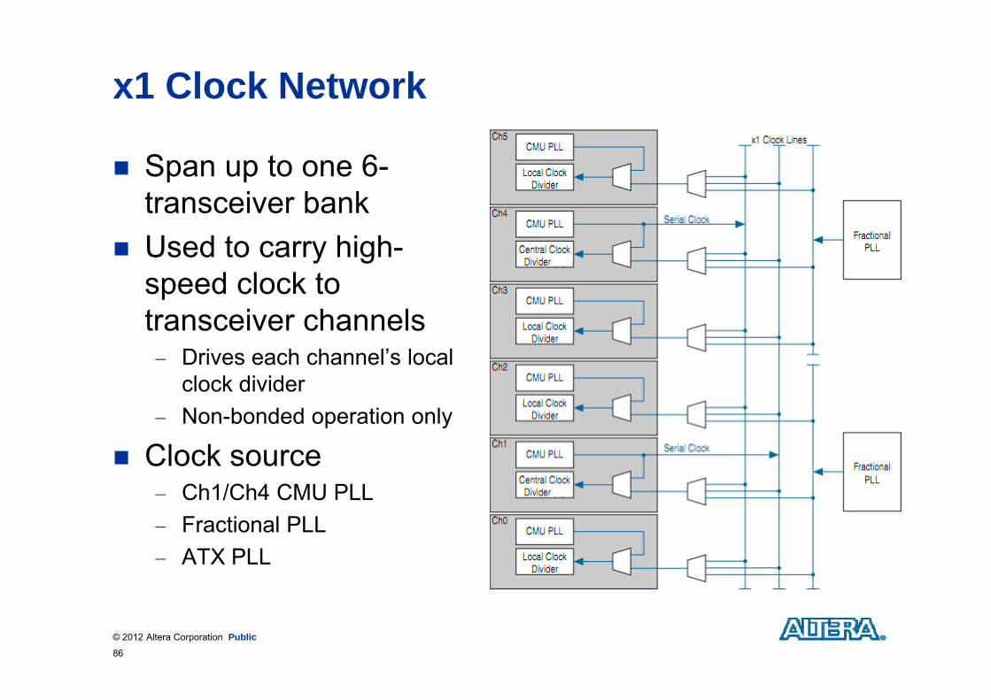
x1 Clock Network
Span up to one 6-i b ktransceiver bank
Used to carry high-speed clock to transceiver channels
D i h h l’ l l Drives each channel’s local clock divider
Non-bonded operation only
Clock source Ch1/Ch4 CMU PLL Fractional PLL ATX PLL
© 2012 Altera Corporation Public86

x6 Clock Network
Span up to one 6-t i b ktransceiver bank
Used to carry both high-speed serial and lowspeed serial and low-speed parallel clocks to channels within a 6-channels within a 6transceiver bank Bonded operation only
Clock source Central clock divider
© 2012 Altera Corporation Public87

xN Clock Network
Span the entire side of the d idevice
Used to carry both high-speed serial and low speedspeed serial and low-speed parallel clocks from x6 line to other transceiver banksother transceiver banks Bonded operations only
Clock source x6 clock network (from central clock
divider)
© 2012 Altera Corporation Public88

Internal Clocking: PLL Feedback Compensation P th B diPath Bonding
For bonding channels beyond a transceiver bankbeyond a transceiver bank with the controlled skew
Removes divider uncertainty by aligning parallel clk with refclk
Refclk restrictionRefclk restriction refclk frequency has to be
the same as tx_clkout fPLL can be used to match
refclk and parallel clock
© 2012 Altera Corporation Public

FPGA Fabric-Transceiver Interface Clocking
Quartus selectedTransmitter PCS Quartus selected option is best for: Bonded
TX FIFO
User selected
TX Data
tx coreclk
configurations User selected Parallel ClockQuartus selected
tx_clkout
tx_coreclk
option is best for: Saving FPGA
fabric clock
FPGA Fabric
RX Data
Receiver PCS
fabric clock resources for multiple identical
RX FIFO
User selectedrx_coreclk p
channelsParallel Clock(recovered by CDR)
Quartus selectedtx_clkout/rx_clkout
© 2012 Altera Corporation Public

T i R fi tiTransceiver Reconfiguration
© 2012 Altera Corporation—Public

Introduction
What is transceiver reconfiguration?
Reconfiguration of single or multiple transceiver channel settings during device operation
Reconfiguration ofg Physical media attachment (PMA) settings Physical coding sublayer (PCS) settings Transceiver Clocking (PLL settings)
Run time modification does not interrupt operation of adjacent transceiver channel(s)
© 2012 Altera Corporation Public92

Transceiver Reconfiguration Uses
Adjust transmitter/receiver buffer settings while bringing up link to fine-tune signal integrity Increases flexibility in board/system design
Increase/decrease data rate due to downstream/upstream device
Support newer, changing serial protocols Add design flexibility by supporting multiple Add design flexibility by supporting multiple
protocols with same hardware
© 2012 Altera Corporation Public93
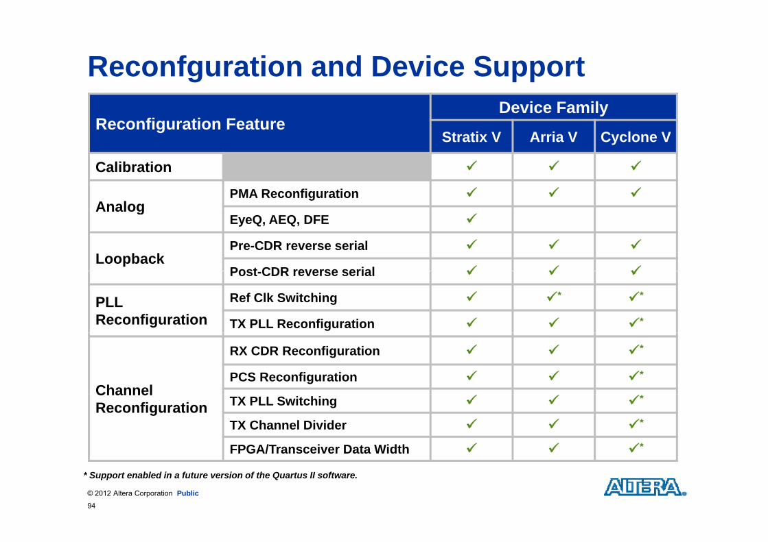
Reconfguration and Device Support
Reconfiguration FeatureDevice Family
Stratix V Arria V Cyclone V
Calibration
AnalogPMA Reconfiguration
AnalogEyeQ, AEQ, DFE
LoopbackPre-CDR reverse serial
Post CDR reverse serial Post-CDR reverse serial
PLLReconfiguration
Ref Clk Switching * *
TX PLL Reconfiguration *
Channel
RX CDR Reconfiguration *
PCS Reconfiguration *
Channel Reconfiguration TX PLL Switching *
TX Channel Divider *
FPGA/Transceiver Data Width *
© 2012 Altera Corporation Public94
* Support enabled in a future version of the Quartus II software.

Transceiver Reconfiguration Controller
Provides simple way to change transceiver tti d i llsettings dynamically
All types of reconfiguration require using controller Users must design custom hardware or software to interact withUsers must design custom hardware or software to interact with
controller based supported reconfiguration types
Uses general FPGA resources (soft IP) Connects to transceiver megafunctions/IP cores
using dedicated interface Some PHY IP blocks implemented with embedded controller core
Required in all PHY IP core designs, even if no i t ti f h i t i ttiintention of changing transceiver settings
© 2012 Altera Corporation Public95

Reconfiguration Modes
Register-basedReconfiguration initiated by read and write operations to controller Reconfiguration initiated by read and write operations to controller registers to reconfigure individual transceiver settings
Controller translates operations to specific transceiver registers Streamer based (MIF Mode) Streamer-based (MIF Mode)
Transceiver configuration data stored in ROM/RAM using a memory initialization file (MIF)Reconfiguration initiated by read and write operations to controller Reconfiguration initiated by read and write operations to controller registers
Upon initialization, controller steams MIF configuration data into transceiver registers to update transceiver settings all in one stepg p g p
Streamer-based (Direct Write Mode) Reconfiguration initiated by read and write operations to controller
registersregisters the user individually writes MIF words into individual transceiver
registers
© 2012 Altera Corporation Public96

Reconfiguration Features vs. Modes
Feature Register-Based Streamer-BasedgPMA
Loopback
EyeQ
AEQ
DFE DFE
ATX Tuning (Calibration)
Reference Clock Switch
PLL Reconfiguration
Channel Reconfiguration
© 2012 Altera Corporation Public97

Reconfiguration Diagram
© 2012 Altera Corporation Public98

Reconfiguration Controller Interfaces
FPGA Core Controller
Dynamic Reconfiguration Controller
↔ Controller
↔ Transceiver
Dynamic Reconfiguration Controller
mgmt_clk_clkmgmt_rst_resetreconfig mgmt addressreconfig_mgmt_addressreconfig_mgmt_writedatareconfig_mgmt_readdatareconfig_mgmt_writereconfig_mgmt_read
reconfig_to_xcvrreconfig_from_xcvr
reconfig_busy
Reconfiguration Management
Avalon-MM SlaveTransceiver Reconfiguration
reconfig_mgmt_waitrequest
reconfig_mif_addressreconfig_mif_read
fi if dd tMIF Reconfiguration
reconfig_mif_readdatareconfig_mif_waitrequest
Avalon-MM Master
© 2012 Altera Corporation Public99

Reconfiguration Management Interface
Interfaces between reconfiguration control logic and controllercontroller User logic employs read and write transfers using Avalon-MM master to setup,
start and monitor reconfiguration Example Avalon-MM masters: embedded processor state machine JTAGExample Avalon MM masters: embedded processor, state machine, JTAG
Avalon Master component
Interfacesmgmt clk clk mgmt_clk_clk Provides a clock for the reconfiguration interface Supported frequency range: 100 – 125 MHz
mgmt rst reset mgmt_rst_reset Resets the controller
reconfig_mgmt_* Avalon-MM slave interface made up of 7-bit address, 32-bit data and
read/write enable signals
© 2012 Altera Corporation Public100

MIF Reconfiguration Interface
Avalon-MM master interface between controller and MIF storage locationstorage location Controller accesses MIF data based on requests received through its slave
interface
Interface Interface reconfig_mif_*
Master interface made up of 32-bit address, 16-bit data, read enable and it t i lwaitrequest signals
© 2012 Altera Corporation Public101

Transceiver Reconfiguration Interface
Dedicated interface between controller and transceiver IP core Controller reads values from and writes values to transceiver registers based onController reads values from and writes values to transceiver registers based on
requests received through its slave interface
Each transceiver instance has 1 reconfiguration interface per each duplex transceiver channel and per each TX PLLeach duplex transceiver channel and per each TX PLL
Signals reconfig_to_xcvr[(n*70)-1..0]
O t t i l f t ll t t i IP i t ( ) Output signal from controller to transceiver IP core instance(s) n = number of reconfiguration interfaces
reconfig_from_xcvr[(n*46)-1..0] Input signal to controller from transceiver IP core instance(s) Input signal to controller from transceiver IP core instance(s) n = number of reconfiguration interfaces
reconfig_busy Output signal that indicates when a reconfiguration operation is in progress Output signal that indicates when a reconfiguration operation is in progress Similar to the busy bits (bit 8) in the control and status registers
© 2012 Altera Corporation Public102

Reconfiguration Controller Address MapReconfiguration Feature
7-bit Address Range
Start End
PMA 0x08 0x0C
EyeQ 0x10 0x14
DFE 0 18 0 1CDFE 0x18 0x1C
AEQ 0x28 0x2C
ATX PLL Calibration 0x30 0x34
Streamer-Based/Direct Write-Based 0x38 0x3C
PLL Reconfiguration 0x40 0x44g
Features assigned defined address ranges in reconfiguration controller’s Avalon-MM address space User logic sets up/activates a feature in controller by accessing registers in feature’s address range Within controller, features have own internal address spaces for accessing specific feature settings User logic programs feature setting by writing a value into an offset register (e.g. PMA=0x0B,
EyeQ=0x13) . The offset value corresponds to the internal address of that feature setting. Reconfiguration controller uses offset value to access the correct internal address for that feature
© 2012 Altera Corporation Public103
* Any undefined register addresses are reserved.
Reconfiguration controller uses offset value to access the correct internal address for that feature

Controller Offset Example
Transceiver Reconfiguration Controllerg
Internal PMA Address SpaceController Avalon-MM Address Space
Offset (Address) Data Register Name
0x0 VOD0x28
Address Data Register Name
0x08 PMA LogicalChannel Address0x02
Controller Logic
0x01 Pre-emphasis Pre-Tap
0x02 Pre-emphasis 1st
Post-Tap
Pre emphasis 2nd
Channel Address
0x09 PMA PhysicalChannel Address
0x0A PMA Control/Status0x010x01
0x03 Pre-emphasis 2nd
Post-Tap
0x10 Equalization DC Gain
●●● ●●●
0x3
0x0B PMA Offset
0x0C PMA Offset Data
●●● ●●●
0x0
0x28
0x10
0x3
© 2012 Altera Corporation Public104

Logical Channel Numbers
Reference numbers used to represent actual physical transceiver channels and TX PLLsphysical transceiver channels and TX PLLs
Used during reconfiguration to target specific channels or PLLschannels or PLLs Controller translates read/write operations to logical channel
numbers to their corresponding physical channels
Assigned to physical transceivers automatically based on
Number of channels and TX PLLs in transceiver IP cores Number of channels and TX PLLs in transceiver IP cores Order in which the reconfiguration interfaces are physically
connected to controllerVie the assignment res lts in the Transcei er Reconfig ration View the assignment results in the Transceiver Reconfiguration Report (Compilation Report → Fitter → GXB Reports)
© 2012 Altera Corporation Public105

Basic Register-Based Write Operation1. Read feature control and status register to
determine busy bit is 0y2. Write target logical channel number to feature’s
logical_channel_address register3. Write the internal address (offset) value to feature’s
offset register4. Write the target value for the feature setting into the
feature data registerW it f t ’ t l d t t i t it bit5. Write feature’s control and status register write bit with 1
6 Transceiver is programmed when busy bit is 06. Transceiver is programmed when busy bit is 0 again
© 2012 Altera Corporation Public106

Basic Register-Based Read Operation1. Read feature control and status register to
determine busy bit is 0determine busy bit is 02. Write target logical channel number to feature’s
logical_channel_address registerg _ _ g3. Write the internal address (offset) value to feature’s
offset register4. Write feature’s control and status register read bit
with 15. Read operation is complete when busy bit is 0
againR d th f t ’ d t i t f th l f th6. Read the feature’s data register for the value of the feature setting returned by the read operation
© 2012 Altera Corporation Public107

Reconfiguration Modes: Streamer Based
Two available modes: Mode 0: MIF Streaming Mode 1: Direct Writes
Reconfiguration data is contained in a MIF Supports:
PLL counters Reference clocks Local clock dividers
… basically you get just about everything not available through register based
© 2012 Altera Corporation Public108
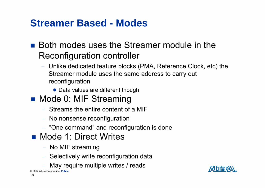
Streamer Based - Modes
Both modes uses the Streamer module in the Reconfiguration controller Unlike dedicated feature blocks (PMA, Reference Clock, etc) the
Streamer module uses the same address to carry outStreamer module uses the same address to carry out reconfiguration Data values are different though
Mode 0: MIF Streaming Streams the entire content of a MIF No nonsense reconfiguration “One command” and reconfiguration is done
Mode 1: Direct Writes Mode 1: Direct Writes No MIF streaming Selectively write reconfiguration data
© 2012 Altera Corporation Public109
Selectively write reconfiguration data May require multiple writes / reads

Modes 0 MIF Streamer - Flow
6. Write Start MIF Stream (1’b1) to the “feature”offset register at 0x3B
1. Write <Channel or PLL logical number> to the logical channel register at 0x38
g
7. Write 1’b1 to the data register at 0x3C
8 W it 1’b1 t bit[0] f th t l d t t
2. Write MIF mode 0 (2’b00) to the control and status register at 0x3A
3. Write the MIF base address (1’b0) value to the 8. Write 1’b1 to bit[0] of the control and statusregister at 0x3A
9. Read the “busy” bit of control and status
( )“feature” offset register at 0x3B
4. Write <base address of the MIF> to the dataregister at 0x3C
register5. Write 1’b1 to bit[0] of the control and statusregister at 0x3A
g
Steps similar to register based reconfiguration Steps { 3 , 4 , 5 } and { 6 , 7 , 8 } use the same sequence just
writing different values
© 2012 Altera Corporation Public110

Modes 1 Direct Writes - Flow
1. Write <Channel or PLL logical number>to the logical channel register at 0x38
offset value[10:0]length [15:11]to the logical channel register at 0x38
2. Write MIF mode 1 (2’b01) to the control and status register at 0x3A
0001100000000000 ; -- PMA - TX 0010000000100000 ;0000110000000000 ; offset data
3. Write the <offset value> value to the “feature” offset register at 0x3B
4 W it ff t d t t th d t i t t
0000110000000000 ;0000000000100000 ;
offset data
4. Write <offset data> to the data register at 0x3C
5. Write 1’b1 to bit[0] of the control and The length field
determines the numberstatus register at 0x3A determines the number of loops
Must increment theAll offset data
Must increment the offset value by 0x1 after each loop
written?
© 2012 Altera Corporation Public111
9. Read the “busy” bit of control and status register
each loop

Enabling Transceiver Reconfiguration
User must configure1. IP megafunction containing embedded transceivers2. Transceiver Reconfiguration Controller megafunctiong g
Purpose Enable reconfiguration options Ensure controller has the correct number of
reconfiguration interfaces
© 2012 Altera Corporation Public112

8 total reconfiguration interfaces needed
Interfaces 0-3 are assigned
© 2012 Altera Corporation Public113
gto the transceiver channels
Interfaces 4 - 7 are assigned to the TX PLLs

16 total reconfiguration16 total reconfiguration interfaces needed (sum from each transceiver IP block to be connected
Specifies how reconfiguration interfaces should be grouped; “8,8” means this controller ismeans this controller is connected to 2 transceiver IP blocks, each with 8 reconfiguration interfaces
Enable reconfiguration modes to be supported by controller
© 2012 Altera Corporation Public114

Reconfiguration Interface Merging
All transceiver channels and TX PLLs generate an interface on the controller and transceiver megafunction
Quartus II software automatically merges interfaces as transceiver functionality is mergedy g e.g. Shared TX PLLs
Starting with separate interfaces gives Fitter g p gmore flexibility in placement as it can merge any interfaces as needed
© 2012 Altera Corporation Public115

Controller Design Example Scenarios
1. Connecting to 1 PHY IP core with bonded channels
2. Connecting to 1 PHY IP core with non-bonded gchannels
3 Connect to 2 PHY IP cores3. Connect to 2 PHY IP cores
© 2012 Altera Corporation Public116

One PHY IP Core with Bonded Channels
One 4 channel Custom PHY IP core instance One 4-channel Custom PHY IP core instance One transceiver reconfiguration controller
© 2012 Altera Corporation Public117
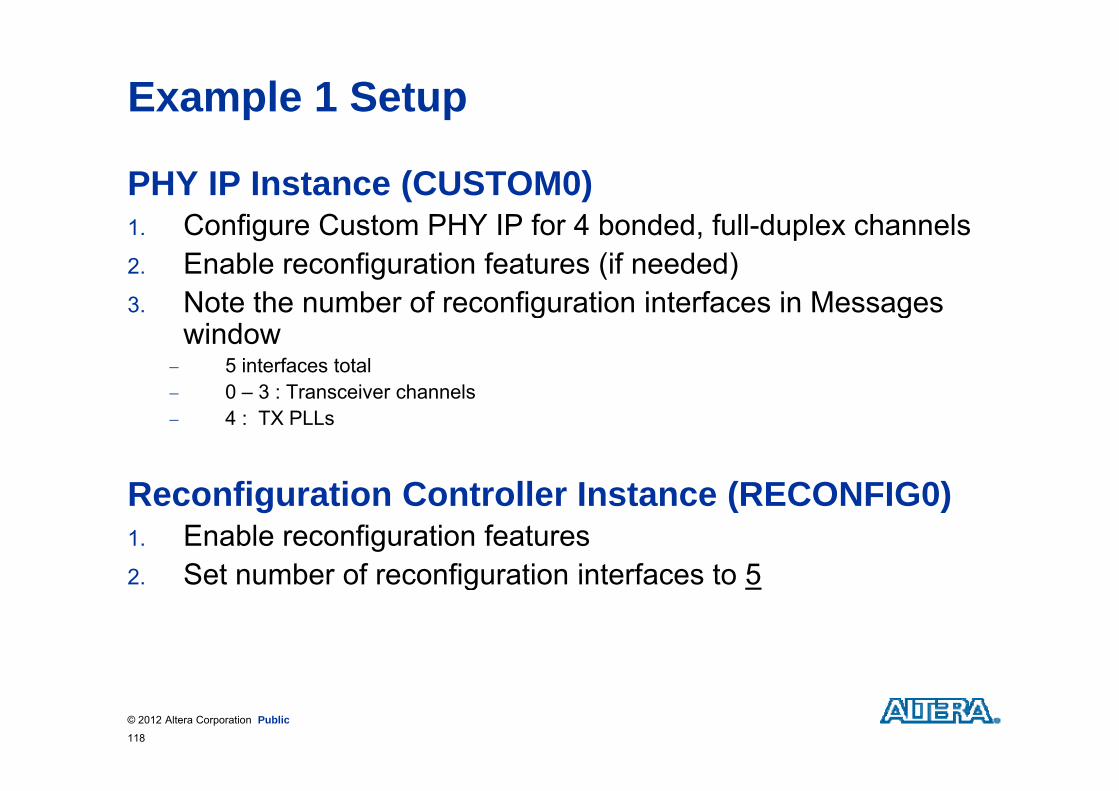
Example 1 Setup
PHY IP Instance (CUSTOM0)C fi C t PHY IP f 4 b d d f ll d l h l1. Configure Custom PHY IP for 4 bonded, full-duplex channels
2. Enable reconfiguration features (if needed)3 Note the number of reconfiguration interfaces in Messages3. Note the number of reconfiguration interfaces in Messages
window 5 interfaces total 0 – 3 : Transceiver channels0 3 : Transceiver channels 4 : TX PLLs
R fi ti C t ll I t (RECONFIG0)Reconfiguration Controller Instance (RECONFIG0)1. Enable reconfiguration features2 Set number of reconfiguration interfaces to 52. Set number of reconfiguration interfaces to 5
© 2012 Altera Corporation Public118

Example 1 Block Diagram w/ Connections
CUSTOM0reconfig busy
reconfig_to_xcvr[349:0]mgmt_clk
mgmt reset
reconfig_mgmt_*
RECONFIG0 (4 Bonded Channels)
reconfig_busyg _
reconfig_from_xcvr[229:0]
RECONFIG0
N b f i t f 5reconfig_from_xcvr[229:0]
Number of interfaces = 5
CUSTOM0.reconfig_from_xcvr[229:0] RECONFIG0.reconfig_from_xcvr[229:0]
RECONFIG0.reconfig_to_xcvr[349:0] CUSTOM0.reconfig_to_xcvr[349:0]
© 2012 Altera Corporation Public119

Transceiver Reconfiguration Report
Logical channel number assignments
Logical Channel Number Channel Name
0 Channel 01 Ch l 11 Channel 12 Channel 23 Channel 3
© 2012 Altera Corporation Public120
4 TX (CMU) PLL

One PHY IP Core with Non-Bonded Channels
One 4 channel Custom PHY IP core instance One 4-channel Custom PHY IP core instance One transceiver reconfiguration controller
© 2012 Altera Corporation Public121

Example 2 Setup
PHY IP Instance (CUSTOM0)1 Configure Custom PHY IP for 4 non bonded full duplex1. Configure Custom PHY IP for 4 non-bonded, full-duplex
channels2. Enable reconfiguration features (if needed)
N t th b f fi ti i t f i M3. Note the number of reconfiguration interfaces in Messages window
8 interfaces total0 3 : Transceiver channels 0 – 3 : Transceiver channels
4 – 7 : TX PLLs
Reconfiguration Controller Instance (RECONFIG0)Reconfiguration Controller Instance (RECONFIG0)1. Configure transceiver reconfiguration controller2. Enable reconfiguration featuresg3. Set number of reconfiguration interfaces to 8
© 2012 Altera Corporation Public122

Example 2 Block Diagram w/ Connections
CUSTOM0(4 Nonreconfig busy
reconfig_to_xcvr[559:0]mgmt_clk
mgmt reset
reconfig_mgmt_*
RECONFIG0 (4 Non-Bonded
Channels)
reconfig_busyg _
reconfig_from_xcvr[367:0]
RECONFIG0
Number of interfaces = 8reconfig_from_xcvr[367:0]
Number of interfaces = 8
CUSTOM0.reconfig_from_xcvr[367:0] RECONFIG0.reconfig_from_xcvr[367:0]
RECONFIG0.reconfig_to_xcvr[559:0] CUSTOM0.reconfig_to_xcvr[559:0]
© 2012 Altera Corporation Public123

Transceiver Reconfiguration Report
Logical Channel Number Channel Name
0 Channel 0
1 Channel 1
2 Channel 2
3 Channel 3
© 2012 Altera Corporation Public124
4, 5, 6, 7 TX (CMU) PLL (Channels 0 – 3)

Two PHY IP Cores with Non-Bonded Cores
Two 4 channel Custom PHY IP core instances Two 4-channel Custom PHY IP core instances One transceiver reconfiguration controller
© 2012 Altera Corporation Public125

Example 3 Setup4-Channel Instance (CUSTOM0)1. Configure Custom PHY IP for 4 non-bonded, full-duplex channels2 Enable reconfiguration features (if needed)2. Enable reconfiguration features (if needed)3. Note the number of reconfiguration interfaces in Messages window
8 interfaces total 0 – 3 : Transceiver channels 4 – 7 : TX PLLs
4-Channel Instance (CUSTOM1)1. Configure Custom PHY IP for 4 non-bonded, full-duplex channels
f f ( f )2. Enable reconfiguration features (if needed)3. Note the number of reconfiguration interfaces in Messages window
8 interfaces total 0 – 3 : Transceiver channels
4 7 TX PLL 4 – 7 : TX PLLs
Reconfiguration Controller Instance (RECONFIG0)1 Configure transceiver reconfiguration controller1. Configure transceiver reconfiguration controller2. Enable reconfiguration features3. Set number of reconfiguration interfaces to 164. Set the grouping to 8,8
© 2012 Altera Corporation Public
g p g
126

Example 3 Block Diagram w/ConnectionsCUSTOM0
(4 Non-Bonded
reconfig_to_xcvr
Bonded Channels) reconfig_from_xcvr
ch8_15_to_xcvr
CUSTOM1
ch0_7_to_xcvrmgmt_clk
mgmt_reset
reconfig_mgmt_*
RECONFIG0reconfig_busy
CUSTOM1(4 Non-Bonded
Channels) reconfig from xcvrch8_15_from_xcvr
RECONFIG0
Number of Interfaces = 16Interface Grouping = 8 8
reconfig_to_xcvrch0_7_from_xcvr
Channels) reconfig_from_xcvrInterface Grouping = 8,8
CUSTOM0 reconfig from xcvr RECONFIG0 ch0 7 from xcvrCUSTOM0.reconfig_from_xcvr RECONFIG0.ch0_7_from_xcvr
CUSTOM1.reconfig_from_xcvr RECONFIG0.ch8_15_from_xcvr
RECONFIG0.ch0_7_to_xcvr CUSTOM0.reconfig_to_xcvr
RECONFIG0.ch8 15 to xcvr CUSTOM1.reconfig to xcvr
© 2012 Altera Corporation Public127
CO G0 c 8_ 5_to_ c CUS O eco g_to_ c

Example 3 Logical Channel Number Assignments*
Logical Channel Number Channel Name
0 CUSTOM0 Channel 01 CUSTOM0 Ch l 11 CUSTOM0 Channel 12 CUSTOM0 Channel 23 CUSTOM0 Channel 38 CUSTOM1 Channel09 CUSTOM1 Channel110 CUSTOM1 Channel210 CUSTOM1 Channel211 CUSTOM1 Channel3
4, 5, 6, 7 CUSTOM0 CMU PLL12,13,14,15 CUSTOM1 CMU PLL
© 2012 Altera Corporation Public128
* One possible solution
Calibration
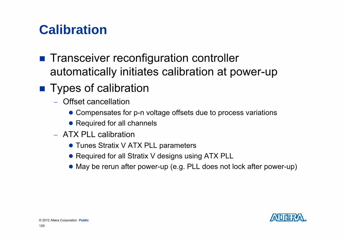
Transceiver reconfiguration controller automatically initiates calibration at power-up
Types of calibrationyp Offset cancellation
Compensates for p-n voltage offsets due to process variationsR i d f ll h l Required for all channels
ATX PLL calibration Tunes Stratix V ATX PLL parametersp Required for all Stratix V designs using ATX PLL May be rerun after power-up (e.g. PLL does not lock after power-up)
© 2012 Altera Corporation Public129

Megafunction Settings for Calibration
Offset cancellation automatically enabled in controller megafunction
Other calibration types/options must be enabledyp pTransceiver
Reconfiguration Controller
© 2012 Altera Corporation Public130

Performing Calibration
1. Upon power-up, transceiver reconfiguration controller i iti t lib tiinitiates calibration
2. Embedded reset controller triggers reset when completeM it fi b t t fl b i t t3. Monitor reconfig_busy output flag or busy register to determine when controller is done
4 Monitor tx ready and rx ready signals to learn when4. Monitor tx_ready and rx_ready signals to learn when channels are ready to send/receive data
© 2012 Altera Corporation Public131

PMA Reconfiguration
Selects from thousands of transmit and receive PMA analog settings dynamically
Use to Improve signal integrity during in-system tests and debuggingp g g y g y gg g
Fine tune transmit/receive buffers according to specific board/system conditions
Manually adjust settings to achieve target BER in FPGA or Manually adjust settings to achieve target BER in FPGA or upstream device
© 2012 Altera Corporation Public132

Configurable PMA Settings
Output differential voltage (VOD) Pre-emphasis support Equalization Equalization Equalizer DC gain
© 2012 Altera Corporation Public133

Enables PMA reconfiguration
© 2012 Altera Corporation Public

Memory Initialization File
Used during reconfiguration to store settings for a single t i h l d/ PLLtransceiver channel and/or PLL Stores a single transceiver state To support multiple transceiver configurations, you must generate and store
multiple MIFs
Generated automatically by Quartus II Assembler based on transceiver PHY IP core settingson transceiver PHY IP core settings
For design implementation, configure transceiver IP core for each set of reconfiguration options and recompilefor each set of reconfiguration options and recompile Each recompilation creates a reconfiguration MIF For faster compile times, consider creating a simplified reference or
t l t d itemplate design
Reconfigure channels by writing new MIF into channel
© 2012 Altera Corporation Public135

Using MIFs
Each MIF files has the settings for single or full duplex channelchannel Each MIF file is made up of 16-bit records (words)
Number of words determined by target device and target channel(s)N li it ti th b f MIF i l t d i i l d i No limitation on the number of MIFs implemented in a single design
Single MIF can be used for reconfiguring multiple channels
MIFs can be stored in embedded RAM or in off-chip pmemory
Reconfiguration controller automatically accesses MIF d th h MIF fi ti A l MM trecords through MIF reconfiguration Avalon-MM master
interface Reconfiguration controller writes MIF records into actual Reconfiguration controller writes MIF records into actual
transceiver channel(s)
© 2012 Altera Corporation Public136

MIF ExampleFPGA
UserControlLogic R fi ti
Transceiver Channel 0Logic Reconfiguration
ControllerTransceiver Ch l 1Channel 1
OC_48 MIFMIF
GIGEMIF
CustomMIF
© 2012 Altera Corporation Public137
Note: MIFs can be stored in single memory or separate memory spaces

Locating Generated MIFs
reconfig_mif subdirectory created in project directory
Separate MIF created for each transceiver IP pinstance and each TX PLLs referenced in those instances
Default filenames based on the transceiver IP instance namesinstance names User can rename MIF
© 2012 Altera Corporation Public138

Input Reference Clocks
PHY IP clock sources for TX PLLs and RX CDRsT i f ti t t 5 diff t i t Transceiver megafunction supports up to 5 different input reference clocks when channel and PLL reconfiguration enabled
Changing input reference clocks changes input clock frequency to PLLs and CRUs Allows support for wider variety of data rates vs. changing PLL settings
alone
© 2012 Altera Corporation Public139

More Details on Channel & PLL Reconfiguration
Online documentation Stratix V Device Handbook, Volume 3, Chapter 6: Dynamic
Reconfiguration in Stratix V DevicesArria V Device Handbook Volume 3 Chapter 7: Dynamic Arria V Device Handbook, Volume 3, Chapter 7: Dynamic Reconfiguration in Arria V Devices
Altera Transceiver PHY IP Core User Guide
© 2012 Altera Corporation Public148

Connection Considerations
Stratix V supports one Avalon interface per triplet Two AVMM per six-pack
AVMM interface needs to be taken into account when planning the Reconfiguration Controller connections
AVMMCh l 3Channel 4Channel 5
AVMM
Channel 0Channel 1Channel 2
Channel 3
Channel 0
© 2012 Altera Corporation Public149
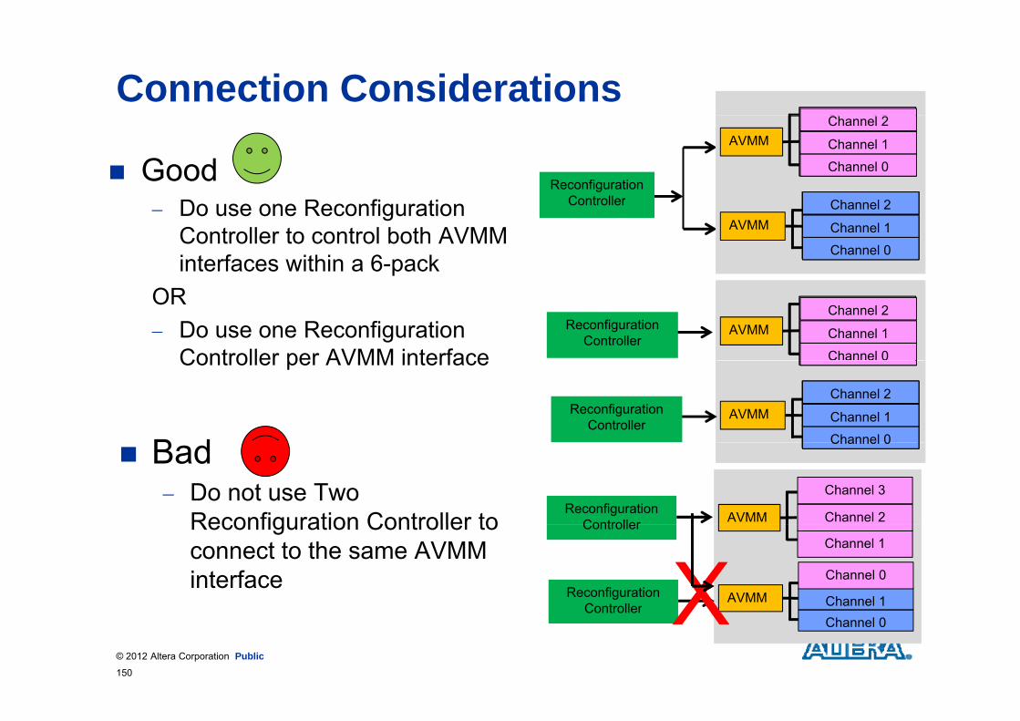
Connection ConsiderationsCh lCh l
Good ReconfigurationC t ll
AVMM
Channel 3
Channel 4
Channel 5
Channel 3
Channel 4
Channel 5
Channel 0
Channel 1
Channel 2
Do use one Reconfiguration Controller to control both AVMM interfaces within a 6-pack
Controller
AVMM
Channel 0
Channel 1
Channel 2
Channel 0
Channel 1
Channel 2
Channel 0
Channel 1
Channel 2
OR Do use one Reconfiguration
Controller per AVMM interfaceAVMM
Channel 3
Channel 4
Channel 5Reconfiguration
ControllerChannel 3
Channel 4
Channel 5
Channel 0
Channel 1
Channel 2
Controller per AVMM interface
B dAVMM
Channel 0
Channel 1
Channel 2Reconfiguration
ControllerChannel 0
Channel 1
Channel 2
Channel 0
Channel 1
Channel 2
Bad Do not use Two
Reconfiguration Controller to
Channel 0Channel 0Channel 0
AVMM Channel 2
Channel 3Reconfiguration
ControllerReconfiguration Controller to connect to the same AVMM interface
AVMM Channel 1
Channel 0
Channel 1Controller
ReconfigurationController X
© 2012 Altera Corporation Public150
Channel 0Controller X

DPRIO Demo Design using MIF Streamer Mode 0 V12.0.0For the Stratix V GX SI BoardDynamically reconfigure between 2 dataratesPeter SchepersPeter SchepersStaff Technology Specialist FAE High Speed InterfacesJune 28th , 2012
© 2012 Altera Corporation—Public

Blockdiagram
© 2012 Altera Corporation Public152

Transceiver Configuration 1st datarate (General Tab)
© 2012 Altera Corporation Public153

Transceiver Configuration 1st Datarate (Reconfiguration Tab)
“Allow PLL Reconfiguration” must be checked Allow PLL Reconfiguration must be checked As 2 input referenceclocks will be used the number of input clocks
should be set to ‘2’. For the first datarate the referenceclock with index 0 will be used for
b th th T th R
© 2012 Altera Corporation Public154
both the Tx as the Rx

Transceiver Configuration 2nd datarate (General Tab)
The 2nd datarate is 8.5 Gbps from a 425 Mhz reference clock
© 2012 Altera Corporation Public155

Transceiver Configuration 2nd Datarate (Reconfiguration Tab)
Note that the TX PLL will be reconfigured in this example so there is Note that the TX PLL will be reconfigured in this example so there is only one TX PLL Logical Index
For the first datarate the referenceclock with index 1 will be used for both the Tx as the Rx (Input clock source)
© 2012 Altera Corporation Public156
both the Tx as the Rx (Input clock source)

Reconfiguration Controller
“Enable channel/PLL reconfiguration support block” must be checked (This will enable the reconfig_mif interface in the reconfiguration
t ll )
© 2012 Altera Corporation Public157
controller).

Reconfiguration Hardware Controller (Blockdiagram)
© 2012 Altera Corporation Public158

Reconfiguration Hardware Controller (Description) The Reconfiguration_Hardware_Controller Instance is a module which
controls the reconfiguration controller (xcvr_reconfig) module through a HW statemachine (see further).( )
Since there are 2 datarates being used there are in total 4 MIF files required : 2 for each datarate : one for the Channel (Tx/Rx) and one for the PLL.
These MIF files are automatically generated during the compilation These MIF files are automatically generated during the compilation. In order to generate the MIF files for the 2nd datarate one needs to instantiate
the 2nd datarate PHY instead of the 1st one and recompile the design (alternatively one can also use a dummy design which only instantiates the(alternatively one can also use a dummy design which only instantiates the PHY and the reconfiguration controller using the same pinouts as the final design).
The MIF files are stored in the ROM as indicated in the blockdiagram and a The MIF files are stored in the ROM as indicated in the blockdiagram and a small arbiter (av_master) controls the accesses to the ROM’s and generates the reconfig_mif_waitrequest signal accordingly.
There is a MUX after the ROM’s which will select the proper mif readdata to There is a MUX after the ROM s which will select the proper mif_readdata to feed it back to the reconfiguration controller.
© 2012 Altera Corporation Public159

Phy Management Interface. The Stratix V PHY instance has a Phy Management Interface which is used
to control the resets and the serial loopback. This PHY Management Interface is an Avalon MM Interface. This design is using a QSYS system which transparently maps an Avalon
MM interface to the PHY Management Interface of the PHY. The component created for this in QSYS is called “phy_mgmt” and the
phy_mgmt_hw.tcl file included in the project describes it’s implementation. You can verify it’s content by editing the phy_mgmt component.
© 2012 Altera Corporation Public160

Reconfig Management Interface. The transceiver reconfiguration controller also has an Avalon MM Interface
which is used to control the PMA settings of the transceivers the reconfiguration controller is connected toreconfiguration controller is connected to.
Similar to the Phy Management Interface this design is also using the QSYS system which transparently maps another Avalon MM interface to the Reconfiguration Management Interface of the reconfiguration controller.Reconfiguration Management Interface of the reconfiguration controller.
The component created for this in QSYS is called “reconfig_mgmt” and the reconfig_mgmt_hw.tcl file included in the project describes it’s implementation. p
You can verify it’s content by editing the reconfig_mgmt component.
© 2012 Altera Corporation Public161

Nios 2 Output in Nios II SDK ShellNios II SDK Shell
© 2012 Altera Corporation Public162

Signal Conditioning and Best PracticesSignal Conditioning and Best Practices for Link TuningP t S hPeter Schepers
© 2012 Altera Corporation—Public

Signal Integrity Challenge at 10 Gbps and b dbeyond Shrinking Margins
1 UI 80 @ 12 Gb ! 1 UI = 80 ps @ 12.5 Gbps ! 1 UI = 35 ps @ 28 Gbps !!
BER targets more stringent BER targets more stringent Interlaken, CEI-11G, SFI-5.2, SFI-S : 1E-15
Tighter skew requirementsg q SFI-S requires skew of 5.5 UI at Tx
Need to drive backplanesSpecification Data Rate Reach BER10GBASE-KR 10.3125Gbps 1m (39”) + 2
connectors< 1E-12
connectorsCEI-11G-LR 11.1Gbps 1m (39”) + 2
connectors<1E-15
© 2012 Altera Corporation Public164
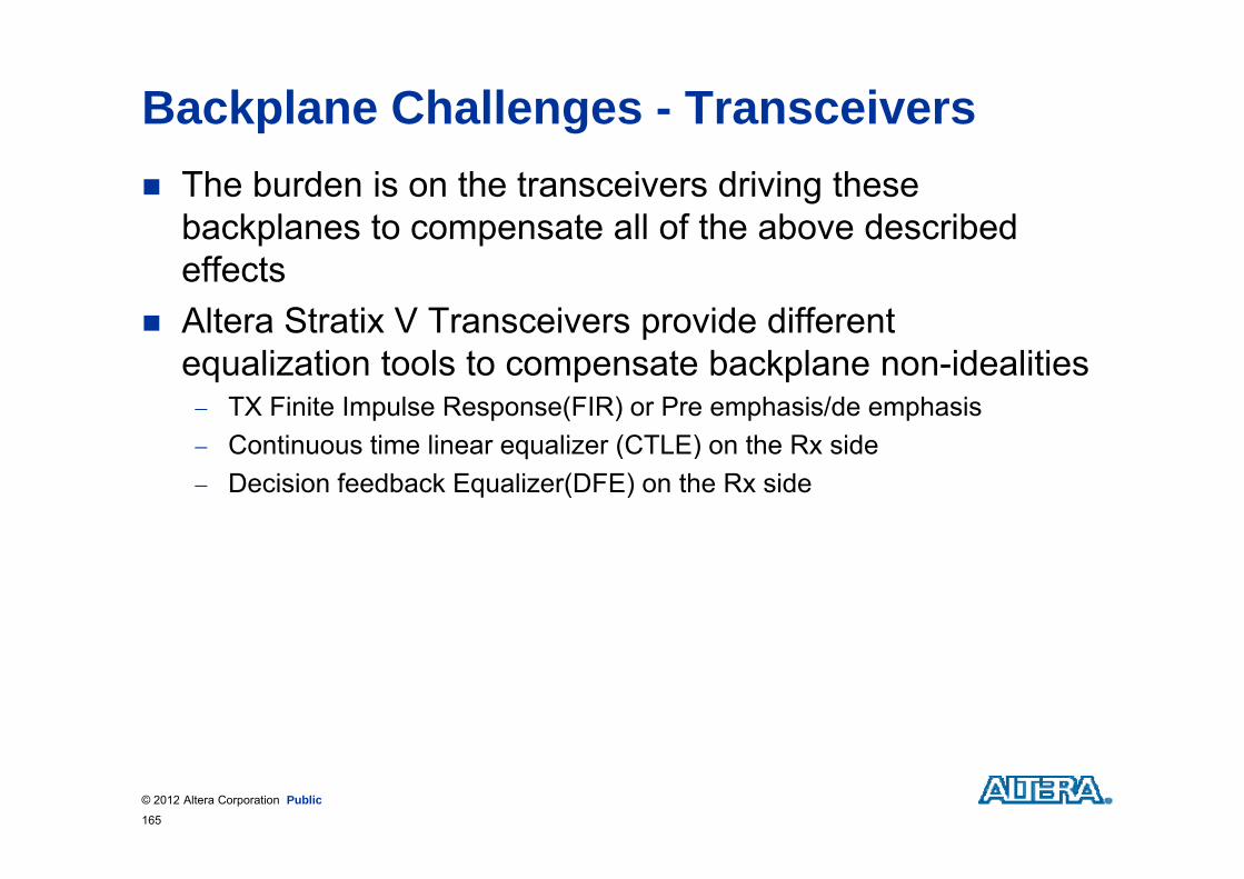
Backplane Challenges - Transceivers The burden is on the transceivers driving these
backplanes to compensate all of the above described p peffects
Altera Stratix V Transceivers provide different equalization tools to compensate backplane non-idealities TX Finite Impulse Response(FIR) or Pre emphasis/de emphasis
C ti ti li li (CTLE) th R id Continuous time linear equalizer (CTLE) on the Rx side Decision feedback Equalizer(DFE) on the Rx side
© 2012 Altera Corporation Public165

Physics for Electrical Channel LossElectrical loss function
0 2 4 6 8 10 12
10
-5
00 2 4 6 8 10 12
-20
-15
-10
s (d
B)
Skin
35
-30
-25
Loss Dielectric
-45
-40
-35Skin + dielectric
-50
Frequency (GHz)
© 2012 Altera Corporation Public166

Mechanisms for Equalization
0dB 0dB 0dB
Channel Equalizer =+ Flat overall response
f f f
Tx equalizer: pre-emphasis, de-emphasis
Rx equalizer: linear (CTLE or FFE) or adaptive (DFE)
Make the lossy channel a non-lossy channel
de emphasis or adaptive (DFE)
y yso the overall “effective channel” is an
“all-pass” function or has a flat response
© 2012 Altera Corporation Public167

Equalization Architecture Overview
Equalization
N li
Equalization
Linear Nonlinear
Continuous time (e.g., CTLE)
Discrete time (e.g.,FIR)
Decision feedback (DFE)
RxTx
© 2012 Altera Corporation Public168

Ideal Pulse (IP), Single Pulse Response (SPR), and DFE Tap Coefficients
Time-shifted IPMain cursor/tapp
Post-cursors/taps
Pre-cursors/tapsSPR
C1 C2 C3 C4C5
© 2012 Altera Corporation Public169

Transmitter (Tx) Buffer Altera Stratix V Transmit buffer drives pair of differential
signals through a pair of 50ohm impedance Tx offers programmable drive strength, pre emphasis and
common mode voltage for enhanced signaling
T
Main tap pre driver
Txp
Rterm
Post tap Pre driver
Tx Driver
Rterm
Vcm
Txn
© 2012 Altera Corporation Public170
Tx Buffer Structure

Tx Pre/de emphasis When signal travelling through a lossy (insertion loss)
back plane, the transition expands to adjacent intervals, creating Inter symbol interference(ISI)
Tx signal can be pre distorted(emphasis) so that after it goes through backplane, resulting signal is cleaner for Rx
In general, two ways of pre conditioning the signal Amplify high frequency contents Pre-emphasis Reduce low frequency contents De-emphasis
Ref: AN 602
© 2012 Altera Corporation Public171
Pulse response – pre conditioning

Tx Pre/de emphasis contd.. Altera Stratix V devices provide one pre-tap to address
pre cursor(before transition of bit) ISI and two post taps to compensate post cursor(after transition of bit) ISI This is accomplished by taking delayed (z-1 Tx(n-1)) version of
transmit data and adding its weighted value to the actual datatransmit data and adding its weighted value to the actual data
Ref: AN 602Tx Pre/de emphasis Effect of pre emphasis
© 2012 Altera Corporation Public172
Ref: AN 602

Tx 1st post tap effect 1st post tap is most effective tap
It emphasizes bit period immediately after transition and de emphasizes remaining bitbits
The emphasis part is not as significant as de emphasis part De emphasis reduces vod level and minimizing signal power
O l iti l it f fi t t t Only positive polarity for first post tap
Id l ff t f 1 t t t Measure of post tap effect
20log(B/A) in dB
Ideal effect of 1st post tap
© 2012 Altera Corporation Public173

Tx 1st post tap effect Stratix V 1st post tap effect in dB
Note that pre emphasis is not very significant until the setting of 15
© 2012 Altera Corporation Public174

Tx pre tap effect The pre tap de emphasizes bit before transition and
emphasizes remaining bits Negative polarity of pre tap does the opposite effect Stratix V Tx buffer has +/-15 pre tap values
Pre tap has range of -1db to 2dbPre tap has range of 1db to 2db
Ideal effect of pre tap
© 2012 Altera Corporation Public175
Ideal effect of pre tap

Tx 2nd post tap effect 2nd post tap de emphasizes first two bits after transition
and emphasizes remaining bits Negative polarity does the opposite effect Stratix V has +/-15 2nd post tap values
2nd post tap has less effect relatively it has range of 0 8db to 1 5db 2nd post tap has less effect relatively, it has range of 0.8db to 1.5db
© 2012 Altera Corporation Public176
Ideal effect of 2nd post tap

Receiver Equalization
Stratix V receivers feature the following two types of equalizers Continuous Time Linear Equalizer (CTLE) Decision Feedback Equalizer (DFE)
Continuous RX
Decision To Receiver Time Linear Equalizer(CTLE)
RX Buffer
Feedback Equalizer
(DFE)
CDR and EyeQ
Circuitry
Adaptive EQ
Manual(Dynamic Adaptive
Manual(DynamicEQ
(AEQ)(Dynamic Reconfig)
U
Adaptive (Dynamic Reconfig)
© 2012 Altera Corporation Public177
User Logic
BER/CRC Monitor

Rx Equalizer/CTLE The equalizer boosts high frequency components and compensates
backplane loss The goal of equalizer is able to fit/compensate different backplane
losses Based on analysis of different backplanes at 10.3Gbps, Stratix V 4 stageBased on analysis of different backplanes at 10.3Gbps, Stratix V 4 stage
Rx Equalizer is designed
© 2012 Altera Corporation Public178
Simple Equalization response 4 stage CTLE curves

Rx Equalizer/CTLE Rx Equalizer has programmable controls on
DC Gain boost up to 12dB and serves as variable Gain amplifier Slope adjustment up to 80db/dec with 4 stages High frequency gain adjustment up to 16db
With out enabling of any stages, there is still AC gain of ~5dB for g y g , gEqualizer
Bandwidth adjustment for 6.25Gbps and 12.5Gbps
Stratix V default DC gain is changed to 3dB Stratix V default DC gain is changed to 3dB
© 2012 Altera Corporation Public179
DC GAIN 0dB DC GAIN 3DB

Adaptive Equalization (AEQ) In order to tune CTLE to fit to many of different customer
backplanes and to avoid manual selection of ~240 settings on CTLE, Adaptive engine is required
Modes of AEQ Continuous adaptation
Continuously adjusting 4stage equalizer settings based on input data One time Adaptationp
Adapts 4 stage EQ settings and freezes those values. Low power consumption
Manual User picks one of 16 available AC settings and DC settings.
© 2012 Altera Corporation Public180

Adaptive Equalization (AEQ) Continuous Adaptation
The low frequency content and high frequency content of reference edge generator and equalizer are matched in a feed back mechanism Low frequency and high frequency content are extracted using low Low frequency and high frequency content are extracted using low
pass and high pass filters Adaptation done signal goes high after matching of signals
frequency contentfrequency content
ReferenceG4 Stage EQ Gen4 Stage EQ
Block diagram of AEQAdaptation mechanism
© 2012 Altera Corporation Public181
Low freq& High freq feedback

Decision feedback Equalization (DFE) DFE is non linear system of equalization DFE works by actively shifting the incoming signal based DFE works by actively shifting the incoming signal based
on history of received data DFE removes signal energy that leak from one bit to theDFE removes signal energy that leak from one bit to the
following bit. DFE effectively cancels out post cursor ISI.
The advantage of DFE is to boost the power of high frequency component of received data with out increasing
inoise power
© 2012 Altera Corporation Public182

Basic DFE structure
The signal at sampler at time T0g p 0 V(T0) =Vin(T0) – C1*D(T-1) – C2*D(T-2) – C3*D(T-3)….
Vin(T0) is output of equalizer at time T0 D(Tn) is quantified signal at time Tn The component C1*D(T 1) compensates for post cursor signal at time T 1 leaking The component C1 D(T-1) compensates for post cursor signal at time T-1 leaking
into signal at T0
In theory you would need infinite taps to compensate all post cursor effects
© 2012 Altera Corporation Public183
p But post cursor effect decreases exponentially. So, finite number is
sufficient

DFE Simulation
© 2012 Altera Corporation Public

DFE Simulation
© 2012 Altera Corporation Public

DFE Simulation
© 2012 Altera Corporation Public

Link tuning – Tx pre emphasis role As backplane loss reduces high frequency content, a positive
1st post tap and negative pre tap boosts high frequency contentcontent Also improves rise/fall times of Tx buffer output data
Using Tx Pre emphasis with DFE DFE compensates for post cursor ISI effects, so negative pre tap is required
to offset pre cursor effects of ISI High values of 1st post tap and negative pre tap reduces Vod level of bits
ft t iti DFE d f t bl l l f l S itiafter transition. DFE need comfortable level of eye envelope. So, positive second post tap should be used where losses are high(in addition to 1st post tap and –ve pre tap)
DFE require a launch voltage of 800mv to 1000mv(corresponds to ~40 to 50DFE require a launch voltage of 800mv to 1000mv(corresponds to 40 to 50 on Tx Vod setting)
The only disadvantage of Tx pre emphasis is in systems with high coupling cross talk amount would be increasedwith high coupling, cross talk amount would be increased Because high frequency content on signals is increased with pre emphasis In other words, if cross talk is not major concern, Tx pre emphasis is very
effective
© 2012 Altera Corporation Public187
effective

Link Tuning & Rx Equalization Rx Equalization is well suited for real time adaptation and
equalized signal is readily available for Rx Use Rx equalizer when backplane loss is less than 17db
In case tighter power requirements, use either one time adaptation or Manual CTLEadaptation or Manual CTLE Disadvantage of these modes is the performance impact with VT
changesUse adaptive mode or provide enough margin to overcome this Use adaptive mode or provide enough margin to overcome this disadvantage
CTLE can boost high frequency noise in addition to signal content – poor signal to noise ratio In multi lane systems with high cross talk, use lower CTLE settings in
order not to amplify noise/crosstalkp y
If backplane loss is high and cross talk is high, DFE is better choice of equalization
© 2012 Altera Corporation Public188

Link Tuning & DFE DFE is well suited in systems with high cross talk/high
reflections Use higher DC gain to use less equalizer values and more DFE (better
SNR )
U DFE + CTLE if t t l l f t i b 20dB Use DFE + CTLE if total loss of system is above 20dB Recommended mode of operation
continuous AEQ + one time/Manual DFE One time AEQ/Manual CTLE + continuous DFE(ADFE)
Three adaptive loops(CDR, DFE, CTLE) cannot be used at the same time to avoid loop interaction BW need to be separated by decadep p y
Continuous DFE(ADFE) can increase Transceiver power by 2Xp y One time adaptation helps in achieving additional power savings and
reduced effort compared to manual DFE
© 2012 Altera Corporation Public189

Flow chart for Link tuning – in progress* TBC
Is total IL < 20dB?
Is loss < 22dB & run time critical Is loss <= ~27dB*
Is crosstalk/RL a concern?
Is loss <17dB
Use CTLE + TX pre- emp
Use CTLE + Tx pre-emp + ADFE with SoftIP + DC Gain
Use CTLE + Tx pre-emp + ADFE with SoftIP + DC Gain
Use CTLE + Tx pre-emp + ADFE with BER IP + DC Gain1.Set tx pre-
emphasis2 Set CTLE settings
1.Set tx pre-emphasis
1.Set tx pre-emphasis
t & tNO SOLUTION
2.Set CTLE settings a.set pre tap value2.Set min CTLE settings3. Set 3db or 6db DC gain
a.set pre & post tap valueb. use 2nd post tap if post tap values are high 1.Set tx pre-emphasis
a.set pre & post tap valueDC gain4. Run ADFE 2.Set min CTLE
/AEQ 1time 3. Set 3db or 6db DC gain4. Run EDFE
a set p e & post tap a ueb. use 2nd post tap if post tap values are high2.Set min CTLE /AEQ 1time 3. Set 3db or 6db DC gain4. Run BER IP5. Run EDFE
© 2012 Altera Corporation Public190
4. Run EDFE

Si l I t it Si l tiSignal Integrity Simulation
© 2012 Altera Corporation—Public

10GBASE-KR Backplane Electrical
TX Eye mask
Channel Channel description Insertion loss
R t l Return loss
RXJitt T l Jitter Tolerance
Return loss
System System < BER = 1E-12
© 2012 Altera Corporation Public192

Transceiver Simulation Models Altera’s suite of transceiver
design tools Evaluate performance in custom
application Run “What if” simulations for
early analysisearly analysis Create design constraints in
layout and design Run in-system verification forRun in system verification for
board bring-up and live debug
HSPICE full circuit models IBIS-AMI behavioral models
Fast simulation Analog and algorithmic description g g p
of all major transceiver components Analysis of millions of bits
© 2012 Altera Corporation Public193
PELE – Pre-emphasis/Equal Link Estimator
TXmodel
RXmodel
Customer provided S-parameters
PELE
C ffi i t
Backplane
Coefficients
Optimize the equalization coefficients for the transceiver Early estimate of link performance Early estimate of link performance Inputs: Channel / settings
© 2012 Altera Corporation Public194

Simulation Model Comparison
HSPICE IBIS-AMI PELEHSPICE IBIS AMI PELE
Accuracy High High/medium Medium
Time consumption Hours to days Minutes to hours Minutes
Corner model availability Full Full TT/NormV/85C
Flexible data inputs Yes Yes PRBS-7/10
Li k t th d i Y Y NLink to other devices Yes Yes No
EDA tool requirement Synopsys HSPICE Yes, independent NA
Simulation platform requirement
64-bit Linux, 8 GB memory
EDA-tool dependent
32-bit system, 1 GB memory
© 2012 Altera Corporation Public195

HST Jitter and BER Estimator
Custom characterization Quickly and accurately estimate Quickly and accurately estimate
system link reliability (BER) Utilize customer-specific channel
(S-Parameter)R t ti ti l l i i Run statistical analysis using characterization data
Margin analysis TX RX Channel
Reduction of system cost Cost-effective alternatives for the
same system performance
Currently Available for Stratix IV and V FPGAs
© 2012 Altera Corporation Public196

Link Simulation Flow – Early Stage
Use generic S-parameter file Generic S-Parameters From backplane model provider, EDA
simulation tool extraction or VNA measurement
(model provider/fab)
Use PELE/JBE to see if the selected device compensates
PELE/HST JBE
pchannel losses using pre-emphasis or equalization, or both Eye Mask
RequirementsNo
Check to see if the eye opening meets the protocol requirements Yes
or device requirements
© 2012 Altera Corporation Public197

Link Simulation Flow – Design Phase
Channel design Channel Design
Further analysis
Pre-emphasis and/or equalization settings selection
Extract BackplaneS-Parameters
PELEequalization settings selection Fine tune/validate settings
HSPICE
PELE
EDA Simulations(Fine-tune/Validate Settings)
IBIS-AMI behavioral models
Use JBE to include the Include Statistical
Data (RJ)?
HST JBE
Yes
Nostatistical data Use the transceiver toolkit to
if d d b
Eye MaskRequirements
HST JBE NoNo
Yesverify and debugBoard Design
Use Transceiver Toolkit
© 2012 Altera Corporation Public198
Debug/Verification

PELE ConfigurationOptimization
MethodTX
Pre-emphasis RX CTLE
1 Manual Auto
Standalone mathematical tool Requires MATLAB run-time library
I 2 Auto Auto
3 Auto Manual
4 Manual Manual
Inputs Data rate VOD
Backplane TX pre-emphasis setting RX equalization setting
Optimization Method DFE
1 Disable
2 Auto
3 M l AC gain (CTLE) DC gain DFE
3 Manual
Auto/ManualMode
Outputs Deterministic eye opening at TX, RX,
and post equalizationBackplane (*.s4p) Pre-emphasis
and post equalization Optimal pre-emphasis and
equalization setting
Stratix V GXPELE Tool
Data Rate
VOD
Equalization
Eye Opening
© 2012 Altera Corporation Public199

PELE ConfigurationOptimization
MethodTX
Pre-emphasis RX CTLE
1 Manual Auto
Standalone mathematical tool Requires MATLAB run-time library
I t 2 Auto Auto
3 Auto Manual
4 Manual Manual
Inputs Data rate: 10.3125 Gbps VOD : 1000 mV Backplane:
“30inches_2connectors_backplane.s4p” TX pre-emphasis setting: Auto
Optimization Method DFE
1 Disable
2 Auto
3 M l RX equalization setting AC gain (CTLE) : Auto DC gain: 4 (0-8 dB)
3 Manual
Auto/ManualMode
DFE: Auto
Outputs Deterministic eye opening at TX, RX,
Backplane (*.s4p) Pre-emphasisy p g , ,
and post equalization Optimal pre-emphasis and
equalization setting
Stratix V GXPELE Tool
Data Rate
VOD
Equalization
Eye Opening
© 2012 Altera Corporation Public200

PELE Simulation (30” link @10.3125G)
TX
© 2012 Altera Corporation Public201

PELE Simulation Output
Refer to Stratix V user guide on PELE instructions PELE output results:
Starting point for optional simulation analysis
0.75 UI = deterministic eye opening
© 2012 Altera Corporation Public202
1- 0.75 UI = 0.25 UI = non compensated jitter

System Performance TX RXTX
PELE analysis is a deterministic simulator Jitter and BER Estimator (JBE) incorporates
random jitter components of transmitter and j preceiver through characterized data Early version (EAP) of Stratix V JBE is based on Stratix IV data Final version will incorporate actual silicon measurement
JBE will determine Bit Error Ratio performance of link
© 2012 Altera Corporation Public203

Jitter and BER Estimator Tool
© 2012 Altera Corporation Public204

JBE Configuration Steps
1. Setup global parameters
Step1
parameters Target BER Data Rate (Gbps)
Test Pattern Test Pattern
2. Link configuration Analysis mode
/selection/eye mask setup
Options: Full Link TX RX
Step 2Link, TX, RX
© 2012 Altera Corporation Public205

JBE Configuration Steps
3. Configure TX settingsg
4. Configure RX settings
5 Input the non-Step 3 Step 4
5. Input the non-equalized channel DJ from PELEfrom PELE simulation output “1 – Eye opening” y p g
post equalization May add margin
to this number to account for
t lkStep 5
cross-talk
© 2012 Altera Corporation Public206
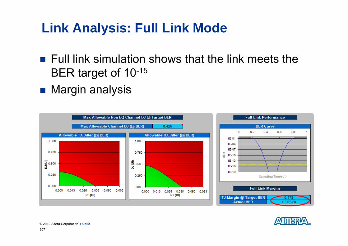
Link Analysis: Full Link Mode
Full link simulation shows that the link meets the BER target of 10-15
Margin analysisg y
© 2012 Altera Corporation Public207

EyeQ Enables On-Chip Analog Debug EyeQ is a circuit that enables users to “probe” the CDR input Users can view the eye opening at the CDR inputy p g p Users can see the correlation of EQ settings to eye opening EyeQ enables users to use the debug feature with live traffic
C t d ith C t d ith C t d ith
EyeQ®
Captured withOscilloscope
Captured withOscilloscope
Captured withTransceiver Toolkit
T itt O t t R i I tL Ch l
Pre-Emphasis EQ CDR
Minimize board bring up / debug time with Dynamic reconfiguration and EyeQ
Transmitter Output Receiver InputLossy Channel
© 2012 Altera Corporation Public208
Dynamic reconfiguration and EyeQ

EyeQ CircuitEyeQ Circuit
RX
EQ: EqualizerPD: Phase DetectorCP: Charge PumpVCO: Voltage Controlled OscillatorPI: Phase Interpolator
Sampler A
Multi -plexer
o
deserializerRecovered data
RX
OUT
p
RXInput EQ PD
CP VCO
CDR
1
64 vertical threshold levels 32 horizontal phase-
i t l t t
PI Multi -o
Recovered
EYEinterpolator steps 3ps / steps (@ 10Gbps)
User selectable threshold / PI settingPILogic
plexer
1
clock
VREF_GEN
BIT BitErr
PI setting
Sampler B
BIT Checker
BitErr
New in SV
© 2012 Altera Corporation Public209
New in SV

More Sophisticated ToolsDFT
DFT DFT Eye Diagram (Persistence mode) Eye Diagram (BER plot) BER Contours True Oscilloscope Capability Jitter Measurement Edge rates & Pre-emphasis
measurements and more …
© 2012 Altera Corporation Public210

SI Board Backplane Support Designed with mating BP
connector from each vendorAmphenolXcede
Molex Impact
Amphenol, Molex, Tyco
Can directly plug into vendor’s
p
Can directly plug into vendor s standard backplanes
Characterize performace at 10G & 12.1G
Tyco Strada Whisper(available soon)
Evaluate performance at higher data rates (ie 14 1G)
(available soon)
Stratix V SI Boardhigher data rates (ie, 14.1G)
© 2012 Altera Corporation Public211

High-Speed Transceiver Toolkit
© 2012 Altera Corporation—Public 3.0

High-Level Challenges – Debug Phases
Check if data is passing through transceiver channelPhase 1:Check if data is passing through transceiver channelduring PCB bring-up
Test BER by generating and verifying industry-standard PRBS data patterns
Dynamically reconfigure the pre-emphasis and equalization settings Analyze the link by using Stratix V EyeQ feature to find optimal settings y y g y p g
Phase 2:Perform in-system or mission-mode link analysis with real-time data in an operating hardware system
Integrate completed user design for full system testing Integrate completed user design for full system testing Verify BER by using Stratix V bit comparator
© 2012 Altera Corporation Public213

Debug Phase 1 – Q & A (1/3)
Can I see data in the transceiver channels?P f i l i l l b k Perform internal serial loopback
TX and RX loopback directly within the silicon
FPGA
© 2012 Altera Corporation Public214

Debug Phase 1 – Q & A (2/3)
Can I see data drive out of the FPGA TX pin and the d t d i b k i t th RX i d i ?same data drive back into the RX pin, and vice versa?
Perform external loopbackTX d RX d i i d t f th FPGA i TX and RX drive in and out of the FPGA pins
FPGA
© 2012 Altera Corporation Public215

Debug Phase 1 – Q & A (3/3)
Can I see data drive out of the FPGA TX pin and the d t i d i th d i t l t tsame data received in another device or external test
equipment, and vice versa? Perform reverse serial loopbackPerform reverse serial loopback TX from device 1 drives RX in device 2 and vice versa External test equipment drives RX in device 1 and vice versa
FPGA/ASIC/ASSPFPGA
© 2012 Altera Corporation Public216

Debug Phase 2 – Q & A
Can I see data running in the completed hardware system? Run final test by using the fully integrated user design
© 2012 Altera Corporation Public217

T i T lkit O iTransceiver Toolkit Overview
© 2012 Altera Corporation—Public

What is the Transceiver Toolkit?
The Transceiver Toolkit helps users generate d i t t l d t t t i d idesigns to control and test transceivers during PCB bring up or in-system signal integrity analysisanalysis
U il t l PMA tti t Users can easily control PMA settings, generate and check PRBS patterns to ensure optimal link operationoperation
B th d li d hi l i t f Both command line and graphical user interfaces are available
© 2012 Altera Corporation Public219

Transceiver Toolkit Features OverviewFeatures Description
Transceiver channels• Consist of full-duplex transmitter (TX) and receiver (RX) channelsE bl d di bl h t i h l• Enable and disable each transceiver channel
Dynamic reconfiguration• Change configuration (e.g. data rate, differential output voltage (VOD), pre- emphasis,
decision feedback equalizer (DFE), continuous-time linear equalizer (CTLE), and EyeQ) at run time
EyeQ • Draw BER bathtub curve and eye contour – Stratix V only
DFE • Enable decision feedback equalization (DFE) – Stratix V only
Data pattern generator and checker
• Change test patterns (e.g. pseudo-random binary sequence (PRBS)7, 15, 23, and 31) at run time
Auto sweep • Run sweep tests to converge optimal pre-emphasis and EyeQ settingsAuto sweep • Provide target BER for error check
Error insertion • Insert error on serial data in transceiver channel
Status • Indicate link lock, # of errors, # of transmitted data, and BER
Reporting • Report settings converged for different BER, equalization, and pre-emphasis
Diagnostics • Perform serial loopback and reverse serial loopback tests
© 2012 Altera Corporation Public220

G tti St t dGetting Started
© 2012 Altera Corporation—Public

Recommended User Flow (1/2)Download Example
Design
ModifyDesign?
Yes Apply Changes inQsysDesign?
Modify Yes
No
Change
Qsys
No
Modify Pins?
Yes Change Pin Assignments
Compile Design?
N
YesCompile Design
Program FPGA
No
© 2012 Altera Corporation Public

Recommended User Flow (2/2)Launch Transceiver
Toolkit
Create Links
Change SettingsManually
Auto Sweep BER and DFE
Auto Sweep EyeQEyeQ
Apply Optimal SettingsSettings
© 2012 Altera Corporation Public

PCB Set-Up
Power up PCB Check if FPGA was configured successfully Check if FPGA was configured successfully Make sure the links you want to test are connected
correctly (e.g. connect cables for external loopback h b l )shown below)
© 2012 Altera Corporation Public225

Board to Board
Transceiver ToolkitTransceiver Toolkit
DeviceDeviceZ
PCB 1Download
FPGA FPGA
Device C
Download Cable
Download Cable
FPGA FPGA C
DeviceB
Device A
FPGA FPGA
Multi-FPGA board to multi-FPGA b d t d i ti BA PCB 2board setup and communication
under 1 Transceiver Toolkit UI
© 2012 Altera Corporation Public226

Launch Transceiver ToolkitLaunch Transceiver
Toolkit
Create Links
Click Transceiver Toolkit from Tools menu in Quartus II
Change SettingsManually
Auto Sweep BER and DFE
Tools menu in Quartus II software
From System Explorer window,
Auto Sweep EyeQ
Apply Optimal Settingsy p
under “connections”, check list for your JTAG device If device name does not appear,
make sure the device is powered on and connected to the machine
Load Quartus II projectLoad Quartus II project containing transceiver design File Load Project
Open Transceiver Toolkit tab Open Transceiver Toolkit tab Tools Transceiver Toolkit
© 2012 Altera Corporation Public227

Connect to Targeted Device
Linking design instance to device:From System Explorer window navigate to “design instances” From System Explorer window, navigate to design_instances”
Right click on targeted instance Select your connected device
© 2012 Altera Corporation Public228

Create Tcl Set-Up ScriptLaunch Transceiver
Toolkit
Create Links
Automate set up
Change SettingsManually
Auto Sweep BER and DFE
Automate set-up using Tcl script Click Save As… from
Auto Sweep EyeQ
Apply Optimal Settings
Click Save As… from File menu
All saved scripts are shown under “scripts”shown under scripts
Click on a script
© 2012 Altera Corporation Public229

Create LinksLaunch Transceiver
Toolkit
Create Links
Transceiver Links tabThe channels in your design are auto populated in the
Change SettingsManually
Auto Sweep BER and DFE
The channels in your design are auto-populated in the Transmitter Channels and Receiver Channels tabs
By default, a link will be created between the transmitter and receiver of the same channel and shown in Transceiver
Auto Sweep EyeQ
Apply Optimal Settings
Links
© 2012 Altera Corporation Public230

Control Transceiver Link New Custom Control Panel (From QII 11.0 onwards)
Intelligent control management for improved ease of use Additional data reported – channel datarate, reference clock, LTD/LTR lock status Serial Loopback Control added Highly visible status indicators – color and animation
© 2012 Altera Corporation Public231

Improved Test Management Easily manage many parallel running BER tests Identify which channel resources are in use Quickly identify test run status (not started running running with problem)Quickly identify test run status (not started, running, running with problem)
© 2012 Altera Corporation Public232

Auto-Sweep BER TestsLaunch Transceiver
Toolkit
Create Links
Click Transceiver Auto Sweep Choose the Minimum and Maximum values for each setting (e.g.
VOD h i DC i li ti t )
Change SettingsManually
Auto Sweep BER and DFE
VOD, pre-emphasis, DC gain, equalization, etc.) Case count = number of different permutations will be performed Run length = conditions for stopping the auto-sweep (e.g. time limit
per permutation, error rate, etc.)
Auto Sweep EyeQ
Apply Optimal Settings
© 2012 Altera Corporation Public

Auto-Sweep BER Report
Create reports by clicking Create Report in the middle of the test or when the test completeswhen the test completes
Different columns show various transceiver settings All columns can be sorted
The report is exportable in a .csv format Right click on report, Select “Export…”
© 2012 Altera Corporation Public234

Auto-Sweep DFE Tests (Stratix V)Launch Transceiver
Toolkit
Create Links
1. Auto sweep with DFE off2 With best BER results lock down settings
Change SettingsManually
Auto Sweep BER and DFE
2. With best BER results, lock down settings (VOD, pre-emphasis, DC gain, equalization)
3. Then sweep with DFE settings to find best BER
Auto Sweep EyeQ
Apply Optimal Settings
BER
© 2012 Altera Corporation Public235

Auto-Sweep EyeQ Tests (Stratix V)Launch Transceiver
Toolkit
Create Links
Click Transceiver EyeQbutton on Transceiver Links
Change SettingsManually
Auto Sweep BER and DFE
button on Transceiver Linkstab to launch the EyeQwindow
Auto Sweep EyeQ
Apply Optimal Settings
Eye Contour automatically generated when sweep completes
Click Create Report to generate EyeQ reports
If you sort by BER column the If you sort by BER column, the number of rows with BER = 0 will be considered as the unit width of the eye from the specified physical media attachment (PMA) settings
© 2012 Altera Corporation Public

DDemo
© 2012 Altera Corporation—Public