xapp355: serial adc interface using a coolrunner cpld … · the ads7870 adc is a low power 12-bit,...
TRANSCRIPT

Summary This document describes the design implementation for controlling a Texas Instruments ADS7870 Analog to Digital Converter (ADC) in a Xilinx CoolRunner™ XPLA3™ CPLD. CoolRunner CPLDs are the lowest power CPLDs available and the ideal target device for controlling a serial ADC in a portable handheld application. This document provides an explanation of the VHDL code for the CoolRunner CPLD.
All related source code is provided for download. To obtain the VHDL code described in this document, go to section VHDL Code Download, page 27 for instructions.
Overview Figure 1 illustrates the high-level block diagram for the data aquisiton system. The system includes an XPLA3 CoolRunner CPLD, a Texas Instruments ADS7870 ADC, and a Toshiba SRAM. The Texas Instrument ADS7870 ADC is initialized and controlled by the CoolRunner CPLD. The CoolRunner CPLD takes conversion data from the ADC and writes the data to SRAM. The SRAM used in the Insight Handspring Springboard development board is a 4 Mbit Toshiba SRAM, TC55V400AFT. The Toshiba SRAM is a 16-bit word size SRAM, and is used for storing data in a conversion cycle. Once conversion data is written into SRAM, the CoolRunner CPLD allows the system processor to access the data.
Application Note: CoolRunner CPLD
XAPP355 (v1.1) January 3, 2002
Serial ADC Interface Using a CoolRunner CPLD
R
Figure 1: High Level Block Diagram
Texas
ADS7870
InstrumentsA/D Converter
CoolRunner XPLA3CPLD
Shift Data In
Shift Data Out
2.5 MHz CClk
SClk
A/D Control
AnalogInputs
8 Ch(4 Ch Diff.)
Dat
a
Ad
dre
ss
Toshiba4Mbit SRAM
Co
ntr
ol
XAPP355 (v1.1) January 3, 2002 www.xilinx.com 11-800-255-7778
© 2002 Xilinx, Inc. All rights reserved. All Xilinx trademarks, registered trademarks, patents, and disclaimers are as listed at http://www.xilinx.com/legal.htm. All other trademarks and registered trademarks are the property of their respective owners. All specifications are subject to change without notice.
Serial ADC Interface Using a CoolRunner CPLDR
Usage The VHDL code distributed with this document is designed such that minimal knowledge of VHDL language is required. A designated "constants" section of the VHDL code can be edited to specify various aspects of the ADS7870 which include:
• Initialization of internal registers
• Specification of the number of conversions for any (or all) of the eight single-ended channels
• Specification of SRAM locations where conversion results should be written
Designers who do not wish to understand the VHDL code in detail can simply edit this designated VHDL "constants" section, compile the design and program the CoolRunner CPLD. For more information, refer to section High Level Control Logic, page 6.
The following sections will detail the ADS7870 interface for those who wish to understand the VHDL implementation of the CPLD ADC interface.
For a complete Handspring design example, refer to "XAPP146: Designing an 8 Channel Digital Volt Meter with the Insight Springboard Kit".
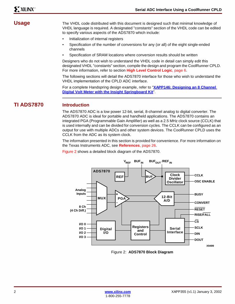
TI ADS7870 IntroductionThe ADS7870 ADC is a low power 12-bit, serial, 8-channel analog to digital converter. The ADS7870 ADC is ideal for portable and handheld applications. The ADS7870 contains an integrated PGA (Programmable Gain Amplifier) as well as a 2.5 MHz clock source (CCLK) that is used internally and can be divided for conversion cycles. The CCLK can be configured as an output for use with multiple ADCs and other system devices. The CoolRunner CPLD uses the CCLK from the ADC as its system clock.
The information presented in this section is provided for convenience. For more information on the Texas Instruments ADC, see References, page 26.
Figure 2 shows a detailed block diagram of the ADS7870.
Figure 2: ADS7870 Block Diagram
X9499
DigitalI/O
REF
VREF BUFIN BUFOUT /REF IN
ADS7870
Registersand
Control
SerialInterface
MUX PGA
BUF
12-BitA/D
I/O 0CS
CONVERT
RESET
BUSY
RISE/FALL
SCLK
DIN
ClockDivider
Oscillator
CCLK
OSC ENABLE
DOUT
+
-
AnalogInputs
8 Ch(4 Ch Diff.)
I/O 1I/O 2I/O 3
2 www.xilinx.com XAPP355 (v1.1) January 3, 20021-800-255-7778

Serial ADC Interface Using a CoolRunner CPLDR
Functional DescriptionEach functional block shown in Figure 2 in the ADS7870 is described in detail in Table 1.
Table 1: ADS7870 Functional Blocks
Block Description
MUX The ADS7870 has eight analog-signal input pins, LN0 through LN7. These input pins are connected to a multiplexer (a network of analog switches). This multiplexer is controlled by four bits in the Gain/Mux register.
LN0 through LN7 can each be configured as a single ended input or as a differential input. The M2 bit in the MUX address will enable the user to choose the polarity of the input.
The input signal at any of the LN0 through LN7 pins can range between –0.2V and 3.5V.
Clock Divider/Oscillator
CCLK, the conversion clock, is used by the A/D. CCLK can either function as an input pin (the user supplies an external clock) or an output pin (the ADS7870 will output a 2.5 MHz clock on the CCLK pin and use this signal as its conversion clock).
The OSC ENABLE pin controls whether CCLK is an input or an output. When pulled high, CCLK is an output. When OSC ENABLE = "0", the user may supply an external clock.
REF(Voltage Reference)
The Voltage Reference block can generate an output voltage of 1.15V, 2.048V, or 2.5V on the VREF pin.
In single-ended operation, the Voltage Reference will determine the maximum positive full scale input. For instance if VREF = 2.5V, an input of 2.5V will yield a result of +2047.
In differential mode, VREF will determine the center point. Register 7 controls whether the reference is turned on or off. On the Insight Springboard, the VREF pin is tied to the BUFIN pin.
BUF (Buffer Amplifier)
The Buffer Amplifier takes the internally generated Voltage Reference as an input and outputs it to the A/D block. A Buffer is used in order to increase the output current capability of the VREF pin.
The BUFE bit in Register 7 can turn the Buffer on or off. When the buffer is on, the ADS7870 will use the internal reference. If the Buffer is turned off, the ADS7870 will accept an external reference.
PGA(Programmable Gain Amplifier)
The PGA is a Programmable Gain Amplifier that can amplify the input signal before it is applied to the A/D Block. This is useful if the dynamic range of the input signal is small.
The PGA is capable of providing gains of 1, 2, 4, 5, 8, 10, 16, and 20 V/V.
The PGA gain is set by bits G2 through G0 of Register 4.
Serial Interface The ADS7870 communicates with the CoolRunner though this digital serial port interface. The serial interface is comprised of four pins: SCLK (Serial Data Clock), DIN (Serial Data Input), DOUT (Serial Data Output), and CS (Chip Select).
The RISE/FALL pin, also controlled by the CoolRunner, determines whether the ADS7870 will latch serial data on the rising or falling edge of SCLK. In this design, SCLK is active on the rising edge (the CoolRunner device always drives the RISE/FALL pin High).
XAPP355 (v1.1) January 3, 2002 www.xilinx.com 31-800-255-7778
Serial ADC Interface Using a CoolRunner CPLDR
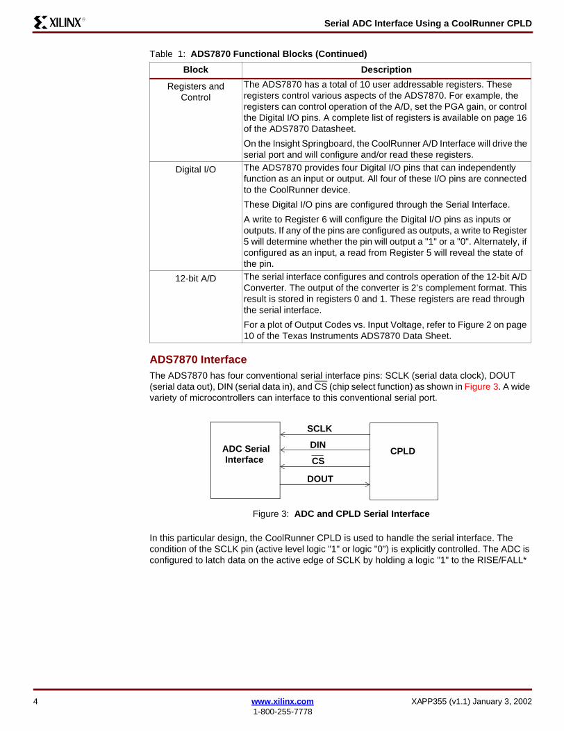
ADS7870 InterfaceThe ADS7870 has four conventional serial interface pins: SCLK (serial data clock), DOUT (serial data out), DIN (serial data in), and CS (chip select function) as shown in Figure 3. A wide variety of microcontrollers can interface to this conventional serial port.
In this particular design, the CoolRunner CPLD is used to handle the serial interface. The condition of the SCLK pin (active level logic "1" or logic "0") is explicitly controlled. The ADC is configured to latch data on the active edge of SCLK by holding a logic "1" to the RISE/FALL*
Registers and Control
The ADS7870 has a total of 10 user addressable registers. These registers control various aspects of the ADS7870. For example, the registers can control operation of the A/D, set the PGA gain, or control the Digital I/O pins. A complete list of registers is available on page 16 of the ADS7870 Datasheet.
On the Insight Springboard, the CoolRunner A/D Interface will drive the serial port and will configure and/or read these registers.
Digital I/O The ADS7870 provides four Digital I/O pins that can independently function as an input or output. All four of these I/O pins are connected to the CoolRunner device.
These Digital I/O pins are configured through the Serial Interface.
A write to Register 6 will configure the Digital I/O pins as inputs or outputs. If any of the pins are configured as outputs, a write to Register 5 will determine whether the pin will output a "1" or a "0". Alternately, if configured as an input, a read from Register 5 will reveal the state of the pin.
12-bit A/D The serial interface configures and controls operation of the 12-bit A/D Converter. The output of the converter is 2’s complement format. This result is stored in registers 0 and 1. These registers are read through the serial interface.
For a plot of Output Codes vs. Input Voltage, refer to Figure 2 on page 10 of the Texas Instruments ADS7870 Data Sheet.
Figure 3: ADC and CPLD Serial Interface
Table 1: ADS7870 Functional Blocks (Continued)
Block Description
SCLK
DIN
DOUT
CSADC Serial Interface
CPLD
4 www.xilinx.com XAPP355 (v1.1) January 3, 20021-800-255-7778

Serial ADC Interface Using a CoolRunner CPLDR
pin. Thus, the ADC interface ensures that data is available on the DIN pin when SCLK is "0" and holds it when SCLK is "1". Figure 4 illustrates this timing.
Control and configuration of the ADS7870 is accomplished by command bytes written to internal registers through the serial port. Command register device control includes MUX channel selection, PGA gain, and Reference Input control. One must use the “register mode” in order to configure a register.
Register Mode
In register mode, the first eight bits transmitted to the ADC specify the address of a particular register, whether to perform a read or a write operation and whether the data will be sixteen bits or eight bits. Immediately after these eight bits are sent, eight or 16 more bits (depending upon what was specified) are sent or received. For a write, data is sent through DIN. For a read, data will appear on the DOUT pin. For a complete list of available registers please refer to the ADS7870 datasheet. The VHDL code in this design allows the user to customize the register usage.
CS must remain Low in order to activate the serial interface. Once CS is brought Low, an internal counter residing in the ADS7870 begins counting the number of active SCLK edges. Raising the CS pin will put the DOUT pin in high impedance and will resynchronize the internal counter. It is possible to keep CS Low throughout an entire chain of serial commands (i.e., write to all address registers), but doing so will require careful management of the serial interface pins. One must be extremely careful when attempting to do so, as one error will cascade throughout the entire sequence.
Therefore, in this design, and in future designs, the CoolRunner CPLD briefly pulls the CS pin High after the completion of every serial command. This ensures that errors will not cascade.
Direct Mode
A conversion can be initiated on the ADS7870 by issuing a direct mode command. In this mode, a single 8-bit instruction byte is sent. The direct mode command will specify the input channel and the PGA gain. Immediately after this 8-bit instruction is sent, the ADS7870 will perform a conversion on the specified channel, with the specified PGA gain. The results will be written to Registers 0 and 1 and can be retrieved using a register mode read. However, in this design, the ADC is configured to use Read Back Mode 1. In this mode, the conversion result will automatically clock out on the next active edge of SCLK, after the last bit of the direct mode command is sent. Configuring the ADS7870 for Read Back Mode 1 will increase throughput since a separate read instruction is not required to read the result in registers 0 and 1.
CPLD Design Operational Flow
The CoolRunner CPLD controls the initialization of the ADC and the reading of conversion results. The CoolRunner CPLD then writes the conversion results of each conversion cycle to SRAM. This interface is implemented using two state machines. The state machines control the sending and receiving of parallel data and the configuring of internal ADC registers. After
Figure 4: ADC Serial Timing Diagram
SCLK
DIN data(7) data(6) data(1) data(0)
XAPP355 (v1.1) January 3, 2002 www.xilinx.com 51-800-255-7778

Serial ADC Interface Using a CoolRunner CPLDR
the CPLD initializes the ADC, it sends multiple "direct mode" instructions to initiate consecutive conversion cycles. The 12-bit serial data in a conversion cycle is read in by the CPLD and deserialized for a 16-bit word write to SRAM.
Figure 5 illustrates at a high level the operational flow for the ADC interface. The CPLD must initialize the ADS7870 registers that are pertinent to the design. This includes specifying each address register and the corresponding data to write. The CPLD then initializes the ADC for performing a "direct mode" conversion cycle for a specific input channel. The CPLD must send the direct mode command before reading out the ADC conversion data. The CPLD brings in the serial data and presents the deserialized data word to SRAM. The CPLD continues to issue the same direct mode command while reading the same input channel on the ADC. To read another input channel on the ADC a different direct mode instruction must be sent. The direct mode instruction includes control bits to specify the input channel on the ADC.
High Level Control LogicThe high level control logic for the ADC interface is implemented through the MAIN state machine. The state machine is responsible for sequencing through the following steps:
1. Specify the address of the register to be written.
2. Send the appropriate address over the serial interface.
Figure 5: ADC Interface Operational Flow
MoreChannels
?
No
Yes
END
START
Write to necessaryADC register
X355_05_080801
MoreRegisters
?
No
Yes
Start new conversion byissuing a direct mode command
for specified input channel
Read back conversion data
Write conversion data to SRAM
6 www.xilinx.com XAPP355 (v1.1) January 3, 20021-800-255-7778
Serial ADC Interface Using a CoolRunner CPLDR
3. Specify the data to write to the specified register.
4. Send the data via the serial interface to write.
5. Continue steps 1–4 until all registers have been initialized.
6. Specify direct mode instruction for a conversion on a specific input channel.
7. Read data in and deserialize for the conversion cycle.
8. Continue steps 6–7 until all data is read from the specific input channel.
9. Repeat steps 6–8 to read from all input channels that are specified and enabled.
To implement this functionality, the MAIN state machine as shown in Figure 6 has been designed and implemented. During the register mode states, the MAIN state machine specifies the parallel 8-bit data word to write to the ADC. The MAIN state machine loads the 8-bit data register and initiates the go_shift command. The SHIFT state machine, described in Shift Control Logic, page 11, takes the parallel data word and sends data out the serial interface to the ADC. The mode_flag signal is specified in the MAIN state machine for use by the SHIFT state machine.
XAPP355 (v1.1) January 3, 2002 www.xilinx.com 71-800-255-7778

Serial ADC Interface Using a CoolRunner CPLDR
.
Table 2 describes the functionality of each state in the MAIN state machine control logic shown in Figure 6. Note the mode_flag = "0" for the SHIFT control logic to designate the shift size for data. When mode_flag = "0", an 8-bit data value is shifted out. This is either a register address,
Figure 6: MAIN State Machine Control Logic
IDLE
WRITE_ADDR
Register Mode
Assert go_shift <= "1"& mode_flag = "0"
Assert go_shift <= "0"
Assert go_shift <= "1"
Assert go_shift <= "0"
WAIT_ADDR shift_done = "0"
shift_done = "1"
shift_done = "0"
shift_done = "1"
ADDR_DATA
WAIT_DATA
MoreRegisters
?
No
Yes
X355_06_080801
DIRECT_MODE
Direct Mode
Assert go_shift <= "1"
Assert go_shift <= "0"
Assert go_shift <= "1"& mode_flag = "1"
Assert go_shift <= "0"
WAIT_DM shift_done = "0"
shift_done = "1"
shift_done = "0"
shift_done = "1"
ASSIGN_DATA
READ_DATA
MoreConversion
Cycles?
Yes
No
DONE
8 www.xilinx.com XAPP355 (v1.1) January 3, 20021-800-255-7778

Serial ADC Interface Using a CoolRunner CPLDR
data to write to an address register, or the direct mode command. When mode_flag = "1", a 16-bit data value is shifted in from the ADC. This is for capturing the conversion data which consists of 12 bits of data, three zero bits, and the overflow bit.
Table 2: MAIN State Machine Description
State Functionality
IDLE Initializes specific combinatorial signals.
WRITE_ADDR Specifies the address of the register to write to. Loads the 8-bit shift register with this address. Asserts the go_shift signal to the SHIFT control logic to start shifting the address out. This state assigns wr_reg_num which specifies the address currently being written to for use in later states. State also deasserts the enable flag (which is TRUE for a write) for a specific register. Once the flag is disabled, the state machine will not write to that register again.
WAIT_ADDR Waits for SHIFT control logic to complete shifting out data to ADC on DIN. The signal shift_done will be asserted to represent this event.
ADDR_DATA Checks the value of wr_reg_num to compare which address was specified earlier to the ADC. The data to write to that register is loaded into the 8-bit shift register. Asserts the go_shift signal to the SHIFT control logic to start shifting data out.
WAIT_DATA Waits for SHIFT control logic to complete shifting out data to ADC on DIN. The signal shift_done will be asserted to represent this event. Checks to see if any remaining flags are set to TRUE, which indicates more registers need to be written to. The state machine then loops back to the WRITE_ADDR state. If all flags are set to FALSE, the state machine proceeds to the direct mode sequence.
DIRECT_MODE Specified the direct mode command to send to the ADC. Loads the 8-bit shift register with this direct mode command. Asserts the go_shift signal to the SHIFT control logic to start shifting the direct command out on DIN to the ADC. Based on direct mode command that is sent (which represents which input channel to read from), the SRAM address pointer is updated.
WAIT_DM Waits for SHIFT control logic to complete shifting out the direct mode command to ADC on DIN. The signal shift_done will be asserted to represent when the entire data word has been shifted out.
ASSIGN_DATA Sets mode_flag = "1". This signals the SHIFT control logic to count for 16 SCLK cycles to bring in the conversion data on DOUT. Asserts the go_shift signal to the SHIFT control logic to start counting the incoming data.
READ_DATA Waits for SHIFT control logic to assert shift_done to represent when the 16-bit conversion data is done being shifted into the system. Conversion data is written into SRAM at the specified location represented in sram_address. Checks if the sram_address is at the max address space for the specified ADC input channel. If so, then loops back to DIRECT_MODE for the next input channel. If not, then it loops back to DIRECT_MODE for the same input channel. If there remains no ADC input channels to read from, the state machine proceeds to the DONE state.
DONE End of state machine. Release control of bus to Handspring Visor.
XAPP355 (v1.1) January 3, 2002 www.xilinx.com 91-800-255-7778

Serial ADC Interface Using a CoolRunner CPLDR
Customizing the MAIN State MachineThe following is a description for customizing the MAIN state machine VHDL code for a specific application. The designation of register mode is for initializing the ADC registers. This allows the CPLD to configure the ADC. After, the ADS7870 has been configured, the MAIN state machine sends the "direct mode" command. Direct mode represents when the ADC is executing conversion cycles. The ADC will issue a direct mode command and then wait to receive the conversion data for the next 16 clock cycles.
Register Mode
The MAIN state machine continues to remain in the register mode, for initialization, until all registers have been set up and written to. The VHDL code enables the user to specify which registers to write to and the data to write to each register. The following VHDL code illustrates how to specify a write to ADDR3 in the ADC interface VHDL code.
constant WR_ADDR3_EN: BOOLEAN := TRUE;
-- Write/Read to Control Registerconstant ADDR3: STD_LOGIC_VECTOR(7 downto 0) := ’00000011’;
-- Data to be writtenconstant DATA_WR_ADDR3: STD_LOGIC_VECTOR(7 downto 0) := ’00000100’;
Note the variable WR_ADDR3_EN can be set to either TRUE or FALSE, enabling or disabling a write to ADDR3. If WR_ADDR3_EN is set to TRUE, then the data to write to that register must also be specified. This is done in the DATA_WR_ADDR3 constant. In this example, we are writing "0000 0100" to ADDR3, which specifies Read Back Mode 1 (MSB read back first) and sets CCLK division factor = 1. For more information on the data that can be written to each register, refer to References, page 26.
When writing to a register, not only is the register address specified, but additionally a read or write operation and the data word size can be specified.
The data written to the control registers allows the ADC to set up features such as: reading MSB or LSB first, the division factor of CCLK, PGA gain for a specific input channel, enabling the use of the digital I/O, and many more features that can be found in the ADC data sheet.
Direct Mode
Once all the control registers have been initialized in the ADC in the register mode, the ADC can now operate in the direct mode. The direct mode allows the external ADC controller to specify the input channel and read the conversion data. The VHDL code in this design has been constructed to ease the implementation for any application. The VHDL code enables the designer to specify which input channels to read from and how many conversions are requested on each input. The VHDL code for enabling/disabling register mode conversions is similar to the set up for register mode initialization. The following VHDL code illustrates how to perform eight conversions from the ADC single-ended input channel 0 and read eight conversions from the ADC single-ended input channel 1.
-- ********** DIRECT MODE CONVERSION SINGLE ENDED CHANNEL 0 ***************constant DM_SNG_LN0_EN : BOOLEAN := TRUE;constant DM_SNG_LN0 : STD_LOGIC_VECTOR(7 downto 0) := ’10001000’;constant SRAM_OFFSET0 : STD_LOGIC_VECTOR (22 downto 0) := ’00000000000000000000000’;constant SRAM_HIGH0 : STD_LOGIC_VECTOR (22 downto 0) := ’00000000000000000000111’;
-- *********** DIRECT MODE CONVERSION SINGLE ENDED CHANNEL 1 ************constant DM_SNG_LN1_EN : BOOLEAN := TRUE;constant DM_SNG_LN1 : STD_LOGIC_VECTOR(7 downto 0) := ’10001001’;
10 www.xilinx.com XAPP355 (v1.1) January 3, 20021-800-255-7778
Serial ADC Interface Using a CoolRunner CPLDR
constant SRAM_OFFSET1 : STD_LOGIC_VECTOR (22 downto 0) := ’00000000000000000001000’;constant SRAM_HIGH1 : STD_LOGIC_VECTOR (22 downto 0) := ’00000000000000000001111’;
The number of conversions in this particular example is controlled by counting each conversion write to SRAM. Therefore, once the address counter for the SRAM reaches the SRAM_HIGH offset, the specified number of conversions are counted. To enable a conversion from a specific input channel, the VHDL constant DM_SNG_LN0_EN set to TRUE will enable multiple conversions from LN0 in the ADC. Note that for only reading from one single-ended input channel, all other input channel enable constants must be set to FALSE. The constant DM_SNG_LN0 stores the value to send a direct mode command for a conversion on LN0. Refer to the ADS7870 data sheet for more information on sending a direct mode command.
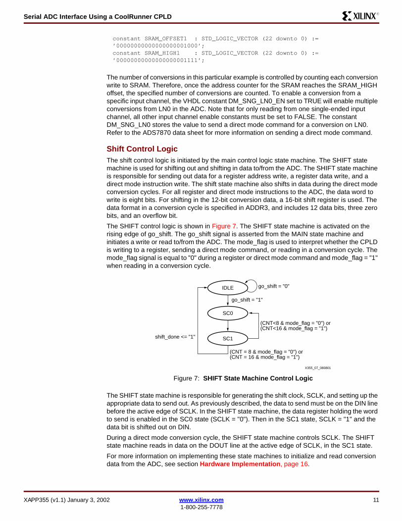
Shift Control LogicThe shift control logic is initiated by the main control logic state machine. The SHIFT state machine is used for shifting out and shifting in data to/from the ADC. The SHIFT state machine is responsible for sending out data for a register address write, a register data write, and a direct mode instruction write. The shift state machine also shifts in data during the direct mode conversion cycles. For all register and direct mode instructions to the ADC, the data word to write is eight bits. For shifting in the 12-bit conversion data, a 16-bit shift register is used. The data format in a conversion cycle is specified in ADDR3, and includes 12 data bits, three zero bits, and an overflow bit.
The SHIFT control logic is shown in Figure 7. The SHIFT state machine is activated on the rising edge of go_shift. The go_shift signal is asserted from the MAIN state machine and initiates a write or read to/from the ADC. The mode_flag is used to interpret whether the CPLD is writing to a register, sending a direct mode command, or reading in a conversion cycle. The mode_flag signal is equal to "0" during a register or direct mode command and mode_flag = "1" when reading in a conversion cycle.
The SHIFT state machine is responsible for generating the shift clock, SCLK, and setting up the appropriate data to send out. As previously described, the data to send must be on the DIN line before the active edge of SCLK. In the SHIFT state machine, the data register holding the word to send is enabled in the SC0 state (SCLK = "0"). Then in the SC1 state, SCLK = "1" and the data bit is shifted out on DIN.
During a direct mode conversion cycle, the SHIFT state machine controls SCLK. The SHIFT state machine reads in data on the DOUT line at the active edge of SCLK, in the SC1 state.
For more information on implementing these state machines to initialize and read conversion data from the ADC, see section Hardware Implementation, page 16.
Figure 7: SHIFT State Machine Control Logic
IDLE go_shift = "0"
go_shift = "1"
shift_done <= "1"
SC0
(CNT<8 & mode_flag = "0") or(CNT<16 & mode_flag = "1")
(CNT = 8 & mode_flag = "0") or(CNT = 16 & mode_flag = "1")
SC1
X355_07_080801
XAPP355 (v1.1) January 3, 2002 www.xilinx.com 111-800-255-7778
Serial ADC Interface Using a CoolRunner CPLDR
Allowing the Visor to Read Conversion Results
After conversion results have been written to SRAM, the Handspring Visor must be given access to read the conversion result from SRAM. This transfer of control occurs once the MAIN state machine has written all conversion results to SRAM. This is specified in the DONE state of the MAIN state machine.
This section will detail how the CoolRunner CPLD releases control of the bus to the Handspring Visor.
On the Insight Springboard Development Kit, all address, data and control signals originating from the Springboard expansion area are routed into the CoolRunner CPLD. These signals are then internally routed to a brand new set of pins, which are then externally connected to the SRAM, A/D, and Flash. XAPP147: "Low Power Handspring Springboard Module Design with CoolRunner CPLDs", illustrates this routing scheme. In the most basic case, the CoolRunner would simply act as a buffer for all signals, all signals would go directly into and then out of the CPLD, without being manipulated.
In this case, however, the functionality of the CoolRunner has increased because it has the added task of controlling the ADS7870. The CoolRunner must allow both the Visor and the A/D to be able to write (and read) to SRAM. Therefore, the simple interface shown in XAPP147 must be slightly modified to include multiplexers. These multiplexers are controlled by the ADS7870 interface. When the interface is active, the multiplexers allow for the CPLD to write conversion results to SRAM. When conversions are finished, the Visor is allowed to read these conversions from SRAM, or alternately write new values to SRAM.
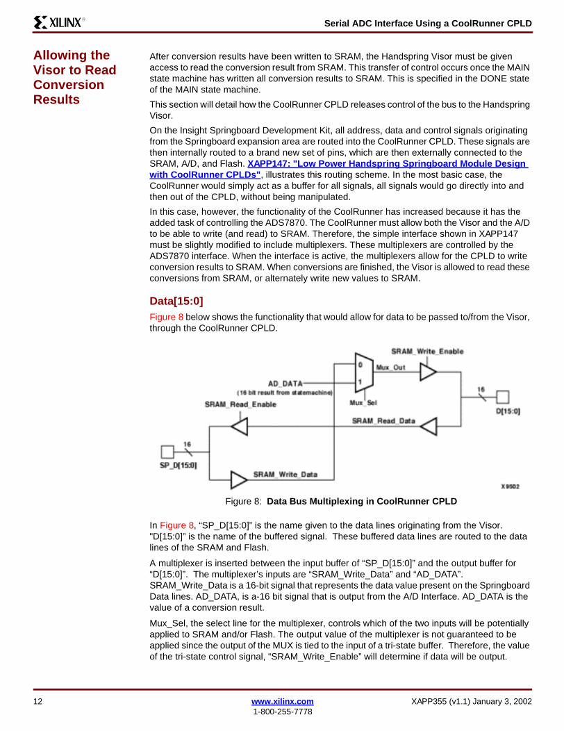
Data[15:0]Figure 8 below shows the functionality that would allow for data to be passed to/from the Visor, through the CoolRunner CPLD.
In Figure 8, “SP_D[15:0]” is the name given to the data lines originating from the Visor. "D[15:0]” is the name of the buffered signal. These buffered data lines are routed to the data lines of the SRAM and Flash.
A multiplexer is inserted between the input buffer of “SP_D[15:0]” and the output buffer for “D[15:0]”. The multiplexer’s inputs are “SRAM_Write_Data” and “AD_DATA”. SRAM_Write_Data is a 16-bit signal that represents the data value present on the Springboard Data lines. AD_DATA, is a-16 bit signal that is output from the A/D Interface. AD_DATA is the value of a conversion result.
Mux_Sel, the select line for the multiplexer, controls which of the two inputs will be potentially applied to SRAM and/or Flash. The output value of the multiplexer is not guaranteed to be applied since the output of the MUX is tied to the input of a tri-state buffer. Therefore, the value of the tri-state control signal, “SRAM_Write_Enable” will determine if data will be output.
Figure 8: Data Bus Multiplexing in CoolRunner CPLD
12 www.xilinx.com XAPP355 (v1.1) January 3, 20021-800-255-7778

Serial ADC Interface Using a CoolRunner CPLDR
When Mux_Sel is "0" the Handspring Visor will have control of the data lines. Alternately, when Mux_Sel is "1", the A/D Interface is allowed to write data to SRAM. The A/D Interface controls the value of Mux_Sel so that when it is active, the value of Mux_Sel will be "1" and when it is complete, the value will be set to "0".
SRAM_Write_Enable is a tri-state control signal that determines if the “D[15:0]” pins will function as an input or as an output. D[15:0] will function as outputs if the value of SRAM_Write_Enable is a "1". On the other hand, the D[15:0] pins will be inputs if the tri-state control signal is "0".
The SRAM_Write_Enable equation is equal to:
(SM_WE) + (SM_WE) & [ WE & (CS0 + CS1) ]
Table 3 describes each literal in the SRAM_Write_Enable equation.
In the SRAM_Write_Enable equation, the SM_WE literal is generated by the A/D Interface. SM_WE is declared to be "1" when the A/D interface is running, thereby making the entire equation equal to "1". This enables the output buffer and since MUX_Sel is "1" when the A/D Interface is active, the A/D conversion results can be written to SRAM.
When the conversions are complete, the A/D Interface declares SM_WE to be "0" and Mux_Sel to be "0" so that the Handspring can either read the conversion results stored in SRAM or write new data to SRAM.
Once the Visor is given control of the bus (i.e., SM_WE becomes "0"), the Visor can enable the output buffer by executing a write to SRAM. A write operation to an address between 0x29000000 and 0x29FFFFFF (the default memory mapped region for CS1) will cause CS1 and WE to become "0", making the SRAM_Write_Enable equation true.
If needed, the Visor may also write to the Flash memory region that corresponds to CS0 (address 0x28000000 to 0x28FFFFFF). Doing this will create a falling edge on CS0 and WE.
The Visor can retrieve contents in SRAM by executing a read operation. Once again, an output buffer will determine if the SP_D[15:0] pins will provide data to the Visor or if these pins will send data to external components. This output buffer is controlled by the SRAM_Read_Enable signal.
The equation for SRAM_Read_Enable is equal to:
OE & (CS0 + CS1)
If the Visor executes a read operation from SRAM, the CS1 and OE signals will go Low. The SP_D[15:0] pins will then be allowed to output data to the Visor.
Table 3: Literal Description
Literal Description Function
SM_WE Write Enable generated by A/D Interface "0" when A/D Interface is inactive"1" when A/D Interface is active
WE Write Enable signal generated by Visor "0" when Visor executes a write"1" when others
CS0 Chip Select 0 signal generated by Visor "0" when Visor writes or reads to CS0 memory region"1" when others
CS1 Chip Select 1 signal generated by Visor "0" when Visor writes or reads to CS1 memory region"1" when others
Notes: 1. By default, the CS0 memory region is mapped to address locations 0x28000000 to 0x28FFFFFF.
This region corresponds to the Flash address locations.2. By default, the CS1 memory region is mapped to address locations 0x29000000 to 0x29FFFFFF.
This region corresponds to the SRAM address locations.
XAPP355 (v1.1) January 3, 2002 www.xilinx.com 131-800-255-7778

Serial ADC Interface Using a CoolRunner CPLDR
Address LinesThe address lines originating from the Springboard Expansion Connector, “SP_A[23:1]”, are routed through the CoolRunner. The SP_A[23:1] pins are connected internally to one input of the address multiplexer, as shown in Figure 9. This Multiplexer has two inputs, one of which is SP_A[23:1] and the other which is ADDR_COUNT. MUX_SEL, the same select signal for the other multiplexers in this design, is used for the select line of this multiplexer.
A[23:1] is the output of this switch. This output bus is tied to external pins which are then routed to the address lines of Flash and SRAM. Figure 9 illustrates this.
When the A/D Interface is active, MUX_SEL is set to "1". This allows the value of SM_ADDRESS to determine the value of A[23:1].
The VHDL signal SM_ADDRESS is assigned for each write to SRAM. The value of SM_ADDRESS is initialized for a specific input channel as specified in the VHDL "constants" section discussed in section, Direct Mode, page 10. This address counter, SM_ADDRESS is increment for each subsequent write to SRAM. The ADC will stop reading from the current input channel once the SM_ADDRESS counter reaches the max address space for the current input channel.
The Digital Volt Meter design shown in Hardware Implementation, page 16 writes to address locations 0, 1, and 2 of SRAM for the ADC input channel 0.
Figure 9: Address MUX
Chip Select 1Figure 10 shows the Chip Select 1 multiplexer. A switch is needed in order to give the A/D Interface the ability to control the CS pin of the SRAM. The SRAM CS pin is an active Low signal that enables the SRAM chip. When CS is Low and RW (Write Enable) is Low, data will be written to SRAM. When CS is Low and OE (Output Enable) is Low, the SRAM will output data so a read operation can occur.
SPRING_CHIP1_ENn is the CS1 pin originating from the Visor’s expansion area. STATE_MACHINE_SRAM_ENn is an internal signal that is controlled by the A/D Interface. The SRAM_CHIP1_ENn signal is externally routed to the CS pin of the SRAM.
When the A/D Interface is active, MUX_SEL is "1" and hence the value of STATE_MACHINE_SRAM_EN determines the value of the CS pin on the SRAM. When the A/D Interface writes a conversion result to SRAM, it pulls the STATE_MACHINE_SRAM_EN signal and the STATE_MACHINE_WE (see next page) signal Low.
MUX_SEL
0
1
SP_A[23:1]23
A[23:1]23
SM_ADDRESS23
14 www.xilinx.com XAPP355 (v1.1) January 3, 20021-800-255-7778

Serial ADC Interface Using a CoolRunner CPLDR
After the conversions are complete, MUX_SEL is set to "0" and the Handspring Visor can once again perform its own read and write operations.
Write EnableFigure 11 shows the Write Enable Multiplexer. This multiplexer is needed in order to give the A/D Interface the ability to control the RW (Write Enable) pin of SRAM. The RW pin is an active low signal that, when used in conjunction with the CS pin, will enable a write operation to occur.
SPRING_WRITE_ENn is the Write Enable pin originating from the Visor’s expansion area. STATE_MACHINE_WE is an internal signal that is controlled by the A/D Interface. The output of the multiplexer, READ_WRITEn is externally routed to the RW pin of the SRAM.
When the A/D Interface is active, MUX_SEL is "1" and the value of STATE_MACHINE_WE will determine the value of the SRAM RW pin. When the A/D Interface writes a conversion result to SRAM, it pulls the STATE_MACHINE_WE signal Low and the STATE_MACHINE_SRAM_ENn signal low. (See Chip Select 1, page 14 for an explanation of the STATE_MACHINE_SRAM_ENn signal.
After the conversions are complete, MUX_SEL is set to "0" and the Handspring Visor can once again perform its own read and write operations.
Output EnableFigure 12 shows the Output Enable multiplexer. This multiplexer is needed in order to give the A/D Interface the ability to control the OE (Output Enable) pin of SRAM. The OE pin is an active low signal that, when used in conjunction with the CS pin, will allow a read operation to occur.
SPRING_OUTPUT_ENn is the Output Enable pin originating from the Visor’s expansion area. STATE_MACHINE_OE is an internal signal that is controlled by the A/D Interface. The output of the multiplexer, OUTPUT_ENn is externally routed to the OE pin of the SRAM.
When the A/D Interface is active, MUX_SEL is "1" and the value of STATE_MACHINE_OE will determine the value of the SRAM OE pin. When the A/D Interface writes a conversion result to SRAM, it pulls the STATE_MACHINE_OE signal Low and the STATE_MACHINE_SRAM_ENn signal Low. (See previous page for an explanation of the STATE_MACHINE_SRAM_ENn signal.)
Figure 10: Chip Select 1 MUX
Figure 11: Write Enable MUX
X9504MUX_SEL
0
1
SPRING_CHIP1_ENnSRAM_CHIP1_ENn
STATE_MACHINE_SRAM_ENn
X9505MUX_SEL
0
1
SPRING_WRITE_ENnREAD_WRITEn
STATE_MACHINE_WE
XAPP355 (v1.1) January 3, 2002 www.xilinx.com 151-800-255-7778

Serial ADC Interface Using a CoolRunner CPLDR
After the conversions are complete, MUX_SEL is set to "0" and the Handspring Visor can once again perform its own read and write operations.
Hardware Implementation
Usage ExampleThe following section is provided as an example for modifying the VHDL code to target a specific application. Assume that in this application, the user wants to configure ADDR3, ADDR5, ADDR6, and ADDR7 and that the ADS7870 must perform a conversion on all eight input channels.
The following VHDL register "constants" have been edited for the following hardware implementation. Note we are writing "0000 0100" to ADDR3, "0000 0101" to ADDR5, "0000 1111" to ADDR6, and "0011 1100" to ADDR7.
In the VHDL direct mode "constants" section, flags can be set to enable a single ended conversion on a specific input channel of the ADC. For example, the DM_SNG_LN0_EN constant is set to TRUE to enable a single ended conversion on input channel 0. To specify the SRAM address space for each input channel, the SRAM_OFFSET0 constant is set to "00000000000000000000000". SRAM_HIGH0 is set to "00000000000000000000111". This represents that eight samples of channel 0 will be written to SRAM. Due to the pipelined nature of the ADC, the conversion data stored at address 0 should be discarded. Therefore, SRAM address 1 will store the first sample of channel 0. Also note, the SRAM address specified in the VHDL code is 23 bits wide. This is because the Springboard address 0 (A0) is set to 0. This means that A0 is appended to the SRAM address, and data is written to SRAM locations 0, 2, 4, etc.
--***************** ADDR0 (ADC OUTPUT REGISTER) ******************-- Description: ADDR0 stores the LS Byte of the conversion result.-- R/W : READ ONLYconstant RD_ADDR0_EN: BOOLEAN := FALSE;constant ADDR0 : STD_LOGIC_VECTOR(7 downto 0) := ’01000000’; -- Read ADDR 0
--******************** ADDR1 (ADC OUTPUT REGISTER) ****************-- Description: ADDR1 stores the MS Byte of the converstion result-- R/W : READ ONLYconstant RD_ADDR1_EN: BOOLEAN := FALSE;constant ADDR1 : STD_LOGIC_VECTOR(7 downto 0) := ’01000001’; -- Read ADDR 1
--********************* ADDR2 (PGA VALID REGISTER) ***************-- Description: ADDR2 reveals if PGA has exceeded allowable values-- R/W : READ ONLYconstant RD_ADDR2_EN: BOOLEAN := FALSE;constant ADDR2 : STD_LOGIC_VECTOR(7 downto 0) := ’01000010’; -- Read ADDR2
--******************** ADDR3 (A/D CONTROL REGISTER) ***************-- Description: ADDR3 configures CCLK Divider and read back mode operation-- R/W : R/Wconstant WR_ADDR3_EN: BOOLEAN := TRUE;
Figure 12: Output Enable MUX
X9506MUX_SEL
0
1STATE_MACHINE_OE
OUTPUT_ENnSPRING_OUTPUT_ENn
16 www.xilinx.com XAPP355 (v1.1) January 3, 20021-800-255-7778

Serial ADC Interface Using a CoolRunner CPLDR
-- Write/Read to Control Registerconstant ADDR3 : STD_LOGIC_VECTOR(7 downto 0) := ’00000011’;
-- Data to be writtenconstant DATA_WR_ADDR3: STD_LOGIC_VECTOR(7 downto 0) := ’00000100’;
--********************* ADDR4 (GAIN/MUX REGISTER) ****************-- Description: ADDR4 configures the PGA gain and the input channel-- selection. (A direct mode operation will accomplish this as well)-- R/W : R/Wconstant WR_ADDR4_EN: BOOLEAN := FALSE;
-- Write/Read to Gain/Mux Registerconstant ADDR4 : STD_LOGIC_VECTOR(7 downto 0) := ’00000100’;
-- Data to be writtenconstant DATA_WR_ADDR4: STD_LOGIC_VECTOR(7 downto 0) := ’00000000’;
--****************** ADDR5 (DIGITAL I/O STATE REGISTER) ***************-- Description: ADDR5 sets/reveals the state of the digital IO pins.-- R/W : R/Wconstant WR_ADDR5_EN: BOOLEAN := TRUE;
-- Write/Read Digital I/O State Regconstant ADDR5 : STD_LOGIC_VECTOR(7 downto 0) := ’00000101’;
-- Data to be writtenconstant DATA_WR_ADDR5: STD_LOGIC_VECTOR(7 downto 0) := ’00000101’;
--**************** ADDR6 (DIGITAL I/O CONTROL REGISTER) ***************-- Description: ADDR6 determines whether each of the four IO pins will be-- an output or and output-- R/W : R/Wconstant WR_ADDR6_EN: BOOLEAN := TRUE;constant ADDR6 : STD_LOGIC_VECTOR(7 downto 0) := ’00000110’;constant DATA_WR_ADDR6: STD_LOGIC_VECTOR(7 downto 0) := ’00001111’;
--**************** ADDR7 (REF/OSCILLATOR CONTROL REGISTER)************-- Description: ADDR7 determines:-- a) Whether the internal oscillator is used for the conversion clock-- b) Whether the internal voltage reference and buffer are ON or OFF-- c) Whether the voltage reference is 2.5V, 2.048V or 1.15V-- R/W : R/W
constant WR_ADDR7_EN: BOOLEAN := TRUE;constant ADDR7 : STD_LOGIC_VECTOR(7 downto 0) := ’00000111’;constant DATA_WR_ADDR7: STD_LOGIC_VECTOR(7 downto 0) := ’00111100’;
--*************** ADDR24 (SERIAL INTERFACE CONTROL REGISTER) **********-- Description: ADDR24 allows certain aspects of the serial interface to be -- changed by the user-- R/W : R/Wconstant WR_ADDR24_EN: BOOLEAN := FALSE;
-- Serial Interface Controlconstant ADDR24 : STD_LOGIC_VECTOR(7 downto 0) := ’00011000’;constant DATA_WR_ADDR24: STD_LOGIC_VECTOR(7 downto 0) := ’00000000’;
--******************** ADDR31 (ID REGISTER) **********************-- Description: ADDR31 reveals which version of ADS7870 is being used-- R/W : READ ONLY
XAPP355 (v1.1) January 3, 2002 www.xilinx.com 171-800-255-7778

Serial ADC Interface Using a CoolRunner CPLDR
constant WR_ADDR31_EN: BOOLEAN := FALSE;
-- ID Registerconstant ADDR31 : STD_LOGIC_VECTOR(7 downto 0) := ’00011111’;
-- ********* DIRECT MODE CONVERSION SINGLE ENDED CHANNEL 0 ************constant DM_SNG_LN0_EN : BOOLEAN := TRUE;constant DM_SNG_LN0 : STD_LOGIC_VECTOR(7 downto 0) := ’10001000’; constant SRAM_OFFSET0 : STD_LOGIC_VECTOR (22 downto 0) := ’00000000000000000000000’;constant SRAM_HIGH0 : STD_LOGIC_VECTOR (22 downto 0) := ’00000000000000000000111’;
-- ********** DIRECT MODE CONVERSION SINGLE ENDED CHANNEL 1 *************constant DM_SNG_LN1_EN : BOOLEAN := TRUE;constant DM_SNG_LN1 : STD_LOGIC_VECTOR(7 downto 0) := ’10001001’; constant SRAM_OFFSET1 : STD_LOGIC_VECTOR (22 downto 0) := ’00000000000000000001000’;constant SRAM_HIGH1 : STD_LOGIC_VECTOR (22 downto 0) := ’00000000000000000001111’;
-- ********** DIRECT MODE CONVERSION SINGLE ENDED CHANNEL 2 *************constant DM_SNG_LN2_EN : BOOLEAN := TRUE;constant DM_SNG_LN2 : STD_LOGIC_VECTOR(7 downto 0) := ’10001010’; constant SRAM_OFFSET2 : STD_LOGIC_VECTOR (22 downto 0) := ’00000000000000000010000’;constant SRAM_HIGH2 : STD_LOGIC_VECTOR (22 downto 0) := ’00000000000000000010111’;
-- ********** DIRECT MODE CONVERSION SINGLE ENDED CHANNEL 3 *************constant DM_SNG_LN3_EN : BOOLEAN := TRUE;constant DM_SNG_LN3 : STD_LOGIC_VECTOR(7 downto 0) := ’10001011’; constant SRAM_OFFSET3 : STD_LOGIC_VECTOR (22 downto 0) := ’00000000000000000011000’;constant SRAM_HIGH3 : STD_LOGIC_VECTOR (22 downto 0) := "00000000000000000011111";
-- ********** DIRECT MODE CONVERSION SINGLE ENDED CHANNEL 4 **************constant DM_SNG_LN4_EN : BOOLEAN := TRUE;constant DM_SNG_LN4 : STD_LOGIC_VECTOR(7 downto 0) := ’10001100’; constant SRAM_OFFSET4 : STD_LOGIC_VECTOR (22 downto 0) := ’00000000000000000100000’;constant SRAM_HIGH4 : STD_LOGIC_VECTOR (22 downto 0) := ’00000000000000000100111’;
-- ********** DIRECT MODE CONVERSION SINGLE ENDED CHANNEL 5 **************constant DM_SNG_LN5_EN : BOOLEAN := TRUE;constant DM_SNG_LN5 : STD_LOGIC_VECTOR(7 downto 0) := ’10001101’; constant SRAM_OFFSET5 : STD_LOGIC_VECTOR (22 downto 0) := ’00000000000000000101000’;constant SRAM_HIGH5 : STD_LOGIC_VECTOR (22 downto 0) := "00000000000000000101111’;
-- ********** DIRECT MODE CONVERSION SINGLE ENDED CHANNEL 6 *************constant DM_SNG_LN6_EN : BOOLEAN := TRUE;constant DM_SNG_LN6 : STD_LOGIC_VECTOR(7 downto 0) := ’10001110’; constant SRAM_OFFSET6 : STD_LOGIC_VECTOR (22 downto 0) := ’00000000000000000110000’;constant SRAM_HIGH6 : STD_LOGIC_VECTOR (22 downto 0) := ’00000000000000000110111’;
-- ********* DIRECT MODE CONVERSION SINGLE ENDED CHANNEL 7 **************
18 www.xilinx.com XAPP355 (v1.1) January 3, 20021-800-255-7778

Serial ADC Interface Using a CoolRunner CPLDR
constant DM_SNG_LN7_EN : BOOLEAN := TRUE;constant DM_SNG_LN7 : STD_LOGIC_VECTOR(7 downto 0) := ’10001111’; constant SRAM_OFFSET7 : STD_LOGIC_VECTOR (22 downto 0) := ’00000000000000000111000’;constant SRAM_HIGH7 : STD_LOGIC_VECTOR (22 downto 0) := ’00000000000000000111111’;
ADC Initialization (Register Mode)Using these VHDL "constants", the following ADC interface will be implemented:
1. Write data to Address 3, the “ADC Control Register” (ends with first rising edge of CS).
2. Write data to Address 6, the “Digital I/O Control Register” (ends with second rising edge of CS).
3. Write data to Address 5, the “Digital I/O State Register” (ends with third rising edge of CS).
4. Write data to Address 7, the “Reference Oscillator Register” (ends with fourth rising edge of CS).
5. Initiate three consecutive conversions on ADC input channel 0.
Note that CS goes High and SCLK temporarily stops in between commands (i.e., whenever data has been written to ADDR3, ADDR6, and ADDR5). This is done because a rising edge on CS will resynchronize the serial interface.
Note that in the beginning, DOUT tends to follow the CS pin. This is expected because of two factors: first, the DOUT pin enters high impedance when CS is held High and second, the DOUT pin is externally pulled up.
Step 1: Writing to ADDR3
Upon reset, the state machine will execute a register mode write to Address 3, the ADC Control Register (See ADS7870 Datasheet). A value of DIN = “0000 0100” written to ADDR3 will configure the A/D for Read Back Mode 1. In this mode, the serial interface configures itself to clock out a conversion result as soon as a conversion is started. A read instruction is not required to retrieve the result, thereby increasing the throughput rate by saving eight SCLK cycles. The very first data read back will be discarded, but subsequent values pipeline the conversion and readback activities.
This sequence requires a total of 16 SCLK cycles — eight bits to specify the Address, and eight more to write data to that address. After these 16 bits are sent, the state machine will enter a
XAPP355 (v1.1) January 3, 2002 www.xilinx.com 191-800-255-7778

Serial ADC Interface Using a CoolRunner CPLDR
wait state to resynchronize the serial interface. In this wait state, SCLK remains Low, and CS is momentarily raised High. Figure 13 shows a logic analyzer trace of this sequence.
Step 2: Writing to ADDR6
After exiting a wait state, the state machine executes a register mode write to Address 6, the Digital I/O Control Register (See page 19 of A/D Datasheet). The ADS7870 configures all four digital I/O pins as outputs by writing a data value of “0000 1111”.
As above,16 more SCLK cycles are required, followed by a wait state, to resynchronize the serial port. Figure 14 shows a logic analyzer trace of this sequence.
Figure 13: Writing to ADDR3
20 www.xilinx.com XAPP355 (v1.1) January 3, 20021-800-255-7778

Serial ADC Interface Using a CoolRunner CPLDR
Step 3: Writing to ADDR5
Next, the value of each I/O pin is configured to output a "1" or a "0". A pattern of DIN = “0000 0110” is transmitted to initiate an 8-bit write to Address 5, the Digital I/O State Register. The ADS7870 will then output a "0" on I/O1, a "1" on I/O2, a "0" on I/O3, and a "1" on I/O4 by sending “0000 0101” on the next sequence on DIN.
In this example, this test case is used with the Insight Handspring Development Board. Since all four Digital I/O pins are routed into the CoolRunner CPLD, they are used to control the four LEDs on the Insight Springboard Development Card. If the serial interface is working properly, the LEDs should read On, Off, On, Off.
Writing to this register requires another sixteen SCLK cycles and a wait state. Note that it is not absolutely necessary to write to ADDR6 and ADDR5. These two registers do not affect the conversion result. However, these registers have been configured to illustrate how to use the serial interface. In addition, they provide a convenient way to check the serial interface through the LEDs. A logic analyzer trace of this sequence is provided below in Figure 15.
Figure 14: Writing to ADDR6
XAPP355 (v1.1) January 3, 2002 www.xilinx.com 211-800-255-7778

Serial ADC Interface Using a CoolRunner CPLDR
Step 4: Writing to ADDR7
The Reference/Oscillator Register, ADDR7, configures the reference and the buffer (page 19 of ADS7870 Datasheet). After a pattern of “0000 0111” is sent to specify an 8-bit write to ADDR7, a sequence of “0011 1100” is written to this register.
The OSCR and OSCE bits are now set to "1". Enabling the OSCE bit will power the internal oscillator, and CCLK will output a 2.5 MHz signal. Setting the OSCR bit configures the ADS7870 to use this 2.5 MHz internal clock for the reference. The REFE and BUFE bits are also enabled. This turns on the Reference and the Buffer. And finally, by setting R2V and RBG bits to "0", VREF is set to 2.5V. This sets the maximum full-scale input to 2.5V in single ended
Figure 15: Writing to ADDR5
22 www.xilinx.com XAPP355 (v1.1) January 3, 20021-800-255-7778

Serial ADC Interface Using a CoolRunner CPLDR
mode. Sixteen more SCLK cycles and a wait state are needed, and a logic analyzer trace of this sequence is shown in Figure 16.
Direct Mode Conversions
Direct Mode Command 1
At this point, all registers have been properly configured, and the state machine is ready to send the first direct mode command to initiate a single conversion. Assuming that the LN0 input (an analog input of the ADS7870) is tied to the voltage site (test point), eight bits, “1000 1000” are sent through the DIN pin. This commands the A/D to start a conversion on input channel LN0, which has been configured as single ended, with the PGA (Programmable Gain Amplifier) gain set to "1".
Since Address 3 is configured for Read Back Mode 1, the ADS7870 will begin clocking out the result of the previous conversion immediately after the 8-bit direct mode command. Therefore, 16 more SCLK cycles are sent to the ADS7870. Thus, for this entire sequence, a total of 24 SCLK cycles are needed, eight for the direct mode command, and 16 for the result.
Note however, that on the last 16 clock cycles, DOUT remains Low. This is expected. Remember that the first result coming out of the ADS7870 is always invalid, due to the fact that the result is from the previous conversion.
Figure 17 actually shows more than 24 SCLK cycles instead of the 16 SCLK cycles that have been shown in the previous figures. This is done in order to show BUSY going High and then Low after the first direct mode command.
Figure 16: Writing to ADDR7
XAPP355 (v1.1) January 3, 2002 www.xilinx.com 231-800-255-7778

Serial ADC Interface Using a CoolRunner CPLDR
In reality, when we are chaining several conversions together, the CoolRunner does not need to monitor the BUSY pin. BUSY is shown just to confirm that a conversion is taking place.
Direct Mode Command 2
The second direct mode command is issued on the next rising edge of SCLK (i.e., on the 25th clock edge starting from when the first direct mode command sequence was issued).
Again, 24 SCLK cycles are needed for this second frame. The same 8-bit direct mode command of “1000 1000” is sent, but this time, notice that DOUT is driving data. This data is
Figure 17: Direct Mode Command 1
24 www.xilinx.com XAPP355 (v1.1) January 3, 20021-800-255-7778

Serial ADC Interface Using a CoolRunner CPLDR
the result of the first conversion. The result of this second conversion is returned in the next frame as shown in Figure 18. .
Within the frame of this example, DOUT reads “0000 1001 1011 0000”. Since the ADS7870 is set for Read Back Mode 1, the MS Byte of the conversion result is returned first. In other words, ADDR1 will clock out first, followed by ADDR0. (The Texas Instruments ADS7870 datasheet provides details of ADDR1 and ADDR0).
The 12-bit output code in this example is “0000 1001 1011”. This is equal to +155. The corresponding measured voltage would then equal:
(155 / 2047) * 2.5 = 0.189 Volts
It may also be of interest to see that this second direct mode command was issued when the first conversion was still in progress (Note the BUSY pin). The ADS7870 places this next
Figure 18: Direct Mode Command 2
Table 4: Contents of ADDR1, the MS Byte
D7 D6 D5 D4 D3 D2 D1 D0
ADC11 ADC10 ADC9 ADC8 ADC7 ADC6 ADC5 ADC4
0 0 0 0 1 0 0 1
Table 5: Contents of ADDR2, the LS Byte
D7 D6 D5 D4 D3 D2 D1 D0
ADC3 ADC2 ADC1 ADC0 0 0 0 OVR
1 0 1 1 0 0 0 0
XAPP355 (v1.1) January 3, 2002 www.xilinx.com 251-800-255-7778

Serial ADC Interface Using a CoolRunner CPLDR
conversion in queue and allows the current conversion to finish. Maximum throughput is obtained through this method, as the next conversion will begin immediately after the previous one finished. Again, note how the BUSY pin goes low then high during the conversion cycle.
Direct Mode Command 3
Figure 19 shows the third direct mode command. Like the previous direct mode command, this frame initiates a third consecutive conversion and retrieves the result of the second conversion.
Note, only three direct mode conversion cycles are shown for single ended input channel LN0. The implemented design allows for eight direct mode conversion cycles on each input channel of the ADC.
Conclusion The ADS7870 interface presented in this document is an easy to use reference design that will allow for quick customizing of the Insight Springboard Development Card. Regardless of whether a designer understands the VHDL language, the designated "constants" section of the VHDL code can be modified to configure the ADS7870 in a way that best complements a specific Springboard design. After modification, simply implement the design and program the CoolRunner CPLD. The inherent low power characteristics of the CoolRunner CPLD will come at no cost, and users will recognize the advantages of programmable logic.
References Texas Instruments ADS7870 Data Sheet located at http://www.ti.com/
Figure 19: Direct Mode Command 3
26 www.xilinx.com XAPP355 (v1.1) January 3, 20021-800-255-7778

Serial ADC Interface Using a CoolRunner CPLDR
VHDL Code Download
VHDL source code and test benches are available for this design. THE DESIGN IS PROVIDED TO YOU "AS IS". XILINX MAKES AND YOU RECEIVE NO WARRANTIES OR CONDITIONS, EXPRESS, IMPLIED, STATUTORY OR OTHERWISE, AND XILINX SPECIFICALLY DISCLAIMS ANY IMPLIED WARRANTIES OF MERCHANTABILITY, NON-INFRINGEMENT, OR FITNESS FOR A PARTICULAR PURPOSE. While this design has been verified on hardware, it should be used only as an example design, not as a fully functional core. XILINX does not warrant the performance, functionality, or operation of this design will meet your requirements, or that the operation of the design will be uninterrupted or error free, or that defects in the design will be corrected. Furthermore, XILINX does not warrant or make any representations regarding use or the results of the use of the design in terms of correctness, accuracy, reliability or otherwise.
XAPP355 - http://www.xilinx.com/products/xaw/coolvhdlq.htm
Revision History
The following table shows the revision history for this document.
Date Version Revision
09/25/01 1.0 Initial Xilinx release.
01/03/02 1.1 Minor revisions.
XAPP355 (v1.1) January 3, 2002 www.xilinx.com 271-800-255-7778