x7spa-l 1.2a manual
DESCRIPTION
Supermicro X7SPA-L 1.2a ManualTRANSCRIPT

Chapter 2: Installation
2-1
Chapter 2
Installation
2-1 Static-Sensitive Devices
Electrostatic-Discharge (ESD) can damage electronic com ponents. To pre-vent damage to your system board, it is important to handle it very carefully. The following measures are generally sufficient to protect your equipment from ESD.
Precautions• Use a grounded wrist strap designed to prevent static discharge.
• Touch a grounded metal object before removing the board from the antistatic bag.
• Handle the board by its edges only; do not touch its components, peripheral chips, memory modules or gold contacts.
• When handling chips or modules, avoid touching their pins.
• Put the motherboard and peripherals back into their antistatic bags when not in use.
• For grounding purposes, make sure your computer chassis provides excellent conductivity between the power supply, the case, the mounting fasteners and the motherboard.
• Use only the correct type of onboard CMOS battery. Do not install the onboard upside down battery to avoid possible explosion.
UnpackingThe motherboard is shipped in antistatic packaging to avoid static damage. When unpacking the board, make sure the person handling it is static protected.

2-2
X7SPA and X7SPE Motherboard Series User's Manual
MH
2
MH
3M
H4
D17
JPW1
JUSB
1
JD1
JPC3
JPUSB1
JWD
1
JPG1 JBMC1JPL1
JPT1
JPL2
JDIM
M2
1
JDIM
M1
JI2C
2
JI2C1JOH1JL1
JL2
SP1+
J2
J3
JBT1
JBAT1
JPCIE1
JUSB
5
JUSB4
JUSB3
JUSB
2
JLPC80
R105
0
JSMB1
FAN1 FAN2
JCO
M2
JCO
M4
JPI2C1
JWF1
J8
JVGA1
CD1
JPB
FAN
FAN
COMS CLEAR
2-3
DIS
ABL
E1-
2 EN
ABL
EJP
B:BM
C EN
ABL
E/D
ISA
BLE
CD-in
JPT1
:TPM
EN
ABL
E/D
ISA
BLE
1-2
ENA
BLE
2-3
DIS
ABL
E
AUDIO FP
T-SGPIO2 T-SGPIO1
JPI2
C:PW
R I2
C
JSMB1:SMBus1
JPU
SB1:
USB
WA
KE U
P
2-3
DIS
ABL
E1-
2 EN
ABL
E
JWF1
:DO
M P
WR
JD1:
1-3
PWR
LED
4-7
SPEA
KER
ON:ENABLEJI2C2OFF:DISABLE
JI2C1OFF:DISABLEON:ENABLE
JL2:
AUD
IO F
RON
T PA
NEL
SEL
ECT
ON
:AC'
97 F
RON
T PA
NEL
OFF
:HD
AU
DIO
FRO
NT
PAN
ELJP
G1:
VGA
2-3
DIS
ABL
E1-
2 EN
ABL
E2-
3 D
ISA
BLE
JPL2
:1-2
EN
ABL
E
JPL1
:1-2
EN
ABL
E2-
3 D
ISA
BLE
JL1:
CHA
SISS
INTR
USI
ON
JF1
PWR
ON
RST
X O
H/F
F N
IC2
NIC
1 H
DD
LED
PW
R LE
D X
NM
I
2-3
NM
IJW
D1:
1-2
RST
JBT1:
LAN2
LAN1
I-SATA5
I-SATA2
I-SATA4
I-SATA1
I-SATA3
I-SATA0
SLOT1 PCI-E X4 (IN X16 SLOT)
SYS
CPUKB/MOUSE
COM
4
COM
3
COM
2
COM1
SOD
IMM
2
SOD
IMM
1
CPU
J6J5
J10 J11
J12
J13
J14
JPF
2-2 Motherboard Installation
All motherboards have standard mounting holes to fit different types of chassis. Make sure that the locations of all the mounting holes for both motherboard and chassis match. Although a chassis may have both plastic and metal mounting fas-teners, metal ones are highly recommended because they ground the motherboard to the chassis. Make sure that the metal standoffs click in or are screwed in tightly. Then use a screwdriver to secure the motherboard onto the motherboard tray.
Caution: Some components are very close to the mounting holes. Please take precautionary measures to prevent damage to these components when installing the motherboard to the chassis.
Tools Needed
Philips Screwdriver Pan head screws (4-6 pieces)
Location of Mounting HolesThere are four (4) mounting holes on the X7SPA series, and six (6) on the X7SPE series motherboard.
Stand Offs (4-6 pieces)(Only if needed)
Note: The above items are not provided with this motherboard.
X7SPE Series Only

Chapter 2: Installation
2-3
Installation InstructionsInstall the I/O shield into the chassis.
Caution: To avoid damaging the motherboard and its components, please do not use a force greater than 8 lb/inch on each mounting screw during motherboard installation.
Locate the mounting holes on the motherboard. Refer to the layout on the previous page for mounting hole locations.
Locate the matching mounting holes on the chassis. Install standoffs in the chassis as needed. Align the mounting holes on the motherboard against the mounting holes on the chassis.
Install the motherboard into the chassis carefully to avoid damage to mother-board components.
Insert a Pan head #6 screw into a mounting hole on the motherboard and its matching mounting hole on the chassis, using the Philips screwdriver.
Repeat Step 4 to insert #6 screws to all mounting holes.
I/O Shield
1
23
Stand Off
45
6Make sure that the motherboard is securely placed on the chassis.7

2-4
X7SPA and X7SPE Motherboard Series User's Manual
Installing and Removing DIMMs
Memory Bank
MH
2
MH
3M
H4
D17
JPW1
JUSB
1
JD1
JPC3
JPUSB1
JWD
1
JPG1 JBMC1JPL1
JPT1
JPL2
JDIM
M2
1
JDIM
M1
JI2C
2
JI2C1JOH1JL1
JL2
SP1+
J2
J3
JBT1
JBAT1
JPCIE1
JUSB
5
JUSB4
JUSB3
JUSB
2
JLPC80
R105
0
JSMB1
FAN1 FAN2
JCO
M2
JCO
M4
JPI2C1
JWF1
J8
JVGA1
CD1
JPB
FAN
FAN
COMS CLEAR
2-3
DIS
ABL
E1-
2 EN
ABL
EJP
B:BM
C EN
ABL
E/D
ISA
BLE
CD-in
JPT1
:TPM
EN
ABL
E/D
ISA
BLE
1-2
ENA
BLE
2-3
DIS
ABL
E
AUDIO FP
T-SGPIO2 T-SGPIO1
JPI2
C:PW
R I2
C
JSMB1:SMBus1
JPU
SB1:
USB
WA
KE U
P
2-3
DIS
ABL
E1-
2 EN
ABL
E
JWF1
:DO
M P
WR
JD1:
1-3
PWR
LED
4-7
SPEA
KER
ON:ENABLEJI2C2OFF:DISABLE
JI2C1OFF:DISABLEON:ENABLE
JL2:
AUD
IO F
RON
T PA
NEL
SEL
ECT
ON
:AC'
97 F
RON
T PA
NEL
OFF
:HD
AU
DIO
FRO
NT
PAN
ELJP
G1:
VGA
2-3
DIS
ABL
E1-
2 EN
ABL
E2-
3 D
ISA
BLE
JPL2
:1-2
EN
ABL
E
JPL1
:1-2
EN
ABL
E2-
3 D
ISA
BLE
JL1:
CHA
SISS
INTR
USI
ON
JF1
PWR
ON
RST
X O
H/F
F N
IC2
NIC
1 H
DD
LED
PW
R LE
D X
NM
I
2-3
NM
IJW
D1:
1-2
RST
JBT1:
LAN2
LAN1
I-SATA5
I-SATA2
I-SATA4
I-SATA1
I-SATA3
I-SATA0
SLOT1 PCI-E X4 (IN X16 SLOT)
SYS
CPUKB/MOUSE
COM
4
COM
3
COM
2
COM1
SOD
IMM
2
SOD
IMM
1
CPU
J6J5
J10 J11
J12
J13
J14
JPF
2-3 System Memory
CAUTION Exercise extreme care when installing or removing DIMM modules to prevent any possible damage.
How to Install SO DIMMsInsert the desired number of SO DIMMs into the memory slots, starting with 1. DIMM1, then DIMM2. Pay attention to the notch along the bottom of the mod-ule to prevent incorrect DIMM module installation.
Insert each DIMM module at an angle vertically and snap it into place. Repeat 2. step 1 to install DIMM2 if needed. See instructions on the next page.
Memory SupportThe X7SPA-L, X7SPA-H, X7SPA-HF, X7SPE-H and X7SPE-HF supports up to 4GB of unbuffered Non-ECC DDR2 SODIMMs (667/800 MHz in 2 SO DIMM slots) while the X7SPE-H-D525, X7SPA-H-D525, X7SPA-HF-D525 and X7SPE-HF-D525 supports up to 4GB of unbuffered Non-ECC DDR3 SODIMMs (800MHz in 2 SO DIMM slots).
Note: Check the Supermicro website for a list of memory modules that have been validated with the X7SPA and X7SPE motherboard series.
MH
2
MH
3M
H4
D17
JPW1
JUSB
1
JD1
JPC3
JPUSB1
JWD
1
JPG1 JBMC1JPL1
JPT1
JPL2
JDIM
M2
1
JDIM
M1
JI2C
2
JI2C1JOH1JL1
JL2
SP1+
J2
J3
JBT1
JBAT1
JPCIE1
JUSB
5
JUSB4
JUSB3
JUSB
2
JLPC80
R105
0
JSMB1
FAN1 FAN2
JCO
M2
JCO
M4
JPI2C1
JWF1
J8
JVGA1
CD1
JPB
FAN
FAN
COMS CLEAR
2-3
DIS
ABL
E1-
2 EN
ABL
EJP
B:BM
C EN
ABL
E/D
ISA
BLE
CD-in
JPT1
:TPM
EN
ABL
E/D
ISA
BLE
1-2
ENA
BLE
2-3
DIS
ABL
E
AUDIO FP
T-SGPIO2 T-SGPIO1
JPI2
C:PW
R I2
C
JSMB1:SMBus1
JPU
SB1:
USB
WA
KE U
P
2-3
DIS
ABL
E1-
2 EN
ABL
E
JWF1
:DO
M P
WR
JD1:
1-3
PWR
LED
4-7
SPEA
KER
ON:ENABLEJI2C2OFF:DISABLE
JI2C1OFF:DISABLEON:ENABLE
JL2:
AUD
IO F
RON
T PA
NEL
SEL
ECT
ON
:AC'
97 F
RON
T PA
NEL
OFF
:HD
AU
DIO
FRO
NT
PAN
ELJP
G1:
VGA
2-3
DIS
ABL
E1-
2 EN
ABL
E2-
3 D
ISA
BLE
JPL2
:1-2
EN
ABL
E
JPL1
:1-2
EN
ABL
E2-
3 D
ISA
BLE
JL1:
CHA
SISS
INTR
USI
ON
JF1
PWR
ON
RST
X O
H/F
F N
IC2
NIC
1 H
DD
LED
PW
R LE
D X
NM
I
2-3
NM
IJW
D1:
1-2
RST
JBT1:
LAN2
LAN1
I-SATA5
I-SATA2
I-SATA4
I-SATA1
I-SATA3
I-SATA0
SLOT1 PCI-E X4 (IN X16 SLOT)
SYS
CPUKB/MOUSE
COM
4
COM
3
COM
2
COM1
SOD
IMM
2
SOD
IMM
1
CPU
J6J5
J10 J11
J12
J13
J14
JPFDIMM1
DIMM2

Chapter 2: Installation
2-5
Insert the SO DIMM module vertically at about a 45 degree angle.
To Remove: Use your thumbs to gently push the side clips near both ends away from the module. This should release it from the slot. Pull the SO DIMM module upwards.
The SO DIMM Socket
Position the SO DIMM module's bottom key so it aligns with the receptive point on the slot.
Press down until the module locks into place. The side clips will automatically secure the SO DIMM module, locking it into place.
1
2
3
4
Insert this end first
Press down until the module locks into place.
Locking clip
Locking clip
Align

2-6
X7SPA and X7SPE Motherboard Series User's Manual
I/O Port Locations and Definitions
2-4 Connectors/I/O Ports
The I/O ports are color coded in conformance with the PC 99 specification. See the figure below for the colors and locations of the various I/O ports.
Back Panel Connectors and I/O Ports
2 4
71 3 5 6 8
1. Keyboard (Purple)2. PS/2 Mouse (Green)3. USB Port 1/24. USB Port 3/4 (Supported on the X7SPA-L only)5. COM 1 (Green)6. VGA (Blue)7. LAN18. LAN 2 (NOT supported on the X7SPA-L)
MH
2
MH
3M
H4
D17
JPW1
JUSB
1
JD1
JPC3
JPUSB1
JWD
1
JPG1 JBMC1JPL1
JPT1
JPL2
JDIM
M2
1
JDIM
M1
JI2C
2
JI2C1JOH1JL1
JL2
SP1+
J2
J3
JBT1
JBAT1
JPCIE1
JUSB
5
JUSB4
JUSB3
JUSB
2
JLPC80
R105
0
JSMB1
FAN1 FAN2
JCO
M2
JCO
M4
JPI2C1
JWF1
J8
JVGA1
CD1
JPB
FAN
FAN
COMS CLEAR
2-3
DIS
ABL
E1-
2 EN
ABL
EJP
B:BM
C EN
ABL
E/D
ISA
BLE
CD-inJP
T1:T
PM E
NA
BLE/
DIS
ABL
E1-
2 EN
ABL
E2-
3 D
ISA
BLE
AUDIO FP
T-SGPIO2 T-SGPIO1
JPI2
C:PW
R I2
C
JSMB1:SMBus1
JPU
SB1:
USB
WA
KE U
P
2-3
DIS
ABL
E1-
2 EN
ABL
E
JWF1
:DO
M P
WR
JD1:
1-3
PWR
LED
4-7
SPEA
KER
ON:ENABLEJI2C2OFF:DISABLE
JI2C1OFF:DISABLEON:ENABLE
JL2:
AUD
IO F
RON
T PA
NEL
SEL
ECT
ON
:AC'
97 F
RON
T PA
NEL
OFF
:HD
AU
DIO
FRO
NT
PAN
ELJP
G1:
VGA
2-3
DIS
ABL
E1-
2 EN
ABL
E2-
3 D
ISA
BLE
JPL2
:1-2
EN
ABL
E
JPL1
:1-2
EN
ABL
E2-
3 D
ISA
BLE
JL1:
CHA
SISS
INTR
USI
ON
JF1
PWR
ON
RST
X O
H/F
F N
IC2
NIC
1 H
DD
LED
PW
R LE
D X
NM
I
2-3
NM
IJW
D1:
1-2
RST
JBT1:
LAN2
LAN1
I-SATA5
I-SATA2
I-SATA4
I-SATA1
I-SATA3
I-SATA0
SLOT1 PCI-E X4 (IN X16 SLOT)
SYS
CPUKB/MOUSE
COM
4
COM
3
COM
2
COM1
SOD
IMM
2
SOD
IMM
1
CPU
J6J5
J10 J11
J12
J13
J14
JPF
Back Panel Connectors
X7SPA-L Only L A N 2 i s n o t available on the X7SPA-L

Chapter 2: Installation
2-7
ATX PS/2 Keyboard and PS/2 Mouse Ports
The ATX PS/2 keyboard and PS/2 mouse are located next to the Back Panel USB Ports 0/1 on the mother-board. See the table at right for pin definitions.
PS/2 Keyboard/Mouse Pin Definitions
PS2 Keyboard PS2 Mouse
Pin# Definition Pin# Definition
1 KB Data 1 Mouse Data
2 No Connection 2 No Connection
3 Ground 3 Ground
4 Mouse/KB VCC (+5V)
4 Mouse/KB VCC (+5V)
5 KB Clock 5 Mouse Clock
6 No Connection 6 No Connection
VCC: with 1.5A PTC (current limit)
1
2
Keyboard (Purple)
Mouse (Green)
MH
2
MH
3M
H4
D17
JPW1
JUSB
1
JD1
JPC3
JPUSB1
JWD
1
JPG1 JBMC1JPL1
JPT1
JPL2
JDIM
M2
1
JDIM
M1
JI2C
2
JI2C1JOH1JL1
JL2
SP1+
J2
J3
JBT1
JBAT1
JPCIE1
JUSB
5
JUSB4
JUSB3
JUSB
2
JLPC80
R105
0
JSMB1
FAN1 FAN2
JCO
M2
JCO
M4
JPI2C1
JWF1
J8
JVGA1
CD1
JPB
FAN
FAN
COMS CLEAR
2-3
DIS
ABL
E1-
2 EN
ABL
EJP
B:BM
C EN
ABL
E/D
ISA
BLE
CD-in
JPT1
:TPM
EN
ABL
E/D
ISA
BLE
1-2
ENA
BLE
2-3
DIS
ABL
E
AUDIO FP
T-SGPIO2 T-SGPIO1
JPI2
C:PW
R I2
C
JSMB1:SMBus1
JPU
SB1:
USB
WA
KE U
P
2-3
DIS
ABL
E1-
2 EN
ABL
E
JWF1
:DO
M P
WR
JD1:
1-3
PWR
LED
4-7
SPEA
KER
ON:ENABLEJI2C2OFF:DISABLE
JI2C1OFF:DISABLEON:ENABLE
JL2:
AUD
IO F
RON
T PA
NEL
SEL
ECT
ON
:AC'
97 F
RON
T PA
NEL
OFF
:HD
AU
DIO
FRO
NT
PAN
ELJP
G1:
VGA
2-3
DIS
ABL
E1-
2 EN
ABL
E2-
3 D
ISA
BLE
JPL2
:1-2
EN
ABL
E
JPL1
:1-2
EN
ABL
E2-
3 D
ISA
BLE
JL1:
CHA
SISS
INTR
USI
ON
JF1
PWR
ON
RST
X O
H/F
F N
IC2
NIC
1 H
DD
LED
PW
R LE
D X
NM
I
2-3
NM
IJW
D1:
1-2
RST
JBT1:
LAN2
LAN1
I-SATA5
I-SATA2
I-SATA4
I-SATA1
I-SATA3
I-SATA0
SLOT1 PCI-E X4 (IN X16 SLOT)
SYS
CPUKB/MOUSE
COM
4
COM
3
COM
2
COM1
SOD
IMM
2
SOD
IMM
1
CPU
J6J5
J10 J11
J12
J13
J14
JPF
1
2
Back Panel Connectors
X7SPA-L OnlyL A N 2 i s n o t available on the X7SPA-L
2-8
X7SPA and X7SPE Motherboard Series User's Manual
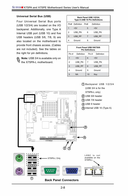
Backpanel USB 1/2/3/4
(USB 3/4 is for the
X7SPA-L only)
USB 5/6 header
USB 7/8 header
USB 9 header
Internal USB 10 (Type A)
Universal Serial Bus (USB)
Four Universal Serial Bus ports (USB 1/2/3/4) are located on the I/O backpanel. Additionally, one Type A Internal USB port (USB 10) and five USB headers (USB 5/6, 7/8, 9) are also located on the motherboard to provide front chassis access. (Cables are not included). See the tables on the right for pin definitions.
Note: USB 3/4 is available only on the X7SPA-L motherboard.
Back Panel USB 1/2/3/4,Type A USB 10 Pin Definitions
Pin# Definition Pin# Definition
1 +5V 5 +5V
2 USB_PN 6 USB_PN
3 USB_PP 7 USB_PP
4 Ground 8 Ground
Front Panel USB 5/6/7/8/9Pin Definitions
Pin # Definition Pin # Definition
1 +5V 6 +5V
2 USB_PN 7 USB_PN
3 USB_PP 8 USB_PP
4 Ground 9 Ground
5 NA 10 Key
4
3
1
2
5
1
2
MH
2
MH
3M
H4
D17
JPW1
JUSB
1
JD1
JPC3
JPUSB1
JWD
1
JPG1 JBMC1JPL1
JPT1
JPL2
JDIM
M2
1
JDIM
M1
JI2C
2
JI2C1JOH1JL1
JL2
SP1+
J2
J3
JBT1
JBAT1
JPCIE1
JUSB
5
JUSB4
JUSB3
JUSB
2
JLPC80
R105
0
JSMB1
FAN1 FAN2
JCO
M2
JCO
M4
JPI2C1
JWF1
J8
JVGA1
CD1
JPB
FAN
FAN
COMS CLEAR
2-3
DIS
ABL
E1-
2 EN
ABL
EJP
B:BM
C EN
ABL
E/D
ISA
BLE
CD-in
JPT1
:TPM
EN
ABL
E/D
ISA
BLE
1-2
ENA
BLE
2-3
DIS
ABL
E
AUDIO FP
T-SGPIO2 T-SGPIO1
JPI2
C:PW
R I2
C
JSMB1:SMBus1
JPU
SB1:
USB
WA
KE U
P
2-3
DIS
ABL
E1-
2 EN
ABL
E
JWF1
:DO
M P
WR
JD1:
1-3
PWR
LED
4-7
SPEA
KER
ON:ENABLEJI2C2OFF:DISABLE
JI2C1OFF:DISABLEON:ENABLE
JL2:
AUD
IO F
RON
T PA
NEL
SEL
ECT
ON
:AC'
97 F
RON
T PA
NEL
OFF
:HD
AU
DIO
FRO
NT
PAN
ELJP
G1:
VGA
2-3
DIS
ABL
E1-
2 EN
ABL
E2-
3 D
ISA
BLE
JPL2
:1-2
EN
ABL
E
JPL1
:1-2
EN
ABL
E2-
3 D
ISA
BLE
JL1:
CHA
SISS
INTR
USI
ON
JF1
PWR
ON
RST
X O
H/F
F N
IC2
NIC
1 H
DD
LED
PW
R LE
D X
NM
I
2-3
NM
IJW
D1:
1-2
RST
JBT1:
LAN2
LAN1
I-SATA5
I-SATA2
I-SATA4
I-SATA1
I-SATA3
I-SATA0
SLOT1 PCI-E X4 (IN X16 SLOT)
SYS
CPUKB/MOUSE
COM
4
COM
3
COM
2
COM1
SOD
IMM
2
SOD
IMM
1
CPU
J6J5
J10 J11
J12
J13
J14
JPF
Back Panel Connectors
4
3
5
2
X7SPA-L OnlyL A N 2 i s n o t available on the X7SPA-L

Chapter 2: Installation
2-9
Serial Ports
Two COM connections (COM1, COM2) are located on the motherboard. COM1 is located on the back I/O panel. COM2 is located just behind the back panel connectors to provide additional on-board serial connection support. See the table on the right for pin defini-tions.
Note: Additional COM3 and COM4 headers are available on the X7S-PA-L motherboard only.
Serial Ports-COM1/COM2/COM3/COM4Pin Definitions
Pin # Definition Pin # Definition
1 DCD 6 DSR
2 RXD 7 RTS
3 TXD 8 CTS
4 DTR 9 RI
5 Ground 10 N/A
(Backpanel) COM1
COM2
COM3 (X7SPA-L Only)
COM4 (X7SPA-L Only)
1
1
2MH
2
MH
3M
H4
D17
JPW1
JUSB
1
JD1
JPC3
JPUSB1
JWD
1
JPG1 JBMC1JPL1
JPT1
JPL2
JDIM
M2
1
JDIM
M1
JI2C
2
JI2C1JOH1JL1
JL2
SP1+
J2
J3
JBT1
JBAT1
JPCIE1
JUSB
5
JUSB4
JUSB3
JUSB
2
JLPC80
R105
0
JSMB1
FAN1 FAN2
JCO
M2
JCO
M4
JPI2C1
JWF1
J8
JVGA1
CD1
JPB
FAN
FAN
COMS CLEAR
2-3
DIS
ABL
E1-
2 EN
ABL
EJP
B:BM
C EN
ABL
E/D
ISA
BLE
CD-in
JPT1
:TPM
EN
ABL
E/D
ISA
BLE
1-2
ENA
BLE
2-3
DIS
ABL
E
AUDIO FP
T-SGPIO2 T-SGPIO1
JPI2
C:PW
R I2
C
JSMB1:SMBus1
JPU
SB1:
USB
WA
KE U
P
2-3
DIS
ABL
E1-
2 EN
ABL
E
JWF1
:DO
M P
WR
JD1:
1-3
PWR
LED
4-7
SPEA
KER
ON:ENABLEJI2C2OFF:DISABLE
JI2C1OFF:DISABLEON:ENABLE
JL2:
AUD
IO F
RON
T PA
NEL
SEL
ECT
ON
:AC'
97 F
RON
T PA
NEL
OFF
:HD
AU
DIO
FRO
NT
PAN
ELJP
G1:
VGA
2-3
DIS
ABL
E1-
2 EN
ABL
E2-
3 D
ISA
BLE
JPL2
:1-2
EN
ABL
E
JPL1
:1-2
EN
ABL
E2-
3 D
ISA
BLE
JL1:
CHA
SISS
INTR
USI
ON
JF1
PWR
ON
RST
X O
H/F
F N
IC2
NIC
1 H
DD
LED
PW
R LE
D X
NM
I
2-3
NM
IJW
D1:
1-2
RST
JBT1:
LAN2
LAN1
I-SATA5
I-SATA2
I-SATA4
I-SATA1
I-SATA3
I-SATA0
SLOT1 PCI-E X4 (IN X16 SLOT)
SYS
CPUKB/MOUSE
COM
4
COM
3
COM
2
COM1
SOD
IMM
2
SOD
IMM
1
CPU
J6J5
J10 J11
J12
J13
J14
JPF
Back Panel Connectors
432
4
3
X7SPA-L Only
L A N 2 i s n o t available on the X7SPA-L
2-10
X7SPA and X7SPE Motherboard Series User's Manual
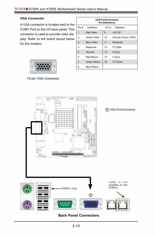
VGA Port/Connector1
VGA Connector
A VGA connector is located next to the COM1 Port on the I/O back panel. This connector is used to provide video dis-play. Refer to the board layout below for the location.
1
MH
2
MH
3M
H4
D17
JPW1
JUSB
1
JD1
JPC3
JPUSB1
JWD
1
JPG1 JBMC1JPL1
JPT1
JPL2
JDIM
M2
1
JDIM
M1
JI2C
2
JI2C1JOH1JL1
JL2
SP1+
J2
J3
JBT1
JBAT1
JPCIE1
JUSB
5
JUSB4
JUSB3
JUSB
2
JLPC80
R105
0
JSMB1
FAN1 FAN2
JCO
M2
JCO
M4
JPI2C1
JWF1
J8
JVGA1
CD1
JPB
FAN
FAN
COMS CLEAR
2-3
DIS
ABL
E1-
2 EN
ABL
EJP
B:BM
C EN
ABL
E/D
ISA
BLE
CD-in
JPT1
:TPM
EN
ABL
E/D
ISA
BLE
1-2
ENA
BLE
2-3
DIS
ABL
E
AUDIO FP
T-SGPIO2 T-SGPIO1
JPI2
C:PW
R I2
C
JSMB1:SMBus1
JPU
SB1:
USB
WA
KE U
P
2-3
DIS
ABL
E1-
2 EN
ABL
E
JWF1
:DO
M P
WR
JD1:
1-3
PWR
LED
4-7
SPEA
KER
ON:ENABLEJI2C2OFF:DISABLE
JI2C1OFF:DISABLEON:ENABLE
JL2:
AUD
IO F
RON
T PA
NEL
SEL
ECT
ON
:AC'
97 F
RON
T PA
NEL
OFF
:HD
AU
DIO
FRO
NT
PAN
ELJP
G1:
VGA
2-3
DIS
ABL
E1-
2 EN
ABL
E2-
3 D
ISA
BLE
JPL2
:1-2
EN
ABL
E
JPL1
:1-2
EN
ABL
E2-
3 D
ISA
BLE
JL1:
CHA
SISS
INTR
USI
ON
JF1
PWR
ON
RST
X O
H/F
F N
IC2
NIC
1 H
DD
LED
PW
R LE
D X
NM
I
2-3
NM
IJW
D1:
1-2
RST
JBT1:
LAN2
LAN1
I-SATA5
I-SATA2
I-SATA4
I-SATA1
I-SATA3
I-SATA0
SLOT1 PCI-E X4 (IN X16 SLOT)
SYS
CPUKB/MOUSE
COM
4
COM
3
COM
2
COM1
SOD
IMM
2
SOD
IMM
1
CPU
J6J5
J10 J11
J12
J13
J14
JPF
Back Panel Connectors
15-pin VGA Connector
VGA Port/ConnectorPin Definitions
Pin # Definition Pin # Definition
1 Red Video 9 +5V DC
2 Green Video 10 Ground (Vsync, DDC)
3 Blue Video 11 Reserved
4 Reserved 12 I2C Data
5 Ground 13 H Sync
6 Red Return 14 V Sync
7 Green Return 15 I2C Clock
8 Blue Return
X7SPA-L Only
L A N 2 i s n o t available on the X7SPA-L

Chapter 2: Installation
2-11
LAN1 (Shared w i th IPMI on the X7SPA-HF, X7SPE-HF, X7SPA-HF-D525 and X7SPE-HF-D525)
LAN2 (Not available on the X7SPA-L)
1
LAN Ports / IPMI
LAN ports are located on the I/O back panel. These ports accept RJ45 type cables. There are two Ethernet ports on the X7SPA-H, X7SPA-HF, X7SPE-H, X7SPE-HF, X7SPE-H-D525, X7SPE-HF-D525, X7SPA-H-D525, X7SPA-HF-D525 and one on the X7SPA-L motherboard
Note: IPMI on the X7SPA-HF, X7SPE-HF, X7SPE-HF-D525, X7SPA-HF-D525 is sup-ported through the same network connec-tion as LAN1.
Note: Please refer to the LED Indicator Section for LAN LED information.
1
2
2
MH
2
MH
3M
H4
D17
JPW1
JUSB
1
JD1
JPC3
JPUSB1
JWD
1
JPG1 JBMC1JPL1
JPT1
JPL2
JDIM
M2
1
JDIM
M1
JI2C
2
JI2C1JOH1JL1
JL2
SP1+
J2
J3
JBT1
JBAT1
JPCIE1
JUSB
5
JUSB4
JUSB3
JUSB
2
JLPC80
R105
0
JSMB1
FAN1 FAN2
JCO
M2
JCO
M4
JPI2C1
JWF1
J8
JVGA1
CD1
JPB
FAN
FAN
COMS CLEAR
2-3
DIS
ABL
E1-
2 EN
ABL
EJP
B:BM
C EN
ABL
E/D
ISA
BLE
CD-in
JPT1
:TPM
EN
ABL
E/D
ISA
BLE
1-2
ENA
BLE
2-3
DIS
ABL
E
AUDIO FP
T-SGPIO2 T-SGPIO1
JPI2
C:PW
R I2
C
JSMB1:SMBus1
JPU
SB1:
USB
WA
KE U
P
2-3
DIS
ABL
E1-
2 EN
ABL
E
JWF1
:DO
M P
WR
JD1:
1-3
PWR
LED
4-7
SPEA
KER
ON:ENABLEJI2C2OFF:DISABLE
JI2C1OFF:DISABLEON:ENABLE
JL2:
AUD
IO F
RON
T PA
NEL
SEL
ECT
ON
:AC'
97 F
RON
T PA
NEL
OFF
:HD
AU
DIO
FRO
NT
PAN
ELJP
G1:
VGA
2-3
DIS
ABL
E1-
2 EN
ABL
E2-
3 D
ISA
BLE
JPL2
:1-2
EN
ABL
E
JPL1
:1-2
EN
ABL
E2-
3 D
ISA
BLE
JL1:
CHA
SISS
INTR
USI
ON
JF1
PWR
ON
RST
X O
H/F
F N
IC2
NIC
1 H
DD
LED
PW
R LE
D X
NM
I
2-3
NM
IJW
D1:
1-2
RST
JBT1:
LAN2
LAN1
I-SATA5
I-SATA2
I-SATA4
I-SATA1
I-SATA3
I-SATA0
SLOT1 PCI-E X4 (IN X16 SLOT)
SYS
CPUKB/MOUSE
COM
4
COM
3
COM
2
COM1
SOD
IMM
2
SOD
IMM
1
CPU
J6J5
J10 J11
J12
J13
J14
JPF
Back Panel Connectors
RJ45/LANPin Definitions
Pin # Definition Pin # Definition
1 TX_D1+ 5 BI_D3-
2 TX_D1- 6 RX_D2-
3 RX_D2+ 7 BI_D4+
4 BI_D3+ 8 BI_D4-
L A N 2 i s n o t available on the X7SPA-L
Shared LAN1 / IPMI port (X7SPA-HF/X7SPE-HF/X7SPE-
HF-D525/X7SPA-HF-D525)
X7SPA-L Only

2-12
X7SPA and X7SPE Motherboard Series User's Manual
MH
2
MH
3M
H4
D17
JPW1
JUSB
1
JD1
JPC3
JPUSB1
JWD
1
JPG1 JBMC1JPL1
JPT1
JPL2
JDIM
M2
1
JDIM
M1
JI2C
2
JI2C1JOH1JL1
JL2
SP1+
J2
J3
JBT1
JBAT1
JPCIE1
JUSB
5
JUSB4
JUSB3
JUSB
2
JLPC80
R105
0JSMB1
FAN1 FAN2
JCO
M2
JCO
M4
JPI2C1
JWF1
J8
JVGA1
CD1
JPB
FAN
FAN
COMS CLEAR
2-3
DIS
ABL
E1-
2 EN
ABL
EJP
B:BM
C EN
ABL
E/D
ISA
BLE
CD-in
JPT1
:TPM
EN
ABL
E/D
ISA
BLE
1-2
ENA
BLE
2-3
DIS
ABL
E
AUDIO FP
T-SGPIO2 T-SGPIO1
JPI2
C:PW
R I2
C
JSMB1:SMBus1
JPU
SB1:
USB
WA
KE U
P
2-3
DIS
ABL
E1-
2 EN
ABL
E
JWF1
:DO
M P
WR
JD1:
1-3
PWR
LED
4-7
SPEA
KER
ON:ENABLEJI2C2OFF:DISABLE
JI2C1OFF:DISABLEON:ENABLE
JL2:
AUD
IO F
RON
T PA
NEL
SEL
ECT
ON
:AC'
97 F
RON
T PA
NEL
OFF
:HD
AU
DIO
FRO
NT
PAN
ELJP
G1:
VGA
2-3
DIS
ABL
E1-
2 EN
ABL
E2-
3 D
ISA
BLE
JPL2
:1-2
EN
ABL
E
JPL1
:1-2
EN
ABL
E2-
3 D
ISA
BLE
JL1:
CHA
SISS
INTR
USI
ON
JF1
PWR
ON
RST
X O
H/F
F N
IC2
NIC
1 H
DD
LED
PW
R LE
D X
NM
I
2-3
NM
IJW
D1:
1-2
RST
JBT1:
LAN2
LAN1
I-SATA5
I-SATA2
I-SATA4
I-SATA1
I-SATA3
I-SATA0
SLOT1 PCI-E X4 (IN X16 SLOT)
SYS
CPUKB/MOUSE
COM
4
COM
3
COM
2
COM1
SOD
IMM
2
SOD
IMM
1
CPU
J6J5
J10 J11
J12
J13
J14
JPF
Front Control PanelJF1 contains header pins for various buttons and indicators that are normally lo-cated on a control panel at the front of the chassis. These connectors are designed specifically for use with Supermicro server chassis. See the figure below for the descriptions of the various control panel buttons and LED indicators. Refer to the following section for descriptions and pin definitions.
JF1 Header Pins
Power Button
OH/Fan Fail LED
1
NIC1 LED
Reset Button
2
HDD LED
Power LEDVcc
Vcc
Vcc
Vcc
Ground
Ground
19 20
Vcc
X
GroundNMI
X
Vcc NIC2 LED
Power Fail LED
Pin 19 Pin 20
Pin 1 Pin 2

Chapter 2: Installation
2-13
Power Button
OH/Fan Fail LED
1
NIC1 LED
Reset Button
2
HDD LED
Power LEDVcc
Vcc
Vcc
Vcc
Ground
Ground
19 20
Vcc
X
GroundNMI
X
Vcc NIC2 LED
Power Fail LED
MH
2
MH
3M
H4
D17
JPW1
JUSB
1
JD1
JPC3
JPUSB1
JWD
1
JPG1 JBMC1JPL1
JPT1
JPL2
JDIM
M2
1
JDIM
M1
JI2C
2
JI2C1JOH1JL1
JL2
SP1+
J2
J3
JBT1
JBAT1
JPCIE1
JUSB
5
JUSB4
JUSB3
JUSB
2
JLPC80
R105
0
JSMB1
FAN1 FAN2
JCO
M2
JCO
M4
JPI2C1
JWF1
J8
JVGA1
CD1
JPB
FAN
FAN
COMS CLEAR
2-3
DIS
ABL
E1-
2 EN
ABL
EJP
B:BM
C EN
ABL
E/D
ISA
BLE
CD-in
JPT1
:TPM
EN
ABL
E/D
ISA
BLE
1-2
ENA
BLE
2-3
DIS
ABL
E
AUDIO FP
T-SGPIO2 T-SGPIO1
JPI2
C:PW
R I2
C
JSMB1:SMBus1
JPU
SB1:
USB
WA
KE U
P
2-3
DIS
ABL
E1-
2 EN
ABL
E
JWF1
:DO
M P
WR
JD1:
1-3
PWR
LED
4-7
SPEA
KER
ON:ENABLEJI2C2OFF:DISABLE
JI2C1OFF:DISABLEON:ENABLE
JL2:
AUD
IO F
RON
T PA
NEL
SEL
ECT
ON
:AC'
97 F
RON
T PA
NEL
OFF
:HD
AU
DIO
FRO
NT
PAN
ELJP
G1:
VGA
2-3
DIS
ABL
E1-
2 EN
ABL
E2-
3 D
ISA
BLE
JPL2
:1-2
EN
ABL
E
JPL1
:1-2
EN
ABL
E2-
3 D
ISA
BLE
JL1:
CHA
SISS
INTR
USI
ON
JF1
PWR
ON
RST
X O
H/F
F N
IC2
NIC
1 H
DD
LED
PW
R LE
D X
NM
I
2-3
NM
IJW
D1:
1-2
RST
JBT1:
LAN2
LAN1
I-SATA5
I-SATA2
I-SATA4
I-SATA1
I-SATA3
I-SATA0
SLOT1 PCI-E X4 (IN X16 SLOT)
SYS
CPUKB/MOUSE
COM
4
COM
3
COM
2
COM1
SOD
IMM
2
SOD
IMM
1
CPU
J6J5
J10 J11
J12
J13
J14
JPF
Front Control Panel Pin Definitions
Power LED
The Power LED connection is located on pins 15 and 16 of JF1. Refer to the table on the right for pin definitions.
Power LEDPin Definitions (JF1)
Pin# Definition
15 +3.3V
16 Ground
POWER LED
HDD LED
NIC1
NIC2
A
BA
HDD LED
The HDD LED connection is located on pins 13 and 14 of JF1. Attach a hard drive LED cable here to display disk activity (for any hard drive ac-tivities on the system, including Serial ATA and IDE). See the table on the right for pin definitions.
HDD LEDPin Definitions (JF1)
Pin# Definition
13 +3.3V
14 HD Active
B
JF1 Header Pins
NIC1/NIC2 LED Indicators
The NIC (Network Interface Controller or Ethernet Controller) LED connec-tion for LAN port 1 is located on pins 11 and 12 of JF1, and the LED con-nection for LAN Port 2 is on Pins 9 and 10. Attach the NIC LED cables to display network activity. Refer to the table on the right for pin definitions.
NIC 1/2 LEDPin Definitions (JF1)
Pin# Definition
11/9 Vcc
12/10 Ground
CD
CD

2-14
X7SPA and X7SPE Motherboard Series User's Manual
MH
2
MH
3M
H4
D17
JPW1
JUSB
1
JD1
JPC3
JPUSB1
JWD
1
JPG1 JBMC1JPL1
JPT1
JPL2
JDIM
M2
1
JDIM
M1
JI2C
2
JI2C1JOH1JL1
JL2
SP1+
J2
J3
JBT1
JBAT1
JPCIE1
JUSB
5
JUSB4
JUSB3
JUSB
2
JLPC80
R105
0
JSMB1
FAN1 FAN2
JCO
M2
JCO
M4
JPI2C1
JWF1
J8
JVGA1
CD1
JPB
FAN
FAN
COMS CLEAR
2-3
DIS
ABL
E1-
2 EN
ABL
EJP
B:BM
C EN
ABL
E/D
ISA
BLE
CD-in
JPT1
:TPM
EN
ABL
E/D
ISA
BLE
1-2
ENA
BLE
2-3
DIS
ABL
E
AUDIO FP
T-SGPIO2 T-SGPIO1
JPI2
C:PW
R I2
C
JSMB1:SMBus1
JPU
SB1:
USB
WA
KE U
P
2-3
DIS
ABL
E1-
2 EN
ABL
E
JWF1
:DO
M P
WR
JD1:
1-3
PWR
LED
4-7
SPEA
KER
ON:ENABLEJI2C2OFF:DISABLE
JI2C1OFF:DISABLEON:ENABLE
JL2:
AUD
IO F
RON
T PA
NEL
SEL
ECT
ON
:AC'
97 F
RON
T PA
NEL
OFF
:HD
AU
DIO
FRO
NT
PAN
ELJP
G1:
VGA
2-3
DIS
ABL
E1-
2 EN
ABL
E2-
3 D
ISA
BLE
JPL2
:1-2
EN
ABL
E
JPL1
:1-2
EN
ABL
E2-
3 D
ISA
BLE
JL1:
CHA
SISS
INTR
USI
ON
JF1
PWR
ON
RST
X O
H/F
F N
IC2
NIC
1 H
DD
LED
PW
R LE
D X
NM
I
2-3
NM
IJW
D1:
1-2
RST
JBT1:
LAN2
LAN1
I-SATA5
I-SATA2
I-SATA4
I-SATA1
I-SATA3
I-SATA0
SLOT1 PCI-E X4 (IN X16 SLOT)
SYS
CPUKB/MOUSE
COM
4
COM
3
COM
2
COM1
SOD
IMM
2
SOD
IMM
1
CPU
J6J5
J10 J11
J12
J13
J14
JPF
Power Button
OH/Fan Fail LED
1
NIC1 LED
Reset Button
2
HDD LED
Power LEDVcc
Vcc
Vcc
Vcc
Ground
Ground
19 20
Vcc
X
GroundNMI
X
Vcc NIC2 LED
Power Fail LED
OH/Fan Fail LED
Power Fail LED
Overheat (OH)/Fan Fail LED
Connect an LED Cable to the OH/Fan Fail connection on pins 7 and 8 of JF1 to provide advanced warnings of chassis overheat or fan failure. Refer to the table on the right for pin definitions.
OH/Fan Fail LEDPin Definitions (JF1)
Pin# Definition
7 Vcc
8 Ground
OH/Fan Fail Indicator Status
State Definition
Off Normal
On Overheat
Flash-ing
Fan Fail
A
B
JF1 Header Pins
AB
Power Fail LED
The Power Fail LED connection is located on pins 5 and 6 of JF1. Refer to the table on the right for pin defini-tions.
PWR Fail LEDPin Definitions (JF1)
Pin# Definition
5 Vcc
6 Ground

Chapter 2: Installation
2-15
MH
2
MH
3M
H4
D17
JPW1
JUSB
1
JD1
JPC3
JPUSB1
JWD
1
JPG1 JBMC1JPL1
JPT1
JPL2
JDIM
M2
1
JDIM
M1
JI2C
2
JI2C1JOH1JL1
JL2
SP1+
J2
J3
JBT1
JBAT1
JPCIE1
JUSB
5
JUSB4
JUSB3
JUSB
2
JLPC80
R105
0
JSMB1
FAN1 FAN2
JCO
M2
JCO
M4
JPI2C1
JWF1
J8
JVGA1
CD1
JPB
FAN
FAN
COMS CLEAR
2-3
DIS
ABL
E1-
2 EN
ABL
EJP
B:BM
C EN
ABL
E/D
ISA
BLE
CD-in
JPT1
:TPM
EN
ABL
E/D
ISA
BLE
1-2
ENA
BLE
2-3
DIS
ABL
E
AUDIO FP
T-SGPIO2 T-SGPIO1
JPI2
C:PW
R I2
C
JSMB1:SMBus1
JPU
SB1:
USB
WA
KE U
P
2-3
DIS
ABL
E1-
2 EN
ABL
E
JWF1
:DO
M P
WR
JD1:
1-3
PWR
LED
4-7
SPEA
KER
ON:ENABLEJI2C2OFF:DISABLE
JI2C1OFF:DISABLEON:ENABLE
JL2:
AUD
IO F
RON
T PA
NEL
SEL
ECT
ON
:AC'
97 F
RON
T PA
NEL
OFF
:HD
AU
DIO
FRO
NT
PAN
ELJP
G1:
VGA
2-3
DIS
ABL
E1-
2 EN
ABL
E2-
3 D
ISA
BLE
JPL2
:1-2
EN
ABL
E
JPL1
:1-2
EN
ABL
E2-
3 D
ISA
BLE
JL1:
CHA
SISS
INTR
USI
ON
JF1
PWR
ON
RST
X O
H/F
F N
IC2
NIC
1 H
DD
LED
PW
R LE
D X
NM
I
2-3
NM
IJW
D1:
1-2
RST
JBT1:
LAN2
LAN1
I-SATA5
I-SATA2
I-SATA4
I-SATA1
I-SATA3
I-SATA0
SLOT1 PCI-E X4 (IN X16 SLOT)
SYS
CPUKB/MOUSE
COM
4
COM
3
COM
2
COM1
SOD
IMM
2
SOD
IMM
1
CPU
J6J5
J10 J11
J12
J13
J14
JPF
Power Button
The Power Button connection is located on pins 1 and 2 of JF1. Momentarily contacting both pins will power on/off the system. To turn off the power when set to suspend mode, press the button for at least 4 seconds. Refer to the table on the right for pin definitions.
Power ButtonPin Definitions (JF1)
Pin# Definition
1 Signal
2 Ground
Reset Button
The Reset Button connection is located on pins 3 and 4 of JF1. Attach it to a hardware reset switch on the computer case. Refer to the table on the right for pin definitions.
Reset ButtonPin Definitions (JF1)
Pin# Definition
3 Reset
4 Ground
Reset Button
PWR Button
NMI Button
Power Button
OH/Fan Fail LED
1
NIC1 LED
Reset Button
2
HDD LED
Power LEDVcc
Vcc
Vcc
Vcc
Ground
Ground
19 20
Vcc
X
GroundNMI
X
Vcc NIC2 LED
Power Fail LED
AB
JF1 Header Pins
A
BC
C
NMI Button
The non-maskable interrupt button head-er is located on pins 19 and 20 of JF1. Refer to the table on the right for pin definitions.
NMI ButtonPin Definitions (JF1)
Pin# Definition
1 Signal
2 Ground

2-16
X7SPA and X7SPE Motherboard Series User's Manual
2-5 Connecting Cables
This section provides brief descriptions and pin-out definitions for onboard power connectors. Be sure to use the correct cable for each header or connector.
24-pin ATX Main PWR
4-pin External PWR A
B
ATX Power 24-pin ConnectorPin Definitions (JPW1)
Pin# Definition Pin # Definition
13 +3.3V 1 +3.3V
14 -12V 2 +3.3V
15 COM 3 COM
16 PS_ON 4 +5V
17 COM 5 COM
18 COM 6 +5V
19 COM 7 COM
20 Res (NC) 8 PWR_OK
21 +5V 9 5VSB
22 +5V 10 +12V
23 +5V 11 +12V
24 COM 12 +3.3V
(Optional)
(Required)
ATX Main PWR & CPU PWR Connectors
The 24-pin main power connector (JPW1) is used to provide power to the motherboard. This connector meets the SSI EPS 12V specification. See the table on the right for pin definitions.
MH
2
MH
3M
H4
D17
JPW1
JUSB
1
JD1
JPC3
JPUSB1
JWD
1
JPG1 JBMC1JPL1
JPT1
JPL2
JDIM
M2
1
JDIM
M1
JI2C
2
JI2C1JOH1JL1
JL2
SP1+
J2
J3
JBT1
JBAT1
JPCIE1
JUSB
5
JUSB4
JUSB3
JUSB
2
JLPC80
R105
0
JSMB1
FAN1 FAN2
JCO
M2
JCO
M4
JPI2C1
JWF1
J8
JVGA1
CD1
JPB
FAN
FAN
COMS CLEAR
2-3
DIS
ABL
E1-
2 EN
ABL
EJP
B:BM
C EN
ABL
E/D
ISA
BLE
CD-in
JPT1
:TPM
EN
ABL
E/D
ISA
BLE
1-2
ENA
BLE
2-3
DIS
ABL
E
AUDIO FP
T-SGPIO2 T-SGPIO1
JPI2
C:PW
R I2
C
JSMB1:SMBus1
JPU
SB1:
USB
WA
KE U
P
2-3
DIS
ABL
E1-
2 EN
ABL
E
JWF1
:DO
M P
WR
JD1:
1-3
PWR
LED
4-7
SPEA
KER
ON:ENABLEJI2C2OFF:DISABLE
JI2C1OFF:DISABLEON:ENABLE
JL2:
AUD
IO F
RON
T PA
NEL
SEL
ECT
ON
:AC'
97 F
RON
T PA
NEL
OFF
:HD
AU
DIO
FRO
NT
PAN
ELJP
G1:
VGA
2-3
DIS
ABL
E1-
2 EN
ABL
E2-
3 D
ISA
BLE
JPL2
:1-2
EN
ABL
E
JPL1
:1-2
EN
ABL
E2-
3 D
ISA
BLE
JL1:
CHA
SISS
INTR
USI
ON
JF1
PWR
ON
RST
X O
H/F
F N
IC2
NIC
1 H
DD
LED
PW
R LE
D X
NM
I
2-3
NM
IJW
D1:
1-2
RST
JBT1:
LAN2
LAN1
I-SATA5
I-SATA2
I-SATA4
I-SATA1
I-SATA3
I-SATA0
SLOT1 PCI-E X4 (IN X16 SLOT)
SYS
CPUKB/MOUSE
COM
4
COM
3
COM
2
COM1
SOD
IMM
2
SOD
IMM
1
CPU
J6J5
J10 J11
J12
J13
J14
JPF
B
A
External Power Connector
In addition to the 24-pin main power con-nector and 4-pin CPU power connectors, the 4-pin External Power connector at J8 is used to provide power to external devices such as hard disks & CD-ROM drives. This power connector supports 12V and 5V devices.
4-Pin External Power Connector
Pin Definitions
Pin Definition
1 +12V
2 Ground 1
3 Ground 2
4 +5V
Do NOT connect the power supply to this connector. Its purpose is to supply power to devices such as CD drives, hard drives and similar devices, it's not meant to receive power from the power supply.

Chapter 2: Installation
2-17
MH
2
MH
3M
H4
D17
JPW1
JUSB
1
JD1
JPC3
JPUSB1
JWD
1
JPG1 JBMC1JPL1
JPT1
JPL2
JDIM
M2
1
JDIM
M1
JI2C
2
JI2C1JOH1JL1
JL2
SP1+
J2
J3
JBT1
JBAT1
JPCIE1
JUSB
5
JUSB4
JUSB3
JUSB
2
JLPC80
R105
0
JSMB1
FAN1 FAN2
JCO
M2
JCO
M4
JPI2C1
JWF1
J8
JVGA1
CD1
JPB
FAN
FAN
COMS CLEAR
2-3
DIS
ABL
E1-
2 EN
ABL
EJP
B:BM
C EN
ABL
E/D
ISA
BLE
CD-in
JPT1
:TPM
EN
ABL
E/D
ISA
BLE
1-2
ENA
BLE
2-3
DIS
ABL
E
AUDIO FP
T-SGPIO2 T-SGPIO1
JPI2
C:PW
R I2
C
JSMB1:SMBus1
JPU
SB1:
USB
WA
KE U
P
2-3
DIS
ABL
E1-
2 EN
ABL
E
JWF1
:DO
M P
WR
JD1:
1-3
PWR
LED
4-7
SPEA
KER
ON:ENABLEJI2C2OFF:DISABLE
JI2C1OFF:DISABLEON:ENABLE
JL2:
AUD
IO F
RON
T PA
NEL
SEL
ECT
ON
:AC'
97 F
RON
T PA
NEL
OFF
:HD
AU
DIO
FRO
NT
PAN
ELJP
G1:
VGA
2-3
DIS
ABL
E1-
2 EN
ABL
E2-
3 D
ISA
BLE
JPL2
:1-2
EN
ABL
E
JPL1
:1-2
EN
ABL
E2-
3 D
ISA
BLE
JL1:
CHA
SISS
INTR
USI
ON
JF1
PWR
ON
RST
X O
H/F
F N
IC2
NIC
1 H
DD
LED
PW
R LE
D X
NM
I
2-3
NM
IJW
D1:
1-2
RST
JBT1:
LAN2
LAN1
I-SATA5
I-SATA2
I-SATA4
I-SATA1
I-SATA3
I-SATA0
SLOT1 PCI-E X4 (IN X16 SLOT)
SYS
CPUKB/MOUSE
COM
4
COM
3
COM
2
COM1
SOD
IMM
2
SOD
IMM
1
CPU
J6J5
J10 J11
J12
J13
J14
JPF
Fan HeaderPin Definitions
Pin# Definition
1 Ground
2 +12V
3 Tachometer
4 PWM_Control
Fan Headers
The X7SPA and X7SPE series has two fan headers. Fan1 is the CPU fan and Fan2 is for the system cooling fan. These fans are 4-pin fan headers. However, Pins 1~3 of the fan headers are backward compat-ible with the traditional 3-pin fans. (Note: Please use all 3-pin fans or all 4-pin fans on a motherboard. Please do not use 3-pin fans and 4-pin fans on the same board. Refer to the table on the right for pin definitions.
Note: The speeds of 4-pin (PWM) fans are controlled by Thermal Man-agement via BIOS Hardware Moni-toring in the Advanced Setting. (The default setting is Disabled.)
A B
Fan1 (CPU)
Fan2AB
2-18
X7SPA and X7SPE Motherboard Series User's Manual
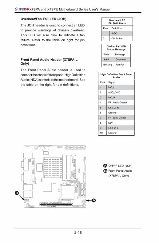
Overheat/Fan Fail LED (JOH)
The JOH header is used to connect an LED to provide warnings of chassis overheat. This LED will also blink to indicate a fan failure. Refer to the table on right for pin definitions.
Overheat LEDPin Definitions
Pin# Definition
1 5vDC
2 OH Active
OH/Fan Fail LEDStatus Message
State Message
Solid Overheat
Blinking Fan Fail
MH
2
MH
3M
H4
D17
JPW1
JUSB
1
JD1
JPC3
JPUSB1
JWD
1
JPG1 JBMC1JPL1
JPT1
JPL2
JDIM
M2
1
JDIM
M1
JI2C
2
JI2C1JOH1JL1
JL2
SP1+
J2
J3
JBT1
JBAT1
JPCIE1
JUSB
5
JUSB4
JUSB3
JUSB
2
JLPC80
R105
0
JSMB1
FAN1 FAN2
JCO
M2
JCO
M4
JPI2C1
JWF1
J8
JVGA1
CD1
JPB
FAN
FAN
COMS CLEAR
2-3
DIS
ABL
E1-
2 EN
ABL
EJP
B:BM
C EN
ABL
E/D
ISA
BLE
CD-in
JPT1
:TPM
EN
ABL
E/D
ISA
BLE
1-2
ENA
BLE
2-3
DIS
ABL
E
AUDIO FP
T-SGPIO2 T-SGPIO1
JPI2
C:PW
R I2
C
JSMB1:SMBus1
JPU
SB1:
USB
WA
KE U
P
2-3
DIS
ABL
E1-
2 EN
ABL
E
JWF1
:DO
M P
WR
JD1:
1-3
PWR
LED
4-7
SPEA
KER
ON:ENABLEJI2C2OFF:DISABLE
JI2C1OFF:DISABLEON:ENABLE
JL2:
AUD
IO F
RON
T PA
NEL
SEL
ECT
ON
:AC'
97 F
RON
T PA
NEL
OFF
:HD
AU
DIO
FRO
NT
PAN
ELJP
G1:
VGA
2-3
DIS
ABL
E1-
2 EN
ABL
E2-
3 D
ISA
BLE
JPL2
:1-2
EN
ABL
E
JPL1
:1-2
EN
ABL
E2-
3 D
ISA
BLE
JL1:
CHA
SISS
INTR
USI
ON
JF1
PWR
ON
RST
X O
H/F
F N
IC2
NIC
1 H
DD
LED
PW
R LE
D X
NM
I
2-3
NM
IJW
D1:
1-2
RST
JBT1:
LAN2
LAN1
I-SATA5
I-SATA2
I-SATA4
I-SATA1
I-SATA3
I-SATA0
SLOT1 PCI-E X4 (IN X16 SLOT)
SYS
CPUKB/MOUSE
COM
4
COM
3
COM
2
COM1
SOD
IMM
2
SOD
IMM
1
CPU
J6J5
J10 J11
J12
J13
J14
JPF
OH/FF LED (JOH)
Front Panel Audio
(X7SPA-L Only)
A
B
A
B
High Definition Front Panel Audio
Pin# Signal
1 MC_L
2 AUD_GND
3 MC_R
4 FP_Audio-Detect
5 Line_2_R
6 Ground
7 FP_Jack-Detect
8 Key
9 Line_2_L
10 Ground
Front Panel Audio Header (X7SPA-L Only)
The Front Panel Audio header is used to connect the chassis' front panel High Definition Audio (HDA) controls to the motherboard. See the table on the right for pin definitions.

Chapter 2: Installation
2-19
MH
2
MH
3M
H4
D17
JPW1
JUSB
1
JD1
JPC3
JPUSB1
JWD
1
JPG1 JBMC1JPL1
JPT1
JPL2
JDIM
M2
1
JDIM
M1
JI2C
2
JI2C1JOH1JL1
JL2
SP1+
J2
J3
JBT1
JBAT1
JPCIE1
JUSB
5
JUSB4
JUSB3
JUSB
2
JLPC80
R105
0
JSMB1
FAN1 FAN2
JCO
M2
JCO
M4
JPI2C1
JWF1
J8
JVGA1
CD1
JPB
FAN
FAN
COMS CLEAR
2-3
DIS
ABL
E1-
2 EN
ABL
EJP
B:BM
C EN
ABL
E/D
ISA
BLE
CD-in
JPT1
:TPM
EN
ABL
E/D
ISA
BLE
1-2
ENA
BLE
2-3
DIS
ABL
E
AUDIO FP
T-SGPIO2 T-SGPIO1
JPI2
C:PW
R I2
C
JSMB1:SMBus1
JPU
SB1:
USB
WA
KE U
P
2-3
DIS
ABL
E1-
2 EN
ABL
E
JWF1
:DO
M P
WR
JD1:
1-3
PWR
LED
4-7
SPEA
KER
ON:ENABLEJI2C2OFF:DISABLE
JI2C1OFF:DISABLEON:ENABLE
JL2:
AUD
IO F
RON
T PA
NEL
SEL
ECT
ON
:AC'
97 F
RON
T PA
NEL
OFF
:HD
AU
DIO
FRO
NT
PAN
ELJP
G1:
VGA
2-3
DIS
ABL
E1-
2 EN
ABL
E2-
3 D
ISA
BLE
JPL2
:1-2
EN
ABL
E
JPL1
:1-2
EN
ABL
E2-
3 D
ISA
BLE
JL1:
CHA
SISS
INTR
USI
ON
JF1
PWR
ON
RST
X O
H/F
F N
IC2
NIC
1 H
DD
LED
PW
R LE
D X
NM
I
2-3
NM
IJW
D1:
1-2
RST
JBT1:
LAN2
LAN1
I-SATA5
I-SATA2
I-SATA4
I-SATA1
I-SATA3
I-SATA0
SLOT1 PCI-E X4 (IN X16 SLOT)
SYS
CPUKB/MOUSE
COM
4
COM
3
COM
2
COM1
SOD
IMM
2
SOD
IMM
1
CPU
J6J5
J10 J11
J12
J13
J14
JPF
Chassis Intrusion
SATA DOM Power
I2C Connector
A
Chassis Intrusion
A Chassis Intrusion header is located at JL1 on the motherboard. Attach the appropriate cable from the chassis to inform you of a chassis intrusion when the chassis is opened.
Chassis IntrusionPin Definitions (JL1)
Pin# Definition
1 Intrusion Input
2 Ground
B
A
SATA DOM Power
The SATA DOM Power on JWF1 is used to supply power to SATA Disk-on-Module (DOM) solid-state storage devices.
B
Power SMB I2C Connector
Power System Management Bus (I2C) Connector monitors the status of the power supply, fan and system temperature. See the table on the right for pin definitions.
PWR Supply I2CPin Definitions
Pin# Definition
1 Clock
2 Data
3 PWR Fail
4 Ground
5 +3.3V
C
C

2-20
X7SPA and X7SPE Motherboard Series User's Manual
CD Header (X7SPA-L Only)
A 4-pin CD header located at CD1 is avail-able on the X7SPA-L. This header allows you to use the onboard sound for audio CD playback. Connect an audio cable from your CD drive to the header that fits your cable's connector. See the table at right for pin defi-nitions.
CD HeaderPin Definitions
Pin# Definition
1 Left Stereo Signal
2 Ground
3 Ground
4 Right Stereo Signal
MH
2
MH
3M
H4
D17
JPW1
JUSB
1
JD1
JPC3
JPUSB1
JWD
1
JPG1 JBMC1JPL1
JPT1
JPL2
JDIM
M2
1
JDIM
M1
JI2C
2
JI2C1JOH1JL1
JL2
SP1+
J2
J3
JBT1
JBAT1
JPCIE1
JUSB
5
JUSB4
JUSB3
JUSB
2
JLPC80
R105
0
JSMB1
FAN1 FAN2
JCO
M2
JCO
M4
JPI2C1
JWF1
J8
JVGA1
CD1
JPB
FAN
FAN
COMS CLEAR
2-3
DIS
ABL
E1-
2 EN
ABL
EJP
B:BM
C EN
ABL
E/D
ISA
BLE
CD-in
JPT1
:TPM
EN
ABL
E/D
ISA
BLE
1-2
ENA
BLE
2-3
DIS
ABL
E
AUDIO FP
T-SGPIO2 T-SGPIO1
JPI2
C:PW
R I2
C
JSMB1:SMBus1
JPU
SB1:
USB
WA
KE U
P
2-3
DIS
ABL
E1-
2 EN
ABL
E
JWF1
:DO
M P
WR
JD1:
1-3
PWR
LED
4-7
SPEA
KER
ON:ENABLEJI2C2OFF:DISABLE
JI2C1OFF:DISABLEON:ENABLE
JL2:
AUD
IO F
RON
T PA
NEL
SEL
ECT
ON
:AC'
97 F
RON
T PA
NEL
OFF
:HD
AU
DIO
FRO
NT
PAN
ELJP
G1:
VGA
2-3
DIS
ABL
E1-
2 EN
ABL
E2-
3 D
ISA
BLE
JPL2
:1-2
EN
ABL
E
JPL1
:1-2
EN
ABL
E2-
3 D
ISA
BLE
JL1:
CHA
SISS
INTR
USI
ON
JF1
PWR
ON
RST
X O
H/F
F N
IC2
NIC
1 H
DD
LED
PW
R LE
D X
NM
I
2-3
NM
IJW
D1:
1-2
RST
JBT1:
LAN2
LAN1
I-SATA5
I-SATA2
I-SATA4
I-SATA1
I-SATA3
I-SATA0
SLOT1 PCI-E X4 (IN X16 SLOT)
SYS
CPUKB/MOUSE
COM
4
COM
3
COM
2
COM1
SOD
IMM
2
SOD
IMM
1
CPU
J6J5
J10 J11
J12
J13
J14
JPF
CD Header
SMBr
T-SGPIO Headers
A
B
A
B
Serial_Link-SGPIOPin Definitions
Pin# Definition Pin Definition
1 NC 2 NC
3 Ground 4 DATA Out
5 Load 6 Ground
7 Clock 8 NC
T-SGPIO 0/1 Headers
Two T-SGPIO (Serial-Link General Pur-pose Input/Output) headers are located near the SATA connectors on the moth-erboard. These headers are used to communicate with the enclosure manage-ment chip in the system. See the table on the right for pin definitions. Refer to the board layout below for the locations of the headers. NC: No Connections
C
C
SMB
A System Management Bus (SMB) header is located at JSMB. Connect the appropriate cable here to use the SMB I2C connection on your system.
SMB HeaderPin Definition
Pin# Definition
1 Data
2 Ground
3 Clock
4 No Connection

Chapter 2: Installation
2-21
LVDS Connector (X7SPA-L Only)
An LVDS connector (J5) is available on the X7SPA-L only. This connector provides 18-bit LVDS (Low Voltage Differential Signaling) for an LCD panel or other similar devices. Refer to the table on the right for pin definitions.
MH
2
MH
3M
H4
D17
JPW1
JUSB
1
JD1
JPC3
JPUSB1
JWD
1
JPG1 JBMC1JPL1
JPT1
JPL2
JDIM
M2
1
JDIM
M1
JI2C
2
JI2C1JOH1JL1
JL2
SP1+
J2
J3
JBT1
JBAT1
JPCIE1
JUSB
5
JUSB4
JUSB3
JUSB
2
JLPC80
R105
0
JSMB1
FAN1 FAN2
JCO
M2
JCO
M4
JPI2C1
JWF1
J8
JVGA1
CD1
JPB
FAN
FAN
COMS CLEAR
2-3
DIS
ABL
E1-
2 EN
ABL
EJP
B:BM
C EN
ABL
E/D
ISA
BLE
CD-in
JPT1
:TPM
EN
ABL
E/D
ISA
BLE
1-2
ENA
BLE
2-3
DIS
ABL
E
AUDIO FP
T-SGPIO2 T-SGPIO1
JPI2
C:PW
R I2
C
JSMB1:SMBus1
JPU
SB1:
USB
WA
KE U
P
2-3
DIS
ABL
E1-
2 EN
ABL
E
JWF1
:DO
M P
WR
JD1:
1-3
PWR
LED
4-7
SPEA
KER
ON:ENABLEJI2C2OFF:DISABLE
JI2C1OFF:DISABLEON:ENABLE
JL2:
AUD
IO F
RON
T PA
NEL
SEL
ECT
ON
:AC'
97 F
RON
T PA
NEL
OFF
:HD
AU
DIO
FRO
NT
PAN
ELJP
G1:
VGA
2-3
DIS
ABL
E1-
2 EN
ABL
E2-
3 D
ISA
BLE
JPL2
:1-2
EN
ABL
E
JPL1
:1-2
EN
ABL
E2-
3 D
ISA
BLE
JL1:
CHA
SISS
INTR
USI
ON
JF1
PWR
ON
RST
X O
H/F
F N
IC2
NIC
1 H
DD
LED
PW
R LE
D X
NM
I
2-3
NM
IJW
D1:
1-2
RST
JBT1:
LAN2
LAN1
I-SATA5
I-SATA2
I-SATA4
I-SATA1
I-SATA3
I-SATA0
SLOT1 PCI-E X4 (IN X16 SLOT)
SYS
CPUKB/MOUSE
COM
4
COM
3
COM
2
COM1
SOD
IMM
2
SOD
IMM
1
CPU
J6J5
J10 J11
J12
J13
J14
JPF
LVDS Connector
Inverter Connector
A
B
B
LVDSPin Definitions
Pin# Definition Pin Definition
1 3.3V 11 3.3V
2 LDATAP0 12 LDATAN0
3 GND 13 GND
4 LDATAP1 14 LDATAN1
5 GND 15 GND
6 LDATAP2 16 LDATAN2
7 GND 17 GND
8 NC 18 NC
9 LVDDEN 19 NC
10 LCLKP 20 LCLKN
A
Inverter Power Connector (X7SPA-L Only)
The inverter connector on J6 is a 7-pin connector and is used in conjunction with the LVDS connector. Connect the backlight module of the LCD panel to this socket. This controls the backlight lamp, PWM control signals, and inverter power.. Inverter Power
Pin Definitions
Pin# Definition
1 12V
2 12V
3 GND
4 GND
5 3.3V
6 3.3V
7 GND
8 GND
9 BKLTEN
10 BKLTCTL

2-22
X7SPA and X7SPE Motherboard Series User's Manual
TPM Header (X7SPE-H-D525, X7SPE-HF-D525 Only)
This header is used to connect a Trusted Platform Module (TPM), available from a third-party vendor. A TPM is a secu-rity device that allows encryption and authentication of hard drives. It enables the motherboard to deny access if the TPM associated with the hard drive is not installed in the system. See the table on the right for pin definitions.
TPM HeaderA
Trusted Platform Module HeaderPin Definitions
Pin # Definition Pin # Definition
1 LCLK 2 GND
3 LFRAME 4 No Pin
5 LRESET 6 VCC5
7 LAD3 8 LAD2
9 VCC3 10 LAD1
11 LAD0 12 GND
13 RSV0 14 RSV1
15 SB3V 16 SERIRQ
17 GND 18 CLKRUN
19 LPCPD 20 RSV2
MH
2
MH
3M
H4
D17
JPW1
JUSB
1
JD1
JWD
1
JPG1 JBMC1JPL1
JPL2
JDIM
M2
1
JDIM
M1
JI2C
2
JI2C1JOH1JL1
SP1+
J2
J3
JBT1
JBAT1
JPCIE1
JUSB
5
JUSB4
JUSB3
JUSB
2
JLPC80
R105
0
JSMB1
FAN1 FAN2
JCO
M2
JPI2C1
JWF1
J8
JVGA1
JPB
FAN
FAN
COMS CLEAR
2-3
DIS
ABL
E1-
2 EN
ABL
EJP
B:BM
C EN
ABL
E/D
ISA
BLE
JPT1
:TPM
EN
ABL
E/D
ISA
BLE
1-2
ENA
BLE
2-3
DIS
ABL
E
T-SGPIO2 T-SGPIO1
JPI2
C:PW
R I2
C
JSMB1:SMBus1
JPU
SB1:
USB
WA
KE U
P
2-3
DIS
ABL
E1-
2 EN
ABL
E
JWF1
:DO
M P
WR
JD1:
1-3
PWR
LED
4-7
SPEA
KER
ON:ENABLEJI2C2OFF:DISABLE
JL2:
AUD
IO F
RON
T PA
NEL
SEL
ECT
ON
:AC'
97 F
RON
T PA
NEL
OFF
:HD
AU
DIO
FRO
NT
PAN
ELJP
G1:
VGA
2-3
DIS
ABL
E1-
2 EN
ABL
E2-
3 D
ISA
BLE
JPL2
:1-2
EN
ABL
E
JPL1
:1-2
EN
ABL
E2-
3 D
ISA
BLE
JL1:
CHA
SISS
INTR
USI
ON
JF1
PWR
ON
RST
X O
H/F
F N
IC2
NIC
1 H
DD
LED
PW
R LE
D X
NM
I
2-3
NM
IJW
D1:
1-2
RST
JBT1:
LAN2
LAN1
I-SATA5
I-SATA2
I-SATA4
I-SATA1
I-SATA3
I-SATA0
SYS
CPUKB/MOUSE
COM
2
COM1
SOD
IMM
2
SOD
IMM
1
CPU
JPF
A

Chapter 2: Installation
2-23
2-6 Jumper Settings
Explanation of Jumpers
To modify the operation of the motherboard, jumpers can be used to choose between optional settings. Jumpers create shorts between two pins to change the function of the connector. Pin 1 is identified with a square solder pad on the printed circuit board.
Note: On two pin jumpers, "Closed" means the jumper is on and "Open" means the jumper is off the pins.

2-24
X7SPA and X7SPE Motherboard Series User's Manual
A LAN Port 1 Enable
LAN Port 2 Enable
(X7SPA-H, X7SPA-HF, X7SPE-HF, X7SPE-H, X7SPA-H-D525, X7SPA-HF-D525, X7SPE-H-D525, X7SPE-HF-D525 only)
JI2C1/JI2C2
LAN Port Enable/Disable
JPL1/JPL2 enable or disable LAN Port 1/LAN Port 2 on the motherboard. See the table on the right for jumper set-tings. The default setting is enabled.
Note: LAN Port 2 is not available on the X7SPA-L.
GLAN EnableJumper Settings
Pin# Definition
1-2 Enabled (default)
2-3 Disabled
B
B A
MH
2
MH
3M
H4
D17
JPW1
JUSB
1
JD1
JPC3
JPUSB1
JWD
1
JPG1 JBMC1JPL1
JPT1
JPL2
JDIM
M2
1
JDIM
M1
JI2C
2
JI2C1JOH1JL1
JL2
SP1+
J2
J3
JBT1
JBAT1
JPCIE1
JUSB
5
JUSB4
JUSB3
JUSB
2
JLPC80
R105
0
JSMB1
FAN1 FAN2
JCO
M2
JCO
M4
JPI2C1
JWF1
J8
JVGA1
CD1
JPB
FAN
FAN
COMS CLEAR
2-3
DIS
ABL
E1-
2 EN
ABL
EJP
B:BM
C EN
ABL
E/D
ISA
BLE
CD-in
JPT1
:TPM
EN
ABL
E/D
ISA
BLE
1-2
ENA
BLE
2-3
DIS
ABL
E
AUDIO FP
T-SGPIO2 T-SGPIO1
JPI2
C:PW
R I2
C
JSMB1:SMBus1
JPU
SB1:
USB
WA
KE U
P
2-3
DIS
ABL
E1-
2 EN
ABL
E
JWF1
:DO
M P
WR
JD1:
1-3
PWR
LED
4-7
SPEA
KER
ON:ENABLEJI2C2OFF:DISABLE
JI2C1OFF:DISABLEON:ENABLE
JL2:
AUD
IO F
RON
T PA
NEL
SEL
ECT
ON
:AC'
97 F
RON
T PA
NEL
OFF
:HD
AU
DIO
FRO
NT
PAN
ELJP
G1:
VGA
2-3
DIS
ABL
E1-
2 EN
ABL
E2-
3 D
ISA
BLE
JPL2
:1-2
EN
ABL
E
JPL1
:1-2
EN
ABL
E2-
3 D
ISA
BLE
JL1:
CHA
SISS
INTR
USI
ON
JF1
PWR
ON
RST
X O
H/F
F N
IC2
NIC
1 H
DD
LED
PW
R LE
D X
NM
I
2-3
NM
IJW
D1:
1-2
RST
JBT1:
LAN2
LAN1
I-SATA5
I-SATA2
I-SATA4
I-SATA1
I-SATA3
I-SATA0
SLOT1 PCI-E X4 (IN X16 SLOT)
SYS
CPUKB/MOUSE
COM
4
COM
3
COM
2
COM1
SOD
IMM
2
SOD
IMM
1
CPU
J6J5
J10 J11
J12
J13
J14
JPF
SMB (I2C) Bus to PCI Slots
Jumpers JI2C1 and JI2C2 allow you to con-nect the System Management Bus (SMB) to PCI-E and PCI slots. The default setting is set to Disabled. See the table on the right for jumper settings.
I2C to PCI-SlotsJumper Settings
Jumper Definition
On Enabled
Off Disabled (Default)
C
C

Chapter 2: Installation
2-25
MH
2
MH
3M
H4
D17
JPW1
JUSB
1
JD1
JPC3
JPUSB1
JWD
1
JPG1 JBMC1JPL1
JPT1
JPL2
JDIM
M2
1
JDIM
M1
JI2C
2
JI2C1JOH1JL1
JL2
SP1+
J2
J3
JBT1
JBAT1
JPCIE1
JUSB
5
JUSB4
JUSB3
JUSB
2
JLPC80
R105
0
JSMB1
FAN1 FAN2
JCO
M2
JCO
M4
JPI2C1
JWF1
J8
JVGA1
CD1
JPB
FAN
FAN
COMS CLEAR
2-3
DIS
ABL
E1-
2 EN
ABL
EJP
B:BM
C EN
ABL
E/D
ISA
BLE
CD-in
JPT1
:TPM
EN
ABL
E/D
ISA
BLE
1-2
ENA
BLE
2-3
DIS
ABL
E
AUDIO FP
T-SGPIO2 T-SGPIO1
JPI2
C:PW
R I2
C
JSMB1:SMBus1
JPU
SB1:
USB
WA
KE U
P
2-3
DIS
ABL
E1-
2 EN
ABL
E
JWF1
:DO
M P
WR
JD1:
1-3
PWR
LED
4-7
SPEA
KER
ON:ENABLEJI2C2OFF:DISABLE
JI2C1OFF:DISABLEON:ENABLE
JL2:
AUD
IO F
RON
T PA
NEL
SEL
ECT
ON
:AC'
97 F
RON
T PA
NEL
OFF
:HD
AU
DIO
FRO
NT
PAN
ELJP
G1:
VGA
2-3
DIS
ABL
E1-
2 EN
ABL
E2-
3 D
ISA
BLE
JPL2
:1-2
EN
ABL
E
JPL1
:1-2
EN
ABL
E2-
3 D
ISA
BLE
JL1:
CHA
SISS
INTR
USI
ON
JF1
PWR
ON
RST
X O
H/F
F N
IC2
NIC
1 H
DD
LED
PW
R LE
D X
NM
I
2-3
NM
IJW
D1:
1-2
RST
JBT1:
LAN2
LAN1
I-SATA5
I-SATA2
I-SATA4
I-SATA1
I-SATA3
I-SATA0
SLOT1 PCI-E X4 (IN X16 SLOT)
SYS
CPUKB/MOUSE
COM
4
COM
3
COM
2
COM1
SOD
IMM
2
SOD
IMM
1
CPU
J6J5
J10 J11
J12
J13
J14
JPF
CMOS Clear
JBT1 is used to clear CMOS. Instead of pins, this "jumper" consists of contact pads to prevent accidental clearing of CMOS. To clear CMOS, use a metal object such as a small screwdriver to touch both pads at the same time to short the connection. Always remove the AC power cord from the system before clear-ing CMOS.
Important: For an ATX power sup-ply, you must completely shut down the system, remove the AC power cord and then short JBT1 to clear CMOS.
A
A CMOS Clear
MH2
MH3
MH4
D17
JPW1
JUSB
1
JD1
JPC3
JPUSB1
JWD
1
JPG1 JBMC1JPL1
JPT1
JPL2
JDIM
M2
1
JDIM
M1
JI2C2
JI2C1JOH1JL1
JL2
SP1+
J2
J3
JBT1
JBAT1
JPCIE1
JUSB
5
JUSB4
JUSB3JUSB
2
JLPC80
R105
0
JSMB1
FAN1 FAN2
JCO
M2
JCO
M4
JPI2C1
JWF1
J8
JVGA1CD
1
JPB
FAN
FAN
COMS CLEAR
2-3
DIS
ABLE
1-2
ENAB
LEJP
B:BM
C EN
ABLE
/DIS
ABLE
CD-in
JPT1
:TPM
ENA
BLE/
DIS
ABLE
1-2
ENAB
LE2-
3 D
ISAB
LE
AUDIO FP
T-SGPIO2 T-SGPIO1
JPI2
C:PW
R I2
C
JSMB1:SMBus1
JPUS
B1:U
SB W
AKE
UP
2-3
DIS
ABLE
1-2
ENAB
LE
JWF1
:DO
M P
WR
JD1:
1-3
PWR
LED
4-7
SPEA
KER
ON:ENABLEJI2C2OFF:DISABLE
JI2C1OFF:DISABLEON:ENABLE
JL2:
AUD
IO F
RONT
PAN
EL S
ELEC
TO
N:AC
'97
FRO
NT P
ANEL
OFF
:HD
AUD
IO F
RONT
PAN
ELJP
G1:V
GA
2-3
DIS
ABLE
1-2
ENAB
LE2-
3 D
ISAB
LEJP
L2:1
-2 E
NABL
E
JPL1
:1-2
ENA
BLE
2-3
DIS
ABLE
JL1:
CHAS
ISS
INTR
USIO
N
JF1
PWR
ON
RST
X O
H/FF
NIC
2 NI
C1 H
DD
LED
PW
R LE
D X
NM
I
2-3
NMI
JWD
1:1-
2 RS
T
JBT1:
LAN2
LAN1
I-SATA5
I-SATA2
I-SATA4
I-SATA1
I-SATA3
I-SATA0
SLOT1 PCI-E X4 (IN X16 SLOT)
SYS
CPUKB/MOUSE
COM
4
COM
3
COM
2
COM1
SODI
MM
2
SODI
MM
1
CPU
J6J5
J10 J11
J12
J13
J14
JPF
Metal contact pads
Motherboard

2-26
X7SPA and X7SPE Motherboard Series User's Manual
MH
2
MH
3M
H4
D17
JPW1
JUSB
1
JD1
JPC3
JPUSB1
JWD
1
JPG1 JBMC1JPL1
JPT1
JPL2
JDIM
M2
1
JDIM
M1
JI2C
2
JI2C1JOH1JL1
JL2
SP1+
J2
J3
JBT1
JBAT1
JPCIE1
JUSB
5
JUSB4
JUSB3
JUSB
2
JLPC80
R105
0
JSMB1
FAN1 FAN2
JCO
M2
JCO
M4
JPI2C1
JWF1
J8
JVGA1
CD1
JPB
FAN
FAN
COMS CLEAR
2-3
DIS
ABL
E1-
2 EN
ABL
EJP
B:BM
C EN
ABL
E/D
ISA
BLE
CD-in
JPT1
:TPM
EN
ABL
E/D
ISA
BLE
1-2
ENA
BLE
2-3
DIS
ABL
E
AUDIO FP
T-SGPIO2 T-SGPIO1
JPI2
C:PW
R I2
C
JSMB1:SMBus1
JPU
SB1:
USB
WA
KE U
P
2-3
DIS
ABL
E1-
2 EN
ABL
E
JWF1
:DO
M P
WR
JD1:
1-3
PWR
LED
4-7
SPEA
KER
ON:ENABLEJI2C2OFF:DISABLE
JI2C1OFF:DISABLEON:ENABLE
JL2:
AUD
IO F
RON
T PA
NEL
SEL
ECT
ON
:AC'
97 F
RON
T PA
NEL
OFF
:HD
AU
DIO
FRO
NT
PAN
ELJP
G1:
VGA
2-3
DIS
ABL
E1-
2 EN
ABL
E2-
3 D
ISA
BLE
JPL2
:1-2
EN
ABL
E
JPL1
:1-2
EN
ABL
E2-
3 D
ISA
BLE
JL1:
CHA
SISS
INTR
USI
ON
JF1
PWR
ON
RST
X O
H/F
F N
IC2
NIC
1 H
DD
LED
PW
R LE
D X
NM
I
2-3
NM
IJW
D1:
1-2
RST
JBT1:
LAN2
LAN1
I-SATA5
I-SATA2
I-SATA4
I-SATA1
I-SATA3
I-SATA0
SLOT1 PCI-E X4 (IN X16 SLOT)
SYS
CPUKB/MOUSE
COM
4
COM
3
COM
2
COM1
SOD
IMM
2
SOD
IMM
1
CPU
J6J5
J10 J11
J12
J13
J14
JPF
A USB Wake-up
A
USB Wake-Up (Not Available on the X7SPE-H-D525, X7SPA-H-D525, X7SPA-HF-D525 and X7SPE-HF-D525)
Use JPUSB jumper to enable the function of "System Waking-Up via USB devices". This jumper allows you to "wake-up" the system by pressing a key on the USB keyboard or by clicking the USB mouse of your system. The JPUSB jumper is used together with the USB Wake-Up function in the BIOS. Enable both the jumper and the BIOS setting to activate this function. See the table on the right for jumper settings and jumper connections.
Note: The default jumper setting is "Dis-abled". When the "USB Wake-Up" function is enabled, it will be active on all USB ports.
USB Wake-Up Jumper Settings
Jumper Setting Definition
Pins 1-2 Enabled
Pins 2-3 Disabled (Default)

Chapter 2: Installation
2-27
TPM Support Enable (Not available on X7SPA-H-D525, X7SPA-HF-D525, X7SPE-H-D525, X7SPE-HF-D525)
JPT1 allows the user to enable TPM (Trust-ed Platform Modules) support to enhance data integrity and system security. See the table on the right for jumper settings. The default setting is enabled.
TPM Support Enable Jumper Settings
Jumper Setting Definition
1-2 Enabled (Default)
2-3 Disabled
Watch Dog Enable/Disable
Watch Dog (JWD) is a system monitor that can reboot the system when a software ap-plication hangs. Close pins 1~2 to reset the system if an application hangs. Close pins 2~3 to generate a non-maskable interrupt signal for the application that hangs. See the table on the right for jumper settings. Watch Dog must also be enabled in the BIOS.
Watch Dog Jumper Settings (JWD)
Jumper Setting Definition
Pins 1-2 Reset (default)
Pins 2-3 NMI
Open Disabled
COM3 Redirection Select (OEM Option)
This is an OEM option for the X7SPA-H, X7SPA-HF, X7SPE-H, X7SPE-HF, X7SPE-H-D525, X7SPA-H-D525, X7SPA-HF-D525 and X7SPE-HF-D525 only.
COM3 Select (JPC3)
Jumper Setting Definition
Pins 1-2 RS232 (default)
Pins 2-3 TTL
Open Disabled
MH
2
MH
3M
H4
D17
JPW1
JUSB
1
JD1
JPC3
JPUSB1
JWD
1
JPG1 JBMC1JPL1
JPT1
JPL2
JDIM
M2
1
JDIM
M1
JI2C
2
JI2C1JOH1JL1
JL2
SP1+
J2
J3
JBT1
JBAT1
JPCIE1
JUSB
5
JUSB4
JUSB3
JUSB
2
JLPC80
R105
0
JSMB1
FAN1 FAN2
JCO
M2
JCO
M4
JPI2C1
JWF1
J8
JVGA1
CD1
JPB
FAN
FAN
COMS CLEAR
2-3
DIS
ABL
E1-
2 EN
ABL
EJP
B:BM
C EN
ABL
E/D
ISA
BLE
CD-in
JPT1
:TPM
EN
ABL
E/D
ISA
BLE
1-2
ENA
BLE
2-3
DIS
ABL
E
AUDIO FP
T-SGPIO2 T-SGPIO1
JPI2
C:PW
R I2
C
JSMB1:SMBus1
JPU
SB1:
USB
WA
KE U
P
2-3
DIS
ABL
E1-
2 EN
ABL
E
JWF1
:DO
M P
WR
JD1:
1-3
PWR
LED
4-7
SPEA
KER
ON:ENABLEJI2C2OFF:DISABLE
JI2C1OFF:DISABLEON:ENABLE
JL2:
AUD
IO F
RON
T PA
NEL
SEL
ECT
ON
:AC'
97 F
RON
T PA
NEL
OFF
:HD
AU
DIO
FRO
NT
PAN
ELJP
G1:
VGA
2-3
DIS
ABL
E1-
2 EN
ABL
E2-
3 D
ISA
BLE
JPL2
:1-2
EN
ABL
E
JPL1
:1-2
EN
ABL
E2-
3 D
ISA
BLE
JL1:
CHA
SISS
INTR
USI
ON
JF1
PWR
ON
RST
X O
H/F
F N
IC2
NIC
1 H
DD
LED
PW
R LE
D X
NM
I
2-3
NM
IJW
D1:
1-2
RST
JBT1:
LAN2
LAN1
I-SATA5
I-SATA2
I-SATA4
I-SATA1
I-SATA3
I-SATA0
SLOT1 PCI-E X4 (IN X16 SLOT)
SYS
CPUKB/MOUSE
COM
4
COM
3
COM
2
COM1
SOD
IMM
2
SOD
IMM
1
CPU
J6J5
J10 J11
J12
J13
J14
JPF
A
B
C
A TPM Enable
Watch Dog Enable
COM3 Redirect(OEM option for the X7SPA-H, X7SPA-HF, X7SPE-H, X7SPE-HF, X7SPA-H-D525, X 7 S PA - H F - D 5 2 5 , X7SPE-H-D525, and X 7 S P E - H F - D 5 2 5 only).
BC

2-28
X7SPA and X7SPE Motherboard Series User's Manual
Power LED/Speaker
On the JD1 header, pins 1~3 are used for a power LED and pins 4~7 are used for an external speaker. If you wish to use the onboard speaker, you should close pins 6-7 with a jumper. See the table on the right for speaker pin definitions.
Speaker ConnectorPin Definitions
Pin Setting Definition
Pins 6-7 Internal Speaker
Pins 4-7 External Speaker
BMC (X7SPA-HF, X7SPE-HF, X7SPE-HF-D525, X7SPA-H-D525, X7SPA-HF-D525 Only)
The JPB jumper is used to enable or disable the on-board Baseboard Man-agement Controller (BMC) and the on-board IPMI feature. This jumper is used together with the IPMI settings in the BIOS. The default position is pins 1 and 2 to enable BMC. See the table on the right for jumper settings.
BMCPin Definitions
Pin Setting Definition
Pins 1-2 Enabled (Default)
Pins 2-3 Disabled
MH
2
MH
3M
H4
D17
JPW1
JUSB
1
JD1
JPC3
JPUSB1
JWD
1
JPG1 JBMC1JPL1
JPT1
JPL2
JDIM
M2
1
JDIM
M1
JI2C
2
JI2C1JOH1JL1
JL2
SP1+
J2
J3
JBT1
JBAT1
JPCIE1
JUSB
5
JUSB4
JUSB3
JUSB
2
JLPC80
R105
0
JSMB1
FAN1 FAN2
JCO
M2
JCO
M4
JPI2C1
JWF1
J8
JVGA1
CD1
JPB
FAN
FAN
COMS CLEAR
2-3
DIS
ABL
E1-
2 EN
ABL
EJP
B:BM
C EN
ABL
E/D
ISA
BLE
CD-in
JPT1
:TPM
EN
ABL
E/D
ISA
BLE
1-2
ENA
BLE
2-3
DIS
ABL
E
AUDIO FP
T-SGPIO2 T-SGPIO1
JPI2
C:PW
R I2
C
JSMB1:SMBus1
JPU
SB1:
USB
WA
KE U
P
2-3
DIS
ABL
E1-
2 EN
ABL
E
JWF1
:DO
M P
WR
JD1:
1-3
PWR
LED
4-7
SPEA
KER
ON:ENABLEJI2C2OFF:DISABLE
JI2C1OFF:DISABLEON:ENABLE
JL2:
AUD
IO F
RON
T PA
NEL
SEL
ECT
ON
:AC'
97 F
RON
T PA
NEL
OFF
:HD
AU
DIO
FRO
NT
PAN
ELJP
G1:
VGA
2-3
DIS
ABL
E1-
2 EN
ABL
E2-
3 D
ISA
BLE
JPL2
:1-2
EN
ABL
E
JPL1
:1-2
EN
ABL
E2-
3 D
ISA
BLE
JL1:
CHA
SISS
INTR
USI
ON
JF1
PWR
ON
RST
X O
H/F
F N
IC2
NIC
1 H
DD
LED
PW
R LE
D X
NM
I
2-3
NM
IJW
D1:
1-2
RST
JBT1:
LAN2
LAN1
I-SATA5
I-SATA2
I-SATA4
I-SATA1
I-SATA3
I-SATA0
SLOT1 PCI-E X4 (IN X16 SLOT)
SYS
CPUKB/MOUSE
COM
4
COM
3
COM
2
COM1
SOD
IMM
2
SOD
IMM
1
CPU
J6J5
J10 J11
J12
J13
J14
JPF
A
B
A Power LED/Speaker
BMC EnableB

Chapter 2: Installation
2-29
VGA Enable (X7SPA-HF, X7SPE-HF, X7SPE-HF-D525, X7SPA-HF-D525 only)
JPG1 allows the user to enable or disable the onboard VGA adapter on the X7SPA-HF, X7SPE-HF, X7SPA-HF-D525 and X7SPE-HF-D525. The default setting is Enabled.
VGA EnableJumper Settings
Pin# Definition
1-2 Enabled (default)
2-3 Disabled
HDA/AC97 Select (X7SPA-L Only)
JL2 allows the user to select between High Definition Audio (HDA) or legacy AC97 audio. The default setting is HD Audio.
HDA/AC97Jumper Settings
Pin# 1-2 Definition
Open HD Audio (default)
Closed AC97
MH
2
MH
3M
H4
D17
JPW1
JUSB
1
JD1
JPC3
JPUSB1
JWD
1
JPG1 JBMC1JPL1
JPT1
JPL2
JDIM
M2
1
JDIM
M1
JI2C
2
JI2C1JOH1JL1
JL2
SP1+
J2
J3
JBT1
JBAT1
JPCIE1
JUSB
5
JUSB4
JUSB3
JUSB
2JLPC80
R105
0
JSMB1
FAN1 FAN2
JCO
M2
JCO
M4
JPI2C1
JWF1
J8
JVGA1
CD1
JPB
FAN
FAN
COMS CLEAR
2-3
DIS
ABL
E1-
2 EN
ABL
EJP
B:BM
C EN
ABL
E/D
ISA
BLE
CD-in
JPT1
:TPM
EN
ABL
E/D
ISA
BLE
1-2
ENA
BLE
2-3
DIS
ABL
E
AUDIO FP
T-SGPIO2 T-SGPIO1
JPI2
C:PW
R I2
C
JSMB1:SMBus1
JPU
SB1:
USB
WA
KE U
P
2-3
DIS
ABL
E1-
2 EN
ABL
E
JWF1
:DO
M P
WR
JD1:
1-3
PWR
LED
4-7
SPEA
KER
ON:ENABLEJI2C2OFF:DISABLE
JI2C1OFF:DISABLEON:ENABLE
JL2:
AUD
IO F
RON
T PA
NEL
SEL
ECT
ON
:AC'
97 F
RON
T PA
NEL
OFF
:HD
AU
DIO
FRO
NT
PAN
ELJP
G1:
VGA
2-3
DIS
ABL
E1-
2 EN
ABL
E2-
3 D
ISA
BLE
JPL2
:1-2
EN
ABL
E
JPL1
:1-2
EN
ABL
E2-
3 D
ISA
BLE
JL1:
CHA
SISS
INTR
USI
ON
JF1
PWR
ON
RST
X O
H/F
F N
IC2
NIC
1 H
DD
LED
PW
R LE
D X
NM
I
2-3
NM
IJW
D1:
1-2
RST
JBT1:
LAN2
LAN1
I-SATA5
I-SATA2
I-SATA4
I-SATA1
I-SATA3
I-SATA0
SLOT1 PCI-E X4 (IN X16 SLOT)
SYS
CPUKB/MOUSE
COM
4
COM
3
COM
2
COM1
SOD
IMM
2
SOD
IMM
1
CPU
J6J5
J10 J11
J12
J13
J14
JPF
A
B
A VGA Enable
HDA/AC97 SelectB

2-30
X7SPA and X7SPE Motherboard Series User's Manual
DCD / P5V Select
This is an OEM option for the X7SPA-H, X7SPA-HF, X7SPE-H, X7SPE-HF, X7SPE-H-D525, X7SPE-HF-D525, X7SPA-H-D525, and X7SPA-HF-D525 only.
MH
2
MH
3M
H4
D17
JPW1
JUSB
1
JD1
JPC3
JPUSB1
JWD
1
JPG1 JBMC1JPL1
JPT1
JPL2
JDIM
M2
1
JDIM
M1
JI2C
2
JI2C1JOH1JL1
JL2
SP1+
J2
J3
JBT1
JBAT1
JPCIE1
JUSB
5
JUSB4
JUSB3
JUSB
2
JLPC80
R105
0
JSMB1
FAN1 FAN2
JCO
M2
JCO
M4
JPI2C1
JWF1
J8
JVGA1
CD1
JPB
FAN
FAN
COMS CLEAR
2-3
DIS
ABL
E1-
2 EN
ABL
EJP
B:BM
C EN
ABL
E/D
ISA
BLE
CD-in
JPT1
:TPM
EN
ABL
E/D
ISA
BLE
1-2
ENA
BLE
2-3
DIS
ABL
E
AUDIO FP
T-SGPIO2 T-SGPIO1
JPI2
C:PW
R I2
C
JSMB1:SMBus1
JPU
SB1:
USB
WA
KE U
P
2-3
DIS
ABL
E1-
2 EN
ABL
E
JWF1
:DO
M P
WR
JD1:
1-3
PWR
LED
4-7
SPEA
KER
ON:ENABLEJI2C2OFF:DISABLE
JI2C1OFF:DISABLEON:ENABLE
JL2:
AUD
IO F
RON
T PA
NEL
SEL
ECT
ON
:AC'
97 F
RON
T PA
NEL
OFF
:HD
AU
DIO
FRO
NT
PAN
ELJP
G1:
VGA
2-3
DIS
ABL
E1-
2 EN
ABL
E2-
3 D
ISA
BLE
JPL2
:1-2
EN
ABL
E
JPL1
:1-2
EN
ABL
E2-
3 D
ISA
BLE
JL1:
CHA
SISS
INTR
USI
ON
JF1
PWR
ON
RST
X O
H/F
F N
IC2
NIC
1 H
DD
LED
PW
R LE
D X
NM
I
2-3
NM
IJW
D1:
1-2
RST
JBT1:
LAN2
LAN1
I-SATA5
I-SATA2
I-SATA4
I-SATA1
I-SATA3
I-SATA0
SLOT1 PCI-E X4 (IN X16 SLOT)
SYS
CPUKB/MOUSE
COM
4
COM
3
COM
2
COM1
SOD
IMM
2
SOD
IMM
1
CPU
J6J5
J10 J11
J12
J13
J14
JPF
AB
A Power Force On
DCD / P5V Select (COM1)
DCD / P5V Select (COM2)
DCD / P5V Select (COM3)
DCD / P5V Select (COM4)
B
Power Force On Enable/Disable
Jumper JPF allows you to enable (force on) or disable the Power Force On function. If enabled, the power will always stay on automatically. If this function is disabled (the normal setting), the user needs to press the power button to power on the system.
Power Force On Enable/Disable
Jumper Settings
Jumper Setting Definition
Open Normal
Closed Force On
DCD / P5V SelectJumper Settings
Jumper Setting Definition
Pins 1-2 DCD
Pins 2-3 P5V
CDE
C
D
E

Chapter 2: Installation
2-31
LAN Port LEDs
Two LAN ports are located on the I/O Backplane. Each Ethernet LAN port has two LEDs. The yellow Activity LED (right, see below) indicates activity, while the Link/Speed LED (left) may be green, amber or off to indicate the speed of the connection. See the tables at right for more information.
2-7 Onboard Indicators
LAN Port 1
LAN Port 2 (Not available on
the X7SPA-L)Rear View (when facing the rear side of the chassis)
Activity LEDLink/Speed LED
A B
MH
2
MH
3M
H4
D17
JPW1
JUSB
1
JD1
JPC3
JPUSB1
JWD
1
JPG1 JBMC1JPL1
JPT1
JPL2
JDIM
M2
1
JDIM
M1
JI2C
2
JI2C1JOH1JL1
JL2
SP1+
J2
J3
JBT1
JBAT1
JPCIE1
JUSB
5
JUSB4
JUSB3
JUSB
2
JLPC80
R105
0
JSMB1
FAN1 FAN2
JCO
M2
JCO
M4
JPI2C1
JWF1
J8
JVGA1
CD1
JPB
FAN
FAN
COMS CLEAR
2-3
DIS
ABL
E1-
2 EN
ABL
EJP
B:BM
C EN
ABL
E/D
ISA
BLE
CD-in
JPT1
:TPM
EN
ABL
E/D
ISA
BLE
1-2
ENA
BLE
2-3
DIS
ABL
E
AUDIO FP
T-SGPIO2 T-SGPIO1
JPI2
C:PW
R I2
C
JSMB1:SMBus1
JPU
SB1:
USB
WA
KE U
P
2-3
DIS
ABL
E1-
2 EN
ABL
E
JWF1
:DO
M P
WR
JD1:
1-3
PWR
LED
4-7
SPEA
KER
ON:ENABLEJI2C2OFF:DISABLE
JI2C1OFF:DISABLEON:ENABLE
JL2:
AUD
IO F
RON
T PA
NEL
SEL
ECT
ON
:AC'
97 F
RON
T PA
NEL
OFF
:HD
AU
DIO
FRO
NT
PAN
ELJP
G1:
VGA
2-3
DIS
ABL
E1-
2 EN
ABL
E2-
3 D
ISA
BLE
JPL2
:1-2
EN
ABL
E
JPL1
:1-2
EN
ABL
E2-
3 D
ISA
BLE
JL1:
CHA
SISS
INTR
USI
ON
JF1
PWR
ON
RST
X O
H/F
F N
IC2
NIC
1 H
DD
LED
PW
R LE
D X
NM
I
2-3
NM
IJW
D1:
1-2
RST
JBT1:
LAN2
LAN1
I-SATA5
I-SATA2
I-SATA4
I-SATA1
I-SATA3
I-SATA0
SLOT1 PCI-E X4 (IN X16 SLOT)
SYS
CPUKB/MOUSE
COM
4
COM
3
COM
2
COM1
SOD
IMM
2
SOD
IMM
1
CPU
J6J5
J10 J11
J12
J13
J14
JPF
Back Panel Connectors
AB
GLAN Activity LED Indicator
Color Definition
Yellow (Flashing) ConnectionActive
GLAN Link/Speed LED Indicator
LED Color Definition
Off No Connection or 10 Mbps
Green (On) 100 Mbps
Amber (On) 1 Gbps

2-32
X7SPA and X7SPE Motherboard Series User's Manual
MH
2
MH
3M
H4
D17
JPW1
JUSB
1
JD1
JPC3
JPUSB1
JWD
1
JPG1 JBMC1JPL1
JPT1
JPL2
JDIM
M2
1
JDIM
M1
JI2C
2
JI2C1JOH1JL1
JL2
SP1+
J2
J3
JBT1
JBAT1
JPCIE1
JUSB
5
JUSB4
JUSB3
JUSB
2
JLPC80
R105
0
JSMB1
FAN1 FAN2
JCO
M2
JCO
M4
JPI2C1
JWF1
J8
JVGA1
CD1
JPB
FAN
FAN
COMS CLEAR
2-3
DIS
ABL
E1-
2 EN
ABL
EJP
B:BM
C EN
ABL
E/D
ISA
BLE
CD-in
JPT1
:TPM
EN
ABL
E/D
ISA
BLE
1-2
ENA
BLE
2-3
DIS
ABL
E
AUDIO FP
T-SGPIO2 T-SGPIO1
JPI2
C:PW
R I2
C
JSMB1:SMBus1
JPU
SB1:
USB
WA
KE U
P
2-3
DIS
ABL
E1-
2 EN
ABL
E
JWF1
:DO
M P
WR
JD1:
1-3
PWR
LED
4-7
SPEA
KER
ON:ENABLEJI2C2OFF:DISABLE
JI2C1OFF:DISABLEON:ENABLE
JL2:
AUD
IO F
RON
T PA
NEL
SEL
ECT
ON
:AC'
97 F
RON
T PA
NEL
OFF
:HD
AU
DIO
FRO
NT
PAN
ELJP
G1:
VGA
2-3
DIS
ABL
E1-
2 EN
ABL
E2-
3 D
ISA
BLE
JPL2
:1-2
EN
ABL
E
JPL1
:1-2
EN
ABL
E2-
3 D
ISA
BLE
JL1:
CHA
SISS
INTR
USI
ON
JF1
PWR
ON
RST
X O
H/F
F N
IC2
NIC
1 H
DD
LED
PW
R LE
D X
NM
I
2-3
NM
IJW
D1:
1-2
RST
JBT1:
LAN2
LAN1
I-SATA5
I-SATA2
I-SATA4
I-SATA1
I-SATA3
I-SATA0
SLOT1 PCI-E X4 (IN X16 SLOT)
SYS
CPUKB/MOUSE
COM
4
COM
3
COM
2
COM1
SOD
IMM
2
SOD
IMM
1
CPU
J6J5
J10 J11
J12
J13
J14
JPF
2-8 Serial ATA and HDD Connections
Note the following conditions when connecting the Serial ATA and hard disk drive cables:
• Be sure to use the correct cable for each connector. Refer to Page 1-1 for cables that came with your shipment.
A
SATA Connectors
Six (6) Serial ATA (SATA) connectors (I-SATA 0~5) are located on the mother-board, to provide serial link connections. Serial Link connections provide faster data transmission than those of the tra-ditional Parallel ATA. These four SATA connectors are supported by the Intel ICH9/9R South Bridge. See the table on the right for pin definitions.
Note: There are Four (4) SATA ports on the X7SPA-L.
SATA Connectors Pin Definitions
Pin# Signal
1 Ground
2 SATA_TXP
3 SATA_TXN
4 Ground
5 SATA_RXN
6 SATA_RXP
7 Ground
BC
DE
F
I-SATA0
I-SATA1
I-SATA2*
I-SATA5*
I-SATA4
I-SATA3
ABCDEF
*I-SATA2 and I-SATA3 are not
available on the X7SPA-L.