x3-10m - fpga & data acquisition systems digital signal … · 2016-02-24 · system interface...
TRANSCRIPT

X3-10M
DESCRIPTIONThe X3-10M is an XMC IO module featuring eightsimultaneously sampling 16-bit, 25 MSPS A/D channelsdesigned for high speed instrumentation and analysis forneuro-physical, RADAR, and high speed data acquisitionapplications.
Flexible trigger methods include counted frames, softwaretriggering and external triggering. The sample rate clock iseither an external clock or on-board programmable PLL clocksource.
Data acquisition control, signal processing, buffering, andsystem interface functions are implemented in a XilinxSpartan3A DSP FPGA, 1.8M gate device. Two 512Kx32memory devices are used for data buffering and FPGAcomputing memory.
The logic can be fully customized using VHDL and MATLABusing the FrameWork Logic toolset. The MATLAB BSPsupports real-time hardware-in-the-loop development usingthe graphical, block diagram Simulink environment withXilinx System Generator.
The PCI Express interface supports continuous data rates upto 180 MB/ s between the module and the host. A flexibledata packet system implemented over the PCIe interfaceprovides both high data rates to the host that is readilyexpandable for custom applications.
FEATURES• 8 channels of 25 MSPS, 16-bit simultaneously
sampling A/D
• -110 dB noise floor, 97 dB SFDR
• Snap any channel pair at up to 20 MSPS per channel
• Continuously acquire 8 simultaneous channels at 10 MSPS to system memory
• Programmable input ranges: +/-2V, +/-1V, +/-0.4V, +/-0.2V
• High impedance, differential inputs
• Xilinx Spartan3A DSP, 1.8M gate FPGA
• 4MB SRAM
• Sample clock is external or programmable low jitter PLL
• Framed, software or external triggering
• Log acquisition timing and events
• 44 bits digital IO on P16
• Power Management features
• PCI Express XMC Module (75x150 mm)
• Use in any PCI Express desktop, compact PCI/PXI, or cabled PCI Express application
APPLICATIONS• Multichannel sensor interface
• Neuro-physical instrumentation
• RADAR
SOFTWARE• Data Acquisition, Logging and Analysis
applications provided
• Windows/Linux Drivers
• C++ Host Tools
• VHDL/MATLAB Logic Tools
Please be aware that an important notice concerning availability, standard warranty, and use in critical applications of Innovative Integration products and disclaimers thereto appears at the end of this data sheet. All trademarks are the property of their respective owners.
PRODUCTION DATA information is current as of publication date. Products conform to specifications per the terms of the Innovative Integration standard warranty. Production processing does not necessarilyinclude testing of all parameters.
© 2007 Innovative Integration • phone 805.578.4260 • fax 805.578.4225 • www.innovative-dsp.com
PCI Express XMC Module with 8 simultaneous channels of 25 MSPS 16-bit A/D, and 1.8M FPGA with DSP
02/23/16
v1.2

X3-10MThis electronics assembly can be damaged by ESD. Innovative Integration recommends that all electronic assemblies and components circuits be handled with appropriate precautions. Failure to observe proper handling and installation procedures can cause damage. ESD damage can range from subtle performance degradation to complete device failure. Precision integrated circuits may be more susceptible to damage because very small parametric changes could cause the device not to meet its published specifications.
ORDERING INFORMATIONSee available board configurations and options online here.
Innovative Integration • phone 805.578.4260 • fax 805.578.4225 • www.innovative-dsp.com 2 of 15

X3-10M
Innovative Integration • phone 805.578.4260 • fax 805.578.4225 • www.innovative-dsp.com 3 of 15

X3-10MStandard FeaturesAnalog
Inputs 8
Input Ranges Programmable: +/-2V, +/-1V, +/-0.4V and +/-0.2V
Input Type Differential, DC coupled
Input Impedance
>1M ohm
A/D Device Linear Technology LTC2203
A/D Resolution
16-bit
A/D Sample Rate
4 MHz to 21.5 MHz
** Decimation feature in logic used for lower data rates
** 25 MHz possible w/custom firmware
Data Format 2's complement, 16-bit integer
Connector MDR68
Calibration Factory calibrated. Gain and offset errors are digitally corrected in the FPGA. Non-volatile EEPROM coefficient memory.
FPGA
Size 1.8M gate equivalent (standard device)
Flip-Flops 33,280
DSP48A Elements
84
CLB 4160
Block RAMs 84 (1512K bits)
FPGA Device Xilinx Spartan3A DSP
XC3SD1800A-4FGG676C
Configuration SelectMAP from PCIe interface
JTAG during development
Clock Rate 83 MHz
Memory
Size 4 MB total
2 devices @ 512Kx32 each
Type Synchronous ZBT SRAM
SRAMs Cypress CY7C1371D-133AXC
Uses FPGA Buffer Memory
FPGA computation memory
Innovative Integration • phone 805.578.4260 • fax 805.578.4225 • www.innovative-dsp.com 4 of 15

X3-10MHost Interface
Type PCI Express; single lane
Sustained Data Rate 180 MB/s
Protocol Packet data
Connector XMC P15
Interface Standard PCIe 1.0a; VITA 42.3
Logic Update In-system reconfiguration
Clocks and Triggering
Clock Sources PLL or External
PLL Output 4 MHz to 140 MHz
PLL Resolution 1530 Hz
PLL Jitter <1 ps RMS
PLL Programming Host programmed via PCIe
PLL Reference Internal: 100 MHz clock
External reference : J16 input
Triggering External, software, acquire N frame
Decimation 1:1 to 1:4095 in FPGA
Channel Clocking All channels are synchronous
Multi-card Synchronization
External triggering, clock, and PLL reference are supported.
Acquisition Monitoring
Alerts Trigger, Queue Overflow, Channel Over-range, Timestamp Rollover, Temperature Warning, Temperature Failure, PLL Unlocked
Alert Timestamping 15 ns resolution, 32-bit counter
P16 Digital IO
Total Number of Bits 44
Balanced Pairs 22
Signal Standard LVTTL
Configurable as LVDS 2.5V
Drive +/-12 mA (LVTTL)
Connector XMC P16
Power Management
Temperature Monitor May be read by the host software
Alarms Software programmable warning and failure levels
Over-temp Monitor Disables analog IO power supplies
Power Control Channel enables and power up enables
Heat Sinking Conduction cooling supported.(subset of VITA20)
Physicals
Form Factor Single width IEEE 1386 Mezzanine Card
Size 75 x 150 mm
Weight 100g
Hazardous Materials Lead-free and RoHS compliant
Innovative Integration • phone 805.578.4260 • fax 805.578.4225 • www.innovative-dsp.com 5 of 15

X3-10MABSOLUTE MAXIMUM RATINGSExposure to conditions exceeding these ratings may cause damage!
Parameter Min Max Units Conditions
Supply Voltage, 3.3V to GND +3.0 +3.6 V
Analog Input Voltage, Vin+ or Vin- to GND -0.3 +6 V
Operating Temperature 0 70 C Non-condensing, forced air cooling required
Storage Temperature -65 +150 C
ESD Rating - 1k V Human Body Model
Vibration - 5 g 9-200 Hz, Class 3.3 per ETSI EN 300 019-1-3 V2.1.2(2003-04)
Shock - 40 g peak Class 3.3 per ETSI EN 300 019-1-3 V2.1.2 (2003-04)
RECOMMENDED OPERATING CONDITIONS
Parameter Min Typ Max Units
Supply Voltage +3.15 +3.3 +3.45 V
A/D Sampling Rate 4 25 MSPS
Operating Temperature 0 60 C
Innovative Integration • phone 805.578.4260 • fax 805.578.4225 • www.innovative-dsp.com 6 of 15

X3-10M
ELECTRICAL CHARACTERISTICSOver recommended operating free-air temperature range at 0C to +60C, unless otherwise noted.
Parameter Typ Units Notes
Analog Input
Analog Input Bandwidth 6.5 MHz -3dB @ G = 1 (see graphs)
SFDR 97.3 dB 10.1 kHz sine input, 4Vp-p differential, 64K point FFT avg of 10
S/N 73.3 dB 10.1 kHz sine input, 4Vp-p differential, 64K point FFT avg of 10
THD 100.7 dB 10.1 kHz sine input, 4Vp-p differential, 64K point FFT avg of 10
ENOB 11.8 dB 10.1 kHz sine input, 4Vp-p differential, 64K point FFT avg of 10
Intermodulation Distortion -90 dB 9 kHz and 11 kHz sine, 2Vp-p each, differential
Common Mode Rejection -100 dB 100 kHz, 4Vp-p input
Channel Crosstalk -75 dB 100 kHz, 4Vp-p with MDR68 cable and screw terminal board
Noise 610 μV RMS Grounded input.
Calibration
Gain Error <0.02 % of FS Calibrated
Offset Error <500 μV Calibrated
Calibration Interval 1 year
Power
Supply Current 1.98 A 3.3V supply, all channels sampling at 10 MSPS, 27C ambient
Operating Temperature 48 C No forced air in 27C ambient.
Innovative Integration • phone 805.578.4260 • fax 805.578.4225 • www.innovative-dsp.com 7 of 15

X3-10M
2 4 6 8 10 12 14 16 18 20 22
64
64.5
65
65.5
66
66.5
67S/N vs Sample Rate
S/N
Sample Rate (MHz)
dB
2 4 6 8 10 12 14 16 18 20 22
10.0
10.2
10.4
10.6
10.8
11.0ENOB vs Sample Rate
ENOB
Sample Rate(MHz)
bits
Innovative Integration • phone 805.578.4260 • fax 805.578.4225 • www.innovative-dsp.com 8 of 15
SFDR = 97.3 dBS/N = 73.3 dBENOB = 11.8 bitsTHD = -100.7 dB64K pt FFT, avg=10
Note: All test results shown are 128K FFT no averaging.

X3-10M
2 4 6 8 10 12 14 16 18 20 22
84
85
86
87
88
89
90
91
92
93
94SFDR vs Sample Rate
SFDR
Sample Rate (MHz)
dB
2 4 6 8 10 12 14 16 18 20 22
-96
-95
-94
-93
-92
-91
-90
-89
-88
-87
-86THD vs Sample Rate
THD
Sample Rate (MHz)
dB
0.1 0.2 0.5 1 2 4
0
10
20
30
40
50
60
70
80S/N vs Input Amplitude
S/N
Vin
dB
0.1 0.2 0.5 1 2 4
0
2
4
6
8
10
12ENOB vs Input Amplitude
ENOB
Vin
bits
Innovative Integration • phone 805.578.4260 • fax 805.578.4225 • www.innovative-dsp.com 9 of 15

X3-10M
0.1 0.2 0.5 1 2 4
-100
-95
-90
-85
-80
-75
-70
-65
-60
-55
-50THD vs Input Amplitude
THD
Vin
dB
0.1 0.2 0.5 1 2 4
0
10
20
30
40
50
60
70
80
90
100SFDR vs Input Amplitude
SFDR
Vin
dB
1E+1 1E+2 1E+3 1E+4 1E+5 1E+6 1E+7 1E+8
-45
-40
-35
-30
-25
-20
-15
-10
-5
0
5
Frequency Response
dB
Hz
1E+0 1E+1 1E+2 1E+3 1E+4 1E+5 1E+6 1E+7
-2.0
-1.5
-1.0
-0.5
0.0
0.5
Frequency Response
dB
Hz
Innovative Integration • phone 805.578.4260 • fax 805.578.4225 • www.innovative-dsp.com 10 of 15

X3-10MArchitecture and FeaturesThe analog front end of the X3-10M module has eight simultaneously sampling channels of 16-bit, 25 MSPS A/D input. Alleight channels can be flowed continuously to the host PCIe at 10 MSPS. The A/D channels are high impedance differentialinputs with programmable input ranges and an analog input bandwidth of 6 MHz at an analog gain of 1.
Controls for triggering and clocks allow precisecontrol over the collection of data. Trigger modesinclude frames of programmable size, external andsoftware. Multiple X3-10M cards can samplesimultaneously using external trigger inputs withsynchronized sample clocks. The sample clock canbe external or generated from the on-card PLL.The PLL can either use the on-card 100 MHzreference, or can use an external reference. Whenan external reference is used, the sample clock issynchronous to the reference.
The X3 architecture has data buffering and apacket system to the host that provides an efficientand flexible host interface. The data buffer is a 1Msample SRAM that is used as a data queue. Data tothe buffer is transferred to the host using the PCIecontroller interface as data packets. The packetdata system controls the flow of packets to the host,or other recipient, using a credit-based systemmanaged in cooperation with the host software. The packets may be transmitted continuously for streams of data from theA/Ds, or as occasional packets for status, controls and analysis results. The data buffering and flow control system delivershigh throughput with low latency and complete flexibility for data types and packet sizes to match the applicationrequirements for all types of applications.
The data acquisition process can be monitored using the X3 alert mechanism. The alerts provide information on the timingof important events such as triggering, overranges and thermal overload. Packets containing data about the alert including anabsolute system timestamp of the alert, and other information such as current temperature. This provides a precise overviewof the card data acquisition process by recording the occurrence of these real-time events making the X3 modules easier tointegrate into larger systems.
Software ToolsSoftware for data logging and analysis are provided with every X3 module. Data can be logged to system memory at full rateor to disk at rates supported by the drive and controller. Triggering, sample rate controls, and data logging features allow youto use X3 modules in your application without ever writing code. Innovative software applications include Binview whichprovides data viewing, analysis and export data to MATLAB for large data files, as well as support applications for logicloading, firmware updates and system configuration.
Software development tools for the X3 modules provide comprehensive support including device drivers, data buffering, cardcontrols, and utilities that allow developers to be productive from the start. At the most fundamental level, the software toolsdeliver data buffers to your application without the burden of low-level real-time control of the cards. Software classesprovide C++ developers a powerful, high-level interface to the card that makes real-time, high speed data acquisition easier tointegrate into applications.
Support for MS Visual C++ is provided. Supported OS include Windows and Linux. For more information, the software
Innovative Integration • phone 805.578.4260 • fax 805.578.4225 • www.innovative-dsp.com 11 of 15
PCIeController
Host
Packetizer
Data flows between the IO and the host using a packet system
X3-10M Architecture
A/DA/D
8 channels
Data Buffer512Kx32
Alerts
Triggering
X3-10Mtools and on-line help may be downloaded.
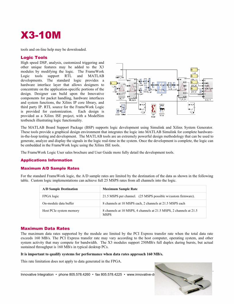
Logic ToolsHigh speed DSP, analysis, customized triggering andother unique features may be added to the X3modules by modifying the logic. The FrameWorkLogic tools support RTL and MATLABdevelopments. The standard logic provides ahardware interface layer that allows designers toconcentrate on the application-specific portions of thedesign. Designer can build upon the Innovativecomponents for packet handling, hardware interfacesand system functions, the Xilinx IP core library, andthird party IP. RTL source for the FrameWork Logicis provided for customization. Each design isprovided as a Xilinx ISE project, with a ModelSimtestbench illustrating logic functionality.
The MATLAB Board Support Package (BSP) supports logic development using Simulink and Xilinx System Generator.These tools provide a graphical design environment that integrates the logic into MATLAB Simulink for complete hardware-in-the-loop testing and development. The MATLAB tools are an extremely powerful design methodology that can be used togenerate, analyze and display the signals in the logic real-time in the system. Once the development is complete, the logic canbe embedded in the FrameWork logic using the Xilinx ISE tools.
The FrameWork Logic User sales brochure and User Guide more fully detail the development tools.
Applications Information
Maximum A/D Sample Rates
For the standard FrameWork logic, the A/D sample rates are limited by the destination of the data as shown in the followingtable. Custom logic implementations can achieve full 25 MSPS rates from all channels into the logic.
A/D Sample Destination Maximum Sample Rate
FPGA logic 21.5 MSPS per channel. (25 MSPS possible w/custom firmware).
On-module data buffer 8 channels at 10 MSPS each, 2 channels at 21.5 MSPS each
Host PCIe system memory 8 channels at 10 MSPS, 4 channels at 21.5 MSPS, 2 channels at 21.5 MSPS
Maximum Data RatesThe maximum data rates supported by the module are limited by the PCI Express transfer rate when the total data rateexceeds 160 MB/s. The PCI Express transfer rate may vary according to the host computer, operating system, and othersystem activity that may compete for bandwidth. The X3 modules support 250MB/s full duplex during bursts, but actualsustained throughput is 160 MB/s in typical desktop PCs.
It is important to qualify systems for performance when data rates approach 160 MB/s.
This rate limitation does not apply to data generated in the FPGA.
Innovative Integration • phone 805.578.4260 • fax 805.578.4225 • www.innovative-dsp.com 12 of 15
X3-10MCablesX3 modules uses a shielded, jacketed 68-wire cable assembly for the front panel IO. The pleated copper foil shield cable is“near coax” in its performance. This cable, plus the use of differential signals and use of ground signals as shields, producethe best results. A screw terminal assembly is available. See available cable options online here.
XMC Adapter CardsXMC modules can be used in standard desktop system, compact PCI/PXI using an adapter card. Adapters for cabled PCIExpress (CPEX) and VPX are also available. All adapter cards are software transparent.
The X3 modules use the auxiliary P16 connector for digital IO and additional clock inputs. A total of 44 bits of digital IO,directly connected to the application FPGA, are routed to the rear edge MDR connector as 22 balanced differential pairssupporting LVDS or lower speed single-ended LVCMOS signals. The X3 modules also have a sample clock input and PLLreference input to J16. The cPCI/PXI adapter uses these to connect to system clocks, while the PCIe desktop adapterprovides SMB input connectors for system clock inputs. See available carrier options online here.
PCIe-XMC Adapter (80172)
x1 PCIe to XMC
SMB Clock and trigger inputs
PCI-XMC Adapter (80167)
64-bit, 133 MHz PCI-X host
x4 PCIe to XMC
Compact PCI-XMC Adapter (80207)
64-bit, 133 MHz PCI-X host
x4 PCIe to XMC
PXI triggers and clock support
Innovative Integration • phone 805.578.4260 • fax 805.578.4225 • www.innovative-dsp.com 13 of 15

X3-10MApplications that need remote or portable IO can use either the eInstrument PC or eInstrument Node with X3 modules. See available intelligent carrier options online here.
eInstrument PC with Dual PCI Express XMC Modules (90201)Windows/Linux embedded PC
8x USB, GbE, cable PCIe, VGA
High speed x8 interconnect between modules
GPS disciplined, programmable sample clocks and triggers to XMCs
Up to 400MB/s data logging using SSD
12V operation
eInstrument DAQ Node – Remote IO using cabled PCI Express
(90181)
PCI Express system expansion
Up to 7 meter cable
electrically isolated from host computer
software transparent
eInstrument PC with Dual PCI Express XMC Modules (90271)Windows/Linux embedded PC
6x USB, GbE, 8x cable PCIe, DisplayPort
High speed x4 PCIe + Aurora interconnect between modules
GPS disciplined, programmable sample clocks and triggers to XMCs
Up to 500MB/s data logging using SSD
Innovative Integration • phone 805.578.4260 • fax 805.578.4225 • www.innovative-dsp.com 14 of 15
X3-10MIMPORTANT NOTICESInnovative Integration Incorporated reserves the right to make corrections, modifications, enhancements, improvements, andother changes to its products and services at any time and to discontinue any product or service without notice. Customersshould obtain the latest relevant information before placing orders and should verify that such information is current andcomplete. All products are sold subject to Innovative Integration’s terms and conditions of sale supplied at the time of orderacknowledgment.
Innovative Integration warrants performance of its hardware products to the specifications applicable at the time of sale inaccordance with Innovative Integration’s standard warranty. Testing and other quality control techniques are used to theextent Innovative Integration deems necessary to support this warranty. Except where mandated by governmentrequirements, testing of all parameters of each product is not necessarily performed.
Innovative Integration assumes no liability for applications assistance or customer product design. Customers are responsiblefor their products and applications using Innovative Integration products. To minimize the risks associated with customerproducts and applications, customers should provide adequate design and operating safeguards.
Innovative Integration does not warrant or represent that any license, either express or implied, is granted under anyInnovative Integration patent right, copyright, mask work right, or other Innovative Integration intellectual property rightrelating to any combination, machine, or process in which Innovative Integration products or services are used. Informationpublished by Innovative Integration regarding third-party products or services does not constitute a license from InnovativeIntegration to use such products or services or a warranty or endorsement thereof. Use of such information may require alicense from a third party under the patents or other intellectual property of the third party, or a license from InnovativeIntegration under the patents or other intellectual property of Innovative Integration.
Reproduction of information in Innovative Integration data sheets is permissible only if reproduction is without alteration andis accompanied by all associated warranties, conditions, limitations, and notices. Reproduction of this information withalteration is an unfair and deceptive business practice.
Innovative Integration is not responsible or liable for such altered documentation. Resale of Innovative Integration productsor services with statements different from or beyond the parameters stated by Innovative Integration for that product orservice voids all express and any implied warranties for the associated Innovative Integration product or service and is anunfair and deceptive business practice. Innovative Integration is not responsible or liable for any such statements.
For further information on Innovative Integration products and support see our web site:
www.innovative-dsp.com
Mailing Address: Innovative Integration, Inc.
2390A Ward Avenue, Simi Valley, California 93065
Copyright ©2007, Innovative Integration, Incorporated
Innovative Integration • phone 805.578.4260 • fax 805.578.4225 • www.innovative-dsp.com 15 of 15