wolfspeed cghv40100; 100 w, dc - 3.0 ghz, 50 v, gan hemt
TRANSCRIPT

Rev 3.6 - April 2020 4600 Silicon Drive | Durham, NC 27703 | wolfspeed.com
Large Signal Models Available for ADS and MWO
CGHV40100100 W, DC - 3.0 GHz, 50 V, GaN HEMT
Description
Cree’s CGHV40100 is an unmatched, gallium nitride (GaN) high electron mobility transistor (HEMT). The CGHV40100, operating from a 50 volt rail, offers a general purpose, broadband solution to a variety of RF and microwave applications. GaN HEMTs offer high efficiency, high gain and wide bandwidth capabilities making the CGHV40100 ideal for linear and compressed amplifier circuits. The transistor is available in a 2-lead flange and pill package.
Package Types: 440193 & 440206PN: CGHV40100F & CGHV40100P
Typical Performance Over 500 MHz - 2.5 GHz (TC = 25˚C), 50 V
Notes: Measured CW in the CGHV40100F-AMP application circuit.
Features
• Up to 3 GHz Operation• 100 W Typical Output Power• 17.5 dB Small Signal Gain at 2.0 GHz• Application Circuit for 0.5 - 2.5 GHz• 55% Efficiency at PSAT• 50 V Operation
Parameter 500 MHz 1.0 GHz 1.5 GHz 2.0 GHz 2.5 GHz UnitsSmall Signal Gain 17.6 16.9 17.7 17.5 14.8 dB
Saturated Output Power 147 100 141 116 112 W
Drain Efficiency @ PSAT 68 56 58 54 54 %
Input Return Loss 6 5.1 10.5 5.5 8.8 dB

CGHV40100 2
Rev 3.6 - April 2020 4600 Silicon Drive | Durham, NC 27703 | wolfspeed.com
Absolute Maximum Ratings (not simultaneous) at 25˚C Case Temperature
Notes:1 Current limit for long term, reliable operation2 Refer to the Application Note on soldering at wolfspeed.com/rf/document-library3 Measured for the CGHV40100P at PDISS = 83 W4 Measured for the CGHV40100F at PDISS = 83 W5 See also, Power Derating Curve on Page 5
Electrical Characteristics (TC = 25˚C)
Notes:1 Measured on wafer prior to packaging2 Scaled from PCM data3 Measured in CGHV40100-AMP4 PSAT is defined as IG = 0.208 mA5 Includes package
Parameter Symbol Rating Units ConditionsDrain-Source Voltage VDSS 150 Volts 25˚C
Gate-to-Source Voltage VGS -10, +2 Volts 25˚C
Storage Temperature TSTG -65, +150 ˚C
Operating Junction Temperature TJ 225 ˚C
Maximum Forward Gate Current IGMAX 20.8 mA 25˚C
Maximum Drain Current1 IDMAX 8.7 A 25˚C
Soldering Temperature2 TS 245 ˚C
Screw Torque τ 40 in-oz
Thermal Resistance, Junction to Case3 RθJC 1.62 ˚C/W 85˚C
Thermal Resistance, Junction to Case4 RθJC 1.72 ˚C/W 85˚C
Case Operating Temperature5 TC -40, +150 ˚C
Characteristics Symbol Min. Typ. Max. Units ConditionsDC Characteristics1
Gate Threshold Voltage VGS(th) -3.8 -3.0 -2.3 VDC VDS = 10 V, ID = 20.8 mA
Gate Quiescent Voltage VGS(Q) – -2.7 – VDC VDS = 50 V, ID = 0.6 A
Saturated Drain Current2 IDS 13.5 19.3 – A VDS = 6.0 V, VGS = 2.0 V
Drain-Source Breakdown Voltage VBR 100 – – VDC VGS = -8 V, ID = 20.8 mA
RF Characteristics3 (TC = 25˚C, F0 = 2.0 GHz unless otherwise noted)
Small Signal Gain GSS 16 17.5 – dB VDD = 50 V, IDQ = 0.6 A
Power Gain GP – 11.0 – dB VDD = 50 V, IDQ = 0.6 A, POUT = PSAT
Output Power at Saturation4 PSAT 100 116 – W VDD = 50 V, IDQ = 0.6 A
Drain Efficiency η 47 54 – % VDD = 50 V, IDQ = 0.6 A, POUT = PSAT
Output Mismatch Stress VSWR – – 10 : 1 Y No damage at all phase angles, VDD = 50 V, IDQ = 0.6 A, POUT = 100 W CW
Dynamic Characteristics5
Input Capacitance CGS – 29.3 – pF VDS = 50 V, Vgs = -8 V, f = 1 MHz
Output Capacitance CDS – 7.3 – pF VDS = 50 V, Vgs = -8 V, f = 1 MHz
Feedback Capacitance CGD – 0.61 – pF VDS = 50 V, Vgs = -8 V, f = 1 MHz

CGHV40100 3
Rev 3.6 - April 2020 4600 Silicon Drive | Durham, NC 27703 | wolfspeed.com
4
8
12
16
20
24
Gai
n,R
etur
nLo
ss(d
B)
Small Signal S-parametersCGHV40100F in Applications Circuit
Vdd = 50 V, Idq = 600 mA, Tcase = 25°C
S11S21S22
-16
-12
-8
-4
0
0.0 0.5 1.0 1.5 2.0 2.5 3.0
Gai
n,R
etur
nLo
ss(d
B)
Frequency (GHz)
Figure 1. Small Signal Gain and Return Losses versus Frequency measured in application circuit CGHV40100-AMP VDD = 50 V, IDQ = 600 mA, Tcase = 25°C
Gain
, Ret
urn
Loss
(dB)
Frequency (GHz)
Figure 2.Output Power and Drain Efficiency vs Frequency
VDD = 50 V, IDQ = 600 mA
Pout
(dBm
), Dr
ain
Effic
ienc
y (%
)
Gain
(dB)
Frequency (GHz)
CGHV40100 Typical Performance
22
24
26
28
30
32
34
36
38
54
56
58
60
62
64
66
68
70G
ain
(dB
)
Pout
(dB
m),
Dra
inEf
ficie
ncy
(%)
CGHV40100F in Applications CircuitVdd = 50 V, Idq = 600 mA, Tcase = 25°C
CW @ Psat
Output Power
Drain Efficiency
Gain
8
10
12
14
16
18
20
22
40
42
44
46
48
50
52
54
0.25 0.50 0.75 1.00 1.25 1.50 1.75 2.00 2.25 2.50 2.75
Pout
(dB
m),
Dra
inEf
ficie
ncy
(%)
Frequency (GHz)
Drain Efficiency
Output Power
Gain

CGHV40100 4
Rev 3.6 - April 2020 4600 Silicon Drive | Durham, NC 27703 | wolfspeed.com
-30
-25
-20
-15
-10
-5
0
IMD
3(d
Bc)
CGHV40100F in Applications CircuitVdd = 50 V, Idq = 600 mA, Tcase = 25°C
1 MHz Two Tone Spacing
0.5 GHz
1.5 GHz
2.5 GHz
-60
-55
-50
-45
-40
-35
-30
27 29 31 33 35 37 39 41 43 45 47Average Output Power (dBm)
Figure 3. Third Order Intermodulation Distortion vs Average Output Power measured in Broadband Amplifier Circuit CGHV40100-AMP
Spacing = 1 MHz, VDD = 50 V, IDQ = 600 mA, Tcase = 25°CIM
D3 (d
Bc)
Average Output Power (dBm)
Figure 4. Third Order Intermodulation Distortion vs Frequency measured in Broadband Amplifier Circuit CGHV40100-AMP
Spacing = 1 MHz, VDD = 50 V, IDQ = 600 mA, Tcase = 25°C
IMD3
(dBc
)
Frequency (GHz)
CGHV40100 Typical Performance
-30
-25
-20
-15
-10
-5
0
IMD
3(d
Bc)
CGHV40100F in Applications CircuitVdd = 50 V, Idq = 600 mA, Tcase = 25°C
1 MHz Two Tone Spacing @ 10W Average Pout
-60
-55
-50
-45
-40
-35
-30
0.25 0.50 0.75 1.00 1.25 1.50 1.75 2.00 2.25 2.50 2.75Frequency (GHz)

CGHV40100 5
Rev 3.6 - April 2020 4600 Silicon Drive | Durham, NC 27703 | wolfspeed.com
CGHV40100 Typical Performance
G MAX
(dB)
K-Fa
ctor
Frequency (GHz)
0.5
0.75
1
1.25
30
35
40
45
K-F
acto
r
GM
AX(d
B)
Maximum Avaliable Gain & K-FactorCGHV40100
Vdd = 50 V, Idq = 600 mA, Tcase = 25°C
Gmax
K-Factor
0
0.25
0.5
20
25
30
0.0 0.5 1.0 1.5 2.0 2.5 3.0 3.5 4.0Frequency (GHz)
Figure 5. GMAX and K-Factor vs Frequency VDD = 50 V, IDQ = 600 mA, Tcase = 25°C

CGHV40100 6
Rev 3.6 - April 2020 4600 Silicon Drive | Durham, NC 27703 | wolfspeed.com
CGHV40100-AMP Application Circuit Schematic
CGHV40100-AMP Application Circuit
CGHV40100 7
Rev 3.6 - April 2020 4600 Silicon Drive | Durham, NC 27703 | wolfspeed.com
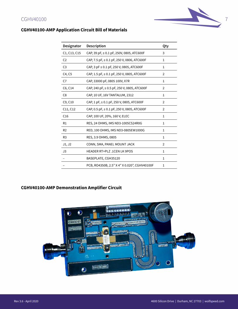
CGHV40100-AMP Application Circuit Bill of Materials
CGHV40100-AMP Demonstration Amplifier Circuit
Designator Description Qty
C1, C13, C15 CAP, 39 pF, ± 0.1 pF, 250V, 0805, ATC600F 3
C2 CAP, 7.5 pF, ± 0.1 pF, 250 V, 0806, ATC600F 1
C3 CAP, 3 pF ± 0.1 pF, 250 V, 0805, ATC600F 1
C4, C5 CAP, 1.5 pF, ± 0.1 pF, 250 V, 0805, ATC600F 2
C7 CAP, 33000 pF, 0805 100V, X7R 1
C6, C14 CAP, 240 pF, ± 0.5 pF, 250 V, 0805, ATC600F 2
C8 CAP, 10 UF, 16V TANTALUM, 2312 1
C9, C10 CAP, 1 pF, ± 0.1 pF, 250 V, 0805, ATC600F 2
C11, C12 CAP, 0.5 pF, ± 0.1 pF, 250 V, 0805, ATC600F 2
C16 CAP, 100 UF, 20%, 160 V, ELEC 1
R1 RES, 24 OHMS, IMS ND3-1005CS24R0G 1
R2 RED, 100 OHMS, IMS ND3-0805EW1000G 1
R3 RES, 3.9 OHMS, 0805 1
J1, J2 CONN, SMA, PANEL MOUNT JACK 2
J3 HEADER RT>PLZ .1CEN LK 9POS 1
– BASEPLATE, CGH35120 1
– PCB, RO4350B, 2.5” X 4” X 0.020”, CGHV40100F 1
CGHV40100 8
Rev 3.6 - April 2020 4600 Silicon Drive | Durham, NC 27703 | wolfspeed.com
0
10
20
30
40
50
60
70
80
90
1.10 1.15 1.20 1.25 1.30 1.35 1.40 1.45 1.50
Out
put P
ower
(dB
m),
Effic
ienc
y (%
), G
ain
(dB
)
Frequency (GHz)
Pout (dBm)Gain (dB)Efficiency (%)
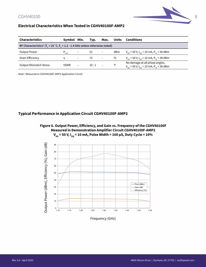
Electrical Characteristics When Tested in CGHV40100F-AMP2
Typical Performance in Application Circuit CGHV40100F-AMP2
Figure 6. Output Power, Efficiency, and Gain vs. Frequency of the CGHV40100FMeasured in Demonstration Amplifier Circuit CGHV40100F-AMP2
VDD = 50 V, IDQ = 10 mA, Pulse Width = 100 μS, Duty Cycle = 10%
Out
put P
ower
(dBm
), Eff
icie
ncy
(%),
Gain
(dB)
Frequency (GHz)
Note1: Measured in CGHV40100F-AMP2 Application Circuit
Characteristics Symbol Min. Typ. Max. Units Conditions
RF Characteristics1 (TC = 25˚C, F0 = 1.2 - 1.4 GHz unless otherwise noted)
Output Power POUT – 51 – dBm VDD = 50 V, IDQ = 10 mA, PIN = 38 dBm
Drain Efficiency η – 72 – % VDD = 50 V, IDQ = 10 mA, PIN = 38 dBm
Output Mismatch Stress VSWR – 10 : 1 – YNo damage at all phase angles, VDD = 50 V, IDQ = 10 mA, PIN = 38 dBm

CGHV40100 9
Rev 3.6 - April 2020 4600 Silicon Drive | Durham, NC 27703 | wolfspeed.com
6 59 8 7 34 2 1
CGHV40100F-AMP2 Demonstration Amplifier Circuit Schematic
CGHV40100F-AMP2 Demonstration Amplifier Circuit Outline

CGHV40100 10
Rev 3.6 - April 2020 4600 Silicon Drive | Durham, NC 27703 | wolfspeed.com
CGHV40100F-AMP2 Bill of Materials
Designator Description Qty
C1 CAP, 2.0pF, +/-0.1pF, 0603, ATC 1
R2 RES, 1/16W, 0603, 1%, 20 Ohms 1
R4 RES,1/16W,0603,1%,4.99K OHMS 1
R1, R3 RES, AlN, 50.0 OHM, +/- 5%, 0505, PtAg TERMINATION 1
C8 CAP, 10UF, 10%, 1206, 16V 1
C1, C5, C17 CAP, 100.0pF, +/-5%, 0603, ATC 3
C16 CAP, 12.0pF, +/-5%, 0603, ATC600 1
C14 CAP, 20.0pF, +/-5%, 0603, ATC600S 1
C4 CAP, 43pF,+/-5%pF, 0603, ATC 1
C10, C11 CAP, 47pF,+/-5%pF, 0603, ATC 2
C3 CAP, 56PF +/- 5%, 0603 , ATC600S 1
C2, C9 CAP, 5.1PF, +/-0.05 PF, 0603, 600S 2
C6, C12 CAP,0805,100V,TEMP STBL,1000PF 2
C7, C13 CAP, 10000PF, +/-10%, 0805, X7R, 100V, TEMP STBL 2
– PCB, RO4350, 0.020 THK, CGHV40100F-TB2 1.2-1.4GHz RADAR 1
– BASEPLATE, AL, 4.00 X 2.50 X 0.49 FOR THRU HOLE CAPACITORS 1
– 2-56 SOC HD SCREW 1/4 SS 4
– #2 SPLIT LOCKWASHER SS 4
J2, J3 CONN, SMA, PANEL MOUNT JACK, FLANGE, 4-HOLE, BLUNT POST 2
J4 CONN, SMB, STRAIGHT JACK RECEPTACLE, SMT, 50 OHM, Au PLATED 1
J1 HEADER RT>PLZ .1CEN LK 9POS 1
W1 WIRE, BLACK, 18 AWG, EXTRUDED TFE TEFLON 1
L1 INDUCTOR,CHIP,2.2nH,0603 SMT 1
C2 CAP, 6.8pF, +/- 0.25 pF, 0603, ATC 1
C15 CAP, 100uF, +/-20%, 100V, ALUM ELEC 1
Q1 Transistor CGHV40100F 1
–

CGHV40100 11
Rev 3.6 - April 2020 4600 Silicon Drive | Durham, NC 27703 | wolfspeed.com
D
Z Source Z Load
G
S
Note 1. VDD = 50 V, IDQ = 600 mA in the 440193 package Note 2. Optimized for power gain, PSAT and PAE
Source and Load Impedances
Electrostatic Discharge (ESD) Classifications
Parameter Symbol Class Test Methodology
Human Body Model HBM 1A (> 250 V) JEDEC JESD22 A114-D
Charge Device Model CDM 2 (125 V to 250 V) JEDEC JESD22 C101-C
Frequency (MHz) Z Source Z Load
500 0.43 + j5.25 8.83 + j0.85
750 0.40 + j2.62 10.78 + j2.50
1000 0.30 + j1.31 9.06 + 4.23
1250 0.30 + j0.44 7.40 + j3.85
1500 0.30 - j0.44 6.39 + j3.44
1750 0.25 - j0.87 4.41 + j3.03
2000 0.25 - j1.31 3.68 + j2.17
2250 0.25 - j2.18 3.42 + j2.17
2500 0.26 - j2.62 2.65 + j1.74

CGHV40100 12
Rev 3.6 - April 2020 4600 Silicon Drive | Durham, NC 27703 | wolfspeed.com
Product Dimensions CGHV40100F (Package Type — 440193)
Product Dimensions CGHV40100P (Package Type — 440206)
CGHV40100 13
Rev 3.6 - April 2020 4600 Silicon Drive | Durham, NC 27703 | wolfspeed.com
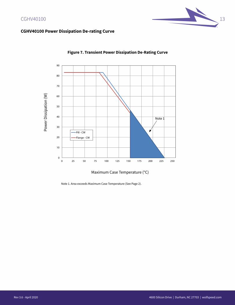
CGHV40100 Power Dissipation De-rating Curve
Pow
er D
issi
patio
n (W
)
Maximum Case Temperature (°C)
0
10
20
30
40
50
60
70
80
90
0 25 50 75 100 125 150 175 200 225 250
Pow
er D
issi
patio
n (W
)
Maximum Case Temperature (°C)
Pill - CW
Flange - CW
Figure 7. Transient Power Dissipation De-Rating Curve
Note 1. Area exceeds Maximum Case Temperature (See Page 2).
Note 1

CGHV40100 14
Rev 3.6 - April 2020 4600 Silicon Drive | Durham, NC 27703 | wolfspeed.com
Part Number System
Table 1.
Table 2.
Parameter Value Units
Upper Frequency1 4.0 GHz
Power Output 100 W
Package Flange -
Character Code Code Value
A 0
B 1
C 2
D 3
E 4
F 5
G 6
H 7
J 8
K 9
Examples: 1A = 10.0 GHz2H = 27.0 GHz
Note1: Alpha characters used in frequency code indicate a value greater than 9.9 GHz. See Table 2 for value.
Package
Power Output (W)
Upper Frequency (GHz)
Cree GaN High Voltage
CGHV40100F

CGHV40100 15
Rev 3.6 - April 2020 4600 Silicon Drive | Durham, NC 27703 | wolfspeed.com
Product Ordering Information
Order Number Description Unit of Measure Image
CGHV40100F GaN HEMT Each
CGHV40100P GaN HEMT Each
CGHV40100F-AMP
Test board with GaN HEMT (CGHV40100F) installed, operating from 0.5 - 2.5 GHz for communications or ISM applications.
Each
CGHV40100F-AMP2Test board with GaN HEMT (CGHV40100F) installed, operating from 1.2 - 1.4 GHz for L-Band Radar.

CGHV40100 16
Rev 3.6 - April 2020 4600 Silicon Drive | Durham, NC 27703 | wolfspeed.com
NotesDisclaimer
Specifications are subject to change without notice. Cree, Inc. believes the information contained within this data sheet to be accurate and reliable. However, no responsibility is assumed by Cree for any infringement of patents or other rights of third parties which may result from its use. No license is granted by implication or otherwise under any patent or pat-ent rights of Cree. Cree makes no warranty, representation or guarantee regarding the suitability of its products for any particular purpose. “Typical” parameters are the average values expected by Cree in large quantities and are provided for information purposes only. These values can and do vary in different applications and actual performance can vary over time. All operating parameters should be validated by customer’s technical experts for each application. Cree products are not designed, intended or authorized for use as components in applications intended for surgical implant into the body or to support or sustain life, in applications in which the failure of the Cree product could result in personal injury or death or in applications for planning, construction, maintenance or direct operation of a nuclear facility.
© 2014-2020 Cree, Inc. All rights reserved. Wolfspeed® and the Wolfspeed logo are registered trademarks of Cree, Inc.
For more information, please contact:
4600 Silicon DriveDurham, North Carolina, USA 27703www.wolfspeed.com/RF
Sales Contact [email protected]