wireless power transmitter for smartphones with fast
TRANSCRIPT

Wireless Power Transmitter for Smartphones with Fast Charging Modes for 5W, 7.5W, and 10W Applications
P9241-G Datasheet
© 2019 Integrated Device Technology, Inc. 1 March 8, 2019
CS
P
CS
N
VIN
Peak
Detector
VD
EM
1
Coi
l Ass
embl
y
P9241-G
SW_S
LDO33
LDO18
PREG
GP
IO_B
8
LED
1
LED
2
VIN_LDO
RSNS
GH_BRG1
SW_BRG1
GL_BRG1
GH_BRG2
SW_BRG2
GL_BRG2
LP
CP
Clock IC GPIO_B6GNDG
PIO
_A2
Step-Down
Regulator
Description
The P9241-G is a highly integrated, magnetic induction, wireless power transmitter that supports Baseline Power Profile (BPP), 7.5W wireless charging for iPhone mode, and 10W wireless charging for Android proprietary modes. The external step down regulator in the front end of P9241-G design enables wide input voltage range of 5V to 19V.
The P9241-G transmitter IC integrates an industry-leading 32-bit ARM® Cortex®-M0 processor, offering a high level of program-mability and extremely low standby power consumption. Integrated current sense amplifier, full bridge MOSFET drivers, and bias regulators reduces the component count of the solution and differentiates the P9241-G from the competition.
The P9241-G transmitter generates power through the power coil, detects the presence of a wireless power receiver, decodes the communication packets from the receiver, and adjusts the transmitted power by controlling the voltage based on feedback from the receiver. The device is specially designed to support A11a coil configuration and goes into fixed-frequency operation mode to support 7.5W charging for Apple iPhones. It uses an external oscillator for very accurate 127.7kHz fixed frequency operation.
The P9241-G features two LED outputs with pre-defined user-programmable blinking patterns for end-user indication, which supports a wide range of applications. The transmitter detects if a foreign metal object is placed on the transmitter pad by measuring the power loss between the received power and the transmitted power during the Power Transfer Phase. The I2C serial communication allows the user to read the transmitter’s basic infor-mation, such as voltage, current, frequency, and fault conditions.
The P9241-G also features a wide range of system protections, such as over-current, over-voltage, under-voltage lockout, and thermal management circuits to safe guard wireless power systems under fault conditions.
The device is available in a lead-free, space-saving 48-VFQFPN package. The product is rated for a -40ºC to +85ºC operating temperature range.
Typical Applications
BPP Wireless Charging Pads
Up to 7.5W charging for iPhones
Up to 10W Android Fast Charging Pads
Cradles
Tablets
After-Market Automotive WirelessCharging Pads
Features
Supports 7.5W wireless charging for iOS iPhones
Supports 10W wireless charging for Android phones
Fixed frequency operation for iPhones
Wide input voltage range: 5V to 19V
WPC-1.2.4 compatible, A11a coil configuration
EN303417 CE certification compatible
Feedback control for external input step-down regulator
Integrated drivers for external power MOSFETs
Embedded 32-bit ARM® Cortex®-M0 processor (trademark ofARM, Ltd.)
Voltage and current demodulation scheme for WPCcommunication
Integrated current sense amplifier
Low standby power
Dedicated remote temperature sensing
User-programmable power transfer LED indicators
User-programmable foreign objects detection (FOD)
Active-LOW enable pin for electrical on/off
Over-current and over-temperature protection
Supports I2C interface
-40 to +85°C ambient operating temperature range
48-VFQFPN (6 6 mm) RoHS-compliant package
Typical Application Circuit

P9241-G Datasheet
© 2019 Integrated Device Technology, Inc. 2 March 8, 2019
Contents
1. Pin Assignments ...........................................................................................................................................................................................5
2. Pin Descriptions ............................................................................................................................................................................................6
3. Absolute Maximum Ratings ..........................................................................................................................................................................8
4. Electrical Characteristics ..............................................................................................................................................................................9
5. Typical Performance Characteristics ..........................................................................................................................................................11
6. Block Diagram ............................................................................................................................................................................................16
7. General Description ....................................................................................................................................................................................17
8. WPC Mode Characteristics ........................................................................................................................................................................18
8.1 Selection Phase .................................................................................................................................................................................18
8.2 Ping Phase (Digital Ping) ...................................................................................................................................................................18
8.3 Identification and Configuration Phase ..............................................................................................................................................19
8.4 Power Transfer Phase .......................................................................................................................................................................19
9. Application Information ...............................................................................................................................................................................20
9.1 Internal Power Supply and Internal Bias............................................................................................................................................20
9.1.1 Integrated Step-Down Regulator ........................................................................................................................................20
9.1.2 Linear Regulators – PREG, LDO33, and LDO18 ...............................................................................................................20
9.2 Enable Pin .........................................................................................................................................................................................20
9.3 Software Under-Voltage Lock-Out (UVLO) Protection ......................................................................................................................20
9.4 Die Temperature Protection ..............................................................................................................................................................21
9.5 External Temperature Sensing – TS .................................................................................................................................................21
9.6 Full-Bridge Driver ...............................................................................................................................................................................21
9.7 LC Resonant Circuits .........................................................................................................................................................................21
9.8 WPC Communication Interface .........................................................................................................................................................22
9.8.1 Modulation/Communication ................................................................................................................................................22
9.8.2 Bit Decoding Scheme for ASK ............................................................................................................................................23
9.8.3 ASK Voltage Demodulation – VDEM1 Pin..........................................................................................................................23
9.8.4 ASK Current Demodulation – IDEMI Pin ............................................................................................................................24
9.9 General Purpose Input/output – GPIO Pins ......................................................................................................................................24
9.9.1 Input Port Detection and Receiver Support – GPIO_A5, GPIO_A7, and GPIO_B8 ...........................................................24
9.9.2 Foreign Object Detection – GPIO_A3 ................................................................................................................................25
9.9.3 Control of External Power Stage DC/DC Buck Regulator – GPIO_B4 and GPIO_B7 ........................................................26
9.9.4 Bypass External DC/DC Buck Regulator– GPIO_A4 .........................................................................................................26
9.9.5 Coil Over-Voltage Control – GPIO_A6 ...............................................................................................................................26
9.9.6 External Oscillator– GPIO_B5 and GPIO_B6 .....................................................................................................................26
9.9.7 LED Pattern Selection – GPIO_A3 .....................................................................................................................................27
9.9.8 I2C Communication Interface – GPIO_A0 and GPIO_A1 ...................................................................................................28
9.9.9 External Memory – GPIO_B0, GPIO_B1, GPIO_B2, and GPIO_B3 ..................................................................................29
10. Register Addresses and Definitions ...........................................................................................................................................................29

P9241-G Datasheet
© 2019 Integrated Device Technology, Inc. 3 March 8, 2019
11. Power Dissipation and Thermal Requirements ..........................................................................................................................................33
11.1 Typical Application Schematic ...........................................................................................................................................................33
11.2 Bill of Materials (BOM) .......................................................................................................................................................................35
12. Package Outline Drawings .........................................................................................................................................................................38
13. Special Notes: P9241-G 48-VFQFPN Package Assembly .........................................................................................................................38
14. Marking Diagram ........................................................................................................................................................................................38
15. Ordering Information ...................................................................................................................................................................................38
16. Revision History ..........................................................................................................................................................................................39
List of Figures
Figure 1. Pin Assignments ..................................................................................................................................................................................5
Figure 2. Efficiency vs. Output Load: VOUT_RX = 5V ...........................................................................................................................................11
Figure 3. Full Load Efficiency and Charging Map vs. XY Positions (in mm scale): Vin = 12V, Vout = 5V, Spacer = 2.5mm ..........................11
Figure 4. Internal Buck Load Regulation ..........................................................................................................................................................12
Figure 5. Load Regulation vs. Output Load: LDO33 .........................................................................................................................................12
Figure 6. Load Regulation vs. Output Load: LDO18 .........................................................................................................................................13
Figure 7. Voltage and Current Signal for Demodulation: Ch2 = VSNS, Ch3 = ISNS_IN ..................................................................................13
Figure 8. USB Adaptor Start-up: Ch1 = VBRIDGE, Ch2 = Vin, Ch3 = D-, Ch4 = D+ .......................................................................................14
Figure 9. 19V Fixed Voltage Adaptor Start-up: Ch1 = VBRIDGE, Ch2 = Vin, Ch3 = GPIO_B4, Ch4 = iIn .......................................................14
Figure 10. Enable and Disable of External Buck Regulator: Ch1 = VBRIDGE, Ch2 = Tx_SW, Ch3 = GPIO_B4 ...............................................15
Figure 11. Block Diagram ...................................................................................................................................................................................16
Figure 12. WPC Power Transfer Phases Flowchart ...........................................................................................................................................18
Figure 13. UVLO Threshold Definition ................................................................................................................................................................20
Figure 14. NTC Thermistor Connection to the TS Pin ........................................................................................................................................21
Figure 15. Example of Differential Bi-phase Encoding for FSK ..........................................................................................................................22
Figure 16. Example of Asynchronous Serial Byte Format for FSK .....................................................................................................................22
Figure 17. Bit Decoding Scheme ........................................................................................................................................................................23
Figure 18. Byte Decoding Scheme .....................................................................................................................................................................23
Figure 19. Communication Packet Structure ......................................................................................................................................................23
Figure 20. Voltage Mode Envelope Detector ......................................................................................................................................................23
Figure 21. Current Mode Envelope Detector ......................................................................................................................................................24
Figure 22. I2C Access Read Protocol and Write Protocol ...................................................................................................................................28
Figure 23. P9241-G Typical Application Schematic V3.8 ...................................................................................................................................34

P9241-G Datasheet
© 2019 Integrated Device Technology, Inc. 4 March 8, 2019
List of Tables
Table 1. Pin Descriptions ...................................................................................................................................................................................6
Table 2. Absolute Maximum Ratings .................................................................................................................................................................8
Table 3. Package Thermal Information .............................................................................................................................................................8
Table 4. ESD Information ..................................................................................................................................................................................8
Table 5. Electrical Characteristics .....................................................................................................................................................................9
Table 6. Input Voltage vs. Receiver Supported ...............................................................................................................................................25
Table 7. Voltage on GPIO_A3 vs. FOD Threshold ..........................................................................................................................................26
Table 8. Resistors for Setting the LED Pattern ................................................................................................................................................27
Table 9. Read Register – Device ID Register ..................................................................................................................................................29
Table 10. Read Register – Firmware Revision ..................................................................................................................................................29
Table 11. Read Register – State Register .........................................................................................................................................................29
Table 12. Read Register – Error Code Register ................................................................................................................................................30
Table 13. Read Register – Adaptor Type Register ............................................................................................................................................30
Table 14. Read Register – Potential Power Register ........................................................................................................................................30
Table 15. Read Register – Input Current ...........................................................................................................................................................30
Table 16. Read Register – Input Voltage ..........................................................................................................................................................31
Table 17. Read Register – Remote Temperature Sensing Voltage ..................................................................................................................31
Table 18. Read Register – Operating Frequency ..............................................................................................................................................31
Table 19. Read Register – Transmitter Duty Cycle ...........................................................................................................................................31
Table 20. Read Register – Transmitter Power 32 Bit ........................................................................................................................................31
Table 21. Read Register – Received Power Packet Value 32 Bit .....................................................................................................................32
Table 22. Read Register – FOD Threshold 16 Bit .............................................................................................................................................32
Table 23. P9241-G Evaluation Kit V3.8 Bill of Materials ....................................................................................................................................35

P9241-G Datasheet
© 2019 Integrated Device Technology, Inc. 5 March 8, 2019
1. Pin Assignments
Figure 1. Pin Assignments
1
2
3
4
5
6
7
8
9
10
13 14 15 16 17 18 19 20 21 22
48 47 46 45 44 43 42 41 40 39
36
35
34
33
32
31
30
29
28
27
EP (Center Exposed Pad)
GND
PREG
VIN
SW_S
GND1
VIN_LDO
LED1
GP
IO_B
5
GP
IO_B
6
GP
IO_A
0
GP
IO_A
1
GP
IO_A
2
GP
IO_A
3
AG
IO_A
4
GP
IO_A
5
GP
IO_A
6
GP
IO_A
7
SW_BRG1
GL_BRG1
GND2
GL_BRG2
SW_BRG2
BST_BRG2
GH_BRG2
GPIO_B4
GPIO_B3
GPIO_B2
CS
P
CS
N
ISN
S_O
UT
IDE
MI
VD
EM
1
VB
RG
_IN
DR
V_V
IN
11
12
LED2
VDDIO
26
25
BPIO_B1
GPIO_B0
23 24
38 37
GP
IO_B
7
GP
IO_B
8
GH
_BR
G1
BS
T_B
RG
1
VD
EM
2
TS
EN
GN
D3
LDO33
LDO18

P9241-G Datasheet
© 2019 Integrated Device Technology, Inc. 6 March 8, 2019
2. Pin Descriptions
Table 1. Pin Descriptions
Note: See important table notes at the end of the table.
Pins Name Type Function
1 EN Input Active-LOW enable pin. When connected to logic HIGH, the P9241-G enters the Shut Down Mode, which has a typical current consumption of 25µA. When connected to logic LOW, the device is in normal operation.
2 GND – Ground connection.
3 PREG Output Regulated 5V output used for internal device biasing. Connect a 1µF X5R or X7R ceramic capacitor from this pin to ground. This pin MUST NOT be externally loaded.
4 VIN Input Input power supply. Connect a 10µF X5R or X7R ceramic capacitor from this pin to ground.
5 SW_S Output Internal step-down regulator’s switch node. Connect one of the terminals of a 4.7µH inductor to this pin.
6 GND1 - Ground connection.
7 LDO33 Output Regulated 3.3V output used for internal device biasing. Connect a 1µF X5R or X7R ceramic capacitor from this pin to ground. This pin MUST NOT be externally loaded.
8 VIN_LDO Input Linear regulator input power supply. Connected this pin to the 5V output of the step-down regulator. This pin MUST NOT be externally loaded.
9 LDO18 Output Regulated 1.8V output used for internal device biasing. Connect a 1µF X5R or X7R ceramic capacitor from this pin to ground. This pin MUST NOT be externally loaded.
10 LED1 Output Open-drain output. Connect an LED to this pin
11 LED2 Output Open-drain output. Connect an LED to this pin.
12 VDDIO Input Input power supply for internal biasing. This pin must be connected to LDO33.
13 GPIO_B5 Input Crystal input pin. Connect to GND when using external clock.
14 GPIO_B6 Input Crystal/clock input pin.
15 GPIO_A0 Input I2C interface clock input. Connect a 5.1kΩ pull-up resistor to the LDO33 rail.
16 GPIO_A1 I/O I2C interface data input and data output. Connect a 5.1kΩ pull-up resistor to the LDO33 rail.
17 GPIO_A2 [a] Input Not used. Connect to Ground
18 GPIO_A3 [a] Input Programmable LED pattern selection and power loss FOD threshold pin. Connect the center tap of a resistor divider to this pin. For more information on setting the LED pattern, see LED Pattern Selection – GPIO_A3.
19 GPIO_A4 [a] Output Logic signal to bypass external buck regulator.
20 GPIO_A5 [a] I/O Connected to USB D- pin.
21 GPIO_A6 [a] Output Logic pin for detecting over-voltage for VCOIL in the power transfer.
22 GPIO_A7 [a] I/O Connected to USB D- pin.
23 GPIO_B7 I/O PWM control signal for regulating buck converter output voltage.

P9241-G Datasheet
© 2019 Integrated Device Technology, Inc. 7 March 8, 2019
Pins Name Type Function
24 GPIO_B8 I/O Connected to USB D+ pin.
25 GPIO_B0 Output Enable signal for external memory.
26 GPIO_B1 I/O Clock signal for external memory.
27 GPIO_B2 I/O Data output signal for external memory.
28 GPIO_B3 I/O Data input signal for external memory.
29 GPIO_B4 Output Enable signal for buck converter.
30 GH_BRG2 Output Gate driver output for the high-side FET of half bridge group 2. Connect this pin to a series 22Ω resistor to the respective bridge FET gate.
31 BST_BRG2 Input Bootstrap pin for half bridge group 2. Tie an external capacitor from this pin to the SW_BRG2 pin to generate a drive voltage higher than the input voltage.
32 SW_BRG2 Output Switch node for half bridge group 2.
33 GL_BRG2 Output Gate driver output for the low-side FET of half bridge group 2. Connect this pin to a series 22Ω resistor to the respective bridge FET gate.
34 GND2 – Ground connection.
35 GL_BRG1 Output Gate driver output for the low-side FET of half bridge group 1. Connect this pin to a series 22Ω resistor to the respective bridge FET gate.
36 SW_BRG1 Output Switch node for half bridge group 1.
37 BST_BRG1 Output Bootstrap pin for half bridge group 1. Tie an external capacitor from this pin to the SW_BRG1 to generate a drive voltage higher than the input voltage.
38 GH_BRG1 Output Gate driver output for the high-side FET of half bridge group 1. Connect this pin to a series 22Ω resistor to the respective bridge FET gate.
39 DRV_VIN Input Input power supply for the internal gate drivers. Connect a 10µF capacitor from this pin to ground. This pin MUST NOT be externally loaded.
40 VBRG_IN Input Bridge voltage input sense pin.
41 GND3 – Ground connection.
42 TS Input Remote temperature sensor for over-temperature shutdown. Connect this pin to the thermistor network.
43 VDEM2 Input Not used. Leave floating
44 VDEM1 Input High-pass filter input. Voltage demodulation pin for data packets based on coil voltage variation; transmitted by power receiver.
45 IDEMI Input High-pass filter input. Current demodulation pin for data packets based on coil current variation; transmitted by power receiver.
46 ISNS_OUT Output Input current sense output.
47 CSN Input Low-side input current sense.
48 CSP Input High-side input current sense.
– EP – Ground connection.
[a] GPIO_A2 to GPIO_A7 are multi-function pins. With a firmware (FW) change, GPIO_A5 can be set to ADC inputs.

P9241-G Datasheet
© 2019 Integrated Device Technology, Inc. 8 March 8, 2019
3. Absolute Maximum Ratings
The absolute maximum ratings are stress ratings only. Stresses beyond those listed under “Absolute Maximum Ratings” may cause permanent damage to P9241-G. Functional operation of P9241-G at absolute maximum ratings is not implied. Exposure to absolute maximum rating conditions for extended periods could affect long-term reliability.
Table 2. Absolute Maximum Ratings
Pins [a] Rating [b] Units
EN , VIN, SW_S, VBRG_IN, SW_BRG1, SW_BRG2, CSP, CSN, BST_BRG1, BST_BRG2, GH_BRG1,GH_BRG2 [c]
-0.3 to 28 V
PREG, LDO33, VIN_LDO, LED1, LED2, VDDIO, GL_BRG1, GL_BRG2, VDEM1, VDEM2, IDEMI, ISNS_OUT, DRV_VIN, TS, GPIO_A0, GPIO_A1, GPIO_A2, GPIO_A3, GPIO_A4, GPIO_A5, GPIO_A6, GPIO_A7, GPIO_B0, GPIO_B1, GPIO_B2, GPIO_B3, GPIO_B4,GPIO_B5, GPIO_B6, GPIO_B7, GPIO_B8
-0.3 to 6 V
LDO18 -0.3 to 2 V
[a] All voltages are referred to ground unless otherwise noted. All GND pins and the exposed pad (EP) are connected internally and must also beconnected together.
[b] During system application operation, pins SW_S, SW_BRG1, SW_BRG2, GH_BRG1, GH_BRG2, GL_BRG1, GL_BRG2 can momentarily gobelow ground by as much as -6.0V for no longer than 100ns.
[c] When measuring the GL_BRG1 and GL_BRG2 pins’ absolute maximum voltage, the current must be limited to within the “Absolute Peak” and“DC Drive” current specifications.
Table 3. Package Thermal Information
Symbol Description VFQFPN Rating Units
JA Thermal Resistance Junction to Ambient [a][b][c] 27.2 C/W
JC Thermal Resistance Junction to Case [b][c] 18.8 C/W
JB Thermal Resistance Junction to Board [b][c] 1.36 C/W
TJ Operating Junction Temperature [a][b] -40 to +125 C
TA Ambient Operating Temperature [a][b] -40 to +85 C
TSTG Storage Temperature -55 to +150 C
TLEAD Lead Temperature (soldering, 10s) +300 C
[a] The maximum power dissipation is PD(MAX) = (TJ(MAX) - TA) / θJA where TJ(MAX) is 125°C. Exceeding the maximum allowable power dissipation willresult in excessive die temperature, and the device will enter thermal shutdown.
[b] This thermal rating was calculated on a JEDEC 51-standard 4-layer board with the dimensions 76.2 114.3 mm in still air conditions.
[c] Actual thermal resistance is affected by PCB size, solder joint quality, layer count, copper thickness, air flow, altitude, and other unlistedvariables.
Table 4. ESD Information
Test Model Pins Ratings Units
Human Body Model (HBM) All pins ±2000 V
Charged-Device Model (CDM) All pins ±500 V
P9241-G Datasheet
© 2019 Integrated Device Technology, Inc. 9 March 8, 2019
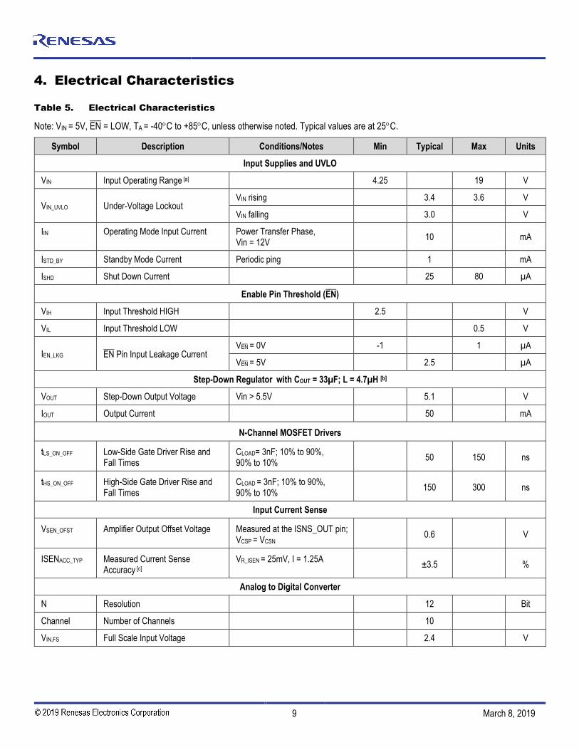
4. Electrical Characteristics
Table 5. Electrical Characteristics
Note: VIN = 5V, EN = LOW, TA = -40C to +85C, unless otherwise noted. Typical values are at 25C.
Symbol Description Conditions/Notes Min Typical Max Units
Input Supplies and UVLO
VIN Input Operating Range [a] 4.25 19 V
VIN_UVLO Under-Voltage Lockout VIN rising 3.4 3.6 V
VIN falling 3.0 V
IIN Operating Mode Input Current Power Transfer Phase, Vin = 12V
10 mA
ISTD_BY Standby Mode Current Periodic ping 1 mA
ISHD Shut Down Current 25 80 µA
Enable Pin Threshold (EN )
VIH Input Threshold HIGH 2.5 V
VIL Input Threshold LOW 0.5 V
IEN_LKG EN Pin Input Leakage CurrentVAEN¯¯ E A= 0V -1 1 µA
VAEN¯¯ E A= 5V 2.5 µA
Step-Down Regulator with COUT = 33µF; L = 4.7µH [b]
VOUT Step-Down Output Voltage Vin > 5.5V 5.1 V
IOUT Output Current 50 mA
N-Channel MOSFET Drivers
tLS_ON_OFF Low-Side Gate Driver Rise and Fall Times
CLOAD= 3nF; 10% to 90%, 90% to 10%
50 150 ns
tHS_ON_OFF High-Side Gate Driver Rise and Fall Times
CLOAD = 3nF; 10% to 90%, 90% to 10%
150 300 ns
Input Current Sense
VSEN_OFST Amplifier Output Offset Voltage Measured at the ISNS_OUT pin; VCSP = VCSN
0.6 V
ISENACC_TYP Measured Current Sense Accuracy [c]
VR_ISEN = 25mV, I = 1.25A ±3.5 %
Analog to Digital Converter
N Resolution 12 Bit
Channel Number of Channels 10
VIN,FS Full Scale Input Voltage 2.4 V

P9241-G Datasheet
© 2019 Integrated Device Technology, Inc. 10 March 8, 2019
Symbol Description Conditions/Notes Min Typical Max Units
LDO18 [b] (COUT = 1µF, VIN_LDO = 5.5V)
VLDO18 Output Voltage 1.8 V
VOUT/VOUT Output Voltage Accuracy -5 +5 %
IOUT18_MAX Maximum Output Current 20 25 mA
LDO33 [b] (COUT = 1µF, VIN_LDO = 5.5V)
VLDO33 COUT = 1µF, VVIN_LDO = 5.5V 3.15 3.3 3.45 V
VOUT/VOUT Output Voltage Accuracy -5 +5 %
IOUT18_MAX Maximum Output Current 10 25 mA
PREG
VPREG 5V LDO Regulator 5 V
Thermal Shutdown
TSD Thermal Shutdown Threshold rising 140 °C
Threshold falling 120 °C
Analog Input Pins Input Current Leakage (TS, VDEM1, VDEM2)
ILKG Leakage Current -1 1 µA
Open-Drain Pins Output Logic Levels (LED1, LED2, GPIO_A0, GPIO_A1)
VOH Output Logic HIGH 4 V
VOL Output Logic LOW I = 8mA 0.5 V
General Purpose Inputs/Outputs Pins Logic Levels
VIH Input Voltage HIGH Level 0.7 VDDIO V
VIL Input Voltage LOW Level 0.3 VDDIO V
ILKG Leakage Current 1 µA
VOH Output Logic HIGH I = 8mA, VDDIO = 3.3V 2.4 V
VOL Output Logic LOW I = 8mA, VDDIO = 3.3V 0.5 V
I2C Interface (GPIO_A0, GPIO_A1)
fSCL_SLV Clock Frequency As I2C slave 400 kHz
CB Capacitive Load For each bus line 100 pF
CBIN GPIO_A0, GPIO_A1 Input Capacitance
5 pF
ILKG Input Leakage Current V = GND and 3.3V -1 1 µA
[a] The input voltage operating range is dependent upon the type of transmitter power stage (full-bridge, half-bridge) and transmitting coil inductance.WPC specifications should be consulted for appropriate input voltage ranges by end-product type.
[b] Do not externally load. For internal biasing only.
[c] A 20mΩ, 1% or better sense resistor and 10Ω, 1% input filter resistors are required to meet the FOD specification.
P9241-G Datasheet
© 2019 Integrated Device Technology, Inc. 11 March 8, 2019
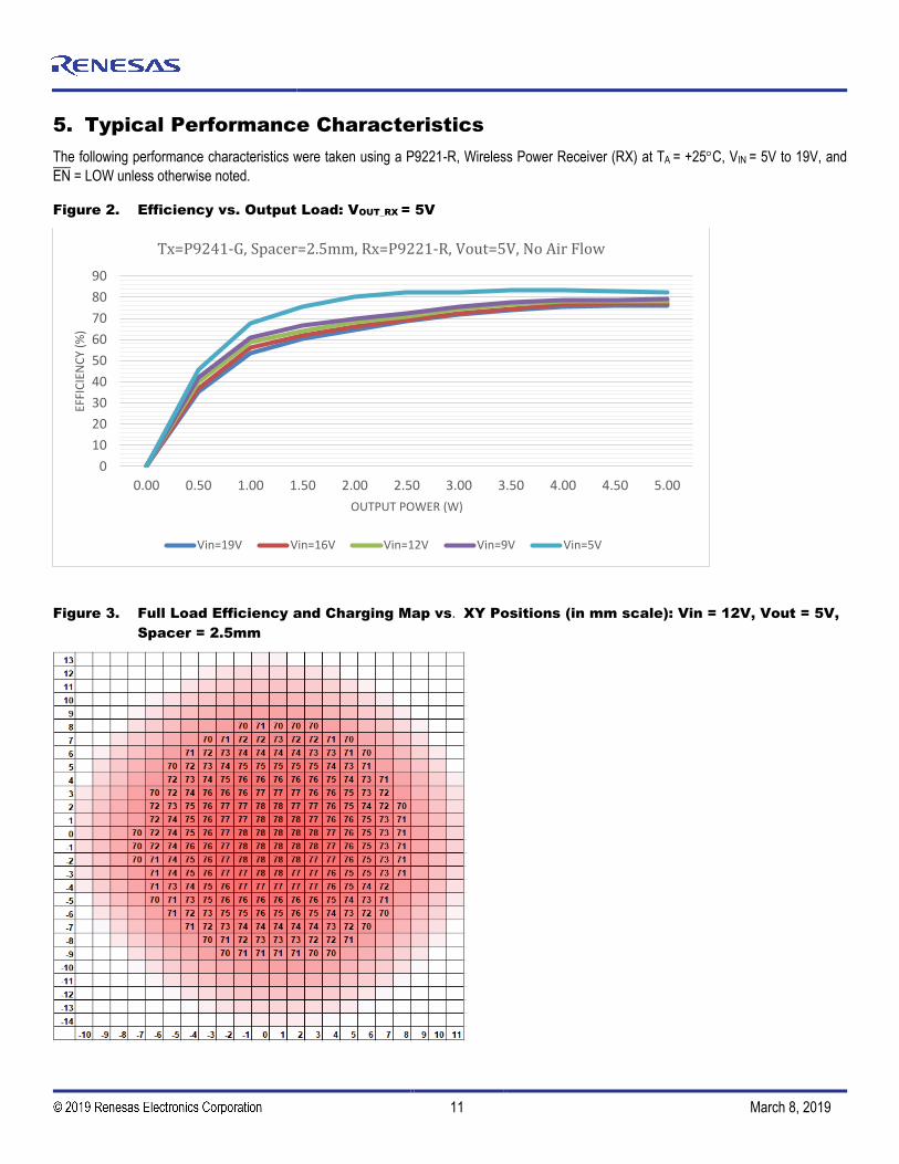
5. Typical Performance Characteristics
The following performance characteristics were taken using a P9221-R, Wireless Power Receiver (RX) at TA = +25C, VIN = 5V to 19V, and
EN = LOW unless otherwise noted.
Figure 2. Efficiency vs. Output Load: VOUT_RX = 5V
Figure 3. Full Load Efficiency and Charging Map vs. XY Positions (in mm scale): Vin = 12V, Vout = 5V,
Spacer = 2.5mm
0
10
20
30
40
50
60
70
80
90
0.00 0.50 1.00 1.50 2.00 2.50 3.00 3.50 4.00 4.50 5.00
EFFI
CIE
NC
Y (%
)
OUTPUT POWER (W)
Tx=P9241-G, Spacer=2.5mm, Rx=P9221-R, Vout=5V, No Air Flow
Vin=19V Vin=16V Vin=12V Vin=9V Vin=5V

P9241-G Datasheet
© 2019 Integrated Device Technology, Inc. 12 March 8, 2019
The following performance characteristics were taken using a P9221-R, Wireless Power Receiver (RX) at TA = +25C, VIN = 5V to 19V, and
EN = LOW unless otherwise noted.
Figure 4. Internal Buck Load Regulation
Figure 5. Load Regulation vs. Output Load: LDO33
4.9
5
5.1
5.2
5.3
0 10 20 30 40 50 60 70 80
VC
C_5
V [
V]
OUTPUT CURRENT[mA]
VCC_5V @85 C VCC_5V @25 C
VCC_5V @0 C VCC_5V @-40C
3.2
3.25
3.3
3.35
3.4
0 2 4 6 8 10 12 14 16 18 20 22 24 26 28 30
LO
D33
[V
]
OUTPUT CURRENT[mA]
LDO33 @85 C
LDO33 @25 C
LDO33 @0 C
LDO33 @-40 C

P9241-G Datasheet
© 2019 Integrated Device Technology, Inc. 13 March 8, 2019
The following performance characteristics were taken using a P9221-R, Wireless Power Receiver (RX) at TA = +25C, VIN = 5V to 19V, and
EN = LOW unless otherwise noted.
Figure 6. Load Regulation vs. Output Load: LDO18
Figure 7. Voltage and Current Signal for Demodulation: Ch2 = VSNS, Ch3 = ISNS_IN
1.7
1.75
1.8
1.85
1.9
0 2 4 6 8 10 12 14 16 18 20 22 24 26 28 30
LD
O18
[V
]
OUTPUT CURRENT[mA]
LOD18 @85 C
LOD18 @25 C
LOD18 @0C
LOD18 @-40 C

P9241-G Datasheet
© 2019 Integrated Device Technology, Inc. 14 March 8, 2019
The following performance characteristics were taken using a P9221-R, Wireless Power Receiver (RX) at TA = +25C, VIN = 5V to 19V, and
EN = LOW unless otherwise noted. Note: See the schematic in Figure 25 for the location of the signals in these figures.
Figure 8. USB Adaptor Start-up: Ch1 = VBRIDGE, Ch2 = Vin, Ch3 = D-, Ch4 = D+
Figure 9. 19V Fixed Voltage Adaptor Start-up: Ch1 = VBRIDGE, Ch2 = Vin, Ch3 = GPIO_B4, Ch4 = iIn

P9241-G Datasheet
© 2019 Integrated Device Technology, Inc. 15 March 8, 2019
VIN = 5V to 19V; EN = LOW. The following performance characteristics were taken using a P9221-R, Wireless Power Receiver (RX) at
TA = +25C unless otherwise noted. Note: See the schematic in Figure 25 for the location of the signals in these figures.
Figure 10. Enable and Disable of External Buck Regulator: Ch1 = VBRIDGE, Ch2 = Tx_SW, Ch3 = GPIO_B4

P9241-G Datasheet
© 2019 Integrated Device Technology, Inc. 16 March 8, 2019
6. Block Diagram
Figure 11. Block Diagram
0
Hal
f Brid
ge
Driv
ers
Con
trol
32-bit ARM
Processor
GPIO_A0
GPIO_A1
BST_BRG1
GH_BRG1
SW_BRG1
GL_BRG1
Hal
f Brid
ge
Driv
ers
Con
trol
BST_BRG2
GH_BRG2
SW_BRG2
GL_BRG2
PW
M G
ener
ator
and
FS
K M
odul
ator
CS
N
CS
P
+-
+
-
ISN
S_O
UT
IDE
MI
VD
EM
1
ASK
DecoderVBRG_IN
DRV_VIN
ISN
S
DATA
OTP
DATA
SRAM
I2C
VIN
5V
Buck
LDO33
PREG
LDO18
PREGSW_S
VIN_LDO
LDO33
LDO18
5V
3.3V
1.8V
GPIO_B8
GPIO_A7
USB
detect
GND2
LED1
LED2
OSC
TS
GPIO_A2
GPIO_A5
GPIO_A4
GPIO_A3
GN
D1
MUX
GPIO_B0
GPIO_B1
GPIO_B2
GPIO_B3
EP
VDDIO
I/O
Module
ISN
S
VIN
12 B
it
AD
C
GPIO_A6
EN
D-
D+
Crystal
Driver
GPIO_B5
GPIO_B6Ext. Clock Input
GP
IO_B
7
GP
IO_B
4
GND
GN
D3
VD
EM
2

P9241-G Datasheet
© 2019 Integrated Device Technology, Inc. 17 March 8, 2019
7. General Description
A wireless power charging system has a base station with one or more transmitters that make power available via DC-to-AC inverter(s) and transmit the power over a loosely-coupled inductor pair to a receiver in a mobile device. Before each transmitter and receiver pair starts transferring power, a power contract will be agreed upon and created by the RX and TX. The amount of power transferred to the mobile device is controlled by the wireless power receiver via sending communication packets to the transmitter to increase, decrease, or maintain the power level. If a fault is detected, the transmitter and receiver can also stop power transfer to protect the system. The communication packet from receiver to transmitter is purely digital and consists of logic 1s and 0s, which are added on top of the power link that exists between the transmitter (TX) and receiver (RX) coil. Amplitude shift keying (ASK) is used for the communication from receiver to transmitter; while communication from transmitter to receiver is achieved by frequency shift keying (FSK) modulation over the power signal frequency.
When the transmitter is not delivering power, it is in Standby Mode. The transmitter remains in Standby Mode and periodically pings until it detects the presence of a receiver. If a Baseline Power Profile (BPP) or Extended Power Profile (EPP) receiver is present, the transmitter can deliver up to 5W of output power.
The P9241-G has features that ensure a high level of functionality and compliance with the WPC V1.2.4 specification requirements as illustrated in Figure 14, including a power path that efficiently achieves power transfer, a simple and robust communication demodulation circuit, safety and protection circuits, configuration, and status indication circuits.
The P9241-G converges most popular wireless charging protocols including WPC Baseline Power Profile (BPP), up to 7.5W charging for iPhones and Android proprietary fast charging modes. Depending on the type and capability of the power supply, the P9241-G can operate in different modes. A USB adaptor detection circuit is also implemented in P9241-G by firmware. The P9241-G can detect input ports such as USB Standard Downstream Port (SDP), USB Charger Downstream Port (CDP), USB Dedicated Charging Port (DCP), and other AC/DC adaptors. When the connected power supply is limited at 5V, the P9241-G functions as a BPP transmitter and can deliver up to 5W at the Rx output.
The P9241-G supports constant and fixed frequency operation during power transfer. Under such application scenarios, the full-bridge input voltage is adjusted to control the P9241-G transmitted power, while its operating frequency is fixed at 127.7kHz. The accuracy depends on that of the external clock or oscillator. If the IDT’s clock IC is used, the accuracy of the operating frequency is guaranteed at 127.7kHz ±6Hz. When using the Fixed-Frequency Operation Mode, an external step-down converter is employed in the P9241-G reference design to control the input voltage of the full-bridge inverter. Thus, the output of the step-down buck regulator is connected to the input of the P9241-G full-bridge inverter. A PWM signal from the P9241-G is used to control the output of the buck regulator by adjusting its duty ratio. To respond to an increase or decrease in the power request from receiver, the P9241-G regulates the duty ratio of the PWM signal accordingly.

P9241-G Datasheet
© 2019 Integrated Device Technology, Inc. 18 March 8, 2019
8. WPC Mode Characteristics
The WPC-1.2.4 baseline power profile (BPP) wireless power specification has a Selection Phase, Ping Phase, Identification and Configuration Phase, and Power Transfer Phase as shown in Figure 14.
Figure 12. WPC Power Transfer Phases Flowchart
Ping
Identification and
Configuration
Power Transfer
Selection
Extend Digital Ping
Power Transfer Contract Established
Apply Power Signal
No Response
Power Transfer Complete
Abort Digital Ping
No Power Transfer Contract
Unexpected Packet
Transmission Error
Timeout
Power Transfer Contract Violation
Unexpected Packet
Timeout
8.1 Selection Phase
In the Selection Phase, the power transmitter determines if it will proceed to the Ping Phase after detecting the placement of an object. In this phase, the power transmitter typically monitors the interface surface for the placement and removal of objects using a measurement signal. This measurement signal is low level in order to not wake up a power receiver if it is positioned on the interface surface.
8.2 Ping Phase (Digital Ping)
In the Ping Phase, the power transmitter will start transmitting a power signal and will also detect the response from a possible power receiver. This response ensures that the power transmitter is linking to a power receiver rather than to some unknown object. When a WPC-compatible power receiver is placed on a WPC-compatible charging pad, it responds to the power signal by rectifying the power signal. When the receiver’s internal bias voltage is greater than a specific threshold level, then the receiver is initiated, enabling the WPC communication protocol. If the power transmitter correctly receives a signal strength packet, the power transmitter proceeds to the Identification and Configuration Phase, maintaining the power signal output to the receiver.

P9241-G Datasheet
© 2019 Integrated Device Technology, Inc. 19 March 8, 2019
8.3 Identification and Configuration Phase
This protocol extends the digital ping in order to enable the power receiver to communicate the relevant information in the Identification and Configuration Phase. The Identification and Configuration Phase is part of the WPC protocol so that the power transmitter and power receiver establish an initial default power transfer contract.
In the Configuration Phase, the power transmitter and receiver exchange information for a default power transfer contract as follows:
The power transmitter receives the configuration packet.
If the power transmitter does not acknowledge the request (does not transmit FSK modulation), power receiver will assume a BPPtransmitter is present.
8.4 Power Transfer Phase
In this phase, the power transmitter and power receiver control the power transfer by means of the following packets:
Control Error Packets (CEP)
Received Power Packet (RPP, FOD-related)
End Power Transfer (EPT) Packet
Once a power contract is established, the transmitter initiates the Power Transfer Phase. The receiver’s control and communication circuit sends control error packets to the transmitter to adjust the rectifier voltage to the level required to maximize the efficiency of the linear regulator, and to send to the transmitter the actual received power packet for foreign-object detection (FOD) to guarantee safe, efficient power transfer.
In the event of an EPT issued by the receiving device, the receiver will send an EPT packet to the transmitter and the transmitter can terminate the existing power transfer.

P9241-G Datasheet
© 2019 Integrated Device Technology, Inc. 20 March 8, 2019
9. Application Information
9.1 Internal Power Supply and Internal Bias
The P9241-G has integrated internal buck regulators and internal LDOs to provide internal power.
9.1.1 Integrated Step-Down Regulator
To provide a power supply for the P9241-G internal circuitry as well as to reduce the power loss from a wide input voltage range, a step-down buck regulator is integrated. It is internally compensated for the convenience of design. It takes the power from the input voltage to the P9241-G and regulates the DC voltage to 5V for use as an internal VCC_5V supply.
The internal step-down regulator supplies the power to the integrated MOSFET driver circuits, the internal LDO18, and the LDO33 linear regulators. It must not be used to power any external load.
9.1.2 Linear Regulators – PREG, LDO33, and LDO18
The P9241-G has three low-dropout (LDO) regulators. The 5V pre-regulator (PREG) provides voltage for the internal bias. The PREG requires a 1μF ceramic bypass capacitor connected from the PREG pin to GND. This capacitor must be placed very close to the PREG pin. The PREG voltage regulator must not be externally loaded.
The LDO33 and LDO18 are used to bias the internal analog and digital circuit. The regulator’s input voltage is supplied through the VIN_LDO pin. Both regulators require a 1μF ceramic capacitor from the pin to GND. Both the LDO18 and LDO33 regulators must not be externally loaded.
9.2 Enable Pin
The P9241-G device can be disabled by applying a logic HIGH to the EN pin. When the voltage on the EN pin is pulled HIGH, operation is
suspended and the P9241-G is placed into the low-current Shut-Down Mode. If EN is pulled LOW, the P9241-G is enabled and active. The
rising and falling threshold for the EN is specified in Table 5.
9.3 Software Under-Voltage Lock-Out (UVLO) Protection
The P9241-G has software UVLO features that protect the adaptor input port from being overloaded. For different adaptor voltages that are established, different UVLO levels are implemented. To guarantee proper functionality, the voltage on the VIN pin must be above the UVLO threshold. If the input voltage stays below the UVLO threshold, the P9241-G shuts down the system. If a software UVLO is triggered more than three times in a row, then the P9241-G will shut down, as an identified fault condition.
Figure 13. UVLO Threshold Definition
Shut-Down
Mode
Shut-Down
Mode
Normal Operating
Mode
Time
VIN_UVLO_RISING
VIN
[V]
VIN_UVLO_FALLING

P9241-G Datasheet
© 2019 Integrated Device Technology, Inc. 21 March 8, 2019
9.4 Die Temperature Protection
The P9241-G integrates die thermal shutdown circuitry to prevent damage resulting from excessive thermal stress that may be encountered under fault conditions. This circuitry will shut down or reset the P9241-G if the die temperature exceeds the threshold to prevent damage resulting from excessive thermal stress. An internal temperature protection block is enabled in the P9241-G that monitors the temperature inside the chip.
If the die temperature exceeds 140°C, the P9241-G shuts down and resumes when the internal temperature drops below 120°C.
9.5 External Temperature Sensing – TS
The P9241-G has a remote temperature sensor input, TS, which can be used to monitor an external temperature by using a thermistor. The built-in comparator’s reference voltage is 0.6V with a 0.8V recovery voltage. Figure 16 shows the temperature sensor circuits. Specific values for the thermistor and associated components are shown in Figure 25. Specific thermistor characteristics are included in the thermistor manufacturer’s datasheet.
Figure 14. NTC Thermistor Connection to the TS Pin
LDO33
TS
P9241-G
ADC
To disable the thermistor, connect the TS pin to the LDO33 pin. Do not leave the TS pin floating.
9.6 Full-Bridge Driver
The transmitter switching frequency and duty cycle are controlled by the two groups of half-bridge drivers with bootstrap diodes that have been integrated into the P9241-G. Each driver can drive a half bridge of two N-channel MOSFETs. The dead-time of each half-bridge can be set in the firmware to guarantee zero voltage switching as well as no risk of shoot-through. Each half-bridge driver can be controlled separately in the firmware, and thus the phase-shifted full-bridge or half-bridge can be enabled through the firmware.
The internal buck regulator provides 5V to both groups of half bridge driver circuits through the DRV_VIN pin. Applying any extra load on the internal buck regulator output is not recommended, since any extra load will compromise its loading capability and noise might be coupled into the half-bridge drivers.
9.7 LC Resonant Circuits
The LC resonant tank comprises a primary resonant coil (LP) and series resonant capacitance (CP). The LC resonant tank provides a resonant frequency at which it offers the minimum series resistance across the LC tank. The full-bridge or half-bridge inverter circuit drives the LC tank and operates above the LC resonant frequency to guarantee zero voltage switching at the transmitter side. The WPC-based transmitter is not specified to operate at the resonant frequency at any time.

P9241-G Datasheet
© 2019 Integrated Device Technology, Inc. 22 March 8, 2019
The P9241-G is designed to support various Baseline Power Profile (BPP) coil configurations using half-bridge and full-bridge inverter topologies to drive the primary coil (LP) and series resonant capacitors (CP). Depending on the WPC coil configuration and specification, the coil inductance and series capacitance value can vary in a wide range. The transmitter coil specification must comply with the WPC definition. The WPC specification defines the transmitter coil self-inductance value, DC resistance (DCR), form factor, size, and number of turns. For the BPP coil configurations, A11 and A5 are supported by the P9241-G. For each WPC-specified transmitter coil configuration, the required resonant capacitance is also defined. High-voltage-rated, multi-layer ceramic capacitors that feature stable AC and DC characteristics (such as the C0G type) and stable temperature characteristics are highly recommended for this application.
9.8 WPC Communication Interface
9.8.1 Modulation/Communication
The WPC specification uses two-way communication for power transfer: receiver-to-transmitter and transmitter-to receiver.
Receiver-to-transmitter communication is completed by modulating the load applied to the receiver’s coil; the communication is purely digital and logic 1s and 0s are modulated onto the power transfer signal waveform. Modulation is done with amplitude-shift keying (ASK) modulation with a bit-rate of 2Kbps. To the transmitter, this appears as an impedance change, which results in measurable variations of the transmitter’s coil. The power transmitter demodulates this variation of the coil voltage to receive the packets.
Transmitter-to-receiver communication is accomplished by frequency-shift keying (FSK) modulation over the power signal frequency. The power transmitter P9241-G can modulate FSK data onto the power transfer signal frequency and use it in order to establish the handshaking protocol with the power receiver.
Figure 15. Example of Differential Bi-phase Encoding for FSK
tCLK = 256/fOP
ONE ZERO ONE ZERO ONE ONE ZERO ZERO
512 Cycles 256 Cycles
Each byte will comply with the start, data, parity, and stop asynchronous serial format structure shown in Figure 18:
Figure 16. Example of Asynchronous Serial Byte Format for FSK
Start StopParityb0 1 2 3 4 5 6 7b b b b b b b

P9241-G Datasheet
© 2019 Integrated Device Technology, Inc. 23 March 8, 2019
9.8.2 Bit Decoding Scheme for ASK
As required by the WPC specification, the P9241-G uses a differential bi-phase coding scheme to demodulate the data bits from the power transfer signal. A frequency of 2kHz is used for this purpose. A logic ONE bit is coded using two narrow transitions; a logic ZERO bit is encoded using one wider transition as shown in Figure 19.
Figure 17. Bit Decoding Scheme
t CLK
ONE ZERO ONE ZERO ONE ONE ZERO ZERO
Each byte in the communication packet comprises 11 bits in an asynchronous serial format, as shown in Figure 20.
Figure 18. Byte Decoding Scheme
Start StopParityb0 1 2 3 4 5 6 7b b b b b b b
Each byte has a start bit, 8 data bits, a parity bit, and a single stop bit.
Each ASK communication packet has the following structure as shown in Figure 21.
Figure 19. Communication Packet Structure
Preamble Header Message Checksum
9.8.3 ASK Voltage Demodulation – VDEM1 Pin
In order to improve WPC ASK communication reliability under all loading conditions, the P9241-G has integrated two demodulation schemes: one based on input current information and the other based on coil voltage information. During the ASK communication initialed by the receiver, the envelope of the transmitter coil voltage reflects the ASK communication packet. The communication packet can be received by tracking the envelope of the coil voltage.
The voltage mode envelope detector is implemented using a combination of an RC-based filter as displayed in Figure 22. This simple implementation achieves the envelope detector function by combining a low-pass filter as well as a DC rejection filter.
Figure 20. Voltage Mode Envelope Detector
Coil Voltage
(VCOIL)
Packet
DecoderTo
Registers
P9241-G
VDEM1
ASK Decoder

P9241-G Datasheet
© 2019 Integrated Device Technology, Inc. 24 March 8, 2019
The filtered signal from the transmitter coil voltage will be processed by the P9241-G internal ASK decoder circuit, which includes an operational amplifier to automatically condition the filtered signals, and then a digital packet decoder to translate the signal into communication packets.
9.8.4 ASK Current Demodulation – IDEMI Pin
The ASK current demodulation scheme receives input current information from the current sense resistor, which carries the coil current modulation information on top of the averaged input current as shown in Figure 23. Similar to voltage demodulation circuits, an external discrete low-pass filter and DC filter between the ISNS_OUT and IDEMI pins provide additional filtering.
The packet decoder block is shared between the voltage and current detectors. The packet decoder selects either voltage information or current information from the filtered signals, depending upon which produces the better demodulated signal.
Figure 21. Current Mode Envelope Detector
CS
P
CS
N
VIN Vbridge
ISN
S_O
UT
IDE
MI
Packet
DecoderTo
Registers
20m
P9241-G ASK Decoder
9.9 General Purpose Input/output – GPIO Pins
The P9241-G has 11 GPIOs, some of which can be repurposed in the firmware to perform functions such as setting and changing the LED patterns, etc.
9.9.1 Input Port Detection and Receiver Support – GPIO_A5, GPIO_A7, and GPIO_B8
The P9241-G supports input voltages in a wide range, such as a 5V, 9V, 12V, and 16V to 19V fixed DC power supply. Depending on the reference design and WPC coil configuration selection, the P9241-G can support a variety of receivers based on the input voltage as shown in Table 6.
When an AC/DC adaptor is connected to the P9241-G, it will detect if this is a USB port, based on the D+ and D- signals. In the case that a USB port is detected, the P9241-G will identify the type of USB port by executing the USB Battery Charging (BC 1.2) protocol on the D+ and D- signals. The P9241-G can adjust the input voltage to the highest level possible that enables as many receiver types as possible, as shownin Table 6. The GPIO_A5 and GPIO_A7 pins are used for D- detection and communication; GPIO_B8 is used for D+ detection andcommunication.
If the AC/DC adaptor is connected through a DC barrel jack or a fixed DC voltage, the P9241-G will set up the operation mode and support the corresponding receivers listed in Table 6.
When the DC source is 5V fixed, the P9241-G operates in the BPP mode only and supports up to 5W. In this operation mode, the P9241-G disables the external power-stage buck regulator and enables an external MOSFET to bypass the buck regulator.

P9241-G Datasheet
© 2019 Integrated Device Technology, Inc. 25 March 8, 2019
Table 6. Input Voltage vs. Receiver Supported
Input Voltage/Current Rating Receiver Supported
5V/2A BPP (Bypass External Buck Regulator)
9V/1.67A
BPP 5W
Up to 8W charging for Android Phones
Up to 7.5W charging for iOS iPhones
12V/2A
BPP 5W
Up to 10W charging for Android Phones.
Samsung AFC
Up to 7.5W charging for iOS iPhones
16V to 19V/1.8A
BPP 5W
Up to 10W charging for Android Phones.
Samsung AFC
Up to 7.5W charging for iOS iPhones
9.9.2 Foreign Object Detection – GPIO_A3
When metallic objects, such as coins, keys, and paperclips, are exposed to alternating magnetic fields, the eddy current flowing through such objects will cause a power loss and the metallic object will exhibit a temperature increase. The amount of heat generated is a function of the strength and frequency of the magnetic field, as well as the characteristics of the object, such as resistivity, size, and shape. In a WPC-based wireless power system, the heat generated by the eddy current manifests itself as a power loss reducing the overall system efficiency. If appropriate actions are not taken, the heating could lead to unsafe conditions.
9.9.2.1 Power Difference in the Power Transfer Phase – GPIO_A3
The foreign object detection is achieved during the Power Transfer Phase. The power loss is calculated between the reported received power and the transmitted power, which is constantly measured and compared with the WPC-specified thresholds. In normal power transfers, the power difference between received power and transmitted power (power loss) is constantly lower than the pre-set threshold. However, if a foreign object has been placed on its surface and is able to be coupled with the magnetic flux, this can generate additional power loss, which can become significantly large. If the loss is higher than the threshold set by the WPC specification, the power loss FOD protection mechanism will be triggered and the transmitter will shut down the whole system to avoid overheating and a potentially unsafe situation.
The power loss can be different based on the component selection, PCB layout, and end-product casing. Therefore, it must be adjusted according to each design. The P9241-G has a set of default power-loss FOD thresholds loaded in the firmware. It can be modified based on the voltage across GPIO_A3 as shown in Table 7.
Note: GPIO_A3 is a multi-function pin, which is also used to set the LED pattern (for LED pattern settings, see LED Pattern Selection – GPIO_A3.

P9241-G Datasheet
© 2019 Integrated Device Technology, Inc. 26 March 8, 2019
Table 7. Voltage on GPIO_A3 vs. FOD Threshold
Note: Do not set the GPIO_A3 voltage close to the endpoints of the selected range.
Voltage on GPIO_A3 (V) Power Difference FOD Threshold
0V ≤ VGPIO_A3 < 0.7V Default values
0.7V < VGPIO_A3 <1.4V 2 × default values
1.4V < VGPIO_A3 < 2.1V 3 × default values
2.1V < VGPIO_A3 < 2.4V 4 × default values
9.9.3 Control of External Power Stage DC/DC Buck Regulator – GPIO_B4 and GPIO_B7
To regulate the receiver output voltage, as well as to regulate the system’s delivered power, the transmitter adjusts the DC/AC inverter switching frequency, duty cycle, or DC/AC inverter input voltage. For the WPC coil configurations that operate at a fixed frequency and require adjusting the inverter bridge input voltage, the P9241-G supports these coil configurations by employing an external front-end DC/DC stage. The external DC/DC is part of the power stage, which connects between the input voltage and the DC/AC inverter.
For Apple 7.5W charging mode, the P9241-G supports fixed and precise switching frequency at 127.7kHz, and thus its bridge input voltage must be adjusted. Another stage of the external buck regulator is added to regulate the input voltage of the full bridge LC circuits. GPIO_B4 is used to enable/disable this external DC/DC buck regulator. GPIO_B7 generates a PWM signal that is applied on top of the feedback pin of the buck regulator through a low-pass filter to fine-tune the output voltage of the buck regulator. The resolution of the buck regulator output depends on the buck IC’s internal reference voltage, output voltage range, buck regulator compensation design, and resolution of the PWM signal from GPIO_B7.
9.9.4 Bypass External DC/DC Buck Regulator– GPIO_A4
When the input voltage is 5V only, the P9241-G operates in BPP mode to support legacy adaptors, as shown in Table 6. However, enabling the external power stage buck regulator at this time compromises the efficiency, thermal performance, and maximum power that can be delivered to the receiver. Under such an application scenario, the P9241-G will disable the external power stage buck regulator and enable another power path for the input voltage (5V) to be directly applied to the DC/AC inverter. GPIO_A4 is used to bypass the external power stage buck regulator. In this mode, the P9241-G operates in a mode for a fixed input voltage with variable frequency. The operating frequency range depends on the WPC coil configuration specification.
9.9.5 Coil Over-Voltage Control – GPIO_A6
The voltage across the transmitter coil can be excessive as the bridge input and frequency changes. Some unprotected receivers might risk being damaged or malfunction if placed on top of the transmitter coil immediately after another receiver is removed. When the voltage across the transmitter coil is too high, the P9241-G will open an additional switch via GPIO_A6 and cause a reduction in the coil voltage.
9.9.6 External Oscillator– GPIO_B5 and GPIO_B6
To guarantee that the operating frequency is precisely at 127.7kHz within a tolerance of ±50ppm under different temperature conditions, the P9241-G requires an external oscillator to provide accurate frequency operation. The PLL and crystal driver circuits inside the P9241-G guarantee that the internal clock for the ARM Cortex-M0 core is synchronized with the external oscillator frequency.
GPIO_B6 is used as the external oscillator frequency synchronization input. Either a clock IC or another oscillator can be used to generate 6.16791MHz. GPIO_B5 must connected to GND and cannot be used for other applications if GPIO_B6 is used as the external frequency synchronization pin.

P9241-G Datasheet
© 2019 Integrated Device Technology, Inc. 27 March 8, 2019
9.9.7 LED Pattern Selection – GPIO_A3
The P9241-G uses two LED outputs to indicate the power transfer status, faults, and operating modes depending on the voltage level on the GPIO_A3 pin. The GPIO_A3 pin also programs the power difference FOD thresholds (see Power Difference in the Power Transfer Phase – GPIO_A3. The LEDs are connected to the LED1 and LED2 pins as shown in the typical application schematic in Figure 25. The LED pattern can be selected using the external resistor divider based on Table 8.
Table 8. Resistors for Setting the LED Pattern
Note: Do not set the GPIO_A3 voltage close to the endpoints of the selected range.
Option Voltage on GPIO_A3 Pin LED1/LED2 Pin
Status
Standby Transfer Complete Fault
1
0V ≤ VGPIO_A3 < 0.1V;
0.7V < VGPIO_A3 < 0.8V;
1.4V < VGPIO_A3 < 1.5V;
2.1V < VGPIO_A3 < 2.4V
LED2 Off On Off Off
LED1 Off Off Off Blink 4Hz
2
0.1V < VGPIO_A3 < 0.2V;
0.8V < VGPIO_A3 < 0.9V;
1.5 V< VGPIO_A3 < 1.6V
LED2 On On Off Off
LED1 On Off Off Blink 4Hz
3
0.2V < VGPIO_A3 < 0.3V;
0.9V < VGPIO_A3 < 1.0V;
1.6V < VGPIO_A3 < 1.7V
LED2 Off Blink 1Hz On Blink 4Hz
LED1 Off Off Off Off
4
0.3V < VGPIO_A3 < 0.4V;
1.0V < VGPIO_A3 < 1.1V;
1.7V < VGPIO_A3 < 1.8V
LED2 Off On Off Blink 4Hz
LED1 Off Off Off Off
5
0.4V < VGPIO_A3 < 0.5V;
1.1V < VGPIO_A3 < 1.2V;
1.8V < VGPIO_A3 < 1.9V
LED2 On Blink 1Hz On Off
LED1 On Off Off Blink 4Hz
6
0.5V < VGPIO_A3 < 0.6V;
1.2V < VGPIO_A3 < 1.3V;
1.9V < VGPIO_A3 < 2.0V
LED2 Off Off On Off
LED1 Off On Off Blink 4Hz
7
0.6V < VGPIO_A3 < 0.7V;
1.3V < VGPIO_A3 < 1.4V;
2.0V < VGPIO_A3 < 2.1V
LED2 Off Blink 1Hz On Off
LED1 Off Off Off Blink 4Hz

P9241-G Datasheet
© 2019 Integrated Device Technology, Inc. 28 March 8, 2019
9.9.8 I2C Communication Interface – GPIO_A0 and GPIO_A1
The P9241-G supports the standard I2C interface. The default I2C slave address is 61HEX. GPIO_A0 serves as the I2C clock line, and GPIO_A1 serves as the I2C data line. Figure 24 shows the READ and WRITE protocol structure that the external I2C master must use to communicate with the P9241-G.
Figure 22. I2C Access Read Protocol and Write Protocol
From Master
From Slave
ACK ACK ACK
DataByte_1 A A DataByte_3 A
8 1 8 1 8 1
ACK
DataByte_0 A
8 1Clocks
. . . .DataByte_2
Start 61HEX 61HEXACK 06HEX ACK 80HEX ACK ACKR/W R/W
S Slave Address Sr Slave AddressAMemory Address
MSB0 A
Memory Address
LSBA 1 A . . . .
1 7 71 8 1 8 1 11 1Clocks
Read Protocol
P
ACK ACK
CmdByte_1 A A CmdFlag_1
8 1 8 1 8 1
ACK
CmdByte_0 A
8 1Clocks
CmdFlag_0 A/A
1
NAK
LSB = Least Significant Byte
MSB = Most Significant Byte
A = Acknowledge (SDA LOW)
A = Not Acknowledge (SDA HIGH)
S = Start Condition
Sr = Restart Condition
P = Stop Condition
From Master
From Slave
ACK ACK ACK
DataByte_1 A A DataByte_3 A
8 1 8 1 8 1
ACK
DataByte_0 A
8 1Clocks
. . . .DataByte_2
Write Protocol
P
ACK ACK
CmdByte_1 A A CmdFlag_1
8 1 8 1 8 1
ACK
CmdByte_0 A
8 1Clocks
CmdFlag_0 A/A
1
NAK
Start 61HEX ACK 06HEX ACK 80HEX ACKR/W
S Slave Address AMemory Address
MSB0 A
Memory Address
LSBA . . . .
1 7 1 8 1 8 11Clocks
LSB = Least Significant Byte
MSB = Most Significant Byte
A = Acknowledge (SDA LOW)
A = Not Acknowledge (SDA HIGH)
S = Start Condition
Sr = Restart Condition
P = Stop Condition

P9241-G Datasheet
© 2019 Integrated Device Technology, Inc. 29 March 8, 2019
9.9.9 External Memory – GPIO_B0, GPIO_B1, GPIO_B2, and GPIO_B3
The P9241-G requires an external flash memory in which the firmware must be programmed during the development stage. The P9241-G accesses external flash memory using the SPI interface to upload the firmware into the internal SRAM. The Winbond W25X20CLUXIG is the recommended external flash memory.
The GPIO_B0, GPIO_B1, GPIO_B2, and GPIO_B3 pins are used for the external flash memory read and write.
10. Register Addresses and Definitions
The tables in this section provide a comprehensive list of address locations, field names, available operations (R or RW), default values, and functional descriptions of all internally accessible registers in the P9241-G. The default I2C slave address is 61HEX. The address of each register is 16 bits. Note that some values require multiple registers and therefore span multiple addresses. For example, the address of the device ID high byte is 0001HEX and the low byte address is 0000HEX.
Table 9. Read Register – Device ID Register
Address and Bit Register Field Name R/W Default Function and Description
0000HEX Device_ID [7:0] R 42HEX Device ID low byte
0001HEX Device_ID [15:8] R 92HEX Device ID high byte
Table 10. Read Register – Firmware Revision
Address and Bit Register Field Name R/W Default Function and Description
00004HEX FW_Major_Rev [7:0] R 18HEX Major firmware revision low byte
00005HEX FW_Major_Rev [15:8] R 00HEX Major firmware revision high byte
00006HEX FW_Rev [7:0] R 01HEX Project code firmware version
00007HEX FW_Rev [15:8] R 00HEX Customer code firmware version
Table 11. Read Register – State Register
Address and Bits Register Field Name R/W Default Function and Description
0707HEX System State R -
0DEC = Detection Phase
1DEC = Selection Phase
2DEC = Ping Phase
3DEC = ID Phase
5DEC = Configuration Phase
6DEC = Not Used
7DEC = Not Used
8DEC = Power Transfer Phase
9 DEC = Renegotiation Phase
10DEC = Remove Power

P9241-G Datasheet
© 2019 Integrated Device Technology, Inc. 30 March 8, 2019
Table 12. Read Register – Error Code Register
Address and Bits Register Field Name R/W Default Function and Description
0614HEX System Error [7:0] R 00HEX
Bit 0 = End Power Transfer command from receiver
Bit 6 = Signal strength
Bit 7 = WPC packager timeout
0615HEX System Error [15:8] R 00HEX Bit 0 = Control Error Packet timeout
Bit 1 = Received Power Packet timeout
Bit 2 = Over-current protection during the Digital Ping Phase
Bit 3 = Over-voltage
Bit 4 = Under-voltage
Bit 5 = FOD in power transfer
Bit 6 = Over-temperature
0616HEX System Error [23:16] R 00HEX Bit 1 = Over-current
Bit 5 = Buck error
Bit 6 = Not Used
Table 13. Read Register – Adaptor Type Register
Address and Bits Register Field Name R/W Default Function and Description
070EHEX Adaptor Type R -
0DEC = None
1DEC = USB SDP
2DEC = USB DCP
3DEC = USB CDP
4DEC = QC 2.0
5DEC = Other QC
12DEC = Adaptor detect error
Table 14. Read Register – Potential Power Register
Address and Bits Register Field Name R/W Default Function and Description
083EHEX Potential_Power R – Transmitter potential power in W.
Table 15. Read Register – Input Current
Address and Bits Register Field Name R/W Default Function and Description
0664HEX Bridge_input_current [7:0] R – LSB of input current value in mA.
0665HEX Bridge_input_current [15:8] R – MSB of input current value in mA.

P9241-G Datasheet
© 2019 Integrated Device Technology, Inc. 31 March 8, 2019
Table 16. Read Register – Input Voltage
Address and Bits Register Field Name R/W Default Function and Description
0668HEX Input_voltage [7:0] R – LSB of coil voltage value in mV.
0669HEX Input_voltage [15:8] R – MSB of coil voltage value in mV.
Table 17. Read Register – Remote Temperature Sensing Voltage
Address and Bits Register Field Name R/W Default Function and Description
06A4HEX Thermistor pin voltage [7:0] R – LSB of thermistor voltage value.
06A5HEX Thermistor pin voltage [15:8] R – MSB of thermistor voltage value.
Table 18. Read Register – Operating Frequency
fOP = 61.6791MHz
FRE_CNT[15:0] + 2
Address and Bits Register Field Name R/W Default Function and Description
0632HEX FRE_CNT [7:0] R – LSB of operating frequency count.
0633HEX FRQ_CNT [15:8] R – MSB of operating frequency count.
Table 19. Read Register – Transmitter Duty Cycle
D = FRE_CNT[7:0]
511
Address and Bits Register Field Name R/W Default Function and Description
05CFHEX Transmitter_Duty R – Transmitter duty cycle.
Table 20. Read Register – Transmitter Power 32 Bit
Address and Bits Register Field Name R/W Default Function and Description
0880HEX Tx_Power [7:0] R – LSB of transmitter power, low byte in mW
0881HEX Tx_Power [15:8] R – MSB of transmitter power, low byte in mW
0882HEX Tx_Power [23:16] R – LSB of transmitter power, high byte in mW
0883HEX Tx_Power [31:24] R – MSB of transmitter power, high byte in mW
P9241-G Datasheet
© 2019 Integrated Device Technology, Inc. 32 March 8, 2019
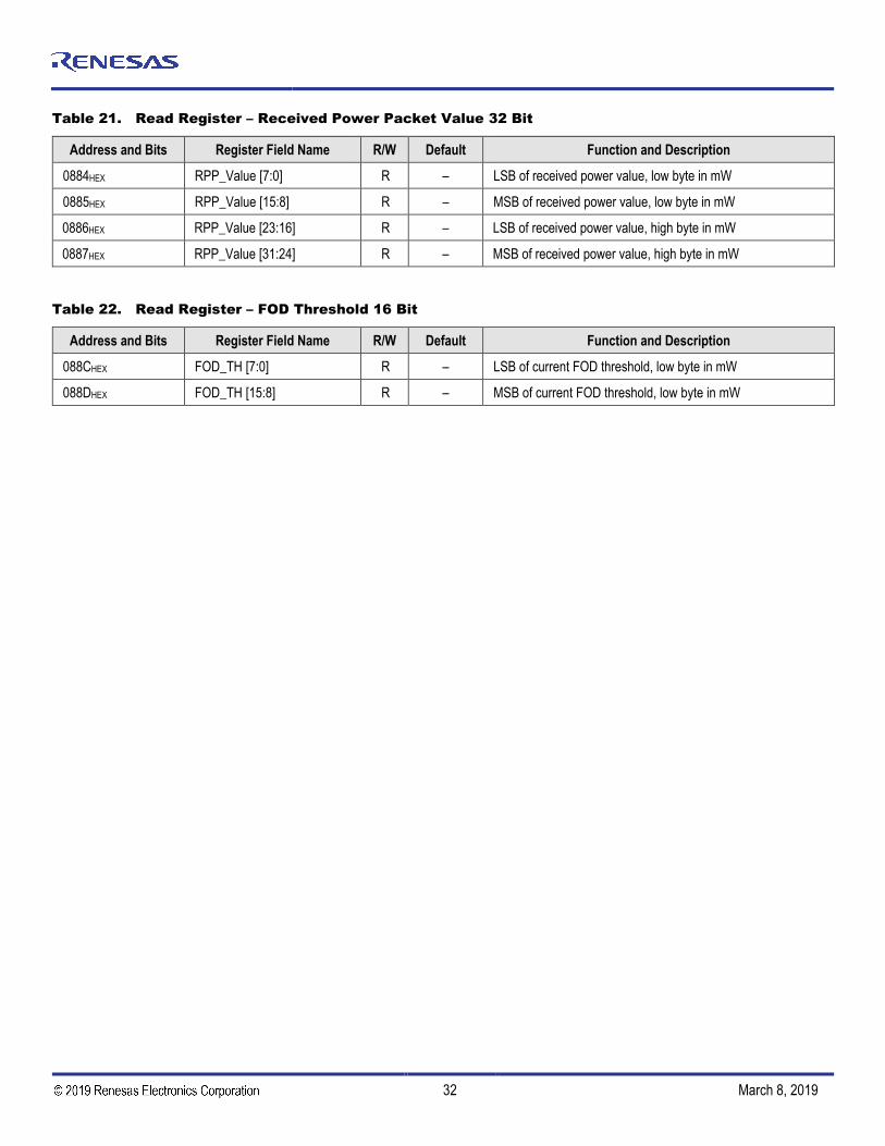
Table 21. Read Register – Received Power Packet Value 32 Bit
Address and Bits Register Field Name R/W Default Function and Description
0884HEX RPP_Value [7:0] R – LSB of received power value, low byte in mW
0885HEX RPP_Value [15:8] R – MSB of received power value, low byte in mW
0886HEX RPP_Value [23:16] R – LSB of received power value, high byte in mW
0887HEX RPP_Value [31:24] R – MSB of received power value, high byte in mW
Table 22. Read Register – FOD Threshold 16 Bit
Address and Bits Register Field Name R/W Default Function and Description
088CHEX FOD_TH [7:0] R – LSB of current FOD threshold, low byte in mW
088DHEX FOD_TH [15:8] R – MSB of current FOD threshold, low byte in mW

P9241-G Datasheet
© 2019 Integrated Device Technology, Inc. 33 March 8, 2019
11. Power Dissipation and Thermal Requirements
The P9241-G is offered in a 48-VFQFPN package that has a maximum power dissipation capability of approximately 1.47W. The maximum power dissipation of the package is determined by the number of thermal vias between the package and the printed circuit board (PCB), and is defined by the die’s specified maximum operating junction temperature, TJ(MAX) of 125°C. The junction temperature rises when the heat generated by the device’s power dissipation flow is impeded by the package-to-PCB thermal resistance.
The VFQFPN package offers a typical thermal resistance, junction to ambient (θJA), of 27.2°C/W when the PCB layout design is optimized as described in the P9241-G Layout Guide. The techniques noted in the PCB layout section must be followed when designing the PCB layout. Take into consideration possible proximity to other heat-generating devices when placing the P9241-G and the bridge FET packages in a given application design. The ambient temperature around the power IC will also affect the thermal limits of an application. The main factors influencing θJA (in the order of decreasing influence) are PCB characteristics, the size of the thermal pad attached to the die/package (VFQFPN), the thermal vias, and the final system hardware construction. Board designers should keep in mind that the package thermal metric θJA is impacted by the characteristics of the PCB. Changing the design or configuration of the PCB changes the overall thermal resistivity and the board’s heat-sinking efficiency.
Three basic approaches for enhancing thermal performance include:
Improving the power dissipation capability of the PCB design
Improving the thermal coupling of the component to the PCB
Introducing airflow into the system
First, the maximum power dissipation for a given situation should be calculated using Equation 1:
PD(MAX) =(TJ(MAX) – TAMB)
θJA
Equation 1
Where: PD(MAX) = Maximum power dissipation
θJA = Package thermal resistance (°C/W)
TJ(MAX) = Maximum device junction temperature (°C)
TAMB = Ambient temperature (°C)
The maximum recommended operating junction temperature (TJ(MAX)) for the P9241-G is 125°C. The thermal resistance of the 48-VFQFPN package is optimally θJA = 27.2°C/W. Operation is specified to a maximum steady-state ambient temperature (TAMB) of 85°C. Therefore, the maximum recommended power dissipation is given by Equation 2.
PD(MAX) =(125 – 85)
27.2/W≅ 1.47W
Equation 2
All the previously mentioned thermal resistances are the values found when the P9241-G is mounted on a standard board of the dimensions and characteristics specified by the JEDEC 51 standard.
11.1 Typical Application Schematic
The typical application schematic provides a basic guideline for understanding and building a functional medium-power wireless power transmitter type MP-A11 as described in the WPC specifications. Other components not shown in the typical application schematic may be needed in order to comply with other requirements, such as EMC/EMI or thermal specifications.

P9241-G Datasheet
© 2019 Integrated Device Technology, Inc. 34 March 8, 2019
Figure 23. P9241-G Typical Application Schematic V3.8
SW
_B
RG
1
Q1
SIA
453E
DJ-T
1_G
E3 12
3
4 7568
R13
18K
EN
B1
VIN
_S
EL
D-
GN
D_S
EL
SCL
IO_B
1 CURRENT LIMIT/FOD
R99
3.3
K_N
P
R32
10K
_N
P
R2
0
R1
0
OV
P_C
TL
IDEM
C61
18pF
VS
NS
_IN
1
R60
10K
LD
O33
C69
22nF
C43
1uF
C70
NP
OTP
C50
1uF
C48
100nF
R19 10K
R88
0
OPTIONAL:
when VIN>13V
VD
EM
1
R70
NP
FOD_ADJ
BYPASS BUCK OPTIONAL:
NEEDED FOR 5V SUPPORT
C26
1nF
_N
P
R36
100K
C34
0.1
uF
J15
12
C67
0.1
uF
D+
LD
O18
C6
22uF
R77
0
R97
0
PROGRAMMING CONNECTOR
GN
D_S
EL
R26
0.0
2
C10
22uF
OTP
D+
BY
P_E
N
BK_ADJ
LE
D2
C74
NP
D2
BA
V21W
R8
100k
VC
C_5V
VIN
_S
EL
R95
10K
R4
100k
LE
D1
21
LD
O33
R39
0
R79
NP
R16
5.1
K
THIS DOCUMENT CONTAINS INFORMATION PROPRIETARY
TO Integrated Device Technology, Inc. (IDT).
USE OR DISCLOSURE WITHOUT THE
WRITTEN PERMISSION OF AN OFFICER OF
IDT IS EXPRESSLY FORBIDDEN
BK
_E
N
Q6
DM
G7702S
FG
-7
5
4
1678
23
C28
56pF
R6
91K
BK
_A
DJ
U4
MC
P6021_N
P
4
2
13
5
R84
1M
C3
0.1
uF
C59
22nF
BR
G1_H
G
R18
0
CS
P1
C11
0.1
uF
C52_N
P400nF
GP
IO_B
1
R94
NP
D-
R29
510_N
P
LD
O33
LD
O33
R98
100_N
P
DEBUG ONLY
VIN
_S
EL
C32
10uF
LD
O33
U7
W25X40C
LU
XIG
CS
#1
DO
2
WP
#3
GN
D4
DI
5C
LK
6H
LD
#7
VC
C8
EPAD9
J2
US
B T
ype C
GN
DA
1
TX1+
A2
TX1-
A3
VB
US
A4
CC
1A
5
D+
A6
D-
A7
SB
U1
A8
VB
US
1A
9
RX2-
A10
RX2+
A11
GN
D1
A12
GN
D2
B1
TX2+
B2
TX2-
B3
VB
US
2B
4C
C2
B5
D+1
B6
D-1
B7
SB
U2
B8
VB
US
3B
9R
X1-
B10
RX1+
B11
GN
D3
B12
GND4M1
GND5M2
GND6M3
GND7M4
NCH1
NC1H2
U8
SY
21113G
_N
P
EN
4
IN5
GND2
LX
6
FB
3
BS1
SDA
R48
100K
VIN
_S
EL
GN
D_S
EL
OTP
LD
O33
T1
TP 1
D1
DD
Z22A
SF
-7D
ICT
Q2
Si3
417
C30
0.1
uF
R85
10K
IO_B
5
BK
_S
W
C39
22nF
GN
D4
C25
22uF
IO_B
2
R23
200K
BK
_V
IN
OPTIONAL
J13
12
C14
NP
L2
NP
1206
R9
0
C15
0.1
uF
R59
10k
SW
_B
RG
2
R42
100K
C75
0.1
uF
VIN
1
R87
100k_N
P
C46
0.1
uF
R65
10K
_N
P
GN
D_S
EL
GP
IO_B
2
D3
BA
V21W
_N
P
LX2
J14
12
C71
NP
GN
D1
C53
1uF
R22
10
A11a
LDO33
VC
OIL
1
R35
22
C9
0.1
uF
C37
1uF
R69
0
VIN
SW
_B
RG
1
R52
5.1
k
R7
10
LD
O33
C42
10uF
Q5
DM
G7702S
FG
-7
5
4
1678
23
R86
0_N
P
R11
150K
BK
_E
N
R73
0
GP
IO_B
1
R57
100K
R30
47K
_N
P
SC
L
C72
0.1
uF
/50V
_N
P
R89
NP
Q7
DM
G7702S
FG
-7
5
4
1678
23
C66
0.1
uF
FO
D_A
DJ
C4 2
2uF
OTP
VC
C_5V
SW
_B
RG
2
OPTIONAL
R5
10k
C57
0.1
uF
V_B
RID
GE
1
C17
NP
C35
10uF
C44,C47:2x100NF/COG/1206/100V+
C48,C49,C51:3x100NF/X7R/1206/250V
C29
680pF
IO_B
6
ISNS_OUT
OPTIONAL
IO_A
2
VB
RID
GE
USB-MICRO CONNECTOR, OPTIONAL
OPTIONAL:
FOR DEVELOPMENT ONLY
C12
0.1
uF
R47
22
D+
C5
0.1
uF
GN
D
D-
GP
IO_B
0
R58
10K
R68
0
LED_PAT
D8
BA
T54S
/SO
T_N
P
BR
G2_H
G
C18
22nF
L3
10uH
USB-C CONNECTOR, OPTIONAL
C40
0.1
uF
_N
P
SD
A
BK
_A
DJ
R14
3.3
K
IO_A
3
Option2
IO_B
3
R38
NP
SD
A
C21
22nF
R61
10K
SDA
U1
MP
2229
VC
C9
EN
4
LP
M5
FR
EQ
/SY
NC
8
BST10
SW
12
FB
6
SS
7
IN3
SW
211
GND11
INPAD15
BY
P_E
N
D+
GP
IO_B
3
R100
13.7
K_N
P
C2 10uF
C1
0.1
uF
GP
IO_B
0
BK
_V
IN
C68
0.1
uF
C19
5.6
nF
R91
NP
C8
0.1
uF
RED
t
TH
_C
oil1
VIN
GN
D3
J1
R25
10
IO_B
0
IO_A
6
C47
100nF
BK
_V
O
C60
18pF
R67
0
R43
1K
Q8
DM
G7702S
FG
-7
5
4
1678
23
BK
_V
O
VIN
_S
EL
SL
D
SL
DVC
CD-D+
ID
GN
D
J11
usb_m
icro
_ab
1234567 89
10
11
LE
D2
21
C44
100nF
T2
TP 1
GP
IO_B
3
COIL TEMPERATURE SENSINGC16
0.1
uF
BR
G2_LG
R24
NP
C33
0.1
uF
R92
NP
SW
_B
RG
2
R44
22
Title
Siz
eD
ocum
ent
Num
ber
Rev
Date
:S
heet
of
3.8
P9241-G
A11a D
EM
O S
CH
EM
ATIC
V1P
2
Custo
m
11
Thurs
day
, D
ecem
ber
06,
2018
LD
O33
C56
10uF
VDEM2
IO_A
5LD
O33
D+
R49
0
D6
SM
F20A
-E3-0
8
R76
0
D+
R12
30k
OV
P_C
TL
BK
_V
O
D-
C23
22uF
FO
D_A
DJ
LE
D_P
AT
L1
AC
M4520_N
P
123 4
BK
_A
DJ
R82
0_N
P
C20
680p
D-
BR
G1_LG
ISNS_IN
BK
_F
B
LD
O33
R20
2.4
K
VB
RID
GE
IO_A
4
R62
10k
Y2
8M
Hz_
NP
12
R50
5.1
k
C7
10uF
VC
C5V
1
C55
10uF
Q9
2N
7002_N
P
IO_B
4
C36
47pF
_N
P
R17
NP
P9241-G
U3
EN
1
GN
D2
PR
EG
3
VIN
4
SW
_S
5
GN
D1
6
LD
O33
7
VIN
_LD
O8
LD
O18
9
LE
D1
10
LE
D2
11
VD
DIO
12
GP
IO_B
025
GP
IO_B
126
GP
IO_B
227
GP
IO_B
328
GP
IO_B
429
GH
_B
RG
230
BS
T_B
RG
231
SW
_B
RG
232
GL_B
RG
233
GN
D2
34
GL_B
RG
135
SW
_B
RG
136
EP49
BST_ BRG137
GH_BRG138
DRV_VIN39
VBRG_IN40
GND341
TS42
VDEM243
VDEM144
IDEMI45
ISNS_OUT46
CSN47
CSP48
GPIO_B513
GPIO_B614
GPIO_A015
GPIO_A116
GPIO_A217
GPIO_A318
GPIO_A419
GPIO_A520
GPIO_A621
GPIO_A722
GPIO_B723
GPIO_B824
C38
0.1
uF
C31
10uF
LD
O33
VC
C_5V
5V: BPP ONLY
QC/9V: BPP 5W, APPLE 7.5W
QC/12V: BPP 5W, SS AFC, APPLE 7.5W
16V-19V: BPP 5W, SS AFC , APPLE 7.5W
D5
SM
F20A
-E3-0
8
R27
51K
_N
P
C27
2.2
nF
_N
P
CS
N1
R40
22
Q10
MM
BT4403/S
OT
1
2 3
R93
0_N
P
C52:390nF/100V or 400nF/100V
CBB film capacitor
LD
O18
R102
0_N
P
J4
68000-1
05H
LF
11
22
33
44
55
Y1
8M
Hz
13
24
R21
0
D+
R41
1K
R101
150K
_N
P
C22
22uF
GP
IO_B
2
LD
O33
Option1
J3
11
22
33
44
D-
R90
0
Q4
2N
7002
LD
O33
SC
L
BK
_E
N
R15 30k
R45
100K
C49
100nF
GREEN
R46
680
IO_B
7
R3
150
BARREL CONNECTOR:
RECOMMENDED
VIN=13V-19V
R81
0_N
PR28
10k
LX1
D4
1N
4148_N
P
R31
5.1
K_N
P
C24
22uF
R80
0
SW
_B
RG
1
GN
D2
LE
D1
LE
D_P
AT
C45
10uF
SCL
C73
0.1
uF
_N
P
BK
_S
W
L4
4.7
uH
IDT P9241-G A11a DEMO SCHEMATIC V1P2

P9241-G Datasheet
© 2019 Integrated Device Technology, Inc. 35 March 8, 2019
11.2 Bill of Materials (BOM)
Table 23. P9241-G Evaluation Kit V1.2 Bill of Materials
Item Qty. Reference Part Description Part Number PCB Footprint
1 1 C1 0.1uF CAP CER 0.1UF 25V X7R
0603 885012206071 603
2 9 C2, C7, C31, C32,
C35, C42, C45, C55, C56
10uF CAP CER 10UF 25V 20% X5R
0603 C1608X5R1E106M
080AC 603
3 18
C3, C5, C8, C9, C11, C12, C15, C16, C30, C33, C34, C38, C46, C57, C66, C67, C68,
C75
0.1uF CAP CER 0.1UF 25V 10%
X7R 0402 CC0402KRX7R8BB
104 402
4 7 C4, C6, C10, C22,
C23, C24, C25 22uF
CAP CER 22UF 25V X5R 0805
GRM21BR61E226ME44
805
5 2 C18, C69 22nF CAP CER 0.022UF 100V X7R
0603 CAP C1608X7R2A223M
080AA 603
6 1 C19 5.6nF CAP CER 5600PF 100V X7R
0603 06031C562JAT2A 603
7 1 C20 680p CAP CER 680PF 50V X7R
0402 CL05B681KB5NNN
C 402
8 1 C21 22nF CAP CER 0.022UF 25V X7R
0402 GRM155R71E223J
A61D 402
9 1 C28 56pF CAP CER 56PF 50V NP0
0402 CL05C560JB5NNN
C 402
10 1 C29 680pF CAP CER 680PF 50V X7R
0402 CL05B681KB5NNN
C 402
11 4 C37, C43, C50, C53 1uF CAP CER 1UF 25V 20% X5R
0402 CGB2A1X5R1E105
M033BC 402
12 2 C39, C59 22nF CAP CER 0.022UF 50V X7R
0603 GCM188R71H223K
A37D 603
13 1 C52 400nF CAP CER 400nF 100V Film CBB21-404J-100V CBB21
14 2 C60, C61 18pF CAP CER 18PF 50V
C0G/NPO 0402 CC0402JRNPO9BN
180 402
15 1 D1 DDZ22ASF-7DICT 18.63~19.59V 300mW Zener DDZ22ASF-7DICT-
ND DDZ22ASF
16 1 D2 BAV21W DIODE GEN PURP 80V
125MA DFN BAV21W sod123
17 2 D5, D6 SMF20A-E3-08 TVS DIODE 20V 32.4V
DO219AB SMF20A-E3-08 SMF20A
18 1 J1 AC_Adapter CONN POWER JACK 2.5X5.5MM HI CUR
PJ-002AH CONN_POWER_JAC
K5_5MM

P9241-G Datasheet
© 2019 Integrated Device Technology, Inc. 36 March 8, 2019
Item Qty. Reference Part Description Part Number PCB Footprint
19 1 J2 USB Type C USB Type C connector 12401610E4#2ACT
-NDUSB-C12401610E4
20 1 J3 SIP con
4 Positions Header, Unshrouded Connector 0.100" (2.54mm) Through Hole Gold or Gold, GXT?961104-6404-
AR
sip-4 sip-4
21 1 J4 68000-105HLF BERGSTIK II .100" SR
STRAIGHT 68000-105HLF sip5
22 1 J11 5P CON 005 F RA OTH PC NLK
SRW 800 MINIUSB 90080004 usb_micro_ab
23 1 LED1 LED LED RED CLEAR 0603 SMD 150060RS75000 0603_diode
24 1 LED2 LED LED GREEN CLEAR 0603
SMD 150060GS75000 0603_diode
25 1 L3 10uH 29mOhm, 3.6A inductor SWPA8040S100MT 5x5-10x10
26 1 L4 4.7uH FIXED IND 4.7UH 620MA 500
MOHM CIG10W4R7MNC L0603
27 1 Q1 SIA453EDJ-
T1_GE3 MOSFET P-CH 30V 24A
PPAK SC-70-6 SIA453EDJ-T1-GE3 sc70_6ld_fet
28 1 Q2 Si3417 P-Channel 30 V , 35mOhm,
15nC MOSFET Si3417DV-T1-GE3 SOT-23-6
29 1 Q4 2N7002 N-Channel 60-V (D-S)
MOSFET 2N7002KT1G SOT23_3
30 4 Q5, Q6, Q7, Q8 DMG7702SFG-7 MOSFET N-CH 30V 12A
PWRDI3333 DMG7430LFG-7 powerdi3333_8ld_fet
31 1 Q10 MMBT4403/SOT TRANS PNP 40V 0.6A
SOT23-3 MMBT4403-7-F SOT-23
32 3 R1,R2,R9 0 RES SMD 0.0 OHM JUMPER
1/4W 1206 RC1206JR-070RL 1206
33 1 R3 150 RES SMD 150 OHM 1%
1/10W 0603 RC0603FR-
07150RL 603
34 2 R4,R8 100k RES SMD 100K OHM 1%
1/10W 0402 RC0402FR-
07100KL 402
35 10 R5, R19, R28, R58, R59, R60, R61, R62,
R85, R95 10k
RES SMD 10K OHM 1% 1/10W 0402
RC0402FR-0710KL 402
36 1 R6 91K RES SMD 91K OHM 1%
1/16W 0402 RC0402FR-0791KL 402
37 1 R7 10 RES SMD 10OHM 1% 1/10W
0402 RC0402FR-0710RL 402
38 1 R11 150K RES SMD 150K OHM 1%
1/16W 0402 RC0402FR-
07150KL 402

P9241-G Datasheet
© 2019 Integrated Device Technology, Inc. 37 March 8, 2019
Item Qty. Reference Part Description Part Number PCB Footprint
39 2 R12, R15 30k RES SMD 30K OHM 1%
1/10W 0402 RC0402FR-0730KL 402
40 1 R13 18K RES 18K OHM 1% 1/10W
0402 MCS04020C1802F
E000 402
41 1 R14 3.3K RES SMD 3.3K OHM 1%
1/16W 0402 RC0402FR-073K3P 402
42 3 R16, R50, R52 5.1k RES SMD 5.1K OHM 5%
1/16W 0402 RC0402JR-075K1L 402
43 1 R20 2.4K RES SMD 2.4K OHM 1%
1/10W 0603 RC0603FR-072K4L 603
44 2 R22, R25 10 RES SMD 10 OHM 1% 1/10W
0402 ERJ-2RKF10R0X 402
45 1 R23 200K RES SMD 200K OHM 1%
1/10W 0603 RC1608F204CS 603
46 1 R26 0.02 RES SMD 0.02 OHM 1% 1/3W
0805 UCR10EVHFSR020 805
47 4 R35, R40, R44, R47 22 RES SMD 22 OHM 5% 1/10W
0402 ERJ-2GEJ220X 402
48 5 R36, R42, R45, R48,
R57 100K
RES SMD 100K OHM 5% 1/10W 0402
ERJ-2GEJ104X 402
49 2 R41, R43 1K RES SMD 1K OHM 5% 1/16W
0402 RC0402JR-071KL 402
50 1 R46 680 RES SMD 680 OHM 5%
1/16W 0402 RC0402JR-
07680RL 402
51 14
R18, R21, R39, R49, R67, R68, R69, R73, R76, R77, R80, R88,
R90, R97
0 RES SMD 0 OHM JUMPER
1/16W 0402 RC0402JR-070RL 402
52 1 R84 1M RES SMD 1M OHM 5% 1/16W
0402 RC0402JR-071ML 402
53 1 U1 MP2229 Buck Converter Chip, QFN-14
(3X3) MP2229GQ MP_2229
54 1 U3 P9241-G Medium Power Transmitter P9241-G socketqfn_48_6x6_0p
4
55 1 U7 W25X40CLUXIG IC FLASH 4M SPI 104MHZ
8USON W25X40CLUXIG uson_2x3_8LD
56 1 Y1 8MHz CRYSTAL 8MHZ 18PF SMD ECS-80-18-30B-
AGN-TR ECX-53B

P9241-G Datasheet
© 2019 Integrated Device Technology, Inc. 38 March 8, 2019
12. Package Outline Drawings
The package outline drawings are appended at the end of this document and are accessible from the link below. The package information is the most current data available.
https://www.idt.com/document/psc/48-vfqfpn-package-outline-drawing-60-x-60-x-090-mm-body-epad-42-x-42-mm-040mm-pitch-ndg48p2
13. Special Notes: P9241-G 48-VFQFPN Package Assembly
Unopened dry packaged parts have a one-year shelf life.
The HIC indicator card for newly-opened dry packaged parts should be checked. If there is any moisture content, the parts must be baked for a minimum of 8 hours at 125˚C within 24 hours prior to the assembly reflow process.
14. Marking Diagram
IDTP9241-GNDGI#YYWW$
LOT
1. Line 1: Company name and part number.
2. Line 2: -G is part of the part number, which is followed by the package code.
3. Line 3: “YYWW” is the last two digits of the year and two digits for the week that the part wasassembled. # is the device step. “$” denotes the mark code.
15. Ordering Information
Orderable Part Number Description and Package MSL Rating Carrier Type Ambient
Temperature
P9241-GNDGI P9241-G Wireless Power Transmitter for 5W, 7.5W, and 10W Applications, 48-VFQFPN (6 × 6 mm) package
MSL3 Tray -40°C to +85°C
P9241-GNDGI8 P9241-G Wireless Power Transmitter for 5W, 7.5W, and 10W Applications, 48-VFQFPN (6 × 6 mm) package
MSL3 Tape and Reel -40°C to +85°C

P9241-G Datasheet
© 2019 Integrated Device Technology, Inc. 39 March 8, 2019
16. Revision History
Revision Date Description of Change
March 8, 2019 Updated the Ordering Information.
December 20, 2018 Initial release.
Corporate Headquarters
6024 Silver Creek Valley Road San Jose, CA 95138 www.IDT.com
Sales
1-800-345-7015 or 408-284-8200Fax: 408-284-2775www.IDT.com/go/sales
Tech Support
www.IDT.com/go/support
DISCLAIMER Integrated Device Technology, Inc. (IDT) and its affiliated companies (herein referred to as “IDT”) reserve the right to modify the products and/or specifications described herein at any time, without notice, at IDT's sole discretion. Performance specifications and operating parameters of the described products are d etermined in an independent state and are not guaranteed to perform the same way when installed in customer products. The information contained herein is provided without representation or warranty of a ny kind, whether express or implied, including, but not limited to, the suitability of IDT's products for any particular purpose, an implied warranty of merchantability, or non -infringement of the intellectual property rights of others. This document is presented only as a guide and does not convey any license under intellectual property rights of IDT or any third parties.
IDT's products are not intended for use in applications involving extreme environmental conditions or in life support systems or similar devices where the failure or malfunction of an IDT product can be reasonably expected to significantly affect the health or safety of users. Anyone using an IDT product in such a manner does so at their own risk, absent an express, written agreement by IDT.
Integrated Device Technology, IDT and the IDT logo are trademarks or regis tered trademarks of IDT and its subsidiaries in the United States and other countries. Other trademarks used herein are the property of IDT or their respective third party owners. For datasheet type definitions and a glossary of common terms, visit www.idt.com/go/glossary. All contents of this document are copyright of Integrated Device Technology, Inc. All rights reserved.

Corporate HeadquartersTOYOSU FORESIA, 3-2-24 Toyosu,Koto-ku, Tokyo 135-0061, Japanwww.renesas.com
Contact InformationFor further information on a product, technology, the most up-to-date version of a document, or your nearest sales office, please visit:www.renesas.com/contact/
TrademarksRenesas and the Renesas logo are trademarks of Renesas Electronics Corporation. All trademarks and registered trademarks are the property of their respective owners.
IMPORTANT NOTICE AND DISCLAIMER
RENESAS ELECTRONICS CORPORATION AND ITS SUBSIDIARIES (“RENESAS”) PROVIDES TECHNICAL SPECIFICATIONS AND RELIABILITY DATA (INCLUDING DATASHEETS), DESIGN RESOURCES (INCLUDING REFERENCE DESIGNS), APPLICATION OR OTHER DESIGN ADVICE, WEB TOOLS, SAFETY INFORMATION, AND OTHER RESOURCES “AS IS” AND WITH ALL FAULTS, AND DISCLAIMS ALL WARRANTIES, EXPRESS OR IMPLIED, INCLUDING, WITHOUT LIMITATION, ANY IMPLIED WARRANTIES OF MERCHANTABILITY, FITNESS FOR A PARTICULAR PURPOSE, OR NON-INFRINGEMENT OF THIRD PARTY INTELLECTUAL PROPERTY RIGHTS.
These resources are intended for developers skilled in the art designing with Renesas products. You are solely responsible for (1) selecting the appropriate products for your application, (2) designing, validating, and testing your application, and (3) ensuring your application meets applicable standards, and any other safety, security, or other requirements. These resources are subject to change without notice. Renesas grants you permission to use these resources only for development of an application that uses Renesas products. Other reproduction or use of these resources is strictly prohibited. No license is granted to any other Renesas intellectual property or to any third party intellectual property. Renesas disclaims responsibility for, and you will fully indemnify Renesas and its representatives against, any claims, damages, costs, losses, or liabilities arising out of your use of these resources. Renesas' products are provided only subject to Renesas' Terms and Conditions of Sale or other applicable terms agreed to in writing. No use of any Renesas resources expands or otherwise alters any applicable warranties or warranty disclaimers for these products.
(Rev.1.0 Mar 2020)
© 2020 Renesas Electronics Corporation. All rights reserved.