wireless electric concept and application in a living room
TRANSCRIPT

Wireless Electric Concept and Application in a Living Room
by
Mohd Fadzzrul Bin Jusoh
5743
Dissertation submitted in partial fulfilment of
the requirements for the
Bachelor of Engineering (Hons)
(Electrical and Electronics Engineering)
JUNE2008
Universiti Teknologi PETRONAS Bandar Seri Iskandar
31750 Tronoh Perak Darul Ridzuan

CERTIFICATION OF APPROVAL
Wireless Electric Concept and Application in a Living Room
Approved by,
by
Mohd Fadzzrul Bin Jusoh
5743
A project dissertation submitted to the
Electrical and Electronics Engineering Programme
Universiti Teknologi PETRONAS
in partial fulfilment of the requirement for the
BACHELOR OF ENGINEERING (Hons)
(ELECTRICAL AND ELECTRONIC ENGINEERING)
Daud)
UNIVERSITI TEKNOLOGI PETRONAS
TRONOH, PERAK
June2008

CERTIFICATION OF ORIGINALITY
This is to certify that I am responsible for the work submitted in this project, that the original
work is my own except as specified in the references and acknowledgements, and that the
original work contained herein have not been undertaken or done by unspecified sources or
persons.
MOHD~SOH

ABSTRACT
The exploration of wireless technology nowadays has widened into a bigger
area. One of the areas that is currently being researched by companies and
universities around the world is supplying power to the electrical appliances
wirelessly. The research is being done since the effect of the technology beneficial to
both the human and sciences where power can be distributed wirelessly around the
globe. This project presents an overview of a design and implementation of Wireless
Electric Concept and Application in a Living Room. Research and study is carried
out on how signal and energy in the air can be tapped and converted into useful
energy which later can be used to supply power to electrical appliances. The
approach of this work starts by harvesting Radio Frequency (RF) signal that is
available in the air using RF energy harvesting circuit. This circuit collects or harvest
energy in the air and converts them into electricity. It is done by using the antenna to
capture the RF energy and the charge-pump circuit to convert and maguify the input
signal in AC to larger output in DC. This DC output is then used to power low
voltage equipments in the living room. Simulation work using PSPICE full edition
was done to develop the concept and later was used as guidelines in developing the
prototype.

ACKNOWLEDGEMENT
Alhamdulillah, praise to Allah the Almighty for giving me the strength,
motivation and guidance in completing this Final Year Project. Under His blessing,
this project has been completed successfully.
My deepest gratitude goes to my Final Year Project Supervisor, Puan Hanita
Daud for guiding me throughout this project. This project wouldn't be in success
without her support, advices, suggestions and guidance for every obstacles and
problems that was faced during the duration of the project. It is a pleasure to work
under her supervision.
Next, I would like to thank Universiti Teknologi PETRONAS (UTP),
especially Electrical and Electronics Engineering Department, where the students
were trained with essential skills to excel both in theoretical and practical works.
Besides that, the facilities provided by the university are helpful and beneficial
especially during this project development.
To my family and fellow friends who have been a great inspiration and help,
thank you for the supports, idea and views in completing my Final Year Project.
Also to all UTP staffs, lecturers and students, thanks for the continuous support,
patience and understanding throughout the project.
Last but not least, for all parties who have contributed directly or indirectly to
the success of this project, thank you and may Allah bless all of you.
ii

TABLE OF CONTENTS
ABSTRACT .............................................................................................................. .i
ACKNOWLEDGEMENT ......................................................................................... ii
TABLE OF CONTENTS .......................................................................................... .iii
LIST OF FIGURES. .................................................................................................. iv
LIST OF TABLES ..................................................................................................... v
ABBREVIATIONS ................................................................................................... vi
CHAPTER 1: INTRODUCTION 1.1 Background of Study ................................................................ 1 1.2 Problem Statement.. .................................................................. 3 1.3 Objectives and Scope of Study ................................................. 3
CHAPTER 2: LITERATURE REVIEW 2.1 Transmitter and Receiver .......................................................... 4 2.2 Radio Frequency (RF) Signal ................................................... 5 2.3 Energy Harvesting ..................................................................... 6 2.4 Voltage Doubler ........................................................................ 7
CHAPTER 3: METHODOLOGY 3.1 Methodology ............................................................................. 8 3.2 Project Progress ......................................................................... l1
CHAPTER 4: RESULTS AND DISCUSSION 4.1 Data Gathering and Analysis .................................................... 12 4.2 Results ....................................................................................... 13 4.3 Discussion ................................................................................. 33
CHAPTER 5: CONCLUSION AND RECOMMENDATION 5.1 Conclusion ................................................................................ 39 5.2 Reconunendation ...................................................................... 40
REFERENCES .......................................................................................................... 41
APPENDICES Appendix I: Ranges ofFrequencies ..................................................................... 42 Appendix II: International Standards ................................................................... 43 Appendix III: Project Milestone .......................................................................... 45 Appendix IV: Project Gantt Chart ....................................................................... 46 Appendix V: Antenna & Resonator ..................................................................... 47 Appendix VI: Simulation Results ........................................................................ 49
iii

LIST OF FIGURES
Figure 3.1 Project Development Phase ............................................................... 8
Figure 4.1 Output of Single Stages Voltage Doubler Circuit. ............................. 13
Figure 4.2 Output of2-Stages Voltage Doubler Circuit. .................................... 14
Figure 4.3 Output of7-Stages Voltage Doubler Circuit. .................................... 14
Figure 4.4 7-Stages Voltage Doubler Circuit Diagram ....................................... 15
Figure 4.5 Output of7-Stages Voltage Doubler Circuit:
Different Value of Stage Capacitor .................................................... 16
Figure 4.6 Output of7-Stages Voltage Doubler Circuit:
Same Value of Stage Capacitor .......................................................... 16
Figure4.7 Output of7-Stages Voltage Doubler Circuit:
Stage capacitor: 1 0 nF .. ... .. ....... .. .. . .. ... .. ... ... ... .. . .. . . . ...... ...... .. .. . ....... ..... 17
Figure 4.8 Output of7-Stages Voltage Doubler Circuit:
Stage capacitor: 100 nF. .. .. . .. . ..... ... ... ..... .. . . . . .. . .. ... .. .... .. ... ... .. . .. . . . .. . .. .. . . 1 7
Figure 4.9 Output of7-Stages Voltage Doubler Circuit:
Output capacitor: 1 nF.. .. .. . .. . .. ...... .. . .. . .. ... .. . .. ... ..... ...... ...... .. ... ...... .... ... 18
Figure 4.10 Output of 7 -Stages Voltage Doubler Circuit:
Figure 4.11
Figure 4.12
Figure 4.13
Figure 4.14
Figure 4.15
Figure 4.16
Figure 4.17
Figure 4.18
Figure 4.19
Output capacitor: 1 0 nF. .. ... .. . .. ..... ... . ..... .. . .. ..... ... . .. ... ... ... ... ... . . .. .. ... .. ... 18
Prototype receiver with new electrolytic-type capacitor ................... 21
Receiver with Schottky Diode (7-Stages Voltage Doubler) .............. 23
300 MHz Transmitter ......................................................................... 26
Receiver Prototype ............................................................................. 27
The antenna (Monopole antenna) ....................................................... 29
Final Prototype (Receiver and Transmitter) ....................................... 30
Simple Battery Charging Circuit... ..................................................... 31
Overall Circuit (Charging Circuit, Receiver and Transmitter) ........... 32
Application Part Operation ................................................................. 32
iv

Table 4.1
Table4.2
Table 4.3
Table4.4
Table 4.5
Table4.6
Table4.7
Table 4.8
Table4.9
Table 4.10
Table 4.11
Table 4.12
LIST OF TABLES
Result of Test 1 (Improvement Part) ................................................. 19
Result ofT est 2 (Improvement Part) ................................................. 19
Result of Test 3 (Improvement Part) ................................................. 19
Voltage Doubler Perfonnance ........................................................... 20
Voltage Doubler Perfonnance with new capacitor ............................ 21
Voltage Doubler Perfonnance for 6, 7 and 8 stages .......................... 22
Voltage doubler perfonnance (with Schottky diode) ......................... 23
Voltage doubler perfonnance with new capacitor value (33 !!F) ...... 24
Voltage doubler perfonnance with new capacitor value (330 !!F) .... 25
First Part (Energy Harvesting Test) Result. ....................................... 28
Distance versus Output (Energy Harvesting Test) ............................. 30
Distance versus Output (Energy Harvesting for Final Prototype) ..... 30
v

ABBREVIATIONS
AC Alternating Current AM Amplitude Modulation ANSI American National Standards Institute em Centimetre DC Direct Current F Farad (unit) FCC Federal Cormnunication Commission FM Frequency Modulation H Henry (unit) IEEE Institute of Electrical and Electronic Engineers ISM Industrial-Scientific-Medical MHz MegaHertz RF Radio Frequency V Volt Wi-Fi Wireless Fidelity
vi

CHAPTERl
INTRODUCTION
1.1 BACKGROUND OF STUDY
Wireless technology is currently being used in many applications all around
the world and have a great influence in our daily life, ranging from satellite used on
the space to the commonly use hand phone and computer communication, all are
utilizing the technology.
Recently, there are efforts and researches being done by companies and
universities to develop an application of supplying power to the electrical and
electronic equipment using wireless power transmission technology. The approach to
this new technology is warmly welcomed by famous companies around the globe
like Philips, Toshiba, Sony, Nokia, and others, due to the fact that the technology
will bring a lot of benefit to the users, beside the company themselves. Even though
the concept is still not being introduced widely to the market but this technology will
give high impact to our daily life once it is introduced. By removing the power cable,
any accident that is commonly related to the cable like electrical shock and cable
pulling incident (normally by small children) can be avoided. In term of room design
and decoration, the technology is a huge advantage since there is no more need to
place the electrical appliances near the power cord. The appliances can be located
anywhere in the room thus make the design job easier. Besides that, it reduces the
cost of manufacturing which will result in lower price of equipment.
Wireless energy transfer or wireless power transmission is the process that
takes place in any system where electrical energy is transmitted from a power source
to an electrical load, without intercounecting wires. Wireless transmission is ideal in
cases where instantaneous or continuous energy transfer is needed, but
1
interconnecting wires are inconvenient, hazardous, or impossible. Though the
physics of both are related, this is distinct from wireless transmission for the purpose
of transferring information (such as radio and television), where the percentage of the
power that is received is only important if it becomes too low to successfully recover
the signal. With wireless energy transfer, the efficiency is a more critical parameter
and this creates important differences in these technologies.
Except for RFID tags, wireless power transmission over room-sized or
community-sized distances has not been widely implemented. Rightly or not, it has
been assumed by some that any system for broadcasting energy to power electrical
devices will have negative health implications. However, with current researches and
developing technologies, the wave produced are safe and within the acceptable
range, making it no more dangerous than being exposed to radio waves.
The wireless electric concept has become an interesting topic to modem
technologies nowadays where all aspects of communications are implemented
wirelessly. This concept may be used as an alternative energy supply especially to
the current situation where production of energy is very much dependant to oil and
gas. As the current trend shows that the price of oil and gas keep on increasing this
alternative is worth to be considered. This concept also may be expanded to reduce
our dependency on electric supply especially to the area where the electric supply is
always interrupted or for deep sea exploration (e.g. powering the offshore
exploration of oil and gas eqnipment) where powering huge equipment has always
been a challenge.
2

1.2 PROBLEM STATEMENT
In the current world where almost all aspects of life are going to be
implemented wirelessly, wireless electric concept is an interesting concept to the
modem technologies, where electricity is distributed without interconnecting wires.
This concept can be considered as a new alternative energy supply especially to the
small-powered electrical and electronic equipments. Exploring the concept of
wireless electric, new approaches can be developed in order to utilize the concept
economically and user-friendly.
The purpose of this project is to make a research on a suitable concept of
wireless electric transmission in a living room. The concept will be applied to power
low power electrical appliances such as charging rechargeable batteries and lighting
a lamp.
1.3 OBJECTIVES AND SCOPE OF STUDY
The aim of this project is to explore the concept of wireless technology usage
in supplying power to the electrical appliances as a new approach of power
distribution.
The specific objectives are as follow:-
• To make a research on a suitable concept of supplying power wirelessly in a
living room.
• To design and build an economical and safe working model based on the
concept.
The focus of the project will be on supplying power to the electrical
appliances in a living room wirelessly by using Radio Frequency (RF) signal and
convert it to the electricity. This electricity then will be supplied to the electrical
appliances. This is an alternative to the current power cable, since RF signal is safe
and widely used in the wireless technology.
3

CHAPTER2
LITERATURE REVIEW AND THEORY
2.1 WIRELESS TRASNMISSION
Wireless transmission is ideal in cases where instantaneous or continuous
energy transfer is needed, but interconnecting wires are inconvenient, hazardous, or
impossible [1 ]. Though the physics of both are related, this is distinct from wireless
transmission for the purpose of transferring information (such as radio), where the
percentage of the power that is received is only important if it becomes too low to
successfully recover the signal. With wireless energy transfer, the efficiency is a
more critical parameter and this creates important differences in these technologies
[2].
The use of radio frequencies (RF) for communication is a wireless-related
technology that already began in a century ago. It is such a mainstay of modem life
that people take it for granted. Radio, television, hand phone, Wi-Fi and Bluetooth,
all use RF. RF is one of a general class of energy-carrying waves defined in the
electromagnetic spectrum. Other bands are visible light, ultra violet light, x-ray light
and cosmic ray.
The application of the concept is the same as the AMI FM radio, which
consist of two parts; transmitter part and receiver part. According to Powercast, a
pioneer company that successfully build a working power transmitter based on RF,
the transmitter, which is plugged into wall socket and functions in generating and
broadcasting safe, low power radio waves, will transmit the power to every receiver
in range of the transmitter. The receiver then will receive the signal and convert the
signal into DC electricity to supply power to the appliances connected with the
receiver. The closer the receiver to the transmitter, the better the power received.
4

2.2 RADIO FREQUENCY (RF) SIGNAL
Radio frequency signal or RF signal is widely used nowadays especially in
communication. There are thousands of radio waves that propagate in the air.
However, these radio waves do not interfere with each other because each RF
transmission transmits at different frequencies. In fact, each application has been
specified to operate at certain range of frequency.
The project prototype will use RF frequency of 915 MHz. The frequency is
chosen since it falls under Industrial-Scientific-Medical (ISM) RF band range (902
MHz - 928 MHz), made available by Federal Communication Commission (FCC)
for low power and short distance experiment. Besides that, the use of the frequency
does not need permission from the authority since it is not being used by other
applications such as radio transmission, Bluetooth, hand phone communication and
TV telecast [3, 4). Please refer Appendix I for other application range of frequency.
5

2.3 ENERGY HARVESTING
In this project, the main concern would be focused on the receiver part
instead of the transmitter part. This is due to the fact that the receiver plays the most
important role in converting the Radio Frequency (RF) signal to electrical signal that
will be used by the electrical appliances. Due to this, the signal-to-electric conversion
techniques must be discovered to ease the progress of the project.
As there are a lot of applications in our daily life use RF signal to transmit
data, the amounts of electromagnetic energy in the air around us is tremendous. Most
of them resulted from radio and television broadcasting. Some of this energy left
unused by any application. Thus, a technique called RF energy harvesting emerges.
Energy harvesting is a technique used to collect or 'harvest' any energy in a
medium to be converted into other means [5]. In this case, RF energy harvesting
circuit will collect unused RF energy in the air and convert it into electricity. For this
project, the technique will be used to harvest RF energy from a specific range of
frequency [6] instead of wide range of frequency, where the receiver will be
designed to only harvest energy from RF signal of915 MHz.
6

2.4 VOLTAGE DOUBLER
In energy harvesting technique, the output of the energy harvested is not very
high to supply power to the electrical appliances as intended in the project. Due to
that, the receiver circuit must consist of an algorithm that can increase the output
value of the circuit. This is where the voltage doubler algorithm comes in.
Basically, the receiver circuit will consist of antenna, converter and amplifier
circuit. The antenna is used in capturing RF energy in the air while the converter
circuit is a circuit that is able to convert input from AC to DC. The amplifier will
amplifY the DC output value that will be supplied to the electrical appliances.
Voltage doubler is an algorithm that will double the input value at the output,
theoretically [5]. Besides, it also functions as a convertor where it converts AC input
to DC output (rectifier). In addition to that, increasing in the number of the stages of
the voltage doubler circuit will increase the output value. The equation is as follow:-
Vout = nVg . R, Vout = Output voltage nR0 + R, Vo = Open circuit output voltage
= 1 . Vo Ro = Internal resistance & + 1 RL =Load R, n
n = number of stages
However, there is a limit to the number of maximum stages that can be
supported. This is due to voltage drop. When there is output current, there is also an
AC current through the capacitors, resulting in a voltage drop and a lower input
voltage for subsequent stages [7]. The equation for voltage drop is shown below:-
7
~U : voltage drop I : output current f : . illpnt frequency C : r11padty of caps
.. n : # of stage.s
CHAPTER3
METHODOLOGY
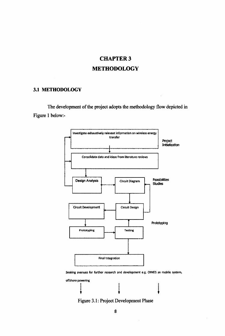
3.1 METHODOLOGY
The development of the project adopts the methodology flow depicted in
Figure 1 below:-
Investigate exhaustively relevant information on wireless energy ,.. transfer
I
• Consolidate data and ideas from literature reviews
1-t
1 Design Analysis Circuit Diagram Feasi
'-- ~ Studi
Circuit Development Circuit Design
t-
Project Initialization
bilitles es
! Proto typing
Prototyping Testing
Final Integration
Seeking avenues for further research and development e.g. OIMES as mobile system,
offshore powering
Figure 3.1: Project Development Phase
8

3.1.1 Project Initialization
3.1.1.1 Document Research
In achieving the objectives on the suitable concept of the project, there are
various types of research have been done. One of the researches being done is
document research. In finding and selecting the most suitable and feasible concept,
there are many documents that have been viewed, covering from articles, journals,
magazine and theses. From this research, the most feasible concept for the project
has been discovered. Apart from that, some of the theoretical and calculation
examples and guidelines were also gained from this research. This research also has
discovered improvement method that can be integrated to the project.
3.1.1.2 Internet Research
Another type of research that has been done in realizing the objectives of the
project is internet research. This type of research is used since it is fast and easy to
obtain information from all over the world. The purpose of internet research is the
same as the document research; to find the most feasible concept for the project and
improvement method that can be done. In addition to that, this type of research is
beneficial especially in finding the international standards for electromagnetic related
appliances which have been set by international bodies like Institute of Electrical and
Electronic Engineers (IEEE), American National Standards Institute (ANSI) and
Federal Communication Commission (FCC). These standards will be applied in the
project, parallel with the project objectives to design a safe working model. (Please
refer Appendix II for the standards)
3.1.2 Feasibility Studies
3.1.2.1 Design Analysis and Circuit Diagram
From the research done, the basic concept of the project has been acquired.
On top of that, I have discovered some methods that can be applied to improve the
9

perfonnance of the project. From the infonnation of these concepts and improvement
methods, the draft circuit of the project prototype has been designed. The design
process has considered all the requirements needed so that the circuit is assured to
meet the project objective. This draft circuit then will be simulated to check its
perfonnances. Any improvement design will be done in parallel with the simulation
process.
3.1.2.2 Simulation
Project initialization and feasibilities studies as in phase I have been
conducted using PSPICE full edition prior to the development of the prototype. This
is to provide a feature-rich and fully scalable solution that can later be translated to
the prototype. The simulation is done to check the perfonnance of the designed
circuit. In addition to that, the circuit design improvement process can be done at the
same time. From this simulation, the actual value for each component required can
be determined. The results of the simulation will be discussed further in Chapter 4:
Result and Discussion.
3.1.3 Prototyping
3.1.3.1 Circuit Development and Prototyping
From the designated circuit in the simulation, the project moves to the next
phase which is building the first prototype. This first prototype actually consists of
all the components needed in the final prototype. The only difference is that the
prototype is developed on the bread board instead of on the printed circuit board
(PCB). This is purposely done since the main purpose of this prototype is to check
the perfonnance of the design. In other words, this prototype will undergo trial-and
error phase, where maybe there will be some modification need to be done to the
prototype.
10

3.1.3.2 Testing
In testing phase, the performance of the prototype is observed carefully.
There are various tests that have been done in order to test the performance of the
voltage doubler circuit. Besides that, the testing phase also includes the RF energy
harvesting test. The purpose of the test is to measure the performance of prototype in
harvesting electromagnetic energy (RF energy) in the air.
3.1.4 Final Integration
After the entire tests have been done with the value and type of components
has been fixed, the prototype then was upgraded to PCB as the final stage of the
project.
3.2 PROJECT PROGRESS
The project has progress according to the plan. Although there are some
problems in the middle of the project progression, the problems have been solved
and the project is back on the track. Please refer Appendix III and Appendix IV for
Project Milestone and Project Gantt chart, respectively.
11

CHAPTER4
RESULTS AND DISCUSSION
4.1 DATA GATHERING AND ANALYSIS
The data and information regarding for the design of the circuit generally is
from the theoretical part, which involves some calculations. Other information in
designing the circuit is observed from the simulation and prototype tests results.
4.1.1 Calculation Part
4.1.1.1 Length of Antenna
f=91SMHz
T = llf = 1.0928 x w-9 s
T/4 = 0.2732 x w-9 s
L=cxT/4, c=3x 108 ms·1
= (3 x 10⁸ ms"1) x (0.2732 x 10"9 s)
= 0.08196 m "' 8.20 em
4.1.1.2 Resonator
LC = 25330.3/ f, f= 915 MHz
LC = 25330.3/ (915i
=27.6834
Considering L = l J.IH,
C = 27.6834/ L
= 27.6834/1
=27.6834pF
For the explanation of the calculation, please refer Appendix V
12

4.2 RESULT
4.2.1 Simulation
These results are the simulation results of the receiver circuit. The simulation
is divided into two parts; the performance part and the improvement part.
4.2.1.1 Performance Part
The aim of performance part simulation is to check whether the proposed
circuit can produce the desired output. It is also done to predict the output voltage as
the number of stages increases.
The results of the simulation are shown below. (A) DoUbler.da~ {acl;ive)
lOV ' ' . ' ' ' I I I I I I ;:;--:----; ; ; ; -;---- -----,-----,---- ,----- -----:--- -,-----,---- ---- :··::Iz·---~:::;~: :~:f~::::;:::: ·:::~;:::: :;:::::r: ::: :::~:;:::::;:::::f::::: :::::;:::::~::::r::: :::::_;:::z __ ::;::: ::
w +---+"--+' -+' -1--i'f----i'--+'-+--+' -:-· -i''-+-i-' -..;-· -+-' .!.:19c::6p;22~7m~ .. ::_:•·c::""fB--+,---J
:::::r~:± ---+--+---1----- ----+----1---+---- ---+---+----t·--- ----+---1----+---· ~----+-·-· ::::;:::::;:::::c:: :::::l::::r::r::: ::::r::r:::r::: :::::;:::::r:::;:::::
""~-+.~.~~.--+-~.~~.--~.--r-~.--+.--.~+-T.--~. ~.--+-~.~.--~.---1 I I 1 I < I I I < I I I I I I :·_:J:::::J:·::::I. ·_·_·_·_ ----:---- ·:--- --:----- -----:-----:-----:----- -----:-----:-----:---- ---· -:-----:-----:-----
. ---- ~-- ---~--- --1----- ---- ·f·-- --!---- -r----- --- --~--- --~ --- ·+-- -- ----- ~- ----1-----1-----... --!--·· +----+---- ---- i-----i-----t~---- -----! -----!-- -- ·t· --·- ... ·+ ····+····+· ....... ·+····i··· --~--- ..
w 1--+;--+-;--~;-4i-~;---+;--+;--t--;i--i;~~;--+-~;--~;--.~: -4--~;---+;--~;~ . ----~ -----:.-----:.---- -----~-- "" -~- ----{·-· .••.•. -~- ...• ; •. ·--~----" . ----:. ··-·-i- .. ---!--- "" •••• " ~- ----{· --- .; •••• -
: : : : : : : : : : : : : : :
~~~~~~~~~~~~~:~~~;~~:~ :~::r~ ~~~r~~ ~~~~:~~~ ~:~:~r:~~ ~~r:~ ~~f~~~~ ~ ~ ~~~~~ ~~~~:~~~ ~~~~~~~~ ~:~:~~:~:~~r~~ ~ ~~~::~~ ~ +--t:--~: ~:--+-~: ~:--~:--r-~:--~:--~:~r-~:--~:~:r-+--+:~:r-~:~
.. ---~ ............ ---~. . .•. """ ·-:··· ··-:·· ---~---- .•.... :---- ·:-----~ ----- -----~-" ---~-----:----- .•.•. -:----- 1·· ···1· ... .
---- -r-----r~- ---r---- --- --+- ---+--- -1·- --- ---· -!- --- -~ --· --r----- ---·+ --- -+ -- --+---- -----1------1- ··- -1-----· ----r-----r-----r---- ····1·· ···1···· t· --- --·-·t··-· ·t··· --r----- · ----r --- --r --- --r--·· --··· 1· ····1·····i··---
OV Os ..... """ too~
a V(C\1:2.)
Figure 4.1: Output of Single Voltage Doubler Circuit
13

20V
1SV
lOV
sv
eov
<OV
40V
20V
,,
(AJ Doubler.dllt {active)
' ' ' ' . ' . ' ' . ' ' _____ , ____ _. -- ' ' ' ' -- ' ---- ----- --- ----- ------ - ·.:~---·-----·----·--
-~t::::r:::t::::_ ·::::t:t::t::: ::::t:J:::t::: ::::t::~~;~;b~ :~;~:t::L:r::: 1 {5~7 .28tu,12 064) ; 1 ; l ; ; l 1 1 i l l
' ' ' ---+---+···+-------··-----.. ----·'"·---' ' ' ' ' ' ---·r-- ·-·r-----r--------· r-----r· --- ·r ----
' ' ' --·--r --· --r---- ·r- --· ' ' ' ' ' '
~~:~~~:~:~:~:~:::~:::: -- ---r- --- -r-----r----
'"""' D V{Cl0:2)
' . ' . ' ' . . . ' ' ' ---+---+-·-+---- -----1--- -+---+ ---- --- -+----+ ---+- --- --- --i----- i--- -- i-- -------1---··i···-·i·· --- -----t-----t---- -r----- --- --r -----r -- --+---- ---· -1----+-- --1---------1---- ·1·----1----- -----t -----r-- ---r----- -----r---· ·r---- -r ---- -----i····--i··---1-- -------r --· ·r-· ··1·· --- -----i---- --r-- ---;·--·- ·-- ··r ----·;----;- --- --- ·-;- ----;- -- ··r·-- ------.:-- ---.:-----~--- -- -- .. -~- ----~ ... -- ~----- -... -~ -----:.-----:----- -----.:-----1--.- ·1-----
: : : : : : : : : : : :
::::~::: :~ ~:::::~~:::: :~::~~:::::r:::~:~ ::::~ :::::~:::::~~::::~:::: :::::~::::: ~:::: :~: :::: I I I 0 ' I ' I o I I I
----.:-----.:-- ... ~----- -----{-----~-- ---~ --·-- .. ---:.---- .;. ... -..;.. ....... --.:----- i -- ---i-· ---: ! : : : : : : : : : :
""" .... , ... lOOme
Ti
Figure 4.2: Output of 2-stages Voltage Doubler Circuit
(Al 7Dc-1Jbler.dac {active)
' I I I I 0 < I I 0 o I I t I o o I 0 I -- .............. --- ..... . . --·-- ................. - ----·- ................... -- .......................... ··--- -·-- ........... --. ' ' . . ' ' . -- --r-- -+-- -t--- -r ---
: : : : : : : ('25. 63m;66.l45) : : : : : :
---1~---j---+---1- --· ---- t_---+-· ·1·-- ~t---- ---+7'( --- i-·-+--- ----1----}---+---{----
----vy---r--T--- ·--r--T---:--·r· ----r--T-·rr-- --·r--·r--·rr· ----r--r----:---r--I I I 0 o I I I o I t I ,I o I 0 o o t I -- r--·r---·1·--T-- ---r---r··-r---r-- ----r··-T···r--·r··- --·r··-r--·r--T--~ ·---r---r--~r---r--
- M:. ---.:- ---~- ---~·- ...... -i~---~ .... ;. ... .:---- ---- V-- --:.-- • .,: ••• .:~---- ----:- ---i---- ; .... ;. ... --- -~---- ~----'-:. ----:-- .. i (7.~2tlit,42i031 i : : i i l : : l i : : l ; i i
- 0 -~ ----:----:·.;..!'·:--- 00 ---:•MO ·: ----:-··:··OM -- ••: .. 0-:---:---- t ---- .. -:---:----t· --:--- ----·:-- ._ :----:-.. :----r-r : : : : : : : : : : : : : : : : : :
I 0 I < < < I I < I 0 I I I 0 I o o I o
:::;:::;::::;::::;::: :::r::;::::;:: :;::: : ::::;::::;:::;:: ::; :::: ::r:;::: r: :;: :: ::::;::::;: :::;:: :r:: --+- --i----!-- --t--0. --- ~"·-+--+ --i-·--0 '"' +--+-M·i·---t---0 --~+---1----t-- -+--- ----'i-- --~- --+--+---
' I < I I 0 < I 0 I o ' I I I o I I o I I 0 I 1 I f < I ' < o o I I ' < I I I I
' : : : i : : :, : : ; ,: ._: : : : : : ' ' ----r-- ·t···r---·t--·· ---1""--!--- ·r···1· --- ----r----r---1----t---- -··t -- ·1--- ·t··--r--- --- ·1·-- -r-- --r·-·t ---• I ,I I I < 0 I I < I I < I I I I I, I 0
----~---~----:· ---~-- ·- -- -~----:--- -~--- ~- --- ---- ~-- --~-- -~---- ~---- ----:- .. -~- --- :---·:---- . -- -~- ... ~----:- --·-:--·-: : : : : : : : : : : : : : : : : : : :
----r---1··--r----r··-- ---1·---r----r---;---- ----r----r---;--·-t··-· ···t···;-·-·t··-~r--· ----1·---r-----;---1·---200ms """"' sooma
a V!Cl4:2)
Figure 4.3: Output of 7-stages Voltage Doubler Circuit
14

4.2.1.2 Improvement Part
For improvement part simulation, there are some tests done to check the
performance and to improve the output of the circuit. The tested circuit is shown
below:-
"' ~ ·= = ~
•• .•. C I . ~~tCm
011<035 Dt~ ~ 015
" "' · '"~ , ·is'~ "h~J t'·=.-~ '" , .• ,. ,, .. '" ,, w ~ "' ¥ = 00
t--+--<f--'----"---Ji---J__J_:DI:N~C~ J_ ,_ ~f-· --'---'---0<'-jlY!'; Cll, :Jtlll.."ll c:Mf--I--J-O_"~~=~__J--;--iL-lQI• iC.· ,QI, ,.. jQI, 1
oi~.,., D1=
~ '" .•. .•.
Figure 4.4: 7-stage Voltage Doubler Circuit
The conditions of the circuit are as follow:-
:SV
:10kHz
"' _.,
Input Voltage
Frequency
Stage Capacitor : C3, C4, CIS, Cl6, Cl7, CIS, C19, C20, C21, C22, C23,
C24, C27, C28
Output Capacitor : C14
There were three tests being conducted:-
• Test 1: To compare the output performance between circuit that use same
value of capacitor in each stage and the one with different value of
capacitor in each stage
• Test 2: To find the best stage capacitor value
• Test 3: To determine the optimum value of output capacitor
Some of the results are shown in the next pages. For other simulation results,
please refer Appendix VI.
15

eov
<OV
40V
20V
ov
aov
60V
40V
20V
Test 1: Stage capacitor (same value versus different value)
Os
(AI 7Double~.dat {active)
I o o I o o o I I I I 1 o I I I ' o I 0 -- ............ -·--- ...... ---~----·-- ............. --- ................. -· ---- --- ----·----·----.. --- --·-· ----· .............. . . ' ' . . ' ' ' ' . ' . . ' ' ' ' ' . . -- -~r---1-- --!---+---- ----1- ---r----r----1~--- ----r_-.~~-r~:~l~Y?-7 ~~ --j----1---- r-- --r --- ----1---- r·_~--~r- ---~--------:·--:----:-~ --- --
1: : : : : : : : : : : : : : : : : : : : -··r--·r--T···r-- ----r-··r···r-··r-· ----r-··T·--r-··r-·-- ---T·-·r···r··-r··- ···-r···r-···r···r------:----~- ···t·· ··r··-· · ··1··· -~ ----:----~---- ----~ ·· ··:-··· ~----:-·-· ·· ·-:-···1···· :·· ··:- ·· · · · ···1·· -- ~--·-:-· ·· -:----
---r--+ ---t-- --t-- -~ ---1---- r----r- -- -~~- -- -- --r----- -r---1---- t-- -- --- -~----1---- t----r --- ----1-- --r ----r---1----I o o < 0 I I I I o t 0 o t o I t t o o I I t I o 0 o t ---+ .. --i.--· ·!, --- .,.,: --- --- ~- ---i~---~---~---. --- -~--- -~- --~-- --t---- --- -l----i --- -i -- --~- ...... { ... -~- .. -~---~- ---I I 0 I : i : : : : : : : : : : : : : : ----r-··r ··r· ··;-- -----T ---r --r --;---- -- ··r·· ··r···r -- r- -- --·r···r·· i ----;··- -· --t ··r ····r -- ·r··-
----r---1·---;-- --r---· ···;---- t··-·r·--;---- --- -;----;---;-- ··t ---- --- ;···1·---~ ----~--- ----1····r · ---r---;----lOOms 20.0IM 300ms _SO Oms
a V(Cl4:2) Timo
Figure 4.5: Different value of stage capacitor
0 t t I -- .............. ----~---. ' ' ' I < I t . . ' . -- --r-- ·1··· "t" ---r--------vr---i----i---
-- ~[--+-+-+--- -~----.----~---·····
; P-~211it,_42io:s1 . ··:-•---:----1-~-r-··-
(A) 1Doubler.dat {aetive)
t I I I I I 0 o I t t o I I I 0
::: r:: err:: ::::r::::;: ::;:::~1~~:-: ~;~~~~t!:)::::;::: ::::;::::r: :::;:::;:::: --- .. --- .............. -- -- --·----- ......... ·---- ............ --- .. ....... .. --- -·-- ................. . . ' ' . . ' ' ' ' ' ' ' . . ' ' . ' ' ' ' ' ' ' ' ' ' ' ' ' . . ' ' . ' . ' ' . ' ' ' ' ' ' ' ' . ' ' . ' ' ' ' ' ' ' ' ' ' ' .
' ' ' ' ' ' ' ' ' . ' ' ' I I I 0 I o t I t t I I 0
' . . ' ' ' ' ' ' ' ' . ' ' ' ' --·r- --I ----r···r·--- --- -r- --r ··r··; ---- --·r --- r- -- r- ·-r --- ----r --T ··-r·· ·r ------1·· ··t··-~r--·1·--- ----;- ---r- --;--·-·t ---- ---t ---i- --- t··--r --- --- -;----r"- --;-- -;---· ···:··· ·: --- -;- ... :· .... ···:-·- ·;----:·-- ·: ....... :· ··:-· ·-: ---~;- ... ----:----:-- -~;---- :- .. .
: : : : : : : : : : : : : : : : I I t t 0 I t t t t I
' ' ' ' ' ' ' ' ' ' ' t t t I I I I I t t t I I I I ' t t t I
::r:rr:r: ·:::;::::;::::r:::r: :::r::;:::r::;:::: :::r:r:::;::::;::: ::::;::::r:::r:r:: -·--~----:~----f .. --~·--- ---1--- ·t··· -:-----:---- .... ~-- ··l-·· --:- ---+---- . ---:--- ·i··· ·t. ···l-· .. -- --i .. --1- •• --:-----:----
: : : : : : 1 : l : i i i i i i ! : l : ' ' ' ' ' ' ' ' . ' ' ' ' ' ' ' ' ' ' ' ' ' ' ' ' ' ' ' . ' ' ' ' ' ' ' ' ' . '
:: ::~:: l::;::::~::: :::;::::1: :::~: ::;:::: ::::~::::~:: :;::::;:::: ::::j::::r: :;::::t::: ::::;::: :[::::~: ::;:::: ----r, -- ·i,···-t, ----r, --- ---~---- ~----~- --~-- -- ·· --~----:- ·· -~---- }-- -- -· -~-- --~----{.- ---:---- ----:{-- --~----:-- --~--- ~
1 t : i : i ! -t ! t i i i i i : crv ~~--~._~-+--~~~~--+-~~~~~-r~--~~~-+~._~~~~ Os lOam. 200ms 300Jrul 400:m:J SO Oms
a V(C14:2) Iime
Figure 4.6: Same value of stage capacitor
16

eov
•ov
40V
20V
lOOV
aov
60V
40V
Test 2: Stage capacitor (different value)
,,
{A) 7Doubler.dat {actiye)
I I I I I I I I I I I I 1 I t I o I 1 ......................... ---·----·----.. ·-- .. ·-·· .......................... -------·----·--·•>-··· ---- _________ ,__, ...... . : : : : : : : : : : : (~25. 63m~66. 7451 ! ! : : :
----r--+--+ ---r--- ---i~---F- --1----+ --- ----~----+-- +---t--~- ---+?:---- -t.----~--- ---- ---+- -- +-- -+---···'n-·T··r· ···r·r·rT·· ····r···rT·T··· ··-rT··:···r· ---· ···rT·T--, : : : : : : : : : : : : : : : : : : --1~ ---+· --:----~-- .. -- -~----~:---+-- ~---- .. --~ -- -+--- ~----!-- -- -- -+ ... ~----:-- --~ .. -. --- ---- ~----~ --- ~----
' I I I I I I I I I I I I I 1 I I I I 0 I I I I 0 I I 0 0 0 I I I 1 I 0 I 0
·~---~---~-~--- -~---- ---~- .•• ; •. -~~-- --l~--. ----~-" ---~- ---l~-- .-; •.•• ----:----~- ••• ; •.• -:.--- --·- ·---~- ---:.-- --l· ·-· i J_7.~2u.it,42la:n 1 L : L i· .] i -.1 .: i :_ i !-. i i
-· --~- --·~---·'-~-}-~--- --- ·1··-·t----~---·v- -- ·· --~-----:----~-----+---- ----:---- ~---- t ----:- ··- -- -· -- --~----:-- ---:----, I I I < I I I I I I I I I I I I I I I I < I I 0 I •I 1 I 1 I 1 I 1 I 0 I I I I I I I I 1 I 1 I 1 I 1
I I I I < I I I I < I o I I I I I I I 0 I I I I 1 I
I I < I I I 0 I o I o o I I I 0 I I 1 · --r·--;- ---r -- ·r· --- -··t ·-r-· --r·--;---- ----r··--r- --1·-··t·-- ----~--- -;--- ·t··-r·-- ---- --- -;- --·r ---;- ---·-+· --~----~ -- --~ .. .. --+ --- :·--+---~·--- .. --~--- +---~----:-- -- .. -+--- ~----: ----~ --- ---- ---+----:- --~---
---~-- -~----i----~---·- ·- --~~- --i----~--- ~---- . ---~-.... ; ... -~--- -i---- ---~----~--- -i~---~--- ---- ----~-----~---~----1 I I I I I I 0 I I I 0 0 I I I I I I I I I I I I I I I I I I 0 I I I I I I I 0 I 0 I I I I I I I I 0 I I I I I I
0 I I I I 1 0 I 0 1 0 1 j 0
·--~-- -~-- --t----~---· --- i----i-- --~- --~"-·- ... -~·--- ~~- --~-- .. f ---- ----~---~----·--· -~--- ---- ----~-- ..• : •.. -~----: : : : : : : : : : : : : : : : : : : I I I I I I I <, 1 I 1 I I 0 I 1 1 1 >
··•'-'- """"'" •••,h "••'-• ••• ••••••·•••••••'-··• "'" ••• ••••L'••••'-••· •••••-••·•• ...... ··•"• ••• •••••'- •• 0 ·•• • •• •• L•·••'-••• .. •••• I I 0 0 I I I I I 0 I 0 I 1 1 I 1 0 1
: : : : : : : : : : : : : : : : : : : ----;- ·-;--- ·1··- ·t --- ---;---- r-- ·-r·--r·-- ----;- ---r- --;----r---- ···t··-i --··t·· -r--- ---- ----;-- --r---1·--·
200JM """"' 400:ma SOOl!IS a V(C14.:2j
Figure 4.7: Capacitor value= 10 nF
(A) 7Doubler.d.at (active)
' ' ' I 0 0 I 0 0 1 1 I I I I I I I 0 > I I I 1 I
I I I I I I I I I I I 0 0 I I I 0 I I 0 I I I I ....................... ---·---·---·-·- ... -- ----------------- ---~--- ... ·------·-- ---·---······-···-· .................. ~--' I I I I I I I ' 0 I I I I I I I I I I I j I I I I I I I 0 _I 0 -- ·r·--r-·i···i··- --·r-·--r~-~r--·-r -- I 0 I I I I I I I I I I 0 I 0 I
-~r-·1···1~· -: ~-- ·· ·r---r;~t·-~r-- ·-··t·· ·t·~-r---r-·w ---r-·t ·-1~--·1··· ··r-·r-·r··r·· ···r-·r··r·--r·· ···r-·1· ·-;·-~t--· -- ·t ··-r··;-··r-· -··r--r··r-·r--- --·r··r ··1···r··
tttf !!f! !+1 1 iLl! !f!T'~ I 0 I I I I I I I I 0 I I I 0 ,I I I I I I I I I -~~~~~+~~~~~~r~~ :~:r~:~~~~r:~~~~ :~;~:~~~~r~~~:~~ ~~~r~~r~;:~t~: ~~ ~~~~:r:~~~~~~~:~ :~~~~:~~~~~~~:r~~
~ ··r···r-·1· ··r- --· t···r-~;- -~r-- ···t-·1·--;-··t· -- --·r·--r-- -;- · --;--- ---;-- -;- ··t···r·-- -- -r---~- ··1···;··-I o o I ' I ' I I 0 I I I I > I I I I I I 0 I I I I I I I 0 I I I I I I I I I I I 0 I I I 0
··t··1· --1"" ·1· -- -- -r---r- ·_t --·r-- ---1-- t··t··-r--- -- -r-·t-·1·-·_i·--
:TFFF ::rFFF :::;:::;::r:;::: :::;::FFF ---r---r-·i·--1-· · --- t· ··t·· -r-·-r--::FFFF :::;:::;:::;:::;::
I 0 0 I I I 0 I I I I 0 I I I I I I I t I I I I I 0 I I I" I I ,I I I I I t_ I I ,I I I I I I I I, I
~~~~~~+~~~~~~r~~ ~~~~-~~~r~:~:~~~~~- ~~+~~~~~~~~~~f~~: ~~:r~~;-~~+:~r~ ~::-r~:r~:-r:~~~:~ :~:~:~+~~;~:~r~: · --~---:- ··i·· ·i··· ---r---t---~---~-- ···t -- i··-i· ··t··- --- t---~---~--t-- -- ·i··-1··-t·--r--- ·--~·-t··i··· i···
av ~~· -L'~·~·~~~·~·~·~·~~~·~·~·--·~t-~·~·~·--~·-t~·~·~~· -L'-t~·--·~~·~·~·_, Oe O.Ss l .• Oe 2.08 2.5e 3.0::1
o V{C14t2)
Figure 4.8: Capacitor value= 100 nF
17

eov
61lV
40V
2W
Test 3: Output capacitor
(A) 7Doubler.d4~ {active)
' ' o I I, o I ' I o o o o ··· ·:-····r· ·-- r···- ··--·:·· ·- ·r-····:·---- -- ··-:····-:····-:···- --·-·r·· ··r···-r----' ' ' ........................
' ' ' ' ' '
-----r-- --+--- --r-- -- ----1·--- -·-;-----f····. --- --~-- ---f---- ~t- ---- --- --~---- +- ---+---- -----+----1----- ~-- ---I o < I o I I
I! .......... ---- -................ -- --· .. --· ---- .•... --· -----·---- ....................... --- ---- ......... --- ·-· -----' I o > 0 > I I I I t I I I < o I I I o o I I o I 0 o I I o o o I I o I I o o o o o o I I o I 0 o o o I o o I o
' ' ' ' ' .. -·--·-·'"··-- ...... . ' ' ' ' ' '
-·-·t' 0;9i4lm;t4-.-325. ' '
···-t : : ' ' '
:::r:::;::::r:: ----·r- ----r-----r----
I o I I o I I o ' ' . . . . ' ' o o o o o o o o ' I o t ---- r··-;-----;----- ---··r·- --r- --T ---- ---··r····r-··r --- -----y-- ··1·----r- ---
-- ··1·----1-- ---1----- ----- ;---- ·t··---; ----- -- ---r---- -;--- --r---- -----1-· --·J··-· -;-------··r··-·r··--r···- ---··t·· ·-· r··-- ·r· ·· -- -- ··-r·· -- -r· --- r··- · ·· · ·r·---1·--·-r·---
' ' ' ' ' ' o ' o o I o o o o I o I
::::r:::r::r::: :::::r::::;:::::r::::: :::::;::::r::r::: :::::r:::r:::;::::: -- --1·----·[·- -- -;·-- -- ---- -t~--- ·1 -----r----- ----~r- -- --r -- ·-t--·- ------[----~-, ___ --1-----
'
-_-_-_-_-_r~:· -_-_-_-_-.r~:· -_-_-_-_-_1~:~ -_-_-_-_ ---- Ji··-- ··1·--·-l··--- ---··f·· ---t-- -- ~r- ---- --- --r-- -- -r---- ·j·---- -----1·----t--·--i·· ----- ··r· ···-r··· ·1··· -- ----- i---- ·r·--- r·---- -·-·-r-···-r··- ·-r··-- -----r · ···1···· ·1····-
--·-·t··-- -r--- --r---- --··t --- -;-----;-- --- ----- ~ ----- t· --··t··--- --- --; ----t ----t ---- · -- --;-----1·----~ -----ov -r--~~--~--+-~~~--~--r-~--~~~-1--~--~~---r--~--~_.--~
eov
60V
40V
20V
llV
Os 0.2e 0. 4e o-.6:9 0.83 l.Oe _a V(Cl4:2)
o.
Figure 4.9: Output capacitor= 1 nF
(A) 7DPUbler.dar- {acr-ive}
' o I ' o ' 0 0 0 I o I o I o I · ·-· ·r · ··-·r··-· -r··--- ·· ··r····;··-··r· ··· ··-· ·r··-· ·; ··· ··r·· ·· · ·····r · -- ··r ·---T-- ·- ----·r····;· ·· ··r··· ·
· -·-·t · -- --r-- ---r---- -- ··1·· ···1··-- ·1----- --·-·t··- ··1 ----;r----- -----:-----:-----:--- -· ------~- ----:---- -:· -- ·-""";;<":, -----·-- -- -----·---- ------- ·----- ----- ·-- ---·-----· ----- -- ---·-- -- -·- -------- --- --·-·--- ·-----·-----1: i i 1 i i i 1 i ! i ! i f
' . ' ' . ' ' ' . I I o I o o o I I
' ' ' ' . . ' ' ' . ' ' . ' . . "--~---- ...... ........ . ................. ·----" -----·----- ·- ----~--- -- -- ...... -............ ---- . -- ......... ·----- ·-----: i i i : ; l i ; : l i ) ! ;
---·r-----~=12~m;~ ~et· ···1· --· ·1"···· · --··t -- ··t··· ·-r----- -----r ·----r ---·t··-· -----1· ----_;---··t··· · ·--~t-----... ---· -·-·r····r··-·r-·-- --·-·r···-r··-·r·---- ---··r···-;·-··r··- ·····r···;-·-··r··--
' . ' ' . . ' . I 0 0 0 I 0 I ' 0 I I •
::::r::r::r::: ::::r::r::r::: ::::r::r:r:: :::::;:::::r:r::: ----r----y- -- ·1·---- -- ---1~ --- ·r--- -- r----- -----r- ----; --··t·· -- -----r ····1· -- ··1··· --
. ' ' . . . ' ' . • • ' • • • • ' l
' ' ' ' ' . . ' . . ' . . ' ' "----:-----~·--- --~---- -----:---- -:--·-·i·· --- . ----:~-- ··t···--:----. ---·-:--- ···:-- ---:-· ... -.. --:-----·: ----- f·····
-----r--- -+----+---- --- -+-- --+- --- !"---- -- ---r.~--- -r----~r ----- ----+- ---+--- -+---- -----1-----·1-----1- -------- ·t···--r- --- ·r--·- ·-·--i·--- ·t··--;~- --· -----!c.·--;·- --··r----- --- ··;---- ·r· ···"t· --- ---- ·1·----i ------1·····
0.2!1' o.4e 0.6e o.el!l l.Oe o V\Cl4:2J
I
Figure 4.10: Output capacitor= 10 nF
18

Test 1: Stage capacitor (same value versus different value)
Table 4.1: Result of Test 1 (lmprovement Part)
Stage capacitor value Output Voltage (V) Rise Time (s)
Same value (10 nF) for 66.75 7.62m
each stage
Different value (0.1 nF to 65.33 14.52m
10 nF) for each stage
Test 2: Stage capacitor (different value)
Table 4.2: Result of Test 2 (Improvement Part)
Stage capacitor value Output Voltage (V) Rise Time (s)
1nF 63.50 19.04m
2.2nF 65.40 12.22m
4.7nF 66.32 9.41m
10nF 66.75 7.62m
22nF 67.05 -47nF 67.16 -100nF 67.19 -
Test 3: Output capacitor
Table 4.3: Result of Test 3 (Improvement Part)
Output Capacitor Value Rise Time (s)
lnF 6.72m
lOnF 8.12m
19

4.2.2 Prototype
These results are the results of prototype testing phase. The testing phase is
divided into two parts; the receiver perfonnance test and energy harvesting test.
4.2.2.1 Reeeiver Performance Test
In this testing phase, the performance of the prototype is observed carefully.
The first test was to test the perfonnance of the voltage doubler circuit. In doing this,
the input of the receiver is connected to the ac power supply to get the AC voltage.
The result of the test is shown below:-
Table 4.4: Voltage doubler performance
Number of Stage Input Voltage (V) Output Voltage (V)
1 3.0 7.1
2 3.0 13.2
3 3.0 13.1
4 3.0 12.6
5 3.0 12.4
Based on the result above, it could be observed that the voltage doubler did
not perform as it should be. The maximum number of stages that it could support is
only two. Re-examining the components, have shown that the problems were sourced
from the capacitor where its voltage rating is about 12 V.
Knowing the source of the problem, all the capacitors were changed to the
electrolytic-type capacitor with the value of 1 micro-Farad with voltage rating of
50V.
20

Figure 4.11: Prototype receiver with new electrolytic-type capacitor
New Capacitor
Value : 1 J.lF
Voltage Rating : 50 V
The performance test of voltage doubler circuit was done again. The results
are shown below:-
Table 4.5: Voltage doubler performance with new capacitor
Number of Stage Input Voltage (V) Output Voltage (V)
1 3.0 9.5
2 3.0 18.6
3 3.0 25.3
4 3.0 32.7
5 3.0 36.4
Based on the result, the new design looked promising. The supported stage is
up to five stages. Although the increment of the output voltage was decreasing, it is
acceptable since the decrement have been predicted theoretically.
21

Continuing from the current design, the number of stages was increased to
eight stages to test whether the pattern of the output voltage continued. The result is
shown below:-
Table 4.6: Voltage doubler performance for 6, 7 and 8 stages
Number of Stage Input Voltage (V) Output Voltage (V)
6 3.0 36.9
7 3.0 35.7
8 3.0 32.3
Based on the result, it showed that the highest output voltage could be
produced from 6-stages voltage doubler instead of 7 -stages and 8-stages voltage
doubler. Starting from the 7 -stages design, the output voltage was decreasing. Re
examining the circuit design and the theory of voltage doubler, the source of the
problems was indentified. This will be discussed later in discussion part.
To solve this problem, there are some steps suggested needs to be taken:
• Change the germanium diode to Schottky diode, 1N5817/ IN5818/
1N5819. This is suggested to amplify the input into a better output since
Schottcky diode is a rectifier diode. By amplifying the input into higher
output, it is predicted that the voltage drop would be lowered and the
number of stages could be increased.
• Solder the components onto circuit board instead of plugging the
components into the breadboard. This is suggested to minimize the effect
of internal resistance in the breadboard thus increasing the output value.
Based on the previous test result, it was suggested that the diodes were
replaced with Schottky diode, due to that Schottky diode is a power diode (rectifier
diode). By changing the germanium diode to Schottky diode, IN5819, it is expected
that a better output could be produced since the voltage drop could be lowered and
the number of stages could be increased. The basic specifications of Schottky diode
are as follow:-
22

Model No
Voltage Rating
Current Rating
: 1N5819
:40V
: 1 A
Figure 4.12: Receiver with Schottky Diode (7-Stages Voltage Doubler)
Like the previous circuit, this circuit also tested with 3.5 V, AC input voltage
to check its performance as voltage doubler. (Capacitor value is maintained, which is
1 J..lF) The result of the test is shown below:
Table 4.7: Voltage doubler performance (with Schottky diode)
Number of Stage Input Voltage (V) Output Voltage (V)
1 3.5 10.5
2 3.5 18.5
3 3.5 27.7
4 3.5 34.6
5 3.5 38.9
23

Based on the results above, it could be observed that the voltage doubler did
not perform as expected. Same as the previous circuit, as the number of stages
increase, the voltage increment is decreased due to voltage drop. From this, it was
decided to increase the value of the capacitor to a higher value.
Firstly, the capacitors of 1 1-1F were replaced with capacitors with the value of
33 j.IF, 50 V. The test was redone and the result showed a promising result as
depicted in table 2 below:
Table 4.8: Voltage doubler performance with new capacitor value (33 !!F)
Number of Stage Input Voltage (V) Output Voltage (V)
1 3.5 10.5
2 3.5 21.3
3 3.5 32.1
4 3.5 42.6
5 3.5 53.4
6 3.5 64.1
7 3.5 74.3
Based on the result in table 2, it could be observed that the voltage doubler
circuit work better that expected. The increment in voltage doubler stages did not
affect the performance of the circuit. By this, it was proven that Schottky diode is
suitable for this type of application (rectify and amplify the input voltage). The
voltage drop also being lowered thus stage increment could be done without any
problem.
In order of testing the performance of the new circuit, the capacitor value was
increased again to 330 j.IF. After replacing all the capacitors, the test was redone. The
result is shown below:
24

Table 4.9: Voltage doubler performance with new capacitor value (330 !!F)
Number of Stage Input Voltage (V) Output Voltage (V)
1 3.5 10.7
2 3.5 21.9
3 3.5 33.0
4 3.5 43.1
5 3.5 54.1
6 3.5 64.7
7 3.5 74.9
Based on the result above, it could be observed that the performance was
about the same as the circuit with 33 1-1F capacitors. The voltage increment was not
very significant. This is maybe due to that the output voltage has reached its
maximum value for each stage.
From the result of all tests, it was suggested that the receiver prototype would
used the following components:
• Schottky Diode (1N5819) - the performance of the diode have been
proven in amplifying and rectifying the voltage
• 33!!F capacitor- The 33!!F capacitor is preferred compared to the 330!!F
since the performance is about the same. Besides, the size of the capacitor
is smaller and this is crucial in minimizing the overall circuit size.
25

4.2.2.2 Transmitter
Basically for the transmitter part, there will be two phase. The first phase is to
purchase the transmitter in the market and used it to check the performance of overall
prototype. The second phase of transmitter part concern on designing the transmitter
based on specification needed.
For the first phase, a transmitter had been purchased where it could transmit a
300 MHz signal. Initially, a 915 MHz transmitter was preferred. However, due to
unavailability of the transmitter in local market, another transmitter was purchased.
This transmitter would function as performance checker of overall prototype as well
as become the base design of the designed transmitter (phase two).
Figure 4.13: 300 MHz Transmitter
The transmitter had been tested and it worked as it should be. However, there
was a drawback of using this transmitter. As observed from the figure 2, there was no
external antenna, since the antenna was printed at the back of the board (Printed
Antenna). The disadvantage of this type of antenna was that, it is a directional
antenna. It means that the receiver antenna should be in line with the transmitter
antenna to receive its signal. However, this was not a big issue since the transmitter
was used only as a performance checker.
26

It is suggested that an external antenna can be attached to the transmitter so
that the signal can be transmitted in various direction (Omni-directional antenna).
4.2.2.3 Energy Harvesting Test
Another test conducted was energy harvesting test. The test was done to test
the performance of the prototype in harvesting electromagnetic energy in the air. In
this test, the antenna was connected to the input of the prototype, replacing the AC
power supply. The output of the receiver was connected to the voltmeter to measure
the output voltage that could be produced.
There were two tests being carried out. The first test was done using the first
built receiver circuit which was using germaium diodes. The second test was done
using the redesigned receiver circuit which was using Schottky diodes. For each test,
there were two type of tests being done; harvesting ambient electromagnetic energy
and harvesting energy from transmitter.
Figure 4.14: Receiver Prototype
27

Table 4.10: First Part (Energy Harvesting Test) Result
Source Output Voltage (V)
Ambient electromagnetic energy 0.002
Ambient electromagnetic energy 0.120
(properly grounded)
RF signal from transmitter 0.200
RF signal from transmitter 2.100
(properly grounded)
From the first test (using receiver with germanium diodes), it was concluded
that the antenna need to be grounded properly, as well as the circuit. This is because
without proper grounding, the gain of the antenna become lower, thus reducing the
amount of energy harvested. This is proven in the test where a proper grounding
antenna would produce a far better output compare to antenna without grounding. In
this test, human body and metal material equipment/ parts become the source of
grounding.
In order of improving the energy harvesting process, two steps are
suggested:-
• A proper grounding should be done to the antenna to improve its
performance. The method of proper grounding should be researched to
minimize its size so that the prototype would be optimum in size and
performance.
• Another step that could be taken is to use an antenna that does not need
grounding at all to operate optimally. An example for this type of antenna
is dipole antenna. However, there is a drawback to this step where the
length of the antenna would be longer than the antenna with grounding
method.
28

Figure 4.15: The antenna (Monopole antenna)
The suggestion from the first part was integrated in the second part of the test.
In the second test (using receiver with Schottky diodes) of energy harvesting test, for
the first phase, we connected the antenna to the new receiver circuit (the circuit with
schottky diode) and observed its performance in harvesting ambient electromagnetic
energy. The result showed that there was no voltage gained (output voltage = 0 V). It
meant that the circuit failed to harvest any surrounding ambient energy. Next, the
circuit was tested with the signal from the transmitter. The result was still the same;
there was no output observed. The only explanation to this phenomenon could be due
to the input voltage where the voltage gained from the energy harvesting activity
maybe too low for the diode to operate.
From this unexpected result, the receiver circuit was redesigned and the
germanium diode was placed back instead of the schottky diode. The redesigned
circuit was connected to the antenna and its performance of the first phase was
observed. From the voltmeter, it could be observed that this circuit successfully
harvest ambient electromagnetic energy. At 4-stages voltage doubler, the receiver
managed to produce an output voltage of 0.12V. From this result, we tested the
receiver in harvesting signal from the transmitter.
29

The result of the test is shown below:
Table 4.11: Distance versus Output Voltage (Energy Harvesting Test)
Distance (em) Output Voltage (V)
4 2.4
6 1.8
8 1.2
From the result, it showed that the receiver hasd successfully fulfil its
requirement in harvesting energy for wireless electric application by producing DC
voltage at the output. However, the output gained kept changing due to various factor
such as surrounding air, directionality of transmitter antenna and receiver antenna
gam.
4.2.2.4 Final Prototype and Application
Using the result from the previous test (energy harvesting test), the fmal
prototype of the receiver was built. This final prototype was tested again with energy
harvesting test (harvest energy from signal generated by the transmitter) to make sure
it operated as intended.
Figure 4.16: Final Prototype (Receiver and Transmitter) 30

The result for the test is shown below:
Table 4.12: Distance versus Output Voltage
(Energy Harvesting for Final Prototype)
Distance (em) Output Voltage (V)
1 5.39
4 3.04
6 2.12
From the result, it clearly showed that the energy of the signal generated by
the transmitter had been harvested, rectified and amplified by the receiver circuit to
produce DC voltage. In fact, the DC voltage produced was slightly higher than the
one obtained with the first prototype.
Continuing from the test, the prototype was tested for daily application. For
application part, the DC output of the receiver was connected to a battery charging
circuit. This simple battery charging circuit would charge two AA batteries. This
circuit was used since it required low DC voltage to operate which would
accomodate the output produced by the receiver circuit.
Figure 4.17: Simple Battery Charging Circuit
31

Figure 4.18: Overall Circuit (Charging circuit, Receiver and Transmitter)
Using as a voltage supply for the charging circuit, the battery charging rate
was measured. From the observatio~ the charging rate for the batteries was 0.5 m V
per hour. The charged batteries could be used for various application like lighting a
small bulb, used in walkman, camera and other low voltage appliances.
32

4.3 DISCUSSION
4.3.1 Simulation
4.3.1.1 Performance Part
The purpose of this simulation was to check whether the proposed circuit
could produce the desired output. For this simulation, the antenna was replaced by
AC source since the output of the antenna would be in AC form. The input was set to
5 V for easy reference and observation. From the results of the simulation for a
single voltage doubler circuit, it was observed that the proposed circuit had satisfied
the requirement as a voltage doubler circuit since the output was about the double of
the input. As the number of stages increased, the output value was also increased.
From the results, it was also observed that addition of stages would increase the
output value about 9 to 10 V. Analyzing from this simulation results, the general
equation for determining the output value is stated as follow (as long as the value of
the stage capacitor is the same):-
Vout "' 0.95 (N) (2 V in)
where Vout =output voltage
4.3.1.2 Improvement Part
N = number of stages
V in = input voltage
The purpose of this simulation was to determine the value of stage capacitor
and output capacitor that would be used in building the prototype. There were three
tests being conducted. The first test was to compare the output result (output voltage
and rise time) between putting different value of capacitor in each stage (e.g. Stage 1
capacitors= 10 nF, stage 2 capacitors= 4.7 nF, stage 3 capacitors= 2.2 nF and so
on) and putting the same value of capacitor for all stages (e.g. stage I capacitors =
stage 2 capacitors = stage 3 capacitors = .... = 10 nF). Based on the result, it could be
observed that circuit with the same value of capacitor for each stage had slightly
33

higher output voltage and faster rise time. This was due to the different charging time
between capacitors where the circuit with same capacitor value had the same
charging time for each stage while the circuit with different value of capacitor had
various charging time which some of them were slower than others.
Continuing from test 1 was test 2 where each sub-test would use different
value of capacitor while each stage had the same value. The purpose of this test was
to find the best value for stage capacitor that would give optimum result. Based on
the results, it could be seen that as the capacitor value was getting higher, the output
voltage became slightly higher (about 0.03V - O.lV increase) and the rise time
became shorter. From this, it could be concluded that the higher the capacitor value,
the better the result was.
For test 3, the output capacitor was tested with different values. Based on the
result above, the capacitor with lower value (1 nF) gave faster output response
compared to another value (10 nF). Like the first test, this was due to the charging
time of the capacitor where lower value capacitor had faster charging time compared
to the higher value capacitor.
Conclusion of the simulation circuit
• Stage capacitor
o Same value for each stages
o Higher value give slightly better output ( ouput voltage and rise time)
o Value that would be used = 100 nF
• Output capacitor
o Lower value give better output response in term of rise time
o Value that would be used = 1 nF
34

4.3.2 Prototype
4.3.2.1 Receiver Performance
In receiver perfonnance test, there were various test have been done. The first
test was done using 100 nF capacitor. From the result, it could be observed that the
receiver did not produce the expected result where the output voltage is around 12 to
13 V only instead of 67 V (from simulation). Checking the condition and the
components of the circuit, the source of the problem was due to the rating of the
capacitor where the voltage rating is 12 V. From this result, the capacitor was
changed to electrolytic-type capacitor (value of 1 microFarad and rated at 50 V)
For the second test, initially the circuit showed a promising result where the
output voltage produced was as the expected value. However, by increasing the
number of stages to 6, 7 and 8 stages, the output voltage become 'unstable' where the
highest output voltage was produced from 6-stages voltage doubler instead of 7-
stages and 8-stages voltage doubler. Starting from the 7-stages design, the output
voltage was decreasing. Re-examining the circuit design and the theory of voltage
doubler, the source of the problems was indentified. It was due to the voltage drop.
When there is output current, there is also an AC current through the capacitors,
resulting in a voltage drop and a lower input voltage for subsequent stages (6]. The
equation for voltage drop is shown below:-
when;J
..
ilU : voltage dmp I : output (:urrent f : lnpttt. frequent:v C : capacity of caps .. n : # ofstages
Due to the voltage drop problem, the germanium diode used in the circuit was
changed to Schottky diodes, a type of power diode. With capacitor of previous value
(1 J.lF, 50 V), the receiver circuit was retested. From the result, it could be observed
that the output voltage produced was not very high as expected. Considering the
condition of the circuit, it was concluded that the problem carne from the value of
35

capacitor, where its value maybe not very high to store a large amount of electrical
energy. From this, the capacitor value was increased up to 33 J.IF and 330 J.IF.
Continuing the test with both values of capacitors (33 J.IF and 330 J.IF), the
results have shown us the expected result where the output voltage was 75 V. In fact,
this value was better than predicted result which is 70 V.
From the result of all test, it could be concluded that capacitor voltage rating,
diode types and capacitor values play important role in determiuing the output value
of the receiver circuit.
4.3.2.2 Energy Harvesting Test
In energy harvesting test, basically there were two parts; germanium diode
based receiver and Schottky diode based receiver. For each part, there were two tests
conducted. The first test was to harvest energy from ambient electromagnetic energy
in the air. The second test was to harvest energy from the transmitter.
From the results of all tests done, it could be concluded that the receiver with
germanium diode was good in harvesting electromagnetic energy but not very good
in amplifying the received signal to its maximum. On the other hand, the receiver
circuit with Schottky diode was very good in amplifying the input signal to its
maximum value but not well in harvesting electromagnetic energy. The cause of this
phenomenon is actually due to the type of diode used. Germanium diode is a small
signal diode where it is widely used in application that is related to signal. Schottky
diode is a power diode where it is widely used in application that is related to power.
Based on this, it is suggested that a research on combining both type of diode
in the receiver circuit should be done so that the advantages from both type of diodes
can be gained by the receiver thus realizing the application of wireless electric in our
world.
36

4.3.2.3 Final Prototype and Application
For the application part, the receiver was connected to a simple battery
charging circuit. The charging circuit was used to charge 2 AA rechargeable
batteries.
Receive signal
Receiver
Transmit signal
Transmitter
DC output from
receiver
Battery Charging Circuit
Batteries (2 X AA)
Switch (switch between charging
circuit and output)
Output from
Batteries (Connected
to low voltage
application)
Figure 4.19: Application Part Operation
For the operation of the application circuit, it started with the transmitter
transmitting signal to the receiver. The received signal would be amplified and
rectified into DC voltage by the receiver. This DC output voltage was connected to
the battery charging circuit to charge the rechargeable batteries. A switch was used to
switch the connection of the batteries between the charging circuit and output
application. During charging process, the switch was connected to the charging
circuit During application, the switch was connected to the output application port
for various low voltage application like lighting a low-voltage bulb, rotating a small
DC motor and more. In addition to that, the batteries could be used in other low
voltage equipment like walkman, MP3 player and camera.
37

Based on the observation, the charging rate was 0.5 mV per hour. The rate is
very low compared to the standard charging rate. The reason for this is due to low
DC voltage output produced by the receiver. To improve this, further research should
be done especially in integrating both germanium diode and Schottky diode in the
receiver circuit. From that, the receiver circuit can harvest the energy in the signal
transmitted and amplify it to produce higher DC output.
38

CHAPTERS
CONCLUSION AND RECOMMENDATION
5.1 CONCLUSION
For the conclusion, the purpose of this project is to explore a new approach of
power transmission to electrical appliances by using RF signal. The objectives
functions as benchmarks of the project. Based on the theories stated, researches that
have been done gave more focus on the receiver part including the approach used,
the design and the improvement research. In addition to that, research also being
done on the international standards that should be applied in designing a safe
working prototype. The circuit of the receiver has been designed and simulated using
PSpice. The results of the simulation become the basis of building the project
prototype. Various tests have been done to the prototype including performance test
and energy harvesting test. From the result, the prototype has work as intended,
which is transferring electricity wirelessly although the value is not very high.
Further research and prototype test should be done especially in integrating both
germanium diode and schottky diode in the receiver circuit to make sure better
output produced in realizing the concept as an alternative energy supply in the future.
39

5.2 RECOMMENDATION
Below are some recommendations that can be done to improve the project
• Further research on diode
From the tests done, it could be observed that both germanium diode and
Schottky diode have their own advantages and disadvantages. Further
research should be done especially in integrating both type of diode in the
receiver so that both diode advantages can be optimized by the receiver
circuit.
• Circuit minimization
Circuit minimization can be done after the final prototype has been built.
What it means by circuit minimization is that the circuit of the receiver and
the transmitter will be minimized as possible. The purpose of this
minimization is to reduce the area covered by the circuit as well as
lowering the power used by the circuit. From this, the prototype can be
designed to fit the market trend nowadays.
40

REFERENCES
[1] Little, ·.Frank BO, ... Jam~s··o.· McSpooden,• ... KaiChallg; and·• ... Nobuyuki•.•·K;lya,
"Toward.spa~ ·solar power:• .. •.Wir('less energy tran~mission ·•expetimerJts .J1fJst,
pre~ent and futur('". AlP Conference Proceediiigs, January 15, .l998,Volume
420,Issue1, pp.l225-1233.
[2] Brown., W. C. (September 1984). "The History of Power Transmission by Radio
Waves". Microwave Theory and Techniques, IEEE Transactions on (Volume:
32, Issue: 9 On page(s): 1230- 1242 + ISSN: 0018-9480).0
[3] Robert F Clevelanf Jr, Jerry L Ulcek, "Questions and Answers about Biological
Effect and Potiential Hazards of Radiofrequency Electromagnetic Field", FCC
Office of Engineering and Technology, OET Bulletin 56, Fourth Edition, August
1999.
[4] Robert F Clevelanf Jr, Jerry L Ulcek, "Evaluating Compliance with FCC
Guidelines for Human Exposure to Radiofrequency Electromagnetic Field",
FCC Office of Engineering and Technology, OET Bulletin 65, Fourth Edition
97-0 l, August 1997
[5] Daniel W. Harrist, "Wireless Battery Charging System Using Radio Frequency
Energy Harvesting," M.S. Thesis, University of Pittsburgh, 2004
[6] Marlin H. Mickie, Chris Capelli, Harold Swift, " Energy Harvesting Circuit",
U.S Patent No 7084605 B2, August 2006
[7] http://www.kronjaeger.com/hvlhv/src/mul/index.html
41
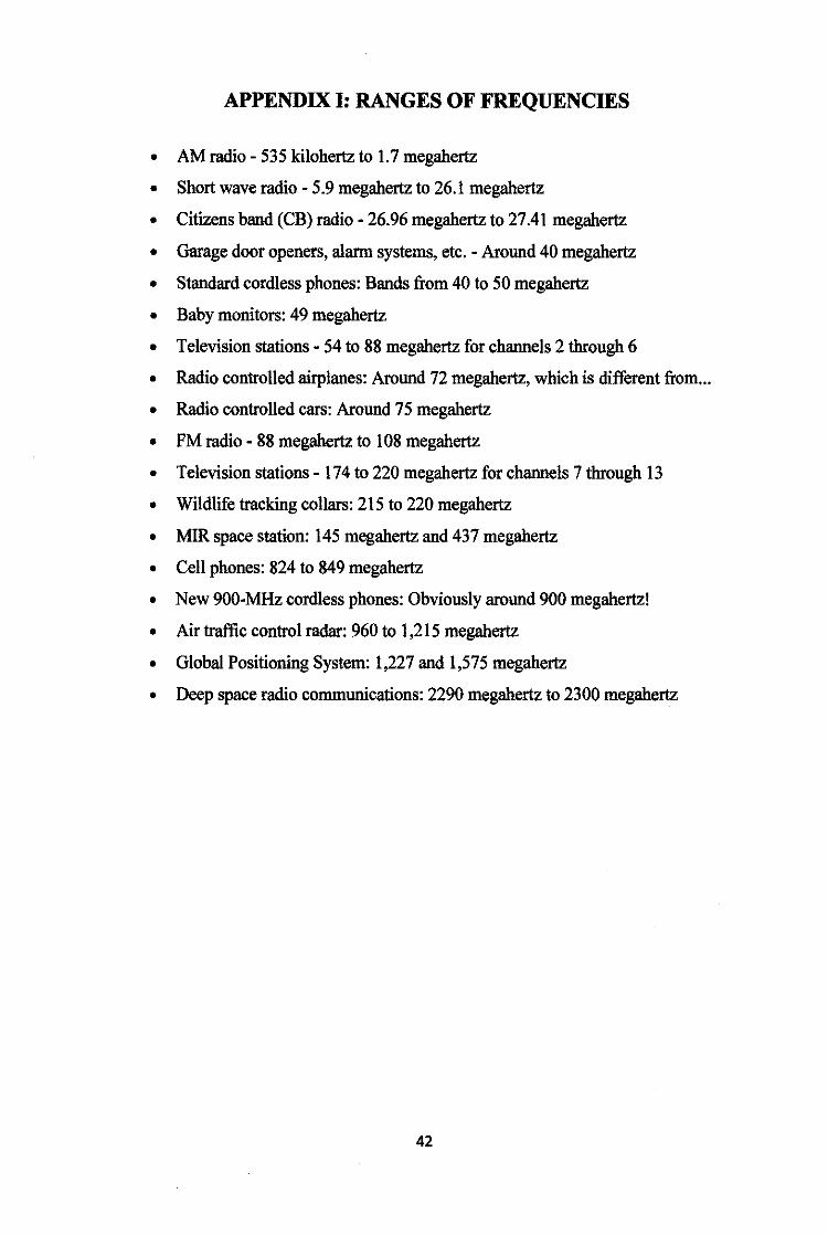
APPENDIX 1: RANGES OF FREQUENCIES
• AM radio - 535 kilohertz to 1. 7 megahertz
• Short wave radio - 5.9 megahertz to 26.1 megahertz
• Citizens band (CB) radio- 26.96 megahertz to 27.41 megahertz
• Garage door openers, alarm systems, etc. - Around 40 megahertz
• Standard cordless phones: Bands from 40 to 50 megahertz
• Baby monitors: 49 megahertz
• Television stations- 54 to 88 megahertz for channels 2 through 6
• Radio controlled airplanes: Around 72 megahertz, which is different from ...
• Radio controlled cars: Around 75 megahertz
• PM radio - 88 megahertz to I 08 megahertz
• Television stations- 174 to 220 megahertz for channels 7 through 13
• Wildlife tracking collars: 215 to 220 megahertz
• MIR space station: 145 megahertz and 437 megahertz
• Cell phones: 824 to 849 megahertz
• New 900-MHz cordless phones: Obviously around 900 megahertz!
• Air traffic control radar: 960 to 1,215 megahertz
• Global Positioning System: 1,227 and 1,575 megahertz
• Deep space radio communications: 2290 megahertz to 2300 megahertz
42

APPENDIX II: INTERNATIONAL STANDARDS
Currently, there is no specific rules and regulation for power-line
electromagnetic fields (electromagnetic field generated by electrical power
transmission). However, the standard can be derived from the regulations ruled out
for RF exposure.
The main characterizations in RF energy are its frequency and wavelength.
Based on the electromagnetic spectrum, RF waves have range from 3 kHz up to 300
GHz and the wavelength differ for each frequency based on the equation: speed of
light (c)= Frequency (t) X wavelength(/..). Fortunately, RF waves are among the
non-ionizing waves.
In measuring electromagnetic field, one of the most commonly unit used is
'power density'. It is used to measure a field that is far enough from the source.
Power density is described as power per unit area (e.g. m W /cm2, W /m2
).
Another criteria used to measure the RF energy is Specific Absorption Rate
or SAR. It is used to measure the quantity of RF energy that is being absorbed by
human body and the potential harm that it can bring. It is usually expressed in units
of watts per kilogram (W!Kg).
Besides that, the exposure time to RF radiation is another main criterion. It is
defined as a recommended time limit over an exposure. The concept is, exposure
level over time must not be greater than the allowable exposure limit (equal to power
density) multiply with the specified average time. As long as the exposure is not too
high or average, it is allowed to extend exposure time limit for a short period.
43

Frequency Electric Field Magnetic Field Power Density Averaging Time Range Strength (E) Strength (H) (S) IE P, I H p 01' s (MHz) (VIm) (Aim) (mW/cm2) (minutes)
0.3·1.34 614 1.63 (100)* 30 1.34·30 824/f 2.19/f (180/f)* 30 30·300 27.5 0.073 0.2 30 300·1500 f71500 30 1500·100,000 1.0 30
f = frequency in MHz *Plane-wave equivalent power density
Source: OET Bulletin 65, Edition 97-01, August 1997
Specific Absorption Rate (SAR)
OccupationaliConn·oUed Exposw·e General Uncontrolled/Exposure (100 kHz • 6 GHz) (100 kHz . 6 GHz)
< 0.4 Wlkg whole-body < 0.08 Wlkg whole-body
~ 8 Wlkg pat·tial-body ~ 1.6 W/kg partial-body
Source: OET Bulletin 65, Edition 97-01, August 1997
44

10
APPENDIX III: PROJECT MILESTONE
of Project Dissertation (Hard
• Project milestone -Process
45

APPENDIX IV: PROJECT GANTT CHART
• Milestone -Process
46

APPENDIX V: ANTENNA & RESONATOR
!.ANTENNA
The shapes and sizes of the antenna will depend on the frequency that the
antenna is trying to receive. The antenna can be a long, stiff wire to something like a
satellite dish. The size of an optimum radio antenna is related to the frequency of the
signal that the antenna is trying to transmit or receive. The reason for this relationship
has to do with the speed of light, and the distance electrons can travel as a result.
In one cycle of the sine wave, the transmitter is going to move electrons in the
antenna in one direction, switch and pull them back, switch and push them out and
switch and move them back again. In other words, the electrons will change direction
four times during one cycle of the sine wave.
For example, a radio station is transmitting a sine wave with a frequency of
680,000 hertz. That means every cycle completes in (1/680,000) 0.00000147 seconds.
One quarter of that is 0.0000003675 seconds. At the speed of light, electrons can
travel 0.0684 miles (0.11 km) in 0.0000003675 seconds. This means the optimal
antenna size for the transmitter at 680,000 hertz is about 361 feet (110 meters). For a
higher frequency, the time will be shorter, thus resulting in shorter antenna length.
47

2. RESONATOR
In a simple radio, a capacitor/inductor oscillator acts as the tuner for the radio.
Thousands of sine waves from different radio stations hit the antenna. The capacitor
and inductor resonate at one particular frequency. The sine wave that matches that
particular frequency will get amplified by the resonator, and all other frequencies will
be ignored.
In a radio, either the capacitor or the inductor in the resonator is adjustable.
Varying the capacitor changes the resonant frequency of the resonator and therefore
changes the frequency of the sine wave that the resonator amplifies. It is the same if
the inductor is varied. From this, it can be concluded that the value of both capacitor
and inductor have an effect in determining the resonant frequency.
48

aov
•ov
40V
20V
APPENDIX VI: SIMULATION RESULTS
Test 2: Stage capacitor (different value)
I I I I .. ' ' o I I I ' ' ' ' ' '
{A) 7Doubler.dat (active) I < > I ' . ' ' o o 1 I o I I I I 0 I I 1 o I >
I I ·I 0 I ,I I I < I 1- I I I I I I .I I I < 0 I I I I
·-~---:--·r··-:··· --~·--:···r·-~--- --:·"·-:---~--~-- --~·--:-··:--·r·· ···r·-~·--:---~-- --·:-··r---:··· -- --·:--- ---:···;·-:::: :::: ::::!''"~i'f"':::: ::::::
~~-~~:~t~:r~r:: :I~r:t~:t~~ :J::I:~t:I.-;B:~i~~ :::C:I:I::C~ ::I::t:I:: :: ::I:: ~~I:I:: l :·~. :::: :::: :::: :::: :::: ::::
::.~H::: ::l::.J:::l::i::: ::l::LH::_ ::U::Ll:: :::bU:::l:: :::H::Ll:: ::LH:::l:: ; ll9 •lJm.!•-1••! ;. ; ; ; ; ; ; ; ; ; ; ; ; ; ; ; ; ; ; ;
-- t··-:---~--~-~-i··· ··t··-:---~--1-- --~·--:---:-··t·· --·t··-:---:---~-- ---:--·t··-:---~-- ---:--·-t··-:---:--· : ; -'-r-:: : : : : : : : : : : : : : : : : : : : : : : ~ ,,,, ,,,, ..... ,_,,, '-''' ·''''
I I 1 I I 1 I I 0 I I I I I I I I I I I I I I I I I I I I I t I < I I I t I I I I I I I I I I I > o I I
I I I I I I I I I I I o o I I I I I I I I I I o o o 0
~ ~--·:-··t··-:~-- ··1----:···~·-1··· ··t··-:··-~--~--- --~·--:···}··t-- ---~---~---:---~-- ---}··t··-:··-~-- ---:---t-·"(---:---
-i-+++- -++++-- -++++-- --H---~--j-- --+-H+- -++++- -+-H-+r-r-~r-r-- --r-·r·r·r-- ·-r·r·r-r- ··r-r·-r--r· ---r-r··r·r· --r-~·-r·r-· ---r--r·r-·r·-• r r r • 1 , r , , • , , , r r , r r r r , r • • r r r > I I I 0 > r I I > > I I I I > I I I I I I I > I I I I
t··r--.r--1·-- ··j-··t··-r-·j··- --r---1·--r.--i·· ·· r-·t· --r-- t·· ---r--_-i···j·- -r-- ---r-.--r·--j-··r-- ---l·--r--t·· -r-· ··r·T·-r·r · ·· r-r··r·· r ·- ··r·r··r-·1-- ··r··r-~r-·r- -··r··.r-r··r·· ··-r··r--:~·-r- ---r·-r·r·-r--·i·--r- -r- ·1·-- -·1·-·t··r··-1--- -·t-·i··t ·1·· --;-- ;·--r ··t·· ---r·---;--t·· r·- ---r_-·t··;-··t·· · ·t -- !-·-t·r-·
ov- +-''---''--'-'--'-' -+-"'-'-' -'-' -'-' +-'"--'''-'''-''-!--"-'_.__._-+-"--'--'--'-+-'--'--'--'-+-'--'-"--'"-i I
eov
60V
40V
20V
Oe lOOma 200ma 300ms 400ms SOOma 600ms 700ma o V(C14:2)
Graph 1: Capacitor value = 1 nF
(A) 7Doubler.dat (active)
1 I o I I I t o o o t r r 1 t
' ' ' ' ' ' ' .. ' ' . ' ' ' I 0 0 I 0 0 I 0 0 0 0 I 0 0 0 I 0 I 0 I > 0 1 0 0 0 I 0 0 I• 0 I 1 I 1 I I I I I I I 0 I 1 I 1 I ...................................................................... ------~-- .. ····-- ___ ,. __ ............................ . I 0 0 0 I 0 I I 0 0 0 0 I 0 0 0 0 0 0 0 I I 0 0 0 0 0
: : -: Ui40 321m,iS.~97J : _: : : : : ·.: : : __ : : : : : : : : : : ··t·t··t-·1·-- --1-·Pf\·-- --!--1·--r---~-- --r--1·--r--r--- ---r--_1·-r·r-- ---r_-- ··1···t·· ··t··;-·._t·r--·-:·r- i i i i i i i i i i i i i i i i i ' : : i i i i
;J: : : : : : : : : : : : : : : : : : : : : : : : : : --~[--~- ·t··;--- --1-· r--~-- ;- -- ··t·-;---r- -~ --- --r --;---~ ··t·· --- i_·J ·t·-;-- ---r-- --t·- ;-- ---;--;--;---~-~- ---r--:r--?·-- --~-- -:---r---1··· --r.--i··-r- ·1··· -·t -- r--r --r-- ---r·--:1-·t --r-- · --r-· ··t·· r-- ---~--- r--?·--r--
• t t 1 {1~._2!l7nt,4J:.2 ) I, I '- 0 O 0 I 0 I I 0 I I I 0 0 I .o 0
• :-··:···t·•'l••• ·•~·••'••·L~•~•• ··:·•:···:-·:••• •·:·•:···:··t· •·•:·•:··:··:·· •·•:•• ··:·•·r-· •••:·•:••:··-:•· : : : : :· : : : : : : : : : : : : : : : :. : :
I t 0 I I I 0 1 I I I 0 I I I 0 0 I 0 0 0 I 0 0 0 0 0 I I I I 0 0 0 I 0 0 0 0 I 0 0 I I I 0 I I 0 I I 0 0 0 I I I I I I I I I o I 0 o I I I o ·I I I o o o I o o I
.;:::q::r: ::p:::q::: ::;::r;:r: :rrrr :::;::p:::;:: :::;:: ::r:;:: ::r;::r:;:: ' ' ' . ' --' ' -, ,. ' . ,• ' ' ' . ' ' ' . ' ' ' ' ' ., ' ·r ·r· -;--r-- --:-~-~---r -;--- --r-r -;·-r- -· :--;--·;-- r-· ---r---r--f·-·; ·- ---;-~ ·-r ·r-- ---:---r-;---~---o I I o o I I I o I I o I I I I 0 > o I o t o I I I I I I I I I I 0 I I 0 0 I I 0 1 I I I 0 I I 0 I I I
.:1:::~::;::;::: ::j::t::~::1::: ::;::;:::;::;::. ::;::;:::t::;:: :::;::;::;:::;:: :::r:: ::;:::;:: ::r:;::;:::t:: I 1 t I I I 0 '0 I• I 0' 0 I I 0 0 o- I 0 .I I 0 0 ,I I 0 0
· ·t·--r·-_t-·i· -- ··i···j··-r--1·-- -·!-·i··- r·-·1·-- --r--1·--r--t·· ---r--1 -- t··r-- ---r-· ··t -~r-- ··t -- ~--·1· -·r--ov ~~·__;•__;•_;.•-t~'_;_'~·~·-r~·~· ~· ~·~~·__;'__;'_;.'-+-'-'~·~· ...... ·-r-'-' ~-·~·~__;·_..;·~·..;'_;_'-1
Os lOOms 200m:~ 300ms 400IIIB SOOllUI 600JII8 iOOma o V{Cl4:2)
Iime
Graph 2: Capacitor value = 2.2 nF
49

eav
6W
.4W
20V
eov
6W
40V
zav
DV
' ' ' ' ' ' ' ' ' ' ' ' ' ' ' ' _, '
{A) 'iDoUbler.dAt {acti~)
I I I I I I I I
' ' ' ' ' ' ' ' ' ' ' ' I I I I
I I I I I I 1 I I 1 1 I I I I I I I I 0 0 I 0 I 0 I I 0 I I I I < I I I I I 0 < < < I I I < I I < I I < I I 0 < I I I I I I t I I I I < I t I I I < I < t. I I t I I t < , ~,-~-r-·t··r·· ~-r·r··r·r-~ ··r·r·-r.-·r·····r-·r-~r--!·· --·r··_r··r·r· ---r--r-1---;-- ··r··r·r··r-~ I I' I I, I I I I I I I I < I I > I I I I t I < I I I < I
-..!···:-. ·:-·. ~--. -- -:··-:-··:-·-·!··· . ·:-·· ~---~--~--- ---~- -~---~·-:·· . --~----~---:--· ~-- ---~· -~·--:··- ~-. ··-:-·- :-· _":" --:--· I I I I I -1 0 ,I I I t < I I < I I I I I I I 1' I 0 I -o I
·1·-+··.t--1~-- ··i-~+ ---~--~1--- --F-~- -+--+- · -~·-i--+ --i · · -- -~-~ 1---l----~ -- -- +-~ !---+--t-- --+--t--1·· +---• I I I 0 'I < I I < 0 I I I I I I I t I I I I I I t I I I 0 -, I I I I -1 I I I. I I I -, I I .t I -o 1- I ,- I I I I I
< I t I I I I I I I o I I I I t I I I I I I I I I I 0 I I I I I < I I < I I I I I I I I I I I I I I I < I I I I
.:J:::~::J::;::: ::JJ::~::J::: ::l::;:::t::J:: __ ::t::tr::: :::t::J::rr :::t::;::r:f:: ::r;::;:::r:: --;---r·-,·l--1·-· ··t--(·t··t·· ··t·;--·r·--t-- --_t-·1·--r--r-- ·--t~1--r-·t·· ···t--;-·r·t·· ·-r··r-·-i·--r·-
Oe lOOms 200I!l!l 300lllB 4CIOms SOOllll! 600'"' iOOms a V(C14:2)
Graph 3: Capacitor value = 4. 7 nF
{A) 7Doubler.dat {act-ive)
t 1 1 I I I I I I I I I I I I I I I t I ...................... _____ _, ....................................................... ,_ _______ ......................... .
O•
: :_ :. :. ( 7_7_,~532f·-6yr·o~:B_-) : : : : : : : : :. : :- ;__ :_. _: _; : --·t---~----~---~-- ----'.-··-:·-.--~ --:--- ---1---i---t---·t--· ---r---~---F.---r--- ---:----:----:-·--!·-· ----:---1··-·i---·t---
: : 1- : I---.,, I I I I I I o- I I I· I I I, I .1 _I I
..-::,: ···.·:, ---:·: --·.·: ••••• .:. .. ..:.~-~---~--- --~~---! .•• ! ..... ~- ... !. ••• ~ ... ~ ••• !. .......... .:. •• .:. •• ~ ••• ---~---~---L-.~---r· : : : : : : : : : : : : : : : : : : : :
: : : : : : : : : : : : : : : : ; : : : 0 I I I ..................... ' . ' ' I I t I I I I I
---r---r--·;---r~-
---r··r··r··-r·· ' ' ' ' ---r----r ·--r---r--
I I I I I I I 0
' . ' . ' ' ' ' --r--;--;--·i·-- -- ·i··-1--- t···t--- ---;·--t-- -r-- -r--- ---r--r--t-·1--~ -· ·i--·J··· i···t··---~---+·•i--·i··- ---~---1--··f--·f··· ---r- --r--·-t ---~--- ··t··-:--· ·-:-·· 1~-- ·--f--:i- ---i---t--·
: .: .: .-: : : -!. : : _: : : : : :. :. : : : : ---:-- ---:----:·. --:--- -- ·1-- --:---t· ··t··· ---~-- -~-. -~---:---- -- -:----:~~--:----:- ... ---:----:- .. ~---t--·
: : l l : : : : l : : : : ; : : ; -_: 1 1 . ' . ' . ' ' ' ' ' ' ' ' . ' ' ' ' . ' ' . ' ' ' ' ' ' --·:· ·--~:----:--·-:· -- ---~-- -~---: --·t ... ---~. --~---~---:-· ... --:----:--- --:-·. -:·-- ----:-- ·1·. -~-. ·t· .. I I I I ' I I I 0 ' I I ' I ' < I I I I I 1 1 I 1 I I 0 I t I I I 0 I I I I I t
I I I I I I I I I I 0 I I I I I I I I I I I ,< I .......... · ... ,_ ........ ----· ........ __ _, ___ ---·------·-··--·--- .............. ~-o--- ........ --- ........... - __ _,_ --~- ......... ..
I I I I I t I I o t < I I ! I I I < I I I I I I 0 1 1 1 1 1 1 0 1 1 0 1 1 I 1 I I I I I I I I I
~ --r-~-+~ ·+" -+-· -~+-"+-··\·-·+-- --_ .. i·· -·1--- t--~t--·- ---r-- --r-- ~r---r--- --+--+--+--+ ·· -- -1~---1·--1--~·t----• I ! I ! I I I I I I I I I I I I I I .!".-.. I I d <
' ' ' '
:::r:::~:::(:::r:: ----r:---r---r---r--
0.58 a V{C14:2)
' . ' ' . ' ' . ' ' ' ' ' I I I I o I I I I I 0 I ' ··+ --+--+· ·1·· . ... ~-. ·i·-- t··· t-·- . -·f· .. ~-. -~---t--. --+--+··+ --i--- ···i---i---i···~---
: : : : : : : : : : : : : : : : : : : : ---:-- ·-:--- o.:·· ·-:--- ~-- ~-- "1"". ~~- "! --- ·--f~ --~---~---:- --- -~·:-· ·-:-·- -:-· --:··· ... -:•~-~-- --:---~- .• : : : : : : : : : : : : : : : : : : : :
--+-- -:---~----:--- ----~-- -~-- .; .. .-; ... ---~- --~ --~~---~--- . -4---:..-. -{.·- -:--· ... -:---::. --~---;. •-" l l l 1 l 1 ! 1 1 : : : : 1 l 1 l 1 1 1
l-.08 1.58 2.08 2.58 3.0a
Graph 4: Capacitor value= 22 nF
50

!Al iDoubler.dat (active) eov ' .
o I I I .... ---~---~-- ...... I o o I
' ' ' ' ···t --+- -+---~-- ::r+::;:::;::: :::;:::;:::;:::;::: :::;:::;:::l:::~::: ::t:~t~~~~-t~ 4=tt::j::: -········: ... : .. r i , , ,
I I I I I I I t I I < I I I I I I I I ---- ____ ., ___ ..... ---~---·-- .. ---· --- -- ··--· ···-··· .... -- ........ -- .......... -- -............ ·---···· I I I o I I I o o I I I I I I I I ! I I
6UV ' ' ' ' I I o I
' ' ' ' : : : : : : : : : : : : : : l : : : l : ' . ' ' ' ' ' ' ' ' ' ' ' ' ' ' ' ' ' ' I I I 0 I I I I I < I o I I o I I I o I I o o I
---~- .............. "" -................. -- -- ...... ·---·- --· --- --- ·---·" --~- ..... -- .. ··- ..... " ........... -- ..... " .... ·--····. I I I I I 1 I I 0 1 I I I I I I I I I 0 I I I 0 I I o I I 1 1 1 I 0 I I I 1 I I I I I I I I I 0 I I I I I l I I I I I I I I I I I I 4 I I I I I
---r---r---r ---;·- ---~-··t --1-- ··1·· · ···1···1 · --r---·t··- --- r---r---r-- -r--- ··t· ·t·· ~---1--- --- 1--~--1- -~·i···t··· I 1 I I I I I I I I I I I I I I I I I I
4UV ---r· ·-r ---r·---r-- -··t· --r- -·;--· t- ---r-· r-· r-·· r·· ···r--r- --r··r··· · ·r· ·;-·-r --r -- ---r--r· ·r·-r-··
I I I I I I I I I I I I I I I I I I I I . . I I I I I I I I I o I I I o I I I < I I o I I I
---:----:-·-~--- ~- -- "--~--. ~-- ·t "" -t --- .. -~- .. }·· ·}---~- -- ---:----:-. ·-:--- ~- -- "--~--- ~---{- --·t-··
--+--+· -+-· +-- . --+ .. i-. --t-- -~ --- . --~-. -~---t ··+" -- -·+--+ ··+·- i- -- ---+"" i--. { ---t------r--·r·-r---r·· -··:. ··r·- -:··-·: --
"- -~-- ~t-·1- ---1--- ---1-- -1--~r ---r --- ---r---·r---r---r--- -- ·J-··-1-- ·1·--1--- --- i~--1·-·:t. ---r--· . ' ' ' -· ·r··-r- --r·--r ~-2UV I I I I I o o
' ' ' ' . . '
---r~--l---~- --r--- --·l···t- -1--- ·1--- --·1···1· --r- ··t··- --- r---r---r---r--- ---1--- ·J···t --1~-- ---1---1---1-- ·t· -----r--·r··-r··-r-- --r··r·-r--r-- ·--r--r··r··r-- ---r---r---r-·-r--- --r··r--T--r-- --·r··r--r--r-----}---:.-. -~-- -~-- ---:- --+· --:--- ~--- ·--~- -·~-- -t--- ;... --- r-- -~-- --r----~--- -. ..;.. .. -:--- -:---~--- ----:---i-·- ; ... ;- ·•
: : : : : : : : : : : : : : : : : : : : : : : ·l av ,, 0.5s 1. 0s 1.5a 2.as 2.Ss 3.0s
-D V{C14:2)_
Graph 5: Capacitor value= 47 nF
51