winter 2010 - electronics coolings3.electronics-cooling.com/issues/ecm_december2010.pdf · robert...
TRANSCRIPT

Volume 16, Number 4Winter 2010
ITEM PUBLICATIONS1000 Germantown pike, f-2plymouth meetinG, pa 19462-2486
chanGe service requested
presorted standardus postaGe paid
permit no. 225mechanicsburG, pa
www.electronics-cooling.com
Volume 16, Number 4
Open Bath ImmersIOn COOlIng In Data Centers
KeepIng mOOre’s law alIve
energy COnsumptIOn Of InfOrmatIOn teChnOlOgy Data Centers
www.electronics-cooling.com
InsIDe thIs Issue:semI-therm 27
aDvanCe prOgram


electronics-cooling.com ElectronicsCooling1
Editorial 2Resolutions
Robert Simons, Editor-in-Chief, Winter 2010 Issue
Thermal Facts and Fairy Tales 3 Fixed Temperature and Infinite Heatsinking
Jim Wilson, Associate Technical Editor
Calculation Corner 4
Thermal Interactions Between High-Power Packages and Heat Sinks, Part 1
Bruce Guenin, PhD, Associate Technical Editor
Feature Articles 10Open Bath Immersion Cooling In Data Centers: A New Twist On An Old Idea
Phil Tuma, 3M Company
Keeping Moore’s Law Alive 14Peter E. Raad, Southern Methodist University and TMX Scientific, Inc.
Energy Consumption of Information Technology Data Centers 28Madhusudan Iyengar and Roger Schmidt, IBM
Index of Advertisers 32
front coverData Center Cooling
Design by: Ann Schibik
contents
Symposium Snapshot ............................................................................. 20
SEMI-THERM 27 Committee Members .................................................. 21Program for Tuesday, March 22 .............................................................. 22
Program for Wednesday, March 23 ........................................................ 23Program for Thursday, March 24 ............................................................. 24
Hotel Information .................................................................................... 25Map of Venue ............................................................................................ 26
SEMI-THERM 27 Advance Program 19March 20-24, 2011, San Jose, California

2 ElectronicsCooling
Editorial BoardAssociate Technical Editors
Bruce Guenin, Ph.D.Principal Hardware Engineer
Clemens Lasance, IRPrincipal Scientist - Retired
Consultant at [email protected]
Robert SimonsSenior Technical Staff Member - Retired
Jim Wilson, Ph.D., P.E. Engineering Fellow Raytheon Company [email protected]
ResearcherGary Wolfe
Wolfe [email protected]
Published byITEM Publications
1000 Germantown Pike, F-2Plymouth Meeting, PA 19462 USA
Phone: +1 484-688-0300Fax: +1 484-688-0303
PublisherPaul Salotto
Content ManagerSarah Long
Business Development ManagerBob Poust
ReprintsReprints are available on a custom basis at
reasonable prices in quantities of 500 or more. Please call +1 484-688-0300.
SubscriptionsSubscription for this quarterly
publication is FREE.Subscribe online at:
www.electronics-cooling.com
All rights reserved. No part of this publication may be reproduced or transmitted in any form or by any means, electronic, mechanical, photocopying, recording or otherwise, or stored in a retrieval system of any nature, without the prior written permission of the publishers (except in accordance with the Copyright Designs and Patents Act 1988).
The opinions expressed in the articles, letters and other contributions included in this publication are those of the authors and the publication of such articles, letters or other contributions does not necessarily imply that such opinions are those of the publisher. In addition, the publishers cannot accept any responsibility for any legal or other consequences which may arise directly or indirectly as a result of the use or adaptation of any of the material or information in this publication.
ElectronicsCooling is a trademark of Mentor Graphics Corporation and its use is licensed to ITEM. ITEM is solely responsible for all content published, linked to, or otherwise presented in conjunction with the ElectronicsCooling trademark.
Produced by ITEM Publications
www.electronics-cooling.com
As you read this editorial we are fast approaching the end of another year. For some, this is a time for introspection. Who has not, at sometime, looked back at the past year in their personal life, maybe reflecting upon
what they accomplished, would have liked to accomplish, and what they did not accomplish? If you, the reader, are given to this type of reflection, I hope that you find satisfaction in what you have accomplished professionally and are not too disappointed in what you did not accomplish. If you are not given to this type of introspection, perhaps you should be. As engineers, many of us are subject to performance appraisals and project progress reports. This is an opportune time to conduct your own self-appraisal and consider what you might do to enhance your professional performance and satisfaction in the coming year.
On the occasion of the New Year, many people often make a New Year’s Resolu-tion to somehow improve their personal life. My objective here is to encourage you to reflect on your own professional situation and consider what you might resolve to do in the coming year, to enhance your engineering skills and knowledge, to make you an even better engineer and derive more satisfaction from your profession.
For example, you might consider furthering and broadening your engineer-ing knowledge by taking college courses at night or online towards an advanced degree in your discipline. Or you can conduct your own self-study program using the Internet as a resource. Just choose the topic or discipline you wish to explore and Google it. Having done this myself, I know that you will find many websites that are valuable sources of information on virtually any topic.
Another avenue you might choose is to consider sharing your knowledge or a recent technical accomplishment by writing a paper and presenting it at a technical conference. There are two IEEE-sponsored conferences totally devoted to electronics thermal management topics that you might consider. One is the Semiconductor Thermal Measurement and Management Symposium, commonly known as SEMI-THERM. This year’s SEMI-THERM will be held March 20-24 in San Jose, Calif. See Page 19 for the Advance Program. The other is the Intersociety Conference on Thermal and Thermomechanical Phenomena in Electronic Sys-tems, commonly, known as ITherm. ITherm is held every other year and is usually co-located with the IEEE Electronic Components and Technology Conference.
Of course, unless your company or organization is willing to pay for your at-tendance at a conference, this too can be an expensive proposition. However, there is still another avenue by which you can show off your work and that is through the trade press. Specifically, you might consider submitting an article for possible publication in ElectronicsCooling. We are always looking for articles that are tech-nically informative, interesting and maybe even provocative. You might consider submitting either a full-length feature article or a shorter length Technical Brief. Please feel free to contact any of the Associate Technical Editors (listed on this page) for more details.
So dear reader, I hope that you will give some thought to my suggestions and formulate your own professional resolution(s) for the coming year. I wish you suc-cess in whatever they may be. As for me and my colleagues on the editorial staff, we resolve to do our best in 2011 to continue to provide you the reader with the top-quality publication you have come to expect. l
Editorial
ITEM™
resolutions
Robert Simons Editor-in-Chief, Winter 2010 Issue
electronics-cooling.com ElectronicsCooling3
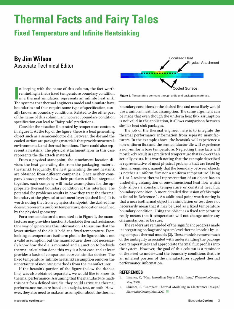
Localized HeatPhysical Attachment
Cooled Surface
Figure 1. Temperature contours through a die and packaging materials.
boundary conditions at the dashed line and most likely would use a uniform heat flux assumption. The same argument can be made that even though the uniform heat flux assumption is not valid in the application, it allows comparison between similar heat sink packages.
The job of the thermal engineer here is to integrate the thermal performance information from separate manufac-turers. In the example above, the heatsink will experience a non-uniform flux and the semiconductor die will experience a non-uniform base temperature. Neglecting these facts will most likely result in a predicted temperature that is lower than actually exists. It is worth noting that the example described is representative of most physical problems that are faced by thermal engineers, namely that the boundary between objects is neither a uniform flux nor a uniform temperature. Using a 1 or 2 resistor thermal representation of an object has an underlying assumption of one-dimensional heat flow which only allows a constant temperature or constant heat flux boundary condition. A more detailed discussion of this topic is found in Reference 1. An additional point worth noting is that a near isothermal object in a simulation or test does not necessarily mean that it may be used as a fixed temperature boundary condition. Using the object as a fixed temperature really means that it temperature will not change under any circumstances, so be sure.
The readers are reminded of the significant progress made in integrating package and system level thermal models by us-ing compact thermal models [2]. These models remove much of the ambiguity associated with understanding the package case temperatures and appropriate thermal flux profiles into the system. However, the goal of this column is a reminder of the need to understand the boundary conditions that are an inherent portion of the manufacturer supplied thermal performance information.
RefeRences1. Lasance, C, “Heat Spreading: Not a Trivial Issue,” ElectronicsCooling,
May, 2008.1. Shidore, S, “Compact Thermal Modeling in Electronics Design,”
ElectronicsCooling, May, 2007. l
In keeping with the name of this column, the fact worth reminding is that a fixed temperature boundary condition in a thermal simulation represents an infinite heat sink.
The systems that thermal engineers model and simulate have boundaries and thus require some type of specification, usu-ally known as boundary conditions. Related to the other part of the name of this column, an incorrect boundary condition specification can lead to “fairy tale” predictions.
Consider the situation illustrated by temperature contours in Figure 1. At the top of the figure, there is a heat generating object such as a semiconductor die. Between the die and the cooled surface are packaging materials that provide structural, environmental, and thermal functions. These could also rep-resent a heatsink. The physical attachment layer in this case represents the die attach material.
From a physical standpoint, the attachment location di-vides the heat generating die from the packaging material (heatsink). Frequently, the heat generating die and heatsink are obtained from different companies. Since neither com-pany knows precisely how their products will be integrated together, each company will make assumptions for the ap-propriate thermal boundary condition at this interface. The potential for problems results in how they treat the thermal boundary at the physical attachment layer (dashed line). It is worth noting that from a physics standpoint, the dashed line doesn’t represent a uniform temperature, its location is defined by the physical geometry.
For a semiconductor die mounted as in Figure 1, the manu-facturer may provide a junction to backside thermal resistance. One way of generating this information is to assume that the lower surface of the die is held at a fixed temperature. From looking at temperature isotherm plot in the figure, this is not a valid assumption but the manufacturer does not necessar-ily know how the die is mounted and a junction to backside thermal calculation done this way is a best case and at least provides a basis of comparison between similar devices. The fixed temperature (infinite heatsink) assumption removes the uncertainty of mounting methods from the manufacturer.
If the heatsink portion of the figure (below the dashed line) was also obtained separately, we would like to know its thermal performance. Assuming that the manufacture made this part for a defined size die, they could arrive at a thermal performance measure based on analysis, test, or both. How-ever, they also need to make an assumption about the thermal
Thermal facts and fairy Tales fixed Temperature and Infinite Heatsinking
By Jim WilsonAssociate Technical Editor

4 ElectronicsCooling Winter 2010
Substrate
Solder Bumps
Lid (Heat
Spreader)
2nd Level Interconnect
TIM1
TIM2
Air Cooled
Heat Sink
PCB Underfill Chip
Fig. 1a
requirements. Typically, higher power levels require higher conductivity fins with finer spacing, accompanied by a higher volumetric air flow than do lower power ones.
In years past, when power levels were lower, it became customary to calculate the junction temperature of the chip, TJ, using the following expression, assuming a simple series thermal resistance circuit [1, 2]:
TJ = P ∙ (ΘJC + ΘCS + ΘSA) + TA (1)where P is the dissipated power, ΘJC, ΘCS, and ΘSA are the junction-to-case, case-to-sink, and sink-to-air thermal resis-tances, respectively, and TA is the ambient temperature. [The term “case” refers to the top surface of the lid.] ΘJC is usually a test value furnished by the package vendor. ΘSA is normally based on the test value provided by the vendor. A complicating factor is that the heat sink vendors usually measure ΘSA with a uniform heat flux applied to the entire bottom of the base. In many applications, the heat sink is wider than the package, with the result that the vendor-supplied ΘSA values are lower than is appropriate for those applications. ΘSA is increased by the thermal resistance for heat to spread to the extremities of the heat sink base from the contact region with the packages. Fortunately, there is a relatively simple and accurate way to calculate this spreading resistance [3]. ΘCS is essentially the thermal resistance of the TIM2 material, calculated for a
T he need to accommodate increasing chip power has led to improved package and heat sink designs having much lower thermal resistance values than previously. This
has led to challenges in accurately calculating the thermal performance of the package and heat sink as an integral unit on the basis of thermal resistance measurements performed on each of them separately. Subtle heat transfer effects that can be neglected for lower-power packages become critical in the thermal analysis of high-power ones.
HigH-Power Package and HeaT SinkA typical configuration for a high power microprocessor or ASIC (Application-Specific Integrated Circuit) package at-tached to a heat sink is depicted in Figure 1a. This sort of flip-chip design lends itself to effective routing of power and signals between the chip and the PCB (Printed Circuit Board) below and to the efficient transfer of heat to the heat sink above. The package has a lid that is usually fabricated of copper to promote heat spreading. Thermal interface materials (TIMs) assist in the transfer of heat between the die and the lid (TIM1) and the lid and the heat sink base (TIM2). The heat sink base transfers the heat to the heat sink fin structure. Its thermal conductivity and thickness are chosen to suit the required power dissipa-tion. Obviously, higher power requires larger values of these parameters. The fin structure is also affected by the power
Thermal interactions Between High-Power Packages and Heat Sinks, Part 1
Bruce Guenin, PhD Associate Technical Editor
calculation corner
Figure 1. Diagrams of high-power package attached to a heatsink: a) a typical system application; b) simplified geometry as represented in the model. The fin structure is represented in the model by the application of an effective heat transfer coefficient to the top of the heat sink base.
a) b)
Lid (Heat
Spreader)
TIM1
TIM2
Heatsink
Base*
Surface of
Heat Generation Chip
Surface of
Heat Removal
Fig. 1b

6 ElectronicsCooling Winter 2010
specified bond-line thickness (BLT) and lateral dimensions bounding the region of significant heat flux. The calculated value of ΘCS is sensitive to the assumed area of this region.
This analysis ignores the presence of a secondary heat flow path to the ambient air through the PCB. This path is usually negligible for high-power packages because of the very low thermal resistance of the primary path to air via the heat sink. In lower power applications, neglecting this secondary path produces a conservative estimate of TJ.
The following analysis explores the effect of the thermal interactions between the package and the heat sink, specific to various applications, on the actual values of ΘJC, ΘCS, and ΘSA.
Modeling aPProacHFinite element analysis was conducted on a simplified solid model of the package and board as depicted in Figure 1b, using a commercial software tool [4]. The model represents only the chip-to-heat sink thermal path. Regarding the heat sink, only its base is explicitly represented in the model. The fin structure is accounted for by the use of an effective heat transfer coef-ficient, hEFF, applied to the top surface of the heat sink base [5, 6, 7]. All other surfaces are assumed to be adiabatic.
Table 1 lists the specific dimensions and material properties assumed for the package and heat sink. The lid and die widths of 40 mm and 13 mm, respectively, are typical for the sort of
applications under consideration. The heat sink was evaluated at three values of base width, wHS : 40, 70, and 100 mm. Three values of thermal conductivity, kHS, were assumed for the heat sink base: 166 and 240 W/mK, representing the lower and up-per bounds for aluminum alloys used in heat sinks, and 390 W/mK for pure copper. The heat sink base thickness, tHS, was set at 2 mm for the Al alloy designs and 6 mm for Cu. Values of hEFF , ranged from 50 to 2000 W/m2K, representing low-end heat sinks, with moderate air velocity, up to high-performance, folded-fin designs, at a high value of air velocity. The values of thermal conductivity chosen for TIM1 and TIM2 represent mid-range thermal performance. P is assumed to be 1W and TA to be 0˚C, in order to simplify the calculation of thermal resistances from the calculated temperatures.
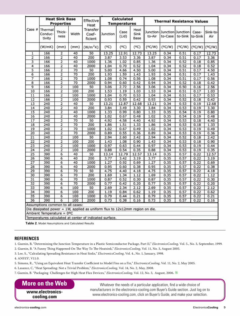
Model reSulTSTable 2 provides the calculated values of TJ, TCASE, and TSINKand the values of thermal resistances calculated from these temperatures and TA: ΘJA, ΘJC, ΘJS, ΘCS, and ΘSA for each of the 36 cases studied. The following discussion elaborates on each of these thermal metrics.
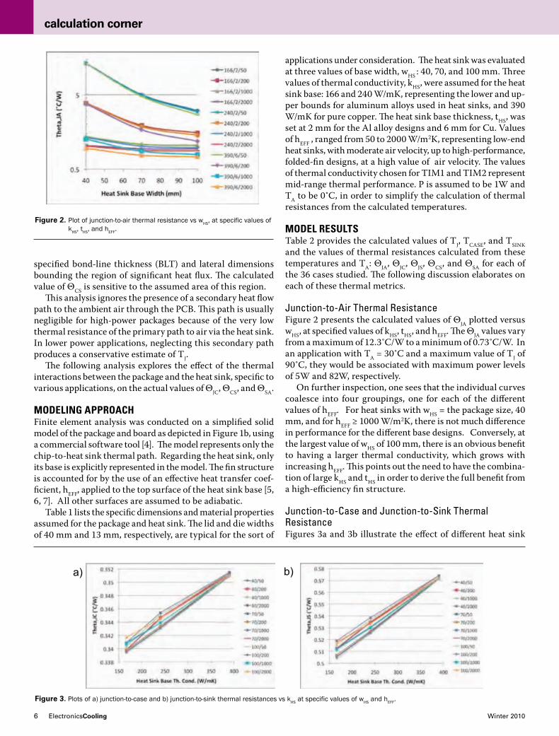
Junction-to-Air Thermal ResistanceFigure 2 presents the calculated values of ΘJA plotted versus wHS, at specified values of kHS, tHS, and hEFF. The ΘJA values vary from a maximum of 12.3˚C/W to a minimum of 0.73˚C/W. In an application with TA = 30˚C and a maximum value of TJ of 90˚C, they would be associated with maximum power levels of 5W and 82W, respectively.
On further inspection, one sees that the individual curves coalesce into four groupings, one for each of the different values of hEFF. For heat sinks with wHS = the package size, 40 mm, and for hEFF ≥ 1000 W/m2K, there is not much difference in performance for the different base designs. Conversely, at the largest value of wHS of 100 mm, there is an obvious benefit to having a larger thermal conductivity, which grows with increasing hEFF. This points out the need to have the combina-tion of large kHS and tHS in order to derive the full benefit from a high-efficiency fin structure.
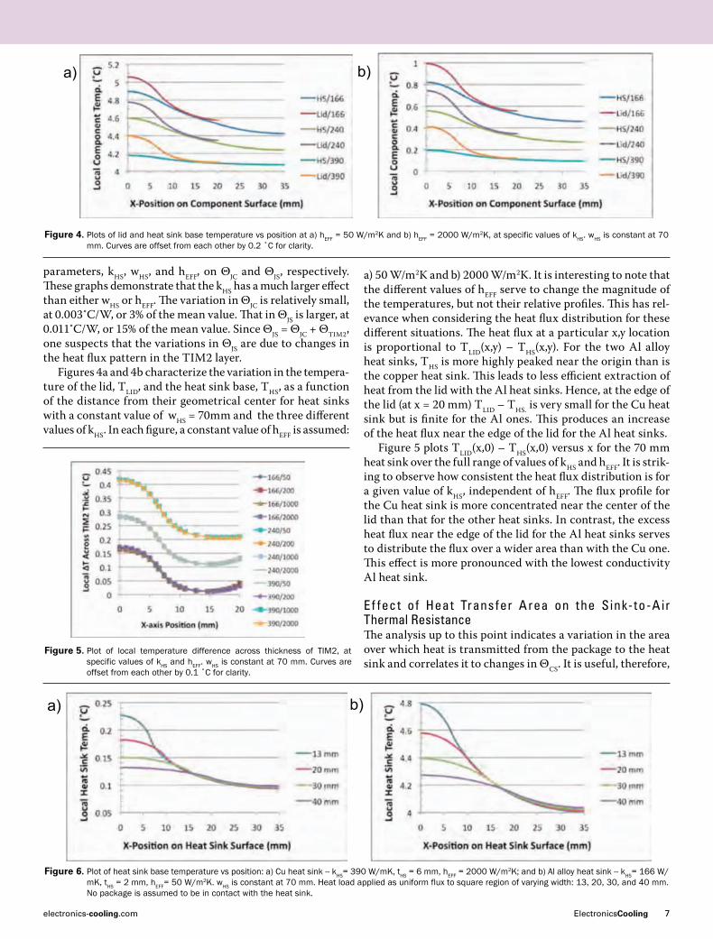
Junction-to-Case and Junction-to-Sink Thermal ResistanceFigures 3a and 3b illustrate the effect of different heat sink
Fig. 2
Figure 2. Plot of junction-to-air thermal resistance vs wHS, at specific values of kHS, tHS, and hEFF.
Fig. 3
a) b)
Figure 3. Plots of a) junction-to-case and b) junction-to-sink thermal resistances vs kHS at specific values of wHS and hEFF.
calculation corner
electronics-cooling.com ElectronicsCooling 7
parameters, kHS, wHS, and hEFF, on ΘJC and ΘJS, respectively. These graphs demonstrate that the kHS has a much larger effect than either wHS or hEFF. The variation in ΘJC is relatively small, at 0.003˚C/W, or 3% of the mean value. That in ΘJS is larger, at 0.011˚C/W, or 15% of the mean value. Since ΘJS = ΘJC + ΘTIM2, one suspects that the variations in ΘJS are due to changes in the heat flux pattern in the TIM2 layer.
Figures 4a and 4b characterize the variation in the tempera-ture of the lid, TLID, and the heat sink base, THS, as a function of the distance from their geometrical center for heat sinks with a constant value of wHS = 70mm and the three different values of kHS. In each figure, a constant value of hEFF is assumed:
Figure 6. Plot of heat sink base temperature vs position: a) Cu heat sink -- kHS= 390 W/mK, tHS = 6 mm, hEFF = 2000 W/m2K; and b) Al alloy heat sink -- kHS= 166 W/mK, tHS = 2 mm, hEFF= 50 W/m2K. wHS is constant at 70 mm. Heat load applied as uniform flux to square region of varying width: 13, 20, 30, and 40 mm. No package is assumed to be in contact with the heat sink.
Figure 4. Plots of lid and heat sink base temperature vs position at a) hEFF = 50 W/m2K and b) hEFF = 2000 W/m2K, at specific values of kHS. wHS is constant at 70 mm. Curves are offset from each other by 0.2 ˚C for clarity.
a) 50 W/m2K and b) 2000 W/m2K. It is interesting to note that the different values of hEFF serve to change the magnitude of the temperatures, but not their relative profiles. This has rel-evance when considering the heat flux distribution for these different situations. The heat flux at a particular x,y location is proportional to TLID(x,y) – THS(x,y). For the two Al alloy heat sinks, THS is more highly peaked near the origin than is the copper heat sink. This leads to less efficient extraction of heat from the lid with the Al heat sinks. Hence, at the edge of the lid (at x = 20 mm) TLID – THS. is very small for the Cu heat sink but is finite for the Al ones. This produces an increase of the heat flux near the edge of the lid for the Al heat sinks.
Figure 5 plots TLID(x,0) – THS(x,0) versus x for the 70 mm heat sink over the full range of values of kHS and hEFF. It is strik-ing to observe how consistent the heat flux distribution is for a given value of kHS, independent of hEFF. The flux profile for the Cu heat sink is more concentrated near the center of the lid than that for the other heat sinks. In contrast, the excess heat flux near the edge of the lid for the Al heat sinks serves to distribute the flux over a wider area than with the Cu one. This effect is more pronounced with the lowest conductivity Al heat sink.
Ef fect of Heat Transfer Area on the Sink-to-Air Thermal ResistanceThe analysis up to this point indicates a variation in the area over which heat is transmitted from the package to the heat sink and correlates it to changes in ΘCS. It is useful, therefore,
Fig. 4
a) b)
Figure 5. Plot of local temperature difference across thickness of TIM2, at specific values of kHS and hEFF. wHS is constant at 70 mm. Curves are offset from each other by 0.1 ˚C for clarity.
Fig. 5
Fig. 6
a) b)

8 ElectronicsCooling Winter 2010
to explore how the variation in this area will affect the value of ΘSA, the final stage in the heat flow path from the package to the air.
Figure 6 displays the results of FEA simulations in which heat is applied to a heat sink, not by way of a package in con-tact with it, but by applying a uniform flux over a square area of varying size, ranging from the die width (13 mm) to the package width (40 mm). This range represents the minimum and maximum conceivable area for heat transfer between the package and the heat sink. The graph quantifies the distribu-tion of THS(x) for a 70 mm wide heat sink. Figures 6a and 6b depict the “corner cases” representing maximum heat sink performance (6a) and the minimum performance (6b) studied for that value of wHS. Specifically, Figure 6a assumes the cop-per heat sink at hEFF = 2000 W/m2K and Figure 6b assumes the lower conductivity Al alloy heat sink at hEFF = 50 W/m2K. Varying the width of the heat transfer area (HTA) has the expected result on THS,PEAK. As the HTA width is reduced from 40 mm to 13 mm, THS,PEAK increases significantly. It is notable the change in ΘSA is most significant for the copper heat sink with the high value of hEFF. It is approximately equal to ± 0.05 ˚C/W about the mean value of 0.18˚C/W, or nearly ±30%, a significant effect. In contrast, for the Al alloy heat sink with the relatively low value of hEFF, the variation in ΘSAis only ± 0.3˚C/W or ± 5%. This should not be surprising since the low value of hEFF ensures that the convective contribution to the total value of ΘSA will be much larger than the conduc-tive contribution.
It is desirable to develop a metric for quantifying the HTA. The method developed herein is as follows:• Calculate ΘSA for each of the 36 heat sink-hEFF configuration,
applying a uniform heat flux at each of four values of HTA width (13, 20, 30, and 40 mm).
• Perform regression analysis to fit each ΘSA vs HTA width curve to a 3rd-order polynomial. The polynomial can ac-curately predict the ΘSA at an arbitrary value of HTA width within the specified 13 -40 mm range.
• Use a spreadsheet solver to determine the value of HTA width for each of the 36 configurations to produce a value of ΘSA equal to the value of ΘSA reported in Table 2 for the integrated package + heat sink simulations.Figure 7 shows the values of HTA width calculated in this
fashion plotted versus kHS for all values of wHS and hEFF evalu-ated. They range from 17 to 24 mm. It shows that both kHS and wHS have a significant effect on the HTA width. The largest value of HTA width occurs for the smallest value of kHS and the largest value of wHS.
The resultant values of HTA width can be used in the ap-plication of analytical methods to predict ΘJA. For example, it could be used to calculate ΘCA = ΘTIM2 by providing an area that, when multiplied by the total power, would yield approxi-mately the same value of TLID – TSINK as that obtained using the original FEA approach.
In light of these findings, it is worthwhile to revisit the comments made at the beginning of this article regarding calculating a spreading resistance term to correct the vendor-supplied ΘSA values when the heat sink is larger than the pack-age. In performing these calculations, it is common practice to assume a uniform heat flux from the package into the heat sink over the full package width. It is now clear that applying this assumption to a ΘSA calculation for a high-performance heat sink, such as the one of Figure 6a, will likely generate a significant underestimate of ΘSA.
Preview of ParT 2Part 2 of this article will address the ultimate objective of this study: to evaluate plausible methods for predicting ΘJA for an integrated package-heat sink configuration on the basis of test results obtained for the package and heat sink separately. It will leverage both the physical insights developed in the course of this analysis as well as the specific values of HTA in this next exercise.
Figure 7. Plot of heat transfer area width vs kHS at specific values of wHS and hEFF.
Fig. 7
Table 1. Model Dimensions, Materials and Properties
Table 1
calculation corner
electronics-cooling.com ElectronicsCooling 9
Table 2. Model Assumptions and Calculated Results
Table 2
referenceS1. Guenin, B, “Determining the Junction Temperature in a Plastic Semiconductor Package, Part II,” ElectronicsCooling, Vol. 5., No. 3, September, 1999.2. Guenin, B. “A Funny Thing Happened On The Way To The Heatsink,” ElectronicsCooling, Vol. 11, No. 3, August 2005.3. Lee, S., “Calculating Spreading Resistance in Heat Sinks,” ElectronicsCooling, Vol. 4., No. 1, January, 1998.4. ANSYS®, V11.0.5. Simons, R., “Using an Equivalent Heat Transfer Coefficient to Model Fins on a Fin,” ElectronicsCooling, Vol. 11, No. 2, May 2005.6. Lasance, C, “Heat Spreading: Not a Trivial Problem,” ElectronicsCooling, Vol. 14, No. 2, May, 2008.7. Guenin, B. “Packaging Challenges for High Heat Flux Devices,” ElectronicsCooling, Vol. 12, No. 3, August, 2006. l
www.electronics- cooling.com
Whatever the needs of a particular application, find a wide choice of manufacturers in the electronics-cooling.com Buyer’s Guide section. Just log on to
www.electronics-cooling.com, click on Buyer’s Guide, and make your selection.
More on the web

10 ElectronicsCooling Winter 2010
T he inefficiencies of legacy datacenter air cooling schemes are by now well known. New “Free Air” cooling technolo-gies in which air is introduced to the racks in a facility
or container and confined in hot and cold plena probably represent the pinnacle of air cooling efficiency, at least where climate permits them. However, development of an air cooled server requires significant engineering resources. The resul-tant solution is hardware intensive and the power density and energy efficiency are ultimately limited by airflow paths, fans, blowers, filters and the inherent inability to capture and utilize the waste heat. This suggests an inefficient use of engineering and natural resources, electrical power, and real estate [1].
It is generally recognized that liquid cooling can dramati-cally increase efficiency, power density and the thermodynamic availability of the heat removed [2]. However, implementation of traditional pumped liquid cooling schemes, be they single- or two-phase, is also hardware intensive. These systems bear the inherent costs of cold plates, manifolds, redundant pumps, plumbing, controls, heat exchangers, quick disconnects (QDs), etc. Controlling the flow and mitigating the loss of water or refrigerant through this myriad of components within a rack or container is an engineering challenge exacerbated by the num-ber and variety of heat generating devices on a server and the requirement that each server within a rack be “hot swappable.” It is for these reasons that liquid cooling has been relegated to the world of mainframes and supercomputers, the cost barri-ers too high for the commodity datacom environment to bear.
Passive two-phase immersion cooling is arguably one of the most elegant ways to capture all of the heat generated by a complex electronic assembly. By immersing electronics in a bath of volatile dielectric coolant that boils on the heat gen-erating devices, much of the aforementioned hardware can be eliminated. The heat is captured efficiently as saturated vapor and can be transferred efficiently by condensation to an external heat sink like air or water. This technique has been used for decades in countless transformers, klystrons and traction inverters, some of which are still in production today being favored for their simplicity, reliability, power density and performance. However, these systems use sealed pressure vessels with hermetic electrical connections. Since they are evacuated and filled like refrigeration systems, they are not easily serviced. Creating and maintaining such an enclosure for commodity computational or communications hardware that
Phil Tuma is an Advanced Application Development Specialist in the Electronic Mar-
kets Materials Division of 3M Company. He has worked for 15 years developing
applications for fluorinated heat transfer fluids in various industries. His current work is
focused on developing techniques that facilitate the use of passive 2-phase immersion
for cooling power electronics and datacom equipment. He holds a BA from the
University of St. Thomas, a BSME from the University of Minnesota and a MSME
from Arizona State University.
Open Bath Immersion Cooling In Data Centers: A New Twist On An Old IdeaPhil Tuma 3M Company, St. Paul, Minnesota

electronics-cooling.com ElectronicsCooling 11
must be field serviceable is challenging. It is for these reasons that two-phase immersion cooling too has been relegated to the world of supercomputers and most engineers dismiss the idea of immersion cooling within a data center.
However, immersion cooling can be applied without the aforementioned complexities resulting in a system that is not only elegant but simpler, more dense, much less expensive and at least as efficient as any other liquid cooling technique. This new twist on passive 2-phase immersion cooling was detailed in a recent publication [3].
OpeN BATh ImmersION COOlINg CONCepT (OBI)In this concept, servers are immersed side-by-side in simple mod-ular semi-open baths of a volatile dielectric fluid (Figure 1). The term “semi” denotes a bath that is closed when access is not needed much like a chest-type food freezer. Unlike more traditional im-mersion systems, these baths operate at atmospheric pressure and have no specialized hermetic connections for electrical inputs and outputs. Instead, electrical connections from a submerged backplane enter a simple conduit beneath the liquid level and exit the top of the tank. The only other opening is through a vapor trap as will be discussed. The vapor generated by boiling rises to a condenser integrated into the tank and cooled by tower water or water used at some distance for comfort heating. Alternatively, the vapor can flow passively to an outdoor natural draft or forced air condenser to transfer its heat to outdoor air without water as an intermediate. Condensed vapor simply falls back to the bath. Servers can be hot swapped without disturbing their neighbors by simply removing them from the bath. They exit the bath dry
resulting in minimal and easily quantified fluid losses.Among the advantages of OBI compared to more tradi-
tional liquid cooling schemes, is the fact that all server- and
NOmeNClATUre
h Heat transfer coefficient [W/m2-K] or [W/cm2-K]
P Pressure [Pa]
Q Power [W]
Q” Heat flux [W/cm2]
R Thermal resistance [°C/W], [°C-cm3/W]
ρ Density [kg/m3]
T Temperature [°C] or [K]
sUBsCrIpTs
atm atmospheric
b boiling or boiling point
c chip
cond condenser or condensation
f fluid
i initial or inlet
j junction
o final or outlet
s sink
sat fluid saturation
t cold trap
w water
12 ElectronicsCooling Winter 2010
most rack-level cooling hardware are eliminated along with considerations relating to their integration, reliability and power consumption. Isothermal operation and fire protec-tion are intrinsic to the technology. Of course, there are other considerations.
ChIp-TO-FlUID perFOrmANCeThe system thermal performance has two components. The first is quantified by considering the junction-to-fluid temperature difference of the central processing unit (CPU). A typical CPU package is almost ideally suited for passive 2-phase immersion cooling. It requires only the addition of a 100μm thick porous metallic boiling enhancement coating (BEC) to the integrated heat spreader (IHS). These coatings produce boiling heat trans-fer coefficients, h>10 W/cm2-K at heat fluxes exceeding 30W/cm2. Incorporating this technology directly onto the IHS dur-ing package assembly eliminates the secondary thermal inter-face common to many liquid cooling schemes without altering the package assembly process. The IHS not only spreads the heat, to reduce the flux to a manageable level, but it protects the chip beneath from fluid-borne contaminants.
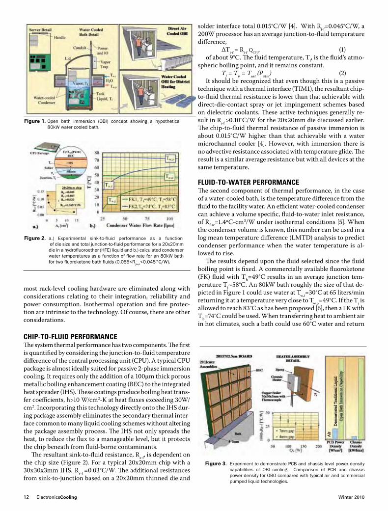
The resultant sink-to-fluid resistance, Rs-f, is dependent on the chip size (Figure 2). For a typical 20x20mm chip with a 30x30x3mm IHS, Rs-f =0.03°C/W. The additional resistances from sink-to-junction based on a 20x20mm thinned die and
solder interface total 0.015°C/W [4]. With Rj-f=0.045°C/W, a 200W processor has an average junction-to-fluid temperature difference,
ΔTj-f = Rj-f QCPU, (1)of about 9°C. The fluid temperature, Tf, is the fluid’s atmo-
spheric boiling point, and it remains constant. Tf=Tb=Tsat(Patm) (2)It should be recognized that even though this is a passive
technique with a thermal interface (TIM1), the resultant chip-to-fluid thermal resistance is lower than that achievable with direct-die-contact spray or jet impingement schemes based on dielectric coolants. These active techniques generally re-sult in Rj-f >0.10°C/W for the 20x20mm die discussed earlier. The chip-to-fluid thermal resistance of passive immersion is about 0.015°C/W higher than that achievable with a water microchannel cooler [4]. However, with immersion there is no advective resistance associated with temperature glide. The result is a similar average resistance but with all devices at the same temperature.
FlUID-TO-WATer perFOrmANCeThe second component of thermal performance, in the case of a water-cooled bath, is the temperature difference from the fluid to the facility water. An efficient water-cooled condenser can achieve a volume specific, fluid-to-water inlet resistance, of Rf-w=1.4ºC-cm3/W under isothermal conditions [5]. When the condenser volume is known, this number can be used in a log mean temperature difference (LMTD) analysis to predict condenser performance when the water temperature is al-lowed to rise.
The results depend upon the fluid selected since the fluid boiling point is fixed. A commercially available fluoroketone (FK) fluid with Tb=49°C results in an average junction tem-perature Tj~58°C. An 80kW bath roughly the size of that de-picted in Figure 1 could use water at Tw,i=30°C at 65 liters/min returning it at a temperature very close to Tw,o=49°C. If the Tj is allowed to reach 83°C as has been proposed [6], then a FK with Tb=74°C could be used. When transferring heat to ambient air in hot climates, such a bath could use 60°C water and return
Figure 2. a.) Experimental sink-to-fluid performance as a function of die size and total junction-to-fluid performance for a 20x20mm die in a hydrofluoroether (HFE) liquid and b.) calculated condenser water temperatures as a function of flow rate for an 80kW bath for two fluoroketone bath fluids (0.055<Rjw,o<0.045°C/W).
Figure 3. Experiment to demonstrate PCB and chassis level power density capabilities of OBI cooling. Comparison of PCB and chassis power density for OBO compared with typical air and commercial pumped liquid technologies.
Figure 1. Open bath immersion (OBI) concept showing a hypothetical 80kW water cooled bath.

electronics-cooling.com ElectronicsCooling 13
it at 73°C, temperatures hot enough to eliminate the need for cooling tower water in the hottest climates. If instead water is used for comfort heating, the water flow rate could be reduced to about 26 liters per minute. The bath would accept 30°C water and return it to the heating system at ~74°C (Figure 2).
A NOTe ON pOWer DeNsITyPower density within a server chassis has historically been limited by airflow and plumbing considerations. The density of a typical air cooled server chassis is 0.04kW/liter versus 0.16kW/liter for a hybrid air/water supercomputer node [2]. An OBI-cooled server has no cooling hardware. Determining how densely the remaining electronics could be packaged is beyond the scope of this work but it is worthwhile explor-ing what power density could be cooled by immersion. The simulated printed circuit board (PCB) shown in Figure 3 holds 20 heater assemblies comprised of 19x19mm 200W ceramic heaters epoxy bonded on one side to 30x30x3mm BEC copper heat spreaders that simulate a modern IHS. A thermocouple in the fluid, Tf, and one within each heat spreader, Ts, permit calculation of the individual thermal resistances.
This PCB was immersed in a confined vertical channel of the same area as the board with 4 and 7mm gaps between the boiling surface and the adjacent wall. This assembly was able to dissipate 4kW (200W per heater assembly) for a 4mm gap when the bath was filled with C3F7OCH3, a hydrofluoroether working fluid. The average Rs-f are shown in Figure 3, bracketed by ½ standard deviation on each side. 4kW equates to a PCB level heat flux of 11.7W/cm2 versus 1.7W/cm2 for the Cray X1E spray-cooled supercomputer [7]. These data suggest that 4kW/liter with <100cc of fluid per kW are certainly attainable, if only from a thermal point of view. This fluid fill cost is less than the cost of copper used in two 2U heat sinks and the potential for reduction of materials and waste associated with PCB manu-facture is significant.
FlUID lOssesSome fluid loss is intrinsic to the technology and this affects not only the cost of ownership but also the greenhouse gas emis-sions and the likely human exposure in the datacenter. However, the loss mechanisms are well understood and easily mitigated because they act at one point above the vapor zone of a bath which is at atmospheric pressure. One can contrast this with a
conventional pumped loop with its myriad of braze joints, con-nectors and seals that are wetted and under positive pressure.
Losses are most pronounced during commissioning and startup of a new bath when air dissolved in the fluid and present in the head space are purged bringing vapor with them. Losses during operation are limited to diffusion through the IO conduit and those associated with daily power fluctuations which cause the vapor zone to rise (expelling more air/vapor) and fall. By venting the exiting air/vapor stream through an on-demand, thermoelectrically cooled condenser or “trap” most of the vapor within it can be condensed and returned to the system.
The resultant annual losses depend on this trap temperature, Tt, and can be easily calculated. Assuming Tt=10°C and one 25% load fluctuation per day, the annual fluid consumption cost for the 80kW bath mentioned earlier is $123/yr at the typical fluid list price. This compares favorably with the $184/yr cost of operating rack level pumps in a traditional liquid cooling system at $0.05/kWh and the $2,800/yr cost of operating just the server fans in a typical air-cooled rack assuming they use 80W per kW of server power. If a fluoroketone working fluid with a global warming potential (GWP) of 1 is used, the green-house gas emissions resulting from annual fluid loss are 0.2% of those associated with operating rack pumps that produce 7.18x10⁻⁴ metric tons CO2/kWh.
CONClUsIONsIt has been said that datacenter operations are all about cost, cost, cost. Its costs money to develop, manufacture, house and operate a thermal management solution. Less tangible environ-mental costs like greenhouse gas emissions, natural resource consumption and e-waste are becoming increasingly important to society. Open bath immersion (OBI) cooling technology appears able to have a dramatic effect on both financial and environmental costs in all stages of a server’s life cycle (Figure 4). Its investigation continues through long term demonstra-tions that will track thermal performance, serviceability, fluid health, fluid loss, etc.
reFereNCes1. Shah, A., Christian, T., Patel, C., Bash, C., Sharma, R., “Assessing ICT’s
Environmental Impact,” Computer, 42(7), pp. 91-93, July 2009.2. Ellsworth, M., and Iyengar, M., “Energy Efficiency Analyses and Comparison
of Air and Water Cooled High Performance Servers,” IPACK2009-89248, July 19-23, San Francisco, CA.
3. Tuma, P.E., “The Merits of Open Bath Immersion Cooling of Datacom Equipment,” Proc. 26th IEEE Semi-Therm Symposium, Santa Clara, CA, Feb. 21-25, 2010.
4. Colgan, E.G., et al, “A Practical Implementation of Silicon Microchannel Coolers for High Power Chips,” 21st IEEE Semi-Therm Symposium, San Francisco, California, March 2005, pp. 1-7.
5. Barnes, C.M. and Tuma, P.E., “Practical Considerations Relating to Immersion Cooling of Power Electronics in Traction Systems,” Proc. 2009 IEEE Vehicle Power and Propulsion Conference (VPPC’09), Sept. 7-10, pp. 614-621.
6. http://www-03.ibm.com/press/us/en/pressrelease/32049.wss7. Pautsch, G., “Thermal Challenges in the Next Generation of
Supercomputers,” Presentation, CoolCon 2005, May 16-17.
Figure 4. Comparison of projected costs associated with a server’s thermal management solution as a function of life cycle.

14ElectronicsCooling Winter 2010
A recent news item [1] described the intended eff orts of researchers from IBM, EPFL, and ETH to “keep Moore’s Law for another 15 years.” Doing so, the article adds,
“will require a change from mere transistor scaling to novel packaging architectures such as so-called 3D integration, the vertical integration of chips.” Th e four-year collaborative project called CMOSAIC will investigate cooling techniques that can support a 3D architecture, including “the use of hair-thin, liquid cooling microchannels measuring only 50 microns in diameter between the active chips.” Th e research-ers from industry and academia will undoubtedly use myriads of experimental and computational methods to devise their approaches, design their solutions, construct their prototypes, and ultimately test the merits of their hypotheses. Th is is consistent with what we have always done! However, the inevitability of three-dimensionality in integrated circuits [2] raises an interesting question: how will we know what’s happening inside? Whether it is physicians diagnosing and mapping optimal routes for successful surgery or authorities interested in the activities of a suspect operating within the inner confi nes of a large structure, the problem is the same: how to assess what we cannot access.
Engineers and scientists have long relied on measurements to diagnose system behavior, enlighten thinking, and guide next steps. Th e dramatic advances in computing machines have made it possible to add numerical simulation as a power-ful contributor in our arsenal of investigatory tools for complex systems. Traditionally, though, an individual researcher’s strength would favor one approach over another. More recently as computers have become more potent and software packages have become more accessible, experimentation has become in the minds of some only necessary in so far as it provides valida-tion to numerical models. But the community knows too well the dangers of single-minded approaches to any signifi cant problem at hand. Th e question is then not whether we need to leverage as many individual approaches as possible — ana-lytical, experimental, and computational — but rather which ones are most appropriate to solve our particular problem at hand, which is to fi gure out the thermal behavior of buried electronic devices and features of interest. Th is is not an idle question on the semiconductor roadmap. Without a view into the inner workings of complex devices, we will be blind to the actual performance of our designs, and hence condemned to spending our valuable time and energy on trial-and-error rather than rapid prototyping and iterative refi nement.
Let us fi rst consider experimentation as it pertains to this discussion. A measurement has the most important advan-
Keeping Moore's Law Alive
PeterE.RaadiscurrentlyaFullProfessorofmechanicalengineeringatSMUandholdstheLindaWertheimerHartProfessorship.
Hehasreceivedseveralteachingandresearchawards,includingtheASME
NorthTexasSectionEngineeroftheYearin1999-2000,andtheHarveyRostenAward
forExcellencein2006.HereceivedhisPh.D.inmechanicalengineeringfromtheUniversityofTennesseeatKnoxvillein1986.Hehaspublishedover50articlesandgivenover100conference
andinvitedtalks.HeisaFellowofASMEandSeniorMemberofIEEE.
Peter E. RaadSouthern Methodist University and TMX Scientific, Inc., Dallas, Texas


16ElectronicsCooling Winter 2010
tage of capturing the actual thermal behavior with all the physics as well as the geometric and material complexities that are influencing the operation of a real device. However, the Zeroth Law of Thermodynamics confines us to having to measure temperature indirectly by calibrating the response of a third body to differing temperature levels. There are a number of useful approaches [3, 4], which can be categorized based on the relationship between the measuring implement and what is being measured. We may speak of invasive and non-invasive, contact and non-contact approaches, and within these, we can refer to methods that rely on material behavior (e.g., mercury thermometer, liquid crystal paint), electrical response (e.g., thermocouples, thermistors), optical signature or interference (e.g., infrared, thermoreflectance), to name but a few. Different methods have different strengths, limita-tions, and figures of merit, e.g., accuracy, resolution (spatial, temporal, and temperature), and precision. Irrespectively, for an implement to record the temperature of a material, the two have to be communicant either physically or optically. Physical contact presents the difficulty of isolating the effect of contact itself, whereas an optical approach limits access to surface or near-surface regions. Given the above, one can now certainly appreciate the challenges of measuring vertically integrated electronic devices, and without even yet consider-ing the additional difficulties presented by the ranges of scales from nanometers to centimeters that are inherent in modern complex devices. Access is a limiting factor.
Computational approaches, on the other hand, do not have issues of physical or optical access. Given a choice of spatial discretization (e.g., finite element/volume/difference) and temporal discretization (e.g., explicit, implicit, trapezoidal), an analyst can construct the computational domain of interest, select the heat transfer physics in play, prescribe initial and boundary conditions, and then wait for the numerical simula-tion to complete. Of course, (i) different numerical approaches have differing levels of accuracy, stability, and convergence; (ii) numerical simulations cannot represent physics that are not included in the formulation; and (iii) geometric and mate-rial complexities can make grid generation quite challenging. The power of computations is that, given an accurate and appropriately convergent solution, we can easily extract the thermal behavior of important features wherever they may be within the computational domain. However, even the most precise and accurate numerical simulations cannot give us results that exceed the fidelity of the input data, be they those associated with the geometry, the material properties, or the heat sources. This is an important point. Numerical simula-tions can give us gloriously colorful representations of thermal behavior, but only as it pertains to the idealized representation of the device as described by the input data. The numerical results do not automatically comprehend the effects of data uncertainty, natural device aging, or rapid deterioration due to device malfunction. Input data are a limiting factor.
So, on the one hand, experiments can comprehend physics and device complexity, but are restricted to specific locations, and on the other, numerical simulations can provide detailed, transient, 3D behavior, but only insofar as the input data repre-sent the actual device of interest. What if we didn’t have to pick sides? What if we could marry the two approaches to overcome
their respective limitations? Consider the notion of what we might call “tuning approaches” that leverage experimental data to guide simulation. This concept is not unique to ther-mal analysis of semiconductor devices. In a slightly different approach, perhaps better termed “data assimilation,” meteo-rologists begin by predicting the path of a hurricane starting with a reasonable input data set, but continually modify the progress of the simulation as actual data become available. For our problem at hand, one could imagine simulating a vertically integrated device with the best possible available input data, but then comparing the results in those locations and areas where physical measurements are available in order to generate a more representative input data set. Such an iterative process (Fig. 1) would continue until computations and measurements agree to within an acceptable error [5].
There are two important issues to consider: uniqueness and feasibility. First, when solving partial differential equations, particularly if they are nonlinear, it is possible, even probable to have multiple scenarios yield the same temperature value at some given point. Just because the computational and experimental results agree at one point does not make the solution unique. From an information entropy point of view, however, as the number of points involved in the comparison increases, the probability of uniqueness increases consider-ably. Indeed, as the number of reference points increases into the hundreds and thousands, the probability of two different well-posed problems producing matching results at all those points becomes infinitely small. Secondly, in order for such an iterative approach to be practical, the numerical simulation has to be very fast. The computational time depends on the chosen resolutions in space and in time as well as on the efficiency of the numerical algorithms used to solve the resulting systems
Figure 1. Iterative cycle to optimize input data subject to agreement with experimental data.
electronics-cooling.com ElectronicsCooling17
of equations. Setting aside algorithmic efficiency and computer speed, the overall time budget is primarily driven by grid size and time step. A difficulty particular to the thermal model-ing of integrated circuits is the range of spatial and temporal scales that must be resolved in order for the simulation to be useful. If the smallest grid size were chosen to be larger than the smallest heat source, the effect of the latter would be lost. If, on the other hand, the smallest geometric and thermal features are appropriately resolved, the problem size can be-come prohibitively large, making multiple solutions within an optimization approach impractical.
Compact models [6] and ultra-fast numerical approaches [7] have been introduced to reduce computational time by orders of magnitude. Analysts who have at their disposal ultra-fast simulation capabilities become more likely to practice itera-
tive refinement and even experimentally-guided optimization. Additionally, this opens up the interesting possibility of inte-grating sensors that not only measure locally but also predict thermal behavior in other regions of interest. So then even beyond design and prototyping, highly optimized thermal simulation codes could be embedded within small chips to continually predict internal thermal behavior within operating devices and provide feedback to alter their behavior.
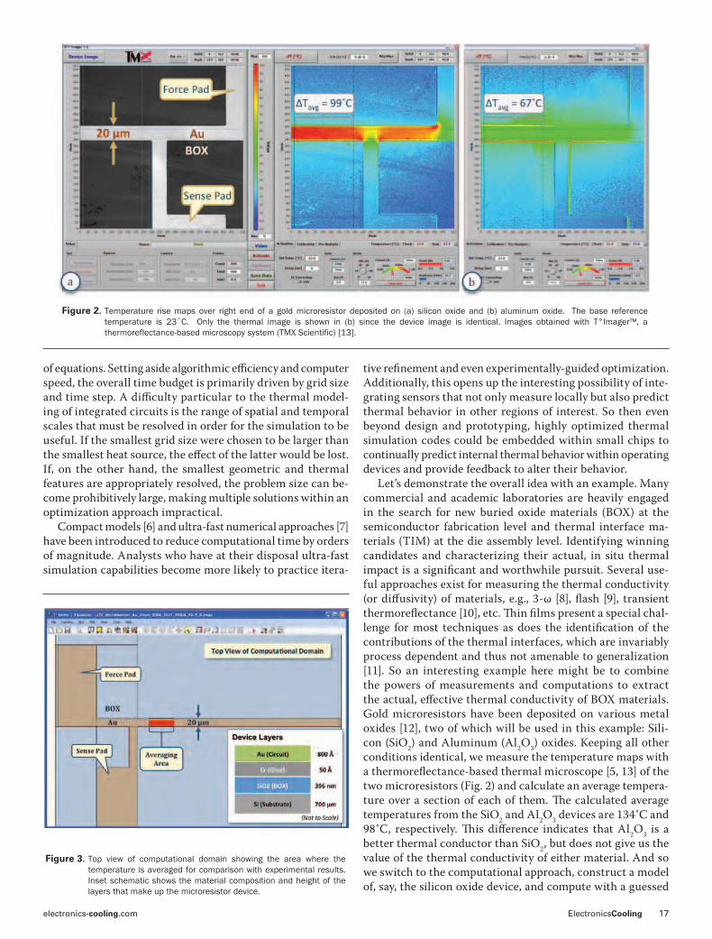
Let’s demonstrate the overall idea with an example. Many commercial and academic laboratories are heavily engaged in the search for new buried oxide materials (BOX) at the semiconductor fabrication level and thermal interface ma-terials (TIM) at the die assembly level. Identifying winning candidates and characterizing their actual, in situ thermal impact is a significant and worthwhile pursuit. Several use-ful approaches exist for measuring the thermal conductivity (or diffusivity) of materials, e.g., 3-ω [8], flash [9], transient thermoreflectance [10], etc. Thin films present a special chal-lenge for most techniques as does the identification of the contributions of the thermal interfaces, which are invariably process dependent and thus not amenable to generalization [11]. So an interesting example here might be to combine the powers of measurements and computations to extract the actual, effective thermal conductivity of BOX materials. Gold microresistors have been deposited on various metal oxides [12], two of which will be used in this example: Sili-con (SiO2) and Aluminum (Al2O3) oxides. Keeping all other conditions identical, we measure the temperature maps with a thermoreflectance-based thermal microscope [5, 13] of the two microresistors (Fig. 2) and calculate an average tempera-ture over a section of each of them. The calculated average temperatures from the SiO2 and Al2O3 devices are 134˚C and 98˚C, respectively. This difference indicates that Al2O3 is a better thermal conductor than SiO2, but does not give us the value of the thermal conductivity of either material. And so we switch to the computational approach, construct a model of, say, the silicon oxide device, and compute with a guessed
Figure 3. Top view of computational domain showing the area where the temperature is averaged for comparison with experimental results. Inset schematic shows the material composition and height of the layers that make up the microresistor device.
Figure 2. Temperature rise maps over right end of a gold microresistor deposited on (a) silicon oxide and (b) aluminum oxide. The base reference temperature is 23˚C. Only the thermal image is shown in (b) since the device image is identical. Images obtained with T°Imager™, a thermoreflectance-based microscopy system (TMX Scientific) [13].

18ElectronicsCooling Winter 2010
initial value of the effective conductivity (or diffusivity) of SiO2 (Fig. 3). It would make sense to start with the published value of 1.4 W/m-K and even assume that our material interfaces are perfect. Simulating the conduction heat transfer problem with an ultra-fast, self-adaptive computational engine [7, 13] and calculating an average value over the corresponding area that we measured gives an average surface temperature of 102˚C. This discrepancy of 32˚C (or 24%) guides us to modify our input value downwardly from 1.4 W/m-K. Repeating the simulation with effective thermal conductivities for the SiO2layer of 1.2, 0.9, and 0.8 W/m-K yields average temperature values of 110˚C (18% lower), 128˚C (5% lower), and 137˚C (2% higher), respectively. A final effective conductivity of 0.83 W/m-K yields the experimentally obtained average tempera-ture of 134˚C. The deduced value for the effective thermal conductivity of thermally grown silicon oxide coincides well with previous measurements obtained with a purely ex-perimental technique [14]. Each of these converged transient computations required just 23 seconds of CPU time on a 3 GHz Pentium 4 desktop computer. Of course, the reader is immediately aware that this approach can be automated and that other important geometric and physical parameters can be included in the optimization process. The purpose of this basic example was simply to step through the optimization process and to demonstrate the power and usefulness of cou-pling experimental and computational approaches.
We must remain open to and work toward breakthroughs in metrology. A groundbreaking non-invasive technology, such as what happened with CT-Scan or MRI for seeing within the human body, could come along to enable us to measure tem-peratures deep within 3D devices. But in the meantime, we need to try to fully leverage what we already have. Extending the life of Moore’s Law is a good enough reason.
RefeRences1. “What’s Happening: 3D Chip Stacking Will Take Moore’s Law Past 2020,
Pose New Challenges,” ElectronicsCooling, Vol. 16, 2010, p. 28.
2. Cale, T.S., Lu, J.Q., and Gutmann, R.J., “Three-Dimensional Integration in Microelectronics: Motivation, Processing, and Thermomechanical Modeling,” Chemical Engineering Communications, Vol. 195, 2008, pp. 847–888.
3. Childs, P.R.N., Greenwood, J.R., and Long, C.A., “Review of Temperature Measurement,” Review of Scientific Instruments, Vol. 71, No. 8, 2000, pp. 2959-2979.
4. Farzaneh, M., Maize, K., Luerßen, D., Summers, J.A., Mayer, P.M., Raad, P.E., Pipe, K.P., Shakouri, A., Hudgings, J.A., and Ram, R., “CCD-Based Thermoreflectance Microscopy: Principles and Applications,” Journal of Physics D: Applied Physics, Vol. 42, 2009, pp. 143001-143021.
5. Raad, P.E., Komarov, P.L., and Burzo, M.G., “An Integrated Experimental and Computational System for the Thermal Characterization of Complex Three-Dimensional Submicron Electronic Devices,” IEEE Transactions on Components and Packaging Technologies, Vol. 30, 2007, pp. 597-603.
6. Lasance, C.J.M., "Ten Years of Boundary-Condition-Independent Compact Thermal Modeling of Electronic Parts: A Review,” Heat Transfer Engineering, Vol. 29, 2008, pp. 149–168.
7. Wilson, J.S. and Raad, P.E., “A Transient Self-Adaptive Technique for Modeling Thermal Problems with Large Variations in Physical Scales,” International Journal of Heat and Mass Transfer, Vol. 47, 2004, pp. 3707-3720.
8. Cahill, D. G., “Thermal Conductivity Measurement from 30 to 750 K: the 3ω Method,” Review of Scientific Instruments, Vol. 61, 1990, pp. 802-809.
9. Parker, W.J., Jenkins, R.J., Butler, C.P., and Abbott, G.L., “Flash Method of Determining Thermal Diffusivity, Heat Capacity, and Thermal Conductivity,” Journal of Applied Physics, Vol. 32, 1961, pp. 1679-1684.
10. Komarov, P.L., and Raad, P.E., “Performance Analysis of the Transient Thermo-Reflectance Method for Measuring the Thermal Conductivity of Single Layer Materials,” International Journal of Heat and Mass Transfer, Vol. 47, 2004, pp. 3233-3244.
11. Lasance, C.J.M., Murray, C., Saums, D., and Rencz, M., “Challenges in Thermal Interface Material Testing,” Proceedings of the 22nd IEEE SEMI-THERM Symposium, Dallas, TX, 2006.
12. Lee, T., Aliev, A., Burzo, M., Komarov, P., Raad, P., and Kim, M., “New SOI Substrate with High Thermal Conductivity for High Performance Mixed-Signal Applications,” 218th Electrochemical Society (ECS) Meeting, Las Vegas, NV, Oct. 2010.
13. T°Imager™ and T°Solver™ are registered trademarks and products of TMX Scientific, Inc.
14. Burzo, M.G., Komarov, P.L., and Raad, P.E., “Thermal Transport Properties of Gold-Covered Thin-Film Silicon Dioxide,” IEEE Transactions on Components and Packaging Technologies, Vol. 26, 2003, pp. 80-88. l
Figure 4. Temperature contours on a horizontal slide on the top surface and a vertical slice through the middle of the microresistor. Computations and images obtained with T°Solver™, an ultra-fast, self-adaptive heat transfer simulation engine (TMX Scientific) [13].
www.electronics-cooling.com
Whatever the needs of a particular application, find a wide choice of manufacturers in the electronics-cooling.com
Buyer’s Guide section.
Just log on to www.electronics-cooling.com, click on Buyer’s Guide, and make your selection.
More on the Web


Have you visited electronics-cooling.com lately?We recently re-launched the site!
Visit www.electronics-cooling.com for the most up-to-date information on Thermal Management:• Industry news• Information sorted by industry and application• New product listings• Buyer’s Guide • Archives of ElectronicsCooling magazines• Industry event and symposium listings• Access to free software trials • On- demand webinars• A chance to follow ElectronicsCooling through our blogs and Twitter (e_cooling)• And much more!

28 ElectronicsCooling Winter 2010
M any of our day-to-day activities, including Internet searches, handheld electronics usage, automated cash withdrawal, and online hotel and airline reservations,
require the use of remote databases and computational in-frastructure comprised of large server farms located at some faraway location from the consumer. Comparable computer facilities also support several critical functions of national security and are indispensible for reliable functioning of our economy. These Information Technology (IT) data centers now consume a large amount of electricity in the U.S. and world-wide. As illustrated in Figure 1, in addition to the issue of the total energy used by IT data centers, the projected usage can be estimated to rise much faster than the other industrial sec-tors [1-3]. The projections were determined by fitting a curve to the available data and extrapolating into the future. Thus, the topic of data center energy efficiency has attracted a large amount of interest from industry, academia, and government regulatory agencies [4, 5].
Cooling has been found to contribute about one third of the energy use of IT data centers and is the focus of this article. Figure 2 displays a schematic of the cooling loop of a typical data center [6]. In such a data center, sub-ambient tempera-ture refrigerated water leaving the chiller plant evaporator is circulated through the Computer Room Air Conditioning (CRAC) units using building chilled water pumps. This water carries heat away from the air-conditioned raised floor room that houses the IT equipment and rejects the heat into the refrigeration chiller evaporator via a heat exchanger. The re-frigeration chiller operates on a vapor compression cycle and
Madhusudan Iyengar is a Senior Engineer at the IBM Poughkeepsie Advanced Thermal Laboratory working on advanced energy-
efficient cooling technologies and concepts for servers and data centers. He received his BE in Mechanical Engineering from the University of Pune, India in 1994, and his
PhD in Mechanical Engineering from the University of Minnesota in 2003. He is a
member of ASME, IEEE, ASHRAE, and IMAPS. He has co-authored over 80 technical papers in journals, conferences and book chapters,
and holds more than 55 issued US patents.
Dr. Roger R. Schmidt, IBM Fellow, National Academy of Engineering Member, IBM
Academy of Technology Member and ASME Fellow, has over 30 years experience in
engineering and engineering management in the thermal design of IBM’s large scale computers. He is IBM’s Chief Engineer on
Data Center Energy Efficiency. He has led development teams in cooling mainframes, client/servers, parallel processors and test equipment utilizing such cooling mediums
as air, water, and refrigerants. He now leads IBM's lab services team on providing
customer support for power and cooling issues in data centers. He has published more than 100 technical papers and has over 100 patents/patent pending in the
area of electronic cooling. He has been an Associate Editor of the Journal of Electronic
Packaging, ASHRAE Research Journal and the ASME Journal of Heat Transfer. He is
past Chair of the ASHRAE TC9.9 committee on Mission Critical Facilities, Technology
Spaces, and Electronic Equipment.
Energy Consumption of InformationTechnology Data Centers
Madhusudan Iyengar and Roger Schmidt IBM, Poughkeepsie, New York
Figure 1. Data [1] and projections [2, 3] for US delivered electricity consumption by sector.

electronics-cooling.com ElectronicsCooling 29
consumes compression work (compressor). The refrigerant loop rejects the heat into a condenser water loop using another chiller heat exchanger (condenser). A condenser pump circu-lates water between the chiller condenser and an air cooled evaporative cooling tower. The air cooled cooling tower uses forced air movement and water evaporation to extract heat from the condenser water loop and transfer it into the ambient environment. Thus, in this “standard” facility cooling design, the primary cooling energy consumption components are: the server fans, the computer room air conditioning unit (CRAC) blowers, the building chilled water (BCW) pumps, the refrig-eration chiller compressors, the condenser water pumps, and the cooling tower blowers.
There are many variations to the plant level cooling infra-structure illustrated in Figure 2. For example, the CRAC could be comprised of a refrigerant loop with an air-cooled roof-top condenser, or the chiller might be eliminated with cooling tower water being routed to a water-to-water economizer heat exchanger, or the outside air could be directly introduced into the data center rooms. The cooling configuration at the server and in its immediate vicinity could also vary significantly. All these and other such “non-standard” configurations are not discussed in this article.
Figure 3 provides a typical breakdown of the energy us-age of a data center using a chilled water loop as depicted in Figure 2. The IT equipment usually consumes about 45-55% of the total electricity, and total cooling energy consumption is roughly 30-40% of the total energy use. As discussed ear-lier, the cooling infrastructure is made up of three elements, the refrigeration chiller plant (including the cooling tower fans and condenser water pumps, in the case of water-cooled condensers), the building chilled water pumps, and the data center floor air-conditioning units (CRACs). About half the cooling energy used is consumed at the refrigeration chiller compressor and about a third is used by the room level air-conditioning units for air movement, making them the two primary contributors to the data center cooling energy use.
Figure 4 depicts the energy flow for a typical data center fa-cility that consists of all the elements that have been discussed above. A detailed description of the thermodynamic model summarized in this paper can be found in the literature [6, 7].
The total electrical pumping power consumed in cooling the data center facility via the various daisy chained loops shown in Figure 4 can be given by [6, 7],
Ptotal = Prack,total +PCRAC +PBCW +Pchiller +PCTW +PCTA (1)where Ptotal, Prack,total, PCRAC, PBCW, Pchiller, PCTW, and PCTA are
the powers consumed by the total facility for cooling, server fans in rack cluster being cooled in the data center room, data center room air-conditioning units, building chilled water pumps, refrigeration chiller plant, cooling tower pumps, and by the cooling tower fans, respectively. Except for the Pchillerterm, all the elements making up the right hand side of eq.(1) can be calculated using the equation below,
P = ∆P x flow / η (2)where P, ∆P, flow, and η are the coolant pumping power
(air or water) at the motor (W), the line pressure drop (N/m2), the coolant volumetric flow rate (m3/s), and the motor electromechanical efficiency, respectively.
To calculate the pressure drop used in eq. (2), one can es-
timate the coolant line pressure drop, ∆P, using,∆P = C2 x flow2 (3)where C represents the coolant pressure loss coefficient
through the rack (server node, rack front and rear covers), the air-conditioning unit (CRAC) and the data center floor associated with a specific CRAC unit, the building chilled water loop piping, the cooling tower water loop piping, or the cooling tower air-side open loop, respectively. Except for the CRAC flow loop pressure loss coefficient terms, all the other coefficients can be calculated or derived using empirical data from building data collection systems or manufacturer’s cata-logues for the various components. The pressure loss arising
Figure 2. Schematic of the data center cooling infrastructure [4].

30 ElectronicsCooling Winter 2010
from flow through the under floor plenum of a raised floor data center and through the perforated tiles is usually an order of magnitude smaller than the pressure loss through the CRAC unit itself. The pressure drop through the CRAC unit is made up primarily from the losses due to the tube and fin coils, the suction side air filters, and several expansion, contraction, and turning instances experienced by the flow [6, 7].
Pchiller is the work done at the refrigeration chiller compres-sor and is calculated using a set of equations that characterize the chiller. While there are several analytical models in the literature which help characterize chiller operation, a version of the Gordon-Ng model [8] was chosen by the authors [6, 7] for its simplicity and the ease with which commonly available plant data can be analyzed to find the model coefficients. The chiller thermodynamic work is a function of the heat load at its evaporator, the temperature of water entering the con-denser, the desired set point temperature of the water leaving the evaporator, as well as several other operating and design parameters including the loading of the chiller with respect to its rated capacity.
While the calculation of the cooling power for the different coolant loops displayed in Figure 4 is relatively straightfor-ward, the thermal analysis is significantly more complex. For example, the heat removed by the cooling tower needs to be equal to the sum of the heat rejected at the refrigeration chiller
condenser and the energy expended by the condenser water pumps. Another example of the thermal coupling necessary to satisfy energy balance is that the heat extracted by the CRAC units needs to be equal to the sum of the heat dissipated by the IT equipment and the CRAC blowers. Detailed models for the calculation of the heat transfer that occurs in various parts of the facility cooling infrastructure depicted in Figure 4 can be found in literature [7].
For the results shown in this article, two cases are consid-ered for which the relevant input conditions are described below. A 350 rack cluster is assumed, with each rack consisting of 42 “pizza box” servers which are each 1U tall (1U = 1.75” or 44.45 mm). Each rack has an estimated maximum power dis-sipation of 16.8 kW and a rack air flow rate of 2160 cubic feet per minute (1.02 m3/s). Assuming two 100 W CPUs for every server, and another 200 W of supporting device heat load, one can assume 400 W/U server load yielding a rack of 16.8 kW for a 42U tall rack. A 2000 ton (1 ton = 3.517 kW) refrigeration chiller is used for cooling this data center.
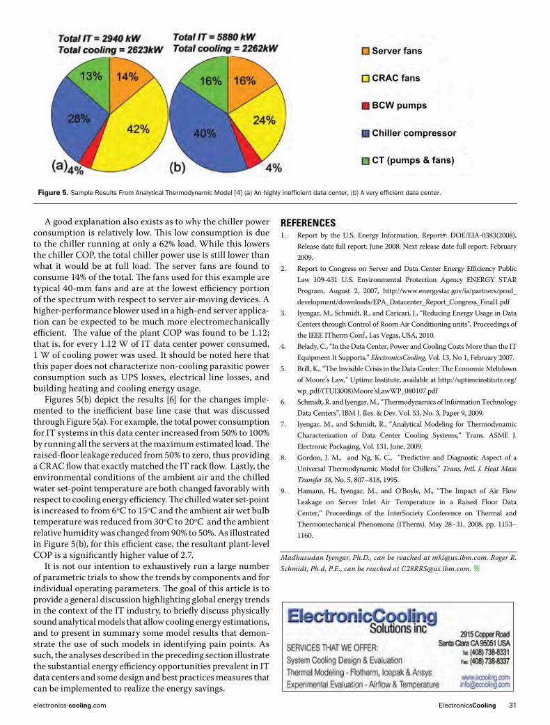
Figure 5(a) shows sample results [6] of thermodynamic analyses using the model [5] that was briefly discussed in the preceding text. This result represents a typically inefficient configuration. For this base line case the chiller supplies 6oC water to the CRACs when the outside air is at 30oC (wet bulb) with a relative humidity of 90%. The servers are assumed to be dissipating only 50% of the initially estimated full load of 16.8 kW, thus, only 8.4 kW. Such configurations are not uncommon. The actual power drawn could be much less than the nameplate information, or the servers might be idle. Thus, although the chiller is rated for 2000 tons (7032 kW), it is being loaded to only 62%. For this case, it is assumed that half the air supplied by the CRAC units is being misdirected to locations other than the cold aisle, that is, a leakage flow of 50% [9]. Thus, the CRAC units are supplying twice as much chilled air flow as is required to satisfy 100% flow through the racks, which is also quite common. A total cooling power of 2.62 MW is consumed for cooling 2.94 MW of server electronics heat load. Counter to what may be expected, the chiller contribution to the energy consumption is not the largest fraction (28%), but the CRAC power consumption is at 42%. The cumulative contribution of the chillers and CRAC is as expected, at 80%. All 101 CRAC units are running at the highest speeds, even though the servers are powered to only 50% of their estimated maximum capacity.
Figure 4. Energy Flow Schematic of a Typical Data Center [6, 7].
Figure 3. Typical breakdown of the data center energy consumption.
electronics-cooling.com ElectronicsCooling 31
A good explanation also exists as to why the chiller power consumption is relatively low. This low consumption is due to the chiller running at only a 62% load. While this lowers the chiller COP, the total chiller power use is still lower than what it would be at full load. The server fans are found to consume 14% of the total. The fans used for this example are typical 40-mm fans and are at the lowest efficiency portion of the spectrum with respect to server air-moving devices. A higher-performance blower used in a high-end server applica-tion can be expected to be much more electromechanically efficient. The value of the plant COP was found to be 1.12; that is, for every 1.12 W of IT data center power consumed, 1 W of cooling power was used. It should be noted here that this paper does not characterize non-cooling parasitic power consumption such as UPS losses, electrical line losses, and building heating and cooling energy usage.
Figures 5(b) depict the results [6] for the changes imple-mented to the inefficient base line case that was discussed through Figure 5(a). For example, the total power consumption for IT systems in this data center increased from 50% to 100% by running all the servers at the maximum estimated load. The raised-floor leakage reduced from 50% to zero, thus providing a CRAC flow that exactly matched the IT rack flow. Lastly, the environmental conditions of the ambient air and the chilled water set-point temperature are both changed favorably with respect to cooling energy efficiency. The chilled water set-point is increased to from 6oC to 15oC and the ambient air wet bulb temperature was reduced from 30oC to 20oC and the ambient relative humidity was changed from 90% to 50%. As illustrated in Figure 5(b), for this efficient case, the resultant plant-level COP is a significantly higher value of 2.7.
It is not our intention to exhaustively run a large number of parametric trials to show the trends by components and for individual operating parameters. The goal of this article is to provide a general discussion highlighting global energy trends in the context of the IT industry, to briefly discuss physically sound analytical models that allow cooling energy estimations, and to present in summary some model results that demon-strate the use of such models in identifying pain points. As such, the analyses described in the preceding section illustrate the substantial energy efficiency opportunities prevalent in IT data centers and some design and best practices measures that can be implemented to realize the energy savings.
REfEREnCEs1. Report by the U.S. Energy Information, Report#: DOE/EIA-0383(2008),
Release date full report: June 2008; Next release date full report: February 2009.
2. Report to Congress on Server and Data Center Energy Efficiency Public Law 109-431 U.S. Environmental Protection Agency ENERGY STAR Program, August 2, 2007, http://www.energystar.gov/ia/partners/prod_development/downloads/EPA_Datacenter_Report_Congress_Final1.pdf
3. Iyengar, M., Schmidt, R., and Caricari, J., “Reducing Energy Usage in Data Centers through Control of Room Air Conditioning units”, Proceedings of the IEEE ITherm Conf., Las Vegas, USA, 2010.
4. Belady, C., “In the Data Center, Power and Cooling Costs More than the IT Equipment It Supports,” ElectronicsCooling, Vol. 13, No 1, February 2007.
5. Brill, K., “The Invisible Crisis in the Data Center: The Economic Meltdown of Moore’s Law,” Uptime Institute, available at http://uptimeinstitute.org/wp_pdf/(TUI3008)Moore’sLawWP_080107.pdf
6. Schmidt, R. and Iyengar, M., “Thermodynamics of Information Technology Data Centers”, IBM J. Res. & Dev. Vol. 53, No. 3, Paper 9, 2009.
7. Iyengar, M., and Schmidt, R., ‘‘Analytical Modeling for Thermodynamic Characterization of Data Center Cooling Systems,’’ Trans. ASME J. Electronic Packaging, Vol. 131, June, 2009.
8. Gordon, J. M., and Ng, K. C., ‘‘Predictive and Diagnostic Aspect of a Universal Thermodynamic Model for Chillers,’’ Trans. Intl. J. Heat Mass Transfer 38, No. 5, 807–818, 1995.
9. Hamann, H., Iyengar, M., and O’Boyle, M., ‘‘The Impact of Air Flow Leakage on Server Inlet Air Temperature in a Raised Floor Data Center,’’ Proceedings of the InterSociety Conference on Thermal and Thermomechanical Phenomona (ITherm), May 28–31, 2008, pp. 1153–1160.
Madhusudan Iyengar, Ph.D., can be reached at [email protected]. Roger R. Schmidt, Ph.d, P.E., can be reached at [email protected]. l
Figure 5. Sample Results From Analytical Thermodynamic Model [4] (a) An highly inefficient data center, (b) A very efficient data center.
Server fans
CRAC fans
BCW pumps
Chiller compressor
CT (pumps & fans)

32 ElectronicsCooling Winter 2010
Index Of AdvertisersAdvanced Cooling Technologies ....................................................................................................................................................11
Alpha Novatech, Inc. ............................................................................................................................................... Inside Back Cover
ebm Papst ......................................................................................................................................................................... Back Cover
Electronic Cooling Solutions Inc. ...................................................................................................................................................31
ITEM Publications ..............................................................................................................................................................................27
Malico Inc. .............................................................................................................................................................................................5
Mentor Graphics ..........................................................................................................................................................................15
SEMI-THERM .........................................................................................................................................................................................19
Summit Thermal System Co., Ltd. ......................................................................................................................................................29
The Bergquist Company .......................................................................................................................................... Inside Front Cover

