winter 17 examination subject title: power …msbte.engg-info.website/sites/default/files/w 17 model...
TRANSCRIPT

MAHARASHTRA STATE BOARD OF TECHNICAL EDUCATION (Autonomous)
(ISO/IEC - 27001 - 2005 Certified)
Page 1
MODEL ANSWER WINTER– 17 EXAMINATION Subject Title: Power Electronics Subject Code: Important Instructions to examiners:
1) The answers should be examined by key words and not as word-to-word as given in the model answer scheme. 2) The model answer and the answer written by candidate may vary but the examiner may try to assess the
understanding level of the candidate. 3) The language errors such as grammatical, spelling errors should not be given more Importance (Not applicable for
subject English and Communication Skills. 4) While assessing figures, examiner may give credit for principal components indicated in the figure. The figures
drawn by candidate and model answer may vary. The examiner may give credit for any equivalent figure drawn. 5) Credits may be given step wise for numerical problems. In some cases, the assumed constant values may vary and
there may be some difference in the candidate’s answers and model answer.
6) In case of some questions credit may be given by judgement on part of examiner of relevant answer based on candidate’s understanding.
7) For programming language papers, credit may be given to any other program based on equivalent concept.
Q. No. Sub
Q.N.
Answer Marking
Scheme
Q.1 (A) Attempt any SIX of the following : 12-Total
Marks
a) Draw the symbols of (i) SCR (ii) DIAC 2M
Ans:
1M each
b) State advantages of power transistor (any two) 2M
Ans: 1) It is very easy to turn ON and turn OFF the power transistor.
2) It can carry large currents in ON state and block very high voltage in OFF state.
3) It can be operated at switching frequencies in range of 10 to 15 kHz.
4) ON state voltage drops across power transistor is low.
1M each
c) Define holding and latching current. 2M
17444

MAHARASHTRA STATE BOARD OF TECHNICAL EDUCATION (Autonomous)
(ISO/IEC - 27001 - 2005 Certified)
Page 2
Ans: Holding current(IH): Holding current may be defined as the minimum value of
anode to cathode current below which the SCR stops conducting and returns to its
OFF- state.
Latching current(IL): latching current may be defined as the minimum ON – state
anode to cathode current required to keep the SCR in the ON- state after the
triggering pulse has been removed.
I M each
d) Define chopper. State its types. 2M
Ans: Chopper is a static device (switch) used to obtain variable DC from a source of
fixed DC.
Types of chopper:
1) Step-up chopper
2) Step-down chopper
3) Step up/down chopper
Definition-
1M
Types-1M
e) List different turn-on methods of SCR. 2M
Ans: Turn – ON Methods of SCR:
1) Forward voltage triggering
2) Thermal triggering
3) Illumination triggering
4) dv/dt triggering
5) Gate triggering
a) DC voltage triggering
b) AC voltage triggering
c) Pulse triggering
2M for
correct
answer
f) State the applications of inverter. 2M
Ans: Applications of inverter- 1) Variable speed a c motor drivers
2) Induction heating
3) Aircraft power supplies
4) Uninterrupted power supplies (UPS)
5) High voltage d c transmission lines
6) Battery vehicles drives
7) Regulated voltage and frequency power supplies
Any four to
be given
2M.
g) State the use of freewheeling diode in controlled rectifiers. 2M
Ans: 1) To prevent reversal of load voltage
2) To prevent transfer of reactive power from load to supply and hence to improve
power factor of the circuit.
1M each
h) Draw the circuit diagram of fan speed regulator using TRIAC. 2M
Ans: Circuit diagram-

MAHARASHTRA STATE BOARD OF TECHNICAL EDUCATION (Autonomous)
(ISO/IEC - 27001 - 2005 Certified)
Page 3
2M
(B) Attempt any TWO : 8-Total
Marks
8 M
a) Compare controlled and uncontrolled rectifiers. (any four points) 4M
Ans:
Parameter Controlled Rectifier Uncontrolled Rectifier
Device used SCR and Diodes Only Diodes.
Control of Load
Voltage
Load voltage can be
controlled. Load voltage cannot be
controlled.
Direction of Power
Flow
Source to load and sometimes
load to source Source to load only.
Free Wheeling
diode
Required for inductive load Not necessary
Triggering circuit Required. Not required
Applications DC motor controller, Battery
charger. Power supply
1M each for
any four.
b) Draw the circuit diagram and waveforms of step up chopper using MOSFET. 4M
Ans: Circuit diagram:
2M

MAHARASHTRA STATE BOARD OF TECHNICAL EDUCATION (Autonomous)
(ISO/IEC - 27001 - 2005 Certified)
Page 4
Waveforms:
2M
c) Draw the circuit diagram of light dimmer using DIAC and TRIAC and
sketch the input-output waveforms.
4M

MAHARASHTRA STATE BOARD OF TECHNICAL EDUCATION (Autonomous)
(ISO/IEC - 27001 - 2005 Certified)
Page 5
Ans: Circuit Diagram:
Input-output Waveforms:
2M
2M
.
Q 2 Attempt any FOUR : 16-Total
Marks
a) Draw the circuit diagram input-output waveforms and explain the working of
single phase half wave controlled rectifier with R load.
4M
Ans: Circuit Diagram:
1M

MAHARASHTRA STATE BOARD OF TECHNICAL EDUCATION (Autonomous)
(ISO/IEC - 27001 - 2005 Certified)
Page 6
Working:
During the positive half cycle of input voltage, the thyristor T is triggered at an
angle of ωt = α. Now as the thyristor is ON, the load gets directly connected to the
supply. During the negative half cycle, thyristor is reverse biased and is turned OFF.
So the load gets voltage only during positive half cycle. The average value of the
output voltage may be varied by varying the firing angle “α”. As the load is resistive
the current waveform will be identical to that of voltage waveform.
Waveforms:
1M
2M
b) Draw and explain the circuit diagram of series inverter with waveforms. 4M
Ans:

MAHARASHTRA STATE BOARD OF TECHNICAL EDUCATION (Autonomous)
(ISO/IEC - 27001 - 2005 Certified)
Page 7
Circuit Diagram:
Description:
Fig. below shows the circuit of a series inverter. The commutating elements L and C
are in series with the load forming an R-L-C resonating circuit. The value of L&C
are chosen such that, they form an under-damped circuit. This is necessary to
produce the required oscillations. This condition is fulfilled by selecting L & C such
that,
. Cycling of output is achieved by alternately switching ON the
thyristors T1 & T2. A time delay must be maintained between the point when one
SCR is turned OFF and the other is turned ON to avoid a short circuit of the input
source. This type of inverter produces an approximately sinusoidal waveform at a
high output frequency.
2M
1M

MAHARASHTRA STATE BOARD OF TECHNICAL EDUCATION (Autonomous)
(ISO/IEC - 27001 - 2005 Certified)
Page 8
Waveforms:
1M
c) Draw the circuit diagram of emergency lighting system using SCR and
describe its working.
4M
Ans: Circuit diagram:
Working:
Fig. above shows a single source emergency lighting system. Voltage across C1
affects the ON/OFF control of the SCR. When the supply is ON, bulb is connected
to it and will remain ON. Now the battery is charged to a voltage slightly lesser than
2M
2M

MAHARASHTRA STATE BOARD OF TECHNICAL EDUCATION (Autonomous)
(ISO/IEC - 27001 - 2005 Certified)
Page 9
the supply voltage. This will make T1 to reverse bias and is OFF. When supply
fails, capacitor C1 discharges through D3–R3-R4-R1, until the anode becomes
sufficient positive than cathode. At the same time the junctionR1 & R4 becomes
positive and provide sufficient gate to cathode voltage to trigger SCR. As the SCR
is ON the battery gets connected across the bulb making it ON. When the power
returns to normal, as the cathode of T1 becomes more positive w. r to anode it
reverse biases and get commutated disconnecting the battery.
d) Draw and explain the VI characteristics of DIAC 4M
Ans: Description:
The figure below shows the V-I characteristics of DIAC which indicates the current
flow through the DIAC with respect to the voltage across it. As long as the voltage
across the DIAC is within its break-over limits that is from –VBO to +VBO, the
resistance offered by the DIAC is very high and only a small leakage current flows
through the device ( portion OA & OA') as shown in figure. Under these conditions
DIAC operates as an open switch. The voltages +VBO and –VBO are the
breakdown voltages which are generally in the range of 30 to 50 volts.
Once the positive or negative applied voltage is more than the respective breakdown
voltages DIAC start conducting. During the positive half cycle, at point A in the
figure the DIAC begins to conduct and the voltage drop across the device becomes a
few volts. The portion AB represents the conduction of DIAC. Conduction
continuous until the device current falls below its holding current level. The holding
current and break-over voltage values are identical for reverse and forward region of
operation. The first and third quadrant characteristics represent the forward and
reverse bias conditions of the DIAC.
V-I characteristics-
2M
2M

MAHARASHTRA STATE BOARD OF TECHNICAL EDUCATION (Autonomous)
(ISO/IEC - 27001 - 2005 Certified)
Page 10
e) Explain SCR triggering using UJT with neat circuit diagram 4M
Ans: Circuit diagram:
Description:
Fig. shows the basic circuit of SCR triggering using UJT. When the switch SW is
closed at t = 0, capacitor voltage Vc = 0 and the UJT is in the OFF state. Now the
capacitor starts charging and at Vc = Vp UJT turns ON. The UJT current IE
supplied by the capacitor flows through RB1 & R1, discharging the capacitor. When
Vc falls below the valley voltage Vv of the UJT, it turns OFF. This causes
discharging of the capacitor to stop and starts charging again. This cycle continues
till the switch SW is closed creating a train of pulses at B1 and B2. At B1 a train
positive pulses occur during the discharging of capacitor through UJT emitter. The
first pulse occurs at “T” seconds after the switch is closed causing a sufficient gate
current and the SCR turns ON. Once the SCR is ON subsequent pulses at its gate
have no effect. The circuit may cause premature triggering of SCR if the voltage at
B1 is sufficient with UJT OFF. The requirement to avoid this is by following the
below condition.
VB1(OFF) ( Ig. Rg + Vg)
2M
2M
f) Compare step up and step down chopper. (any four points) 4M
Ans:
Parameter Step up chopper Step down chopper
Position of
chopper switch
In parallel with load In series with load
Output voltage More than input voltage Less than input
voltage
Expression of Vdc = Vs/(1-D) Volts Vdc = D.Vs Volts
1M each
MAHARASHTRA STATE BOARD OF TECHNICAL EDUCATION (Autonomous)
(ISO/IEC - 27001 - 2005 Certified)
Page 11
output voltage Where, D= Duty Cycle
Vs= Input voltage
Where,
D= Duty Cycle
Vs= Input voltage
Application Battery charging, voltage
booster
Motor speed control
Q. 3 Attempt any FOUR : 16-Total
Marks
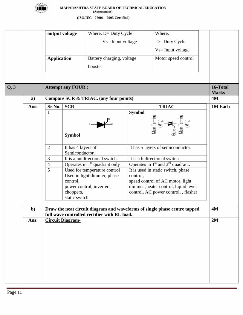
a) Compare SCR & TRIAC. (any four points) 4M
Ans: Sr.No. SCR TRIAC
1
Symbol
Symbol
2 It has 4 layers of
Semiconductor.
It has 5 layers of semiconductor.
3 It is a unidirectional switch. It is a bidirectional switch
4 Operates in 1st quadrant only Operates in 1
st and 3
rd quadrant.
5 Used for temperature control
Used in light dimmer, phase
control,
power control, inverters,
choppers,
static switch
It is used in static switch, phase
control,
speed control of AC motor, light
dimmer ,heater control, liquid level
control, AC power control, , flasher
1M Each
b) Draw the neat circuit diagram and waveforms of single phase centre tapped
full wave controlled rectifier with RL load.
4M
Ans: Circuit Diagram-
2M

MAHARASHTRA STATE BOARD OF TECHNICAL EDUCATION (Autonomous)
(ISO/IEC - 27001 - 2005 Certified)
Page 12
Waveform-
2M
c) Draw and explain the VI characteristics of power transistor. 4M
Ans:

MAHARASHTRA STATE BOARD OF TECHNICAL EDUCATION (Autonomous)
(ISO/IEC - 27001 - 2005 Certified)
Page 13
There are four regions Cutoff region, Active region, quasi saturation and hard
saturation. The cutoff region is the area where base current is almost zero. Hence no
collector current flows and transistor is off.
In the quasi saturation and hard saturation, the base drive is applied and transistor is
said to be on. Hence collector current flows depending upon the load.
The power BJT is never operated in the active region (i.e. as an amplifier) it is
always operated between cutoff and saturation .
The primary breakdown shown takes place because of avalanche breakdown of
collector base junction. Large power dissipation normally leads to primary
breakdown.
The second breakdown shown is due to localized thermal runaway.
2M
2M
d) Draw and explain the VI characteristics of UJT. 4M
Ans: V-I characteristic of UJT. There are two important points on the characteristic curve
namely the peak-point and the valley- point. These points divide the curve into three
important regions i.e , cut off region , negative resistance region and saturation
region.
Diagram-
2M

MAHARASHTRA STATE BOARD OF TECHNICAL EDUCATION (Autonomous)
(ISO/IEC - 27001 - 2005 Certified)
Page 14
1) Cut-off region: The region, to the left peak-point, is called cut-off region. In the
region, the emitter voltage is below the peak-point voltage (Vp) and the emitter
current is approximately zero. The UJT is in its OFF position in this region.
2) Negative resistance region: The region, between the peak –point and the valley-
point called negative – resistance region. In this region, the emitter voltage
decreases from Vp to Vv and the emitter current increases from Ip to Iv. The
increase in emitter current is due to the decrease in resistance rb1. It is because of
this fact that this region is called negative-resistance region. It is the most important
region from the application point of view.
3) Saturation region: the region, beyond the valley point, is called saturation
region. In this region, the device is in its ON position. The emitter voltage (Ve)
remains almost constant with the increasing emitter current.
2M
e) Draw the circuit diagram of single phase fully controlled bridge rectifier with
R load. Draw the waveforms of input and output voltage.
4M
Ans:
2M
2M
f) Describe the need of polyphase rectifier. 4M
Ans: Polyphase Rectifier: Polyphase rectifier has 3 or more phases at input. A rectifier
which utilizes two or more diodes (usually three), each of which operates during an
equal fraction of an alternating current cycle to achieve an output current which
varies less than that in an ordinary half-wave or full wave rectifier. Ripple factor
decreases rapidly with an increase in the number of phase. Poly phase rectifier gives
smooth direct current. Low harmonics in the input supply current .Number of phases
are more due to that average output can be more & hence output power is also more.
High ripple frequency therefore small filters can be used.
4M
Q. 4 A) Attempt any FOUR : 16-Total
Marks

MAHARASHTRA STATE BOARD OF TECHNICAL EDUCATION (Autonomous)
(ISO/IEC - 27001 - 2005 Certified)
Page 15
a) Draw the circuit diagram and waveforms of step down chopper and explain it. 4M
Ans: Diagram:
Working:
When the switch (Power MOSFET) is closed, the supply voltage Vs appears across
the load and when it is open the load is disconnected from the supply. Thus the
average DC output voltage is controlled by controlling the switching on period ton
and switching off period t off . Equation of the output voltage is, Vo = Vdc. α,
where α is the duty cycle.
Waveform: -
1M
2M
1M
b) Draw and explain the VI characteristics of SCR. 4M
Ans: Diagram-
2M

MAHARASHTRA STATE BOARD OF TECHNICAL EDUCATION (Autonomous)
(ISO/IEC - 27001 - 2005 Certified)
Page 16
Explanation-
Forward Blocking mode: When anode is at a higher potential than cathode, thyristor is said to be forward
biased, It is seen from the figure that when the gate circuit is open J1 and J3 are
forward biased and junction J2 is reverse bias.
In this mode a small current, called forward leakage current flows from anode to
cathode.
Forward Conduction mode:
When anode to cathode forward voltage is increased with gate circuit open, reverse
biased junction J2 will have an avalanche breakdown at a voltage called forward
breakover voltage VBO .
After this breakdown, thyristor gets turned ON.
Reverse Blocking mode:
When cathode is made high potential with respect to anode with gate open, then the
SCR is said to be reverse biased.
J1 and J3 are reverse biased and J2 is forward biased.
A small current flows through the SCR this is called as reverse leakage current.
This is reverse blocking mode, called the OFF state of the SCR.
If the reverse voltage increased, then at reverse breakdown voltage VBR, an
avalanche breakdown occurs at J1 and J3 and the reverse current increases rapidly
2M
c) Describe the working of DC flasher circuit using SCR with neat diagram. 4M
Ans: Diagram- 2M
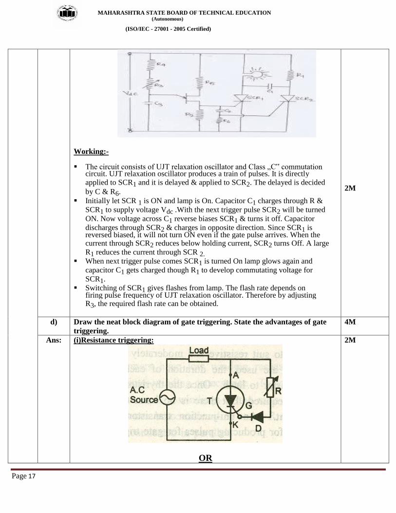
MAHARASHTRA STATE BOARD OF TECHNICAL EDUCATION (Autonomous)
(ISO/IEC - 27001 - 2005 Certified)
Page 17
Working:- The circuit consists of UJT relaxation oscillator and Class „C‟ commutation
circuit. UJT relaxation oscillator produces a train of pulses. It is directly applied to SCR1 and it is delayed & applied to SCR2. The delayed is decided
by C & R6. Initially let SCR 1 is ON and lamp is On. Capacitor C1 charges through R &
SCR1 to supply voltage Vdc .With the next trigger pulse SCR2 will be turned
ON. Now voltage across C1 reverse biases SCR1 & turns it off. Capacitor
discharges through SCR2 & charges in opposite direction. Since SCR1 is reversed biased, it will not turn ON even if the gate pulse arrives. When the current through SCR2 reduces below holding current, SCR2 turns Off. A large
R1 reduces the current through SCR 2.
When next trigger pulse comes SCR1 is turned On lamp glows again and
capacitor C1 gets charged though R1 to develop commutating voltage for
SCR1.
Switching of SCR1 gives flashes from lamp. The flash rate depends on firing pulse frequency of UJT relaxation oscillator. Therefore by adjusting R3, the required flash rate can be obtained.
2M
d) Draw the neat block diagram of gate triggering. State the advantages of gate
triggering.
4M
Ans: (i)Resistance triggering:
OR
2M

MAHARASHTRA STATE BOARD OF TECHNICAL EDUCATION (Autonomous)
(ISO/IEC - 27001 - 2005 Certified)
Page 18
(ii) RC Triggering
OR
Advantages-
Positive gate voltage or gate current
Maximum Permissible gate power dissipation PGM
There are maximum and minimum limits for gate voltage and gate current to
prevent the permanent destruction of junction J3 and to provide the realizable
triggering.
The gate signal can be ac or dc or a sequence of high frequency pulses.
2M
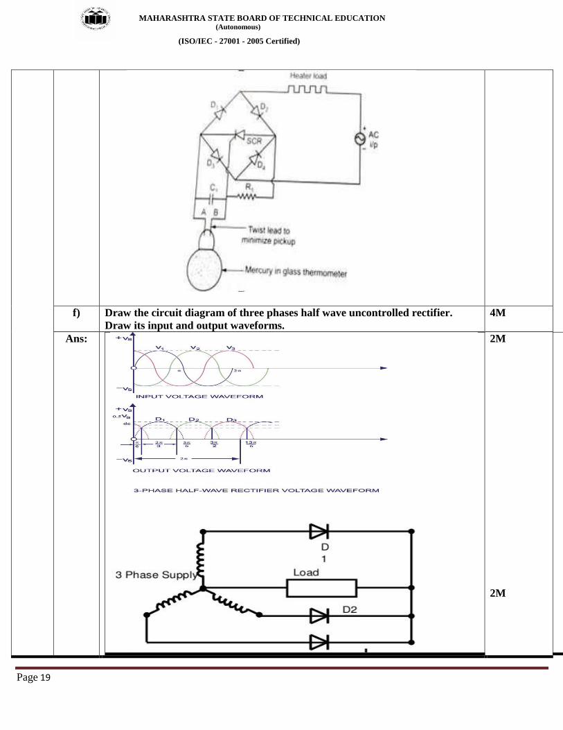
e) Draw the circuit diagram of temperature controller using SCR with neat
circuit diagram.
4M
Ans: 4M
MAHARASHTRA STATE BOARD OF TECHNICAL EDUCATION (Autonomous)
(ISO/IEC - 27001 - 2005 Certified)
Page 19
f) Draw the circuit diagram of three phases half wave uncontrolled rectifier.
Draw its input and output waveforms.
4M
Ans:
2M
2M
2M
2M

MAHARASHTRA STATE BOARD OF TECHNICAL EDUCATION (Autonomous)
(ISO/IEC - 27001 - 2005 Certified)
Page 20
Q.5 Attempt any FOUR : 16-Total
Marks
a) Draw and explain the battery charger using SCR. 4M
Ans:
Explanation :
Automatic battery charging circuit using SCR is shown in figure
A 12 V discharged battery is connected in the circuit.
The single-phase 230 V supply is stepped down to (15-0-15) V by a centre-tapped
transformer. Diodes D1 and D2 form full-wave rectifier. Due to this, the pulsating
d.c. supply appears across the terminals P and Q.
When switch S1 is closed, the pulsating DC voltage appears across terminals P & Q
When SCR1 is OFF, its cathode is held at the potential of discharged battery.
During each positive half-cycle when the potential of point O rises to sufficient level
so as to forward bias diode D3 & gate – cathode junction of SCR1 , the gate pulse is
provided to SCR1 and it is turned ON.
When SCR1 is turned ON, the charging current flows through the battery.
Thus, during each positive half-cycle of pulsating d.c. supply, voltage across P-Q,
SCR1 is triggered and charging current is passed till the end of that half-cycle.
Due to the zener diode Dz, the maximum voltage of point O is held at 12 V.
Due to the charging process, the battery voltage rises and finally attains full value of
12 V.
Thus, when the battery is fully charged, the cathode of SCR1 is held at 12 V.
Therefore diode D3 anode voltage & cathode voltage becomes 12 V & hence D3
and gate-cathode junction of SCR1 cannot be forward biased, since the potential of
point O can reach upto 12 V. Hence, no gate-current is supplied and SCR1 is not
triggered.
In this way, after charging further charging is automatically stopped.
2M
2M
b) Draw the construction of GTO & explain the working principle. 4M
Ans: Diagram: - 2M

MAHARASHTRA STATE BOARD OF TECHNICAL EDUCATION (Autonomous)
(ISO/IEC - 27001 - 2005 Certified)
Page 21
Working :
The turn ON operation of GTO is similar to a conventional thyristor. When
the anode terminal is made positive with respect to cathode by applying a
positive gate current, the hole current injection from gate forward bias the
cathode p-base junction.
This results in the emission of electrons from the cathode towards the anode
terminal. This induces the hole injection from the anode terminal into the
base region. This injection of holes and electrons continuous till the GTO
comes into the conduction state.
To turn OFF a conducting GTO, a reverse bias is applied at the gate by
making the gate negative with respect to cathode. A part of the holes from
the P base layer is extracted through the gate which suppresses the injection
of electrons from the cathode.
In response to this, more hole current is extracted through the gate results
more suppression of electrons from the cathode. Eventually, the voltage drop
across the p base junction causes to reverse bias the gate cathode junction
and hence the GTO is turned OFF.
2M
c) Describe the operation of pulse transformer used in triggering circuits. 4M
Ans:
Pulse transformers are often used to couple a trigger pulse generator to a thyristor in
2M

MAHARASHTRA STATE BOARD OF TECHNICAL EDUCATION (Autonomous)
(ISO/IEC - 27001 - 2005 Certified)
Page 22
order to obtain electrical isolation between the two circuits. The transformers
commonly used for thyristor control are either 1:1 two winding or 1:1:1 three
winding types. Figure shows a complete output circuit to fire a thyristor correctly.
The series resistor R either reduces the SCR holding current or balances gate current
in a three winding transformer connected to two SCRs. The series diode D prevents
reverse gate current in the case of ringing or reversal of the pulse transformer output
voltage. The diodes also reduce holding current of the SCR. In some cases where
high noise levels are present it may be necessary to load the secondary of the
transformer with a resistor to prevent false triggering.
2M
d) Explain RC triggering circuit with neat circuit diagram & waveforms. 4M
Ans: Circuit diagram-
Description:
The triggering angle control limitation of the resistance triggering circuit (R
triggering) can be overcome by the -resistance-capacitance (RC) triggering circuit.
The figure shows the RC-half wave trigger circuit. The conduction period can be
controlled over the full 180° range. By varying the value of Rv, the trigger can be
controlled from 0 to П
1. During the positive half cycle, the capacitor C charges to the trigger voltage of the
thyristor in a time determined by the RC time constant and the applied anode
voltage.
2. During the negative half cycle, the capacitor charges to the peak supply voltage at
t = (-П/2). After this period, the supply voltage decreases and reaches zero at t =
0.During this period the capacitor voltage becomes positive during the positive half
cycle of the ac input, the capacitor begins to charge through the variable resistance
Rv, in the opposite direction and as soon as it charges to a positive voltage equal to
the gate trigger voltage, the thyristor turns ON.
Here the diode D1 is used to prevent the negative voltage between the gate and the
cathode through the diode D2 during the negative half-cycle
Waveform:-
1 ½ M
1 ½ M

MAHARASHTRA STATE BOARD OF TECHNICAL EDUCATION (Autonomous)
(ISO/IEC - 27001 - 2005 Certified)
Page 23
1M
e) Draw the symbol & vertical structure of power transistor and explain. 4M
Ans: Symbol-
Explanation-
Fig. shows the doping level in each layer. The thickness of the different layer will
have a significant effect on the characteristics of the device.
1) The emitter layer is heavily doped the base is moderately doped. The n region is
Symbol-
1M,
vertical
structure-
1.5 M
Collector pnp BJT Emitter
Base Collector npn BJT Emitter
Base
Emitter Base
n + 10 19 cm -3
p 10 16 cm -3
n – 10 14 cm -3
n + 10 19 cm -3
Collector
m 250
50-200 m
m 10
5-20 m
Collector drift ( region)
Base Thickness

MAHARASHTRA STATE BOARD OF TECHNICAL EDUCATION (Autonomous)
(ISO/IEC - 27001 - 2005 Certified)
Page 24
known as the collector drift region and it is lightly doped. The n region is known as
the collector drift region and it is lightly doped then n+ that terminates. The drift
region has doping level similar to that of emitter. This n+ region serves as collector
contact.
2) Due to the doping level the n drift layer will increase the voltage blocking
capacity of the transistor. The width of this layer decides the breakdown voltage of
power transistor.
3) The current gain β of a transistor depends on the base thickness. As the base
thickness reduces the gain increases but the breakdown voltage of transistor will
decrease. In power transistor high breakdown voltage is more important than high
current gain. Therefore the base thickness much larger than that in the logic level
transistor.
1.5M
f) Define firing angle and conduction angle. What is the effect of firing angle on
average output voltage?
4M
Ans: Firing angle (α) - The angle of sine wave at which SCR is turned ON is called as
firing angle . It is denoted by α & it varies from 0 to 1800
Conduction angle (β) – The angle at which SCR remains in conduction state is
known as its conduction angle. . It is denoted by β
β =π-α
Note: waveform optional
Effect of changing α : Output voltage of controlled rectifier is inversely
proportional to firing angle . As α is 0° then output voltage of rectifier is maximum
and when α is 180° then output voltage of rectifier is minimum.
As firing angle α increases output DC voltage of rectifier decreases.
Each
definition
1M,Effect
2M
Q.6 Attempt any FOUR : 16-Total
Marks
a) Draw and explain the C of electronic timer using SCR. 4M
Ans: Diagram-
2M

MAHARASHTRA STATE BOARD OF TECHNICAL EDUCATION (Autonomous)
(ISO/IEC - 27001 - 2005 Certified)
Page 25
Explanation-
Electronic timer are actually a time delay relay , which provide a delayed switching
action between the time an event is initiated and the time the event is actually
performed.
Fig. shows the basic electronic timer circuit using UJT & thyristor to switch a
control relay ON and OFF.
R1 & C1 = RC network
When the switch s is closed, the capacitor C1 begins to charge until the current at the
emitter of the UJT is sufficient to switch the UJT on. This produces a trigger pulse to
the thyristor T1 and latches the control relay.[i.e relay is energized]
By varying the value of the resistor R1 and the Capacitor C1 , the time delay of the
relay can be delayed or advanced .
This is the simplest type of electronic timer that uses a charging rate characteristics
of a capacitor whose charging / discharging depends on the size of the capacitor and
resistor.
2M
b) Draw the circuit diagram of three phase controlled half wave rectifier with R
load. Draw its input and output waveforms.
4M
Ans: Circuit diagram-
2M

MAHARASHTRA STATE BOARD OF TECHNICAL EDUCATION (Autonomous)
(ISO/IEC - 27001 - 2005 Certified)
Page 26
Waveform-
OR
Output waveform-
2M
c) Draw & explain the class C commutation with neat circuit diagram and
waveforms.
4M
Ans: Circuit diagram-
2M

MAHARASHTRA STATE BOARD OF TECHNICAL EDUCATION (Autonomous)
(ISO/IEC - 27001 - 2005 Certified)
Page 27
Description:
Here complementary thysistor T2 is connected in parallel with the main thysistor.
Initially both the thysistors are OFF when a trigerring pulse is applied to the gate
T1,the transistor T1 is trigerred .therefore current starts flowing through the load as
well as R2 & C . Capacitor C will get charged by the supply voltage Edc as shown in
Fig,
When a troerring pulse is applied to the gate of T2 , T2 will be turned on. As soon as
T2 is ON.the negative polarity of capacitor C is applied to the anode of T1 & positive
to the cathode. This causes reverse bias voltage across the main thyristor T1 &
immediately turns it off.
1M
1M
d) Draw and explain the two transistor analogy of SCR. 4M
Ans: Diagram:-
2M

MAHARASHTRA STATE BOARD OF TECHNICAL EDUCATION (Autonomous)
(ISO/IEC - 27001 - 2005 Certified)
Page 28
Working:-
The operation of an SCR can be explained in a very simple way by considering it in
terms of two transistors.
The SCR can be considered as an npn & pnp transistor, where the collector of one
transistor is attached to the base of the other & vice versa. This gives net gain of
loop circuit as 1x2 are where 1x2 are current gains of two transistors
respectively.
The collector current of transistor T1 becomes the base of transistor T2 & vice versa
&
Ic1= Ib2
Ib1=Ic2
When the gate current is zero or the gate terminal is open , the only current in
circulation is the leakage current , which is very small. Under these conditions P-N-
P-N device is said to be in its forward blocking or high impedance off state .
As soon as a small amount of gate current is given of transistor T2 by applying
forward bias to its base emitter junction it generates the collector current as 2 times
the base current. This collector current of T2 is fed as input base current toT1 which
is futher multiplied by 1 times the base current i.e collector current of transistor T2
In this way both transistors feedback each other and the collector current of each
goes multiplying . This process is very quick & soon both the transistors drive each
other into saturation. Now the device is said to be in on-state from the OFF-state.
This characteristic of the device is known as its regenerative action.
2M
e) Describe the construction of IGBT. 4M
Ans: Constructional diagram- 2M

MAHARASHTRA STATE BOARD OF TECHNICAL EDUCATION (Autonomous)
(ISO/IEC - 27001 - 2005 Certified)
Page 29
Explanation-
Basic structure of IGBT:-
Vertical cross section of n channel IGBT is Shown in the figure.
Vertically oriented structure is used to maximize the area available for the
current flow. This will reduce the resistance offered to the current flow and
hence the on-state power loss taking place in the device.
These IGBT uses highly inter digitated gate source structure in the order to
reduce the possibility of source / emitter current crowding.
The vertical cross- section of IGBTis shown in the figure.
IGBT have 4 alternate p-n-p-n layers with three terminals, ex. Emitter, collector
& gate or source, drain & gate.
A heavily doped p+ substrate ( injection layer) has a lightly doped n-type drift
region grown on to it by the epitaxial process.
Then the p type emitter is diffused with 2 subsequent n-type layers over doping
n-type layers over doping windows .
Two SIO2 layers are then deposited & deposition of the metal or polysilicon
layer on them forms an interconnected gate
From this, figure , it is clear that the emitter to collector path is basically a p-n-p
bipolar structure, therefore , these performance of an IGBT is closer to that of a
BJT rather than a MOSFET.
2M
f) Define commutation. List various types of commutation. 4M
Ans: Definition- Commutation: The process to turn off conducting SCR is called commutation.
Types of commutation:- ( natural commutation and forced commutation)
i) Class A- Self commutation by resonating the load
ii) Class B- Self commutation by an LC circuit
iii) Class C- Complementary commutation
1M
3M

MAHARASHTRA STATE BOARD OF TECHNICAL EDUCATION (Autonomous)
(ISO/IEC - 27001 - 2005 Certified)
Page 30
iv) Class D- Impulse or auxiliary commutation
v) Class E- External pulse commutation
vi) Class F- AC line commutation