wideband and fast thz spectrometer using dual-frequency
TRANSCRIPT

Wideband and Fast THz Spectrometer Using
Dual-Frequency-Comb on CMOS
by
Cheng Wang
Submitted to the Department of Electrical Engineering and ComputerScience
in partial fulfillment of the requirements for the degree of
Master of Science in Electrical Engineering and Computer Science
at the
MASSACHUSETTS INSTITUTE OF TECHNOLOGY
June 2018
Massachusetts Institute of Technology 2018. All rights reserved.
Autor....Signature redactedA uthor ......... ..................
Department of Electrical Engineering and Computer ScienceMay 22, 2018
Certified by.......................Signature redactedRuonan Han
Assistant Professor of Electrical Engineering and Computer ScienceThesis Supervisor
Accepted by.....................Signature redactedtesWeW. Kolodziejski
Professor of Electrical Engineering and Computer ScienceChair, Department Committee on Graduate Students
MASSACHUSETTS INSTITUTE (lOF TECHNOLOGY Ij
JUN 18 2018
LIBRARIES

2
Wideband and Fast THz Spectrometer Using
Dual-Frequency-Comb on CMOS
by
Cheng Wang
Submitted to the Department of Electrical Engineering and Computer Scienceon May 22, 2018, in partial fulfillment of the
requirements for the degree ofMaster of Science in Electrical Engineering and Computer Science
Abstract
Millimeter-wave/terahertz rotational spectroscopy of polar gaseous molecules pro-vides a powerful tool for complicated gas mixture analysis. Here, a 220-to-320 GHzdual-frequency-comb spectrometer in 65-nm bulk CMOS is presented, along with asystematic analysis on fundamental issues of rotational spectrometer, including theimpacts of various noise mechanisms, gas cell, molecular properties, detection sensitiv-ity, etc. The spectrometer utilizes two counter-propagating frequency-comb signals toseamlessly scan the broadband spectrum. The comb signal, with 10 equally-spacedfrequency tones, is generated and detected by a chain of inter-locked transceiverson chip. Each transceiver is based on a multi-functional electromagnetic structure,which serves as frequency doubler, sub-harmonic mixer and on-chip radiator simul-taneously. In particular, theory and design methodology of a dual transmission linefeedback scheme are presented, which maximizes the transistor gain near its cut-offfrequency fmax. The dual-frequency-comb scheme does not only improve the scan-ning speed by 20 x, but also reduces the overall energy consumption to 90 mJ/pointwith 1 Hz bandwidth (or 0.5 s integration time). With its channelized 100-GHzscanning range and sub-kHz specificity, wide range of molecules can be detected.In the measurements, state-of-the-art total radiated power of 5.2 mW and singlesideband noise figure (NF) of 14.6~19.5 dB are achieved, which further boost thescanning speed and sensitivity. Lastly, spectroscopic measurements for carbonyl sul-fide (OCS) and acetonitrile (CH3CN) are presented. With a path length of 70 cmand 1 Hz bandwidth, the measured minimum detectable absorption coefficient reachesc'gas,min=7 .2 x 10-7 cm- 1 . For OCS, that enables a minimum detectable concentrationof 11 ppm. The predicted sensitivity for some other molecules reaches ppm level (e.g.3 ppm for hydrogen cyanide (HCN)), or 10 ppt level if gas pre-concentration with atypical gain of 10 5 is used.
Thesis Supervisor: Ruonan HanTitle: Assistant Professor of Electrical Engineering and Computer Science
3

4

acknowledgments
Firstly, I have to thank my supervisor: Prof. Ruonan Han, sincerely. Without his
perspective and support during the past three years, this thesis can not be completed.
In addition, I acknowledge Dr. Stephen Coy, Prof. Robert Field, Prof. Keith Nel-
son (Chemistry Dept., MIT), Prof. John Muenter (Chemistry Dept., University of
Rochester), and Prof. Qing Hu (EECS Dept., MIT) for technical discussions. I also
appreciate Dr. Richard Temkin (Physics Dept., MIT), Prof. Ehsan Afshari (EECS
Dept., University of Michigan), Prof. Anantha Chandrakasan and Prof. Tomas Pala-
cios (EECS Dept., MIT) for their support of testing instruments.
Furthermore, thanks for the technical discussion and assistances from my col-
leagues and friends, including but not limited to: Zhi Hu, Guo Zhang, Xiang Yi,
James P Mawdsley, Mina Kim (EECS Dept., MIT), Yaqing Zhang (Chemistry Dept.,
MIT), Zihan Wang and Tingting Shi (Fudan University and MIT).
Lastly, without the support and encouragement from my parents and wife, I can
not image this thesis can be finished. There are no words or sentences that can
express my appreciation towards them.
5

6
Contents
1 Introduction 15
1.1 Rotational Spectroscopy for Gas Sensing . . . . . . . . . . . . . . . . 15
1.2 Thesis Structure . . . . . . . . . . . . . . . . . . . . . . . . . . . . . . 19
2 Performance Analysis of A Spectroscopic System 21
2.1 Impact of Receiver Noise on Sensitivity . . . . . . . . . . . . . . . . . 22
2.2 Impact of Transmitter Noise on Sensitivity . . . . . . . . . . . . . . . 25
2.3 Spectral Broadening and Effect of Gas Cell Size . . . . . . . . . . . . 28
2.4 Molecular Saturation and Maximum Allowable Signal Power . . . . . 29
2.5 Optimum Path Length of Gas Cell and Maximum Achievable Sensitivity 29
3 The Sub-THz Dual-Frequency-Comb Spectrometer 33
3.1 Overview of the CMOS THz Spectrometer . . . . . . . . . . . . . . . 33
3.1.1 Dual-Frequency-Comb, Bi-Directional Spectroscopy . . . . . . 33
3.1.2 Architecture of The CMOS Comb Chip . . . . . . . . . . . . . 34
3.1.3 Advantages of Dual-Frequency-Comb Spectrometer . . . . . . 34
3.2 Design of Active Molecular Probe . . . . . . . . . . . . . . . . . . . . 37
3.2.1 Odd-Mode Operation at Fundamental Frequency fo . . . . . . 37
3.2.2 Double-Transmission-Line Feedback for Maximum Power Gain
(G ma) at fo . . . . . . . . . . . . . . . . . . . . . . . . . . . . 39
3.2.3 Even-Mode Operation at 2nd-Harmonic Frequency 2fo . . . . . 46
3.2.4 Receiver Mode for the Input Radiation Near 2 fo . . . . . . . . 48
3.3 Design of Other Circuit Blocks . . . . . . . . . . . . . . . . . . . . . . 48
3.3.1 Mode-Filtering-Based THz Slot Balun . . . . . . . . . . . . . 48
3.3.2 Up/Down-Conversion Frequency Mixer . . . . . . . . . . . . . 50
7

3.3.3 135-GHz Input Frequency Tripler . . . . . . . . . . . . . . . . 52
4 Experimental Results 55
4.1 Electrical Performance of the CMOS Chip . . . . . . . . . . . . . . . 55
4.2 Demonstration of THz Spectroscopy . . . . . . . . . . . . . . . . . . 60
5 Conclusions 69
8

List of Figures
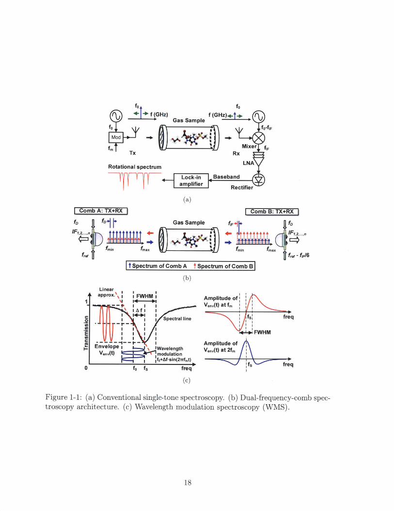
1-1 (a) Conventional single-tone spectroscopy. (b) Dual-frequency-comb
spectroscopy architecture. (c) Wavelength modulation spectroscopy
(W M S) . . . . . . . . . . . . . . . . . . . . . . . . . . . . . . . . . . 18
2-1 (a) THz signal with two phase noise sidebands probes the spectral line
and (b) The generated signal and PM-to-AM noise on the baseband. 26
2-2 Minimum detectable absorption coefficient 'gas,MIN and optimum length
of gas cell L,,pt and for spectrometers with different waveguide loss. . 30
3-1 (a) Circuit architecture of the CMOS spectrometer and each active
molecular probe (AMP). (b) Backside radiation through a hemispheric
silicon lens. . . . . . . . . . . . . . . . . . . . . . . . . . . . . . . . . 35
3-2 Advantages of the presented comb spectrometer: (a) comparison with
other state-of-the-arts silicon circuits above 200 GHz in terms of ra-
diated power versus bandwidth and (b) the total energy consumption
versus bandwidth. . . . . . . . . . . . . . . . . . . . . . . . . . . . . . 36
3-3 A 3D view of the core of the active molecular probe (AMP). . . . . . 37
3-4 (a) Odd-mode signal flow of the AMP at the fundamental frequency
fo. (b) Schematic of the equivalent half circuit. . . . . . . . . . . . . 38
3-5 The simulated guided wavelength of Slot 1 at various frequencies. . 38
3-6 Simulated electrical field distribution of the AMP at (a) fo=137.5 GHz
with differential mode signal on the drain connectors and (b) 2fo=275 GHz
with common mode signal on the drain connectors. . . . . . . . . . . 39
3-7 Anatomy of transistor embedding network using dual-transmission-line
(DTL) feedback. . . . . . . . . . . . . . . . . . . . . . . . . . . . . . 41
9
3-8 Simulated U/A movement with DTL feedback on gain plane with (a)
constant Gma contour (b) constant K contour. . . . . . . . . . . . . . 43
3-9 (a) Simulated impedance-matched power gain of a MOS transistor with
and without the dual-transmission-line (DTL) feedback. (b) Simulated
doubler efficiency with and without DTL at 275GHz. . . . . . . . . . 43
3-10 Simulated optimum matched load impedance and stability factor for
the 275-GHz AMP under different Gina (in linear scale) . . . . . . . . 44
3-11 (a) Simulated realized power gain of the AMP at 275 GHz versus the
length of Slot 1. (b) Simulated antenna efficiency, doubler efficiency
and total efficiency of the AMP at 275 GHz with various lengths of
S lot I. . . . . . . . . . . . . . . . . . . . . . . . . . . . . . . . . . . . 4 5
3-12 (a) Even-mode signal flow of the AMP at the 2"d-harmonic frequency
2fo. (b) Simulated radiation pattern of the AMP. . . . . . . . . . . . 48
3-13 (a) Sub-harmonic mode operation and IF extraction. (b) Simulated
single-sideband noise figure of the AMP. . . . . . . . . . . . . . . . . 49
3-14 Slot balun design: (a) physical structure and electrical-field distribu-
tion, (b) schematic, (c) simulated S-parameters, and (d) simulated
output amplitude and phase errors. . . . . . . . . . . . . . . . . . . . 49
3-15 (a) Schematic, (b) 3D view and simulated output spectra of the SSB
up/down-conversion mixers. . . . . . . . . . . . . . . . . . . . . . . . 51
3-16 (a) Schematic and (b) simulated output power of the 135-GHz input
frequency tripler (Pi,=6 dBm). . . . . . . . . . . . . . . . . . . . . . 52
4-1 Photograph of: (a) CMOS THz comb transceiver based on 65-nm bulk
CMOS process (2x3 mm2 ) and (b) the packaged chip on PCB with
1-inch diameter silicon lens attached at the backside. . . . . . . . . . 56
4-2 Experimental setup for the characterization of spectrum, radiation pat-
tern and radiated power. . . . . . . . . . . . . . . . . . . . . . . . . . 57
4-3 The measured spectrum of 10 comb lines from 225-to-315GHz with
10-G Hz spacing. . . . . . . . . . . . . . . . . . . . . . . . . . . . . . . 57
4-4 Measured radiation pattern of one output channel (265 GHz). .... 57
10

4-5 Measured (a) EIRP and (b) phase noise of the frequency comb line
output (represented by different colors) . . . . . . . . . . . . . . . . . 58
4-6 Experimental setup for the characterizations of conversion gain and
noise figure. . . . . . . . . . . . . . . . . . . . . . . . . . . . . . . . . 59
4-7 (a) Measured single sideband conversion gain and (b) measured single
sideband noise figure of each frequency comb channel. . . . . . . . . . 60
4-8 (a) Schematic and (b) photograph of THz spectroscopy setup. . . . . 61
4-9 Measured spectrum of OCS using WMS at f,: (a) full band spectrum
versus the recorded integrated intensity (LGINT) from JPL molecu-
lar catalog and (b) details of OCS spectral lines at 231.061 GHz and
316.146 GHz, respectively. . . . . . . . . . . . . . . . . . . . . . . . . 63
4-10 Measured spectrum of of CH3CN using WMS at fm versus the inte-
grated intensity (LGINT) from JPL molecular catalog: (a) full band
spectrum and (b) details of two spectral sections located at 220.2-to-
220.8 GHz and 312.1-to-312.7 GHz, respectively. . . . . . . . . . . . . 64
4-11 SNR,/, variation versus pressure degradation for the 279.685 GHz spec-
tral line of OCS and the 294.251 GHz spectral line of acetonitrile
(A v= 78 H z). . . . . . . . . . . . . . . . . . . . . . . . . . . . . . . . 65
4-12 Measured spectrum of CH3CN and OCS gas mixture using WMS at
2fm : (a) full band spectrum. (b) details of 231.061 GHz and 316.146 GHz
spectral lines of OCS in the mixture. (c) details of 220.2-to-220.8 GHz
and 312.1-to-312.7 GHz spectral lines of CH3CN in the mixture. . . . 67
11

12

List of Tables
2.1 Detection Sensitivity of Various Gases . . . . . . . . . . . . . . . . . 31
5.1 Performance Comparison of Rotational Spectrometer . . . . . . . . . 70
13

14

Chapter 1
Introduction
1.1 Rotational Spectroscopy for Gas Sensing
Ultra sensitive gas sensing is of great importance in environmental monitoring, indus-
trial process control, hazardous agent detection, etc. [1]. It is also gaining increasing
interests in clinical disease diagnosis. One important application is the molecular
analysis of human exhaled breath [2, 3], which contains abundant volatile organic
compounds (VOCs). Many of these VOCs, with concentrations ranging from ppm
to ppb levels, have unique physiological basis [4, 5]. For example, hydrogen sulfide,
acetone and toluene have strong correlation with halitosis, diabetes and lung cancer,
respectively.
Current technologies for gas sensing includes: (1) gas chromatography/mass spec-
troscopy (GC/MS), which achieves ppb level sensitivity with pre-concentration tech-
niques. However, it is ineffective for the identification of different compounds with
similar mass spectra [5]; (2) selected-ion flow-tube mass spectroscopy (SIFT-MS)
and proton transfer reaction-mass spectrometry (PTR-MS) , which detect ionized
molecules produced by gas-phase collisions. They have ppt level sensitivity but the
specificity is also limited; (3) mid-Infrared spectroscopy [6] detects the vibrational
spectrum of gas molecules, which is sensitive due to the strong absorption intensity
in infrared range. However, the limited tunability and linewidth of the light source
make it less effective for complicated mixture analysis; (4) MEMS resonator based
chemical sensors [7, 8, 9], which measure the variation of resonate frequency after
15

absorption of gas molecules, have promising mass resolution but still suffer from se-
lectivity issue; (5) electrochemical sensors, which is low cost but can only detect
specific chemical species.
Rotation of polar gaseous molecules have quantized energy states in millimeter-
wave and THz range. When molecules are excited by electromagnetic waves with
photon energy matching that of the rotational state transitions, absorption spectral
lines can be measured [10, 11]. The absorption intensity, as a result of degener-
ated quantum state number (increase with frequency) and probability for unoccupied
quantum states (decrease with frequency), peaks at low-THz frequencies for most
gaseous molecules. THz rotational spectroscopy is a powerful tool for gas sensing
over the aforementioned technologies for the following reasons:
1. Simultaneous identification/analysis for a wide range of molecules is enabled
through broadband scanning. "Molecular spectral lines all follow a quasi-periodic
pattern in frequency domain, and the "period" is determined by the dipole mo-
ment, weight, etc. of molecules. In fact, a spectroscopic bandwidth of 100 GHz
allows the coverage of most of the chemical species under interest, including
very light molecules such as hydrogen cyanide (HCN), which has a repetitive
spectral line every 88.61 GHz [12].
2. The width of spectral lines in the Doppler-limited regime (at low pressure) is
around 1 MHz. The corresponding spectral-line quality factor of Q~10' leads
to ultra-high detection specificity. Spectral overlap from different molecules is
highly unlikely. The sub-kHz frequency resolution (at least 3 orders lower than
the spectral line width) is also supported by nowadays THz electronics. Both
of the narrow spectral lines and high quality THz signal sources make THz
spectrometers capable of analyzing complex gas mixtures in details.
3. Previously, sensitive THz spectrometers using discrete compound III-V semi-
conductor components are reported. Working in conjunction with a widely
adopted, industrial standard gas pre-concentration gain of 105, ppt-level sensi-
tivity is achieved [13], which is comparable with state-of-the-art gas sensors.
Recently, rapid development of silicon-based THz integrated circuits brings about
new opportunities for low-cost, energy-efficient rotational spectrometers at chip scale.
16

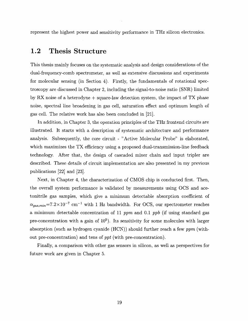
As shown in Fig. 1-1(a), the spectrometer architecture widely adopted in prior arts
performs molecular probing using a single tunable tone [14, 15, 16, 17]. Although
relatively compact and convenient to implement, it has several disadvantages: (1) the
full-band scanning is time consuming. To scan a 100-GHz bandwidth with 10-kHz
resolution and 1-ms integration time per point, it consumes ~3 hours in total. (2)
It suffers from power efficiency and sensitivity degradation due to the need for lossy
tunable components and low Q-factor resonators to deliver broadband coverage. (3)
The maximum radiation power density for probing is set by the molecular saturation
effect. As a result, an upper speed limit exists for this architecture due to the max-
imum achievable signal-to-noise ratio (SNR) per frequency step. Besides single-tone
spectrometers, a 260 GHz pulse-based radiator with 24.7 GHz bandwidth for spec-
troscopy has been implemented [18]. However, due to the low duty cycle of pulse
modulation, 80% of the RF energy is lost, which leads to low SNR. Without phase
locking, it also lacks kHz-level tunability. Pulsed echo spectrometer [19] reduces the
required RF power. But it needs to mechanically adjust resonant frequency of the
cavity, which slows down the scanning speed. The reported frequency accuracy of its
signal source is 0.1 ppm or 10 kHz. In [20], THz comb is generated through nonlinear
optics using periodic laser pulses. This approach provides abundant comb lines from
100 GHz to 2 THz with frequency interval of 250 MHz. However, it comes with lower
average radiated power and insufficient frequency resolution (~25 MHz).
In this thesis, a 220-to-320 GHz, dual-frequency-comb spectrometer in 65-nm bulk
CMOS process is presented. As shown in Fig. 1-1(b), the spectrometer probes the
gas molecule sample using two counter-propagating comb signals rather than a sin-
gle tunable tone. Each radiated comb signal has 10 continuous-wave, evenly-spaced
frequency tones. Generation and heterodyne detection of the two comb signals are
conducted simultaneously. The two comb spectra can also be shifted, so that a 100-
GHz bandwidth is seamlessly covered. Through the parallel spectral scanning with
the 20 comb lines, the scanning speed is enhanced by a factor of 20 x. Since each comb
line sweeps within only a small fractional bandwidth, peak efficiency is maintained,breaking the aforementioned bandwidth-efficiency trade-off in single-tone spectrome-
ters. The measured silicon chip achieves state-of-the-art 5.2-mW radiated power and
14.6-19.5 dB single sideband noise figure (SSB NF). To our best knowledge, these
17
fof (G
foMod
Tx
Rotational spectrum
Comb A: TX+RX
foHz) f (GHz)4}+ *
Gas Sample 'fo-fIF
R Mixer fIF
Rx
LNA
Lock-in Basebandamplifier Rectifier
(a)
Comb B: TX+RX
fD j DI Gas Sample Lj fD
,.L+ ++ IF1,2,...,n
rin fmax fmin fmaxfff fr. - fI46
t Spectrum of Comb A t Spectrum of Comb B
(b)
Linearapprox. FWHMi
Spectral line
-- -i -- t-- IEnvelope i IWavelengthVenv(t) modulation
I fo+Af-sin(2Tfmt)
fo fs freq
(c)
Amplitude of'Ve.v(t) at fm
ts ~ freq
FWHM
Amplitude ofVen,(t) at 2fm
|fs freq
Figure 1-1: (a) Conventional single-tone spectroscopy. (b) Dual-frequency-comb spec-troscopy architecture. (c) Wavelength modulation spectroscopy (WMS).
18
-)
0
represent the highest power and sensitivity performance in THz silicon electronics.
1.2 Thesis Structure
This thesis mainly focuses on the systematic analysis and design considerations of the
dual-frequency-comb spectrometer, as well as extensive discussions and experiments
for molecular sensing (in Section 4). Firstly, the fundamentals of rotational spec-
troscopy are discussed in Chapter 2, including the signal-to-noise ratio (SNR) limited
by RX noise of a heterodyne + square-law detection system, the impact of TX phase
noise, spectral line broadening in gas cell, saturation effect and optimum length of
gas cell. The relative work has also been concluded in [21].
In addition, in Chapter 3, the operation principles of the THz frontend circuits are
illustrated. It starts with a description of systematic architecture and performance
analysis. Subsequently, the core circuit - "Active Molecular Probe" is elaborated,
which maximizes the TX efficiency using a proposed dual-transmission-line feedback
technology. After that, the design of cascaded mixer chain and input tripler are
described. These details of circuit implementation are also presented in my previous
publications [22] and [23].
Next, in Chapter 4, the characterization of CMOS chip is conducted first. Then,
the overall system performance is validated by measurements using OCS and ace-
tonitrile gas samples, which give a minimum detectable absorption coefficient of
%as,min=7.2x10⁻⁷ cm-1 with 1 Hz bandwidth. For OCS, our spectrometer reaches
a minimum detectable concentration of 11 ppm and 0.1 ppb (if using standard gas
pre-concentration with a gain of 105). Its sensitivity for some molecules with larger
absorption (such as hydrogen cyanide (HCN)) should further reach a few ppm (with-
out pre-concentration) and tens of ppt (with pre-concentration).
Finally, a comparison with other gas sensors in silicon, as well as perspectives for
future work are given in Chapter 5.
19

20
Chapter 2
Performance Analysis of A
Spectroscopic System
Sensitive spectrometer design requires a comprehensive consideration for the on-chip
electronics, molecular properties, gas cell, and their interactions. Systematic analysis
and optimizations of these factors will be presented in this chapter. As is shown
later in Section 3.1, the generation and detection of each comb frequency tone are
performed by a THz transceiver unit in each comb chip (Fig. 3-1(a)). For each pair
of comb tones, the circuit operation are the same as a typical single-tone heterodyne
spectrometer shown in Fig. 1-1(a). In mmW/terahertz range, cascaded heterodyne
receiver and square-law detector are preferable over direct square-law power detection
due to its higher sensitivity. Normally, standing wave is formed inside the gas cell,
which is due to multi-reflection between the inlet and outlet THz-signal windows. It
introduces significant periodic RF power variation in frequency domain. The length
of gas chamber is about A/2 of the RF power variation frequency (70 cm gas cell
for a variation frequency of 214 MHz). Thus, even if no spectral lines exist, the
system has a baseline fluctuation. Wavelength modulation spectroscopy (WMS) [24]
with a modulation frequency of fm and a deviation frequency of Af (illustrated in
Fig. 1-1(c)) is adopted, which measures the derivatives of the overall transmission
response. Since the derivatives (especially the 2n-order derivative) of the baseline
are much smaller than that of the spectral lines, this approach effectively reduces the
impact from the baseline fluctuation. In addition, for maximum baseband response,
21

Af is chosen to be half of the full width at half maximum (0.5 x FWHM) of the
spectral line (for output at fin) or FWHM (for output at 2fm ), respectively. Note
that analyses throughout this section are based on single-channel circuits (Fig. 1-1(a))
and the above detection principles, but are also applicable to our comb spectrometer.
2.1 Impact of Receiver Noise on Sensitivity
In Fig. 1-1(a), the received signal power changes according to the gas absorption
intensity, which can be expressed as:
O= Pe-oL - a L) oe Lagas L, (2.1)
where P is the transmitted signal power, agas is the peak absorption coefficient at
the center of spectral line, ao and L are the path loss coefficient and length of the
gas cell. Here, we assume agasL < 1 given the normally low molecule concentration,
and no extra loss exists besides path loss and gas absorption.
Next, the overall receiver noise is dominated by the input-referred noise temper-
ature T,=TO(F - 1) of the mixer, where F is the mixer noise factor, and To is the
ambient temperature. Therefore, the RMS noise voltage referred at the receiver input
side is Vn,RMS =V/kTnfENBWZo, where k is Boltzmann's constant, ZO is receiver input
impedance and fENBW is the effective noise bandwidth. To investigate its impact on
detection sensitivity, we note that the total voltage at the square-law detector input
is:
Vi(t) = [Vo sin(wot) + vn(t )] Gixer, (2.2)
where V is the amplitude of the receiver input voltage (and equals to 2ZoPoe-aOL
if no gas exists) and Gmixer is the mixer conversion gain. Meanwhile, the square-law
detector is modeled as a polynomial function:
Vout(t) = C1 Vin(t) + C2 Vin(t) 2 + C3Vin(t) 3 + ... (2.3)
22
As a result, the final baseband output of the square law detector is:
Vot= C2 Gjize,[YP + 2Vo sin(wot )vfl(t|BB + - - -1 ( 2.4)2
The low-pass-filtered detector output signal is then:
V 2VS, 0ut = C2Glix, 2 (2.5)
Within an output bandwidth of Av at baseband, the second term in (2.4) repre-
sents a down-conversion of both the upper and lower RF sideband noise v" around
w0 (i.e. fENBW= 2 Av). Therefore, in (2.3) the total integrated noise (RMS) at the
detector output is:
Vn,out = C2 G i, V" 2kTnAVZO. (2.6)
Equation (2.6) is also called Townes noise [10], which is dependent on the input
signal power level. If assuming no gas absorption, the baseband SNR (in voltage) of
the receiver, with a bandwidth of Av, is then:
= -t 2 V 2 1 poe-aoLSNRBB lvv T -,2Tt (2.7)
Vn,out 2 Vo 2k, v Zo 2 kTAav'
A few conclusions are made out of the above derivations:
1. The ratio between the input RF signal power and the input-referred receiver
noise with the same bandwidth of Av is:
Pe-a L (2.8)SN RRF v/v 0 -0-:
By comparing (2.7) with (2.8), we see that an SNR degradation of 2x or 6 dB
occurs. This, verified by our circuit simulation, is important for sensitivity esti-
mation based on electronic RF performance and is later used in our experiments
(Chapter 4).
2. Here, the shot noise of the detector is not included, but will ultimately limit the
SNR even if the transmitter and receiver mixer are noise-free. Shot noise results
23

from the charge injection over semiconductor barrier in the detector diode. Its
current spectral density is i2 = 2qeIDcAv, where q, is the charge of electron,
and IDC is the rectified DC output current. The associated ultimate SNR is
therefore:
SNRBB,ShotNoise -DC (2.9)2qAv*
Note that the current responsivity of a diode is ~ 10 A/W, meaning that 0.1 mW
of input power already leads to an SNRBB,ShotNoise of 5.6x 10 7, or 160 dB with
baseband bandwidth of Av=1 Hz. This is a few orders of magnitude larger
than the SNR typically achieved by a THz frontend (see Section 4). Therefore,
our THz spectrometer is not shot-noise limited.
3. In case of detection with modulation frequency fm and frequency deviation
Af = 0.5 x FWHM, the system researches maximum baseband SNR at fm
when the RF center frequency is fo = f, 0.5 x FWHM, if a linear approxima-
tion rather than Lorentz or Gaussian profile is assumed, as shown in Fig. 1-1(c).
The maximum baseband SNR is expressed as:
SNRBB v/v _- s'Out
(2.10)1 Poe-aoL -gas L
2 k~Av(1-e- 2 ).2kTnAv
If agasL < 1, (2.10) is simplified as:
1 Poe-aoLSN RBBvv 1_ k agasL. (2.11)
4 kTnAv a
It indicates that when agasL<1 the molecule concentration (linearly propor-
tional to agas) is linearity proportional to the input/output SNR in voltage
rather than in power. That means, for example, even if the receiver noise figure
is reduced by 20 dB, the sensitivity of the spectrometer (in terms of ppx) is only
improved by 10 x. This is later verified by our experiments in Fig. 4-11. In addi-
tion, it should also be noticed that due to the non-ideal profile of spectral lines,
24
the expression of actual SNR differs slightly from (2.11). For instance, 2 dB
SNR degradation is expected for a Lorentzian profile (pressure induced broad-
ening), and 0.6 dB SNR degradation is expected for Gaussian profile (Doppler
limited broadening). However, this error can be compensated by choosing a
slightly larger Af. Lastly, (2.11) can also be applied to the detection output at
2fm with Af = FWHM, where ~3 dB lower SNR compared with WMS at fm
is obtained at the center frequency of spectral line (fe, in Fig. 1-1(c)).
2.2 Impact of Transmitter Noise on Sensitivity
The amplitude and phase noise of the transmitter may also affect the sensitivity. To
investigate this issue, we assume that the receiver is noiseless, and the IF signal, being
a frequency-shifted version of the transmitted signal, is:
Vin(t) = [Vo + an(t)] cos[wot + On~(t)] -Gmixe,, (2.12)
where V, an(t), wo and #n(t) are the signal amplitude, amplitude noise, carrier fre-
quency and phase noise, respectively. The phase noise On(t) = OP sin(27rfmt) is as-
sumed to have a sinusoidal form [25], where , is the peak phase fluctuation, and
27rfm is the offset frequency from wo.
First, if an input signal contains only phase noise (an(t) = 0), and the phase noise
is assumed small, (2.12) is then written as:
Vin (t)= Vo cos[wot + , sin(27rfmt)] - Gjixer
~ VGmixer{COS(WOt) - -[cos(wo - 27rfm)t (2.13)2
- cos(wo + 27rfm)t]}
The 2 nd and 3 rd items of (2.13) refer to the two phase noise sidebands (upper
sideband (USB) and lower sideband (LSB) as shown in Fig. 2-1(a)). If no spectral
lines exist at the probing frequency, the amplitudes of two sidebands are equal. After
the square-law detection, the two sideband signals will cancel each other. As a result,
25
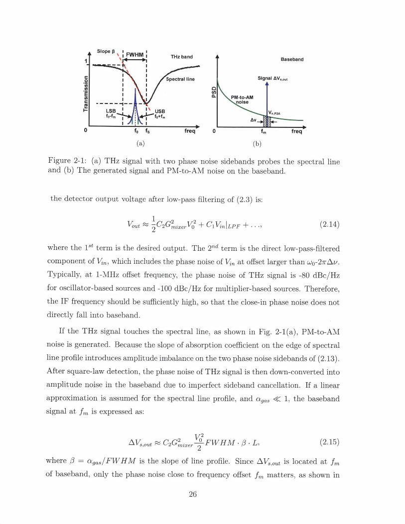
Slope FWHM i THz band Baseband
Spectral line Signal AV, 0 t
0)0a.40 PM-to-AM
.C noise
LSB USB VnP2A
Av
0 f0 fs freq 0 fm freq
(a) (b)
Figure 2-1: (a) THz signal with two phase noise sidebands probes the spectral lineand (b) The generated signal and PM-to-AM noise on the baseband.
the detector output voltage after low-pass filtering of (2.3) is:
1Vout C 2 GnixerV0
2 + C1Vin LPF + (2.14)2
where the 1" term is the desired output. The 2nd term is the direct low-pass-filtered
component of VL, which includes the phase noise of V, at offset larger than wo-27rAv.
Typically, at 1-MHz offset frequency, the phase noise of THz signal is -80 dBc/Hz
for oscillator-based sources and -100 dBc/Hz for multiplier-based sources. Therefore,the IF frequency should be sufficiently high, so that the close-in phase noise does not
directly fall into baseband.
If the THz signal touches the spectral line, as shown in Fig. 2-1(a), PM-to-AM
noise is generated. Because the slope of absorption coefficient on the edge of spectral
line profile introduces amplitude imbalance on the two phase noise sidebands of (2.13).
After square-law detection, the phase noise of THz signal is then down-converted into
amplitude noise in the baseband due to imperfect sideband cancellation. If a linear
approximation is assumed for the spectral line profile, and aga, < 1, the baseband
signal at fm is expressed as:
V2AV"t~ C2Gixer FWHM - 0 - L, (2.15)
where 3 = ags/FWHM is the slope of line profile. Since AV,,Out is located at fm
of baseband, only the phase noise close to frequency offset fm matters, as shown in
26
Fig. 2-1(b). Based on (2.3) and (2.13), the PM-to-AM noise at fm of baseband is
then expressed as:
V2 fm~4L (2.16)Vn,P2 A ~C2GMixeri 4m-p.L .6
The SNR in voltage due to PM-to-AM noise can then be calculated using the
following equation:
FWHMSNRP2A v/v f f"Av/ 2 PNSSB (v)d (2.17)
where PNSSB (v) is the single sideband phase noise of THz signal at frequency offset
v, and Av is integration bandwidth. Thus, for one spectral line with FWHM of
1 MHz, f m of 50 kHz and Av of 1 Hz, the phase noise at 50 kHz frequency offset
needs to be at least -54 dBc/Hz for SNR of 104. But since Vn,P2A decreases linearly
with molecule concentration (i.e. smaller 3), PM-to-AM noise only matters under
high SNR. It is not a limiting factor for sensitivity, which is defined when SNR=1.
Next, if the input contains only amplitude noise (i.e. 0,(t) = 0), it is similar to
the input referred noise of receiver as shown in (2.4):
2 2V ~C2Gr2n ' + Van(t ) + an (t )2)+...(2.18)
We note that Townes noise in the 2 nd term is again the dominant noise contributor,
which results from the close-in amplitude noise of the transmitter signal. Fortunately,
many mmW/terahertz CMOS sources (including ours) are based on heavily-driven
nonlinear devices. The voltage swing of these devices is normally saturated or clipped
by the power supply rail, which in turn suppresses the amplitude fluctuation caused
by device noise. In addition, the power supply noise can potentially modulate the gain
of transceiver and introduce amplitude noise to the baseband, and should therefore
be maximally suppressed in the design of the entire system. Currently the noise
of the receiver still dominates the overall SNR. In the future, however, when THz
amplifier (with no squeezing of amplitude noise) becomes available, this issue should
be revisited.
27

2.3 Spectral Broadening and Effect of Gas Cell
Size
Both the inter-molecular collision (i.e. pressure) and the Doppler effect of Brownian
motion cause spectral broadening. To achieve absolute specificity, gas pressure should
be sufficiently low, so that the linewidth is only limited by Doppler effect, in order
to avoid spectral-line overlap. It is noteworthy that optimum pressure increases with
frequency [10], and in mmW/terahertz range, such pressure threshold is -10 Pa.
In addition, when encapsulated inside a gas cell, molecules also have collisions with
the sidewalls of gas cell, leading to additional broadening. Fortunately, this is not
a predominant concern for THz spectrometer. Note that a spectral-line absorption
y(f) due to collision follows a Lorenzian profile [26]:
1/27r(
W (f - fo) 2 + (1/27rT)2'
where fo is resonance frequency and T is the mean free time between molecular colli-
sions. The full width of half maximum (FWHM) of the spectral line is therefore ~ .
At the Doppler-limited pressure level (-10 Pa), the value of r is '~0.3 As (hence a
FWHM of ~1 MHz), and the mean free path of molecules, determined by molecular
diameter d and gas pressure P is:
_kT 0Ao = .o (2.20)v/-7rd2 p
As an example, the mean free path for OCS (d=8 A) is 140 Am. Even if a WR-
3.4 waveguide (aperture size of 860x430 pm2 ) is adopted as gas cell, which enables
propagation of a 220-320-GHz TEO, wave, its dimension is still a few times larger
than the above mean free path, and does not cause significant spectral broadening.
In fact, the gas cell in our setup is even -100x wider. Hence, the detection specificity
is not degraded.
28

2.4 Molecular Saturation and Maximum Allowable
Signal Power
High incident signal power may deplete the population of unexcited molecules, pre-
venting additional photon absorption if the signal power is further increased. Such
saturation effect, occuring at the tip of the spectral line first, not only leads to spec-
tral broadening, but also nonlinear dependency between power absorption and gas
concentration. The maximum probing signal power flux I can be estimated by [10]:
3coch 2(Af) 2
j = (2.21)D2'
where co is the permittivity of vacuum (8.85x 10⁻¹² F/m), c is the speed of light
(3 x 10⁸ m/s), h is Planck's constant (6.6 x 10- 34 J.s), D is molecular dipole moment,
and Af is the absorption linewidth. The dipole moment of most polar molecules is
on the order of 1018 esu (in CGS system) or 3.3x10- 3 0 C-m. Hence, the saturation
power flux of a low-THz spectrometer is -0.3 mW/mm 2 . Normally, the gas cell
cross-sectional area is large enough that power saturation is avoided; however, if
a single-mode WR-3.4 waveguide is used for sensor miniaturization, the maximum
allowable signal power reduces to ~0.1 mW, which is achievable in CMOS circuits
(including our chip). This poses a fundamental limit for the SNR (shown in (2.11))
that a single-tone spectrometer can provide. In Section 3.1.3, it will show how this
problem is addressed by the comb spectrometer.
2.5 Optimum Path Length of Gas Cell and Maxi-
mum Achievable Sensitivity
The minimum detectable gas absorption coefficient agas,min is derived when the spec-
trometer baseband SNR (shown in (2.11)) is unity:
4 kTn/Avagas,min L Poe-aoL. (2.22)
A longer gas cell path length L enables stronger absorption but also higher waveg-
29

4 100
E 800 3 \
S60 EX 2-',
40 -
22 ------- 20SCO Dielectric Metal
0 Waveguide Wavequide, 00.02 0.04 0.06 0.08 0.1
Transmission Line Loss a0 (cm 1 )
Figure 2-2: Minimum detectable absorption coefficient agas,MIN and optimum lengthof gas cell Lpt and for spectrometers with different waveguide loss.
uide power loss. In (2.22), an optimum length Lpt exists to achieve the minimal value
of agas,min. By having dgas"min(L) =0, we derive:dL
Lopt - , (2.23)a0
and the ultimate agas,min achievable by the electronics is:
agas,MIN = 2ea T (2.24)P0
Therefore, the minimum detectable gas concentration is expressed as:
=gas,MIN 2ea0 kTnZv (2.25)'Ymin - -(.5agas,pure agas,pure 0
where agas,pure is the absorption coefficient of pure gas sample.
Currently, most THz spectrometers are based on the propagation of a collimated
Gaussian beam inside a bulky gas cell. In the future, if single-mode metal rectangular
waveguide is adopted as gas chamber, the optimum gas cell length Lopt and the asso-
ciated minimum detectable absorption intensity agas,MIN, as a function of path loss
a0 , are plotted in Fig. 2-2. Here, a signal power of 0.1 mW is assumed, which is the
threshold power for molecular saturation (Section 2.4). A single sideband noise figure
(NF) of 17 dB is assumed. Both metrics are achieved by our CMOS comb spectrome-
30

Table 2.1: Detection Sensitivity of Various GasesGas Line Freq.1 Absorption Detection
(GHz) Intensity 2 (cm- 1 ) Sensitivity (xppm)
carbonyl sulfide (OCS) 292.04 0.048 @ 13 Pa 0.3
dinitrogen monoxide (N 2 0) 301.65 6.3 x 10- 3 @ 27 Pa 2.5
carbon monoxide (CO) 228.60 2.3x10⁻³ @ 40 Pa 6.8
nitric oxide (NO) 250.62 1x10⁻³ U 40 Pa 16
sulfur dioxide (SO 2 ) 283.68 0.012 9 4 Pa 1.3
nitrogen dioxide (NO 2 ) 256.16 7x10- 4 13 Pa 22
formaldehyde (H 2 CO) 301.04 0.047 ( 4 Pa 0.2
hydrogen cyanide (HCN) 266.07 0.2 0 2 Pa 0.08
methanol (CH 30H) 318.54 5x10- 3 4 Pa 3.1
1 Listed molecules normally have more than one spectral lines in the 220-320-GHz range. Only one linewith high absorption intensity is selected here.
2 Different molecules have different optimum detection pressure. The absorption intensity and detectionsensitivity here are determined at the optimum pressure of each gas.
3 Integration bandwidth Av=1 Hz, To=296 K, no pre-concentration techniques is assumed.
ter (see Section 4). For a typical waveguide loss of 0.25 dB/cm (i.e. a0=0.058 cm- 1),
the minimum detectable absorption intensity agas,MIN is 1.6X 10⁻⁸ cm- 1 with 1 Hz
bandwidth at 296 K. The optimum gas cell length is ~35 cm. Table 2.1 shows the sen-
sitivity or minimum detectable gas concentration based on the calculated minimum
detectable absorption coefficient. A sensitivity at ppm level is predicted. A standard
pre-concentration gain of 105 (like the one used in [13]) will further increase the spec-
trometer sensitivity to ppt level. According to Fig. 2-2, if low-loss hollow dielectric
waveguide is used, the sensitivity can be further improved by 2~3x. Although the
gas cell waveguide has an optimum length of 0.1-1 m, they can be folded to shrink
the size of the spectroscopy system (in conjunction with the usage of micro vacuum
pumps).
31

32
Chapter 3
The Sub-THz
Dual-Frequency- Comb
Spectrometer
3.1 Overview of the CMOS THz Spectrometer
3.1.1 Dual-Frequency-Comb, Bi-Directional Spectroscopy
Compared to the conventional single-tone spectral scanning scheme (Fig. 1-1(a)), the
presented dual-frequency-comb architecture (Fig. 1-1(b)) channelizes the detection
band by two identical frequency-comb chips with a 950-MHz frequency offset fIF
between their output radiation spectra. Each chip works under Tx and Rx modes
simultaneously. From Chip A, 10 equally-spaced comb lines with 10-GHz frequency
interval are transmitted through the gas sample and coupled into Chip B through
on-chip antennas. Meanwhile, inside Chip A, the above 10 comb lines are also used
as local-oscillator (LO) signals for the heterodyne mixing of another 10 comb lines
radiated from Chip B. Lastly, the 10 x 2 down-converted output signals at fIF, which
carry absorption spectral information of the gas, are extracted from the two chips. To
fully cover the 100-GHz bandwidth, the spectra of the comb pair only need to sweep
by 10 GHz. Lastly, it is noteworthy that similar channelized transceiver schemes were
also explored previously in impulse-radio ultra-wideband communications for pulse
shaping and spectral efficiency improvement [27, 28].
33
3.1.2 Architecture of The CMOS Comb Chip
A block diagram of the spectrometer is given in Fig. 3-1(a). Under the Tx mode, the
chip is driven by a tunable single-tone input signal, fret (45~46.67 GHz), which is
then tripled to 135~140 GHz and power divided into up- and down-conversion chains.
Through a series of cascaded single-sideband mixers, the chains produce signal tones
which are evenly spaced every 5 GHz. The 5-GHz frequency spacing is defined by a
frequency divider (÷2) with an external 10-GHz clock input, fD. Each single-tone
signal is then doubled by an active-molecular-probe (AMP) unit. Subsequently, the
10 comb lines located at 6fref+i-10 GHz (i=-5 to +4) are simultaneously radiated by
on-chip antennas built in the AMPs through a hemispheric silicon lens (Fig. 3-1(b))
attached at the backside of the chip. The lens suppresses the substrate mode and re-
duces reflection at its silicon-air interface. Finally, in the far field, the frequency comb
signal is achieved by the spatial combining of all radiation tones. Under the Rx mode,
the incident wave is coupled into the chip through the same reciprocal mechanism.
Sub-harmonic mixing is performed also in each AMP, of which the driving signal
behaves as LO. Compared to prior optical combs, which are based on mode-locked
laser pulse [29, 30], the CW-type electronic comb offers excellent tuning capability,
phase coherency (hence heterodyne detection), and high frequency resolution. This
architecture also enables scalability to higher bandwidth through extended cascading
of AMP channels.
3.1.3 Advantages of Dual-Frequency-Comb Spectrometer
Compared to prior optical combs based on mode-locked laser pulse [31, 32], the CW-
type electronic comb offers excellent tuning capability, phase coherency, and high
frequency resolution. It also enables scalability to higher bandwidth through ex-
tended cascading of AMP channels. In the dual-frequency-comb architecture, since
10 probing comb pairs work simultaneously, it leads to a much faster scanning speed
through parallel operation by at least a factor of 20x. In addition to that, significant
spectroscopic performance is gained, due to the following reasons.
Firstly, the chip architecture breaks the bandwidth-efficiency tradeoff of conven-
tional RF-to-THz designs, as mentioned in Section 1.1. By partitioning the overall
34

2f6-2f 2fo-3fD 2fo4fD 2f45fD
246D =2- X X I- Down-Conv.S1| I2 I3 - Chain
Down-Mixer Bufferfw: 45GHz Tripler-46.67GHz
fo=3fwa Up-Mixer
X F2 X2 j X2i~ IF2 X2 IF3 UpCoyl~a Up-Conv.-7 -1 - F4 Chain
2fo 2f4+fD 2f4+2f6 2fo+3f& 2f4+4f4
Active Molecular Probe (AMP)-- Tx 2f0+IfD
slotI Ba/un X2 F
Oi- 2 Bu ------..... Rx: 2fo+i-D+fF
AMP Core
(a)
1 O0GO
Raclat,wa',.
AWE CMVOS chip
HemisphericSilicon Lens - 320Gft* 4
(b)
Figure 3-1: (a) Circuit architecture of the CMOS spectrometer and each active molec-ular probe (AMP). (b) Backside radiation through a hemispheric silicon lens.
35

02 Radiated 0 On-wafer measured with
6 R 50% radiation efficiency -
This workE E c BW
0 [20] [10][21] Single-tone[-0% spectrometer .0
% [24] - . - EBW E do EcWu
[22] [23] [13] % ., [280 B001%[28] U -
[6 [25] 6 '- - . DFC spectrometer0 - [26] 0 0 [27]10 0- -- . Io 7 102 '
0 10 20 30 40 3 4 8 16 24 40Bandwidth (%) Bandwidth (%)
(a) (b)
Figure 3-2: Advantages of the presented comb spectrometer: (a) comparison withother state-of-the-arts silicon circuits above 200 GHz in terms of radiated powerversus bandwidth and (b) the total energy consumption versus bandwidth.
spectrum, the required tuning range for each channel is reduced below 4.5%, which
allows for high-Q topology (e.g. the dual-transmission-line feedback in AMPs) and
keeps peak performance across a broad frequency range. Shown in Fig. 3-2(a) is a
statistic of silicon-based sources above 200 GHz, which exhibits clear inversely pro-
portional dependency between the radiated power and bandwidth. In contrast, mywork demonstrates broad bandwidth without degrading the radiated power and noise
performance.
Secondly, as is discussed in Section 2.4, the maximum radiated power, is limited
by the saturation effect of molecules, especially for small-size gas cells. Subsequently,
it determines the ultimate sensitivity for a given total scanning time. In my comb, the
total radiated power exceeds such limitation while keeping each single tone still below
the saturation threshold. Given an fixed total scanning time and total bandwidth,since the integration time per frequency point is 20 x longer (i.e. smaller Av in (2.11))
due to the parallelism, the comb architecture achieves better sensitivity.
Thirdly, the energy efficiency is significantly improved. Due to the aforementioned
bandwidth-efficiency tradeoff, the total energy consumption of conventional single-
tone spectrometers has a square or cubic dependency over operational bandwidth
(Fig. 3-2(b)). In comparison, without extending scanning time, the energy consump-
tion of dual-frequency-comb spectrometer increases linearly with higher bandwidth
36
VD& Mixer Output @ fF
TX: 2fo -- - -----iiC RIF Choke
RX: 2fo+fF * Fo
L-_L @2fo
slot I --- -- --- -- -
Slot 2 -- ----:TL1 --- - -- --- -
@n ft Input -
Slot 3 TL2
VG
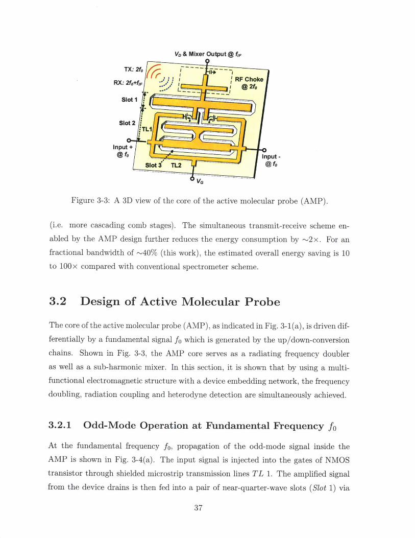
Figure 3-3: A 3D view of the core of the active molecular probe (AMP).
(i.e. more cascading comb stages). The simultaneous transmit-receive scheme en-
abled by the AMP design further reduces the energy consumption by ~2x. For an
fractional bandwidth of ~40% (this work), the estimated overall energy saving is 10
to 100 x compared with conventional spectrometer scheme.
3.2 Design of Active Molecular Probe
The core of the active molecular probe (AMP), as indicated in Fig. 3-1(a), is driven dif-
ferentially by a fundamental signal fo which is generated by the up/down-conversion
chains. Shown in Fig. 3-3, the AMP core serves as a radiating frequency doubler
as well as a sub-harmonic mixer. In this section, it is shown that by using a multi-
functional electromagnetic structure with a device embedding network, the frequency
doubling, radiation coupling and heterodyne detection are simultaneously achieved.
3.2.1 Odd-Mode Operation at Fundamental Frequency fo
At the fundamental frequency fo, propagation of the odd-mode signal inside the
AMP is shown in Fig. 3-4(a). The input signal is injected into the gates of NMOS
transistor through shielded microstrip transmission lines TL 1. The amplified signal
from the device drains is then fed into a pair of near-quarter-wave slots (Slot 1) via
37
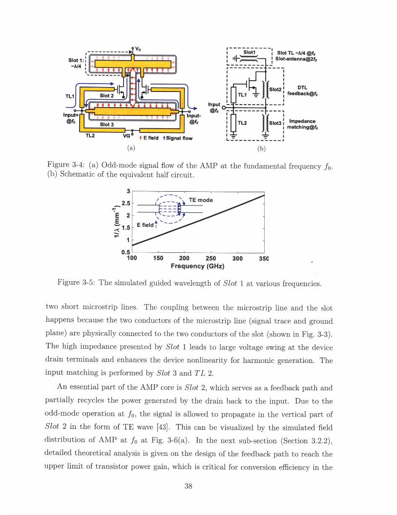
VD r -- -- - --- -- ISlot Slot TL -A/4 @fo
Slot-antenna@,2fo
oSlot2 DTLTL - feedback@fo
Input -@fo - - - - - - -Input+ Input- W
'ISrT2 o3 Impedanceo 3 1matching@fo
TL2 + E field tSignal flow LZ ------- -
(a) (b)
Figure 3-4: (a) Odd-mode signal flow of the AMP at the fundamental frequency fo.(b) Schematic of the equivalent half circuit.
/ - INTE mode2.5 -
1.5 -E field
0.5100 150 200 250 300 350
Frequency (GHz)
Figure 3-5: The simulated guided wavelength of Slot 1 at various frequencies.
two short microstrip lines. The coupling between the microstrip line and the slothappens because the two conductors of the microstrip line (signal trace and groundplane) are physically connected to the two conductors of the slot (shown in Fig. 3-3).The high impedance presented by Slot 1 leads to large voltage swing at the devicedrain terminals and enhances the device nonlinearity for harmonic generation. Theinput matching is performed by Slot 3 and TL 2.
An essential part of the AMP core is Slot 2, which serves as a feedback path andpartially recycles the power generated by the drain back to the input. Due to theodd-mode operation at fo, the signal is allowed to propagate in the vertical part ofSlot 2 in the form of TE wave [43]. This can be visualized by the simulated fielddistribution of AMP at fo at Fig. 3-6(a). In the next sub-section (Section 3.2.2),detailed theoretical analysis is given on the design of the feedback path to reach theupper limit of transistor power gain, which is critical for conversion efficiency in the
38

E Field [V/cm]
i.0088E+04
9. 1080E+03
8. 2000E+03
7.3000E+03
6.4000E+03
5.5000E+03
4. 6000E+03
3. 7000E+03
2.8000E+03
1. 9000E+03
.08O0E+03
(a) (b)
Figure 3-6: Simulated electrical field distribution of the AMP at (a) fo=137.5 GHzwith differential mode signal on the drain connectors and (b) 2 fo=275 GHz withcommon mode signal on the drain connectors.
frequency-doubler mode of AMP. To facilitate this analysis, the AMP circuit at fo is
translated into a half-circuit equivalence (shown in Fig. 3-4(b)). It is obtained based
on the symmetry of the circuit, where the central vertical line of the structure can beconsidered as virtual ground.
3.2.2 Double-Transmission-Line Feedback for Maximum Power
Gain (Gina) at fo
In order to improve the harmonic generation efficiency, the transistor power gainshould be maximized in order to reduce the input signal power. Meanwhile, thedevice should remain unconditionally stable in order to avoid self oscillation. For atwo-port linear network (e.g. a transistor or a transistor with embedding network),which is modeled by its Y-parameters
[Yo] Yii Y12 (3.1)Y21 Y22
the power gain Gina obtained through only input and output conjugate matching is
not the maximum achievable gain of the device. In [44], the following relationship
39
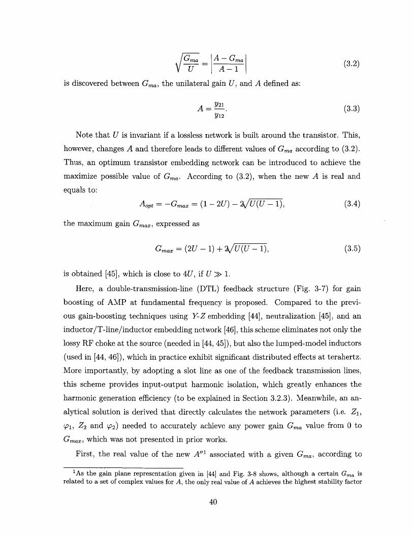
Ga A- Gma (3.2)U A-I
is discovered between Gma, the unilateral gain U, and A defined as:
A = Y21 (3.3)Y12
Note that U is invariant if a lossless network is built around the transistor. This,
however, changes A and therefore leads to different values of Gma according to (3.2).
Thus, an optimum transistor embedding network can be introduced to achieve the
maximize possible value of Gma. According to (3.2), when the new A is real and
equals to:
AOs = -Gmax = (1 - 2U) - 2U(U - 1), (3.4)
the maximum gain Gmax, expressed as
Gmax = (2U - 1) + 2/U(U - 1), (3.5)
is obtained [45], which is close to 4U, if U > 1.
Here, a double-transmission-line (DTL) feedback structure (Fig. 3-7) for gain
boosting of AMP at fundamental frequency is proposed. Compared to the previ-
ous gain-boosting techniques using Y- Z embedding [44], neutralization [45], and an
inductor/T-line/inductor embedding network [46], this scheme eliminates not only the
lossy RF choke at the source (needed in [44, 45]), but also the lumped-model inductors
(used in [44, 46]), which in practice exhibit significant distributed effects at terahertz.
More importantly, by adopting a slot line as one of the feedback transmission lines,
this scheme provides input-output harmonic isolation, which greatly enhances the
harmonic generation efficiency (to be explained in Section 3.2.3). Meanwhile, an an-
alytical solution is derived that directly calculates the network parameters (i.e. Z1,
W1, Z 2 and W2) needed to accurately achieve any power gain Gma value from 0 to
Gmax, which was not presented in prior works.
First, the real value of the new A"' associated with a given Gma, according to
'As the gain plane representation given in [44] and Fig. 3-8 shows, although a certain Gina isrelated to a set of complex values for A, the only real value of A achieves the highest stability factor
40
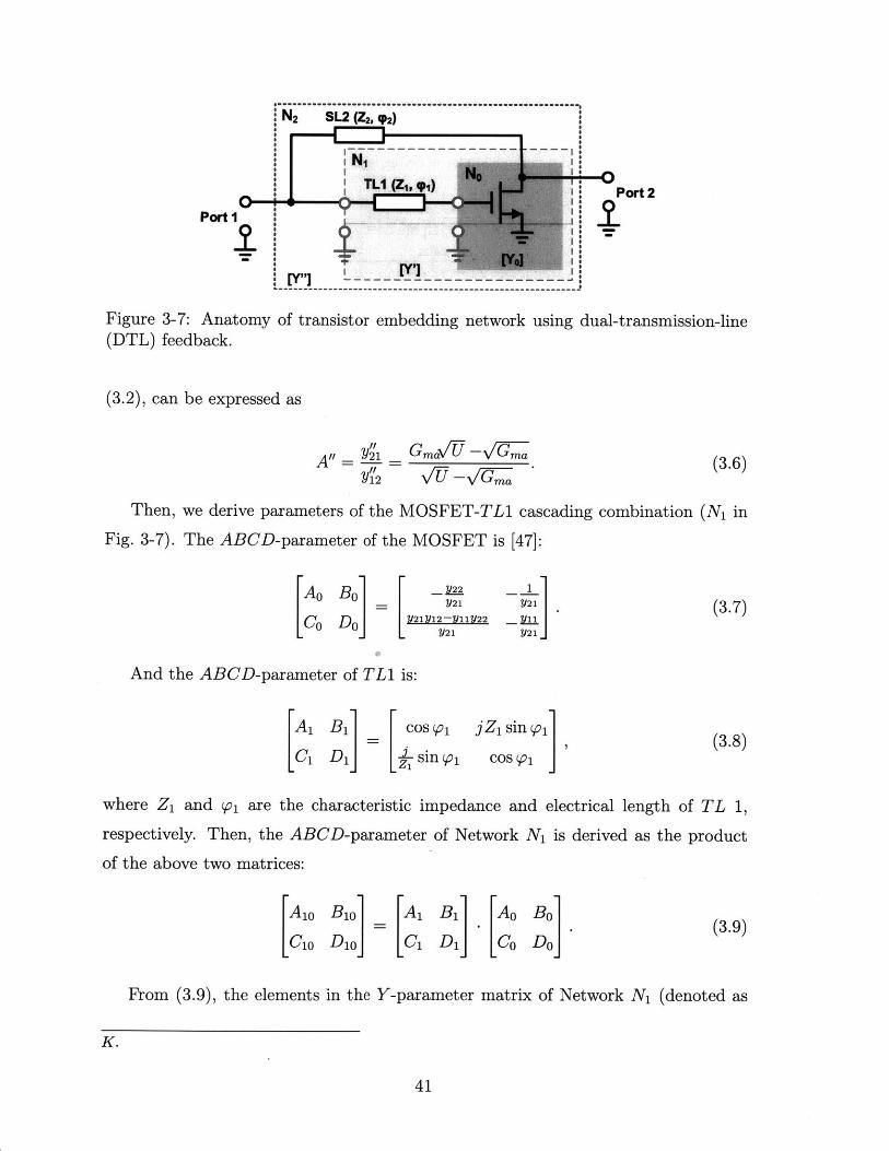
N2 SL2 (Z2, q2)
SN1SNo .TL1 (ZI, 91) 1 Pr
PPort 2
PoYrt 1
+ -'YJ I.
Figure 3-7: Anatomy of transistor embedding network using dual-transmission-line(DTL) feedback.
(3.2), can be expressed as
, y'1 GmaU -Gma (36)Y12 N-Gma
Then, we derive parameters of the MOSFET-TL1 cascading combination (Ni in
Fig. 3-7). The ABCD-parameter of the MOSFET is [47]:
Ao Bo - iL Y2" (3.7)Co Do Y21Y12111Y22 _ Y13
And the ABCD-parameter of TL1 is:
A1 B1 cos 1 jZ1 sin 1 (.(3.8)
C1 Di i sin (p1 cos 71
where Z1 and p1 are the characteristic impedance and electrical length of TL 1,respectively. Then, the ABCD-parameter of Network N is derived as the product
of the above two matrices:
A1 0 B1 A1 B1 Ao Bo
C10 Dio C1 D] Co Do (3.9)
From (3.9), the elements in the Y-parameter matrix of Network N (denoted as
K.
41
[Y'] in Fig. 3-7) are expressed as:
Yi =
Y12
sin (pi + COS '1 y11
COS 02 + jZ sin c1o- y.y12
cos pi + jZ 1 sin W, yiiy21
21 - cOsS91 + jZ1 sin 91 -yii
Y22 = Y22 -jZ2 sin (p -Y21Y12
COs (i + jZ sin o1 -yi
Next, the second transmission line SL2 (realized by Slot 2 in the AMP) is included.
Its Y-parameter is expressed as:
[YSL2] = Z s CO2 [ s2Z2 sin(P2 1
(3-11)-cos P21
where Z2 and 'P2 are its characteristic impedance and electrical length, respectively.
Since Network N1 and SL2 are connected in shunt at the two ports, the Y-parameter
matrix of the entire combined network N2 is derived as the sum of (3.10) and (3.11):
(3.12)[Y"] = [Y'] + [YSL2] [Y 2 Y2Y21 Y22
where
sin p1 + cos P1 Y1i
cos p 2 + jZ1 sin 1 Y11Y12
COs (p1 + jZ1 sin pi -Y1Y21
21 cos Vi + jZ sm (i - Y11
JZ2tan '2
+Z2 sin (P2
+ s 2Z2 sin 'P2
_ jZ 2 tan P2
As a result, the parameter A" of the entire DTL-feedback network can be expressed
42
(3.10)
,, -Yii
Y12 =
'I
Y22 = Y22 -jZ2 - sin 'P ' Y21Y12
cos 'pi + JZ1 sin 'pi - yi
(3.13)

1I
-0.5 0 0.5Re(U/A)
(a)
0.5
0
K=1
G..=Gma \*=3.5U
-- .5 IU 10.75U J. -
%
M FE
'Orignal MOSFET-1
1 1.5 -0.5 0 0.5Re(U/A)
(b)
Figure 3-8: Simulated U/A movement with DTL feedback on gain plane with (a)constant Gma contour (b) constant K contour.
50 100 150 200Frequency (GHz)
(a)
7=43%, with DTLfeedback
7 .N
25
0630
250 300
60
i, 9 120A4(Ce0 150 30
q=18%, w/ofeedback
80
50 60ei01'-
(b)
Figure 3-9: (a) Simulated impedance-matched power gain of a MOS transistor withand without the dual-transmission-line (DTL) feedback. (b) Simulated doubler effi-ciency with and without DTL at 275GHz.
A" 21 _Y21Z2 - sinP2 - Z sin p1 ynj + j cos Sp1
Y"2 Y12 Z 2 sin P2 - Z 1 sin iyii + j cos 91
_ (921Z 2 sinS2 - gjnZ1 sin (p1) + j(b 21Z2 sinW2 - bl Z, sin W, + cos W1)(91 2Z 2 sin s2 - gn1Z1 sin W1) + j(b12Z 2 sinW2 - b1 Z1 sin W1 + cos W1)
(3.14)
43
0E
-0.5
-1
1
1 1.5
-Gmax
Gm. with DTL- / feedback
Gma w/o,:DTL ji .
.. .,max
25
20
15
10
S10
0
-5
-0.5
K=1
/K=K=2
==1.
Orignal MOSFET
0.5 F

140 7
120- 6
100 -9-35
180, Gmax 40 Re(Z..%,p,)
60 * - 3
N 40 -+ -2
20 -- 1
5 6 7 8 9 10 11 12 13 14 15Gma
Figure 3-10: Simulated optimum matched load impedance and stability factor for the275-GHz AMP under different Gina (in linear scale).
in (3.14), and to obtain a real value for A", the following relationship is required:
9 2 1Z2 sin W2 - g, Z1 sin W1 = A"9 12 Z2 sin W2 - g1 Z1 sin p 1
b2 1Z2 sin (P2 - bnIZ1 sin p1 + co$ p1 = A". (3.15)
b12Z2 sin Sd2 - bi1Z 1 sin W1 + cos W1
Lastly, (3.15) can be further transformed into the following conditions of trans-
mission line parameters (Zi, wi, Z2 and S2):
1Z1 - tan 91 = 1 (3.16)
- g 1 1 A".912-g21
Z2 - sin 502 = Z1 sin W, A" -911 (3.17)A .912 - 21
where gij and bij are the real and imaginary parts of the Y-parameter of the original
transistor (yij in (3.1)), and A" is given in (3.6) for a certain Ga.
Since [Yo] and U of a MOSFET can be obtained through a simple S-parameter
simulation, our proposed DTL-network based on (3.16) and (3.17) offers an express
and accurate way to achieve any desired G,,a E (0, Ginax). After DTL embedding,
the combined network is unconditionally stable. Since Gia and stability factor K
have the following relationship [47]:
Gma = IA"I(K --v/K 2 _ 1), (3.18)
44

14 ' ' ' '60
12 Pin=-20dBm50 enny~1so5 efficiency10-
1 10 240 10 1ouber
g o l efficiency6- -3dBm
4OdBmn! 2
2 3 dB M10- Totalefficiency
0 0-140 160 180 200 220 240 140 160 180 200 220 240
LSlot I GA)LSlot1 /,M
(a) (b)
Figure 3-11: (a) Simulated realized power gain of the AMP at 275 GHz versus thelength of Slot 1. (b) Simulated antenna efficiency, doubler efficiency and total effi-ciency of the AMP at 275 GHz with various lengths of Slot 1.
the value of K can be obtained by substituting (3.6) into (3.18):
K-1+(GmaU - 1|-VmaU - Gma1) 2 (3.19)2kG/maU - VGmaU - 1|
This design methodology has been verified through simulations of a 65-nm NMOS
transistor (Wate=12pm) with an fmax of 250 GHz, and the results are plotted on a
gain plane2 . Various DTL feedback structures with specified Gma at 137.5 GHz are
simulated respectively. By gradually changing the transmission line parameters until
they reach the calculated values given by (3.16) and (3.17), the movements of the U/A
value are plotted in the gain plane shown in Fig. 3-8. Fig. 3-8(a) proves that with
DTL feedback, various Gma targets are achieved accurately. Fig. 3-8(b) shows that
the proposed DTL feedback moves U/A to the real axis, achieving the largest distance
from the stability boundary (K=1) for a certain Gma. Secondly, simulations are also
performed at different frequency points (100 GHz, 137.5 GHz,175 GHz, 212.5 GHz)
by setting Gma = Gmax, as shown in Fig. 3-9(a). The simulation shows that all
designs land on the Gmax curve as expected. At 137.5 GHz, Gma is enhanced by 5 dB
compared with the NMOS transistor without DTL network. To ensure adequate
stability, our AMP design selects a Gma slightly lower than Gmax. For the 275-GHz2On a gain plane, the real and imaginary parts of - for a network are used as the x- and y-A
values. Different Gina correlate to a set of circle contours and different K correlate to a set ofelliptical contours [44].
45

AMP ( with a 12-pm NMOS transistor pair and an input frequency of 137.5 GHz),
the final DTL parameters are: Z1=30 Q, 61=55', Z2=80 Q, 02=88'. Through the
tuning of 01 and 02, the influence of DTL on the doubler efficiency can be verified in
Fig. 3-9(b).
As shown in Fig. 3-10, while Gina of the AMP approaches Gmnax using DTL feed-
back, the real part of the optimum load impedance for conjugate impedance matching
decreases, and its imaginary part increases. Thus, the output impedance matching
of AMP needs a high quality factor resonator network. This is performed by Slot 1.
The RF power from the drains is then injected into Slot 1 and maximizes the output
voltage swing. For the 275-GHz AMP, the optimum matched output impedance is
6+j116 Q at fo=137.5 GHz. A length of 185 pm is then selected for Slot 1, which max-
imizes the realized power gain as shown in Fig. 3-11(a). For the 225-GHz AMP and
315-GHz AMP, which are at the two ends of the up-conversion and down-conversion
chains, the lengths for Slot 1 are 222 pm and 150 pm, respectively. Their presented
impedances at their channel center frequencies are 11+j156 Q and 5+j105 Q, respec-
tively. In addition, gain compression is also shown in Fig. 3-11(a) with slight change
of the optimum length for Slot 1. Fig. 3-11(b) shows that the doubler efficiency un-
der RF driving power of 3 dBm at fo also peaks at 185 pm due to the nonlinearity
generated by strong voltage swing of fundamental signal. Finally, it should also be
noticed that the length of Slot 1 (185 pm) is only slightly smaller than A/4=227pom
at fo and A/2=214pm at 2 fo according to Fig. 3-5.
3.2.3 Even-Mode Operation at 2,d-Harmonic Frequency 2fo
The 2nd-harmonic signal generated from the MOSFET drain nodes is in common
mode.Accordingly, the signal flow inside the AMP core is shown in Fig. 3-12(a). The
distribution of its electrical field is presented in Fig. 3-6(b). The following three points
are worth mentioning:
e The folded Slot 1, previously used for output impedance matching at fo, now
becomes nearly quarter-wavelength for each of its folded section. Four in-phase
standing waves are then formed inside, and Slot 1 acts as a folded slot an-
tenna with backside radiation. In a full-wave electromagnetic simulation using
46

ANSYS HFSS [48], assuming semi-infinite silicon in the chip back to emulate
a hemispheric silicon lens in practice, the simulated radiation directivity and
efficiency of the 275-GHz AMP are 8 dBi (Fig. 3-12(b)) and 45% (Fig. 3-11(b)),
respectively.
" No harmonic wave at 2fo exists inside the vertical portion of Slot 2. This
is because a slot transmission line presents a very high cutoff frequency for a
common-mode signal that is associated with TM wave. This means that al-
though Slot 2 behaves as a feedback path for the fundamental signal at fo, it
eliminates the leakage of the generated signal at 2fo to the lossy input gates.
Such signal filter, implemented in a very short slot line, provides broad band-
width and low insertion loss.
" The output impedance matching for second harmonic signal on the drain is
partly performed by the microstrip lines within the RF choke shown in Fig. 3-
12(a). For the 275-GHz AMP, the impedance of the slot antenna is 49+j41 Q,which matches well with the impedance presented by the drain (43-j23 Q). A
metal-to-metal capacitor CObypass of 150 fF provides a bypass path for the 2fo
signal and reflects its power back to AMP; meanwhile, the RF choke does not
affect the differential signal at fo, since a virtual ground is formed at the junction
of TL 3, TL 4 and TL 5 (Fig. 3-12(a)) at this frequency.
Utilizing the orthogonality of electromagnetic modes and the geometric manip-
ulation of standing-wave patterns, Slot 1 and Slot 2 are multi-functional at fo and2 fo. Such design methodology therefore effectively reduces passive loss. Similar ap-
proaches were also shown in [43, 49]. In simulation, each AMP consumes about
30 mW of DC power and the doubler conversion efficiency at 275 GHz before on-
chip radiation is 43%, as shown in Fig. 3-9(b). It is noteworthy that compared to
conventional topology without using the DTL feedback, the conversion efficiency is
improved by 2.4x. As shown in Fig. 3-11(b), although the antenna efficiency is re-
duced by ~,10% because the length of Slot 1 is slightly smaller than the ideal value
of A/2 at 2 fo (Section 3.2.2), the total efficiency including the on-chip radiation still
reaches 19%.
47

Radiated wave Cbyp.s. RF choke@2foTL3 @2fo
TL4 TL5
TL1 TLS:
Slot 3
TL2 VG t E field + Signal flow
(a)
dBD oirTotal)
8. 0000E+004. 8030E+00
-. 8000E+00
-1.4400E+01'4880E+01
-2,0600E+01
-2.+000E+01-2.72091+01-3.0400E+01
-3.800E+01
I
(b)
Figure 3-12: (a) Even-mode signal flow of the AMP at the 2"d-harmonic frequency2fo. (b) Simulated radiation pattern of the AMP.
3.2.4 Receiver Mode for the Input Radiation Near 2fo
We note that Slot 1 is a reciprocal component. In the receiver mixer mode, as shown
in Fig. 3-13(a), input wave at 2fo+fIF is coupled through Slot 1 (with the same 45%coupling efficiency) into the heavily-driven transistor pair, where the input wave ismixed with the locally-generated signal at 2fo. Since both of these signals are incommon mode, the down-converted fIF signals from the two transistors are in phase
and are then combined and extracted from the top of the AMP structure through an
integrated RF chock at 2fo and an off chip bias tee.
The simulated single-sideband (SSB) noise figure (NF), excluding antenna loss,is 17.7 dB at 275 GHz (Fig. 3-13(b)). It is further improved to 13.2 dB when the
transistor bias current is zero (hence varistor-mode mixer) due to lower thermal and
flicker noise.
3.3 Design of Other Circuit Blocks
3.3.1 Mode-Filtering-Based THz Slot Balun
As indicated in Fig. 3-1(a), inside each AMP, the differential input signal at funda-
mental frequency fo is provided by a balun. On the other hand, however, any phase
48
VD
Cby,.. .- IF @fIFIncident wave I1 '
@2fo+f4F TL3 Bias tee
TL4 TLS RF chokeI@2f 0
Slot 1 4--A14
2fo+f,, + 2f0 +f,n +
TLI Slot 2
LO+ LO-WO Slot 3 WO
TL2 VG t E field +Signal flow
(a)
20
118
S16
a .14
zMcc 12U)
101265 270 275 280 285
Frequency (GHz)
(b)
(a) Sub-harmonic mode operation and IF extraction.single-sideband noise figure of the AMP.
Standingaves -.
Out ++-\% - 4+-- _1 out -
-... .TravelingWave
Slot: AM Resonator
(a)0-
-10-S.,4
D -20
0-30CL -30
-40 -100
0.1
S21, S31 M
S.
S11
E
120 140 160 180Frequency (GHz)
(c)
0.05
0
-0.05
(b) Simulated
Slo I!~U Slot 2
Po 2:V -ort 3
S-to-DMC in --- ----
I.M-to-SPort 1
Slot A SL~
A/4 AM4
(b)0.5
.0.25I 1-
0
-0.25C.
-0.11 i-0 .5100 120 140 160 180Frequency (GHz)
(d)
Figure 3-14: Slot balun design: (a) physical structure and electrical-field distribution,(b) schematic, (c) simulated S-parameters, and (d) simulated output amplitude andphase errors.
49
-U-Zero bias current-0- Normal bias
Figure 3-13:
...,,0w
. -
0
I

and amplitude imbalance from the balun does not only deteriorate the AMP doubler
efficiency, but also causes radiation leakage at fo. To eliminate such signal imbalance,
a new on-chip balun structure based on orthogonal-mode filtering is developed. Its
3D structure and circuit schematic are presented in Fig. 3-14(a) and Fig. 3-14(b),
respectively. The balun consists of a microstrip-to-slot (M-to-S) transition at the
input and a slot-to-differential-microstrip transition (S-to-DM) at the output. The
two parts are connected through a short vertical slot line. Similar to the harmonic
isolation method in the AMP, when the input signal is coupled into the vertical slot
line through the microstrip-to-slot transition, only the odd-mode TE wave propagates
along the slot. The even-mode TM wave signal is suppressed. Next, we note that
the top slot-to-differential-microstrip transition is fully symmetric. Thus, when it is
fed by the odd-mode-only TE wave through the vertical slot in the center, the two
output signals are completely differential. In contrast to the vertical slot containing
traveling TE wave, Slot 1~Slot 4 in Fig. 3-14(b) contain only standing waves; their
role is to enclose the vertical slot with a high impedance for wave confinement.
Different from other conventional baluns (e.g. Marchand balun), which by princi-
ple requires each branch to be quarter-wavelength in order to achieve perfect output
balance at only one frequency point, our balun filters out the undesired output com-
mon mode over the entire operation bandwidth. The simulated S-parameters of the
balun, presented in Fig. 3-14(c), indicate broadband matching and a minimum in-
sertion loss (IS 21 ,3 1 -3dB) of only 0.9 dB. The simulated amplitude (-0.02 dB) and
phase errors (~0.25') across 80-GHz bandwidth, shown in Fig. 3-14(d), are nearly
negligible; it is suspected that such errors stem from the asymmetric input structure
and limited simulation precision.
3.3.2 Up/Down-Conversion Frequency Mixer
The frequency mixers used in both the up-conversion and the down-conversion chains
(with a conversion step of 5 GHz) of the comb adopt a multi-phase mixer design.
Shown in Fig. 3-15(a), four cascode MOSFETs are connected together at their drains,
which are driven by RF (fo=110~-160 GHz) and IF (VA~VD) signals with quadrature
phases. Different branch mixes the RF and IF signals with different combination of
the I/Q phases. At the central output node, the mixed signals are combined in current
50

f0-5GHz fo-IOGHz fo-15GHz fo-20GHz fo-25GHz
Down-conversionfre: Chain
45~46.67GHz tO"l ....... .."0
X3-- f: 10GHz
Up-conversionChain
fo fo+5GHz f6+IOGHz fo+15GHz fo+20GHz
RF: fo+5GHz
'' CV V~ -----------------fo, 180. fo, 270' 1 : IOGHz
5GHz IF IQ signals
VA VV VB V c VD o -U -
18' ULfo 0' * fo , 90' -tti -rq ec -
A VD 270' J LC
Lange Coupler F: 10GHz f1/2: 5GHz
(-) L 2 J
Up-conversionSSB mixer
Phase(V,V&V,VD)=(0*,1 80*,90*,270*)
Down-conversionSSB mixerJ
Phase(VA,VVc,V)=(0*,1 80*,270*,90*)
0
E -20
2-40! 6IL4
110 120 130 140 150 160Frequency (GHz)
170
0fut1=
E -20 fo-5GHz 31dBfo
Z-40
40
110 120 130 140 150 160 170Frequency (GHz)
(b)
Figure 3-15: (a) Schematic, (b) 3D view and simulated output spectra of the SSBup/down-conversion mixers.
51
30.8dBfo
Input: fo
fO+5GHz

0..
V3 3rd harmonic -2C4 L3 output EHi'
L4 -6
C2 .RFin L2 M2 -8
0_ LM 1 .101 .C1 L1 120 130 140 150
Frequency (GHz)
(a) (b)
Figure 3-16: (a) Schematic and (b) simulated output power of the 135-GHz inputfrequency tripler (Pi,,=6 dBm).
mode, which leads to (1) the generation of a single-side-band output signal and (2)
the cancellation of the unwanted harmonic signals. Inside each branch, the bottom
transistor, driven by the 5-GHz IF signal, has a switching behavior and periodically
turns the top transistor into saturation and cutoff modes. This configuration, being a
special case of Gilbert mixer [50], is selected because at THz frequency, the switched-
ON MOSFET, if placed at the output side, presents a severe power leakage path
through its gate capacitance and increases mixer conversion loss.
The up- or down-conversion function in each mixer is selected by the connections
of the quadrature IF signals (VA~VD) at 5 GHz (Fig. 3-15(b)), which are generated
by a static divided-by-2 digital counter built inside each mixer (Fig. 3-15(a)). The
quadrature RF signals at fo are generated by two Lange couplers. In simulation, the
mixer consumes a DC power of 19 mW, and achieves a conversion loss of 2.3 dB and
an LO/image rejection of 30 dB (Fig. 3-15(b)). In each frequency-conversion chain,
the mixer loss is compensated by inter-stage amplifiers (Fig. 3-15(a)).
3.3.3 135-GHz Input Frequency Tripler
In order to lower the external input frequency required to feed into the chip, a fre-
quency tripler that generates a signal at 135 to 140 GHz is implemented. Shown in
Fig. 3-16(a), the tripler is based on a cascode topology with input and output match-
ing networks tuned at the fundamental (-45 GHz) and 3rd-harmonic (~135 GHz)
frequencies, respectively. The bottom transistor operates in Class-AB mode for max-
52

imum nonlinearity. With an input power of 6 dBm, the simulated output power of
the tripler is plotted in Fig. 3-16(b). The tripler consumes 32 mW of DC power.
53

54

Chapter 4
Experimental Results
The comb spectrometer chip is fabricated using TSMC 65-nm bulk CMOS process
(fmax=250 GHz). The chip size is 3x2 mm2 and the die photo is shown in Fig. 4-1(a).
The chip is mounted on an FR-4 PCB with wire bonding. A 1-inch diameter high-
resistivity silicon lens is attached to the backside of the chip (shown in Fig. 4-1(b)),
in order to enhance the radiation coupling to free space. The lens has a hemispheric
shape, so the beam out of the chip is not further collimated.
4.1 Electrical Performance of the CMOS Chip
At a far-field distance of 10 cm, the AMP radiation pattern and spectrum are mea-
sured using a WR-3.4 Virginia Diode even-harmonic mixer (EHM) and a horn antenna
(Fig. 4-2). Fig. 4-3 presents the measured comb spectrum from 220 to 320 GHz using
a horn-antenna-fed, even-harmonic mixer (from VDI Inc.) and a spectrum analyzer
with a resolution bandwidth of 100 kHz. The undesired spurs in Fig. 4-3 result from
the inter-modulation within the up- and down- conversion chains, and they are at
least 20 dB lower than the comb lines.
In addition, each AMP on the chip can be turned on and off using its own power
supply bias. This enables independent characterization for the radiation of each
individual comb line. A typical antenna pattern, measured from the AMP at 265 GHz,
is shown in Fig. 4-4. The average measured directivity of the 10 AMPs is 10.1 dBi,
which is higher than the simulation results (8 dBi) reported in Section 3.2.3. This is
55

(a) (b)
Figure 4-1: Photograph of: (a) CMOS THz comb transceiver based on 65-nm bulkCMOS process (2x3 mm 2 ) and (b) the packaged chip on PCB with 1-inch diametersilicon lens attached at the backside.
because the thickness of the chip (150Mm) and the silicon wafer introduces a small
displacement of the on-chip antennas from the center of the hemispheric silicon lens
[51].
Next, Fig. 4-5(b) shows the phase noise of the 10 comb lines, with an average value
of -102 dBc/Hz at 1-MHz offset. They are measured from the 280 MHz IF signal of
EHM. The EHM LO, generated from a HP 83732B signal source, has a phase noise
of -130 dBc/Hz at 1-MHz offset; therefore, the EHM has an intrinsic phase noise of
-130 dBc/Hz + 201oglo(16) = -106 dBc/Hz at 1 MHz offset due to its 16h -harmonic
mixing. Meanwhile, the phase noise of the 45~46.67 GHz chip input, from a Keysight
E8257D signal source, is also -130 dBc/Hz at 1 MHz offset, corresponding to a phase
noise of -114 dBc/Hz at the chip output due to the on-chip multiplication factor of 6.
Lastly, the phase noise of the 10-GHz digital signal input of the chip (from Keysight
N5173B signal generator) is -128 dBc/Hz at 1-MHz offset. In conclusion, the reported
phase noise in Fig. 4-5(b) should be dominated by the EHM intrinsic noise; and the
actual phase noise of the chip radiation should be better.
To characterize the radiated power level, an Erikson PM4 absolute power meter
is used (Fig. 4-2). Any possible radiation at the fundamental frequencies of the chip
is completely filtered out by the input WR-3.4 horn antenna and waveguide. The
measured equivalent isotropically radiated power (EIRP) of each comb line, with the
56

Spectrum/Antenna Pattern Measurement
Anae Diplexer
IFIF=280MHz LNA VDl WR-3.4
HEHM-3 4 oSignal Source (13.7-20GHz) W-. rn
Antenna
Power Measurement
-Erikson PM4 Ls
Sensor- mW 4 Head
WR-10 WR-3.4-1OWaveguide Taper Om
Distance, d = 10cm
PCB'
.ignal Source,r=45-46.67GHz)
Figure 4-2: Experimental setup for the characterization of spectrum, radiation patternand radiated power.
0
-10 F
0f.
0
-20 -
-30 -
-40-
-50
-60
-7022 0 240 260 280
Frequency (GHz)300 320
Figure 4-3: TheGHz spacing.
measured spectrum of 10 comb lines from 225-to-315GHz with 10-
-w-H Plane-&-E Plane
120 60
150
90
30
OdB-20dB180 0
Figure 4-4: Measured radiation pattern of one output channel (265 GHz).
57
Signal Source (fogh=lOGHz)
P!- h-
fmf
L-JL-. 44 AOF

.4 ~.
N
~10 -- -60
5 -80 -
'b -W-100-.)
-5 '--120220 240 260 280 300 320 100 1k 10k 100k 1M
Frequency (GHz) Frequency Offset (Hz)(a) (b)
Figure 4-5: Measured (a) EIRP and (b) phase noise of the frequency comb line output(represented by different colors).
comb input frequency (fref in Fig. 3-1(a)) sweeping from 45 to 46.67 GHz, is shown
in Fig. 4-5(a). The entire 220 to 320-GHz band is seamlessly covered. Based on
the measured antenna directivity (Fig. 4-4) and EIRP (Fig. 4-5(a)), the radiated
power (without the beam collimation effect) of individual each comb line ranges from
0.23 to 0.88 mW. The total radiated power of the 10 comb lines is 5.2 mW. We
also rotate the chip by 900 so that the polarization of the radiated THz wave is
orthogonal to that of the horn antenna. Under such a condition, the reading of the
PM4 power meter drops to near zero, verifying that the previously measured power
does not include the thermal radiation. It is noteworthy that, for a fixed total scanning
time (integration time per data point x number of data points), dual-terahertz-comb
architecture enables 20 x longer integration time per point, when compared with a
single-tone spectrometer. Thus, even if the radiated power of a single comb line is
20 x lower than that of a single-tone spectrometer, the SNR still does not deteriorate.
Therefore, it is the total radiated power of the comb, rather than simply the power
of each comb line, that determines the spectrometer performance.
To characterize the receiver mode of the comb spectrometer, an OML WR-3.4
network analyzer frequency extender is used as a tunable source at 220~320 GHz
(Fig. 4-6). Prior to the chip measurement, the output power of the frequency extender
PTx at each frequency point is calibrated. Next, the single-sideband (SSB) conversion
58

Signal SourceSinlouc. *foigsoI10GHz) Distance, d 15 cm Signal Source
- Spectrum WR3.4 HornAnalyzer1/ Anea
L~J~ I 1 Fisquency
IF=2OMHz LNA k~.EtneF2M z LNA Output: 220-320GHz
= 0 Signal Sourcm, PCB(f.r446.07GHz) - C
Figure 4-6: Experimental setup for the characterizations of conversion gain and noisefigure.
gain G,,,, of each AMP receiver, defined as the following expression, is measured:
GconvIdB PIF,outldBm - PR,antldBm, (4.1)
where PIF,out is the output power from the IF port of each AMP, and PR,ant is the
THz power received by each AMP antenna aperture, which is obtained by:
PR,antIdBm = PTX dBm + GTX,antIdBi (4.2)
- Lpath I dB + DRX,ant dBi-
In (4.2), GTXant is the gain of the source horn antenna (~25 dBi), Lpath is the
path loss at distance of 15 cm, and DRX,ant is the previously measured AMP radiation
directivity. As a result, our measured conversion gain (shown in Fig. 4-7(a)) includes
the loss of the on-chip antenna but de-embeds the gain factor provided by the beam
collimation. Lastly, the noise floor Ps,,ut (dBm/Hz) at each IF output port is also
measured and used in the calculation of the single-sideband noise figure:
NFIdB = Pn,outjdBm/Hz - (-174dBm/Hz) - GconvldB- (4.3)
Fig. 4-7(b) presents the final measured SSB noise figure (including antenna loss)
of the spectrometer, which ranges from 14.6 to 19.5 dB within 220 to 320 GHz band.
The chip consumes a DC power of 1.7 W, resulting in an energy efficiency of
0.17 mJ/point (1-ms integration time) in spectral sampling. The 10 AMPs consume
a DC power of 287 mW, which corresponds a DC-to-THz efficiency of 1.8%. 1.177 W
of the total DC power is consumed by 41 inter-stage buffer amplifiers. The up/down
59

-10 25
- 15 20
-20- 15Ca
-25 ' 10220 240 260 280 300 320 220 240 260 280 300 320
Frequency (GHz) Frequency (GHz)(a) (b)
Figure 4-7: (a) Measured single sideband conversion gain and (b) measured singlesideband noise figure of each frequency comb channel.
conversion mixers (including static frequency divider) consume 199 mW. The input
tripler consumes 32 mW. The overall DC-to-THz efficiency is 0.3%.
4.2 Demonstration of THz Spectroscopy
A spectroscopy experimental setup is built as shown in Fig. 4-8(a). The demonstra-
tion system adopts free space radiation and a 70 cm gas cell with 2 inches diameter
instead of the single-mode waveguide mentioned in Section 2.5. The sample is in-
jected from a gas cylinder with its pressure precisely controlled by a turbo molecular
pump and a vacuum gauge. Two CMOS comb chips are used as transceivers, which
are driven by two phase-synchronized signal sources (with a frequency difference to
generate fIF=950 MHz). The output/input beams of the chips are collimated using
a pair of Teflon lenses, and are coupled to the gas chamber through quartz vacuum
windows. Wavelength modulation spectroscopy (WMS) with a modulation frequency
f m of 50 kHz and a frequency deviation Af of 360 kHz is performed. A lock-in am-
plifier (Stanford Research SR865A) generates the fm modulation signal and measures
the amplifier output envelope of the baseband rectifier, which contains the spectral
information. Due to the limited hardware, the molecular spectrum is scanned channel
by channel.
60
-10 25

f: 1OGHz== | Signal Source fD: 10GHz
4 Comb A Gas Sample fF Comb B
220 f (GHz) 320 A 220 f (GHz) 3 2 0Lens
fret +Af/6sin(2Trfmt) t Spectrum of Comb A fret - fIF/ 6
... t Spectrum of Comb BO0==
Signal Source fm Signal Source
fm 2fG IFI=95OMHz
Lock-in amplifier Rectifier BPF LNA
(a)
(b)
Figure 4-8: (a) Schematic and (b) photograph of THz spectroscopy setup.
61

Firstly, based on the measured chip performance in Section 4.1, the link budget
is calculated to estimate sensitivity. For a typical channel at 275 GHz (A=1.1 mm),
if no lens nor gas cell is placed, the link SNR can be estimated by:
P0D2A 2SNRinkbudget = (4DL 2 = 92 dB (Av = 1Hz), (4.4)
(47r L)2kTn
where an emitted power PO of 0.5 mW, an SSB NF of 17 dB, a total path length L
of 1 m and a typical directivity D of 10 dBi are used. When the loss from vacuum
windows, gas cell and internal reflection is included, the SNR will be even lower.
Fortunately, with the well-aligned Teflon lenses, which increase the link budget by
~20 dB, the actual SNR reaches 98 dB (1-Hz bandwidth) in our measurement. This
indicates that our spectrometer has a minimum detectable absorption of agas,min=
7.2 x 10⁻⁷ cm-1 according to (2.22). The maximum detectable absorption of the
current system is 6.6 x 10⁻² cm- 1, which corresponds to 99% absorption over a 70 cm
path. Therefore, the dynamic range of the current system is 50 dB.
Next, spectroscopy for carbonyl sulfide (OCS) is investigated. Fig. 4-9(a) presents
the measured spectrum of OCS from 220-to-320 GHz under 10-Pa pressure, which
matches the JPL molecular catalog [12], and exhibits a period of 12.15 GHz. The
entire spectrum is recorded by WMS at f m with a 100-kHz frequency step. The inte-
gration bandwidth is 0.78 kHz. 10 ms is required for each data point, which is mainly
limited by the time response and communication of instruments. As a result, the
measurement time for each channel with 10-GHz bandwidth is 103 seconds. In future
applications where dual-frequency-comb scanning and custom-designed peripheral cir-
cuitry are adopted, only -500 seconds (or -8 minutes) should be needed for 100-GHz
bandwidth with 10-kHz step size and 1-kHz integration bandwidth. Details of two
OCS spectral lines at 231.061 GHz and 316.146 GHz are shown in Fig. 4-9(b). Their
full width at half maximum (FWHM)1 is ~1 MHz. According to [53], the peak absorp-
tion coefficient aocs,pure of the 279.685-GHz spectral line under 10-Pa pressure is 0.040
cm-1, which leads to 94% absorption through the 70-cm-long gas chamber. According
to (2.10), this corresponds to a baseband SNR of (1-0.060.5) x0.5x 1098/20=3.0 xi04 (or
89.5 dB). In Fig. 4-9(a), the peak signal amplitude of 279.685-GHz spectral line is
'The FWHM of the spectral line is 1/3/ of the peak-to-peak distance of the plot generated usingwavelength modulation spectroscopy [52] (such as Fig. 4-9(b)), as is illustrated in Fig. 1-1(c).
62

JPL molecular catalog
260 280
260 280Frequency (GHz)
(a)
fo=231.061GHz
-100'-4 -2 0 2
f - fo (MHz)
100
50
0E
-
fo=316.146GHz
2
50
-1 -100'4 -4 -2 0
f -fo (MHz)
(b)
Figure 4-9: Measured spectrum of OCS using WMS at fin: (a) full band spectrumversus the recorded integrated intensity (LGINT) from JPL molecular catalog and(b) details of OCS spectral lines at 231.061 GHz and 316.146 GHz, respectively.
63
I-z
0
-1
-2
.-220
100
50
0E
0
240
240
1_ 2:-
4-- -- ---- --- - -
'MeaurI _.
> -50
-10022
300
300
320
320
1I100
50
0
-50
4
M
0
IE
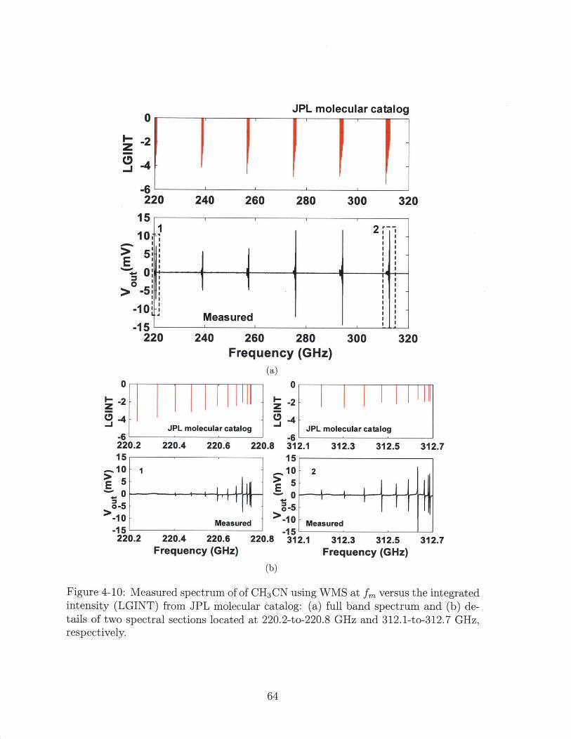
JPL molecular catalog
I I -
260 280 300
2 *~
I II II II II II I
_______ I I1 *t~I II II II II II IMeasuredI
I
260 280 300Frequency (GHz)
(a)
0
-2,
JPL molecular catalog J-6
0.2 220.4 220.6 220.8 312.1
0.2 220.4 220.6 220.8Frequency (GHz)
150-10
S-531
312.1
312.3 312.5 312
2 I I ]
Fir
.7
easured
312.3 312.5 312.7Frequency (GHz)
(b)
Figure 4-10: Measured spectrum of of CH3CN using WMS at fm versus the integratedintensity (LGINT) from JPL molecular catalog: (a) full band spectrum and (b) de-tails of two spectral sections located at 220.2-to-220.8 GHz and 312.1-to-312.7 GHz,respectively.
64
0
I-_z -2
-4
AR220 240 320
0
-10
-152 240
z0_j
320
0
-2
-4
-622
PL molecular catalog
15110
0
-1522
1L
Measured
I I Ir
15
10i
2to
III

SNR oc Pressure .
OCS
10 -- eCH3CN
10
101 100 101Pressure (Pa)
Figure 4-11: SNR,/, variation versus pressure degradation for the 279.685 GHz spec-tral line of OCS and the 294.251 GHz spectral line of acetonitrile (Av=78 Hz).
83 mV and the measured baseband RMS noise voltage Vui,, is 2.8 pV//'HI; as a
result, the output SNR,/, is 2.9x 10⁴ (or 89.2 dB) with 1 Hz bandwidth. We note that
this matches the theoretical calculation of 3.0 x 10⁴ very well, which further validates
our analysis in Section 2.1.
At the pressure of 10 Pa, the spectrum of another molecule, acetonitrile (CH 3CN),between 220 to 320 GHz with a period of 18.4 GHz is also measured and shown in
Fig. 4-10(a). Details of two spectral sections within 220.2-to-220.8 GHz and 312.1-
to-312.7 GHz are given in Fig. 4-10(b), which again agree with the JPL molecular
catalog [12]. The peak absorption coefficient for the 294.251-GHz spectral line (at
10 Pa) is 0.017 cm 1 . An output baseband SNR,/, of 7.4x 10³ is measured for 1 Hz
bandwidth. This is lower than the theoretical SNR derived from (2.11), mainly be-
cause the pressure-broadening effect for acetonitrile is more significant at 10 Pa, and
the frequency deviation that we used (Af =360 kHz) does not optimally match the
larger molecular linewidth (~2 MHz). As is seen next, such discrepancy does not
exist when the pressure is reduced below the Doppler-limited threshold.
Fig. 4-11 shows the change of SNR under the reduction of sample pressure (i.e.
molecule concentration) for the spectral line of OCS at 279.685 GHz and the spectral
line of acetonitrile at 294.251 GHz. As predicted in (2.11), the SNR,/, scales linearly
65
with the pressure when the pressure is sufficiently low. Based on the linear extrap-
olation, for OCS spectral line at 279.658 GHz, unity SNR under 1 Hz bandwidth
is associated with a sample pressure of 1.1 x 10⁻⁴ Pa. This means, for a gas sample
with 10-Pa pressure (i.e. no significant pressure broadening), an OCS concentration
of 1.1x10⁻⁵ or 11 ppm is detectable. Similarly, for spectral line of acetonitrile at
294.251 GHz, the sensitivity under the same condition is 1.4x 10- or 14 ppm. Ac-
cording to Table 2.1, if our setup is used to detect hydrogen cyanide (HCN), which has
-4xstronger absorption compared to OCS, the sensitivity should reach 3 ppm 2 . At
present, sample pre-concentration technology is widely adopted in gas sensing, which
can provide a concentration gain of 105. If our CMOS chipset is used in a setup with
such pre-concentration, a sensitivity at 10~',100-ppt level should be achievable.
Lastly, there is one possible error that the TX spurs shown in Fig. 4-3 probe the
spectral lines, which are then subsequently down-converted into IF band by mixing
with corresponding LO spurs in the RX. However, in simulation, the LO-power-
dependent mixer conversion loss is 84 dB, and the resultant inter-modulation com-
ponents in IF band are -100 dB lower than the actual IF signals. Thus, it is not a
limiting factor of the sensitivity. For validation, Fig. 4-12(a) presents the measured
spectrum of an OCS and CH3CN gas mixture. The pressure of the gas mixture is
10 Pascal. The volume ratio of the two gas samples is VoCs : VCH3CN ~1 : 60. To
further reduce the baseline ripple, WMS at 2 fm is performed. The measured spectra
(shown in Fig. 4-12(b) and Fig. 4-12(c)) are examined; no false spurs are observed
besides the superposed OCS and CH 3CN spectra.
2 This is not experimentally validated, because HCN is highly toxic.
66

260 280Frequency (GHz)
(a)I
S0.5
0
231.05Frequency (GHz)
8
6
E4
2
0
-2
.41-220.2 220.4 220.6
Frequency (GHz)
1
0.5
E
0
-0.5-231.1 316.1
(b)8
6
4E
>0
-21 .4 1
220.8 312.1
316.15Frequency (GHz)
CH 3CN 2
-4
312.3 312.5Frequency (GHz)
(c)
Figure 4-12: Measured spectrum of CH3CN and OCS gas mixture using WMS at(a) full band spectrum. (b) details of 231.061 GHz and 316.146 GHz spectralof OCS in the mixture. (c) details of 220.2-to-220.8 GHz and 312.1-to-312.7spectral lines of CH3CN in the mixture.
67
10
5E
0
0220
CH3CN 2CH 3CN I
OCS 1I-OCS 2
240 300
OCS I
320
OCS 2
A-
CH3CN I
w ri 1,~ i316.2
312.7
2fm :linesGHz
.
5
-o.5 L231

68
Chapter 5
Conclusions
A CMOS dual-frequency-comb spectrometer is presented in this thesis. A compar-
ison between this work and previous publications is given in Table 5.1. Through a
parallel spectral scanning using 20 comb lines, this spectrometer achieves more than
20 x speed enhancement and breaks the bandwidth-efficiency tradeoff in conventional
circuit design. A total radiated power of 5.2 mW and a 14.6-to-19.5 dB SSB NF are
obtained in measurements, which are not only the best among all silicon-based THz
electronics, but also even comparable with the performance of compound semiconduc-
tor devices (e.g. GaAs Schottky-barrier diode). The measured minimum detectable
absorption coefficient of this work is 7.2x 10⁻⁷ cm', which is higher than the prior
work in silicon, but still two orders lower than that reported in [13]. This is mainly
because of the lower on-chip antenna gain (10 dBi versus 25 dBi in [13] for TX and
RX). Such problem can be solved in the future by implementing multiple coherent
radiators for each comb channel (hence higher antenna gain).
In addition, fundamentals of frequency scanning spectrometer are discussed and
validated. The measured SNR matches the theoretical prediction. The Townes noise
due to square-law detection is the major limiting factor for sensitivity so far, which
leads to a linear dependency of SNR versus gas concentration. It is an interesting
issue to be addressed before we encounter shot noise. Based on the current silicon
semiconductor technology, the sensitivity of a fully-optimized spectrometer should
reach below 1-ppm level (or below 10-ppt with pre-concentration).
This technology is expected to be applied in future biomedical areas. The concen-
69

Table 5.1: Performance Comparison of Rotational SpectrometerMinimum
TX RX SSB DetectableSpectrometer Frequency Radiated Noise Path Absorption
Ref. Architec- Technology (GHz) Power Figure Length (cm-1) with(mW) (dB) 1-Hz
bandwidth
GaAs 2[11] Single-Tone Schottky 210-270 ~ ~14 1.2 2.7x 10⁻⁹
Barrier Diode
[14] Single-Tone 0.13ptm SiGe 238~252 5 18 1.9 4.3x10⁻⁶ 3BiCMOS
[16] Single-Tone 65nm CMOS 208~255 0.14 N/A 1 N/A
[19] Pulsed Echo 65nm CMOS 95-105 4 9.2 0.035 N/A
This Dual-
Work Frequency- 65nm CMOS 220~320 5.26 14.6~19.5 0.7 7.2x 10⁻⁷Comb
1 The radiated power and noise figure are estimated from performance of typical VDI instrument.2 agas,min~0.017 cm-'/(500x 1 s/O.01 sx 10 Pa/0.008 Pa)=2.7x 10- 9 cm-1 is calculated based on CH3 CN with pressure
of 6x10- 5 Torr (0.008 Pa). The reported SNR is 500 with 0.01 s integration time.3 agas,min~O0.0013 cm-1/300=4.3x 10- 6 cm- 1 is calculated based on 248.28 GHz spectral line of CH3 0H with pressure of
13 Pa. Its absorption coefficient is 0.0013 cm- 1 based on [53]. The measured SNR is 300 based on Fig.18 of [14]. Theintegration time hasn't been specified.
4 The reported power is EIRP, which includes the antenna gain of the chip.5 Effective path length is larger than physical length due to multi-reflection inside high Q semiconfocal cavity.6 Total radiated power of THz comb. The average radiated power is 0.5 mW for each comb line.
tration of volatile organic compounds (VOCs) in human exhaled breath ranges from
ppm to ppb level [1, 4], and the fluctuation of specified VOCs, normally at ppb level,
can be utilized as bio-markers for disease diagnosis. As shown in this work, sufficient
sensitivity is provided by silicon-based rotational spectrometers. This enables fast,
non-invasive monitoring/analysis of human health conditions.
70
Bibliography
[1] Frank K Tittel, Y Bakhirkin, A Kosterev, R Lewicki, S So, G Wysocki, andRF Curl. Recent advances and applications of mid-infrared based trace gassensor technology. In Integrated Optoelectronic Devices 2008, pages 69000Z-69000Z. International Society for Optics and Photonics, 2008.
[2] OK Varghese. Exhaled gas detection for medical diagnosis: Can it be made atool for self-screening. J Nanomed Res, 3(3):00056, 2016.
[3] Ivan R Medvedev, Robert Schueler, Jessica Thomas, 0 Kenneth, Hyun-Joo Nam,Navneet Sharma, Qian Zhong, David J Lary, and Philip Raskin. Analysis of ex-haled human breath via terahertz molecular spectroscopy. In Infrared, Millime-ter, and Terahertz waves (IRMMW-THz), 2016 41st International Conferenceon, pages 1-2. IEEE, 2016.
[4] Il-Doo Kim, Seon-Jin Choi, Sang-Joon Kim, and Ji-Su Jang. Exhaled breathsensors. In Smart Sensors for Health and Environment Monitoring, pages 19-49.Springer, 2015.
[5] Anton Amann, Wolfram Miekisch, Jochen Schubert, Boguslaw Buszewski,Tomasz Ligor, Tadeusz Jezierski, Joachim Pleil, and Terence Risby. Analysisof exhaled breath for disease detection. Annual Review of Analytical Chemistry,7:455-482, 2014.
[6] Helmut Giinzler and Hans-Ulrich Gremlich. Ir spectroscopy. an introduction.2002.
[7] Philip S Waggoner and Harold G Craighead. Micro-and nanomechanical sensorsfor environmental, chemical, and biological detection. Lab on a Chip, 7(10):1238-1255, 2007.
[8] Qing Wan, QH Li, YJ Chen, Ta-Hung Wang, XL He, JP Li, and CL Lin. Fabri-cation and ethanol sensing characteristics of zno nanowire gas sensors. AppliedPhysics Letters, 84(18):3654-3656, 2004.
[9] Wei Pang, Hongyuan Zhao, Eun Sok Kim, Hao Zhang, Hongyu Yu, and Xi-aotang Hu. Piezoelectric microelectromechanical resonant sensors for chemicaland biological detection. Lab on a Chip, 12(1):29-44, 2012.
71

[10] Charles H Townes and Arthur L Schawlow. Microwave spectroscopy. CourierCorporation, 2013.
[11] Ivan R Medvedev, Christopher F Neese, Grant M Plummer, and Frank C De Lu-cia. Submillimeter spectroscopy for chemical analysis with absolute specificity.Optics letters, 35(10):1533-1535, 2010.
[12] Jet Propulsion Laboratory. Molecular Spectroscopy Catalog.https://spec.jpl. nasa. gov/.
[13] Christopher F Neese, Ivan R Medvedev, Grant M Plummer, Aaron J Frank,Christopher D Ball, and Frank C De Lucia. Compact submillimeter/terahertzgas sensor with efficient gas collection, preconcentration, and ppt sensitivity.IEEE Sensors Journal, 12(8):2565-2574, 2012.
[14] Klaus Schmalz, Johannes Borngrdber, Wojciech Debski, Mohamed Elkhouly,Ruoyu Wang, Philipp F-X Neumaier, Dietmar Kissinger, and Heinz-WilhelmHiibers. 245-ghz transmitter array in sige bicmos for gas spectroscopy. IEEETransactions on Terahertz Science and Technology, 6(2):318-327, 2016.
[15] K. Schmalz, N. Rothbart, P. F. X. Neumaier, J. Borngr?ber, H. W. Hbers, andD. Kissinger. Gas spectroscopy system for breath analysis at mm-wave/thz usingsige bicmos circuits. IEEE Transactions on Microwave Theory and Techniques,65(5):1807-1818, May 2017.
[16] N Sharma, Q Zhong, Z Chen, W Choi, JP McMillan, CF Neese, R Schueler,I Medvedev, F De Lucia, et al. 200-280ghz cmos rf front-end of transmitter forrotational spectroscopy. In VLSI Technology, 2016 IEEE Symposium on, pages1-2. IEEE, 2016.
[17] D. J. Nemchick, B. J. Drouin, A. J. Tang, Y. Kim, and M. C. F. Chang. Sub-doppler spectroscopy with a cmos transmitter. IEEE Transactions on TerahertzScience and Technology, 8(1):121-126, Jan 2018.
[18] R. Han and E. Afshari. A cmos high-power broadband 260-ghz radiator arrayfor spectroscopy. IEEE Journal of Solid-State Circuits, 48(12):3090-3104, Dec2013.
[19] Adrian Tang, Brian Drouin, Yanghyo Kim, Gabriel Virbila, and Mau-Chung Frank Chang. 95 105 ghz 352 mw all-silicon cavity-coupled pulsed echorotational spectroscopy system in 65 nm cmos. IEEE Transactions on TerahertzScience and Technology, 2017.
[20] Y. D. Hsieh, Y. Iyonaga, Y. Sakaguchi, S. Yokoyama, H. Inaba, K. Minoshima,F. Hindle, Y. Takahashi, M. Yoshimura, Y. Mori, T. Araki, and T. Yasui. Ter-ahertz comb spectroscopy traceable to microwave frequency standard. IEEETransactions on Terahertz Science and Technology, 3(3):322-330, May 2013.
72

[21] C. Wang, B. Perkins, Z. Wang, and R. Han. Molecular detection for uncon-centrated gas with ppm sensitivity using 220-to-320-ghz dual-frequency-combspectrometer in cmos. IEEE Transactions on Biomedical Circuits and Systems,pages 1-13, 2018.
[22] Cheng Wang and Ruonan Han. Rapid and Energy-Efficient Molecular SensingUsing Dual mm-Wave Combs in 65nm CMOS: A 220-to-320GHz Spectrometerwith 5.2mW Radiated Power and 14.6-to-19.5dB Noise Figure. In InternationalSolid-State Circuit Conference (ISSCC), pages 18-20, San Francisco, CA, 2017.
[23] Cheng Wang and Ruonan Han. Towards Miniature Gas Sensor with High Speed,Wide Range and Absolute Specificity: A Bilateral Dual-Terahertz-Comb Spec-trometer on CMOS. submitted to IEEE Journal of Solid-State Circuits (JSSC),2017.
[24] James M Supplee, Edward A Whittaker, and Wilfried Lenth. Theoretical descrip-tion of frequency modulation and wavelength modulation spectroscopy. AppliedOptics, 33(27):6294-6302, 1994.
[25] J.W.M. Rogers, C. Plett, and F. Dai. Integrated Circuit Design for High-speedFrequency Synthesis. Artech House microwave library. Artech House, 2006.
[26] J. H. Van Vleck and V. F. Weisskopf. On the shape of collision-broadened lines.Reviews of Modern Physics, 17(2-3):227-236, 1945.
[27] J. Ko and R. Gharpurey. A pulsed uwb transceiver in 65 nm cmos with four-element beamforming for 1 gbps meter-range wpan applications. IEEE Journalof Solid-State Circuits, 51(5):1177-1187, May 2016.
[28] A. Medi and W. Namgoong. A high data-rate energy-efficient interference-tolerant fully integrated cmos frequency channelized uwb transceiver for impulseradio. IEEE Journal of Solid-State Circuits, 43(4):974-980, April 2008.
[29] Yi-Da Hsieh, Yuki Iyonaga, Yoshiyuki Sakaguchi, Shuko Yokoyama, Ha-jime Inaba, Kaoru Minoshima, Francis Hindle, Yoshinori Takahashi, MasashiYoshimura, Yusuke Mori, Tsutomu Araki, and Takeshi Yasui. Terahertz CombSpectroscopy Traceable to Microwave Frequency Standard. IEEE Transactionson Terahertz Science and Technology, 3(3):322-330, 2013.
[30] David Burghoff, Tsung-Yu Kao, Ningren Han, Chun Wang Ivan Chan, XiaoweiCai, Yang Yang, Darren J. Hayton, Jian-Rong Gao, John L. Reno, and Qing Hu.Terahertz Laser Frequency Combs. Nature Photonics, 8(6):462-467, 2014.
[31] Yi-Da Hsieh, Yuki Iyonaga, Yoshiyuki Sakaguchi, Shuko Yokoyama, Ha-jime Inaba, Kaoru Minoshima, Francis Hindle, Yoshinori Takahashi, MasashiYoshimura, Yusuke Mori, et al. Terahertz comb spectroscopy traceable to mi-crowave frequency standard. IEEE Transactions on Terahertz Science and Tech-nology, 3(3):322-330, 2013.
73

[32] David Burghoff, Tsung-Yu Kao, Ningren Han, Chun Wang Ivan Chan, XiaoweiCai, Yang Yang, Darren J Hayton, Jian-Rong Gao, John L Reno, and Qing Hu.Terahertz laser frequency combs. Nature Photonics, 8(6):462-467, 2014.
[33] Samuel Jameson, Eliezer Halpern, and Eran Socher. 20.4 a 300ghz wirelesslylocked 2 x 3 array radiating 5.4 dbm with 5.1% dc-to-rf efficiency in 65nm cmos.In Solid-State Circuits Conference (ISSCC), 2016 IEEE International, pages348-349. IEEE, 2016.
[34] Ruonan Han, Chen Jiang, Ali Mostajeran, Mohammad Emadi, HamidrezaAghasi, Hani Sherry, Andreia Cathelin, and Ehsan Afshari. 25.5 a 320ghz phase-locked transmitter with 3.3 mw radiated power and 22.5 dbm eirp for heterodynethz imaging systems. In Solid-State Circuits Conference-(ISSCC), 2015 IEEEInternational, pages 1-3. IEEE, 2015.
[35] Ullrich R Pfeiffer, Yan Zhao, Janusz Grzyb, Richard Al Hadi, Neelanjan Sarmah,Wolfgang Forster, Holger Rucker, and Bernd Heinemann. 14.5 a 0.53 thz recon-figurable source array with up to 1mw radiated power for terahertz imagingapplications in 0.13 pm sige bicmos. In Solid-State Circuits Conference Digestof Technical Papers (ISSCC), 2014 IEEE International, pages 256-257. IEEE,2014.
[36] X. D. Deng, Y. Li, J. Li, C. Liu, W. Wu, and Y. Z. Xiong. A 320-ghz ltimes4fully integrated phased array transmitter using 0.13-mum sige bicmos technol-ogy. IEEE Transactions on Terahertz Science and Technology, 5(6):930-940, Nov2015.
[37] Gang Liu, Jefy Jayamon, James Buckwalter, and Peter Asbeck. Frequency dou-blers with 10.2/5.2 dbm peak power at 100/202 ghz in 45nm soi cmos. In RadioFrequency Integrated Circuits Symposium (RFIC), 2015 IEEE, pages 271-274.IEEE, 2015.
[38] Hsin-Chang Lin and Gabriel M Rebeiz. A 200-245 ghz balanced frequency dou-bler with peak output power of+ 2 dbm. In Compound Semiconductor IntegratedCircuit Symposium (CSICS), 2013 IEEE, pages 1-4. IEEE, 2013.
[39] Berke Cetinoneri, Yusuf A Atesal, Andy Fung, and Gabriel M Rebeiz. W-bandamplifiers with 6-db noise figure and milliwatt-level 170-200-ghz doublers in 45-nm cmos. IEEE Transactions on Microwave Theory and Techniques, 60(3):692-701, 2012.
[40] Rouzbeh Kananizadeh and Omeed Momeni. 2.6 a 190.5 ghz mode-switching vcowith 20.7% continuous tuning range and maximum power of- 2.1 dbm in 0.13 pmbicmos. In Solid-State Circuits Conference (ISSCC), 2016 IEEE International,pages 46-47. IEEE, 2016.
[41] Navneet Sharma, Wooyeol Choi, and KO Kenneth. 160-310 ghz frequency dou-bler in 65-nm cmos with 3-dbm peak output power for rotational spectroscopy.
74

In Radio Frequency Integrated Circuits Symposium (RFIC), 2016 IEEE, pages186-189. IEEE, 2016.
[42] Taiyun Chi, Min-Yu Huang, Sensen Li, and Hua Wang. 17.7 a packaged 90-to-300ghz transmitter and 115-to-325ghz coherent receiver in cmos for full-bandcontinuous-wave mm-wave hyperspectral imaging. In Solid-State Circuits Con-ference (ISSCC), 2017 IEEE International, pages 304-305. IEEE, 2017.
[43] R. Han, C. Jiang, A. Mostajeran, M. Emadi, H. Aghasi, H. Sherry, A. Cathelin,and E. Afshari. A sige terahertz heterodyne imaging transmitter with 3.3 mwradiated power and fully-integrated phase-locked loop. IEEE Journal of Solid-State Circuits, 50(12):2935-2947, Dec 2015.
[44] Robert Spence. Linear Active Networks. John Wiley & Sons Ltd, 1970.
[45] Z. Wang and P. Heydari. A study of operating condition and design methodsto achieve the upper limit of power gain in amplifiers at near- fmax frequencies.IEEE Transactions on Circuits and Systems I: Regular Papers, 64(2):261-271,Feb 2017.
[46] H. Bameri and 0. Momeni. A high-gain mm-wave amplifier design: An ana-lytical approach to power gain boosting. IEEE Journal of Solid-State Circuits,52(2):357-370, Feb 2017.
[47] David Pozar. Microwave Engineering, Fourth Edition. Wiley, 2011.
[48] High-Frequency Structure Simulator User Guide. ANSYS Inc., 2014.
[49] K. Sengupta and A. Hajimiri. Distributed active radiation for thz signal genera-tion. In 2011 IEEE International Solid-State Circuits Conference, pages 288-289,Feb 2011.
[50] K.K. Clarke and D.T. Hess. Communication circuits: analysis and design.Addison-Wesley series in electrical engineering. Addison-Wesley Pub. Co., 1971.
[51] David B Rutledge, Dean P Neikirk, and Dayalan P Kasilingam. Integrated-circuit antennas. Infrared and millimeter waves, 10(part 2):1-90, 1983.
[52] Jacques Vanier and Laurent-Guy Bernier. On the signal-to-noise ratio and short-term stability of passive rubidium frequency standards. IEEE Transactions onInstrumentation and Measurement, 1001(4):277-282, 1981.
[53] Inc. GATS. Spectral Calculator. http://www.spectralcalc. com.
75