wide v dc/dc power solutions - texas instruments · · 2014-07-23wide v in dc/dc power solutions...
TRANSCRIPT

2014ti.com/widevin
Wide VIN DC/DC Power SolutionsFor Industrial, Automotive, and Communications Applications

Wide VIN DC/DC Power Solutions Texas Instruments 20142
Increased Power Density and Reliability For Applications Requiring Max Operating Voltages ≥30V
100V
75V
50V
40V
30VBuck Boost Buck-Boost Modules
Converter Controller Converter Controller Converter Controller
Max VIN
LinearRegulators
NexFETs
Texas Instruments provides the industry’s most comprehensive wide input voltage range DC/DC converter portfolio with rich feature sets to meet the demands of today’s high-performance systems. With operating voltages of up to 100V, TI’s Wide VIN portfolio eliminates input protection components to reduce cost and solution size. Extra margin is provided for robustness of un-characterized system conditions to increase system reliability. Additionally, a single device can operate across several voltage rails to provide scalability and allow reuse of power converter designs.
TI’s easy-to-use, high-density, feature-rich Wide VIN converters, controllers, and power modules reduce BOM size and cost while improving scalability and reliability without compromising performance.
Wide VIN DC/DC Portfolio
Wide VIN Capability System Benefit
Increased robustness against input transients Eliminates the need for external transient protection components, saves PCB area
Ability to convert high VIN to low VOUT Eliminates two-stage conversions, saves PCB area
High-power density modules Saves PCB area, simplifies design
Low noise, low EMI solutions Eliminates external filtering, improves quality of data signals
Stackable devices with current sharing Enables re-use across multiple applications
WEBENCH® design tools support Easy to design and optimize custom circuits
Wide VIN Power Benefits

Wide VIN DC/DC Power Solutions Texas Instruments 20143
Applications Requiring Wide VIN DC/DC ConversionDelivering High Performance Power Solutions for the Most Demanding Systems
Rugged Industrial Equipment•40V+WideVIN operation for 24V backplanes• IsolatedbiaspowerforPLCsandmotordrives• IntegratedFETbuckconvertersforreducing
PCB power footprint•Powermoduleswithintegratedinductorto
increase power density and reduce EMI•LownoiseLDOsforpoweringprecisioncircuits
Advanced Automotive Electronics•42V/60VWideVIN rating to survive load dump•>2MHzoperationtoreduceradiointerference•Lowstandby/shutdownIqtoreducebatterydrain•BuckcontrollersforinfotainmentandUSBpower•Boostsolutionswith3VminVIN for continuous operation
during start-stop events•Ultra-smallICpackagingtoreducePCBfootprint
Sensitive Communications Systems•75V/100VWideVIN operation for 48V backplanes•High-performancebuckcontrollersandMOSFETs
for powering high-current systems•LowEMIintegratedpowermodulesforreducingnoise
and PCB footprint•Constantfrequencyoperationformanagingpowersupplynoise•HighPSRRandlow-noiseregulatorsforpoweringRFcircuits

Wide VIN DC/DC Power Solutions Texas Instruments 20144
Wide VIN ConvertersIntegratedandEasy-to-UseforSpace-ConstrainedApplications
+
+
+
+
VINBST
RON
RTN
SW
VCC
FBUVLO
VIN
VOUT1
VOUT2
R FB 1RUV 1
RON
COUT 1
CBST
D1
CIN
C OUT 2
R FB2
RUV 2
X1
Rr
N P
N SLM5017
CVCC+
D2
9V-100V
Wide VIN Converters
DeviceOutput
Current (A)Input Voltage
Range (V)Output Voltage
Range (V)Frequency Range (kHz) and Sync Synchronous AECQ
PWM Mode
Buck Converters
TPS54062/1 0.05/0.2 4.7 to 60 0.8 to 58 50 to 1100, Sync 4 – / 4 CM
LM(2)5017/8/9* 0.6/0.3/0.1 9 to 48/100 1.25 to 40/90 50 to 1000 4 — COT
LM5008A/9A 0.35/0.15 6 to 95 2.5 to 85 50 to 600 — — COT
LMR14203/6 0.3/0.6 4.5 to 42 0.765 to 34 1250 — — CM
LM(2)5574/5/6* 0.5/1.5/3 6 to 42/75 1.23 to 70 50 to 1000 — 4 ECM
LM22674/75/80 0.05/1/2 4.5 to 42 1.285 to 37 200 to 1000 — 4 VM
LM(2)5007* 0.5 9 to 75 2.5 to 37/73 50 to 800 — — COT
LM34919C 0.6 4.5 to 50 2.5 to 45 up to 2600 — 4 COT
LM5006 0.65 6 to 75 2.5 to 75 50 to 800 4 — COT
LM(2)5010A* 1 6 to 42/75 2.5 to 37/70 50 to 1000 — 4 COT
LMR24210/20 1/2 4.5 to 42 0.8 to 24 1000 max 4 — COT
TPS54140/60 A 1.5 3.5 to 42/60 0.8 to 40/58 100 to 2500, Sync — 4 CM
LM25011 2 6 to 42 2.5 to 40 up to 2000 — 4 COT
LM(2)5005* 2.5 7 to 42/75 1.23 to 37/70 50 to 500, Sync — — ECM
TPS54240/60 2.5 3.5 to 42/60 0.8 to 40/58 100 to 2500, Sync — 4 CM
LM43602/03 2/3 3.5 to 36 1.0 to 28 200 to 2200, Sync 4 4 / — CM
TPS54340/60 3.5 4.5 to 42/60 0.8 to 58.8 100 to 2500, Sync — 4 CM
LM22677/8/9 5 4.5 to 42 1.285 to 37 200 to 1000 — 4 VM
TPS54540/60 5 4.5 to 42/60 0.8 to 58.8 100 to 2500, Sync — 4 CM
Boost Converters
TPS55332 0.5 3.6 to 60 2.5 to 50 80 to 2200, Sync — 4 VM
LM5000/1/2 2/1/0.5 3.1 to 40/75 1.26 to 75 up to 1500 — — CM
Buck-Boost Converters
TPS55065 0.5 1.5 to 40 5 440 — 4 VM
* (2) indicates a lower voltage option, check data sheet for input voltage range
LM5017 Family of 100V Regulators Enhance Reliability for High-Voltage Systems•Wide9–100Voperatinginputrangeprovidesimprovedtransientprotection• Integrated100VFETsreduceexternalcomponentsandBOMcost•COTarchitecturerequiresnoloopcompensation,reducingsolutionsize•Alsofeaturesintelligentpeakcurrentlimit,adjustableUVLO,andthermalshutdown

Wide VIN DC/DC Power Solutions Texas Instruments 20145
Wide VIN ControllersHigh-Performance for High-Current Power Conversion Needs
Wide VIN Controllers
DeviceInput Voltage
Range (V)# of
OutputsOutput Min (V)
Output Max Voltage (V)
Frequency Range (kHz) and Sync Synchronous AECQ
PWM Mode
Buck Controllers
LM3150/1/2 6 to 42 1 0.6/3.3/3.3 40/3.3/3.3 200 to 1000/250/500 4 — COT
TPS40170 4.5 to 60 1 0.6 57 100 to 600, Sync 4 4 VFF
LM(2)5117* 5.5 to 65 1 0.8 58 50 to 750, Sync 4 4 ECM
LM(2)5119* 5.5 to 65 2 0.8 58 50 to 750, Sync 4 4 ECM
TPS43340 4 to 40 4 0.9 11 150 to 600, Sync 4 4 CM
TPS43350/1 4 to 40 2 0.9 11 150 to 600, Sync 4 4 CM
LM(2)5116* 6 to 100 1 1.215 80 50 to 1000, Sync 4 — ECM
LM(2)5085/8* 4.5 to 75 1 1.25/1.2 75/70 50 to 1000 — 4 COT/ECM
Boost Controllers
LM5022 6 to 60 1 1.25 † up to 1000, Sync — — CM
LM3478/88 2.95 to 40 1 1.26 † 100 to 1000, Sync — 4 CM
LM3481 2.97 to 48 1 1.275 † 100 to 1000, Sync — 4 CM
LM5121/2 3 to 65 1 3 100 up to 1000, Sync 4 4 CM
TPS43060/1 4.5 to 40 1 4.5 60 50 to 1000, Sync 4 – CM
TPS40210 4.5 to 52 1 5 † 50 to 1000, Sync 4 4 CM
Buck-Boost and Buck + Boost Controllers
LM(2)5118* 3 to 75 1 1.23 70 50 to 500, Sync — 4 ECM
TPS43330 4 to 40 3 0.09 11 150 to 600, Sync 4 4 CM
* (2) indicates a lower voltage option, check data sheet for input voltage range † Maximum output voltage is set by external feedback resistors
LM5121/22 Family of Stackable, Wide VIN Syncronous Boost Controllers•Wideinput/outputrangeaccommodatesautomotivecoldcrankandloaddump•3–65VIN and up to 100 VOUT
•LM5122Multi-phasecapabilityforhigh-powerIndustrial,Automotive,andTelecom•LM5121Disconnectswitchenablesfaultprotectionandcompleteloaddisconnect
VCC
LM5121/22
CSN
DG
SYNCIN/RT
RES
SSUVLO
VIN
AGND
BST
MODE
PGNDSLOPE
COMP
FB
HO
LO
SW
+
DS
VOUTVIN
CSP
OPTSYNCOUT
LM5121: Pins for Disconnect Switch Control
LM5122: Pins for Multi-Phase Con�guration

Enable
CIN
40 µF
CSS0.47 µF
RFBBSee Table
See Table
440 µF
VOUT at 10A
CFF 180 pF (OPT)
RFBT
LMZ23610
VIN VIN
EN AGND
PGND
FB SS VOUT
Wide VIN DC/DC Power Solutions Texas Instruments 20146
Wide VIN Power ModulesForLow-NoiseDesignsthatRequireanExtremelyFastTimetoMarket
Wide VIN SIMPLE SWITCHER® Modules
DeviceOutput
Current (A)Input Voltage
Range (V) # of OutputsOutput Voltage
Range (V)Frequency Range
(kHz) & SyncCurrent Sharing
Buck Modules
LMZ14201/H 1 6 to 42 1 0.8 to 6/5 to 24 adj to 1000
LMZ14202/H 2 6 to 42 1 0.8 to 6/5 to 24 adj to 1000
LMZ35003 2.5 7 to 50 1 2.5 to 15 400 to 1000
LMZ14203/H 3 6 to 42 1 0.8 to 6/5 to 24 adj to 1000
LMZ23603/5 3/5 6 to 36 1 0.8 to 6 650 to 950, Sync
LMZ13608/10 8/10 6 to 36 1 0.6 to 6 360
LMZ23608/10 8/10 6 to 36 1 0.6 to 6 315 to 600, Sync 4
Inverting Modules
LMZ34002 2 4.5 to 40 1 -3 to -17 500 to 800
* Modules available for extended temperature operation to -55°C
VOUTVIN
LMZ35003
VADJ
AGND PGND
V OUTV IN
INH/UVLO
STSEL
C IN R SETC OUT
LMZ35003 2.5A SIMPLE SWITCHER® Power Module in Low Profile QFN Package•Wideinputvoltagerangefrom7Vto50V (65Vsurgecapability)
•Outputadjustablefrom2.5Vto15V•Efficiencyupto96%•LowEMI:meetsEN55022classB
LMZ23610 10A SIMPLE SWITCHER Power Module in Easy-to-Use PFM Package•Wideinputvoltagerangefrom6Vto36V•Outputadjustablefrom0.8Vto6V•Singleexposedpadandstandardpinoutforeasymountingandmanufacturing•LowEMI:meetsEN55022classB

Wide VIN DC/DC Power Solutions Texas Instruments 20147
Wide VIN NexFET™ Power MOSFETsOptimizedforDC/DCPowerConversionwithLowRDSON and Gate Charge•60Vand100VNexFETpairsprovidebest-in-classperformanceforDC/DCconversionneeds
Wide VIN Linear RegulatorsDeliveringLowNoiseandFastTransientResponseforSensitiveApplications
TPS709xx Family: 30V, 150 mA Ultralow Iq LDO with Reverse Current Protection and enable•Wide2.7Vto30Vinputvoltagerange•Outputcurrentupto150mA•Ultra-lowIq:1.35µA•Lowdropout:245mVat50mAload
Wide VIN NexFETs
Device BVSS (V) Vgs (V)RDS(ON) typ
10V (mW)ID at 25°C
(A)Qg at 10V Typ (nC)
Qgd Typ (nC)
Qgs Typ (nC)
Qrr 300A/µs Typ (nC)
CSD18501Q5A 40 20 3 155 42 6 8 70
CSD18502Q5B 40 20 2 204 25 8 10 88
CSD18537NQ5A1 60 20 10 62 14 2 5 54
CSD18563Q5A1 60 20 6 98 29 5 7 57
CSD19502Q5B 80 20 3 138 48 9 14 275
CSD19532Q5B 100 20 4 124 48 9 13 249
CSD19534Q5A2 100 20 13 137 17 3 5 134
CSD19533Q5A2 100 20 8 100 27 5 8 1631 2 Recommended high-side and low-side pairs
For more Wide VIN NexFET™ products, visit ti.com/nexfet
Wide VIN Linear Regulators
DeviceOutput
Current (A)Input Voltage
Range (V)Output Voltage
Range (V)Dropout (mV) at Max Load
PSRR at 100kHz (dB)
Output Noise (µVrms) Key Features
TPS7A40 0.05 7 to 100 1.1 to 90 780 65 dB at 100 Hz * Fast transient response
LM2936HV 0.05 5.5 to 60 3 to 5 200 60 dB at 120 Hz † Reverse voltage protection
LM9036 0.05 3.3 to 40 3.3 to 5 200 60 dB at 120 Hz * Reverse voltage protection
TPS7A16 0.1 3 to 60 1.2 to 18.5 265 50 dB at 100 Hz † 5µA Iq, Power Good
LM9076 0.15 3.3 to 40 3.3 to 5 150 60 dB at 120 Hz * Integrated reset
TPS709 0.15 2.7 to 30 1.2 to 5 460 52 dB at 1kHz † 1.35 µA Iq
TPS7A49 0.15 3 to 36 1.2 to 33 333 53 dB 12.7 µVrms Low noise, high PSRR
TPS7A30 0.2 -3 to -36 -1.18 to -33 325 55 dB 14 µVrms Low noise, high PSRR
TPS7A47 1 3 to 36 1.4 to 34 307 60 dB 4 µVrms Low noise, high PSRR
TPS7A33 1 -3 to -36 -1.2 to -33 307 64 dB 16 µVrms Low noise, high PSRR
* Output noise not specified, see datasheet for more details† Refer to datasheet for output noise at different frequencies
IN
GND
EN
OUT
NC
TPS709xx
VIN
1 µF 2.2 µF
VOUT
TPS709xx
SLPT040
SIMPLESWITCHERandWEBENCHareregisteredtrademarksandtheplatformbarisatrademarks
of Texas Instruments. All other trademarks are the property of their respective owners.
© 2014 Texas Instruments IncorporatedPrintedintheU.S.A.AlmadenPress, San Jose, CA
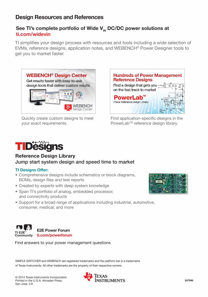
Design Resources and References
See TI’s complete portfolio of Wide VIN DC/DC power solutions at ti.com/widevin
TIsimplifiesyourdesignprocesswithresourcesandtoolsincludingawideselectionofEVMs, reference designs, application notes, and WEBENCH® Power Designer tools to get you to market faster.
Reference Design LibraryJump start system design and speed time to market
TI Designs Offer:•Comprehensivedesignsincludeschematicsorblockdiagrams, BOMs,designfilesandtestreports
•Createdbyexpertswithdeepsystemknowledge•SpanTI’sportfolioofanalog,embeddedprocessor,
and connectivity products•Supportforabroadrangeofapplicationsincludingindustrial,automotive,
consumer, medical, and more
TM E2E Power Forumti.com/powerforum
Find answers to your power management questions
Quickly create custom designs to meet your exact requirements.
Findapplication-specificdesignsinthePowerLabTM reference design library.

IMPORTANT NOTICETexas Instruments Incorporated and its subsidiaries (TI) reserve the right to make corrections, enhancements, improvements and otherchanges to its semiconductor products and services per JESD46, latest issue, and to discontinue any product or service per JESD48, latestissue. Buyers should obtain the latest relevant information before placing orders and should verify that such information is current andcomplete. All semiconductor products (also referred to herein as “components”) are sold subject to TI’s terms and conditions of salesupplied at the time of order acknowledgment.TI warrants performance of its components to the specifications applicable at the time of sale, in accordance with the warranty in TI’s termsand conditions of sale of semiconductor products. Testing and other quality control techniques are used to the extent TI deems necessaryto support this warranty. Except where mandated by applicable law, testing of all parameters of each component is not necessarilyperformed.TI assumes no liability for applications assistance or the design of Buyers’ products. Buyers are responsible for their products andapplications using TI components. To minimize the risks associated with Buyers’ products and applications, Buyers should provideadequate design and operating safeguards.TI does not warrant or represent that any license, either express or implied, is granted under any patent right, copyright, mask work right, orother intellectual property right relating to any combination, machine, or process in which TI components or services are used. Informationpublished by TI regarding third-party products or services does not constitute a license to use such products or services or a warranty orendorsement thereof. Use of such information may require a license from a third party under the patents or other intellectual property of thethird party, or a license from TI under the patents or other intellectual property of TI.Reproduction of significant portions of TI information in TI data books or data sheets is permissible only if reproduction is without alterationand is accompanied by all associated warranties, conditions, limitations, and notices. TI is not responsible or liable for such altereddocumentation. Information of third parties may be subject to additional restrictions.Resale of TI components or services with statements different from or beyond the parameters stated by TI for that component or servicevoids all express and any implied warranties for the associated TI component or service and is an unfair and deceptive business practice.TI is not responsible or liable for any such statements.Buyer acknowledges and agrees that it is solely responsible for compliance with all legal, regulatory and safety-related requirementsconcerning its products, and any use of TI components in its applications, notwithstanding any applications-related information or supportthat may be provided by TI. Buyer represents and agrees that it has all the necessary expertise to create and implement safeguards whichanticipate dangerous consequences of failures, monitor failures and their consequences, lessen the likelihood of failures that might causeharm and take appropriate remedial actions. Buyer will fully indemnify TI and its representatives against any damages arising out of the useof any TI components in safety-critical applications.In some cases, TI components may be promoted specifically to facilitate safety-related applications. With such components, TI’s goal is tohelp enable customers to design and create their own end-product solutions that meet applicable functional safety standards andrequirements. Nonetheless, such components are subject to these terms.No TI components are authorized for use in FDA Class III (or similar life-critical medical equipment) unless authorized officers of the partieshave executed a special agreement specifically governing such use.Only those TI components which TI has specifically designated as military grade or “enhanced plastic” are designed and intended for use inmilitary/aerospace applications or environments. Buyer acknowledges and agrees that any military or aerospace use of TI componentswhich have not been so designated is solely at the Buyer's risk, and that Buyer is solely responsible for compliance with all legal andregulatory requirements in connection with such use.TI has specifically designated certain components as meeting ISO/TS16949 requirements, mainly for automotive use. In any case of use ofnon-designated products, TI will not be responsible for any failure to meet ISO/TS16949.Products ApplicationsAudio www.ti.com/audio Automotive and Transportation www.ti.com/automotiveAmplifiers amplifier.ti.com Communications and Telecom www.ti.com/communicationsData Converters dataconverter.ti.com Computers and Peripherals www.ti.com/computersDLP® Products www.dlp.com Consumer Electronics www.ti.com/consumer-appsDSP dsp.ti.com Energy and Lighting www.ti.com/energyClocks and Timers www.ti.com/clocks Industrial www.ti.com/industrialInterface interface.ti.com Medical www.ti.com/medicalLogic logic.ti.com Security www.ti.com/securityPower Mgmt power.ti.com Space, Avionics and Defense www.ti.com/space-avionics-defenseMicrocontrollers microcontroller.ti.com Video and Imaging www.ti.com/videoRFID www.ti-rfid.comOMAP Applications Processors www.ti.com/omap TI E2E Community e2e.ti.comWireless Connectivity www.ti.com/wirelessconnectivity
Mailing Address: Texas Instruments, Post Office Box 655303, Dallas, Texas 75265Copyright © 2014, Texas Instruments Incorporated