who is at&s? - · pdf fileims printed circuit boards ... • hidden electronics...
TRANSCRIPT

Santa Clara Valley Chapter, Components, Packaging and Manufacturing Technology Society
July 23, 2015
www.cpmt.org/scv/ 1
Embedding Passive and Active Devices in Substrates
Michael Tschandl
AT & S Austria Technologie & Systemtechnik Aktiengesellschaft | Fabriksgasse13 | A-8700 Leoben Tel +43 (0) 3842 200-0 | E-Mail [email protected]
www.ats.net
IEEE/CPMT Santa Clara ValleyJuly 23, 2015
Who is AT&S?
Austria based global technology group focused on High Density Interconnect (HDI) Printed Circuit Boards, Advanced Packaging and IC Substrates.
AT&S commercializes leading-edge technology for the mobile devices, automotive & aviation, industrial electronics, medical & healthcare and advanced packaging sectors.
AT&S offers Embedded Component Packaging (ECP®) as a patent protected packaging solution. ECP® embeds active or passive components inside a PCB or IC Package
1
IC Package.
AT&S has 6 manufacturing sites in Austria (2), China (2), India, and South Korea.
Santa Clara Valley Chapter, Components, Packaging and Manufacturing Technology Society
July 23, 2015
www.cpmt.org/scv/ 2
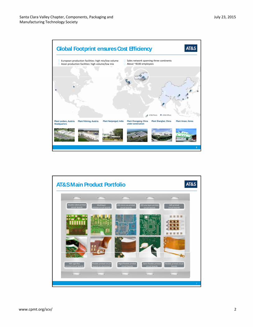
Global Footprint ensures Cost Efficiency
European production facilities: high mix/low volumeAsian production facilities: high volume/low mix
Sales network spanning three continentsAbout ~8100 employees
2
Plant Shanghai, China Plant Ansan, KoreaPlant Nanjangud, India Plant Chongqing, China under construction
Plant Leoben, AustriaHeadquarters
Plant Fehring, Austria
AT&S OfficesAT&S Plants
HDI micro via printed circuit boards
HDI any-layer printed circuit boards
IMS printed circuit boards
Multilayer printed circuit boards
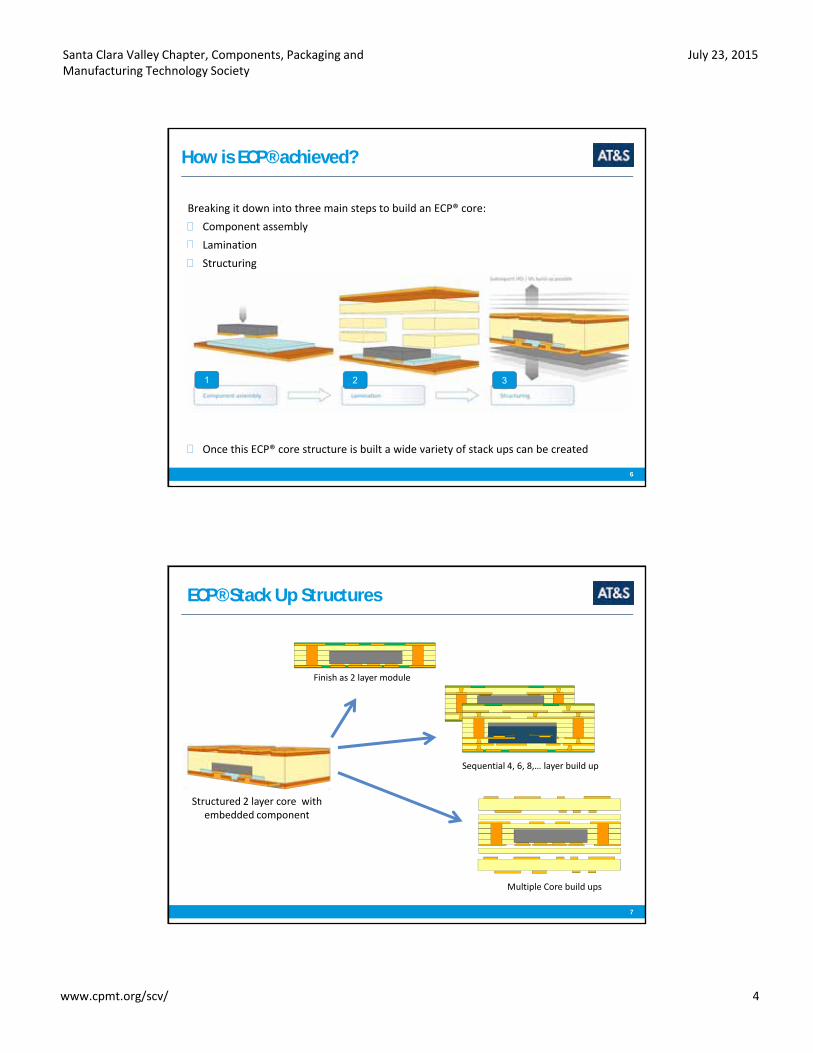
AT&S Main Product Portfolio
Double-sided printed circuit boards
3
Flexible printed circuit boards
Semi-flexible printed circuit boards
Rigid-flexible printed circuit boards
Flexible printed circuit boards on aluminium
HDI rigid-flex printed circuit boards

Santa Clara Valley Chapter, Components, Packaging and Manufacturing Technology Society
July 23, 2015
www.cpmt.org/scv/ 3
What is ECP®?
ECP® (Embedded Component Packaging) is patent protected packaging solution.
ECP® offers miniaturization, performance and reliability benefits.
ECP® uses the space inside an organic, laminate substrate (Printed Circuit Board) to embed active and/or passive components.
Components will be integrated in the core of the substrate and connected by
4
copper plated micro vias.
Basic Process and Architecture
5
Santa Clara Valley Chapter, Components, Packaging and Manufacturing Technology Society
July 23, 2015
www.cpmt.org/scv/ 4
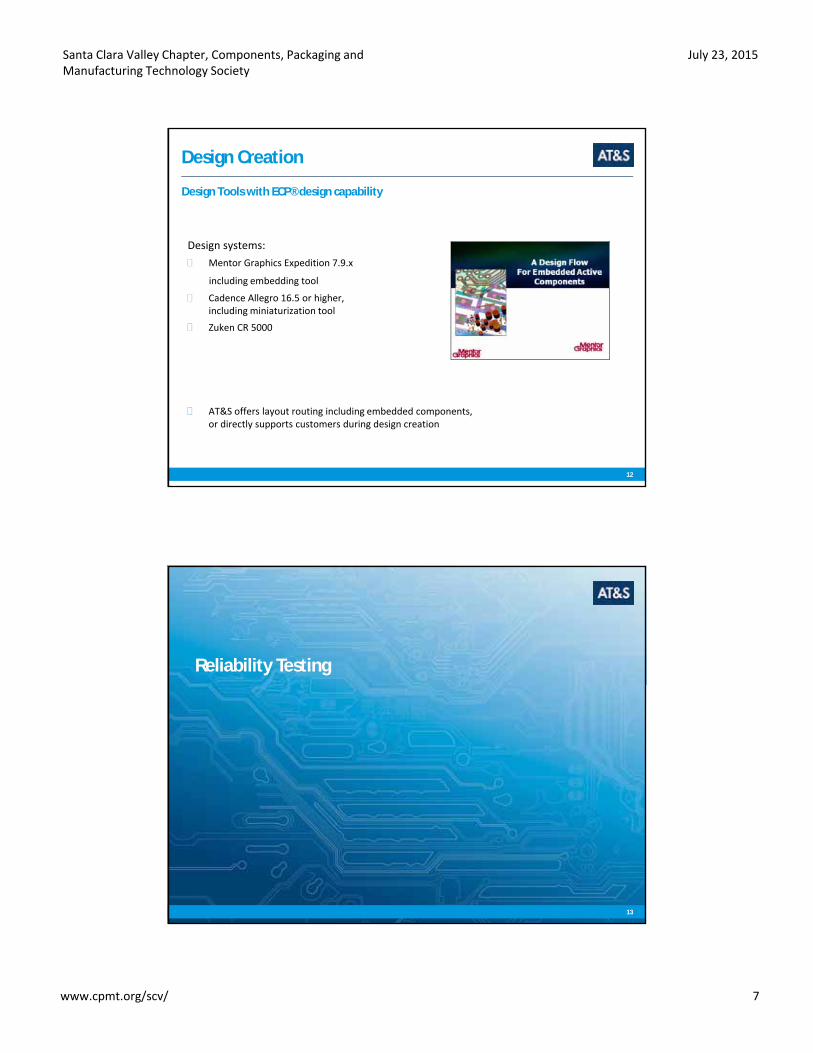
How is ECP® achieved?
Breaking it down into three main steps to build an ECP® core:
Component assembly
LaminationLamination
Structuring
6
Once this ECP® core structure is built a wide variety of stack ups can be created
1 2 3
ECP® Stack Up Structures
Finish as 2 layer module
Structured 2 layer core with
Sequential 4, 6, 8,… layer build up
7
Structured layer core withembedded component
Multiple Core build ups

Santa Clara Valley Chapter, Components, Packaging and Manufacturing Technology Society
July 23, 2015
www.cpmt.org/scv/ 5
ECP® Cross Sections
X-section of embedded components
Surface mount CSP
Substrate with embedded IC
8
Why ECP®?
Advantages
Miniaturization• Footprint reduction, z-height reduction• Higher component integration (additional assembly layer 3 vs 2)
Electrical Performance• Improved signal integrity
Electrical Performance • Reduction of parasitic influence (higher data rates)
Mechanical Performance
• Higher durability and reliability through copper-to-copper connections (with copper filled micro vias)
• Package functions as protective enclosure• High drop, shock and vibration tolerance
Thermal Management• Improved heat dissipation through direct copper connection• Improved heat dissipation FR4 versus air (compared to SMD)
Additional functions Reduction of overall cost
EMV Shi ldi
• EMV shielding (partial or full shielding of a package)• Package is the housing no additional molding required
9
EMV Shielding
Supporting the trend toward modularization
• Lower set-up costs compared to other packaging technologies (packaging versus substrate processes)
• Customization of module variants accomplished with digital imaging – no expensive tooling necessary (e.g. QFN,…)
Anti-Tamper / Security• Hidden electronics preventing reverse engineering and
counterfeiting

Santa Clara Valley Chapter, Components, Packaging and Manufacturing Technology Society
July 23, 2015
www.cpmt.org/scv/ 6
ECP® Component Basic Requirements
Pad finish: Cu plating needed for contacting
with micro vias = existing process for WLP
components
Use of thin components with copper terminations
Passive - discrete embeddablesWafer based embeddables
components
Pad pitch: adaptation to organic substrate
design rule through RDL
Wafer thinning: 100-150µm (recommended
thickness)
Capacitors and resistors available
Other discrete components in development
Component thickness 100µm – 330µm
Case sizes 0201, 0402
Components are connected by using
copper plated micro vias
RDL…redistribution layer
WLP…Wafer Level Package
10
What is needed for an ECP® project?
AT&S works with the leading passive componentComponents
Design
AT&S works with the leading passive component suppliers and semiconductor companies and can provide support or take over component sourcing
AT&S offers layout routing including embedded components, or directly supports customers during design creation
Embedding in Substrate
AT&S has years of experience in production of PCBs and packages with embedded components and can combine embedding with different package stack up technologies
11
Santa Clara Valley Chapter, Components, Packaging and Manufacturing Technology Society
July 23, 2015
www.cpmt.org/scv/ 7
Design Creation
Design Tools with ECP® design capability
Design systems:Design systems:
Mentor Graphics Expedition 7.9.x
including embedding tool
Cadence Allegro 16.5 or higher, including miniaturization tool
Zuken CR 5000
12
AT&S offers layout routing including embedded components, or directly supports customers during design creation
Reliability Testing
13
Santa Clara Valley Chapter, Components, Packaging and Manufacturing Technology Society
July 23, 2015
www.cpmt.org/scv/ 8
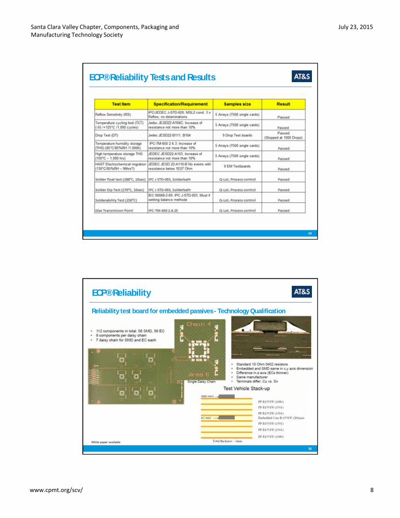
ECP® Reliability Tests and Results
14
ECP® Reliability
Reliability test board for embedded passives - Technology Qualification
White paper available
15
Santa Clara Valley Chapter, Components, Packaging and Manufacturing Technology Society
July 23, 2015
www.cpmt.org/scv/ 9
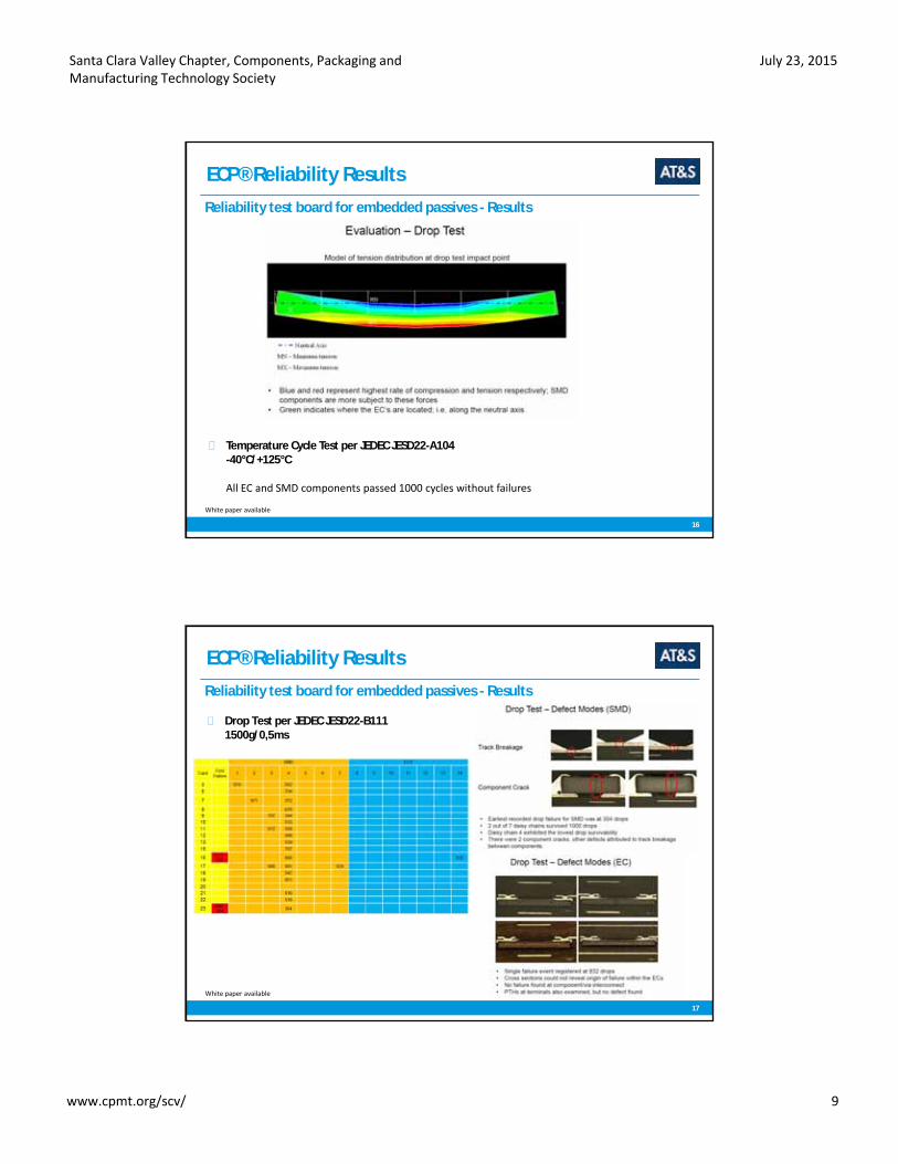
ECP® Reliability Results
Reliability test board for embedded passives - Results
White paper available
Temperature Cycle Test per JEDEC JESD22-A104 -40°C/+125°C
All EC and SMD components passed 1000 cycles without failures
16
ECP® Reliability Results
Reliability test board for embedded passives - Results
Drop Test per JEDEC JESD22-B111 1500g/0,5ms
White paper available
17

Santa Clara Valley Chapter, Components, Packaging and Manufacturing Technology Society
July 23, 2015
www.cpmt.org/scv/ 10
ECP® Reliability
Reliability test board for embedded actives – Technology Qualification
White paper available 7x7 pin Daisy Chain component with copper RDL
18
ECP® Reliability Results
Reliability test board for embedded actives - Results
Drop Test per JEDEC JESD22-B1111500g/0,5ms
White paper available
19

Santa Clara Valley Chapter, Components, Packaging and Manufacturing Technology Society
July 23, 2015
www.cpmt.org/scv/ 11
ECP® Reliability Results
Reliability test board for embedded actives – Results
Temperature Cycle Test per JEDEC JESD22-A104 -40°C/+125°C
Failure modes
White paper available
20
Application Examples
21

Santa Clara Valley Chapter, Components, Packaging and Manufacturing Technology Society
July 23, 2015
www.cpmt.org/scv/ 12
Trends in the Electronics Industry - Module / Packages
Module / Packages
Integration of Electronics in our daily lives - Technology meets Design
Integra on of new features in devices (Example: Sensors) – smallest packages and highest performance –ECP Technology opens up new possibilities
22
3D X-Ray Picture of a Module with Embedded Components
Picture: AT&S
Flexibility due to modular design
Where ECP® is being usedTightly spaced electronic devices
Modular design to shorten time-to-market
Trends in the Electronics Industry - Module / Packages
Smartwatches
Activity Trackers
Heart rate monitors / pulse oximeters
Sensors
Modular design to shorten time to market cycles
5.5mm x 3.9mm x 1.2mm
23
Picture: AT&S
Optical Heart Rate Monitoring System with 1 embedded IC controller

Santa Clara Valley Chapter, Components, Packaging and Manufacturing Technology Society
July 23, 2015
www.cpmt.org/scv/ 13
Trends in the Electronics Industry - Module / Packages
Flexibility due to modular design
Where ECP® is being used
Customers require design flexibility
Increasing density requires higher complexity of the circuit board Connectivity modules
(M2M communication)
Power Modules
Interface Modules
Control units
the circuit board
Adoptions in design cause time- and cost intensive approval processes
2.3mm x 2.9mm x 1.0mm
24
Picture: AT&S Engine Control Module: 416 I/O Processor embedded
DC/DC Converter with embedded active
Trends in the Electronics Industry - Power Modules
Steadily increasing demands for Power Management
Every operational unit has to have a power supply
Smaller energy sources require more efficient use gy qof available capacity
Thermal Management Where ECP® is being used
Battery Management
Power Modules
Power MOSFETs
25
Picture: AT&S
Power Module: 4 MOSFETs embedded

Santa Clara Valley Chapter, Components, Packaging and Manufacturing Technology Society
July 23, 2015
www.cpmt.org/scv/ 14
Trends in the Electronics Industry - GaN / SiC
Market for advanced power modules
Automotive
Infrastructure
Industrial
Technology shift coming – move to high efficiency semiconductor – GaN / SiC
Packaging = Significant Value-Add
26
Further Application Examples
µP
Processor
Active shielding - complete Active shielding - partial Data protection
µP
Fingerprint sensor
Memory
27
3D IntegrationUser authentication
Authentication 2.5DC Cavity integration
Memory
Fingerprint sensor Memory
Power Transistor

Santa Clara Valley Chapter, Components, Packaging and Manufacturing Technology Society
July 23, 2015
www.cpmt.org/scv/ 15
Standardization
System-in-Package
− ECP as Package
− Standard qualification process
• AEC Q100, JESD-22, MIL-STD-883…, ,
System-in-Board
− ECP as Substrate
− No standard in place yet
− AT&S working with IPC Committee
Embedding-specific standard (IPC-7092)
28
We are developing our ECP® technology further in terms of
Embedded die size (beyond 10 x 10 mm)
E b dd d di thi k (l th 100 )
Further development of ECP®
Technology Outlook
Embedded die thickness (less than 100µm)
Embedded passive component thickness (01005, 0201, 0402, 0803,…)
Wider height combination range for embedded components (active and passive)
Material selection (wider variety of Cu foils and prepregs)
Flexibility of build up concepts
Source: Fraunhofer IZM

Santa Clara Valley Chapter, Components, Packaging and Manufacturing Technology Society
July 23, 2015
www.cpmt.org/scv/ 16
AT&S ECP® Technology
Summary
Key benefits of ECP®
Miniaturization
Improved Electrical Performance
Improved Mechanical Performance
Enhanced Thermal Management
Embedded component / no additional housing required
Security / Anti-tamper
Shielding
30
ECP® has been in volume production at AT&S for several years (>200 Mio units in the field today)
ECP® can be combined with various substrate buildups
We can support product development, production and even take over part of the
supply chain, if required
We possess the necessary IP Portfolio for supporting your projects
AT&S – first choice for advanced applications
Michael Tschandl
VP / Head of Sales BU Advanced Packaging
AT&S Americas LLC1735 N. 1st Street, Ste 245San Jose, CA 95112USA
h dl
Visit www.ats.net
31
T: +1 408-573-1201C: +1 408-334-0508