wei-shun chang et al- low absorption losses of strongly coupled surface plasmons in nanoparticle...
TRANSCRIPT

8/3/2019 Wei-Shun Chang et al- Low absorption losses of strongly coupled surface plasmons in nanoparticle assemblies
http://slidepdf.com/reader/full/wei-shun-chang-et-al-low-absorption-losses-of-strongly-coupled-surface-plasmons 1/26
Low absorption losses of strongly coupled surfaceplasmons in nanoparticle assembliesWei-Shun Changa, Britain A. Willinghama, Liane S. Slaughtera, Bishnu P. Khanala, Leonid Vigdermana,Eugene R. Zubareva, and Stephan Linka,b,1
aDepartment of Chemistry, and bDepartment of Electrical and Computer Engineering, Laboratory for Nanophotonics, Rice University, Houston, TX 77005
Edited by Federico Capasso, Harvard University, Cambridge, MA, and approved September 26, 2011 (received for review August 20, 2011)
Coupled surface plasmons in one-dimensional assemblies of metal
nanoparticles have attracted significant attention because strong
interparticle interactions lead to large electromagnetic field
enhancements that can be exploited for localizing and amplifying
electromagnetic radiation in nanoscale structures. Ohmic loss (i.e.,
absorption by the metal), however, limits the performance of any
application due to nonradiative surface plasmon relaxation. While
absorption losses have been studied theoretically, they have not
been quantified experimentally for strongly coupled surface plas-
mons. Here, we report on the ohmic loss in one-dimensional assem-
blies of gold nanoparticles with small interparticle separations of
only a few nanometers and hence strong plasmon coupling. Both
the absorption and scattering cross-sections of coupled surfaceplasmons were determined and compared to electrodynamic simu-
lations. A lower absorption and higher scattering cross-section for
coupled surface plasmons compared to surface plasmons of iso-
lated nanoparticles suggest that coupled surface plasmons suffer
smaller ohmic losses and therefore act as better antennas. These
experimental results provide important insight for the design of
plasmonic devices.
nanoparticle self-assembly ∣ photothermal heterodyne imaging ∣
surface plasmon resonance ∣ single particle spectroscopy ∣
dark-field imaging
P
lasmonic antennas can convert optical radiation into intense
local field distributions or enable coupling to guided modesthat are confined to subwavelength dimensions (1–4). Strong sur-face plasmon (SP) coupling between neighboring nanoparticles(NPs) also leads to large enhancements of electromagnetic fields,
which benefit various applications such as waveguides (5, 6),nano-antennas (7–9), field enhanced spectroscopies (10–12), andbiological sensors (4, 13, 14). The interparticle coupling resultingfrom near-field interactions between closely spaced NPs is inver-sely proportional to d3 where d is the distance between the NPs(6). The largest local field enhancements are indeed found forthe smallest interparticle distances (11, 15). Extremely small in-terparticle gaps of a few nanometers can be achieved in self-assembled nanostructures (16–19), opening up new paths for thedesign of plasmonic devices. With bottom-up assembly, preciseperiodic positioning of the NPs is more difficult and hence struc-
tures with a distribution of NP gaps are created. However, highthroughput patterning for large area fabrication at reduced costsmake NP assemblies attractive alternatives to structures made by conventional top-down approaches (20). For the system studiedhere, SI Appendix, Fig. S1 shows an example of a periodic array of rings assembled from a chloroform solution of 40 nm goldNPs. In addition, the recent use of correlated electron and opticalmicroscopy on individual NP assemblies is making it possible todecipher the effects of local NP ordering and symmetry breakingon the collective optical response (21).
Independent of the plasmonic nanostructure, absorption by the metal is thought to be the main mechanism for plasmonenergy dissipation due to nonradiative relaxation processes (3,22–24). Substantial attenuation of electromagnetic waves due toohmic loss is therefore the major issue for applications such as
subwavelength plasmonic circuits (4, 5, 22–28). For example,the propagation distances of SP polaritons are significantly re-duced because of absorption losses, limiting the effectivenessof plasmonic waveguides (22–28). Although a few theoreticalstudies have reported on absorption losses of SPs (22–24, 28),quantitative experimental studies are urgently needed. In parti-cular, a deeper understanding of the field enhancements andabsorption losses for coupled SPs in NP assemblies is required forthe rational design of improved plasmonic NP devices.
The strength of near-field interactions between NPs is directly related to the red-shift of the coupled SP resonance as generally probed by scattering spectroscopy for small NP assemblies such
as dimers and trimers (15, 29, 30). Higher order SP modeshave also been observed for larger assemblies of closely spacedNPs (31). In addition, it has been shown that the spectral depen-dence of the electromagnetic field enhancement in these NPstructures follows the collective scattering response (15, 32, 33).Because significantly larger electromagnetic field enhancementsare encountered for coupled SPs (9, 11, 15, 33), more efficientplasmonic antennas can be realized for excitation at wavelengthscorresponding to coupled SPs rather than the single NP SP reso-nance, unless the magnitude of ohmic loss also increases andabsorption losses become prohibitive. Therefore, measuring bothabsorption (σ ABS) and scattering cross-sections (σ SCA ) for coupledSPs in closely spaced NP assemblies is necessary to understandthe interplay between electromagentic field enhancement and
ohmic loss. While SP absorption of a single NP has been measuredby photothermal heterodyne imaging (34–37), absorption of red-shifted coupled SPs has not been explored in detail.
In this work, we separately measured absorption and scatteringof coupled SPs in individual self-assembled nanostructures.Micrometer large rings composed of polystyrene-functionalizedgold NPs (31) served as quasi one-dimensional (1D) NP chains,
whose structures were analyzed using electron microscopy (Fig. 1 A and SI Appendix, Fig. S1). Experiments were comple-mented by detailed electrodynamic simulations. We found that,
whereas σ SCA increases for coupled SPs compared to isolatedNPs, σ ABS decreases for coupled SPs compared to the SP of theindividual gold NPs.
Results and Discussion
Rings of polystyrene-coated 40-nm gold NPs were fabricated onglass slides as described previously (31). Polyvinyl alcohol films with a refractive index of 1.5 were spin-cast on top of the ringsto provide a homogenous surrounding medium. Fig. 1 A shows ascanning electron microscopy (SEM) image of an NP ring with a
Author contributions: W.-S.C. and S.L. designed research; W.-S.C., B.A.W., and L.S.S.
performed research; B.P.K., L.V., and E.R.Z. synthesized polystyrene-functionalized gold
nanoparticles and assembled them into ring-like superstructures; W.-S.C. and B.A.W.
analyzed data; and W.-S.C. and S.L. wrote the paper.
The authors declare no conflict of interest.
This article is a PNAS Direct Submission.
1To whom correspondence should be addressed. E-mail: [email protected].
This article contains supporting information online at www.pnas.org/lookup/suppl/
doi:10.1073/pnas.1113563108/-/DCSupplemental.
www.pnas.org/cgi/doi/10.1073/pnas.1113563108 PNAS ∣ December 13, 2011 ∣ vol. 108 ∣ no. 50 ∣ 19879–19884

8/3/2019 Wei-Shun Chang et al- Low absorption losses of strongly coupled surface plasmons in nanoparticle assemblies
http://slidepdf.com/reader/full/wei-shun-chang-et-al-low-absorption-losses-of-strongly-coupled-surface-plasmons 2/26
diameter of 4.6 μm. Due to the large ring diameter compared tothe NP size and hence small local curvature, a segment of the ringmimics a 1D NP chain.
The emergence of strongly coupled SP modes was visualizedby acquiring scattering spectra for approximately 500-nm-longsegments along the NP ring circumference. The length of the ringsegment was determined by the size of a pinhole placed in theimaging plane of a home-built single particle microscope. Fig. 1 Bshows a scattering spectrum with multiple, broad peaks for thering segment (cyan) that is marked by the cyan rectangle inFig. 1 A. The additional resonances at lower energies comparedto the response of a single 40-nm gold NP (orange) result fromstrong near-field coupling between the NPs (19, 31).
Wavelength resolved imaging was used to investigate theabsorption and scattering of coupled SPs for the NP ring.Fig. 1 C– E display the absorption images for the ring in Fig. 1 Arecorded by photothermal heterodyne imaging, which selectively measures only the absorption through heat-induced refractiveindex changes of the surrounding medium (34–39). Excitation was
performed with lasers operating at 785, 675, and 514 nm as indi-cated by the dashed colored lines in Fig. 1 B. Heating powers werekept below the threshold for laser mediated melting of the NPsas confirmed by the absence of a change in the scattering spectrumfor the same local ring segment before and after photothermalimaging (SI Appendix, Fig. S2). Dark-field scattering images(Fig. 1 F – H ) at corresponding wavelengths were obtained by pla-cing 40-nm band pass filters centered at 800, 700, and 550 nm infront of the avalanche photodiode.
Excitations with 514 and 550 nm for absorption and scattering,respectively, are also resonant with the SP mode of the constitu-ent 40-nm gold NPs (Fig. 1 B) in addition to higher order coupledSP modes. On the other hand, at the two longer wavelengthsonly coupled SPs of the NP ring were excited as confirmed by measuring absorption images of single NPs with 785 and 675 nm
(SI Appendix, Fig. S3). The coupled SP modes are more sensitiveto the local arrangement of the NPs and several hot spots withlarge intensities that do not scale with the number of NPs perarea are present in both absorption (Fig. 1 C and D) and scatter-ing (Fig. 1 F and G) images. This result is characteristic of non-uniform electromagnetic field enhancements in strongly coupledNP clusters (40). Interestingly, at these longer wavelengths theabsorption and scattering intensity distribution along the ring(i.e., the number and location of hot spots) do not correlate with
each other. In contrast, at 514 nm the absorption intensity of the ring approximately scales with the number of NPs per area(SI Appendix, Figs. S4 and S5).
The coupled SP absorption modes for the NP ring were furtherinvestigated by polarization sensitive imaging. For wavelengthsred-shifted from the single NP SP resonance, the absorption in-tensities were highly polarized along the direction of the local NPalignment. Fig. 2 presents wavelength resolved and polarizationsensitive absorption (left) and scattering (right) images of the NPring for two orthogonal polarizations. At the longest wavelength(785 nm for absorption and 800 nm for scattering), both absorp-tion and scattering intensities increased when the polarization
was parallel to the local ring segment. Minimum intensities wereobserved for polarization directions perpendicular to the local NPalignment. A similar trend, although with less contrast, was alsoobserved for absorption at 675 nm and scattering at 700 nm. Onthe other hand, the absorption and scattering images taken at theshortest wavelength did not depend on the polarization.
With increasing wavelength, the polarization dependence of coupled SP modes increases for both absorption and scattering.This was quantified by recording images as a function of polar-ization angle θ in 30° increments (SI Appendix, Figs. S6 and S7).Fig. 3 A and B show the polarization dependence of the absorp-tion intensities for 785 nm (purple), 675 nm (red), and 514 nm(green) excitation analyzed at the ring locations marked by the
yellow and cyan rectangles in Fig. 1 A, respectively. The corre-sponding data for SP scattering at 800, 700, and 550 nm is givenin Fig. 3 C and D. The polarization dependence was examined by fitting the intensities I to I ð θÞ ¼ N ð1 þ M cos 2ð θ − ϕÞÞ where N
is a normalization constant (36). The modulation depth M repre-sents the average in plane projection of a collection of dipolesdescribing the system. M ¼ 1 for a single dipole or if all dipoles
Fig. 1. Absorption and scattering of coupled SPs in a self-assembled NP ring.
( A) SEM image of a ring composed of 40-nm gold NPs. The diameter of this
ring was 4.6 μm. (B) Scattering spectra of the ring segment (cyan) marked by
the cyan rectangle in A and a single NP (orange). The purple, red, and green
dashed lines represent the excitation wavelengths of 785, 675, and 514 nm
that were used for photothermal heterodyne imaging. The purple, red, andgreen bars illustrate the spectral bandwidths of 800 Æ 20, 700 Æ 20, and
550 Æ 20 nm that were used for wavelength selective scattering imaging.
C , D, and E show the photothermal images of the NP ring with circularly
polarized excitation at wavelengths of 785, 675, and 514 nm, respectively.
F , G, and H are the unpolarized scattering images of the ring recorded at
800 Æ 20, 700 Æ 20, and 550 Æ 20 nm, respectively. Note that the images
are not scaled to each other as they were acquired adjusting the intensity
of the incident or detected light so that the signal covered the full dynamic
range for each experiment.
Fig. 2. Polarization sensitive and wavelength dependent photothermal and
scattering images of an NP ring. Photothermal images of the same ring as
shown in Fig. 1 A excited with horizontal (first column) and vertical (second
column) polarizations, and scattering images detected with horizontal (third
column) and vertical (forth column) polarizations. The excitation and detec-
tion wavelengths for absorption and scattering are displayed next to the
corresponding images.
19880 ∣ www.pnas.org/cgi/doi/10.1073/pnas.1113563108 Chang et al.

8/3/2019 Wei-Shun Chang et al- Low absorption losses of strongly coupled surface plasmons in nanoparticle assemblies
http://slidepdf.com/reader/full/wei-shun-chang-et-al-low-absorption-losses-of-strongly-coupled-surface-plasmons 3/26
are aligned in parallel, while M ¼ 0 if the dipoles are randomly distributed (SI Appendix, Fig. S8). The phase angle ϕ gives theorientation of the average dipole moment in the sample plane
with respect to a reference axis. Consistent with a parallel orien-tation of the coupled SP oscillations and the local NP alignment,the polarization traces for the two highlighted ring locations are90 ° out of phase.
Oscillation of coupled SPs parallel to the local NP alignmentdirection was furthermore found to be independent of the spe-cific ring location and mostly uniform around the entire ring. Theabsorption and scattering images were divided into 40 and 24areas, respectively, which was based on the resolution of the twoimaging techniques. Modulation depths M and angles ϕ for eachof these areas were then determined. The distributions of M va-lues for absorption and scattering are summarized in Fig. 3 E and F . The mean modulation depths are of comparable magnitude forabsorption and scattering: h M 785i ¼ 0.75 Æ 0.21 and h M 800i ¼0.66 Æ 0.11; h M 675i ¼ 0.45 Æ 0.22 and h M 700i ¼ 0.45 Æ 0.14;h M 514i ¼ 0.11 Æ 0.06 and h M 550i ¼ 0.12 Æ 0.07. The error repre-sents the standard deviation of M . The difference for the longest
wavelength is most likely due to the larger wavelength interval of 40 nm probed by scattering in combination with the wavelengthdependence of M . These results demonstrate how near-field in-teractions between isotropically shaped NPs lead to polarizedcollective nonradiative modes in addition to radiative modes.
Electrodynamic simulations of local ring segments were car-ried out to validate and further interpret the experimental results.
Because the scattering spectrum in Fig. 1 A was cut off at lowenergies due to the limited spectral range of the Si CCD camera,
we measured broadband extinction spectra covering a range of 500–1,800 nm in order to access the entire SP response of theNP ring. The SEM image in Fig. 4 A shows the NP arrangementof a local ring segment. Extinction spectra recorded with linearpolarization parallel and perpendicular to the local alignment of the NPs, as indicated by the blue and red arrows in Fig. 4 A, aregiven in Fig. 4 B and display a strong SP peak at 1,400 nm as well
as multiple peaks between 500 and 1,000 nm. The longest wave-length SP modes are all highly polarized along the quasi 1D NPalignment. Although the relative intensities of these SP modes
varied slightly from one ring area to another and for different NPrings having different diameters, all extinction spectra recordedshared similar spectral profiles (SI Appendix, Fig. S9).
Using the experimental NP arrangement, we calculated polar-ized extinction spectra using code developed based on general-ized Mie theory (GMT) (41, 42). Fig. 4C shows the arrange-ment of 26 NPs that were all assumed to be 40-nm spheres andspaced at least 1 nm apart. Although this presents a simplificationof the actual system where the NPs are highly faceted, GMT hasthe advantage of being able to compute the collective optical re-sponse of a large number of NPs while including many multipoles
(42). The calculated polarized extinction spectra (Fig. 4 D) showmultiple SP resonances for wavelengths shorter than 1,000 nm,qualitatively reproducing the experimental results except forthe SP resonance at 1,400 nm, which is absent in the GMT simu-lations. Increasing the number of NPs in the simulation did notpush the longest wavelength SP resonance beyond 1,000 nm, con-sistent with previous results showing that the infinite chain limit isreached for about 10 NPs (42, 43).
Fig. 3. Polarization of NP ring SPs for absorption and scattering intensities
along an NP ring. ( A and B) Polarization dependence of the photothermal
intensityof thelocalringsegmentsmarked by theyellow andcyanrectangles
in Fig. 1 A, respectively. Purple, red, and green symbols represent excitation
wavelengths of 785, 675, and 514 nm. The lines are fits and yield modulation
depths of M 785 ¼ 0.93 and 0.76; M 675 ¼ 0.47 and 0.55; M 514 ¼ 0.06 and 0.12.
(C and D) Polarization dependence of the corresponding scattering intensity
for the same local ring segments. Purple, red, and green symbols represent
the spectral windows of 800 Æ 20, 700 Æ 20, and 550 Æ 20 nm. The lines are
fits and yield modulation depths of M 800 ¼ 0.82 and 0.65; M 700 ¼ 0.47 and
0.31; M 550 ¼ 0.11 and 0.05. (E and F ) Histograms of the modulation depth
obtained from the photothermal and scattering polarization traces, respec-
tively. For this analysis, the ring was divided into 40 and 24 segments for
the photothermal and scattering measurements, respectively. Note that the
colors of the bars correspond to those of the polarization traces.
Fig. 4. Experimental and simulated extinction spectra for a segment of an
NP ring. ( A) SEM image of a ring segment composed of 40-nm gold NPs.
(B) Extinction spectra of the ring segment in A recorded with excitation
polarization parallel (blue) and perpendicular (red) to the 1D NP alignment
direction. (C and D) GMT calculations for the ring segment marked by the
magenta square in A. The modeled NP arrangement in C was taken from the
SEM image keeping the minimum surface-to-surface separation between
neighboring NPs greater than 1 nm. (E and F ) FEM calculations for the ring
segment marked by the yellow square in A. For the FEM calculations, the NPs
labeled 1–8 a n d 9–11 were allowed to touch and hence coupled conductively.
Chang et al. PNAS ∣ December 13, 2011 ∣ vol. 108 ∣ no. 50 ∣ 19881

8/3/2019 Wei-Shun Chang et al- Low absorption losses of strongly coupled surface plasmons in nanoparticle assemblies
http://slidepdf.com/reader/full/wei-shun-chang-et-al-low-absorption-losses-of-strongly-coupled-surface-plasmons 4/26
The longest wavelength SP resonance can be explained by conductive plasmon coupling for touching NPs. Because GMTcan only solve the optical response for nontouching NPs, we usedthe finite element method (FEM) to simulate the NP assembly shown in Fig. 4 E containing only the first 13 NPs as these FEMcalculations required significantly more computer resources. Thecalculated extinction spectrum with longitudinal polarization inFig. 4 F shows a strong SP resonance at 1,600 nm as well as severalmultipolar peaks with lower intensities. For this NP arrangement
conductive contact for NPs 1–
8 and 9–
11 was assumed. However,because of the limited resolution of SEM it was not clear whichNPs were actually touching. Therefore, different NP arrange-ments with varying numbers of touching NPs were simulated. Thegeometry in Fig. 4 E resulted in the best qualitative agreementbetween the experimental (Fig. 4 B) and calculated spectra(Fig. 4 F ). The simulation results for other NP arrangements aregiven in SI Appendix, Fig. S10. Further optimization of the NPshape and assembly geometry could in principle lead to betteragreement between experiment and theory, butthe main conclusionhere is that it is necessary to consider touching NPs to explain thelongest wavelength SP mode in these NP rings, which we assign to acharge transfer plasmon resonance (44–46). Because GMT matchesthe experimental results well for wavelengths below 1,000 nm thecollective SP response in this wavelength range is assigned to mostly
capacitive plasmon coupling between nontouching NPs. As all scattering and absorption measurements discussed
earlier were also limited to the spectral range of 500–1,000 nm, we have chosen to use GMT to interpret the experimental results. Although this approach ignores the contribution from touchingNPs, important physical insight can be gained. Fig. 5 A showsunpolarized absorption (magenta) and scattering (blue) spectrasimulated by GMT for the ring segment marked by the cyan rec-tangle in Fig. 1 A. The experimental scattering spectrum (cyan) re-corded with unpolarized excitation is also included. The excellentagreement between the experimental and calculated spectra con-firms the validity of the GMTcalculationand justifies our approach.
Based on the calculated spectra, the difference in modulationdepths can now be explained more quantitatively. At 785∕800 nm,because a combination of the SP dipole mode and the first higher-order mode was excited, the modulation depth was smaller than 1.
At 675∕700 nm, only higher-order SP modes were excited, whichresulted in a smaller modulation depth. At 514∕550 nm, bothhigher-order longitudinal as well as transverse SP modes were ex-cited yielding the smallest modulation depth because of the ortho-gonal nature of these modes. Unpolarized interband transitionsfurthermore contributed to the reduced modulation depth at this
wavelength.Strongly coupled SPs at wavelengths red-shifted from the
single NP SP response have smaller σ ABS but larger σ SCA . Thiscan be directly seen from the simulated absorption and scatteringspectra in Fig. 5 A but can also be further quantified experimen-tally. We determined σ ABS and σ SCA of the NP ring by comparingthe absorption and scattering intensities for the ring and indivi-
dual NPs. We measured wavelength resolved photothermal anddark-field images for the NP ring and individual gold NPs underthe same conditions. To cover the three wavelength regions of interest and yield strong scattering signals, we selected NP sam-ples with mean sizes of 96 nm, 33 × 63 nm, and 22 × 70 nm as
verified separately by TEM (SI Appendix, Fig. S11). FEM calcu-lations of σ ABS and σ SCA for these NPs were performed assuminga homogenous surrounding medium with a refractive index of 1.5(SI Appendix, Fig. S12). Experimentally, only NPs with a peak
wavelength within Æ10 nm of the calculated value were selectedbased on their scattering spectra (SI Appendix, Fig. S13). The ab-sorption and scattering intensity ratios between the individualNPs and areas along the ring were obtained and then multipliedby the calculated σ ABS and σ SCA of the single NPs. This procedure
yields σ ABS;ring and σ SCA ;ring for ring areas having a size that
was limited by the optical resolution. To allow for comparisonsindependent of the detection area σ ABS;ring and σ SCA ;ring weredivided by the number of NPs per integration area to giveσ ABS and σ SCA , which also include normalization constants thattake the different spectral observation windows into considera-tion. Further details regarding the calculation of σ ABS andσ SCA are discussed in the supporting information (SI Appendix,Figs. S14—S16 and Tables S1–S4).
Fig. 5 B– D shows histograms of σ ABS for the NP ring excitedat 785, 675, and 514 nm, respectively. The median σ ABS is signif-icantly lower for the SPs at 785 and 675 nm compared to the SPat514 nm. We determined values of σ ABS ¼ 736 nm2 at 785 nm and
Fig. 5. Absorption and scattering cross-sections of SPs in an NP ring.
( A) Simulated absorption (magenta) and scattering (blue) spectra of the ring
segment marked by the cyan rectangle in Fig. 1 A. The experimental scatter-
ing spectrum (cyan) from Fig. 1 A is also included for comparison. (B–D)
Histograms of σ ABS obtained from 40 ring segments of the photothermal
images for 785, 675, and 514 nm excitation, respectively. (E –G) Histograms
of σ SCA obtained from 24 ring segments of the scattering images measured
with band pass filters of 800 Æ 20, 700 Æ 20, and 550 Æ 20 nm, respectively.
(H and I ) Electromagnetic-field enhancements of the same NP ring segmentat 785 and 514 nm, respectively.
19882 ∣ www.pnas.org/cgi/doi/10.1073/pnas.1113563108 Chang et al.

8/3/2019 Wei-Shun Chang et al- Low absorption losses of strongly coupled surface plasmons in nanoparticle assemblies
http://slidepdf.com/reader/full/wei-shun-chang-et-al-low-absorption-losses-of-strongly-coupled-surface-plasmons 5/26
σ ABS ¼ 163 nm2 at 675 nm compared to σ ABS ¼ 1;048 nm2 at514 nm. The median is used here to exclude the effect of a fewhot spots that are more dominant at longer wavelengths. On theother hand, the median σ SCA calculated from the histograms gi-
ven in Fig. 5 E–G increases slightly for 800 nm (σ SCA ¼576 nm2) and 700 nm (σ SCA ¼ 560 nm2) relative to 550 nm(σ SCA ¼ 521 nm2). The accuracy of this cross section analysis was
verified by comparing the wavelength dependence of σ SCA ;ring forthe area marked by the yellow rectangle in Fig. 1 A with the
scattering spectrum taken at the same location (SI Appendix,Fig. S17). The very good agreement between σ SCA ;ring and thescattering spectrum validates the procedure for the cross-sectionanalysis. The observed trend for σ ABS and σ SCA in Fig. 5 B–Galso agrees well with the simulated absorption and scatteringspectra in Fig. 5 A. These results lead us to conclude that in NPassemblies with small interparticle distances, smaller absorption,but larger scattering occurs for strongly coupled SP resonancesat lower energies compared to the single NP SP. Because thescattering intensity is directly related to the electromagnetic fieldenhancement (15, 32, 33), the larger σ SCA at red-shifted wave-lengths should make coupled SPs better antennas. A larger elec-tromagentic field enhancement at 785 nm compared to 514 nm
was furthermore confirmed by calculating the field distributions(Fig. 5 H and I ) using GMT for the local ring segment corre-sponding to the spectra in Fig. 5 A.
Small interparticle distances in assemblies of many NPs asinvestigated here in self-assembled NP rings are important to
observe lower σ ABS than σ SCA for strongly coupled SPs. This isillustrated by GMT simulations of a simpler system of orderedlinear chains with varying number of NPs. Fig. 6 shows scattering(blue) and absorption (magenta) efficiencies of NP chains withinterparticle gaps of 1 nm (solid line) and 20 nm (dash line), com-posed of 2 ( A) , 3 ( B) , 6 (C), and 10 ( D) NPs. For gaps of g ¼ 1 nm, the dipole SP resonance red-shifted from 685 nmfor a dimer to 862 nm for 10 NPs, while for 20 nm gaps becauseof reduced plasmon coupling the spectral shift was only 20 nm,
which is further illustrated in the inset of Fig. 6 A
for chain lengthof up to N ¼ 15. For both interparticle distances, the scatteringefficiency of at the dipole SP resonance (superradiant mode)furthermore increases relative to the absorption efficiency withincreasing number of NPs. This is shown in the inset of Fig. 6 B
where the ration of QSCA ∕Q ABS is plotted vs. N . However, only for g ¼ 1 nm scattering becomes more dominant than absorptionfor the ordered linear chains in Fig. 6. The stronger scatteringresults from an increased dipole of the collective SP response asmore NPs contribute. The interparticle distances have to be smallthough to allow for strong coupling. Consistent with our results,calculations of NP dimers and heptamers have shown that radia-tion dominates the competition between scattering and absorp-tion at the superradiant mode (47, 48). Interband absorptionnear the single NP resonance also contributed to the higher
absorption cross section at 514 nm.
ConclusionsIn summary, we have measured σ ABS and σ SCA of coupled SPsin self-assembled quasi 1D structures composed of 40-nm goldNPs. Coupled absorption modes excited at longer wavelengthscompared to the SP of the constituent single NPs were identifiedby polarization sensitive imaging and verified by electromagneticcalculations. Similar to scattering, the collective nonradiative SPmodes are sensitive to the overall morphology of the NP assembly as the absorption intensities were enhanced when the polariza-tion was parallel to the local ring segments. In addition, we founda lower σ ABS in combination with a higher σ SCA for the coupledSPs in these chemically prepared NP assemblies, implying smallerohmic losses and larger local fields at red-shifted wavelengths,
allowing one to minimize absorptive losses while maximizing elec-tromagnetic field enhancements with coupled SPs for the designof efficient plasmonic nano-antennas.
Materials and MethodsSample Preparation. Polystyrene-functionalized gold NPs (MWPS ¼ 10 ;000 g∕
mol)were synthesized followingthe procedure described elsewhere (18). The
diameter of the gold NPs was 40 Æ 5 nm as confirmed by TEM (JEOL 1230 HC-
TEM operated at 80 kV). By allowing a drop of the functionalized gold NPs
solution to dry on a glass slide, rings were formed at the interface between
the organic solvent and water droplets that condensed from the air due to
evaporative cooling of chloroform. A goldpattern was evaporated onto glass
slides using an indexed copper TEM grid (Ted Pella) that had no support layer,
allowing us to locate the same structures in scanning electron and optical
microscopy.
Dark-Field Spectroscopy. Dark-field excitation was performed in a reflected
light geometry using an inverted microscope (Zeiss) with a halogen lamp as
the excitation source. Scattered light was collected using a Zeiss EC Epiplan-
Neofluar objective (50×, N:A: ¼ 0.8). After passing through a 50-μm pinhole,
the signal was focused onto an avalanche photodiode (Perkin Elmer). A
polarizer and a band pass filter were placed in the detection path after the
pinhole to measure the polarization and wavelength dependence of the
scattered light. The images were created by scanning the sample using a
piezo scanning stage (Physik Instrumente) connected to a surface probe
microscope controller (RHK Technology). Scattering spectra were acquired
with a spectrometer and a Si CCD camera (Princeton Instruments).
Broadband Extinction Spectroscopy. Extinction spectra were acquired using
the same microscope setup. Light from a tungsten halogen lamp (Newport)
was incident from above the sample to allow for excitation at normal inci-
dence. The transmitted light was collected by a Zeiss EC Epiplan-Neofluar
Fig. 6. Absorption and scattering efficiency of ordered NP chains. ( A–D)
Scattering (QSCA, blue) and absorption (QABS, magenta) efficiencies of linear
chains composed of 2 ( A), 3 (B), 6 (C ), and 10 (D) 40-nm gold NPs. The effi-
ciency Q is defined as the optical cross section normalized by the geometric
cross-section of the total number of NPs. Spectra were calculated for gaps
of g ¼ 1 nm (solid line) and g ¼ 20 nm (dashed line) between neighboring
NPs. The insets in A and B show the resonance maximum and the ratio of
scattering and absorption efficiencies at the dipole SP mode for gaps of 1
and 20 nm as a function of NP number, respectively. The dotted horizontal
line in the inset in B, QSCA∕QABS ¼ 1, is given as a reference to illustrate when
scattering becomes more dominant than absorption.
Chang et al. PNAS ∣ December 13, 2011 ∣ vol. 108 ∣ no. 50 ∣ 19883

8/3/2019 Wei-Shun Chang et al- Low absorption losses of strongly coupled surface plasmons in nanoparticle assemblies
http://slidepdf.com/reader/full/wei-shun-chang-et-al-low-absorption-losses-of-strongly-coupled-surface-plasmons 6/26
objective and directed either through the same 50-μm pinhole toward the Si
CCD camera or focused into a 100-μm diameter fiber that was connected to a
spectrometer (Andor Technology SR-163) equipped with an InGaAs array de-
tector (Andor Technology DU491A-2.2). Broadband extinction spectra were
then created by combining spectra from the Si CCD camera (500–1,000 nm)
and the InGaAs array detector (900–1,800 nm).
Photothermal Heterodyne Imaging. Photothermal heterodyne imaging was
performed in transmission geometry (39) using the same microscope setup.
A 514-nm Arþ laser (Modu-Laser) and 675-nm or 785-nm diode lasers (Power
Technology) were used as the heating beams. The polarization of the heating
beams was controlled using half and quarter waveplates. A 633-nm He-Ne
laser (JSD Uniphase) was employed as the probe beam. Each laser was fo-
cused independently to ensure best overlap at the focus between heating
and probe beams for optimum resolution. The intensity of the heating beam
was modulated at 400 kHz with an acousto-optic modulator (IntraAction).
The laser beams were focused on the sample with a Zeiss Fluar objective
(100×, N:A: ¼ 1.3). The transmitted probe beam was collected by a Zeiss EC
Epiplan-Neofluar objective (50×, N:A: ¼ 0.8). The heating beam was rejected
by a 633-nm band pass filter (Thorlabs). The photothermal signal was
detected by an avalanche photodiode module (Hamamatsu) and fed into
a lock-in amplifier (Princeton Applied Research), which was connected to
the same surface probe microscope controller. Photothermal images were
acquired by scanning the sample.
Electrodynamics Simulations. GMT calculations were performed using a code
that we have developed for modeling individual and multiple spherical metal
NPs(42). Fora singlesphere,the electrodynamic solution forthe optical cross-
sections is thewell-known Mietheory (49) in which thescattered andincident
fields are represented as a complete expansion of vector spherical harmonics
with appropriate weighting coefficients. By extending this solution to N
NPs, whereby the incoming scattered fields from neighboring NPs act as
further excitations, the scattering coefficients for each of the N NPs are
solved, yielding analytical solutions for the electrodynamic fields and optical
cross-sections. FEM calculations were carried out using the commercially
available software COMSOL Multiphysics, which can simulate arbitrary NPgeometries including overlapping spheres that mimic the conductive overlap
of neighboring NPs. All calculations were carried using tabulated values
for the complex dielectric response of gold (50) and an effective dielectric
medium of 1.5.
ACKNOWLEDGMENTS. S.L. acknowledges financial support by the Robert A.Welch Foundation (Grant C-1664), National Science Foundation (NSF)(CHE-0955286), Office of Naval Research (N00014-10-1-0989), and 3M for aNontenured Faculty Grant. E.R.Z. acknowledges financial support by NSF(DMR-0547399, DMR-1105878) and the Robert A. Welch Foundation(C-1703).W.S.C. thanks the Richard E. Smalley Institute for a Peter and Ruth Nicholasfellowship and L.S.S. thanks the NSF Integrated Graduate Education andResearch Traineeship Nanophotonics fellowship program.
1. Barnes WL, Dereux A, Ebbesen TW (2003) Surface plasmon subwavelength optics.
Nature 424:824–830.
2. Engheta N (2007) Circuits with light at nanoscales: Optical nanocircuits inspired bymetamaterials. Science 317:1698–1702.
3. Ozbay E (2006) Plasmonics: Merging photonics and electronics at nanoscale dimen-
sions. Science 311:189–193.
4. Schuller JA, et al. (2010) Plasmonicsfor extreme lightconcentration and manipulation.
Nat Mater 9:193–204.
5. Gramotnev DK, Bozhevolnyi SI (2010) Plasmonics beyond the diffraction limit. Nat
Photonics 4:83–91.
6. Maier SA, et al. (2003) Local detection of electromagnetic energy transport below the
diffraction limit in metal nanoparticle plasmon waveguides. Nat Mater 2:229–232.
7. de WaeleR, Koenderink AF, Polman A (2007) Tunable nanoscale localizationof energy
on plasmon particle arrays. Nano Lett 7:2004–2008.
8. Li K, Stockman MI, Bergman DJ (2003) Self-similar chain of metal nanospheres as an
efficient nanolens. Phys Rev Lett 91:227402.
9. Muhlschlegel P, Eisler HJ, Martin OJF, Hecht B, Pohl DW (2005) Resonant optical a
ntennas. Science 308:1607–1609.
10. Kim S, et al. (2008) High-harmonic generation by resonant plasmon field enhance-
ment. Nature 453:757–760.
11. Kinkhabwala A, et al. (2009) Large single-molecule fluorescence enhancementsproduced by a bowtie nanoantenna. Nat Photonics 3:654–657.
12. Qin L, et al. (2006) Designing, fabricating, and imaging Raman hot spots. Proc Natl
Acad Sci USA 103:13300–13303.
13. Anker JN, et al. (2008) Biosensing with plasmonic nanosensors. Nat Mater 7:442–453.
14. ChenJIL, ChenY, GingerDS (2010) Plasmonicnanoparticle dimers foroptical sensing of
DNA in complex media. J Am Chem Soc 132:9600–9601.
15. Sundaramurthy A, et al. (2005) Field enhancement and gap-dependent resonance in a
system of two opposing tip-to-tipAu nanotriangles. Phys RevB Condens MatterMater
Phys 72:165409.
16. Chandra M, Dowgiallo A-M, Knappenberger KL (2010) Controlled plasmon resonance
properties of hollow gold nanosphere aggregates. J Am Chem Soc 132:15782–15789.
17. Fan JA, et al. (2010) Self-assembled plasmonic nanoparticle clusters. Science
328:1135–1138.
18. Khanal BP, Zubarev ER (2007) Rings of nanorods. Angew Chem Int Ed 46:2195–2198.
19. Nie Z, et al. (2007) Self-assembly of metal-polymer analogues of amphiphilic triblock
copolymers. Nat Mater 6:609–614.
20. Kraus T, et al. (2007) Nanoparticle printing with single-particle resolution. Nat Nano-
technol 2:570–576.
21. Slaughter L, Chang W-S, Link S (2011) Characterizing plasmons in nanoparticles and
their assemblies with single particle spectroscopy. J Phys Chem Lett 2:2015–2023.
22. Billaudeau C, Collin S, Pardo F, Bardou N, Pelouard J-L (2009) Tailoring radiative and
non-radiative losses of thin nanostructured plasmonic waveguides. Opt Express
17:3490–3499.
23. Kuttge M, et al. (2008) Loss mechanisms of surfaceplasmon polaritons on gold probed
by cathodoluminescence imaging spectroscopy. Appl Phys Lett 93:113110.
24. Markel VA, Sarychev AK (2007) Propagation of surface plasmons in ordered and
disordered chains of metal nanospheres. Phys Rev B Condens Matter Mater Phys
75:085426.
25. Gather MC, Meerholz K, Danz N, Leosson K (2010) Net optical gain in a plasmonic
waveguide embedded in a fluorescent polymer. Nat Photonics 4:457–461.
26. Noginov MA, et al. (2009) Demonstration of a spaser-based nanolaser. Nature
460:1110–1112.
27. Oulton RF, et al. (2009) Plasmon lasers at deep subwavelength scale. Nature
461:629–632.
28. Seidel J, Grafström S, Eng L (2005) Stimulated emission of surface plasmons at the
interface between a silver film and an optically pumped dye solution. Phys Rev Lett
94:117401.
29. Sonnichsen C, Reinhard BM, Liphardt J, Alivi satos AP (2005) A molecular ruler based
on plasmon coupling of single gold and silver nanoparticles. Nature Biotechnol
23:741–745.
30. Wustholz KL, et al. (2010) Structure-activity relationships in gold nanoparticle
dimers and trimers for surface-enhanced raman spectroscopy. J Am Chem Soc
132:10903–10910.
31. Chang WS, et al. (2009) One-dimensional coupling of gold nanoparticle plasmons in
self-assembled ring superstructures. Nano Lett 9:1152–1157.
32. Ross BM, Lee LP (2009) Comparison of near- and far-field measures for plasmon reso-
nance of metallic nanoparticles. Opt Lett 34:896–898.
33. Yan B, Boriskina SV, Reinhard BM (2011) Optimizing gold nanoparticle cluster config-
urations (n < 7) for array applications. J Phys Chem C 115:4578–4583.
34. Berciaud S, Cognet L, Blab GA, Lounis B (2004) Photothermal heterodyne imaging of
individual nonfluorescent nanoclusters and nanocrystals. Phys Rev Lett 93:257402.
35. Boyer D, Tamarat P, Maali A, Lounis B, Orrit M (2002) Photothermal imaging of
nanometer-sized metal particles among scatterers. Science 297:1160–1163.
36. Chang WS, Ha JW, Slaughter LS, Link S (2010) Plasmonic nanorod absorbers as orienta-
tion sensors. Proc Natl Acad Sci USA 107:2781–2786.
37. Tcherniak A, Ha JW, Dominguez-Medina S, Slaughter LS, Link S (2010) Probing a
century old prediction one plasmonic particle at a time. Nano Lett 10:1398–1404.
38. Gaiduk A, Ruijgrok PV, Yorulmaz M, Orrit M (2010) Detection limits in photothermal
microscopy. Chem Sci 1:343–350.
39. Giblin J, Syed M, Banning MT, Kuno M, Hartland G (2010) Experimental determination
of single cdse nanowire absorption cross sections through photothermal imaging.
ACS Nano 4:358–364.
40. Shimada T, Imura K, Hossain MK, Okamoto H, Kitajima M (2008) Near-field study on
correlation of localized electric field and nanostructures in monolayer assembly of
gold nanoparticles. J Phys Chem C 112:4033–4035.
41. Gerardy JM, Ausloos M (1982) Absorption spectrum of clusters of spheres from the
general solution of Maxwell’s equations. II. Optical properties of aggregated metal
spheres. Phys Rev B Condens Matter Mater Phys 25:4204–4229.
42. Willingham B, Link S (2011) Energy transport in metal nanoparticle chains via
sub-radiant plasmon modes. Opt Express 19:6450–6461.
43. Citrin DS (2005) Plasmon polaritons in finite-length meta-nanoparticle chains: the role
of chain length unravelled. Nano Lett 5:985–989.
44. Perez-Gonzalez O, et al. (2010) Optical spectroscopy of conductive junctions in
plasmonic cavities. Nano Lett 10:3090–3095.
45. Romero I, Aizpurua J, Bryant GW, García De Abajo FJ (2006) Plasmons in nearly
touching metallic nanoparticles: singular response in the limit of touching dimers.
Opt Express 14:9988–9999.
46. Slaughter LS, Wu Y, Willingham BA, Nordlander P, Link S (2010) Effects of symmetry
breaking and conductive contact on the plasmon coupling in gold nanorod dimers.
ACS Nano 4:4657–4666.
47. Alu A, Engheta N (2008) Hertzian plasmonic nanodimer as an efficient optical nano-
antenna. Phys Rev B Condens Matter Mater Phys 78:195111.
48. Mirin NA, Bao K, Nordlander P (2009) Fano resonances in plasmonic nanoparticle
aggregates. J Phys Chem A 113:4028–4034.
49. Mie G (1908) Beiträge zur Optik trüber Medien, speziell kolloidaler Metallösungen.
Ann Phys 25:377–445.
50. Johnson PB, Christy RW (1972) Optical constants of the noble metals. Phys Rev B
Condens Matter Mater Phys 6:4370–4379.
19884 ∣ www.pnas.org/cgi/doi/10.1073/pnas.1113563108 Chang et al.

8/3/2019 Wei-Shun Chang et al- Low absorption losses of strongly coupled surface plasmons in nanoparticle assemblies
http://slidepdf.com/reader/full/wei-shun-chang-et-al-low-absorption-losses-of-strongly-coupled-surface-plasmons 7/26
1
Supplementary Information
Low absorption losses of strongly coupled surface plasmons in
nanoparticle assemblies
Wei-Shun Changa, Britain A. Willingham
a,,,, Liane S. Slaughter
a, Bishnu P. Khanal
a,
Leonid Vigdermana, Eugene R. Zubarev
a, and Stephan Link
a,b,1
aDepartment of Chemistry,
bDepartment of Electrical and Computer Engineering
Laboratory for Nanophotonics, Rice University, Houston, TX, 77005
1To whom correspondence should be addressed. E-mail: [email protected]

8/3/2019 Wei-Shun Chang et al- Low absorption losses of strongly coupled surface plasmons in nanoparticle assemblies
http://slidepdf.com/reader/full/wei-shun-chang-et-al-low-absorption-losses-of-strongly-coupled-surface-plasmons 8/26
2
CONTENTS: Page
Figure S1 4
Figure S2 5
Figure S3 5
Comparison of photothermal intensities of isolated NPs and NP ring at 514 nm 6
Figure S4 7
Figure S5 7
Figure S6 8
Figure S7 9
Figure S8 9
Figure S9 10
Figure S10 11
Calculation of σSCA for the NP ring 11
Figure S11 12
Figure S12 13
Figure S13 14
Figure S14 15
Table S1 15
Table S2 16
Figure S15 17

8/3/2019 Wei-Shun Chang et al- Low absorption losses of strongly coupled surface plasmons in nanoparticle assemblies
http://slidepdf.com/reader/full/wei-shun-chang-et-al-low-absorption-losses-of-strongly-coupled-surface-plasmons 9/26
3
Calculation of σABS for the NP ring 17
Figure S16 18
Table S3 18
Table S4 19
Figure S17 20
References 20

8/3/2019 Wei-Shun Chang et al- Low absorption losses of strongly coupled surface plasmons in nanoparticle assemblies
http://slidepdf.com/reader/full/wei-shun-chang-et-al-low-absorption-losses-of-strongly-coupled-surface-plasmons 10/26
4
Fig. S1 SEM (left) and scattering (right) images of an array of NP rings. The optical image was
taken for a smaller area in order to clearly show the structure of the rings given the lowerresolution. Arrays of NP rings were fabricated by first patterning arrays of circular hydrophilicareas with a hydrophobic background through the use of microcontact printing (1). A silicon
wafer master was coated with photoresist and patterned on a Heidelberg DWL66 Laser Writer. A
polydimethylsiloxane (PDMS) stamp was then cast from this master by pouring over it a mixture(10:1 by mass) of PDMS pre-polymer (Sylgard 184, Dow Corning) and curing agent, degassing
the mixture, and heating at 70 °C for 1 hour. Hydrophilic regions were then patterned onto a
gold-coated glass slide by stamping of a 2 mM solution of 16-mercaptohexadecanoic acid inethanol, followed by dipping into a 2 mM solution of hexadecanethiol in ethanol to form the
hydrophobic background, and then rinsing with ethanol. The substrate was cooled to 5-10oC and
briefly exposed to moist air. The condensation of water occurred almost exclusively on the
hydrophilic sites and created a periodic array of near monodisperse water droplets. Finally, amethylene chloride solution of polystyrene-functionalized nanoparticles was cast onto the
substrate leading to the formation of a periodic array of NP rings after drying.
8/3/2019 Wei-Shun Chang et al- Low absorption losses of strongly coupled surface plasmons in nanoparticle assemblies
http://slidepdf.com/reader/full/wei-shun-chang-et-al-low-absorption-losses-of-strongly-coupled-surface-plasmons 11/26
5
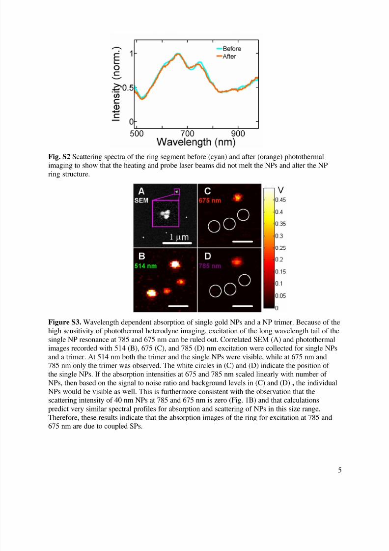
Fig. S2 Scattering spectra of the ring segment before (cyan) and after (orange) photothermal
imaging to show that the heating and probe laser beams did not melt the NPs and alter the NP
ring structure.
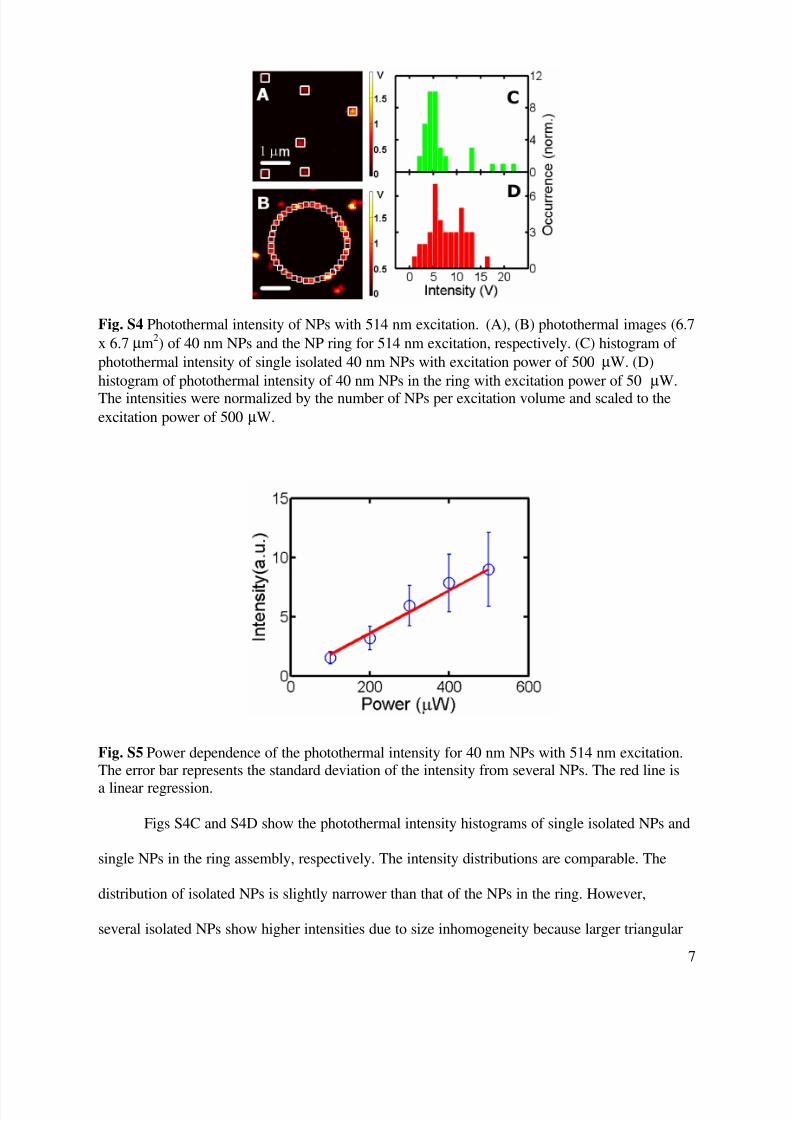
Figure S3. Wavelength dependent absorption of single gold NPs and a NP trimer. Because of the
high sensitivity of photothermal heterodyne imaging, excitation of the long wavelength tail of thesingle NP resonance at 785 and 675 nm can be ruled out. Correlated SEM (A) and photothermal
images recorded with 514 (B), 675 (C), and 785 (D) nm excitation were collected for single NPs
and a trimer. At 514 nm both the trimer and the single NPs were visible, while at 675 nm and785 nm only the trimer was observed. The white circles in (C) and (D) indicate the position of
the single NPs. If the absorption intensities at 675 and 785 nm scaled linearly with number of
NPs, then based on the signal to noise ratio and background levels in (C) and (D) , the individualNPs would be visible as well. This is furthermore consistent with the observation that thescattering intensity of 40 nm NPs at 785 and 675 nm is zero (Fig. 1B) and that calculations
predict very similar spectral profiles for absorption and scattering of NPs in this size range.
Therefore, these results indicate that the absorption images of the ring for excitation at 785 and675 nm are due to coupled SPs.

8/3/2019 Wei-Shun Chang et al- Low absorption losses of strongly coupled surface plasmons in nanoparticle assemblies
http://slidepdf.com/reader/full/wei-shun-chang-et-al-low-absorption-losses-of-strongly-coupled-surface-plasmons 12/26
6
Comparison of photothermal intensities of isolated NPs and NP ring at 514 nm
The photothermal intensities of single isolated NPs and NPs in the ring were compared to
show that at 514 nm the absorption intensity of the ring approximately scales with the number of
NPs per area. The same 40 nm NPs that were used to assemble the NP ring were drop-casted on
a glass slide followed by spin-casting a polyvinyl alcohol (PVA) film to ensure a homogenous
sounding medium. Single NPs were identified by SEM. The heating and probe wavelengths for
the photothermal measurements were 514 and 633 nm, respectively. For single NPs, the
excitation power was 500 µW. The excitation power for the NP ring was 50 µW to avoid
saturating the signal. The probe power was 800 µW for both measurements. Fig. S4A shows a
photothermal image of 40 nm NPs with 514 nm excitation. The intensities were integrated for
390 x 390 nm2 areas indicated by the white boxes, which was based on the optical resolution of
the photothermal images. Fig. S4B shows a photothermal image of the NP ring with 514 nm
excitation. The intensities were integrated for the same areas of 390 x 390 nm2
as shown again
by the white boxes. To compare the intensity per particle of single isolated NPs and individual
NPs in the ring assembly, the intensities of the different ring segments were normalized by the
number of NPs contained in each of the white boxes and then scaled to an excitation power of
500 µW. The number of NPs was obtained by overlaying the photothermal and SEM images.
Fig. S5 displays the power dependence of the photothermal intensity for 40 nm NPs with
514 nm excitation. The red line is a linear regression. The photothermal intensity scales linearly
with the excitation power which is consistent with previous results(2) and therefore justifies the
linear scaling factor used for the intensity comparison.
8/3/2019 Wei-Shun Chang et al- Low absorption losses of strongly coupled surface plasmons in nanoparticle assemblies
http://slidepdf.com/reader/full/wei-shun-chang-et-al-low-absorption-losses-of-strongly-coupled-surface-plasmons 13/26
7
Fig. S4 Photothermal intensity of NPs with 514 nm excitation. (A), (B) photothermal images (6.7
x 6.7 µm2) of 40 nm NPs and the NP ring for 514 nm excitation, respectively. (C) histogram of
photothermal intensity of single isolated 40 nm NPs with excitation power of 500 µW. (D)
histogram of photothermal intensity of 40 nm NPs in the ring with excitation power of 50 µW.The intensities were normalized by the number of NPs per excitation volume and scaled to the
excitation power of 500 µW.
Fig. S5 Power dependence of the photothermal intensity for 40 nm NPs with 514 nm excitation. The error bar represents the standard deviation of the intensity from several NPs. The red line is
a linear regression.
Figs S4C and S4D show the photothermal intensity histograms of single isolated NPs and
single NPs in the ring assembly, respectively. The intensity distributions are comparable. The
distribution of isolated NPs is slightly narrower than that of the NPs in the ring. However,
several isolated NPs show higher intensities due to size inhomogeneity because larger triangular

8/3/2019 Wei-Shun Chang et al- Low absorption losses of strongly coupled surface plasmons in nanoparticle assemblies
http://slidepdf.com/reader/full/wei-shun-chang-et-al-low-absorption-losses-of-strongly-coupled-surface-plasmons 14/26
8
NPs were also present as verified by correlated SEM imaging. The intensity histogram of single
NPs in the ring assembly is broader, but the maximum intensity is not as large as those of the
larger triangular NPs. Because the intensity of the NPs in the ring was normalized by the number
of NPs for each integration area, the contribution from larger triangular NPs is averaged with the
intensities of spherical NPs. This effect appears to lead to an apparent higher intensity per NP for
some areas and hence results in the broader intensity histogram observed for the NPs in the ring
assembly. Therefore, the intensities of single isolated NPs and NPs in the ring are comparable for
514 nm excitation.
Dark-field scattering is significantly less sensitive, making the same comparison to
individual 40 nm NPs more difficult. However, based on the similar intensity distributions for
absorption and scattering, as shown in Figs. 1E and 1H, the same conclusion should also apply
for scattering.
Fig. S6 Polarized photothermal images of the NP ring for 785 nm excitation. The arrows
represent the direction of excitation polarization.

8/3/2019 Wei-Shun Chang et al- Low absorption losses of strongly coupled surface plasmons in nanoparticle assemblies
http://slidepdf.com/reader/full/wei-shun-chang-et-al-low-absorption-losses-of-strongly-coupled-surface-plasmons 15/26
9
Fig. S7 Polarized scattering images of the NP ring recorded for a spectral window of 800 ± 20nm. The arrows represent the direction of detection polarization.
Fig. S8 Polarization dependence of the photothermal intensity for a single spherical NP (40 nm)with 514 nm excitation (black circle), a single nanorod (22 x 70 nm) with 785 nm excitation
(purple), and a single nanorod (25 x 75 nm) with 675 nm excitation (blue). The lines show fits of
the data points to ))(2cos1()( φ θ θ −+= M N I . The recovered modulation depth M was 0.08 for
the almost spherical NP consistent with an isotropic SP oscillation. In contrast, the modulation
depths M for the 22 x 70 nm and 25 x 75 nm nanorods were 0.96 and 1.02, respectively. This
confirms our ability to measure by polarization sensitive photothermal imaging a maximum
modulation depth of unity as expected for the longitudinal dipole mode of a nanorod.

8/3/2019 Wei-Shun Chang et al- Low absorption losses of strongly coupled surface plasmons in nanoparticle assemblies
http://slidepdf.com/reader/full/wei-shun-chang-et-al-low-absorption-losses-of-strongly-coupled-surface-plasmons 16/26
10
Fig S9 Unpolarized extinction spectra of local segments for different NP rings. The diameters of
the rings were 4.1(top), 4.6 (middle) and 5.6 (bottom) µm. The fact that the maxima of the
different SP modes did not change significantly for different ring diameters confirms that the
observed optical response originated from local NP segments and were not due to modes
delocalized over the entire ring. In addition, independent of the ring and the local segment all
spectra show SP resonances beyond 1000 nm that were assigned to SP coupling between
touching NPs.

8/3/2019 Wei-Shun Chang et al- Low absorption losses of strongly coupled surface plasmons in nanoparticle assemblies
http://slidepdf.com/reader/full/wei-shun-chang-et-al-low-absorption-losses-of-strongly-coupled-surface-plasmons 17/26
11
Fig. S10 FEM calculations of a local ring segment considering conductive coupling between
neighboring NPs. The NP geometry is given in (A) and (C) and the corresponding extinction
spectra are shown in (B) and (D). The excitation polarization was parallel to the long axis of the
NP arragment. In (A), two groups of NPs were touching (NPs #1, 2, and NPs #6, 7). In (C), three
groups of NPs were touching (NPs #1, 2, NPs #3, 4, 5, and NPs #6, 7).
Calculation of σσσσSCA for the NP ring
The scattering cross section σSCA for a ring of NPs was calculated by obtaining the ratio
of the scattering intensities from the NP ring (ISCA,Ring) and a single NP (ISCA,NP) and then
multiplying this ratio by the theoretical σSCA,NP of a single NP, as given in eq. S1.
NPSCA
ringSCA
NPSCAringSCA I
I
,
,
,, ×=σ σ (S1)
σSCA,NP was calculated by solving Maxwell’s equations for a known size of the NP and
the dielectric constants of the metal and surrounding medium. To obtain efficient scattering
intensities for single NPs at 800, 700, and 550 nm, we selected NPs with average sizes of 22 x 70
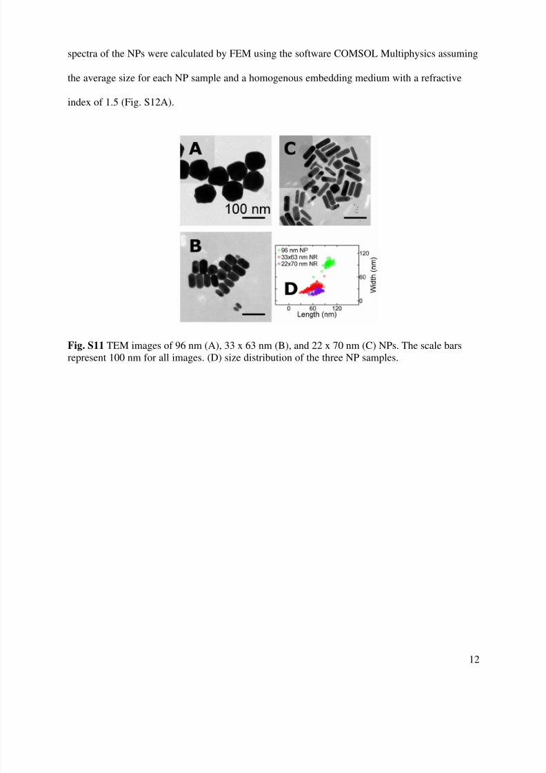
nm, 33 x 63 nm, and 96 nm which were first characterized by TEM (Fig. S11A-C). The size
distributions of each sample were 22 ± 4 x 70 ± 11 nm, 33 ± 5 x 63 ± 12 nm and 96 ± 7 nm (Fig.
11D), respectively. The error corresponds to the standard deviation of the NP size. The scattering
8/3/2019 Wei-Shun Chang et al- Low absorption losses of strongly coupled surface plasmons in nanoparticle assemblies
http://slidepdf.com/reader/full/wei-shun-chang-et-al-low-absorption-losses-of-strongly-coupled-surface-plasmons 18/26
12
spectra of the NPs were calculated by FEM using the software COMSOL Multiphysics assuming
the average size for each NP sample and a homogenous embedding medium with a refractive
index of 1.5 (Fig. S12A).
Fig. S11 TEM images of 96 nm (A), 33 x 63 nm (B), and 22 x 70 nm (C) NPs. The scale bars
represent 100 nm for all images. (D) size distribution of the three NP samples.

8/3/2019 Wei-Shun Chang et al- Low absorption losses of strongly coupled surface plasmons in nanoparticle assemblies
http://slidepdf.com/reader/full/wei-shun-chang-et-al-low-absorption-losses-of-strongly-coupled-surface-plasmons 19/26
13
Fig. S12 Calculated scattering and absorption cross sections of NPs. Calculated scattering (A)
and absorption (B) spectra of 96 nm (green), 33 x 63 nm (red) and 22 x 70 nm (purple) NPs
using the software COMSOL Multiphysics. The refractive index of the medium was chosen to be
1.5. The green, red, and purple bars in (A) mark the detection wavelengths of 550 ± 20, 700 ±
20, and 800 ± 20 nm, respectively. The green, red, and purple lines in (B) mark the excitation
wavelengths of 514, 675, and 785 nm, respectively.
In order to measure the scattering intensities of the single NPs, we drop-cast the NP
solution on a pre-cleaned glass slide, which was followed by spin-casting a thin layer of PVA
film to ensure a homogeneous surrounding medium with a refractive index of 1.5. The scattering
spectra of the single NPs were measured by dark-field microscopy and fit to a Lorentzian
function as expected for single NPs (Fig. S13). Only NPs with a peak wavelength within ± 10
nm of the predicted value based on the mean size of the experimental distribution (Fig. S12A)
were selected. About 20 NPs of each sample were chosen following this procedure. The
scattering intensities of the three NP samples with average sizes of 22 x 70, 33 x 63, and 96 nm
were then measured by dark-field microscopy using bandpass filters of 800 ± 20, 700 ± 20, and
550 ± 20 nm. Fig. S14A shows a scattering image of 96 nm NPs recorded with a bandpass filter

8/3/2019 Wei-Shun Chang et al- Low absorption losses of strongly coupled surface plasmons in nanoparticle assemblies
http://slidepdf.com/reader/full/wei-shun-chang-et-al-low-absorption-losses-of-strongly-coupled-surface-plasmons 20/26
14
of 550 ± 20 nm. The intensities of the selected NPs were integrated over a 850 x 850 nm2
area,
which was the resolution for the scattering image and is represented by the white boxes in Fig.
S14A. The 96 nm NPs were chosen because the scattering intensity of individual 40 nm NPs was
too low to yield reliable results. The same procedure was performed for the 22 x70 and 33 x 63
nm NPs using bandpass filters of 800 ± 20 and 700 ± 20 nm, respectively. In this way, we
determined the measured scattering intensities (ISCA,NP) for each sample.
Fig. S13 Scattering spectra of single NPs. Representative spectra are shown for NPs taken from
the samples with average sizes of 22 x 70 (A), 33 x 63 (B), and 96 nm (C). The black lines are
fits to a Lorentzian function, which is the expected line shape for single NPs.
8/3/2019 Wei-Shun Chang et al- Low absorption losses of strongly coupled surface plasmons in nanoparticle assemblies
http://slidepdf.com/reader/full/wei-shun-chang-et-al-low-absorption-losses-of-strongly-coupled-surface-plasmons 21/26
15
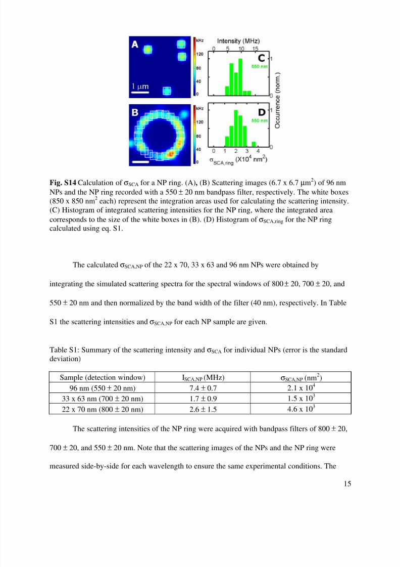
Fig. S14 Calculation of σSCA for a NP ring. (A), (B) Scattering images (6.7 x 6.7 µm2) of 96 nm
NPs and the NP ring recorded with a 550 ± 20 nm bandpass filter, respectively. The white boxes
(850 x 850 nm2 each) represent the integration areas used for calculating the scattering intensity.
(C) Histogram of integrated scattering intensities for the NP ring, where the integrated area
corresponds to the size of the white boxes in (B). (D) Histogram of σSCA,ring for the NP ring
calculated using eq. S1.
The calculated σSCA,NP of the 22 x 70, 33 x 63 and 96 nm NPs were obtained by
integrating the simulated scattering spectra for the spectral windows of 800 ± 20, 700 ± 20, and
550 ± 20 nm and then normalized by the band width of the filter (40 nm), respectively. In Table
S1 the scattering intensities and σSCA,NP for each NP sample are given.
Table S1: Summary of the scattering intensity and σSCA for individual NPs (error is the standard
deviation)
Sample (detection window) ISCA,NP (MHz) σSCA,NP (nm2)
96 nm (550 ± 20 nm) 7.4 ± 0.7 2.1 x 10⁴
33 x 63 nm (700 ± 20 nm) 1.7 ± 0.9 1.5 x 10³
22 x 70 nm (800 ± 20 nm) 2.6 ± 1.5 4.6 x 10³
The scattering intensities of the NP ring were acquired with bandpass filters of 800 ± 20,
700 ± 20, and 550 ± 20 nm. Note that the scattering images of the NPs and the NP ring were
measured side-by-side for each wavelength to ensure the same experimental conditions. The

8/3/2019 Wei-Shun Chang et al- Low absorption losses of strongly coupled surface plasmons in nanoparticle assemblies
http://slidepdf.com/reader/full/wei-shun-chang-et-al-low-absorption-losses-of-strongly-coupled-surface-plasmons 22/26
16
intensities of the ring segments (ISCA,ring) were also acquired by integrating areas of 850 x 850
nm2
along the ring to compare to the single NPs. Fig. S14B shows the scattering image of the NP
ring taken with a bandpass filter for 550 ± 20 nm. Each white box represents the integration area
used for the intensity calculation. The ring was divided into 24 segments according to the
experimental resolution. Fig. S14C shows the histogram of the scattering intensities of these 24
segments. Values for σSCA,ring of the ring were calculated using eq. S1. Table S2 shows the mean
scattering intensity and σSCA,ring of the24 ring segments for wavelengths of 800 ± 20, 700 ± 20,
and 550 ± 20 nm.
Table S2: Summary of the mean scattering intensity, σSCA,ring, and σSCA for the 24 ring segments(error is the standard deviation)
Detection window ISCA,ring (MHz) σSCA,ring (nm2) σSCA (nm
2)
550 ± 20 nm 7.9 ± 2.0 (2.2 ± 0.6) x 104
560 ± 128
700 ± 20 nm 29.0 ± 8.3 (2.5 ± 0.7) x 104
656 ± 177
800 ± 20 nm 12.8 ± 4.8 (2.3 ± 0.8)x 104 608 ± 247
Fig. S14D displays the σSCA,ringt histogram of the NP ring. The numbers of NPs for each
ring segment were also acquired by overlaying Fig. S14B with the SEM image and counting the
number of NPs for each white box (Fig. S15A). The normalized σSCA, which represents σSCA,ring
per NP, was calculated by σSCA,ring / N where N is the number of NPs for each ring segment. σSCA
at 800 ± 20, 700 ± 20, and 550 ± 20 nm are also listed in Table S2.

8/3/2019 Wei-Shun Chang et al- Low absorption losses of strongly coupled surface plasmons in nanoparticle assemblies
http://slidepdf.com/reader/full/wei-shun-chang-et-al-low-absorption-losses-of-strongly-coupled-surface-plasmons 23/26
17
Fig. S15 Scattering (A) and absorption (B) images overlaid with the SEM image allowing the
determination of the average number of NPs per integration area.
Calculation of σσσσABS for the NP ring
The calculation of σABS for the NP ring was similar to that of σSCA. Photothermal images
were acquired from the same NPs analyzed in the scattering experiments using circularly
polarized excitation. The excitation wavelengths for the 22 x 70, 33 x 63, and 96 nm NPs were
785, 675, and 514 nm, respectively. The excitation and probe powers ranged between 8 - 54 and
99 -127 kW/cm2
for the different samples to avoid signal saturation. Fig. S16A shows a
photothermal image of 96 nm NPs excited at 514 nm. Each white box corresponds to the area
used to calculate the intensity, which was chosen to be 390 x 390 nm2
based on the optical
resolution of the photothermal images. Photothermal images for 22 x70 and 33 x 63 nm NPs
were also measured, using 785 and 675 nm excitation. The measured absorption intensities
(IABS,NP) of each sample are given in Table S3. The calculated σABS,NP for these samples at 785,
675, and 514 nm using the simulated spectra in Fig. S13B are also listed in Table S3.

8/3/2019 Wei-Shun Chang et al- Low absorption losses of strongly coupled surface plasmons in nanoparticle assemblies
http://slidepdf.com/reader/full/wei-shun-chang-et-al-low-absorption-losses-of-strongly-coupled-surface-plasmons 24/26
18
Fig. S16 Calculation of σABS for a NP ring. (A), (B) Photothermal images (6.7 x 6.7 µm2) of 96
nm NPs and the NP ring for 514 nm excitation, respectively. The white boxes (390 x 390 nm2)
present the integration areas used for the intensity calculation. (C) Histogram of integrated
absorption intensities for the NP ring, where the integrated area corresponds to the size of the
white boxes in (B). (D) Histogram of σABS,ring for the NP ring calculated using eq. S2.
Table S3: Summary of the absorption intensity and σABS for individual NPs (error is standard the
deviation)
Sample (excitation wavelength) IABS,NP (V) σABS.NP (nm2)
96 nm (514 nm) 9.6 ± 4.8 1.5 x 10
4
33 x 63 nm (675 nm) 14.1 ± 6.0 4.5 x 10³
22 x 70 nm (785 nm) 3.2 ± 1.2 9.6 x 10³
The photothermal images of the NP ring were also measured with 785, 675, and 514 nm
excitation and circular polarization. The photothermal images of the NP ring and NPs were again
measured side-by-side for each wavelength to ensure the same experimental conditions. Fig.
S16B shows the photothermal image of the NP ring with 514 nm excitation. The white boxes
represent the same integration areas for calculating the experimental absorption intensity as was
used for the single NPs (390 x 390 nm2). The ring was therefore divided into 40 segments. Fig.
8/3/2019 Wei-Shun Chang et al- Low absorption losses of strongly coupled surface plasmons in nanoparticle assemblies
http://slidepdf.com/reader/full/wei-shun-chang-et-al-low-absorption-losses-of-strongly-coupled-surface-plasmons 25/26
19
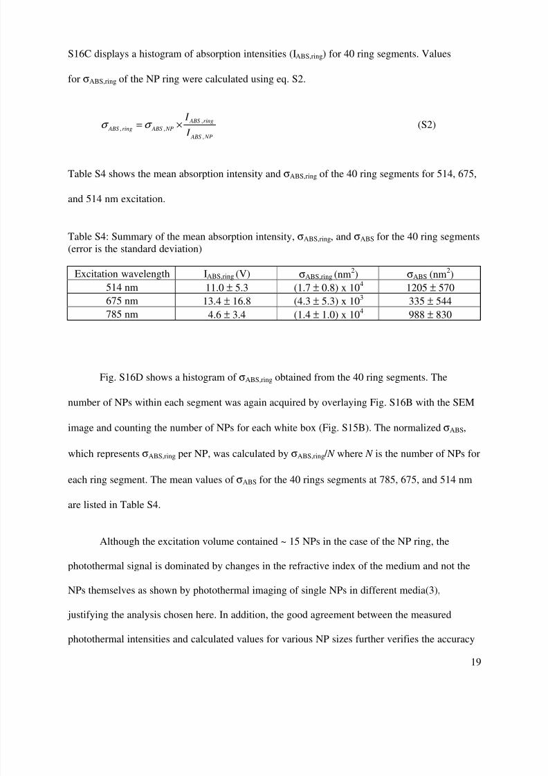
S16C displays a histogram of absorption intensities (IABS,ring) for 40 ring segments. Values
for σABS,ring of the NP ring were calculated using eq. S2.
NP ABS
ring ABS
NP ABSring ABS
I
I
,
,
,, ×=σ σ (S2)
Table S4 shows the mean absorption intensity and σABS,ring of the 40 ring segments for 514, 675,
and 514 nm excitation.
Table S4: Summary of the mean absorption intensity, σABS,ring, and σABS for the 40 ring segments
(error is the standard deviation)
Excitation wavelength IABS,ring (V) σABS,ring (nm2) σABS (nm2)
514 nm 11.0 ± 5.3 (1.7 ± 0.8) x 104
1205 ± 570
675 nm 13.4 ± 16.8 (4.3 ± 5.3) x 103
335 ± 544
785 nm 4.6 ± 3.4 (1.4 ± 1.0) x 104
988 ± 830
Fig. S16D shows a histogram of σABS,ring obtained from the 40 ring segments. The
number of NPs within each segment was again acquired by overlaying Fig. S16B with the SEM
image and counting the number of NPs for each white box (Fig. S15B). The normalized σABS,
which represents σABS,ring per NP, was calculated by σABS,ring / N where N is the number of NPs for
each ring segment. The mean values of σABS for the 40 rings segments at 785, 675, and 514 nm
are listed in Table S4.
Although the excitation volume contained ~ 15 NPs in the case of the NP ring, the
photothermal signal is dominated by changes in the refractive index of the medium and not the
NPs themselves as shown by photothermal imaging of single NPs in different media(3),
justifying the analysis chosen here. In addition, the good agreement between the measured
photothermal intensities and calculated values for various NP sizes further verifies the accuracy
8/3/2019 Wei-Shun Chang et al- Low absorption losses of strongly coupled surface plasmons in nanoparticle assemblies
http://slidepdf.com/reader/full/wei-shun-chang-et-al-low-absorption-losses-of-strongly-coupled-surface-plasmons 26/26
of photothermal imaging in determining SP absorption regardless of the volume of the NPs
probed in the excitation area(4).
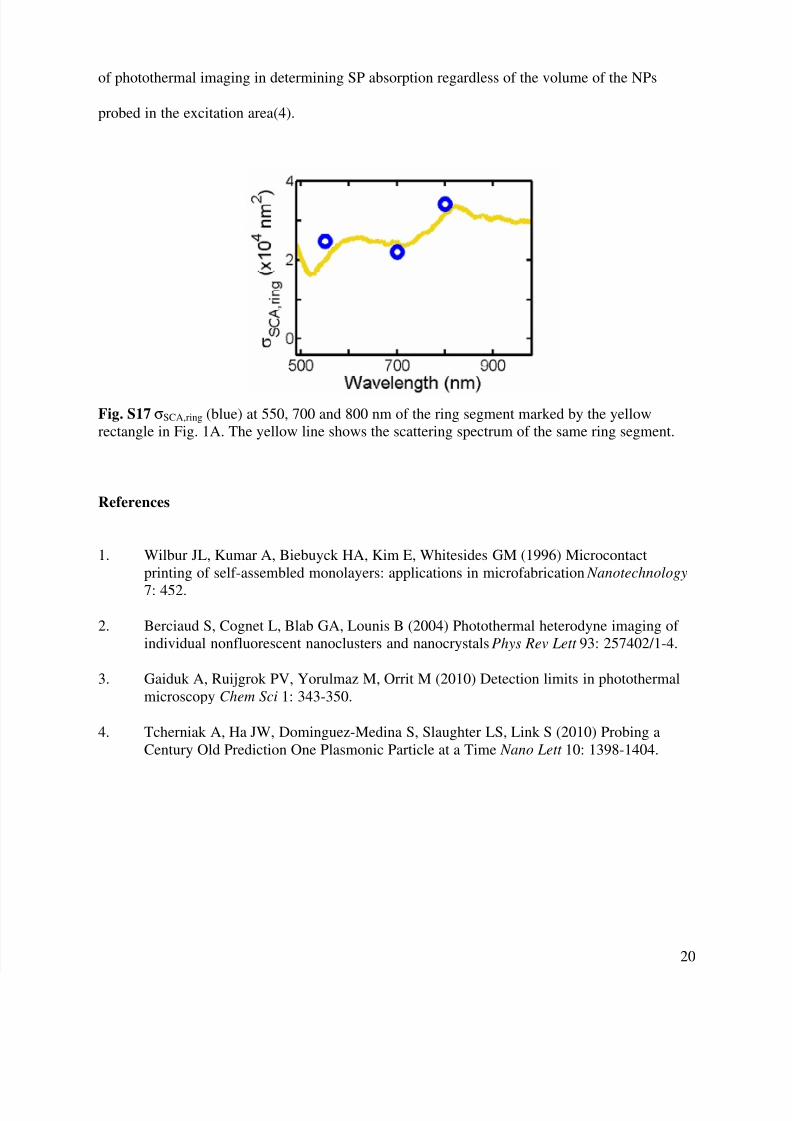
Fig. S17 σSCA,ring (blue) at 550, 700 and 800 nm of the ring segment marked by the yellow
rectangle in Fig. 1A. The yellow line shows the scattering spectrum of the same ring segment.
References
1. Wilbur JL, Kumar A, Biebuyck HA, Kim E, Whitesides GM (1996) Microcontact
printing of self-assembled monolayers: applications in microfabrication Nanotechnology
7: 452.
2. Berciaud S, Cognet L, Blab GA, Lounis B (2004) Photothermal heterodyne imaging of
individual nonfluorescent nanoclusters and nanocrystals Phys Rev Lett 93: 257402/1-4.
3. Gaiduk A, Ruijgrok PV, Yorulmaz M, Orrit M (2010) Detection limits in photothermal
microscopy Chem Sci 1: 343-350.
4. Tcherniak A, Ha JW, Dominguez-Medina S, Slaughter LS, Link S (2010) Probing a
Century Old Prediction One Plasmonic Particle at a Time Nano Lett 10: 1398-1404.