wcd9311 audio codec - qualcomm developer network · wcd9311 audio codec device specification...
TRANSCRIPT

WCD9311 Audio Codec
Device Specification
LM80-P0598-3 Rev. B
September 2016
© 2015-2016 Qualcomm Technologies, Inc. All rights reserved.
Qualcomm Snapdragon is a product of Qualcomm Technologies, Inc. Other Qualcomm products referenced herein are products ofQualcomm Technologies, Inc. or its other subsidiaries.
DragonBoard, Qualcomm, and Snapdragon are trademarks of Qualcomm Incorporated, registered in the United States and other countries. Other product and brand names may be trademarks or registered trademarks of their respective owners.
This technical data may be subject to U.S. and international export, re-export, or transfer (“export”) laws. Diversion contrary to U.S.and international law is strictly prohibited.
Use of this document is subject to the license set forth In Exhibit 1.
Qualcomm Technologies, Inc.
5775 Morehouse Drive San Diego, CA 92121
U.S.A.
LM80-P0598-3 Rev. B

LM80-P0598-3 Rev. B MAY CONTAIN U.S. AND INTERNATIONAL EXPORT CONTROLLED INFORMATION 2
Revision history
Revision Date Description
A June 1, 2015 Initial release
B September 23, 2016 Updated to E part

LM80-P
Contents
1 Introduction . . . . . . . . . . . . . . . . . . . . . . . . . . . . . . . . . . . . . . . . . . . . . . . . . . . . . . . . . . . . . . . 7
1.1 Documentation overview . . . . . . . . . . . . . . . . . . . . . . . . . . . . . . . . . . . . . . . . . . . . . . . . . . . 71.2 WCD9311 device introduction . . . . . . . . . . . . . . . . . . . . . . . . . . . . . . . . . . . . . . . . . . . . . . . 81.3 WCD9311 features . . . . . . . . . . . . . . . . . . . . . . . . . . . . . . . . . . . . . . . . . . . . . . . . . . . . . . . 101.4 Terms and acronyms . . . . . . . . . . . . . . . . . . . . . . . . . . . . . . . . . . . . . . . . . . . . . . . . . . . . . . 151.5 Special marks . . . . . . . . . . . . . . . . . . . . . . . . . . . . . . . . . . . . . . . . . . . . . . . . . . . . . . . . . . . 16
2 Pin Definitions . . . . . . . . . . . . . . . . . . . . . . . . . . . . . . . . . . . . . . . . . . . . . . . . . . . . . . . . . . . . 18
2.1 I/O parameter definitions . . . . . . . . . . . . . . . . . . . . . . . . . . . . . . . . . . . . . . . . . . . . . . . . . . 202.2 Pin descriptions . . . . . . . . . . . . . . . . . . . . . . . . . . . . . . . . . . . . . . . . . . . . . . . . . . . . . . . . . . 20
3 Electrical Specifications . . . . . . . . . . . . . . . . . . . . . . . . . . . . . . . . . . . . . . . . . . . . . . . . . . 25
3.1 Absolute maximum ratings . . . . . . . . . . . . . . . . . . . . . . . . . . . . . . . . . . . . . . . . . . . . . . . . . 253.2 Recommended operating conditions . . . . . . . . . . . . . . . . . . . . . . . . . . . . . . . . . . . . . . . . . 263.3 DC power characteristics . . . . . . . . . . . . . . . . . . . . . . . . . . . . . . . . . . . . . . . . . . . . . . . . . . 273.4 Powerup sequence . . . . . . . . . . . . . . . . . . . . . . . . . . . . . . . . . . . . . . . . . . . . . . . . . . . . . . . 303.5 Digital logic characteristics . . . . . . . . . . . . . . . . . . . . . . . . . . . . . . . . . . . . . . . . . . . . . . . . 303.6 Audio inputs and Tx processing . . . . . . . . . . . . . . . . . . . . . . . . . . . . . . . . . . . . . . . . . . . . . 303.7 Audio outputs and Rx processing . . . . . . . . . . . . . . . . . . . . . . . . . . . . . . . . . . . . . . . . . . . . 363.8 Digital I/Os and digital processing . . . . . . . . . . . . . . . . . . . . . . . . . . . . . . . . . . . . . . . . . . . 473.9 Support circuits – analog . . . . . . . . . . . . . . . . . . . . . . . . . . . . . . . . . . . . . . . . . . . . . . . . . . 503.10 Support circuits – digital . . . . . . . . . . . . . . . . . . . . . . . . . . . . . . . . . . . . . . . . . . . . . . . . . . . 51
4 Mechanical Information . . . . . . . . . . . . . . . . . . . . . . . . . . . . . . . . . . . . . . . . . . . . . . . . . . . 52
4.1 Device physical dimensions . . . . . . . . . . . . . . . . . . . . . . . . . . . . . . . . . . . . . . . . . . . . . . . . 524.2 Part marking . . . . . . . . . . . . . . . . . . . . . . . . . . . . . . . . . . . . . . . . . . . . . . . . . . . . . . . . . . . . 544.3 Device ordering information . . . . . . . . . . . . . . . . . . . . . . . . . . . . . . . . . . . . . . . . . . . . . . . 554.4 Device moisture-sensitivity level . . . . . . . . . . . . . . . . . . . . . . . . . . . . . . . . . . . . . . . . . . . . 564.5 Thermal characteristics . . . . . . . . . . . . . . . . . . . . . . . . . . . . . . . . . . . . . . . . . . . . . . . . . . . . 56
5 Carrier, Storage, & Handling Information . . . . . . . . . . . . . . . . . . . . . . . . . . . . . . . . . . 57
5.1 Carrier . . . . . . . . . . . . . . . . . . . . . . . . . . . . . . . . . . . . . . . . . . . . . . . . . . . . . . . . . . . . . . . . . 575.2 Storage . . . . . . . . . . . . . . . . . . . . . . . . . . . . . . . . . . . . . . . . . . . . . . . . . . . . . . . . . . . . . . . . 58
0598-3 Rev. B MAY CONTAIN U.S. AND INTERNATIONAL EXPORT CONTROLLED INFORMATION 3

LM80-P
WCD9311 Audio Codec Device Specification Contents
6 PCB Mounting Guidelines . . . . . . . . . . . . . . . . . . . . . . . . . . . . . . . . . . . . . . . . . . . . . . . . 60
6.1 Land pad and stencil design . . . . . . . . . . . . . . . . . . . . . . . . . . . . . . . . . . . . . . . . . . . . . . . . 606.2 SMT development and characterization . . . . . . . . . . . . . . . . . . . . . . . . . . . . . . . . . . . . . . . 606.3 SMT peak package-body temperature . . . . . . . . . . . . . . . . . . . . . . . . . . . . . . . . . . . . . . . . 616.4 SMT process verification . . . . . . . . . . . . . . . . . . . . . . . . . . . . . . . . . . . . . . . . . . . . . . . . . . 61
7 Part Reliability . . . . . . . . . . . . . . . . . . . . . . . . . . . . . . . . . . . . . . . . . . . . . . . . . . . . . . . . . . . . 62
7.1 Reliability qualification summary . . . . . . . . . . . . . . . . . . . . . . . . . . . . . . . . . . . . . . . . . . . 62
Appendix A1 Terms and Acronyms. . . . . . . . . . . . . . . . . . . . . . . . . . . . . . . . . . . . . . . . . . . . . . . . . . . . . . . . . . . 64
Appendix A2Exhibit 1 . . . . . . . . . . . . . . . . . . . . . . . . . . . . . . . . . . . . . . . . . . . . . . . . . . . . . . . . . . . . . . . . . . . . 66
0598-3 Rev. B MAY CONTAIN U.S. AND INTERNATIONAL EXPORT CONTROLLED INFORMATION 4

LM80-P0598-3 Rev. B MAY CONTAIN U.S. AND INTERNATIONAL EXPORT CONTROLLED INFORMATION 5.
WCD9311 Audio Codec Device Specification Contents
Figures
Figure 1-1 WCD9311 IC in a typical application . . . . . . . . . . . . . . . . . . . . . . . . . . . . . . . . . . . . . 9Figure 2-1 WCD9311 IC pin assignments (top view) . . . . . . . . . . . . . . . . . . . . . . . . . . . . . . . . . 19Figure 3-1 THD + N (0 dB gain) . . . . . . . . . . . . . . . . . . . . . . . . . . . . . . . . . . . . . . . . . . . . . . . . . 32Figure 3-2 THD + N (18 dB gain) . . . . . . . . . . . . . . . . . . . . . . . . . . . . . . . . . . . . . . . . . . . . . . . . 32Figure 3-3 Frequency response (16 kHz) . . . . . . . . . . . . . . . . . . . . . . . . . . . . . . . . . . . . . . . . . . 33Figure 3-4 Frequency response (48 kHz) . . . . . . . . . . . . . . . . . . . . . . . . . . . . . . . . . . . . . . . . . . 33Figure 3-5 Frequency response (192 kHz) . . . . . . . . . . . . . . . . . . . . . . . . . . . . . . . . . . . . . . . . . 34Figure 3-6 THD + N 8 kHz (EAR PA) . . . . . . . . . . . . . . . . . . . . . . . . . . . . . . . . . . . . . . . . . . . . 38Figure 3-7 Frequency response 16 kHz (EAR PA) . . . . . . . . . . . . . . . . . . . . . . . . . . . . . . . . . . . 38Figure 3-8 THD + N 48 kHz (HPH PA) . . . . . . . . . . . . . . . . . . . . . . . . . . . . . . . . . . . . . . . . . . . 41Figure 3-9 Frequency response 48 kHz (HPH PA) . . . . . . . . . . . . . . . . . . . . . . . . . . . . . . . . . . . 41Figure 3-10 THD + N 192 kHz (LINE_OUT PA) . . . . . . . . . . . . . . . . . . . . . . . . . . . . . . . . . . . 46Figure 3-11 Frequency response 192 kHz (LINE_OUT PA) . . . . . . . . . . . . . . . . . . . . . . . . . . . 46Figure 3-12 Received clock signal constraints . . . . . . . . . . . . . . . . . . . . . . . . . . . . . . . . . . . . . . 47Figure 3-13 I2S transmitter timing diagram . . . . . . . . . . . . . . . . . . . . . . . . . . . . . . . . . . . . . . . . 48Figure 3-14 I2S receiver timing diagram . . . . . . . . . . . . . . . . . . . . . . . . . . . . . . . . . . . . . . . . . . 48Figure 3-15 WCD9311 received clock signal constraints . . . . . . . . . . . . . . . . . . . . . . . . . . . . . . 49Figure 4-1 86 pin CSP (6.0 × 6.0 × 1.27 mm) outline drawing . . . . . . . . . . . . . . . . . . . . . . . . . . 53Figure 4-2 WCD9311 IC part marking (top view – not to scale) . . . . . . . . . . . . . . . . . . . . . . . . 54Figure 4-3 WDC9311 device identification code . . . . . . . . . . . . . . . . . . . . . . . . . . . . . . . . . . . . 55Figure 5-1 Carrier tape drawing with part orientation . . . . . . . . . . . . . . . . . . . . . . . . . . . . . . . . . 57Figure 5-2 Tape handling . . . . . . . . . . . . . . . . . . . . . . . . . . . . . . . . . . . . . . . . . . . . . . . . . . . . . . 58

LM80-P0598-3 Rev. B MAY CONTAIN U.S. AND INTERNATIONAL EXPORT CONTROLLED INFORMATION 6
WCD9311 Audio Codec Device Specification Contents
Tables
Table 1-1 Primary WCD9311 documentation . . . . . . . . . . . . . . . . . . . . . . . . . . . . . . . . . . . . . . . . 7Table 1-2 Key WCD9311 features . . . . . . . . . . . . . . . . . . . . . . . . . . . . . . . . . . . . . . . . . . . . . . . . 13Table 1-3 Terms and acronyms . . . . . . . . . . . . . . . . . . . . . . . . . . . . . . . . . . . . . . . . . . . . . . . . . . 15Table 1-4 Special marks . . . . . . . . . . . . . . . . . . . . . . . . . . . . . . . . . . . . . . . . . . . . . . . . . . . . . . . 16Table 2-1 I/O description (pad type) parameters . . . . . . . . . . . . . . . . . . . . . . . . . . . . . . . . . . . . . 20Table 2-2 Pin descriptions – analog outputs and Rx processing . . . . . . . . . . . . . . . . . . . . . . . . . 21Table 2-3 Pin descriptions – analog inputs and Tx processing . . . . . . . . . . . . . . . . . . . . . . . . . . 21Table 2-4 Pin descriptions – digital data I/Os . . . . . . . . . . . . . . . . . . . . . . . . . . . . . . . . . . . . . . . 22Table 2-5 Pin descriptions – support functions (analog) . . . . . . . . . . . . . . . . . . . . . . . . . . . . . . . 23Table 2-6 Pin descriptions – support functions (digital) . . . . . . . . . . . . . . . . . . . . . . . . . . . . . . . 23Table 2-7 Pin descriptions – Power supply pins . . . . . . . . . . . . . . . . . . . . . . . . . . . . . . . . . . . . . 24Table 2-8 Pin descriptions – Ground pins . . . . . . . . . . . . . . . . . . . . . . . . . . . . . . . . . . . . . . . . . . 24Table 2-9 Pin descriptions – Do not connect (DNC) pins . . . . . . . . . . . . . . . . . . . . . . . . . . . . . . 24Table 3-1 Absolute maximum ratings . . . . . . . . . . . . . . . . . . . . . . . . . . . . . . . . . . . . . . . . . . . . . 25Table 3-2 Recommended operating conditions . . . . . . . . . . . . . . . . . . . . . . . . . . . . . . . . . . . . . . 26Table 3-3 Power supply peak current . . . . . . . . . . . . . . . . . . . . . . . . . . . . . . . . . . . . . . . . . . . . . 27Table 3-4 Power consumption for typical use cases . . . . . . . . . . . . . . . . . . . . . . . . . . . . . . . . . . 28Table 3-5 Digital I/O characteristics . . . . . . . . . . . . . . . . . . . . . . . . . . . . . . . . . . . . . . . . . . . . . . 30Table 3-6 Analog input through digital serial interface performance . . . . . . . . . . . . . . . . . . . . . 30Table 3-7 Digital microphone input through digital serial interface performance . . . . . . . . . . . 35Table 3-8 Serial interface through mono EAR output . . . . . . . . . . . . . . . . . . . . . . . . . . . . . . . . . 36Table 3-9 Serial interface through stereo HPH output . . . . . . . . . . . . . . . . . . . . . . . . . . . . . . . . 39Table 3-10 Serial interface through stereo LINE output . . . . . . . . . . . . . . . . . . . . . . . . . . . . . . . 42Table 3-11 Serial interface through mono LINE outputs . . . . . . . . . . . . . . . . . . . . . . . . . . . . . . 44Table 3-12 Clock input timing requirements . . . . . . . . . . . . . . . . . . . . . . . . . . . . . . . . . . . . . . . . 47Table 3-13 Data output timing characteristics . . . . . . . . . . . . . . . . . . . . . . . . . . . . . . . . . . . . . . . 47Table 3-14 Data input timing requirements . . . . . . . . . . . . . . . . . . . . . . . . . . . . . . . . . . . . . . . . . 47Table 3-15 Supported I2S standards and exceptions . . . . . . . . . . . . . . . . . . . . . . . . . . . . . . . . . . 48Table 3-16 Master transmitter with data rate of 16 MHz . . . . . . . . . . . . . . . . . . . . . . . . . . . . . . 48Table 3-17 Slave receiver with data rate of 16 MHz . . . . . . . . . . . . . . . . . . . . . . . . . . . . . . . . . . 48Table 3-18 Supported I2C standards and exceptions . . . . . . . . . . . . . . . . . . . . . . . . . . . . . . . . . . 49Table 3-19 Digital microphone timing . . . . . . . . . . . . . . . . . . . . . . . . . . . . . . . . . . . . . . . . . . . . 49Table 3-20 Microphone bias performance . . . . . . . . . . . . . . . . . . . . . . . . . . . . . . . . . . . . . . . . . . 50Table 3-21 Analog input to AUX_PGA to output PA specifications . . . . . . . . . . . . . . . . . . . . . 51Table 4-1 Part marking line descriptions . . . . . . . . . . . . . . . . . . . . . . . . . . . . . . . . . . . . . . . . . . . 54Table 4-2 Device identification code/ordering information details . . . . . . . . . . . . . . . . . . . . . . . 55Table 4-3 Source configuration code . . . . . . . . . . . . . . . . . . . . . . . . . . . . . . . . . . . . . . . . . . . . . . 55Table 4-4 Device thermal resistance . . . . . . . . . . . . . . . . . . . . . . . . . . . . . . . . . . . . . . . . . . . . . . 56Table 6-1 Typical SMT reflow profile conditions (for reference only) . . . . . . . . . . . . . . . . . . . . 61Table 7-1 Reliability evaluation summary . . . . . . . . . . . . . . . . . . . . . . . . . . . . . . . . . . . . . . . . . . 62Table A1-1 Terms and acronyms . . . . . . . . . . . . . . . . . . . . . . . . . . . . . . . . . . . . . . . . . . . . . . . . . 64

LM80-P
1 Introduction
1.1 Documentation overview
This document provides a description of chipset capabilities. Not all features are available, nor are all features supported in the software.
NOTE Enabling some features may require additional licensing fees.
Technical information for the WCD9311 IC is primarily covered by the documents listed in Table 1-1, and all should be studied for a thorough understanding of the device and its applications.
This WCD9311 device specification is organized as follows:
Table 1-1 Primary WCD9311 documentation
Document Title/description
WCD9311 Device
Specification (this document)
Conveys all WCD9311 IC electrical and mechanical specifications. Additional material includes pin assignments; shipping, storage, and handling instructions; PCB mounting guidelines; and part reliability. This document can be used by company purchasing departments to facilitate procurement.
APQ8064E Chipset Data
Sheet
Provides guidelines for the APQ8064E audio module, including a comprehensive overview of the WCD9311 audio codec IC.
I2C Bus Specification, version 2.1,
January 2000
Philips Semiconductor document number 9398 393 40011.This document can be found at
http://i2c2p.twibright.com/spec/i2c.pdf
I2S Bus Specification, version 2.1,
February 1986
Philips Semiconductor 2S Bus Specification,document.This document can be found at https://www.sparkfun.com/datasheets/BreakoutBoards/I2SBUS.pdf.
SLIMbus Specification
Serial Low-power Inter-chip Media Bus (SLIMbus) Specification. See http://www.mipi.org/specifications/serial-low-power-inter-chip-media-bus-slimbussm-specification
Chapter 1 Provides an overview of the WCD9311 documentation, gives a high-level functional description of the device, lists the device features, and defines marking conventions used throughout this document.
Chapter 2 Defines the device pin assignments.
0598-3 Rev. B MAY CONTAIN U.S. AND INTERNATIONAL EXPORT CONTROLLED INFORMATION 7.

LM80-P
WCD9311 Audio Codec Device Specification Introduction
1.2 WCD9311 device introduction
The WCD9311 IC is a standalone audio codec IC that supports multimedia solutions, including the APQ8064E chipset. Key WCD9311 functions include:
Serial low-power inter-chip media bus (SLIMbus) for access to on-chip digital audio channels with fewer pins relative to inter-IC sound (I2S) bus
Seven analog input ports and eight analog output ports
Seven analog-to-digital converters (ADCs) and eight digital-to-analog converters (DACs)
Six digital microphone inputs (three clock/data pairs)
Sidetone sample rate converter and infinite impulse response (IIR) filters for better performance and lower latency
The WCD9311 IC supports two I/O operating modes: SLIMbus and I2S (selected using a dedicated hardware mode control pin). SLIMbus is the primary mode that provides access to all the audio codec paths and features, while I2S provides access to fewer paths but maintains compatibility with earlier generation ICs. An example WCD9311 application is shown in Figure 1-1; this example uses the APQ8064E chipset with the primary WCD/APQ interface implemented via SLIMbus.
This highly integrated IC is very small – it uses the 6.0 × 6.0 × 1.27 mm, 86 pin chip-scale package (86 CSP) – and is supplemented by IC processing (such as the APQ8064E IC) to create an audio solution that reduces part count and PCB area. Companion chipsets ensure hardware and software compatibility to simplify the design cycle and reduce OEM time-to-market.
The WCD9311 IC uses low-power 65 nm CMOS fabrication technology, making it perfectly suited for battery-operated devices where power consumption and performance are critical.
Chapter 3 Defines the device electrical performance specifications, including absolute maximum and recommended operating conditions.
Chapter 4 Provides IC mechanical information, including dimensions, markings, ordering information, moisture sensitivity, and thermal characteristics.
Chapter 5 Discusses shipping, storage, and handling of the WCD9311 devices.
Chapter 6 Presents procedures and specifications for mounting the WCD9311 device onto printed circuit boards (PCBs).
Chapter 7 Presents WCD9311 device reliability data, including a definition of the qualification samples and a summary of qualification test results.
Appendix A Defines the terms and acronym used in this document
Appendix B Provides the terms of Exhibit 1.
0598-3 Rev. B MAY CONTAIN U.S. AND INTERNATIONAL EXPORT CONTROLLED INFORMATION 8.

WCD Introduction
ReLM 9
Figu
EG from circuits
outputrge pump puts
bias puts
pensation acitors
HC61
AT
dwired PM8921
IO_34
Quad digital m icrophones
APQ8064
9311 Audio Codec Device Specification
80-P0598-3 Rev. B MAY CONTAIN U.S. AND INTERNATIONAL EXPORT CONTROLLED INFORMATION.
re 1-1 WCD9311 IC in a typical application
EarpieceClass G125 mW32
ster
eo
Headset M IC
DC
po
wer
circ
uits VR
PMLDOchaout
MICout
comcap
EAROP
HPH_LP
LINE_OUT1
MIC_IN5_P
ADC
ADC
AU
X P
GA
mix
ing
with
all
DA
C o
utp
uts
DAC
DAC
DAC
MIC_IN5_M
MIC_IN6_P
MIC_IN6_M
MIC_IN3_P
ADC
ADCMIC_IN3_M
MIC_IN4_P
MIC_IN4_M
MIC_IN1_P
ADC
ADCMIC_IN1_M
MIC_IN2_P
MIC_IN2_M
HPH_RM
EAROM
aux_pga_l
aux_pga_r
LINE_OUT2
LINE_OUT3
LINE_OUT4
LINE_OUT5
DAC
DAC
DAC
DAC
GND_HPH_REF
adc1
adc2
adc5
adc6
adc3
adc4
dac1
dac2
dac3
dac4
dac5
dac6
dac7
ADCadc7
Rx
& T
x D
igita
l Pro
cess
ing
and
Act
ive
Noi
se C
anc
ella
tion
–M
ulti
plex
ing
–M
ixin
g
–
Infin
ite I
mpu
lse
Re
spon
se (
IIR)
Filt
erin
g
–
Sam
ple
Ra
te C
onv
ers
ion
(SR
C)
sta
tus
&
con
trol
W CD9311
I2C_SCL
I2C_SDA
RX_I2S_SCK
‘R1’ = RX_I2S_SD1
RX_I2S_W S
TX_I2S_SCK
‘T1’ = TX_I2S_SD1
‘R2’ = RX_I2S_SD2
TX_I2S_W S
Rx
I2S
in
terf
ace
DM IC56_DA (R1)
DMIC56_CK (R2)
Tx
I2S
in
terf
ace
I2C
inte
rfa
ce
SB_DA (T2)
SB_CK (T1)
SL
IMbu
s in
terf
ace
DM
IC
inte
rfa
ces
‘T2’ = TX_I2S_SD2
DMIC34_DATA
DMIC34_CLK
DMIC12_DATA
DMIC12_CLKdmic1
dmic2
dmic3
dmic4
dmic5
dmic6
MCLK
RESET
IF_MODE
INT_OUT
clo
ck
circ
uits
Headset M IC
eadphoneslass G3 mW each6 each
SpeakersClass D1 W each8 each
drivers
MIC_IN7
VB
harfromGP

LM80-P
WCD9311 Audio Codec Device Specification Introduction
1.3 WCD9311 features
NOTE Some of the hardware features integrated within the WCD9311 IC must be enabled by software. Please see the latest version of the applicable software release notes to identify the enabled features.
1.3.1 Tx processing features
Seven analog MIC input ports – six support differential and single-ended configurations, and one supports single-ended-only for the multibutton headset control (MBHC) feature
Seven ADCs, one for each analog input
MBHC with dedicated input to the ADC
Insertion/removal detection
Impedance (mic presence detection)
Detection for up to eight buttons
Six digital microphone inputs with three clock lines, one for every digital microphone (DMIC) pair
Ten concurrent Tx paths in SLIMbus mode
100 dB signal-to-noise ratio (SNR) (minimum) with 2.2 V analog supply and 0 dB gain mode
SLIMbus interface that supports resolutions of 12, 16, 20, and 24 bits
Input programmable gain settings of 0, 6, 12, and 18 dB
Capless inputs (direct DC-coupled microphone support) and legacy capacitor-coupled inputs support
Fixed input impedance of 10 k per pin (independent of amplifier gain) in input capacitor-coupled mode
Four microphone bias circuits that can be used to power analog and DMICs
Three independent pulse-code modulation (PCM) rates to support voice, music, and ultrasonic rates concurrently
ANC path that is selectable from any ADC or digital microphone
Digital gain control from -80 to +40 dB in 0.5 dB increments, plus mute
Digital DC blocking filter with a selectable corner frequency of 3, 75, or 150 Hz
Sample rates of 8, 16, 32, 48, 96, and 192 kHz 2 mW stereo record at 48 kHz sample rate
NOTE The terms Rx and Tx refer to the flow of audio information with respect to a complete platform. For example, signals from a microphone to the WCD9311 are considered Tx path signals since the platform will transmit this information to the network.
0598-3 Rev. B MAY CONTAIN U.S. AND INTERNATIONAL EXPORT CONTROLLED INFORMATION 10.

LM80-P
WCD9311 Audio Codec Device Specification Introduction
1.3.2 Rx processing features
Eight analog outputs – earpiece, headphone left and right, and five line outputs
Dynamic range enhancement (DRE) for HPH and line-out power amplifiers (PAs)
Eight DACs and seven interpolation paths (earpiece and headphone-left share one DAC path)
Seven concurrent Rx paths
110 dB (typical) headphone SNR
SLIMbus interface that supports resolutions of 12, 16, 20, and 24 bits in isochronous mode
Differential earpiece output
Class G, 125 mW into 32
Stereo single-ended headphone outputs (16 or 32 )
Capless, class G, 63 mW into 16 (each)
Five single-ended line outputs (600 )
Four can be used as stereo differential
Adjustable headphone and line output gain settings
Auxiliary programmable gain amplifier (PGA) to DAC PA mixing on all analog outputs, plus stereo to mono mixing
Digital mixing at the input of each DAC path
Three independent PCM rates to support voice, music, and ultrasonic rates concurrently
4 mW stereo playback at a 48 kHz sample rate
Sample rates of 8, 16, 32, 48, 96, and 192 kHz
Over-current protection on headphone and earpiece outputs
Click and pop suppression
-80 dBVpp A-weighted (maximum) on the headphone outputs
-60 dBVpp A-weighted (maximum) on earpiece and line outputs
0598-3 Rev. B MAY CONTAIN U.S. AND INTERNATIONAL EXPORT CONTROLLED INFORMATION 11.

LM80-P
WCD9311 Audio Codec Device Specification Introduction
1.3.3 Additional processing and paths
ANC supports feedforward, feedback, and adaptive modes
Two sidetone paths with processing
All mixed channels operate at the same sample rate
No gain changes occur as a result of mixing channels
Two five-stage IIR filters
Two sample-rate converters
Two auxiliary PGAs
Connected to inputs 5 and 6
Mixing with all DAC paths
Independent gain (-42 to +12 dB in 1.5 dB steps) with zero-crossing detection
1.3.4 Support features
DC power management
LDO generates 1.95, 2.35, 2.75, and 2.85 V for internal microphone bias circuits
Charge pump generates plus and minus voltages
Supply gating and distribution to all other blocks
Clock circuits
Master clocks supported: 24.576, 19.2, 12.288, and 9.6 MHz
Clock buffering, gating, and distribution to all other blocks
Digital data, status, and control
Dedicated over-current protection interrupt
SLIMbus
– 2-line bus that supports seven Rx inputs and ten Tx outputs, plus framer
– Input and output mixing with flexible selection of routing signal paths
Inter-integrated circuit (I2C) provides the legacy control interface
– Fast-speed (400 kbps) mode
Integrated IEC electrostatic discharge (ESD) (8 kV contact)
0598-3 Rev. B MAY CONTAIN U.S. AND INTERNATIONAL EXPORT CONTROLLED INFORMATION 12.

LM80-P
WCD9311 Audio Codec Device Specification Introduction
1.3.5 Package and other features
Small package – 6 × 6 × 1.27 mm, 86 CSP, 0.5 mm pitch
Many ground pins for improved electrical grounding, mechanical strength, and thermal continuity
65 nm CMOS technology
Few external components required
Pb-free, BrCl-free, RoHS compliant, SAC405 compliant
1.3.6 Summary of key WCD9311 features
Table 1-2 Key WCD9311 features
Feature WCD9311 IC capability
System
Highly integrated More functionality, lower parts count, and less PCB area overall
Efficient Lower power consumption
Tx processing
Analog input ports and ADCs Six of each, supporting differential and single-ended configurations
Plus one single-ended microphone input and its ADC
Digital input ports Six digital microphone inputs with three clock lines, one for every DMIC pair
Concurrency Ten concurrent Tx paths
High dynamic range 100 dB SNR (minimum – 2.2 V supply and 0 dB gain)
Microphone biasing Four voltage sources for powering analog and digital microphones
MBHC and capless inputs support
ANC Selectable from any ADC or digital microphone
Multiple sample rates 8, 16, 32, 48, 96, and 192 kHz
Concurrent PCM rates Three independent rates support voice, music, and ultrasonic concurrently
Rx processing
Analog output ports and DACs Eight outputs – earpiece, headphone left and right, and five line outputs
Eight DACs (earpiece and headphone left share one DAC path)
Wide variety of analog configurations
Differential earpiece output; class G, 125 mW into 32 Stereo single-ended headphone outputs; capless, class G, 63 mW into 16 (each)
Five single-ended line outputs (600 ); four can be stereo differential
Concurrency Seven concurrent Rx paths
High dynamic range 110 dB (typical) headphone SNR
Mixing Auxiliary PGA to DAC PA mixing on all analog outputs; stereo to mono
Digital mixing at the input of each DAC path
Protection and suppression Over-current protection on headphone and earpiece outputs
Click and pop suppression
Multiple sample rates 8, 16, 32, 48, 96, and 192 kHz
0598-3 Rev. B MAY CONTAIN U.S. AND INTERNATIONAL EXPORT CONTROLLED INFORMATION 13.

LM80-P
WCD9311 Audio Codec Device Specification Introduction
1.4 Special marks
Table 1-3 defines special marks used in this document.
Concurrent PCM rates Three independent rates support voice, music, and ultrasonic concurrently
Additional processing and paths
ANC ANC supports feedforward, feedback, and adaptive modes
Sidetone paths and processing All mixed channels operate at the same sample rate
No gain changes occur as a result of mixing channels
Two five-stage IIR filters
Two sample-rate converters
Two auxiliary PGAs Mixing with all DAC paths
Independent gain with zero-crossing detection
Analog and digital support circuits
DC power management LDO generates 1.95, 2.35, 2.75, or 2.85 V for microphone bias circuits
Charge pump generates plus and minus voltages
Supply gating and distribution to all other blocks
Clock circuits Master clocks supported: 24.576, 19.2, 12.288, and 9.6 MHz
Clock buffering, gating, and distribution to all other blocks
Digital data, status, and control Over-current protection interrupt
SLIMbus – 2-line bus supports seven Rx inputs, ten Tx outputs, plus framer
Input and output mixing with flexible selection of routing signal paths
I2C – supports 400 kHz fast-speed mode
Fabrication technology and package
Single die 65 nm CMOS
Small, thermally efficient package
86 CSP: 6 × 6 × 1.27 mm, 0.5 mm pitch
Table 1-2 Key WCD9311 features (cont.)
Feature WCD9311 IC capability
Table 1-3 Special marks
Mark Definition
[ ] Brackets ([ ]) sometimes follow a pin, register, or bit name. These brackets enclose a range of numbers. For example, DATA[7:4] may indicate a range that is 4 bits in length, or DATA[7:0] may refer to all eight DATA pins.
_N A suffix of _N indicates an active low signal. For example, RESET_N.
0x0000 Hexadecimal numbers are identified with an x in the number, for example, 0x0000. All numbers are decimal (base 10) unless otherwise specified. Non-obvious binary numbers have the term binary enclosed in parentheses at the end of the number, for example, 0011 (binary).
0598-3 Rev. B MAY CONTAIN U.S. AND INTERNATIONAL EXPORT CONTROLLED INFORMATION 14.

LM80-P
2 Pin Definitions
The highly integrated WCD9311 device is available in the 86 pin CSP that includes several ground pins for electrical grounding, mechanical strength, and thermal continuity. See Chapter 4 for package details. A high-level view of the pin assignments is shown in Figure 2-1.
0598-3 Rev. B MAY CONTAIN U.S. AND INTERNATIONAL EXPORT CONTROLLED INFORMATION 15

WCD Pin Definitions
LM80 16
Figu
9311 Audio Codec Device Specification
-P0598-3 Rev. B MAY CONTAIN U.S. AND INTERNATIONAL EXPORT CONTROLLED INFORMATION
re 2-1 WCD9311 IC pin assignments (top view)

LM80-P
WCD9311 Audio Codec Device Specification Pin Definitions
2.1 I/O parameter definitions
2.2 Pin descriptions
Descriptions of all pins are presented in the following tables, organized by functional group:
Table 2-2 Analog outputs and Rx processing
Table 2-3 Analog inputs and Tx processing
Table 2-4 Digital data I/Os
Table 2-5 Support functions (analog)
Table 2-6 Support functions (digital)
Table 2-7 Power supply pins
Table 2-8 Ground pins
Table 2-9 Do not connect (DNC) pins
Table 2-1 I/O description (pad type) parameters
Symbol Description
Pad attribute
AI Analog input (does not include pad circuitry)
AO Analog output (does not include pad circuitry)
B Bidirectional digital with CMOS input
DI Digital input (CMOS)
DO Digital output (CMOS)
Z High-impedance (high-Z) output
Pad voltages for digital I/Os
DIO Digital I/Os supply (VDD_IO = 1.8 V)
0598-3 Rev. B MAY CONTAIN U.S. AND INTERNATIONAL EXPORT CONTROLLED INFORMATION 17

LM80-P
WCD9311 Audio Codec Device Specification Pin Definitions
Table 2-2 Pin descriptions – analog outputs and Rx processing
Pad #Pad name
and/or functionPad name oralt function
Pad
type11 Functional description
L4 EARO_M AO Earpiece amplifier output, differential minus
L3 EARO_P AO Earpiece amplifier output, differential plus
K1 HPH_LP AO Headphone left (plus) output
K2 HPH_RM AO Headphone right (minus) output
L2 HPH_REF AI, AO Capless headphone PA’s ground reference
K6 LINE_OUT1 AO Audio line output 1, single-ended
L9 LINE_OUT2 AO Audio line output 2, single-ended
L6 LINE_OUT3 AO Audio line output 3, single-ended
L8 LINE_OUT4 AO Audio line output 4, single-ended
K5 LINE_OUT5 AO Audio line output 5, single-ended
1. Refer to Table 2-1 for parameter and acronym definitions.
Table 2-3 Pin descriptions – analog inputs and Tx processing
Pad #Pad name
and/or functionPad name oralt function
Pad
type11 Functional description
A9 MIC_IN1_P AI Microphone input 1, differential plus
A8 MIC_IN1_M AI Microphone input 1, differential minus
D11 MIC_IN2_P AI Microphone input 2, differential plus
D10 MIC_IN2_M AI Microphone input 2, differential minus
F11 MIC_IN3_P AI Microphone input 3, differential plus
F10 MIC_IN3_M AI Microphone input 3, differential minus
B11 MIC_IN4_P AI Microphone input 4, differential plus
C10 MIC_IN4_M AI Microphone input 4, differential minus
J11 MIC_IN5_P AI Microphone input 5 and AUX PGA left input, differential plus
K11 MIC_IN5_M AI Microphone input 5 and AUX PGA left input, differential minus
K8 MIC_IN6_P AI Microphone input 6 and AUX PGA right input, differential plus
K7 MIC_IN6_M AI Microphone input 6 and AUX PGA right input, differential minus
K9MBHC_IN
MIC_IN7AI Multibutton headset control input
Microphone input 7, single-ended
1. Refer to Table 2-1 for parameter and acronym definitions.
0598-3 Rev. B MAY CONTAIN U.S. AND INTERNATIONAL EXPORT CONTROLLED INFORMATION 18

LM80-P
WCD9311 Audio Codec Device Specification Pin Definitions
Table 2-4 Pin descriptions – digital data I/Os
Pad #Pad name
and/or functionPad name oralt function
Pad
type11 Functional description
SLIMbus bidirectional multiplexed audio
B1 SB_DATARX_I2S_SD2
BB
Bidirectional (Rx/Tx) SLIMbus dataI2C serial data
A2 SB_CK RX_I2S_SD1
BB
Bidirectional (Rx/Tx) SLIMbus clockI2C serial clock
I2S bus – Rx direction
B1 RX_I2S_SD2
SB_DATADIB
I2S serial data line 2, Rx directionBidirectional (Rx/Tx) SLIMbus data
A2RX_I2S_SD1
SB_CKDI
BI2S serial data line 1, Rx directionBidirectional (Rx/Tx) SLIMbus clock
E2 RX_I2S_SCK B I2S bit clock, Rx direction
C1 RX_I2S_WS B I2S word select, Rx direction
I2S bus – Tx direction
D7 TX_I2S_SD2
DMIC_CK2DODO
I2S serial data line 2, Tx directionClock for digital microphones 5 and 6
A4TX_I2S_SD1
DMIC_D2 DODI
I2S serial data line 1, Tx directionData for digital microphones 5 and 6
B5 TX_I2S_SCK B I2S bit clock, Tx direction
D3 TX_I2S_WS B I2S word select, Tx direction
Digital microphone (DMIC) interfaces
B3 DMIC_D0 DI Data for digital microphones 1 and 2
E6 DMIC_CK0 DO Clock for digital microphones 1 and 2
F5 DMIC_D1 DI Data for digital microphones 3 and 4
C4 DMIC_CK1 DO Clock for digital microphones 3 and 4
A4 DMIC_D2 TX_I2S_SD1
DIDO
Data for digital microphones 5 and 6I2S serial data line 2, Tx direction
D7 DMIC_CK2 TX_I2S_SD2
DO Clock for digital microphones 5 and 6
1. Refer to Table 2-1 for parameter and acronym definitions.
0598-3 Rev. B MAY CONTAIN U.S. AND INTERNATIONAL EXPORT CONTROLLED INFORMATION 19

LM80-P
WCD9311 Audio Codec Device Specification Pin Definitions
Table 2-5 Pin descriptions – support functions (analog)
Pad #Pad name
and/or functionPad name oralt function
Pad
type11 Functional description
Charge pump
F2 CP_VPOS AO Charge pump voltage plus output
J2 CP_VNEG AO Charge pump voltage minus output
H2 CP_C1_P AI, AO Charge pump transfer capacitor, plus side
H1 CP_C1_M AI, AO Charge pump transfer capacitor, minus side
Low dropout (LDO) linear regulator
H7 LDOL_CAP
VDD_TXADCAOP
LDO low output load capacitorPower for Tx ADC circuits
H11 LDOH_CAP AO Internal circuitry LDO high output load capacitor
Microphone bias voltages and decoupling
A10 MIC_BIAS1 AO Microphone bias output voltage 1
D9 MIC_BIAS2 AO Microphone bias output voltage 2
F9 MIC_BIAS3 AO Microphone bias output voltage 3
H9 MIC_BIAS4 AO Microphone bias output voltage 4
B8 MICB_CFILT1 AO Microphone bias circuit compensation capacitor 1
G10 MICB_CFILT2 AO Microphone bias circuit compensation capacitor 2
H10 MICB_CFILT3 AO Microphone bias circuit compensation capacitor 3
Bandgap voltage reference (VREF) decoupling
L10 CCOMP AO Bandgap reference circuit compensation capacitor
1. Refer to Table 2-1 for parameter and acronym definitions.
Table 2-6 Pin descriptions – support functions (digital)
Pad #Pad name
and/or functionPad name oralt function Pad type11 Functional description
Clock circuits
C8 MCLK AI Master clock input
Inter-integrated circuit (I2C) port
B6 I2C_SDA B I2C serial data
D1 I2C_SCL B I2C serial clock
Discrete status and control signals
F3 MODE0 DI Digital interface mode selection (SLIMbus or I2S) pin 1
G4 MODE1 DI Digital interface mode selection (SLIMbus or I2S) pin 2
H5 RESET_N DI WCD9311 IC-level reset
B7 INTR_OUT DO Interrupt output (active high)
1. Refer to Table 2-1 for parameter and acronym definitions.
0598-3 Rev. B MAY CONTAIN U.S. AND INTERNATIONAL EXPORT CONTROLLED INFORMATION 20

LM80-P
WCD9311 Audio Codec Device Specification Pin Definitions
Table 2-7 Pin descriptions – Power supply pins
Pad # Pad name Functional description
H7 VDD_TXADC Power for Tx ADC circuits
F1 VDD_CP Power for charge pump analog circuits
D5 VDD_DIG Power for digital circuits
C6 VDD_IO Power for digital I/O pads
G8 VDD_VBAT Power for the LDO and microphone bias circuits
G6 VDDA_RX Power for Rx-path analog circuits
E10 VDDA_TX Power for Tx-path analog circuits
Table 2-8 Pin descriptions – Ground pins
Pad # Pad name Functional description
G2, H3, J4, E4, J8, A6, E8, F7 GND Ground
J6 GND_CCOMP Ground for VREF compensator cap; connect to CCOMP capacitor and PCB ground
Table 2-9 Pin descriptions – Do not connect (DNC) pins
Pad # Pad name Functional description
A1, A11, A3, B10, B2, B4, B9, C2, D2, J10, K10, K3, K4, L1, L11
DNC Do not connect
0598-3 Rev. B MAY CONTAIN U.S. AND INTERNATIONAL EXPORT CONTROLLED INFORMATION 21

LM80-P
3 Electrical Specifications
3.1 Absolute maximum ratings
Operating the WCD9311 device under conditions beyond its absolute maximum ratings (Table 3-1) may damage the device. Absolute maximum ratings are limiting values to be considered individually when all other parameters are within their specified operating ranges. Functional operation and specification compliance under any absolute maximum condition, or after exposure to any of these conditions, is not guaranteed or implied. Exposure may affect device reliability.
Table 3-1 Absolute maximum ratings
Parameter Description Min Max Units
DC power supplies
VDD_VBAT Battery input voltage -0.3 4.7 V
VDD_CP Charge pump supply -0.3 2.3 V
VDDA_TX Tx path power -0.3 2.3 V
VDDA_RX Rx path power -0.3 2.3 V
VDD_TXADC General analog circuits -0.3 1.44 V
VDD_IO Digital I/Os -0.3 2 V
VDD_DIG Digital core circuits -0.3 1.44 V
Signal pins
Vin_dig Any digital input nonpower -0.3 2 V
Vout_dig Any digital output nonpower -0.3 1.9 V
Vin_ana Any analog input nonpower -0.3 2.9 V
Vout_ana Any analog output nonpower -0.3 2.9 V
Thermal conditions – see Section 4.4.
ESD protection – see Chapter 7.
0598-3 Rev. B MAY CONTAIN U.S. AND INTERNATIONAL EXPORT CONTROLLED INFORMATION 22
LM80-P
WCD9311 Audio Codec Device Specification Electrical Specifications
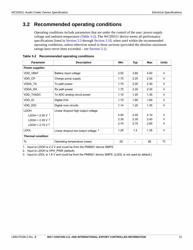
3.2 Recommended operating conditions
Operating conditions include parameters that are under the control of the user: power-supply voltage and ambient temperature (Table 3-2). The WCD9311 device meets all performance specifications listed in Section 3.3 through Section 3.10, when used within the recommended operating conditions, unless otherwise noted in those sections (provided the absolute maximum ratings have never been exceeded – see Section 3.1).
Table 3-2 Recommended operating conditions
Parameter Description Min Typ Max Units
Power supplies
VDD_VBAT Battery input voltage 2.50 3.80 4.50 V
VDD_CP Charge pump supply 1.70 2.20 2.30 V
VDDA_TX Tx path power 1.70 2.20 2.30 V
VDDA_RX Rx path power 1.70 2.20 2.30 V
VDD_TXADC Tx ADC analog circuit power 1.10 1.20 1.35 V
VDD_IO Digital I/Os 1.70 1.80 1.90 V
VDD_DIG Digital core circuits 1.14 1.20 1.35 V
LDOH
LDOH = 2.05 V11
LDOH = 2.35 V22
LDOH = 2.75 V 2
Linear dropout high output voltage
2.00
2.30
2.70
2.05
2.35
2.75
2.10
2.40
2.80
V
V
V
LDOL Linear dropout low output voltage33 1.25 1.3 1.35 V
Thermal condition
Tc Operating temperature (case) -30 – 85 ºC
1. Input to LDOH is 2.2 V and could be from the PM8921 device SMPS. 2. Input to LDOH is VPH_PWR (default). 3. Input to LDOL is 1.8 V and could be from the PM8921 device SMPS. (LDOL is not used by default.)
0598-3 Rev. B MAY CONTAIN U.S. AND INTERNATIONAL EXPORT CONTROLLED INFORMATION 23

LM80-P
WCD9311 Audio Codec Device Specification Electrical Specifications
3.3 DC power characteristics
3.3.1 Peak current
Table 3-3 Power supply peak current
Parameter Comments Min Typ Max Units
VDD_VBATT – – 20 mA
VDD_CP – – 500 mA
VDDA_TX – – 20 mA
VDDA_RX – – 20 mA
VDD_TXADC – – 5 mA
VDD_IO – – 5 mA
VDD_DIG – – 5 mA
LDOH – – 20 mA
LDOL – – 5 mA
0598-3 Rev. B MAY CONTAIN U.S. AND INTERNATIONAL EXPORT CONTROLLED INFORMATION 24

WCD Electrical Specifications
LM80 25
3.3
Tabl
ical current (µA)
VD
D_A
(1
.2V
)
VD
D_D
IG_
IO
(1.8
V)
VD
D_D
IG
(1.2
V)
Tota
l p
ow
er2
2
(mW
)
Res 0.45 0.04 2.86 0.01
Stan 0.44 0.05 2.86 0.01
Ster
6.80 24.40 988.60 4.01
6.80 29.80 1077.20 7.76
Steroutp
3.00 40.00 640.00 3.47
Stermon
4.00 40.00 610.00 3.56
Dev 162.00 110.00 1120.00 5.21
159.00 110.00 1120.00 5.22
325.00 110.00 1210.00 5.84
323.00 130.00 1210.00 5.86
3.00 170.00 930.00 4.45
5.00 190.00 840.00 4.39
9311 Audio Codec Device Specification
-P0598-3 Rev. B MAY CONTAIN U.S. AND INTERNATIONAL EXPORT CONTROLLED INFORMATION
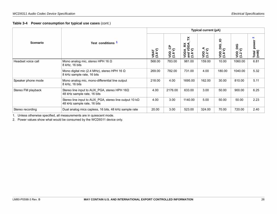
.2 Power consumption for typical use cases
e 3-4 Power consumption for typical use cases
Scenario Test conditions11
Typ
VB
AT
(3
.8V
)
VD
D_C
P
(1.8
V)
VD
DA
_RX
a
nd
VD
DA
_TX
(1
.8V
)
et WCD in reset (reset pin held high), MCLK off 1.80 0.05 0.16
dby (idle) WCD taken out of reset, MCLK off 1.80 0.05 0.16
eo playback to HPH 48 kHz, 16 bits, 16 Ω load, quiescent
48 kHz, 24 bits, 16 Ω load quiescent 1.40 812.40 726.60
48 kHz, 16 bits, 16 Ω load. 0.1 mW delivered to load
48 kHz, 24 bits, 16Ω load. 0.1 mW delivered to load 0.80 2810.60 744.60
eo playback to stereo line ut
48 kHz, 16 bits, 10 kΩ load
48 kHz, 24 bits, 10 kΩ load 4.00 4.00 1445.00
eo playback to o-differential line output
48 kHz, 16 bits, 10 kΩ load
48 kHz, 24 bits, 10 kΩ load 20.00 3.00 1483.00
ice voice call Analog mic, EAR PA 32 Ω, mono8 kHz sample rate, 16 bits
258.00 645.00 741.00
Analog mic, EAR PA 32 Ω, mono16 kHz sample rate, 16 bits
264.00 646.00 736.00
Stereo analog mics, EAR PA 32 Ω mono8 kHz sample rate, 16 bits
258.00 644.00 920.00
Stereo digital mics, EAR PA 32 Ω mono8 kHz sample rate, 16 bits
258.00 647.00 914.00
Digital mic (2.4 MHz), EAR PA 32 Ω, mono8 kHz, 16 bits
268.00 647.00 470.00
Digital mic (2.4 MHz), EAR PA 32Ω, mono16 kHz, 16 bits
268.00 647.00 470.00
WCD Electrical Specifications
LM80 26
Hea 159.00 10.00 1060.00 6.81
4.00 180.00 1040.00 5.32
Spe 162.00 30.00 810.00 5.11
Ster 3.00 50.00 900.00 6.25
5.00 50.00 50.00 2.23
Ster 324.00 70.00 720.00 2.40
1. U2. P
Tabl
ical current (µA)
VD
D_
A
(1.2
V)
VD
D_
DIG
_IO
(1
.8V
)
VD
D_
DIG
(1
.2V
)
Tota
l p
ow
er2
2
(mW
)
9311 Audio Codec Device Specification
-P0598-3 Rev. B MAY CONTAIN U.S. AND INTERNATIONAL EXPORT CONTROLLED INFORMATION
dset voice call Mono analog mic, stereo HPH 16 Ω8 kHz, 16 bits
568.00 783.00 981.00
Mono digital mic (2.4 MHz), stereo HPH 16 Ω8 kHz sample rate, 16 bits
269.00 782.00 731.00
aker phone mode Mono analog mic, mono-differential line output8 kHz, 16 bits
218.00 4.00 1695.00
eo FM playback Stereo line input to AUX_PGA, stereo HPH 16Ω48 kHz sample rate, 16 bits
4.00 2176.00 633.00
Stereo line input to AUX_PGA, stereo line output 10 kΩ48 kHz sample rate, 16 bits
4.00 3.00 1140.00
eo recording Dual analog mics capless, 16 bits, 48 kHz sample rate 20.00 3.00 523.00
nless otherwise specified, all measurements are in quiescent mode. ower values show what would be consumed by the WCD9311 device only.
e 3-4 Power consumption for typical use cases (cont.)
Scenario Test conditions11
Typ
VB
AT
(3
.8V
)
VD
D_
CP
(1
.8V
)
VD
DA
_R
X
and
VD
DA
_T
X
(1.8
V)

LM80-P
WCD9311 Audio Codec Device Specification Electrical Specifications
3.4 Powerup sequence
This information will be included in future revisions of this document.
3.5 Digital logic characteristics
3.6 Audio inputs and Tx processing
Unless otherwise stated, all Tx performance parameters are measured at the 48 kHz sampling rate.
3.6.1 Analog input through digital serial interface
Performance of the following Tx path is specified in Table 3-6: any analog input – pre-amp – ADC – digital serial interface.
Table 3-5 Digital I/O characteristics
Parameter Comments11 Min Typ Max Units
VIH High-level input voltage 0.65 · VDDX – 1.1 · VDDX V
VIL Low-level input voltage 0.10 · VDDX – 0.35 · VDDX V
VOH High-level output voltage 0.90 · VDDX – VDDX V
VOL Low-level output voltage 0 – 0.10 · VDDX V
CIN Digital input capacitance – – 5 pF
1. VDDX is the supply voltage associated with the digital I/O pin being tested (connected to the VDD_IO pin).
Table 3-6 Analog input through digital serial interface performance
Parameter Comments Min Typ Max Units
Microphone amplifier gain = 0 dB (minimum gain)
Input referred noise
Capless mode
Cap-coupled mode
Differential or single-ended; A-weightedVDDA_TX = 1.8 V or 2.2 V
VDDA_TX = 1.8 V or 2.2 V–
–
9.2
9.2
11.5
11.5
µVrms
µVrms
SNR
Differential input
Single-ended input
Capless or cap-coupled mode
VDDA_TX = 2.2 V
VDDA_TX = 1.8 V
VDDA_TX = 2.2 V
VDDA_TX = 1.8 V
99.0
93.0
93.0
90.0
102.0
96.0
96.0
93.0
–
–
–
–
dB
dB
dB
dB
THD + N ratio
Differential input
Differential or SE input
Capless or cap-coupled mode; VDDA_TX = 1.8 V or 2.2 V; f = 1.02 kHz; band-limited at 200 Hz to 20 kHz
Input level = -1 dBV
Input level = -60 dBV
86.0
34.0
91.0
41.0
–
–
dB
dB
0598-3 Rev. B MAY CONTAIN U.S. AND INTERNATIONAL EXPORT CONTROLLED INFORMATION 27

LM80-P
WCD9311 Audio Codec Device Specification Electrical Specifications
Microphone amplifier gain = 18 dB (maximum gain)
Input referred Noise
Capless mode
Cap-coupled mode
Differential or single-ended; A-weighted
VDDA_TX = 1.8 V or 2.2 V
VDDA_TX = 1.8 V or 2.2 V
–
–
4.4
3.7
5.6
5.0
µVrms
µVrms
SNR
Capless mode
Cap-coupled mode
Differential or single-ended input
VDDA_TX = 1.8 V or 2.2 V
VDDA_TX = 1.8 V or 2.2 V
87.0
88.0
89.0
90.0
–
–
dB
dB
THD + N ratio
Differential input
Differential or SE input
Capless or cap-coupled mode; VDDA_TX = 1.8 V or 2.2 V; f = 1.02 kHz; band-limited at 200 Hz to 20 kHz
Input level = -19 dBV
Input level = -60 dBV
70.0
23.0
78.0
29.0
–
–
dB
dB
Other characteristics
Full-scale input voltage Differential 1 kHz input. Input signal level required to get 0 dBFS digital output; VDDA_TX = 1.8 or 2.2 V capless or cap-coupled mode
-0.5 0 0.5 dBv
Absolute gain error -20 dBv input level, 1.02 kHz, VDDA_TX = 1.8 or 2.2 V
-0.5 – 0.5 dB
Power supply rejection
0 kHz < f < 1 kHz
1 kHz < f < 5 kHz
5 kHz < f < 2 0 kH
1.8 or 2.2 V analog; 100 mVpp square wave imposed on power supply; analog input = 0 Vrms
Terminated with 2 k; keep bypass caps on the pwr pin and measure 100 mV ripple at the pwr pin
51.0
51.0
51.0
56.0
56.0
56.0
–
–
–
dB
dB
dB
Input impedance
Cap-coupled, differential
Cap-coupled, single-ended
Capless
Input disabled
All gain modes
16.0
8.0
1.0
3.0
20.0
10.0
–
–
24.0
12.0
–
–
kk
MM
Input capacitance
Analog pin
Digital pin
Capless input mode
–
–
–
–
–
–
15
5
15
pF
pF
pF
Rx to Tx cross-talk attenuation
Tx path measurement with -5 dBFS Rx path signal. f = 1 kHz
90.0 100.0 – dB
Interchannel isolation 20 < f < 20 kHz; IN_1 terminated with 1 k; IN_2 = -5 dBFS at 1 kHz. Measure digital output of terminated channel.
90.0 100.0 – dB
Table 3-6 Analog input through digital serial interface performance (cont.)
Parameter Comments Min Typ Max Units
0598-3 Rev. B MAY CONTAIN U.S. AND INTERNATIONAL EXPORT CONTROLLED INFORMATION 28

LM80-P
WCD9311 Audio Codec Device Specification Electrical Specifications
Typical Tx path performance is shown in the following plots.
Figure 3-1 THD + N (0 dB gain)
Figure 3-2 THD + N (18 dB gain)
0
10
20
30
40
50
60
70
80
90
100
‐100 ‐80 ‐60 ‐40 ‐20 0
T
H
D
+
N(
d
B)
Input Level (dBv)
THD+N (0 dB gain)
Min
Typ
0
10
20
30
40
50
60
70
80
‐100 ‐80 ‐60 ‐40 ‐20 0
S
N
D
R
(
d
B)
Input Level (dBv)
THD+N (18 dB gain)
Min
Typ
0598-3 Rev. B MAY CONTAIN U.S. AND INTERNATIONAL EXPORT CONTROLLED INFORMATION 29

LM80-P
WCD9311 Audio Codec Device Specification Electrical Specifications
Figure 3-3 Frequency response (16 kHz)
Figure 3-4 Frequency response (48 kHz)
‐30
‐25
‐20
‐15
‐10
‐5
0
5
0 1000 2000 3000 4000 5000 6000 7000 8000 9000
A
m
p
l
i
t
u
d
e
(
d
B)
Frequency (Hz)
Frequency response 16kHz
Min
Max
‐30
‐25
‐20
‐15
‐10
‐5
0
5
0 5000 10000 15000 20000 25000 30000
A
m
p
l
i
t
u
d
e
(
d
B)
Frequency (Hz)
Frequency response 48kHz
Min
Max
0598-3 Rev. B MAY CONTAIN U.S. AND INTERNATIONAL EXPORT CONTROLLED INFORMATION 30

LM80-P
WCD9311 Audio Codec Device Specification Electrical Specifications
Figure 3-5 Frequency response (192 kHz)
‐30
‐25
‐20
‐15
‐10
‐5
0
5
0 20000 40000 60000 80000 100000 120000
A
m
p
l
i
t
u
d
e
(
d
B)
Frequency (dB)
Frequency response 192kHz
Min
Max
0598-3 Rev. B MAY CONTAIN U.S. AND INTERNATIONAL EXPORT CONTROLLED INFORMATION 31

LM80-P
WCD9311 Audio Codec Device Specification Electrical Specifications
3.6.2 DMIC input through digital serial interfacePerformance of the following Tx path is specified in Table 3-7: any digital microphone input – digital serial interface.
Table 3-7 Digital microphone input through digital serial interface performance
Parameter Comments Min Typ Max Units
16 kHz
SNR A-weighted 100.0 103.0 – dB
THD + N
PCM out = -1 dBFS
PCM out = -60 dBFS
f = 1.02 kHz; band-limited to 200 Hz – 1/2 * Fs
84.0
40.0
85.0
41.0
–
–
dB
dB
48 kHz
SNR PDM input 100.0 103.0 – dB
THD + N
PCM out = -1 dBFS
PCM out = -60 dBFS
f = 1.02 kHz; band-limited to 200 Hz – 1/2 * Fs
94.0
42.0
95.0
43.0
–
–
dB
dB
192 kHz
SNR PDM input, band-limited to 30 kHz – 1/2*Fs 39.0 40.0 – dB
THD + N
PCM out = -1 dBFS
PCM out = -60 dBFS
f = 50 kHz; band-limited to 30 kHz – 1/2*Fs
35.0
-16.0
36.0
-15.0
–
–
dB
dB
Other characteristics
Full-scale input signal
Decimator gain = 6 dB
Decimator gain = 0 dB
1 bit PDM; 1 kHz
–
–
75/25
100/0
–
–
%
%
Interchannel gain mismatch 1 kHz, -20 dBFS – 0.10 0.20 dB
Clock rate
MCLK = 9.6 MHz
MCLK = 12.288 MHz
MCLK = 24.576 MHz
Decimated output rates: 8 kHz, 16 kHz, 32 kHz, and 48 kHz, 192 kHz –
–
–
2.400
2.048
3.072
–
–
–
MHz
MHz
MHz
Clock duty cycle f = 1.024 MHz to 4.096 MHz 40/60 – 60/40 %
Input capacitance – 1.0 5.0 pF
Board capacitance – 10.0 50.0 pF
0598-3 Rev. B MAY CONTAIN U.S. AND INTERNATIONAL EXPORT CONTROLLED INFORMATION 32

LM80-P
WCD9311 Audio Codec Device Specification Electrical Specifications
ts
s
s
s
s
s
s
3.7 Audio outputs and Rx processing
Unless otherwise stated, all Rx performance parameters are measured at the 48 kHz sampling rate.
3.7.1 Digital serial interface through earpiece analog output
Performance of the following Rx path is specified in Table 3-8: digital serial input – mono DAC – mono EAR output.Out
Table 3-8 Serial interface through mono EAR output
Parameter Comments Min Typ Max Uni
EAR output; 8 kHz; 16 bits
Receive noise
6 dB gain (125 mW mode)
2 dB gain (50 mW mode)
A-weighted
–
–
9.5
6.7
12.0
9.0
µVrm
µVrm
SNR Ratio of full-scale output to output noise level, 2 or 6 dB gain
102.0 105.0 – dB
THD + N
PCMI = -1 dBFS
PCMI = -60 dBFS
Band-limited from 200 Hz to 20 kHz; 2 or 6 dB gain 68.0
32.0
72.0
38.0
–
–
dB
dB
EAR output; 48 kHz; 16 bits
Receive noise
6 dB gain (125 mW mode)
2 dB gain (50 mW mode)
A-weighted
–
–
9.5
6.7
12.0
9.0
µVrm
µVrm
SNR Ratio of full-scale output to output noise level, 2 or 6 dB gain
102.0 105.0 – dB
THD + N
PCMI = -1 dBFS
PCMI = -60 dBFS
Band-limited from 200 Hz to 20 kHz; 2 or 6 dB gain 84.0
34.0
89.5
38.0
–
–
dB
dB
EAR output; 48 or 192 kHz; 24 bits
Receive noise
6 dB gain (125 mW mode)
2 dB gain (50 mW mode)
A-weighted
–
–
9.5
6.7
12.0
9.0
µVrm
µVrm
SNR Ratio of full-scale output to output noise level, 2 or 6 dB gain
102.0 105.0 – dB
THD + N
PCMI = -1 dBFS
PCMI = -60 dBFS
Band-limited from 200 Hz to 20 kHz; 2 or 6 dB gain 83.0
41.0
89.0
47.0
–
–
dB
dB
0598-3 Rev. B MAY CONTAIN U.S. AND INTERNATIONAL EXPORT CONTROLLED INFORMATION 33

LM80-P
WCD9311 Audio Codec Device Specification Electrical Specifications
v
v
pp
ts
Other characteristics
Full-scale output voltage
6 dB PA gain mode
2 dB PA gain mode
PCMI = 0 dBFS, 1.02 kHz sine wave
5.5
1.6
6.0
2.1
6.5
2.6
dB
dB
Absolute gain error -20 dBFS input level, 1.02 kHz -0.5 – 0.5 dB
Output DC offset PCMI = -999 dBFs 1.0 3.0 mV
Output common mode voltage PCMI = -999 dBFs -0.05 0 0.05 V
Tx to Rx cross-talk attenuation Rx path measurement with -5 dBFS Tx path signal. f = 1 kHz
90.0 100.0 – dB
Power supply rejection
0 kHz < f < 1 kHz
1 kHz < f < 5 kHz
5 kHz < f < 20 kHz
100 mVpp squarewave imposed on power supply; digital input = -999 dBFS 80.0
70.0
70.0
85.0
80.0
75.0
–
–
–
dB
dB
dB
Disabled output impedance Measured externally with amplifier disabled 1 – – MΩ
Output capacitance Total capacitance between EAROP and EAROM, including PCB capacitance and EMI
– – 500 pF
Turn on/off click and pop level A-weighted; 10 k; 1 µF; 50 ms – -65.0 -58.0 dBV
Table 3-8 Serial interface through mono EAR output (cont.)
Parameter Comments Min Typ Max Uni
0598-3 Rev. B MAY CONTAIN U.S. AND INTERNATIONAL EXPORT CONTROLLED INFORMATION 34

LM80-P
WCD9311 Audio Codec Device Specification Electrical Specifications
Typical EAR path THD + N performance and a 16 kHz frequency response curve is shown in the following plots.
Figure 3-6 THD + N 8 kHz (EAR PA)
Figure 3-7 Frequency response 16 kHz (EAR PA)
0
10
20
30
40
50
60
70
80
90
100
‐120 ‐100 ‐80 ‐60 ‐40 ‐20 0
T
H
D
+
N
(
d
B)
Input level (dBFS)
THD+N 8 kHz (EAR PA)
Min
Typ
‐30
‐25
‐20
‐15
‐10
‐5
0
5
0 1000 2000 3000 4000 5000 6000 7000 8000 9000
A
m
p
l
i
t
u
d
e
(
d
B)
Frequency (Hz)
Frequency response 16 kHz (Ear PA)
Min
Max
0598-3 Rev. B MAY CONTAIN U.S. AND INTERNATIONAL EXPORT CONTROLLED INFORMATION 35

LM80-P
WCD9311 Audio Codec Device Specification Electrical Specifications
s
s
s
s
s
s
s
s
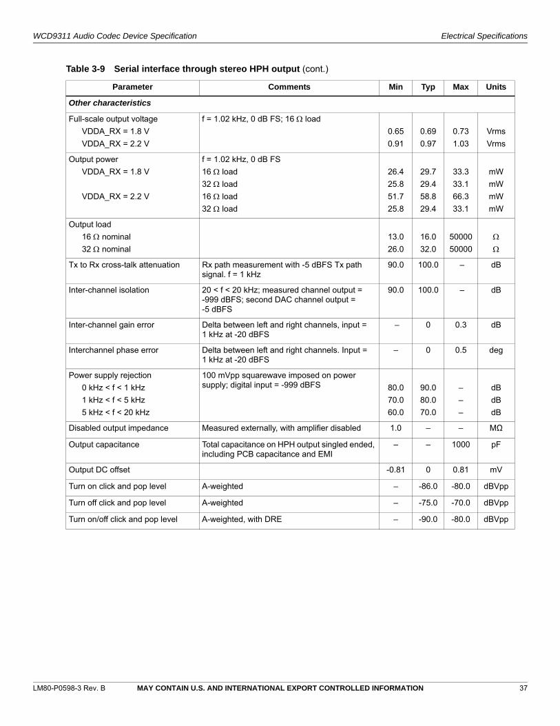
3.7.2 Digital serial interface through stereo HPH output
Performance of the following Rx path is specified in Table 3-9: digital serial input – stereo DAC – stereo HPH output.
Table 3-9 Serial interface through stereo HPH output
Parameter Comments Min Typ Max Units
HPH; 8 kHz; 16 bits
Receive noise
VDDA_RX = 1.8 V, no DRE
VDDA_RX = 2.2 V, no DRE
A-weighted; input = -999 dBFS
–
–
4.5
5.6
6.0
7.1
µVrm
µVrm
SNR
VDDA_RX = 1.8 V
VDDA_RX = 2.2 V
Ratio of full-scale output to output noise level
101.0
104.0
102.5
105.5
–
–
dB
dB
THD + N
PCMI = -1 dBFS
PCMI = -60 dBFS
Band-limited from 200 Hz to 20 kHz; VDDA_RX = 1.8 V or 2.2 V 68.0
36.0
72.0
38.0
–
–
dB
dB
HPH; 48 kHz; 16bits
Receive noise
VDDA_RX = 1.8 V, no DRE
VDDA_RX = 2.2 V, no DRE
VDDA_RX = 1.8 V or 2.2 V, DRE enabled
A-weighted; input = -999 dBFS
–
–
–
4.5
5.6
2.2
6.0
7.1
3.5
µVrm
µVrm
µVrm
SNR
VDDA = 1.8 V
VDDA = 2.2 V
Ratio of full-scale output to output noise level
101.0
104.0
102.5
105.5
–
–
dB
dB
THD + N
PCMI = -1 dBFS
PCMI = -60 dBFS
Band-limited from 200 Hz to 20 kHz; VDDA_RX = 1.8 V or 2.2 V 84.0
38.0
89.0
40.0
–
–
dB
dB
HPH; 48 or 192 kHz; 24 bits
Receive noise
VDDA_RX = 1.8 V, no DRE
VDDA_RX = 2.2 V, no DRE
VDDA_RX = 1.8 V or 2.2 V, DRE enabled
A-weighted; input = -999 dBFS
–
–
–
4.5
5.6
2.2
6.0
7.1
3.5
µVrm
µVrm
µVrm
SNR
VDDA = 1.8 V, no DRE
VDDA = 2.2 V, no DRE
VDDA_RX = 1.8 V, with DRE
VDDA_RX = 2.2 V, with DRE
Ratio of full-scale output to output noise level; A-weighted 101.0
104.4
106.0
109.0
102.5
105.5
108.0
111.0
–
–
–
–
dB
dB
dB
dB
THD + N
PCMI = -1 dBFS
PCMI = -60 dBFS
Band-limited from 200 Hz to 20 kHz;
VDDA_RX = 1.8 V
VDDA_RX = 1.8, A-weighted
84.0
38.0
89.0
44.0
–
–
dB
dB
0598-3 Rev. B MAY CONTAIN U.S. AND INTERNATIONAL EXPORT CONTROLLED INFORMATION 36
LM80-P
WCD9311 Audio Codec Device Specification Electrical Specifications
p
p
p
Other characteristics
Full-scale output voltage
VDDA_RX = 1.8 V
VDDA_RX = 2.2 V
f = 1.02 kHz, 0 dB FS; 16 load
0.65
0.91
0.69
0.97
0.73
1.03
Vrms
Vrms
Output power
VDDA_RX = 1.8 V
VDDA_RX = 2.2 V
f = 1.02 kHz, 0 dB FS
16 load
32 load
16 load
32 load
26.4
25.8
51.7
25.8
29.7
29.4
58.8
29.4
33.3
33.1
66.3
33.1
mW
mW
mW
mW
Output load
16 nominal
32 nominal
13.0
26.0
16.0
32.0
50000
50000
Tx to Rx cross-talk attenuation Rx path measurement with -5 dBFS Tx path signal. f = 1 kHz
90.0 100.0 – dB
Inter-channel isolation 20 < f < 20 kHz; measured channel output = -999 dBFS; second DAC channel output = -5 dBFS
90.0 100.0 – dB
Inter-channel gain error Delta between left and right channels, input = 1 kHz at -20 dBFS
– 0 0.3 dB
Interchannel phase error Delta between left and right channels. Input = 1 kHz at -20 dBFS
– 0 0.5 deg
Power supply rejection
0 kHz < f < 1 kHz
1 kHz < f < 5 kHz
5 kHz < f < 20 kHz
100 mVpp squarewave imposed on power supply; digital input = -999 dBFS 80.0
70.0
60.0
90.0
80.0
70.0
–
–
–
dB
dB
dB
Disabled output impedance Measured externally, with amplifier disabled 1.0 – – MΩ
Output capacitance Total capacitance on HPH output singled ended, including PCB capacitance and EMI
– – 1000 pF
Output DC offset -0.81 0 0.81 mV
Turn on click and pop level A-weighted – -86.0 -80.0 dBVp
Turn off click and pop level A-weighted – -75.0 -70.0 dBVp
Turn on/off click and pop level A-weighted, with DRE – -90.0 -80.0 dBVp
Table 3-9 Serial interface through stereo HPH output (cont.)
Parameter Comments Min Typ Max Units
0598-3 Rev. B MAY CONTAIN U.S. AND INTERNATIONAL EXPORT CONTROLLED INFORMATION 37

LM80-P
WCD9311 Audio Codec Device Specification Electrical Specifications
Typical HPH path THD + N performance and a 48 kHz frequency response curve is shown in the following plots.
.
Figure 3-8 THD + N 48 kHz (HPH PA)
Figure 3-9 Frequency response 48 kHz (HPH PA)
0
10
20
30
40
50
60
70
80
90
100
‐120 ‐100 ‐80 ‐60 ‐40 ‐20 0
T
H
D
+
N(
d
B)
Input level (dBFS)
THD+N 48 kHz (HPH PA)
Min
Typ
‐30
‐25
‐20
‐15
‐10
‐5
0
5
0 5000 10000 15000 20000 25000 30000
A
m
p
l
i
t
u
d
e
(
d
B)
Frequency (Hz)
Frequency response 48 kHz (HPH PA)
Min
Max
0598-3 Rev. B MAY CONTAIN U.S. AND INTERNATIONAL EXPORT CONTROLLED INFORMATION 38
LM80-P
WCD9311 Audio Codec Device Specification Electrical Specifications
s
s
s
s
s
s
s
s
s
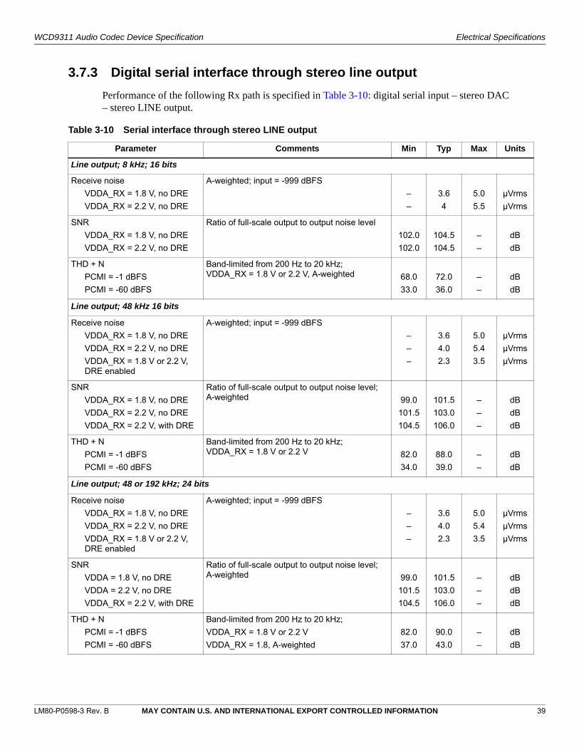
3.7.3 Digital serial interface through stereo line output
Performance of the following Rx path is specified in Table 3-10: digital serial input – stereo DAC – stereo LINE output.
Table 3-10 Serial interface through stereo LINE output
Parameter Comments Min Typ Max Unit
Line output; 8 kHz; 16 bits
Receive noise
VDDA_RX = 1.8 V, no DRE
VDDA_RX = 2.2 V, no DRE
A-weighted; input = -999 dBFS
–
–
3.6
4
5.0
5.5
µVrm
µVrm
SNR
VDDA_RX = 1.8 V, no DRE
VDDA_RX = 2.2 V, no DRE
Ratio of full-scale output to output noise level
102.0
102.0
104.5
104.5
–
–
dB
dB
THD + N
PCMI = -1 dBFS
PCMI = -60 dBFS
Band-limited from 200 Hz to 20 kHz; VDDA_RX = 1.8 V or 2.2 V, A-weighted 68.0
33.0
72.0
36.0
–
–
dB
dB
Line output; 48 kHz 16 bits
Receive noise
VDDA_RX = 1.8 V, no DRE
VDDA_RX = 2.2 V, no DRE
VDDA_RX = 1.8 V or 2.2 V, DRE enabled
A-weighted; input = -999 dBFS
–
–
–
3.6
4.0
2.3
5.0
5.4
3.5
µVrm
µVrm
µVrm
SNR
VDDA_RX = 1.8 V, no DRE
VDDA_RX = 2.2 V, no DRE
VDDA_RX = 2.2 V, with DRE
Ratio of full-scale output to output noise level; A-weighted 99.0
101.5
104.5
101.5
103.0
106.0
–
–
–
dB
dB
dB
THD + N
PCMI = -1 dBFS
PCMI = -60 dBFS
Band-limited from 200 Hz to 20 kHz; VDDA_RX = 1.8 V or 2.2 V 82.0
34.0
88.0
39.0
–
–
dB
dB
Line output; 48 or 192 kHz; 24 bits
Receive noise
VDDA_RX = 1.8 V, no DRE
VDDA_RX = 2.2 V, no DRE
VDDA_RX = 1.8 V or 2.2 V, DRE enabled
A-weighted; input = -999 dBFS
–
–
–
3.6
4.0
2.3
5.0
5.4
3.5
µVrm
µVrm
µVrm
SNR
VDDA = 1.8 V, no DRE
VDDA = 2.2 V, no DRE
VDDA_RX = 2.2 V, with DRE
Ratio of full-scale output to output noise level; A-weighted 99.0
101.5
104.5
101.5
103.0
106.0
–
–
–
dB
dB
dB
THD + N
PCMI = -1 dBFS
PCMI = -60 dBFS
Band-limited from 200 Hz to 20 kHz;
VDDA_RX = 1.8 V or 2.2 V
VDDA_RX = 1.8, A-weighted
82.0
37.0
90.0
43.0
–
–
dB
dB
0598-3 Rev. B MAY CONTAIN U.S. AND INTERNATIONAL EXPORT CONTROLLED INFORMATION 39

LM80-P
WCD9311 Audio Codec Device Specification Electrical Specifications
s
s
p
p
s
Other characteristics
Full-scale output voltage
VDDA_RX = 1.8 V
VDDA_RX = 2.2 V
f = 1.02 kHz, 0 dB FS; 600 load
0.47
0.56
0.50
0.60
0.53
0.63
Vrm
Vrm
Output common mode voltage
VDDA_RX = 1.8 V
VDDA_RX = 2.2 V
PCMI = -999 dBFs
0.80
1.00
0.85
1.05
0.90
1.10
V
V
Output load Single ended – 600 1 M Ω
Tx to Rx cross-talk attenuation Rx path measurement with -5 dBFS Tx path signal. f = 1 kHz
90.0 100.0 – dB
Inter-channel isolation 20 < f < 20 kHz; measured channel output = -999 dBFS; AUXPGA or second DAC channel output = -5 dBFS
90.0 100.0 – dB
Power supply rejection
0 kHz < f < 1 kHz
1 kHz < f < 5 kHz
5 kHz < f < 20 kHz
100 mVpp squarewave imposed on power supply; digital input = -999 dBFS; VDDA_RX = 2.2 V or 1.8 V analog
80.0
70.0
70.0
85.0
80.0
75.0
–
–
–
dB
dB
dB
Output impedance
PA disabled
PA enabled
Measured externally, with amplifier disabled
20 to 20 kHz bandwidth
1
–
–
–
–
10.0
M
Output capacitance Total capacitance on LINE output singled ended, including PCB capacitance and EMI
– – 1000 pF
Turn on click and pop level A-weighted; 10 k ohms; 1 µF; 50 ms – -56.0 -55.0 dBVp
Turn off click and pop level A-weighted; 10 k ohms; 1 µF; 50 ms – -61.0 -55.0 dBVp
Table 3-10 Serial interface through stereo LINE output (cont.)
Parameter Comments Min Typ Max Unit
0598-3 Rev. B MAY CONTAIN U.S. AND INTERNATIONAL EXPORT CONTROLLED INFORMATION 40

LM80-P
WCD9311 Audio Codec Device Specification Electrical Specifications
ts
s
s
s
s
s
s
s
s
3.7.4 Digital serial interface through mono-differential line outputs
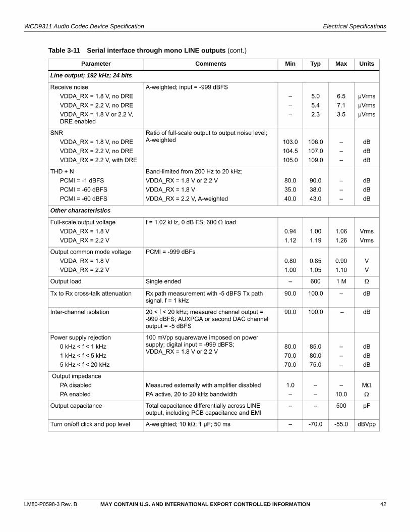
Performance of the following Rx path is specified in Table 3-11: digital serial input – mono DAC – mono-differential LINE outputs.
Table 3-11 Serial interface through mono LINE outputs
Parameter Comments Min Typ Max Uni
Line output; 8 kHz 16 bits
Receive noise
VDDA_RX = 1.8 V, no DRE
VDDA_RX = 2.2 V, no DRE
A-weighted; input = -999 dBFS
–
–
5.0
5.4
6.5
7.1
µVrm
µVrm
SNR
VDDA_RX = 1.8 V, no DRE
VDDA_RX = 2.2 V, no DRE
VDDA_RX = 2.2 V, with DRE
Ratio of full-scale output to output noise level
103.0
104.5
105.0
106.0
107.0
108.0
–
–
–
dB
dB
dB
THD + N
PCMI = -1 dBFS
PCMI = -60 dBFS
Band-limited from 200 Hz to 20 kHz; VDDA_RX = 1.8 V or 2.2 V, A-weighted 68.0
36.0
72.0
39.0
–
–
dB
dB
Line output; 48 kHz 16 bits
Receive noise
VDDA_RX = 1.8 V, no DRE
VDDA_RX = 2.2 V, no DRE
VDDA_RX = 1.8 V or 2.2 V, DRE enabled
A-weighted; input = -999 dBFS
–
–
–
5.0
5.4
2.3
6.5
7.1
3.5
µVrm
µVrm
µVrm
SNR
VDDA_RX = 1.8 V, no DRE
VDDA_RX = 2.2 V, no DRE
VDDA_RX = 2.2 V, with DRE
Ratio of full-scale output to output noise level; A-weighted 103.0
104.5
105.0
106.0
107.0
108.0
–
–
–
dB
dB
dB
THD + N
PCMI = -1 dBFS
PCMI = -60 dBFS
Band-limited from 200 Hz to 20 kHz; VDDA_RX = 1.8 V or 2.2 V 91.0
33.0
97.0
39.0
–
–
dB
dB
Line output; 48 kHz; 24 bits
Receive noise
VDDA_RX = 1.8 V, no DRE
VDDA_RX = 2.2 V, no DRE
VDDA_RX = 1.8 V or 2.2 V, DRE enabled
A-weighted; input = -999 dBFS
–
–
–
5.0
5.4
2.3
6.5
7.1
3.5
µVrm
µVrm
µVrm
SNR
VDDA_RX = 1.8 V, no DRE
VDDA_RX = 2.2 V, no DRE
VDDA_RX = 2.2 V, with DRE
Ratio of full-scale output to output noise level;A-weighted 103.0
104.5
105.0
106.0
107.0
108.0
–
–
–
dB
dB
dB
THD + N
PCMI = -1 dBFS
PCMI = -60 dBFS
Band-limited from 200 Hz to 20 kHz;
VDDA_RX = 1.8 V or 2.2 V
VDDA_RX = 1.8, A-weighted
91.0
33.0
97.0
39.0
–
–
dB
dB
0598-3 Rev. B MAY CONTAIN U.S. AND INTERNATIONAL EXPORT CONTROLLED INFORMATION 41
LM80-P
WCD9311 Audio Codec Device Specification Electrical Specifications
s
s
s
s
s
pp
ts
Line output; 192 kHz; 24 bits
Receive noise
VDDA_RX = 1.8 V, no DRE
VDDA_RX = 2.2 V, no DRE
VDDA_RX = 1.8 V or 2.2 V, DRE enabled
A-weighted; input = -999 dBFS
–
–
–
5.0
5.4
2.3
6.5
7.1
3.5
µVrm
µVrm
µVrm
SNR
VDDA_RX = 1.8 V, no DRE
VDDA_RX = 2.2 V, no DRE
VDDA_RX = 2.2 V, with DRE
Ratio of full-scale output to output noise level; A-weighted 103.0
104.5
105.0
106.0
107.0
109.0
–
–
–
dB
dB
dB
THD + N
PCMI = -1 dBFS
PCMI = -60 dBFS
PCMI = -60 dBFS
Band-limited from 200 Hz to 20 kHz;
VDDA_RX = 1.8 V or 2.2 V
VDDA_RX = 1.8 V
VDDA_RX = 2.2 V, A-weighted
80.0
35.0
40.0
90.0
38.0
43.0
–
–
–
dB
dB
dB
Other characteristics
Full-scale output voltage
VDDA_RX = 1.8 V
VDDA_RX = 2.2 V
f = 1.02 kHz, 0 dB FS; 600 load
0.94
1.12
1.00
1.19
1.06
1.26
Vrm
Vrm
Output common mode voltage
VDDA_RX = 1.8 V
VDDA_RX = 2.2 V
PCMI = -999 dBFs
0.80
1.00
0.85
1.05
0.90
1.10
V
V
Output load Single ended – 600 1 M Ω
Tx to Rx cross-talk attenuation Rx path measurement with -5 dBFS Tx path signal. f = 1 kHz
90.0 100.0 – dB
Inter-channel isolation 20 < f < 20 kHz; measured channel output = -999 dBFS; AUXPGA or second DAC channel output = -5 dBFS
90.0 100.0 – dB
Power supply rejection
0 kHz < f < 1 kHz
1 kHz < f < 5 kHz
5 kHz < f < 20 kHz
100 mVpp squarewave imposed on power supply; digital input = -999 dBFS; VDDA_RX = 1.8 V or 2.2 V
80.0
70.0
70.0
85.0
80.0
75.0
–
–
–
dB
dB
dB
Output impedance
PA disabled
PA enabled
Measured externally with amplifier disabled
PA active, 20 to 20 kHz bandwidth
1.0
–
–
–
–
10.0
M
Output capacitance Total capacitance differentially across LINE output, including PCB capacitance and EMI
– – 500 pF
Turn on/off click and pop level A-weighted; 10 k; 1 µF; 50 ms – -70.0 -55.0 dBV
Table 3-11 Serial interface through mono LINE outputs (cont.)
Parameter Comments Min Typ Max Uni
0598-3 Rev. B MAY CONTAIN U.S. AND INTERNATIONAL EXPORT CONTROLLED INFORMATION 42

LM80-P
WCD9311 Audio Codec Device Specification Electrical Specifications
Typical single-ended LINE path THD + N performance and a 192 kHz frequency response curve is shown in the following plots.
Figure 3-10 THD + N 192 kHz (LINE_OUT PA)
Figure 3-11 Frequency response 192 kHz (LINE_OUT PA)
0
10
20
30
40
50
60
70
80
90
100
‐120 ‐100 ‐80 ‐60 ‐40 ‐20 0
T
H
D
+
N
(
d
B)
Input level (dBFS)
THD+N 192 kHz(LINE_OUT PA)
Min
Typ
‐30
‐25
‐20
‐15
‐10
‐5
0
5
0 20000 40000 60000 80000 100000 120000
A
m
p
l
i
t
u
d
e
d
B
Frequency (Hz)
Frequency response 192 kHz (LINE_OUT PA)
Min
Max
0598-3 Rev. B MAY CONTAIN U.S. AND INTERNATIONAL EXPORT CONTROLLED INFORMATION 43
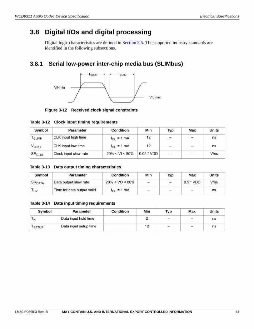
LM80-P
WCD9311 Audio Codec Device Specification Electrical Specifications
3.8 Digital I/Os and digital processing
Digital logic characteristics are defined in Section 3.5. The supported industry standards are identified in the following subsections.
3.8.1 Serial low-power inter-chip media bus (SLIMbus)
Figure 3-12 Received clock signal constraints
Table 3-12 Clock input timing requirements
Symbol Parameter Condition Min Typ Max Units
TCLKIH CLK input high time IOL = 1 mA 12 – – ns
VCLKIL CLK input low time IOH = 1 mA 12 – – ns
SRCLKI Clock input slew rate 20% < VI < 80% 0.02 * VDD – – V/ns
Table 3-13 Data output timing characteristics
Symbol Parameter Condition Min Typ Max Units
SRDATA Data output slew rate 20% < VO < 80% – – 0.5 * VDD V/ns
TDV Time for data output valid IOH = 1 mA – – – ns
Table 3-14 Data input timing requirements
Symbol Parameter Condition Min Typ Max Units
TH Data input hold time 2 – – ns
TSETUP Data input setup time 12 – – ns
0598-3 Rev. B MAY CONTAIN U.S. AND INTERNATIONAL EXPORT CONTROLLED INFORMATION 44
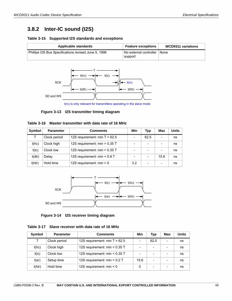
LM80-P
WCD9311 Audio Codec Device Specification Electrical Specifications
3.8.2 Inter-IC sound (I2S)
Figure 3-13 I2S transmitter timing diagram
Figure 3-14 I2S receiver timing diagram
Table 3-15 Supported I2S standards and exceptions
Applicable standards Feature exceptions WCD9311 variations
Phillips I2S Bus Specifications revised June 5, 1996 No external controller support
None
t(rc)SCK
SD and WS
T
t(lc)t(hc)
t(dtr) t(htr)
t(rc) is only relevant for transmitters operating in the slave mode
Table 3-16 Master transmitter with data rate of 16 MHz
Symbol Parameter Comments Min Typ Max Units
T Clock period 12S requirement: min T = 62.5 - 62.5 - ns
t(hc) Clock high 12S requirement: min > 0.35 T - - - ns
t(lc) Clock low 12S requirement: min > 0.35 T - - - ns
t(dtr) Delay 12S requirement: min < 0.8 T - - 15.6 ns
t(htr) Hold time 12S requirement: min > 0 3.2 - - ns
SCK
SD and WS
T
t(lc) t(hc)
t(htr)t(sr)
Table 3-17 Slave receiver with data rate of 16 MHz
Symbol Parameter Comments Min Typ Max Units
T Clock period 12S requirement: min T = 62.5 - 62.5 - ns
t(hc) Clock high 12S requirement: min < 0.35 T - - - ns
t(lc) Clock low 12S requirement: min < 0.35 T - - - ns
t(sr) Setup time 12S requirement: min < 0.2 T 15.6 - - ns
t(htr) Hold time 12S requirement: min < 0 0 - - ns
0598-3 Rev. B MAY CONTAIN U.S. AND INTERNATIONAL EXPORT CONTROLLED INFORMATION 45

LM80-P
WCD9311 Audio Codec Device Specification Electrical Specifications
3.8.3 Interintegrated circuit (I2C)
3.8.4 Digital MIC PDM interface
Figure 3-15 WCD9311 received clock signal constraints
Table 3-18 Supported I2C standards and exceptions
Applicable standards Feature exceptions WCD9311 variations
I2C Specification, version 2.1, January 2000 None
VsSel
WCD9311clkData2
VsSel
clkData1
Dmic L
Dmic R Select (Sel) Mode
GND
Vs
Left (Data2)
Right (Data1)
Mbias
0.1uF
0.1uF
Internal Signal
DMIC 2
DMIC 1
GND
Vs
Left (Data6)
Right (Data5)
DMIC 6
DMIC 5
GND
Vs
Left (Data4)
Right (Data3)
DMIC 4
DMIC 3
Clk0 / Clk1 / Clk2
Data1 / Data3 / Data5
Data2 / Data4 /Data6 data
data
t2
t1
t2
t1
Table 3-19 Digital microphone timing
Parameter Comments Min Typ Max Units
T1 5 15 25 ns
T2 20 35 50 ns
0598-3 Rev. B MAY CONTAIN U.S. AND INTERNATIONAL EXPORT CONTROLLED INFORMATION 46

LM80-P
WCD9311 Audio Codec Device Specification Electrical Specifications
3.9 Support circuits – analog
3.9.1 Microphone bias
Table 3-20 Microphone bias performance
Parameter Comments Min Typ Max Units
Output voltage
Normal operation
MBHC calibration
3 mA microphone load
No noise filtering in this mode
1.70
0.20
–
–
2.85
1.50
V
V
Output current Two microphone loads of 1 to 1.5 mA each – – 3.0 mA
Microphone bias current consumption
– 80 150 µA
Output switch to ground
On resistance
Sink current
–
2.0
–
–
20
–
mA
Output noise 0.1 µF bypass 0.5 2.0 3.0 µVrms
Power supply rejection ratio
at 20 Hz
200 Hz to 1 kHz
at 5 kHz
at 10 kHz
at 20 kHz
100 mVpp applied to VDD_VBATT input
93
113
100
90
78
–
–
–
–
–
–
–
–
–
–
dB
dB
dB
dB
dB
Intermicrophone isolation DC current = 50 µA, 2.2 k bias resistor; 20 Hz to 80 kHz
70 – – dB
Noise filtering cap at CFILT pin – 0.1 – µF
Load capacitance
With load cap mode
No external cap mode
0
–
0.1
–
0.5
270
μF
pF
0598-3 Rev. B MAY CONTAIN U.S. AND INTERNATIONAL EXPORT CONTROLLED INFORMATION 47

LM80-P
WCD9311 Audio Codec Device Specification Electrical Specifications
s
s
s
3.9.2 Analog input through AUX_PGA
Performance of the following Tx path is specified in Table 3-21: analog input – AUX_PGA – power amplifier output.
3.10 Support circuits – digital
Digital logic characteristics are defined in Section 3.5; additional performance specifications are not required.
Table 3-21 Analog input to AUX_PGA to output PA specifications
Parameter Comments Min Typ Max Unit
AUX PGA end to end
SNR
Ear amp
HPH amp
Line amp
Differential, gain = 0 dB, A-weightedInput = 1.02 kHz, -60 dBV 101.0
100.0
97.0
104.0
103.0
100.0
–
–
–
dB
dB
dB
THD + N ratio
Ear amp
HPH amp
Line amp
Input = 1.02 kHz -13 dBv SE, gain = 12 dB
Differential
Single-ended
Single-ended
80.0
80.0
80.0
–
–
–
–
–
–
dB
dB
Max. input voltage
Differential
Single-ended
f = 1.02 kHz
0.94
0.47
1.00
0.50
1.06
0.53
Vrm
Vrm
Gain error Input = 1.02 kHz, 0.5 dBv, differential -0.5 – 0.5 dB
Frequency response 20 Hz to 20 kHz, input signal level = -20 dBv; applies to all paths, gain = 0 dB
-0.5 – 0.5 dB
0598-3 Rev. B MAY CONTAIN U.S. AND INTERNATIONAL EXPORT CONTROLLED INFORMATION 48

LM80-P
4 Mechanical Information
4.1 Device physical dimensions
The WCD9311 device is available in the 86 pin CSP that includes dedicated ground pins for improved grounding, mechanical strength, and thermal continuity. The 86 pin CSP has a 6.0 by 6.0 mm body with a maximum height of 1.27 mm. Pin A1 is located by an indicator mark on the top of the package. A simplified version of the 86 pin CSP outline drawing is shown in Figure 4-1.
0598-3 Rev. B MAY CONTAIN U.S. AND INTERNATIONAL EXPORT CONTROLLED INFORMATION 49.
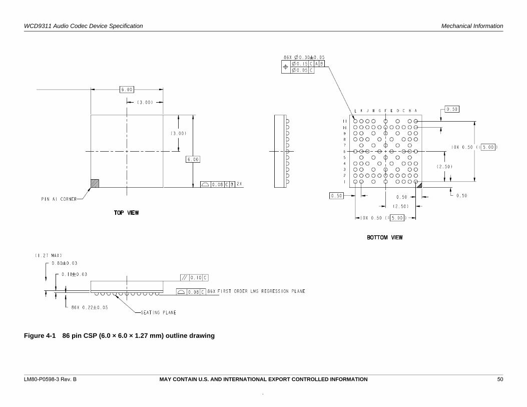
WCD Mechanical Information
LM80 50
Figu
9311 Audio Codec Device Specification
-P0598-3 Rev. B MAY CONTAIN U.S. AND INTERNATIONAL EXPORT CONTROLLED INFORMATION
.
re 4-1 86 pin CSP (6.0 × 6.0 × 1.27 mm) outline drawing
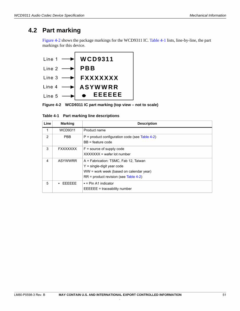
LM80-P
WCD9311 Audio Codec Device Specification Mechanical Information
4.2 Part marking
Figure 4-2 shows the package markings for the WCD9311 IC. Table 4-1 lists, line-by-line, the part markings for this device.
Figure 4-2 WCD9311 IC part marking (top view – not to scale)
Table 4-1 Part marking line descriptions
Line Marking Description
1 WCD9311 Product name
2 PBB P = product configuration code (see Table 4-2)
BB = feature code
3 FXXXXXXX F = source of supply code
XXXXXXX = wafer lot number
4 ASYWWRR A = Fabrication: TSMC, Fab 12, Taiwan
Y = single-digit year code
WW = work week (based on calendar year)
RR = product revision (see Table 4-2)
5 • EEEEEE • = Pin A1 indicator
EEEEEE = traceability number
Line 1
FXXXXXXX
Line 2
Line 3
Line 5
PBB
W CD9311
Line 4 ASYW W RREEEEEE
0598-3 Rev. B MAY CONTAIN U.S. AND INTERNATIONAL EXPORT CONTROLLED INFORMATION 51.

LM80-P
WCD9311 Audio Codec Device Specification Mechanical Information
4.3 Device ordering information
This device can be ordered using the identification code shown in Figure 4-3; the device ID code is explained in the following text.
Figure 4-3 WDC9311 device identification code
An example for the WCD9311 device can be as follows: WCD9311-0-86CSP-TR-02-0.
Device ordering information details for all samples available to date are summarized in Table 4-2.
DDCCCBBB RRPAAA-AAAA
RR: Product revision(ex. RR = 02)
AAA-AAAA: Product name
(ex: WCD-9311)
P: Configuration code(ex. P = 0)
BBB: Number of pins (ex. 86)
DD: Packing information (DD="TR"= tape and reel)
S
CCC: Package type(ex. CSP)
S: Source code(ex. S = 0)
Table 4-2 Device identification code/ordering information details
PM variant Product configuration code (P) Product revision (RR) HW ID # S value11
ES1 sample type
WCD9311 0 02 – 0
1. S is the source configuration code that identifies all the qualified die fabrication source combinations available at the time a particular sample type was shipped. S values are defined in Table 4-3.
Table 4-3 Source configuration code
S value F value = A F value = B F value = C
0 TSMC – –
0598-3 Rev. B MAY CONTAIN U.S. AND INTERNATIONAL EXPORT CONTROLLED INFORMATION 52.

LM80-P
WCD9311 Audio Codec Device Specification Mechanical Information
4.4 Device moisture-sensitivity level
The CSP devices are susceptible to damage induced by absorbed moisture and high temperature. The latest revision IPC/JEDEC J-STD-020 standard revision for moisture-sensitivity qualification is followed. WCD9311 devices are classified as MSL1@260ºC. This is the MSL classification temperature, which is defined as the minimum temperature moisture-sensitivity testing during device qualification.
Additional MSL information is included in other sections of this document or in other documents:
Section 5.2.1 – Storage
Section 5.2.3 – Handling
Section 7.1 – Reliability qualifications summary
4.5 Thermal characteristics
The WCD9311 device in its 86 pin CSP has the typical thermal resistance listed in Table 4-4.
Table 4-4 Device thermal resistance
Parameter Comment Typical Units
JA Thermal resistance, J-to-A Junction-to-ambient (still air)11
1. Junction-to-ambient thermal resistance (JA) is calculated based upon the maximum die junction temperature and the total package power dissipation; ambient temperature is 85°C.
40 °C/W
JC Thermal resistance, J-to-C Junction-to-case22
2. Junction-to-case thermal resistance (JC) applies to situations in which nearly all the heat flows out the top of the package.
0.82 °C/W
0598-3 Rev. B MAY CONTAIN U.S. AND INTERNATIONAL EXPORT CONTROLLED INFORMATION 53.
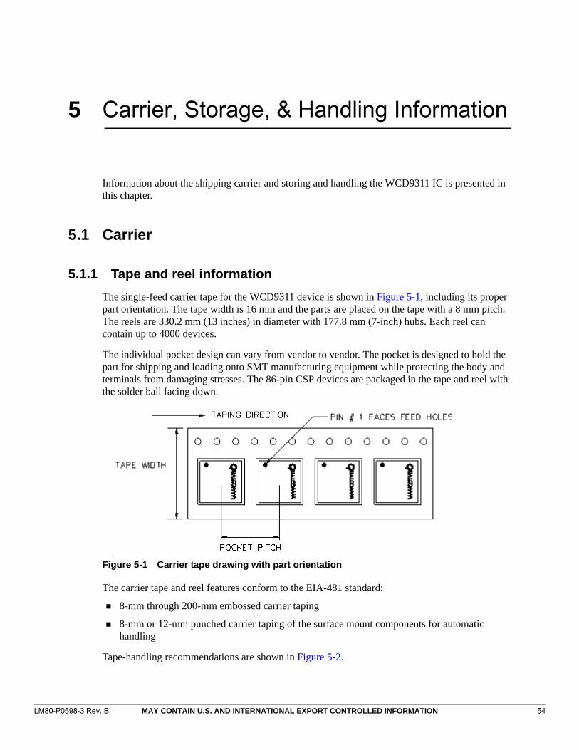
LM80-P
5 Carrier, Storage, & Handling Information
Information about the shipping carrier and storing and handling the WCD9311 IC is presented in this chapter.
5.1 Carrier
5.1.1 Tape and reel information
The single-feed carrier tape for the WCD9311 device is shown in Figure 5-1, including its proper part orientation. The tape width is 16 mm and the parts are placed on the tape with a 8 mm pitch. The reels are 330.2 mm (13 inches) in diameter with 177.8 mm (7-inch) hubs. Each reel can contain up to 4000 devices.
The individual pocket design can vary from vendor to vendor. The pocket is designed to hold the part for shipping and loading onto SMT manufacturing equipment while protecting the body and terminals from damaging stresses. The 86-pin CSP devices are packaged in the tape and reel with the solder ball facing down.
Figure 5-1 Carrier tape drawing with part orientation
The carrier tape and reel features conform to the EIA-481 standard:
8-mm through 200-mm embossed carrier taping
8-mm or 12-mm punched carrier taping of the surface mount components for automatic handling
Tape-handling recommendations are shown in Figure 5-2.
0598-3 Rev. B MAY CONTAIN U.S. AND INTERNATIONAL EXPORT CONTROLLED INFORMATION 54
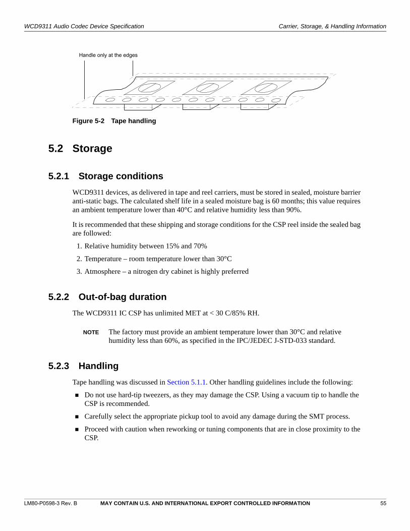
LM80-P
WCD9311 Audio Codec Device Specification Carrier, Storage, & Handling Information
Figure 5-2 Tape handling
5.2 Storage
5.2.1 Storage conditions
WCD9311 devices, as delivered in tape and reel carriers, must be stored in sealed, moisture barrier anti-static bags. The calculated shelf life in a sealed moisture bag is 60 months; this value requires an ambient temperature lower than 40°C and relative humidity less than 90%.
It is recommended that these shipping and storage conditions for the CSP reel inside the sealed bag are followed:
1. Relative humidity between 15% and 70%
2. Temperature – room temperature lower than 30°C
3. Atmosphere – a nitrogen dry cabinet is highly preferred
5.2.2 Out-of-bag duration
The WCD9311 IC CSP has unlimited MET at < 30 C/85% RH.
NOTE The factory must provide an ambient temperature lower than 30°C and relative humidity less than 60%, as specified in the IPC/JEDEC J-STD-033 standard.
5.2.3 Handling
Tape handling was discussed in Section 5.1.1. Other handling guidelines include the following:
Do not use hard-tip tweezers, as they may damage the CSP. Using a vacuum tip to handle the CSP is recommended.
Carefully select the appropriate pickup tool to avoid any damage during the SMT process.
Proceed with caution when reworking or tuning components that are in close proximity to the CSP.
Handle only at the edges
0598-3 Rev. B MAY CONTAIN U.S. AND INTERNATIONAL EXPORT CONTROLLED INFORMATION 55

LM80-P
WCD9311 Audio Codec Device Specification Carrier, Storage, & Handling Information
5.2.4 Baking
It is not necessary to bake the WCD9311 devices.
5.2.5 Electrostatic discharge
Electrostatic discharge (ESD) occurs naturally in laboratory and factory environments. An established high-voltage potential is always at risk of discharging to a lower potential. If this discharge path is through a semiconductor device, destructive damage could result.
ESD countermeasures and handling methods must be developed and used to control the factory environment at each manufacturing site.
Products must be handled according to the ESD Association standard, ANSI/ESD S20.20-2007, Protection of Electrical and Electronic Parts, Assemblies, and Equipment.
Refer to Chapter 7 for the WCD9311 device ESD ratings.
0598-3 Rev. B MAY CONTAIN U.S. AND INTERNATIONAL EXPORT CONTROLLED INFORMATION 56
LM80-P
6 PCB Mounting Guidelines
6.1 Land pad and stencil design
The land pattern and stencil recommendations presented in this section are based upon internal characterizations using lead-free solder pastes on an eight-layer test PCB, and a 100 micron-thick stencil. The PCB land pattern and stencil design for the 86 pin CSP is the same whether SnPb or lead-free solder is used.
6.2 SMT development and characterization
The information presented in this section describes board-level characterization process parameters. It is included to assist customers when starting their SMT process development; it is not intended as specifications for customer SMT processes.
NOTE It is recommended that customers follow their solder-paste vendor recommendations for the screen-printing process parameters and reflow profile conditions.
Characterization tests attempt to optimize the SMT process for the best board-level reliability possible. This is done by performing physical tests on evaluation boards. The tests may include the following:
Peel test
Bend-to-failure
Bend cycle
Tensile pull
Drop shock
Temperature cycling
It is recommended to characterize the land patterns according to each customer's processes, materials, equipment, stencil design, and reflow profile prior to PCB production. Review the land pattern and stencil design recommendations in Section 6.1 as a guide for characterization.
Optimizing the solder stencil pattern design and print process is critical to ensuring print uniformity, decreasing voiding, and increasing board-level reliability.
Any particular underfill products are not endorsed.
0598-3 Rev. B MAY CONTAIN U.S. AND INTERNATIONAL EXPORT CONTROLLED INFORMATION 57

LM80-P
WCD9311 Audio Codec Device Specification PCB Mounting Guidelines
Reflow profile conditions typically used for SnPb and lead-free systems are given in Table 6-1.
6.3 SMT peak package-body temperature
Factory floor-life prior to solder-attach is addressed within Section 5.2.2 (Out-of-bag duration).
The following limits during the SMT board-level solder attach process are recommended:
SMT peak package body temperature of 245°C – the temperature that must not be exceeded as measured on the package body’s top surface
Maximum duration of 40 to 70 seconds at this temperature
Although the solder paste manufacturer’s recommendations for optimum temperature and duration for solder reflow must be followed, the recommended limits must not be exceeded.
6.4 SMT process verification
Verification of the SMT process prior to high-volume PCB fabrication is recommended, including:
Electrical continuity
X-ray inspection of the package installation for proper alignment, solder voids, solder balls, and solder bridging
Visual inspection
Cross-section inspection of solder joints to confirm registration, fillet shape, and print volume (insufficient, acceptable, or excessive)
Table 6-1 Typical SMT reflow profile conditions (for reference only)
Profile stage DescriptionLead-free (high-temp)
condition limits
Preheat Initial ramp < 3°C/sec max
Soak Dry out and flux activation 150 to 190°C
60 to 120 sec
Reflow Time above solder paste melting point 40 to 70 sec
SMT peak package-body temperature 245°C
Cool down Cool rate – ramp-to-ambient 6°C/sec max
0598-3 Rev. B MAY CONTAIN U.S. AND INTERNATIONAL EXPORT CONTROLLED INFORMATION 58

LM80-P
7 Part Reliability
7.1 Reliability qualification summary
Table 7-1 Reliability evaluation summary
Tests, standards, and conditions Sample Size Result
Average failure rate (AFR) in FIT () failure in billion device-hours:
HTOL: JESD22-A108-A
Use condition: temperature: Tj = 70°C, VDD nominal
569 30 FIT
Mean time to failure (MTTF) t = 1/ in million hours 569 33 million hrs
ESD – human-body model (HBM) rating:
JESD22-A114-D
3
2000 V
ESD – charge-device model (CDM) rating
JESD22-C101-C
3
500 V
Latch-up (I-test): EIA/JESD78:
Trigger current: ±100 mA; temperature: 85C6
Pass
Latch-up (Vsupply overvoltage): EIA/JESD78
Trigger voltage: 1.5 x Vnom V; temperature: 85C6 Pass
Moisture resistance test (MRT): J-STD-020 E
Reflow at 260 +0/-5 C480
MSL 1
Temperature cycle: JESD22-A104-C
Temperature: -55 to 125C; number of cycles: 1000
Soak time at min/max temperature: 2 minutes
Cycle rate: 2 cycles per hour (cph)
Preconditioning: JESD22-A113-E
MSL: 1, reflow temperature: 260 +0/-5C
240 Pass
Unbiased highly accelerated stress test (UHAST):
JESD22-A118-B
Preconditioning: JESD22-A113-E
MSL: 1, reflow temperature: 260 +0/-5C
240 Pass
High temperature storage life: JESD22-A103-C
Temperature 150C, 1000 hours
90 Pass
Die shear: MIL-STD-883E, Method 2019 15 Pass
Solder ball shear: JESD22-B117 120 Pass
Solder bump shear 60 Pass
0598-3 Rev. B MAY CONTAIN U.S. AND INTERNATIONAL EXPORT CONTROLLED INFORMATION 59
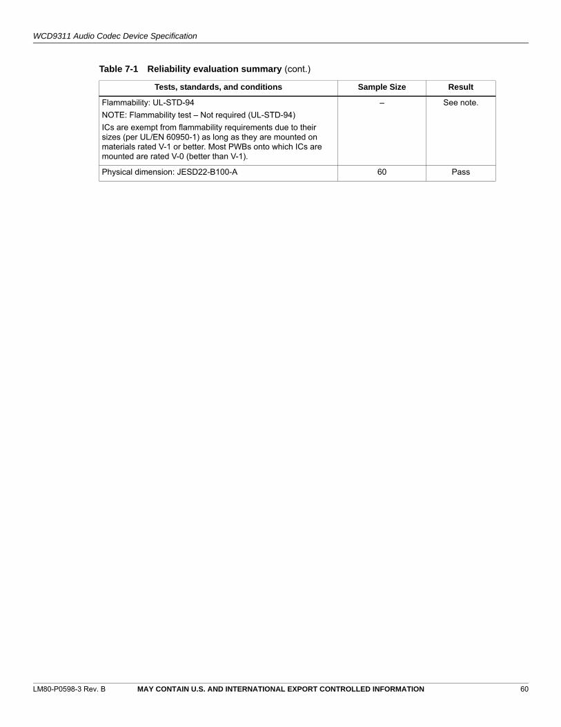
LM80-P
WCD9311 Audio Codec Device Specification
Flammability: UL-STD-94
NOTE: Flammability test – Not required (UL-STD-94)
ICs are exempt from flammability requirements due to their sizes (per UL/EN 60950-1) as long as they are mounted on materials rated V-1 or better. Most PWBs onto which ICs are mounted are rated V-0 (better than V-1).
– See note.
Physical dimension: JESD22-B100-A 60 Pass
Table 7-1 Reliability evaluation summary (cont.)
Tests, standards, and conditions Sample Size Result
0598-3 Rev. B MAY CONTAIN U.S. AND INTERNATIONAL EXPORT CONTROLLED INFORMATION 60

LM80-P
A Terms and Acronyms
A1.1 Terms and acronyms
Table A1-1 defines terms and acronyms commonly used throughout this document.
Table A1-1 Terms and acronyms
Term Definition
ADC Analog-to-digital converter
ANC Active noise cancellation
APQ Application-only processor
bps Bits per second
CDM Charged-device model
CMOS Complementary metal oxide semiconductor
CP Charge pump
CSP Chip-scale package
DAC Digital-to-analog converter
DMIC Digital microphone
DNC Do not connect
DRE Dynamic range enhancement
ESD Electrostatic discharge
FM Frequency modulation
HBM Human-body model
HPH Headphone
IC Integrated circuit
I2C Inter-integrated circuit
I2S Inter-IC sound
I/O Input/output
IIR Infinite impulse response
kbps Kilobits per second
LDO Low dropout (linear regulator)
MBHC Multibutton headset control
MIC Microphone
0598-3 Rev. B MAY CONTAIN U.S. AND INTERNATIONAL EXPORT CONTROLLED INFORMATION 61

LM80-P
WCD9311 Audio Codec Device Specification Terms and Acronyms
S
MSBit or MSByte Defines whether the MSB is the most significant bit or most significant byte. All instances of MSB used in this manual are assumed to be MSByte, unless otherwise specified.
NS Nano second
OEM Original equipment manufacturer
PA Power amplifier
PCB Printed circuit board
PCM Pulse-coded modulation
PGA Programmable gain amplifier
PM Power management
RH Relative humidity
RoHS Restriction of hazardous substances
Rx Receive, receiver
SE Single-ended
SLIMbus Serial low-power inter-chip media bus
SMT Surface-mount technology
SNR Signal-to-noise ratio
Tx Transmit, transmitter
WCD WSP coder/decoder
WSP Wafer-scale package
Table A1-1 Terms and acronyms (cont.)
Term Definition
0598-3 Rev. B MAY CONTAIN U.S. AND INTERNATIONAL EXPORT CONTROLLED INFORMATION 62

LM80-P
B Exhibit 1
1. PLEASE READ THIS LICENSE AGREEMENT (“AGREEMENT”) CAREFULLY. THIS AGREEMENT IS A BINDING LEGAL AGREEMENT ENTERED INTO BY AND BETWEEN YOU (OR IF YOU ARE ENTERING INTO THIS AGREEMENT ON BEHALF OF AN ENTITY, THEN THE ENTITY THAT YOU REPRESENT) AND QUALCOMM TECHNOLOGIES, INC. (“QTI” “WE” “OUR” OR “US”). THIS IS THE AGREEMENT THAT APPLIES TO YOUR USE OF THE DESIGNATED AND/OR ATTACHED DOCUMENTATION AND ANY UPDATES OR IMPROVEMENTS THEREOF (COLLECTIVELY, “MATERIALS”). BY USING OR COMPLETING THE INSTALLATION OF THE MATERIALS, YOU ARE ACCEPTING THIS AGREEMENT AND YOU AGREE TO BE BOUND BY ITS TERMS AND CONDITIONS. IF YOU DO NOT AGREE TO THESE TERMS, QTI IS UNWILLING TO AND DOES NOT LICENSE THE MATERIALS TO YOU. IF YOU DO NOT AGREE TO THESE TERMS YOU MUST DISCONTINUE AND YOU MAY NOT USE THE MATERIALS OR RETAIN ANY COPIES OF THE MATERIALS. ANY USE OR POSSESSION OF THE MATERIALS BY YOU IS SUBJECT TO THE TERMS AND CONDITIONS SET FORTH IN THIS AGREEMENT.
License. Subject to the terms and conditions of this Agreement, including, without limitation, the restrictions, conditions, limitations and exclusions set forth in this Agreement, Qualcomm Technologies, Inc. (“QTI”) hereby grants to you a nonexclusive, limited license under QTI’s copyrights to use the attached Materials; and to reproduce and redistribute a reasonable number of copies of the Materials. You may not use Qualcomm Technologies or its affiliates or subsidiaries name, logo or trademarks; and copyright, trademark, patent and any other notices that appear on the Materials may not be removed or obscured. QTI shall be free to use suggestions, feedback or other informationreceived from You, without obligation of any kind to You. QTI may immediately terminate this Agreement upon your breach. Upon termination of this Agreement, Sections 1.2-4 shall survive.
Indemnification. You agree to indemnify and hold harmless QTI and its officers, directors, employees and successors and assigns against any and all third party claims, demands, causes of action, losses, liabilities, damages, costs and expenses, incurred by QTI (including but not limited to costs of defense, investigation and reasonable attorney’s fees) arising out of, resulting from or related to: (i) any breach of this Agreement by You; and (ii) your acts, omissions, products and services. If requested by QTI, You agree to defend QTI in connection with any third party claims, demands, or causes of action resulting from, arising out of or in connection with any of the foregoing.
Ownership. QTI (or its licensors) shall retain title and all ownership rights in and to the Materials and all copies thereof, and nothing herein shall be deemed to grant any right to You under any of QTI's or its affiliates’ patents. You shall not subject the Materials to any third party license terms (e.g., open source license terms). You shall not use the Materials for the purpose of identifying or providing evidence to support any potential patent infringement claim against QTI, its affiliates, or any of QTI’s or QTI’s affiliates’ suppliers and/or direct or indirect customers. QTI hereby reserves all rights not expressly granted herein.
WARRANTY DISCLAIMER. YOU EXPRESSLY ACKNOWLEDGE AND AGREE THAT THE USE OF THE MATERIALS IS AT YOUR SOLE RISK. THE MATERIALS AND TECHNICAL SUPPORT, IF ANY, ARE PROVIDED “AS IS” AND WITHOUT WARRANTY OF ANY KIND, WHETHER EXPRESS OR IMPLIED. QTI ITS LICENSORS AND AFFILIATES MAKE NO WARRANTIES, EXPRESS OR IMPLIED, WITH RESPECT TO THE MATERIALS OR ANY OTHER INFORMATION OR DOCUMENTATION PROVIDED UNDER THIS AGREEMENT, INCLUDING BUT NOT LIMITED TO ANY WARRANTY OF MERCHANTABILITY OR FITNESS FOR A PARTICULAR PURPOSE OR AGAINST INFRINGEMENT, OR ANY EXPRESS OR IMPLIED WARRANTY ARISING OUT OF TRADE USAGE OR OUT OF A COURSE OF DEALING OR COURSE OF PERFORMANCE. NOTHING CONTAINED IN THIS AGREEMENT SHALL BE CONSTRUED AS (I) A WARRANTY OR REPRESENTATION BY QTI, ITS LICENSORS OR AFFILIATES AS TO THE VALIDITY OR SCOPE OF ANY PATENT, COPYRIGHT OR OTHER INTELLECTUAL PROPERTY RIGHT OR (II) A WARRANTY OR REPRESENTATION BY QTI THAT ANY MANUFACTURE OR USE WILL BE FREE FROM INFRINGEMENT OF PATENTS, COPYRIGHTS OR OTHER INTELLECTUAL PROPERTY RIGHTS OF OTHERS, AND IT SHALL BE THE SOLE RESPONSIBILITY OF YOU TO MAKE SUCH DETERMINATION AS IS NECESSARY WITH RESPECT TO THE ACQUISITION OF LICENSES UNDER PATENTS AND OTHER INTELLECTUAL PROPERTY OF THIRD PARTIES.
LIMITATION OF LIABILITY. IN NO EVENT SHALL QTI, QTI’S AFFILIATES OR ITS LICENSORS BE LIABLE TO YOU FOR ANY INCIDENTAL, CONSEQUENTIAL OR SPECIAL DAMAGES, INCLUDING BUT NOT LIMITED TO ANY LOST PROFITS, LOST SAVINGS, OR OTHER INCIDENTAL DAMAGES, ARISING OUT OF THE USE OR INABILITY TO USE, OR THE DELIVERY OR FAILURE TO DELIVER, ANY OF THE MATERIALS, OR ANY BREACH OF ANY OBLIGATION UNDER THIS AGREEMENT, EVEN IF QTI HAS BEEN ADVISED OF THE POSSIBILITY OF SUCH DAMAGES. THE FOREGOING LIMITATION OF LIABILITY SHALL REMAIN IN FULL FORCE AND EFFECT REGARDLESS OF WHETHER YOUR REMEDIES HEREUNDER ARE DETERMINED TO HAVE FAILED OF THEIR ESSENTIAL PURPOSE. THE ENTIRE LIABILITY OF QTI, QTI’s AFFILIATES AND ITS LICENSORS, AND THE SOLE AND EXCLUSIVE REMEDY OF YOU, FOR ANY CLAIM OR CAUSE OF ACTION ARISING HEREUNDER (WHETHER IN CONTRACT, TORT, OR OTHERWISE) SHALL NOT EXCEED US$10.2. COMPLIANCE WITH LAWS; APPLICABLE LAW. You agree to comply with all applicable local, international and national laws and regulations and with U.S. Export Administration Regulations, as they apply to the subject matter of this Agreement. This Agreement is governed by the laws of the State of California, excluding California’s choice of law rules.
3. CONTRACTING PARTIES. If the Materials are downloaded on any computer owned by a corporation or other legal entity, then thisAgreement is formed by and between QTI and such entity. The individual accepting the terms of this Agreement represents and warrants to QTIthat they have the authority to bind such entity to the terms and conditions of this Agreement.
4. MISCELLANEOUS PROVISIONS. This Agreement, together with all exhibits attached hereto, which are incorporated herein bythis reference, constitutes the entire agreement between QTI and You and supersedes all prior negotiations, representations and agreementsbetween the parties with respect to the subject matter hereof. No addition or modification of this Agreement shall be effective unless made inwriting and signed by the respective representatives of QTI and You. The restrictions, limitations, exclusions and conditions set forth in thisAgreement shall apply even if QTI or any of its affiliates becomes aware of or fails to act in a manner to address any violation or failure tocomply therewith. You hereby acknowledge and agree that the restrictions, limitations, conditions and exclusions imposed in this Agreement on
0598-3 Rev. B MAY CONTAIN U.S. AND INTERNATIONAL EXPORT CONTROLLED INFORMATION 63

LM80-P
WCD9311 Audio Codec Device Specification Exhibit 1
the rights granted in this Agreement are not a derogation of the benefits of such rights. You further acknowledges that, in the absence of suchrestrictions, limitations, conditions and exclusions, QTI would not have entered into this Agreement with You. Each party shall be responsiblefor and shall bear its own expenses in connection with this Agreement. If any of the provisions of this Agreement are determined to be invalid,illegal, or otherwise unenforceable, the remaining provisions shall remain in full force and effect. This Agreement is entered into solely in theEnglish language, and if for any reason any other language version is prepared by any party, it shall be solely for convenience and the Englishversion shall govern and control all aspects. If You are located in the province of Quebec, Canada, the following applies: The Parties herebyconfirm they have requested this Agreement and all related documents be prepared in English.
0598-3 Rev. B MAY CONTAIN U.S. AND INTERNATIONAL EXPORT CONTROLLED INFORMATION 64