wavelength selective mode division multiplexing on a …people.sutd.edu.sg/ricky_ang/oe2015.pdf ·...
TRANSCRIPT
Wavelength selective mode division multiplexing on a silicon chip
G. F. R. Chen,1 T. Wang,1 K. J. A. Ooi,1 A. K. L. Chee,2 L. K. Ang1 and D. T. H. Tan1,* 1Singapore University of Technology and Design, 8 Somapah Rd., Singapore 487372, Singapore
2Massachusetts Institute of Technology, 77 Massachusetts Ave. Cambridge MA 02139, USA *[email protected],
Abstract: Multiplexing of optical modes in waveguides is demonstrated using coupled vertical gratings. The device utilizes sinusoidally corrugated waveguides of different widths with a period designed to multiplex information at 1.55µm. The design, fabrication and characterization of devices is performed. Multiplexing of modes is demonstrated in optical structures which support 3 and 5 quasi-TE modes. The design utilizes counter-propagating modes in periodic structures, thus enabling the device to combine its mode division multiplexing capabilities with wavelength division multiplexing functionalities to further augment the multiplexing capacity of the device.
©2015 Optical Society of America
OCIS codes: (130.2790) Guided waves; (130.3120) Integrated optics devices; (130.7408) Wavelength filtering devices.
References and links
1. R. S. Tucker, G. Eisenstein, and S. K. Korotky, “Optical time-division multiplexing for very high bit-rate transmission,” J. Lightwave Technol. 6(11), 1737–1749 (1988).
2. S. Kawanishi, “Ultrahigh-speed optical time-division-multiplexed transmission technology based on optical signal processing,” IEEE J. Quantum Electron. 34(11), 2064–2079 (1998).
3. D. T. H. Tan, K. Ikeda, S. Zamek, A. Mizrahi, M. P. Nezhad, A. V. Krishnamoorthy, K. Raj, J. E. Cunningham, X. Zheng, I. Shubin, Y. Luo, and Y. Fainman, “Wide bandwidth, low loss 1 by 4 wavelength division multiplexer on silicon for optical interconnects,” Opt. Express 19(3), 2401–2409 (2011).
4. D. T. H. Tan, A. Grieco, and Y. Fainman, “Towards 100 channel dense wavelength division multiplexing with 100GHz spacing on silicon,” Opt. Express 22(9), 10408–10415 (2014).
5. F. Xia, M. O'Boyle, L. Sekaric, and Y. Vlasov, ” Ultra-Compact Wavelength Division Multiplexing Devices Using Silicon Photonic Wires for On-Chip Interconnects,” in Optical Fiber Communication Conference and Exposition and The National Fiber Optic Engineers Conference, OSA Technical Digest Series (CD) (Optical Society of America, 2007), paper OWG2.
6. C. P. Chen, J. Driscoll, B. Souhan, R. Grote, X. Zhu, R. M. Osgood, and K. Bergman, “Experimental Demonstration of Spatial Scaling for High-Throughput Transmission Through A Si Mode-Division-Multiplexing Waveguide,” in Advanced Photonics for Communications, OSA Technical Digest (online) (Optical Society of America, 2014), paper IM2A.3.
7. L.-W. Luo, N. Ophir, C. P. Chen, L. H. Gabrielli, C. B. Poitras, K. Bergmen, and M. Lipson, “WDM-compatible mode-division multiplexing on a silicon chip,” Nat. Commun. 5, 3069 (2014).
8. J. Wang, S. He, and D. Dai, “On-chip silicon 8-channel hybrid (de)multiplexer enabling simultaneous mode- and polarization-division- multiplexing,” Laser and Photonics Reviews. 8(2), L18–L22 (2014).
9. H. Qiu, H. Yu, T. Hu, G. Jiang, H. Shao, P. Yu, J. Yang, and X. Jiang, “Silicon mode multi/demultiplexer based on multimode grating-assisted couplers,” Opt. Express 21(15), 17904–17911 (2013).
10. S. G. Evangelides, L. F. Mollenauer, J. P. Gordon, and N. S. Bergano, “Polarization multiplexing with solitons,” J. Lightwave Technol. 10(1), 28–35 (1992).
11. X. S. Yao, L.-S. Yan, B. Zhang, A. E. Willner, and J. Jiang, “All-optic scheme for automatic polarization division demultiplexing,” Opt. Express 15(12), 7407–7414 (2007).
12. N. Bozinovic, Y. Yue, Y. Ren, M. Tur, P. Kristensen, H. Huang, A. E. Willner, and S. Ramachandran, “Terabit-scale orbital angular momentum mode division multiplexing in fibers,” Science 340(6140), 1545–1548 (2013).
13. B. Guan, R. P. Scott, C. Qin, N. K. Fontaine, T. Su, C. Ferrari, M. Cappuzzo, F. Klemens, B. Keller, M. Earnshaw, and S. J. Yoo, “Free-space coherent optical communication with orbital angular, momentum multiplexing/demultiplexing using a hybrid 3D photonic integrated circuit,” Opt. Express 22(1), 145–156 (2014).
14. D. T. H. Tan, K. Ikeda, and Y. Fainman, “Coupled chirped vertical gratings for on chip group velocity dispersion engineering,” Appl. Phys. Lett. 95(14), 141109 (2009).
#231690 - $15.00 USD Received 5 Jan 2015; revised 9 Mar 2015; accepted 11 Mar 2015; published 20 Mar 2015 © 2015 OSA 23 Mar 2015 | Vol. 23, No. 6 | DOI:10.1364/OE.23.008095 | OPTICS EXPRESS 8095
15. D. T. H. Tan, K. Ikeda, R. E. Saperstein, B. Slutsky, and Y. Fainman, “Chip-scale dispersion engineering using chirped vertical gratings,” Opt. Lett. 33(24), 3013–3015 (2008).
16. G. F. R. Chen, T. Wang, C. Donnelly, and D. T. H. Tan, “Second and third order dispersion generation using nonlinearly chirped silicon waveguide gratings,” Opt. Express 21(24), 29223–29230 (2013).
17. D. T. H. Tan, P. C. Sun, and Y. Fainman, “Monolithic nonlinear pulse compressor on a silicon chip,” Nat. Commun. 1(8), 116 (2010).
18. W. Shi, H. Yun, C. Lin, J. Flueckiger, N. A. F. Jaeger, and L. Chrostowski, “Coupler-apodized Bragg-grating add-drop filter,” Opt. Lett. 38(16), 3068–3070 (2013).
19. D. T. H. Tan, “Optical pulse compression on a silicon chip – Effect of group velocity dispersion and free carriers,” Appl. Phys. Lett. 101(21), 211112 (2012).
20. A. Yariv and P. Yeh, Optical Waves in Crystals: Propagation and Control of Laser Radiation (Wiley, 1984). 21. W. Shi, H. Yun, C. Lin, M. Greenberg, X. Wang, Y. Wang, S. T. Fard, J. Flueckiger, N. A. F. Jaeger, and L.
Chrostowski, “Ultra-compact, flat-top demultiplexer using anti-reflection contra-directional couplers for CWDM networks on silicon,” Opt. Express 21(6), 6733–6738 (2013).
1. Introduction
Multiplexing of information is a commonly used technique to increase the data capacity of a transmission medium. This may be done in the time domain [1,2], wavelength [3–5], mode [6–9], polarization [10,11] and most recently, angular orbital momentum [12,13]. In optical time division multiplexing, optical pulses are interleaved in time, and therefore the data capacity scales inversely with the pulse width. Wavelength division multiplexing enables data channels to be supported at different wavelengths. Modal division multiplexing however, operates based on the orthogonality of waveguide modes. Different modes co-propagating in a waveguide cannot couple to one another and therefore, a multi-mode waveguide may be used to increase the amount of data carried by utilizing each mode as a separate channel. With the increasing need for short reach interconnects to provide greater bandwidth and reduce power consumption in microprocessors and data centers, the management of on-chip data is important.
In this paper, we investigate the use of coupled gratings [14–18] for mode division multiplexing on a chip. We have previously demonstrated the use of such coupled gratings for use in dispersion engineering [14–16], pulse compression [17] and wavelength division multiplexing [3,4]. Contrary to closely spaced adjacent waveguides where coupling occurs in co-propagating modes, periodic perturbations introduced to two coupled waveguides provides a mechanism for cross-coupling of modes to occur contra-directionally [20]. Consequently, the fundamental mode of a single mode waveguide grating may be used to couple into an adjacent multi-mode waveguide grating at the wavelength of interest, via proper selection of the corrugation period. The use of waveguide gratings supporting three and four modes for mode-division multiplexing on a chip is studied for operation at 1.55µm. The design, fabrication and characterization of these devices are performed.
2. Design
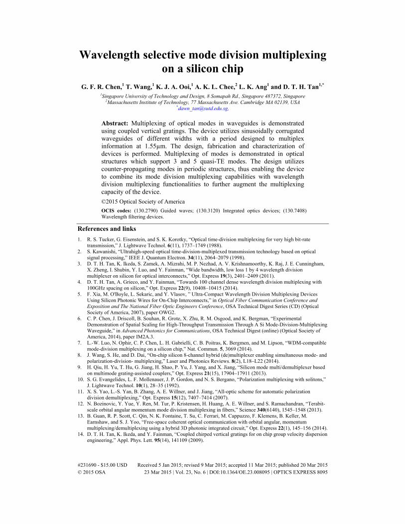
Figure 1(a) shows the schematic of a MDM device based on coupled vertical gratings. The left grating is based on a single mode waveguide, and has a modulation depth of 50nm. The right grating is a multi-mode waveguide, with width, W1 = 450nm, W2 = 1250nm or 1850nm, each supporting three and five modes respectively. An apodization filter is also applied to eliminate unwanted side lobes in the spectra. The device length, L is fixed at 500µm and the gap, G between the two coupled gratings is 80nm or 100nm. A larger value of G leads to a smaller overlap integral between the modes in the two coupled gratings and a smaller coupling coefficient overall [2,17]. The cross coupling Bragg condition governing the drop wavelength is given by,
c eff1 eff2,m.( )n nλ = Λ + (Eq. 1)
Or equivalently,
#231690 - $15.00 USD Received 5 Jan 2015; revised 9 Mar 2015; accepted 11 Mar 2015; published 20 Mar 2015 © 2015 OSA 23 Mar 2015 | Vol. 23, No. 6 | DOI:10.1364/OE.23.008095 | OPTICS EXPRESS 8096
1 2
2πβ β+ =Λ
(Eq. 2)
where neff1 and neff2,m are the effective indices of the modes in the right and left waveguide gratings respectively. β1 and β2 are the propagation constants of the right and left waveguide gratings respectively. In wavelength division multiplexing previously demonstrated, neff,1 and neff2,m are simply that of the fundamental modes in each grating (m = 0). In this case, neff1 represents the effective index of right waveguide’s fundamental mode, and neff2,m represents the effective index of the mth order in the multi-mode waveguide on the left. In this particular device, the introduction of the periodic perturbation creates a wavelength selectivity which can be combined with mode division multiplexing to achieve two different methods of multiplexing simultaneously. Figure 1(c) shows a device schematic of how the wavelength selectivity can be combined with mode division multiplexing to achieve this.
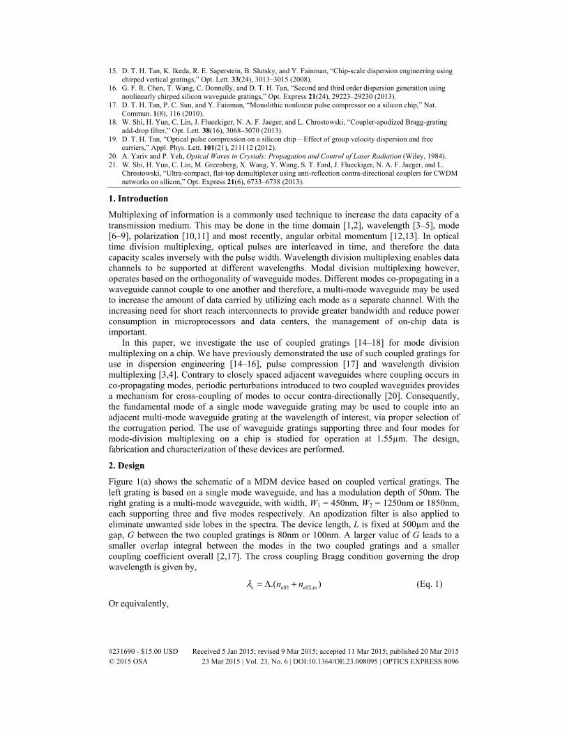
Fig. 1. (a) Device schematic for the mode division multiplexer. The MDM consists of two coupled gratings with widths, W1 and W2 respectively and modulation depths of ∆W1 and ∆W2 respectively. The peak to peak separation between W1 and W2 is denoted by the gap width, G. (b) SEM micrograph over two periods of a typical device showing a close up of the gap. (c) Schematic of how the MDM device can be combined with wavelength division multiplexing capabilities.
#231690 - $15.00 USD Received 5 Jan 2015; revised 9 Mar 2015; accepted 11 Mar 2015; published 20 Mar 2015 © 2015 OSA 23 Mar 2015 | Vol. 23, No. 6 | DOI:10.1364/OE.23.008095 | OPTICS EXPRESS 8097
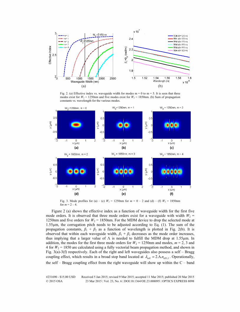
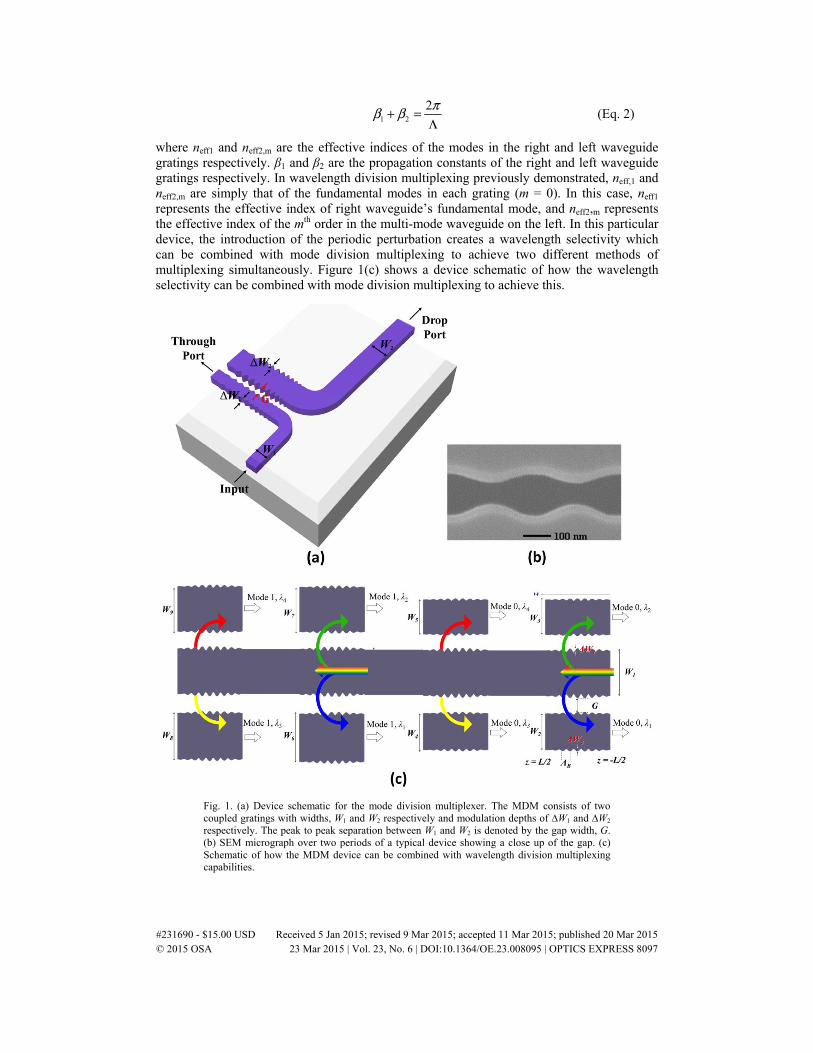
Fig. 2. (a) Effective index vs. waveguide width for modes m = 0 to m = 5. It is seen that three modes exist for W2 = 1250nm and five modes exist for W2 = 1850nm. (b) Sum of propagation constants vs. wavelength for the various modes.
Fig. 3. Mode profiles for (a) – (c) W2 = 1250nm for m = 0 – 2 and (d) – (f) W2 = 1850nm for m = 2 – 4.
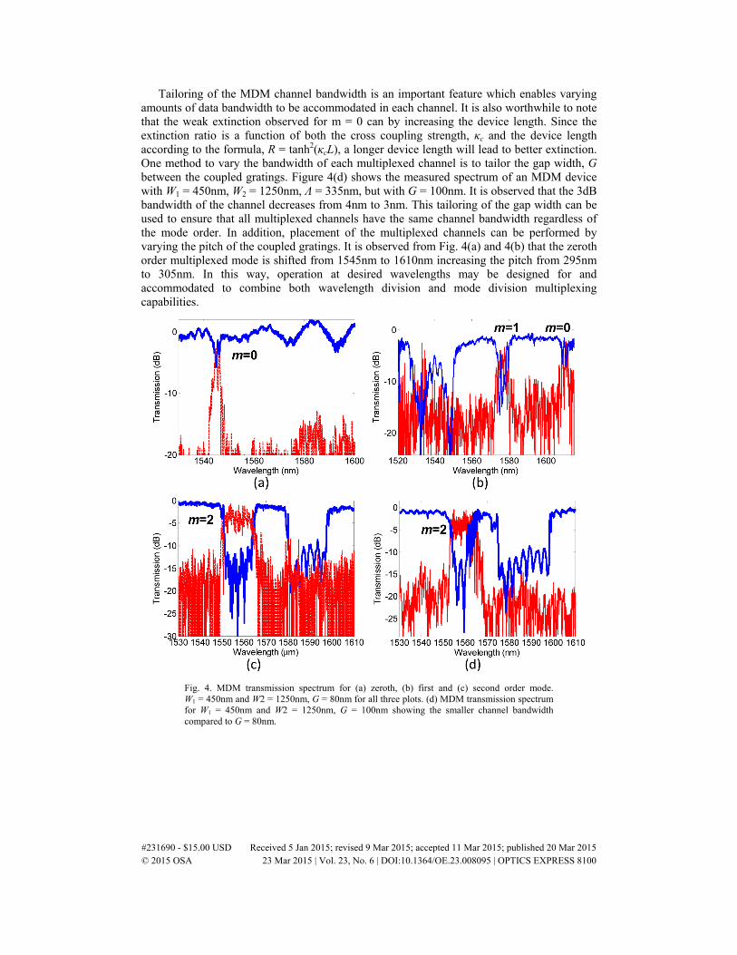
Figure 2 (a) shows the effective index as a function of waveguide width for the first five mode orders. It is observed that three mode orders exist for a waveguide with width W2 = 1250nm and five orders for W2 = 1850nm. For the MDM device to drop the selected mode at 1.55µm, the corrugation pitch needs to be adjusted according to Eq. (1). The sum of the propagation constants, β1 + β2 as a function of wavelength is plotted in Fig. 2(b). It is observed that within each waveguide width, β1 + β2 decreases as the mode order increases, thus implying that a larger value of Λ is needed to fulfill the MDM drop at 1.55µm. In addition, the modes for the first three mode orders for W2 = 1250nm and modes, m = 2, 3 and 4 for W2 = 1850 are calculated using a fully vectorial beam propagation method, and shown in Fig. 3(a)-3(f) respectively. Each of the right and left waveguides also possess a self – Bragg coupling effect, which results in a broad stop band located at self eff1,22. .nλ = Λ . Operationally,
the self – Bragg coupling effect from the right waveguide will show up within the C – band
#231690 - $15.00 USD Received 5 Jan 2015; revised 9 Mar 2015; accepted 11 Mar 2015; published 20 Mar 2015 © 2015 OSA 23 Mar 2015 | Vol. 23, No. 6 | DOI:10.1364/OE.23.008095 | OPTICS EXPRESS 8098
for some of the MDM devices below and therefore, should be considered when designing the devices.
3. Fabrication and characterization
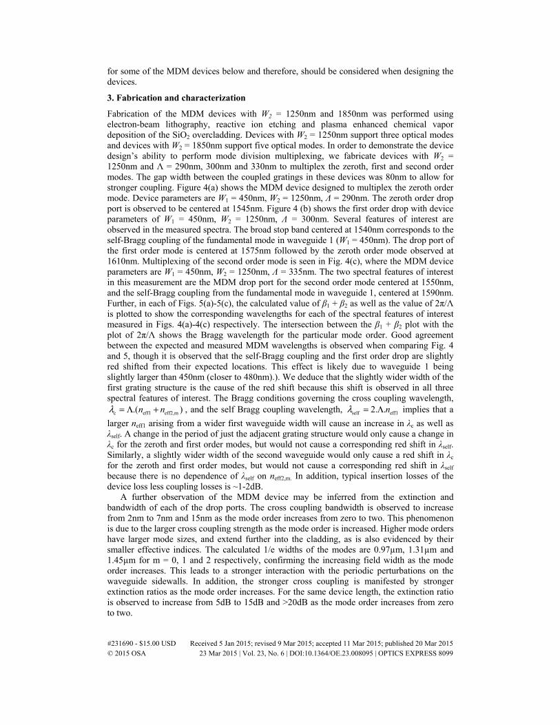
Fabrication of the MDM devices with W2 = 1250nm and 1850nm was performed using electron-beam lithography, reactive ion etching and plasma enhanced chemical vapor deposition of the SiO2 overcladding. Devices with W2 = 1250nm support three optical modes and devices with W2 = 1850nm support five optical modes. In order to demonstrate the device design’s ability to perform mode division multiplexing, we fabricate devices with W2 = 1250nm and Λ = 290nm, 300nm and 330nm to multiplex the zeroth, first and second order modes. The gap width between the coupled gratings in these devices was 80nm to allow for stronger coupling. Figure 4(a) shows the MDM device designed to multiplex the zeroth order mode. Device parameters are W1 = 450nm, W2 = 1250nm, Λ = 290nm. The zeroth order drop port is observed to be centered at 1545nm. Figure 4 (b) shows the first order drop with device parameters of W1 = 450nm, W2 = 1250nm, Λ = 300nm. Several features of interest are observed in the measured spectra. The broad stop band centered at 1540nm corresponds to the self-Bragg coupling of the fundamental mode in waveguide 1 (W1 = 450nm). The drop port of the first order mode is centered at 1575nm followed by the zeroth order mode observed at 1610nm. Multiplexing of the second order mode is seen in Fig. 4(c), where the MDM device parameters are W1 = 450nm, W2 = 1250nm, Λ = 335nm. The two spectral features of interest in this measurement are the MDM drop port for the second order mode centered at 1550nm, and the self-Bragg coupling from the fundamental mode in waveguide 1, centered at 1590nm. Further, in each of Figs. 5(a)-5(c), the calculated value of β1 + β2 as well as the value of 2π/Λ is plotted to show the corresponding wavelengths for each of the spectral features of interest measured in Figs. 4(a)-4(c) respectively. The intersection between the β1 + β2 plot with the plot of 2π/Λ shows the Bragg wavelength for the particular mode order. Good agreement between the expected and measured MDM wavelengths is observed when comparing Fig. 4 and 5, though it is observed that the self-Bragg coupling and the first order drop are slightly red shifted from their expected locations. This effect is likely due to waveguide 1 being slightly larger than 450nm (closer to 480nm).). We deduce that the slightly wider width of the first grating structure is the cause of the red shift because this shift is observed in all three spectral features of interest. The Bragg conditions governing the cross coupling wavelength,
c eff1 eff2,m.( )n nλ = Λ + , and the self Bragg coupling wavelength, self eff12. .nλ = Λ implies that a
larger neff1 arising from a wider first waveguide width will cause an increase in λc as well as λself. A change in the period of just the adjacent grating structure would only cause a change in λc for the zeroth and first order modes, but would not cause a corresponding red shift in λself. Similarly, a slightly wider width of the second waveguide would only cause a red shift in λc for the zeroth and first order modes, but would not cause a corresponding red shift in λself because there is no dependence of λself on neff2,m. In addition, typical insertion losses of the device loss less coupling losses is ~1-2dB.
A further observation of the MDM device may be inferred from the extinction and bandwidth of each of the drop ports. The cross coupling bandwidth is observed to increase from 2nm to 7nm and 15nm as the mode order increases from zero to two. This phenomenon is due to the larger cross coupling strength as the mode order is increased. Higher mode orders have larger mode sizes, and extend further into the cladding, as is also evidenced by their smaller effective indices. The calculated 1/e widths of the modes are 0.97µm, 1.31µm and 1.45µm for m = 0, 1 and 2 respectively, confirming the increasing field width as the mode order increases. This leads to a stronger interaction with the periodic perturbations on the waveguide sidewalls. In addition, the stronger cross coupling is manifested by stronger extinction ratios as the mode order increases. For the same device length, the extinction ratio is observed to increase from 5dB to 15dB and >20dB as the mode order increases from zero to two.
#231690 - $15.00 USD Received 5 Jan 2015; revised 9 Mar 2015; accepted 11 Mar 2015; published 20 Mar 2015 © 2015 OSA 23 Mar 2015 | Vol. 23, No. 6 | DOI:10.1364/OE.23.008095 | OPTICS EXPRESS 8099
Tailoring of the MDM channel bandwidth is an important feature which enables varying amounts of data bandwidth to be accommodated in each channel. It is also worthwhile to note that the weak extinction observed for m = 0 can by increasing the device length. Since the extinction ratio is a function of both the cross coupling strength, κc and the device length according to the formula, R = tanh2(κcL), a longer device length will lead to better extinction. One method to vary the bandwidth of each multiplexed channel is to tailor the gap width, G between the coupled gratings. Figure 4(d) shows the measured spectrum of an MDM device with W1 = 450nm, W2 = 1250nm, Λ = 335nm, but with G = 100nm. It is observed that the 3dB bandwidth of the channel decreases from 4nm to 3nm. This tailoring of the gap width can be used to ensure that all multiplexed channels have the same channel bandwidth regardless of the mode order. In addition, placement of the multiplexed channels can be performed by varying the pitch of the coupled gratings. It is observed from Fig. 4(a) and 4(b) that the zeroth order multiplexed mode is shifted from 1545nm to 1610nm increasing the pitch from 295nm to 305nm. In this way, operation at desired wavelengths may be designed for and accommodated to combine both wavelength division and mode division multiplexing capabilities.
Fig. 4. MDM transmission spectrum for (a) zeroth, (b) first and (c) second order mode. W1 = 450nm and W2 = 1250nm, G = 80nm for all three plots. (d) MDM transmission spectrum for W1 = 450nm and W2 = 1250nm, G = 100nm showing the smaller channel bandwidth compared to G = 80nm.
#231690 - $15.00 USD Received 5 Jan 2015; revised 9 Mar 2015; accepted 11 Mar 2015; published 20 Mar 2015 © 2015 OSA 23 Mar 2015 | Vol. 23, No. 6 | DOI:10.1364/OE.23.008095 | OPTICS EXPRESS 8100
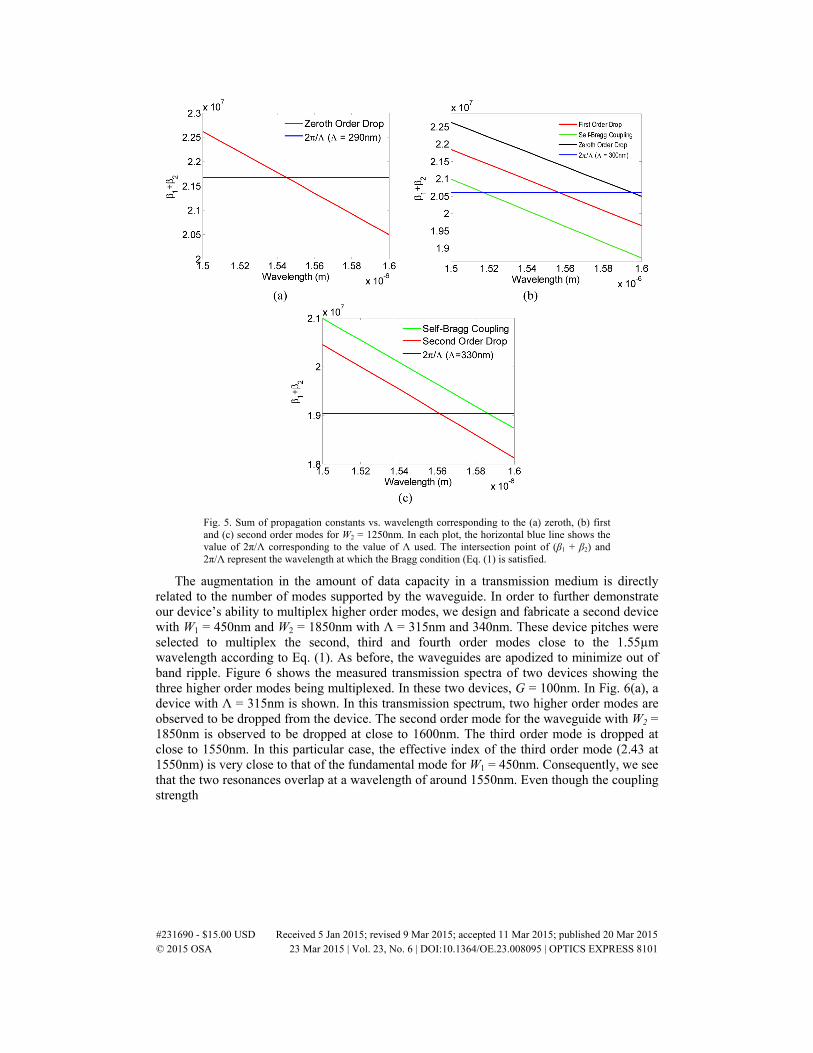
Fig. 5. Sum of propagation constants vs. wavelength corresponding to the (a) zeroth, (b) first and (c) second order modes for W2 = 1250nm. In each plot, the horizontal blue line shows the value of 2π/Λ corresponding to the value of Λ used. The intersection point of (β1 + β2) and 2π/Λ represent the wavelength at which the Bragg condition (Eq. (1) is satisfied.
The augmentation in the amount of data capacity in a transmission medium is directly related to the number of modes supported by the waveguide. In order to further demonstrate our device’s ability to multiplex higher order modes, we design and fabricate a second device with W1 = 450nm and W2 = 1850nm with Λ = 315nm and 340nm. These device pitches were selected to multiplex the second, third and fourth order modes close to the 1.55µm wavelength according to Eq. (1). As before, the waveguides are apodized to minimize out of band ripple. Figure 6 shows the measured transmission spectra of two devices showing the three higher order modes being multiplexed. In these two devices, G = 100nm. In Fig. 6(a), a device with Λ = 315nm is shown. In this transmission spectrum, two higher order modes are observed to be dropped from the device. The second order mode for the waveguide with W2 = 1850nm is observed to be dropped at close to 1600nm. The third order mode is dropped at close to 1550nm. In this particular case, the effective index of the third order mode (2.43 at 1550nm) is very close to that of the fundamental mode for W1 = 450nm. Consequently, we see that the two resonances overlap at a wavelength of around 1550nm. Even though the coupling strength
#231690 - $15.00 USD Received 5 Jan 2015; revised 9 Mar 2015; accepted 11 Mar 2015; published 20 Mar 2015 © 2015 OSA 23 Mar 2015 | Vol. 23, No. 6 | DOI:10.1364/OE.23.008095 | OPTICS EXPRESS 8101
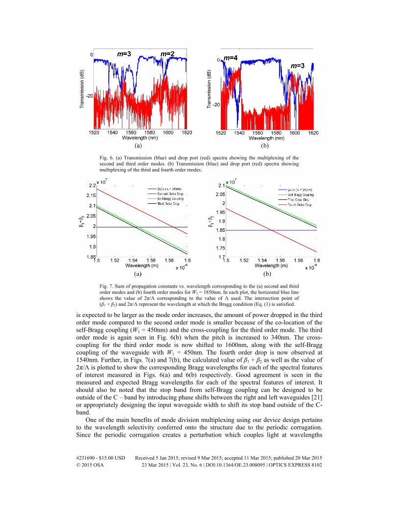
Fig. 6. (a) Transmission (blue) and drop port (red) spectra showing the multiplexing of the second and third order modes. (b) Transmission (blue) and drop port (red) spectra showing multiplexing of the third and fourth order modes.
Fig. 7. Sum of propagation constants vs. wavelength corresponding to the (a) second and third order modes and (b) fourth order modes for W2 = 1850nm. In each plot, the horizontal blue line shows the value of 2π/Λ corresponding to the value of Λ used. The intersection point of (β1 + β2) and 2π/Λ represent the wavelength at which the Bragg condition (Eq. (1) is satisfied.
is expected to be larger as the mode order increases, the amount of power dropped in the third order mode compared to the second order mode is smaller because of the co-location of the self-Bragg coupling (W1 = 450nm) and the cross-coupling for the third order mode. The third order mode is again seen in Fig. 6(b) when the pitch is increased to 340nm. The cross-coupling for the third order mode is now shifted to 1600nm, along with the self-Bragg coupling of the waveguide with W1 = 450nm. The fourth order drop is now observed at 1540nm. Further, in Figs. 7(a) and 7(b), the calculated value of β1 + β2 as well as the value of 2π/Λ is plotted to show the corresponding Bragg wavelengths for each of the spectral features of interest measured in Figs. 6(a) and 6(b) respectively. Good agreement is seen in the measured and expected Bragg wavelengths for each of the spectral features of interest. It should also be noted that the stop band from self-Bragg coupling can be designed to be outside of the C – band by introducing phase shifts between the right and left waveguides [21] or appropriately designing the input waveguide width to shift its stop band outside of the C-band.
One of the main benefits of mode division multiplexing using our device design pertains to the wavelength selectivity conferred onto the structure due to the periodic corrugation. Since the periodic corrugation creates a perturbation which couples light at wavelengths
#231690 - $15.00 USD Received 5 Jan 2015; revised 9 Mar 2015; accepted 11 Mar 2015; published 20 Mar 2015 © 2015 OSA 23 Mar 2015 | Vol. 23, No. 6 | DOI:10.1364/OE.23.008095 | OPTICS EXPRESS 8102

satisfying the Bragg condition in the counter-propagating direction, multiplexing using different mode orders can be combined with wavelength division multiplexing as well. This allows us to potentially have a device which combines both wavelength division multiplexing and mode division multiplexing to generate even greater data capacity on a chip.
4. Conclusions
We have demonstrated mode division multiplexers utilizing coupled waveguides possessing periodic corrugations on a silicon chip. MDM devices multiplexing the zeroth to second order modes and the second to fourth order modes are fabricated and experimentally characterized. Higher order modes are observed to have stronger extinction ratios and larger drop port bandwidths, implying a stronger coupling coefficient. Tailoring of the drop port bandwidth is also demonstrated by changing the gap width of the coupled device. This design feature enables us to ensure that multiplexed modes have the same drop port bandwidth regardless of mode order. Since the location of the drop port may also be tailored using the pitch of the device corrugation, strategies combining both wavelength (up to 100 channels within the C – band [4]) and mode division multiplexing (3 – 5 modes) may be employed to achieve transmission capacities two orders of magnitude greater than that available to a single transmission medium. Operation by way of counter-propagating modes in periodic structures enables this device to combine its mode division multiplexing capabilities with wavelength division multiplexing functionalities to further augment the multiplexing capacity of the device.
Acknowledgments
Support from the MOE ACRF Tier 2 Research Grant, A*STAR Public Sector Funding, SUTD-MIT International Design center and SUTD-ZJU Collaborative Research Grant is gratefully acknowledged.
#231690 - $15.00 USD Received 5 Jan 2015; revised 9 Mar 2015; accepted 11 Mar 2015; published 20 Mar 2015 © 2015 OSA 23 Mar 2015 | Vol. 23, No. 6 | DOI:10.1364/OE.23.008095 | OPTICS EXPRESS 8103