w83877atf winbond i/o - ic72. · pdf file3.0 uart port ... • report acpi status interrupt...
TRANSCRIPT

W83877ATF
WINBOND I/O

W83877ATF Data Sheet Revision History
Pages Dates VersionVersionon Web
Main Contents
1 n.a. 07/29/97 0.50 First published.
21,3,6,49,50,98,140,141,142,170 04/10/98 0.51 A1 Typo correction and data calibrated
3
4
5
6
7
8
9
10
Please note that all data and specifications are subject to change without notice. Allthe trade marks of products and companies mentioned in this data sheet belong totheir respective owners.
LIFE SUPPORT APPLICATIONSThese products are not designed for use in life support appliances, devices, orsystems where malfunction of these products can reasonably be expected to resultin personal injury. Winbond customers using or selling these products for use insuch applications do so at their own risk and agree to fully indemnify Winbond forany damages resulting from such improper use or sales.

W83877ATF
Publication Release Date: July 1997- I - Version 0.50
TABLE OF CONTENTS
GENERAL DESCRIPTION ................................................................................................1
FEATURES ..........................................................................................................................2
1.0 PIN CONFIGURATION ...............................................................................................4
1.0 PIN DESCRIPTION ........................................................................................................................5
1.1 HOST INTERFACE .........................................................................................................................5
1.2 SERIAL PORT INTERFACE ...........................................................................................................7
1.3 MULTI-MODE PARALLEL PORT..................................................................................................9
1.4 FDC INTERFACE..........................................................................................................................14
2.0 FDC FUNCTIONAL DESCRIPTION........................................................................16
2.1 W83877ATF FDC...........................................................................................................................16
2.2 REGISTER DESCRIPTIONS .........................................................................................................28
3.0 UART PORT................................................................................................................39
3.1 UNIVERSAL ASYNCHRONOUS RECEIVER/TRANSMITTER (UART A, UART B)..................39
3.2 REGISTER ADDRESS...................................................................................................................40
3.3 INFRARED PORT .........................................................................................................................49
4.0 PARALLEL PORT.....................................................................................................82
4.1 PRINTER INTERFACE LOGIC.....................................................................................................82
4.2 ENHANCED PARALLEL PORT (EPP) .........................................................................................84
4.3 EXTENDED CAPABILITIES PARALLEL (ECP) PORT...............................................................88
4.4 EXTENSION FDD MODE (EXTFDD)...........................................................................................97
4.5 EXTENSION 2FDD MODE (EXT2FDD).......................................................................................97
5.0 PLUG AND PLAY CONFIGURATION ....................................................................98
6.0 ACPI /LEGACY FEATURE AND AUTO POWER MANAGEMENT .....................98
6.1 ACPI/LEGACY POWER MANAGEMENT ...................................................................................98
6.2 DEVICE(AUTO) POWER MANAGEMENT..................................................................................98
7.0 SERIAL IRQ.................................................................................................................99

W83877ATF
Publication Release Date: July 1997- II - Version 0.50
7.1 START FRAME ...........................................................................................................................100
7.2 IRQ/DATA FRAME .....................................................................................................................100
7.3 STOP FRAME..............................................................................................................................101
7.4 RESET AND INITIALIZATION ..................................................................................................101
8.0 EXTENDED FUNCTION REGISTERS ..................................................................102
8.1 EXTENDED FUNCTIONS ENABLE REGISTERS (EFERS)...........................................................102
8.2 EXTENDED FUNCTION INDEX REGISTERS (EFIRS), EXTENDED FUNCTION DATAREGISTERS (EFDRS) ...................................................................................................................103
8.3 ACPI REGISTERS FEATURES .......................................................................................................150
8.4 ACPI REGISTERS (ACPIRS)...........................................................................................................152
9.0 SPECIFICATIONS....................................................................................................166
9.1 ABSOLUTE MAXIMUM RATINGS............................................................................................166
9.2 DC CHARACTERISTICS ............................................................................................................166
9.3 AC CHARACTERISTICS ............................................................................................................168
10.0 TIMING WAVEFORMS ........................................................................................174
10.1 FDC..............................................................................................................................................174
10.2 UART/PARALLEL.......................................................................................................................175
10.3 PARALLEL PORT .......................................................................................................................177
11.0 APPLICATION CIRCUITS....................................................................................183
11.1 PARALLEL PORT EXTENSION FDD ........................................................................................183
11.2 PARALLEL PORT EXTENSION 2FDD.......................................................................................184
11.3 FOUR FDD MODE......................................................................................................................184
12.0 ORDERING INFORMATION ...............................................................................185
13.0 HOW OT READ THE TOP MARKING ...............................................................185
14.0 PACKAGE DIMENSIONS .....................................................................................186

W83877ATF
WINBOND I/O
Publication Release Date: April 1998- 1 - Version 0.51
GENERAL DESCRIPTIONThe W83877ATF is an enhanced version from Winbond's most popular I/O chip W83877F --- whichintegrates the disk drive adapter, serial port (UART), IrDA 1.0 SIR, parallel port, configurable plug-and-play registers for the whole chip --- plus additional powerful features: IrDA 1.1 (MIR for 1.152Mbps or FIR for 4M bps), TV remote IR, ACPI, serial IRQ, full 16-bit address decoding, and ACPIcompliant.
The disk drive adapter functions of W83877ATF include a floppy disk drive controller compatible withthe industry standard 82077/765, data separator, write pre-compensation circuit, decode logic, datarate selection, clock generator, drive interface control logic, and interrupt and DMA logic. The widerange of functions integrated onto the W83877ATF greatly reduces the number of componentsrequired for interfacing with floppy disk drives. The W83877ATF supports four 360K, 720K, 1.2M,1.44M, or 2.88M disk drives and data transfer rates of 250 Kb/S, 300 Kb/S, 500 Kb/S,1 Mb/S, and 2Mb/S.
The W83877ATF provides two high-speed serial communication ports (UARTs), one of whichsupports serial Infrared communication. Each UART includes a 16-byte send/receive FIFO, aprogrammable baud rate generator, complete modem control capability, and a processor interruptsystem. One of the UARTs supporting infrared (IR) includes 32-byte FIFO, serial IR, 1.152M bps MIR,0.576M bps, 4M bps FIR, and TV remote IR (supporting NEC, RC-5, extended RC-5, and RECS-80protocols). Both UARTs provide legacy speed with baud rate 115.2k, and provide advanced speedwith baud rate 230k, 460k, and 921k bps which support higher speed Modems.
The W83877ATF supports one PC-compatible printer port (SPP), Bi-directional Printer port (BPP)and also Enhanced Parallel Port (EPP) and Extended Capabilities Port (ECP). Through the printerport interface pins, also available are: Extension FDD Mode and Extension 2FDD Mode allowing oneor two external floppy disk drives to be connected to the notebook computer.
Winbond W83877ATF provides functions that comply with ACPI (Advanced Configuration and Power
Interface), which includes support of legacy and ACPI power management through SMI or SCIfunction pins. One 24-bit power management timer is implemented with carry notify interrupt.W83877ATF also has auto power management to reduce power consumption.
The Serial IRQ for PCI architecture is supported, ISA IRQs (IRQ1~IRQ15) can be cascaded into oneIRQ pin. W83877ATF also features ISA bus IRQ sharing and allows two or more devices to share thesame IRQ.
W83877ATF is made to fully comply with MicrosoftTM PC97 Hardware Design Guide. IRQs, DMAs,and I/O space resource are flexible to adjust to meet ISA PnP requirements. Moreover, W83877ATFis made to meet the specification of PC97's requirement in the power management: ACPI and DPM(Device Power Management).
The configuration registers support mode selection, function enable/disable, and power down functionselection. Furthermore, the configurable PnP features are compatible with the plug-and-play featuredemand of Windows 95TM, which makes system resource allocation more efficient than ever.
Another benifit is that W83877ATF has the same pin assignment as W83877F, W83877AF,W83877TF. Thius makes the design very flexible.

W83877ATF
Publication Release Date: April 1998- 2 - Version 0.51
FEATURES
General:
• Plug & Play 1.0A Compliant
• Support 8 IRQs (ISA), or 15 IRQs (Serial IRQ), 4 DMA channels, and 480 Relocatable addresses
• Capable of ISA Bus IRQ Sharing
• Compliant with Microsoft TM PC97 Hardware Design Guide
• Support DPM (Device Power Management), ACPI
• Report ACPI status interrupt by nSCI signal from serial IRQ pin, or from IRQ A~H pins
• Single 24M or 48M Hz crystal input
FDC:
• Compatible with IBMTM PC AT disk drive systems
• Variable write pre-compensation with track selectable capability
• DMA enable logic
• Support floppy disk drives and tape drives
• Detects all overrun and underrun conditions
• Built-in address mark detection circuit to simplify the read electronics
• FDD anti-virus functions with software write protect and FDD write enable signal (write data signalis forced to be inactive)
• Support up to four 3.5-inch or 5.25-inch floppy disk drives
• Completely compatible with industry standard 82077
• 360K/720K/1.2M/1.44M/2.88M format; 250K, 300K, 500K, 1M, 2M bps data transfer rate
• Support vertical recording format
• Support 3-mode FDD, and its Windows95TM driver
• 16-byte data FIFOs
UART:
• Two high-speed 16550 compatible UARTs with 16-byte send/receive FIFOs
• MIDI compatible
• Fully programmable serial-interface characteristics:
− 5, 6, 7 or 8-bit characters
− Even, odd or no parity bit generation/detection
− 1, 1.5 or 2 stop bits generation

W83877ATF
Publication Release Date: April 1998- 3 - Version 0.51
• Internal diagnostic capabilities:
− Loop-back controls for communications link fault isolation
− Break, parity, overrun, framing error simulation
• Programmable baud generator allows division of 1.8461 M Hz and 24 MHz by 1 to (216-1)
• Maximum baud rate up to 921k bps for 14.768M Hz and 1.5M bps for 24M Hz
Infrared:
• Support IrDA version 1.0 SIR protocol with maximum baud rate up to 115.2K bps
• Support SHARP ASK-IR protocol with maximum baud rate up to 57,600 bps
• Support IrDA version 1.1 MIR (1.152M bps) and FIR (4M bps) protocol
− Single DMA channel for transmitter or receiver
− 32-byte FIFO is supported in both FIR TX/RX transmission
− 8-byte status FIFO is supported to store received frame status (such as overrun, CRC error, etc.)
• Support auto-config SIR and FIR
• Support full Customer IR
• Support driver for MicrosoftTM Windows 95TM and Windows 98TM (Memphis TM)
Parallel Port:
• Compatible with IBM TM parallel port
• Support PS/2 compatible bi-directional parallel port
• Support Enhanced Parallel Port (EPP) − Compatible with IEEE 1284 specification
• Support Extended Capabilities Port (ECP) − Compatible with IEEE 1284 specification
• Extension FDD mode supports disk drive B and Extension 2FDD mode supports disk drives A and Bthrough parallel port
• Enhanced printer port back-drive current protection
Others:
• Programmable configuration settings
• Immediate or automatic power-down mode for power management
• All hardware power-on settings have internal pull-up or pull-down resistors as default value
• Full 16-bit address decode (UART B pin option)
• PNF pin (Printer-Not-Floppy pin) for distinguishing printer port connection --- FDD or Printer; uniquefor notebook application of external floppy through printer port
Package:
• 100-pin QFP (W83877ATF), and also 100-pin TQFP (W83877ATD)
W83877ATF
Publication Release Date: April 1998- 4 - Version 0.51
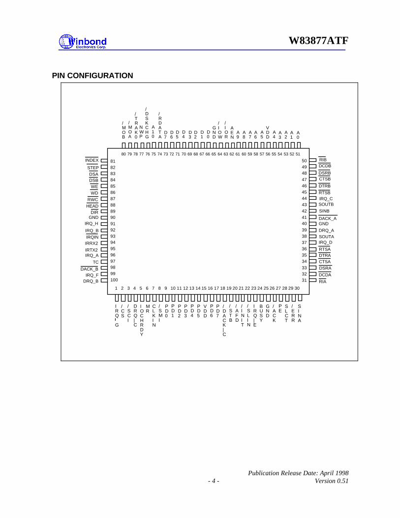
PIN CONFIGURATION
/MOB
/MOA
/TRAK0
NWP
/DSKCHG
A10
/RDATA
D7
D6
D5
D4
D3
D2
D1
D0
GND
/IOW
/IOR
AEN
A9
A8
A7
A6
A5
VDD
A4
A3
A2
A1
A0
X X X X X X X X XXX X X X XX X X X X X X X X X X X X XX
X
X
X
X
X
X
X
X
X
X
X
X
X
X
X
X
X
X
X
X
X
X
X
X
X
X
X
X
X
X
X
X
X
X
X
X
X
X
X
X
X X X X X X X XX X X X XX X X X X X X X
81828384858687888990919293949596979899100
504948
474645444342
4140
393837363534
333231
80 79 78 77 76 75 74 73 72 71 70 69 68 67 66 65 64 63 62 61 60 59 58 57 56 55 54 53 52 51
1 2 3 4 5 6 7 8 9 10 11 12 13 14 15 16 17 18 19 20 21 22 23 24 25 26 27 28 29 30
RIBDCDB
DSRBCTSB
DTRB
RTSBIRQ_CSOUTB
SINB
DACK_AGND
DRQ_ASOUTAIRQ_D
RTSADTRACTSA
DSRA
DCDA
RIA
IRQ
G
/CS
/SCI
DRQ|C
IOCHRDY
MR
CLKIN
/SMI
PD0
PD1
PD2
PD3
PD4
VDD
PD5
PD6
PD7
/DACK|C
/STB
/AFD
/INIT
/SLIN
IRQ|E
BUSY
GND
/ACK
PE
SLCT
/ERR
SINA
INDEX
STEP
DSADSBWE
WD
RWC
HEADDIR
GNDIRQ_H
IRQ_B
IRQINIRRX2
IRTX2IRQ_A
TC
DACK_BIRQ_F
DRQ_B

W83877ATF
Publication Release Date: April 1998- 5 - Version 0.51
1.0 PIN DESCRIPTIONNote: Refer to section 9.2 DC CHARACTERISTICS for details.
I/O8tc - TTL level output pin with 8 mA source-sink capability; CMOS level input voltage
I/O12t - TTL level bi-directional pin with 12 mA source-sink capability
I/O12ts - TTL level bi-directional pin with 12 mA source-sink capability and Schmitt-triggered input
I/O24t - TTL level bi-directional pin with 24 mA source-sink capability
OUT8t - TTL level output pin with 8 mA source-sink capability
OUT12t - TTL level output pin with 12 mA source-sink capability
OD12 - Open-drain output pin with 12 mA sink capability
OD24 - Open-drain output pin with 24 mA sink capability
INt - TTL level input pin
INts - TTL level Schmitt-triggered input pin
INcs - CMOS level Schmitt-triggered input pin
1.1 HOST INTERFACE
SYMBOL PIN I/O FUNCTION
D0−D7 66-73 I/O24t System data bus bits 0-7.
A0−A10 51-55
57-61
75
INt System address bus bits 0-10.
IOCHRDY 5 OD24 In EPP Mode, this pin is the I/O Channel Ready output to extendthe host read/write cycle.
MR 6 INts Master Reset. Active high. MR is low during normal operations.
CS 2 INts Active low chip select signal.
A11 INts System address bus bit 11, when 16-bit address decoder is set tologic 0 in which CR16.bit6 (EN SA16 ).
AEN 62 INt System address bus enable.
IOR 63 INts CPU I/O read signal.
IOW 64 INts CPU I/O write signal.
DACK_ A 41 INts DMA acknowledge signal A.
DRQ_A 39 OUT8t DMA request signal A.
DRQ_B 100 OUT12t DMA request signal B.
DACK_B 98 INts DMA acknowledge signal B.

W83877ATF
Publication Release Date: April 1998- 6 - Version 0.51
1.1 Host Interface, continued
SYMBOL PIN I/O FUNCTION
DRQ_C 4 OUT12t DMA request signal C.
DACK_C 18 INts DMA acknowledge signal C.
IRQIN 93 INts Interrupt request input.
DRQ_D OUT12t DMA request signal D.
IRSL2 OUT12t IR module mode selection 2.
IRRXH/IRSL0 I/O12ts When input, acts as a function of high speed IR receivingterminal. When output selected, acts as a IR module modeselection 0.
PNF INts Detects printer is active, and not external FDC. When this pinPNF is detected to 1 signal, the device is switched to parallelprinter. When this pin PNF is detected to 0 signal, the device isswitched to external FDC. The pin is configured in CR16.bit7(ENPNF).
IRRXH/IRSL0 3 I/O12ts When input pin, high speed IR received terminal. When outputpin, IR module mode select 0. Input or output are definied inhigh speed IR register.
DACK_D INts DMA acknowledge signal for channel D.
IRSL1 OUT12t IR module mode select 1.
TC 97 INts Terminal Count. When active, this pin indicates termination ofa DMA transfer.
IRQ_ A 96 OUT12t When CR16 Bit 5 (GOIQSEL) = 0: Interrupt request signal A.
SCI OUT12t ACPI interrupt signal, selected by PnP IRQ configure register.
GIO1 I/O12t When CR16 Bit 4 (GOIQSEL) = 1: General Purpose I/O port 1.
IRQ_B 92 OUT12t When CR16 Bit 4 (GOIQSEL) = 0: Interrupt request signal B.
GIO0 I/O12t When CR16 Bit 4 (GOIQSEL) = 1: General Purpose I/O port 0.
IRQ_C 44 OUT12t Interrupt request signal C.
IRQ_D 37 OUT12t Interrupt request signal D.
IRQ_E 23 OUT12t Interrupt request signal E.
IRQ_F 99 OUT12t Interrupt request signal F.
IRQ_G 1 OUT12t Interrupt request signal G.
DRQ_D OUT12t DMA request signal channel D.
IRSL2 OUT12t IR module mode select 2.
PCICLK INt PCI clock input when the serial IRQ function is selected.

W83877ATF
Publication Release Date: April 1998- 7 - Version 0.51
1.1 Host Interface, continued
SYMBOL PIN I/O FUNCTION
IRQ_H 91 OUT12t Interrupt request signal H.
IRSL2 OUT12t IR module mode selection 2.
DACK_D INts DMA acknowledge signal D.
SERIRQ OUT12t Serial Interrupt output, when the function of the serial IRQ is setto logic 1 defined in the CR31.bit2 (IRQMODS).
CLKIN 7 INt 24MHz/48MHZ clock input. CLKINSEL bit in CR2C registershould be correctly reset/set according to the input frequency.
SMI 8 OUT12t For the power management, the SMI is and active low by thepower management events, that generate an nSCI in ACPImode.
1.2 Serial Port Interface
SYMBOL PIN I/O FUNCTION
CTSA 34 INt Clear To Send is the modem control input.
CTSB 47 INt Clear To Send is the modem control input.
A12 INt System address bus bit 12, when 16-bit address decoder isselected, that is, nEN16SA (CR16.bit6) is set to logic 0.
DSRA 33 INt Data Set Ready. An active low indicates the modem or data setis ready to establish a communication link and transfer data tothe UART.
DSRB 48 INt Data Set Ready. An active low indicates the modem or data setis ready to establish a communication link and transfer data tothe UART.
A13 INt System address bus bit 13, when 16-bit address decoder isselected.
DCDA 32 INt Data Carrier Detect. An active low indicates the modem or dataset has detected a data carrier.
DCDB 49 INt Data Carrier Detect. An active low indicates the modem or dataset has detected a data carrier.
A14 INt System address bus bit 14, when 16-bit address decoder isselected.
RIA 31 INt Ring Indicator. An active low indicates that a ring signal is beingreceived by the modem or data set.

W83877ATF
Publication Release Date: April 1998- 8 - Version 0.51
1.2 Serial Port Interface, continued
SYMBOL PIN I/O FUNCTION
RIB 50 INt Ring Indicator. An active low indicates that a ring signal is beingreceived by the modem or data set.
A15 INt System address bus bit 15, when 16-bit address decoder isselected.
SINA 30 INt Serial Input of COM A. Used to receive serial data from thecommunication link.
SINB 42 INt Serial Input of COM B. Used to receive serial data from thecommunication link.
IRRX1 INt When infrared function is selected, acts as infrared input.
SOUTA 38 I/O8tc UART A Serial Output. Used to transmit serial data out to thecommunication link.
PEN16SA INt During power-on reset, this pin is pulled up internally and isdefined as PEN16SA, which provides the power-on value forCR2E.bit6 (PEN16SA ). A 4.7 kΩ is recommended whenintending to pull down at power-on reset.
SOUTB 43 I/O12t UART B Serial Output. Used to transmit serial data out to thecommunication link.
IRTX1 INt Infrared serial data output when COM B acts as infrared port.
DTRA 35 I/O8tc UART A Data Terminal Ready. An active low informs themodem or data set that the controller is ready to communicate.
PHEFRAS INt During power-on reset, this pin is pulled down internally and isdefined as PHEFRAS, which provides the power-on value forCR16 bit 0 (HEFRAS), and Configuration Port is defined at 250h.A 4.7 kΩ is recommended when intending to pull up at power-onreset, and Configuration Port is defined at 3F0h.
DTRB 46 I/O8t UART B Data Terminal Ready. An active low informs themodem or data set that controller is ready to communicate.
RTSA 36 I/O8tc UART A Request To Send. An active low informs the modem ordata set that the controller is ready to send data.
PPNPCVS INt During power-on reset, this pin is pulled up internally and isdefined as PPNPCVS, which provides the power-on value forCR16 bit 2 (PNPCVS). A 4.7 kΩ is recommended whenintending to pull down at power-on reset.

W83877ATF
Publication Release Date: April 1998- 9 - Version 0.51
1.2 Serial Port Interface, continued
SYMBOL PIN I/O FUNCTION
RTSB 45 I/O8tc UART B Request To Send. An active low informs the modem ordata set that the controller is ready to send data.
PGOIQSEL INt During power-on reset, this pin is pulled down internally and isdefined as PGOIQSEL, which provides the power-on value forCR16 bit 4 (GOIQSEL). A 4.7 kΩ is recommended whenintending to pull up at power-on reset.
IRTX2 95 OUT12t Function as a InfraRed transmission data line.
IRRX2 94 INt Function as a InfraRed receiving line.
1.3 Multi-Mode Parallel Port
The following pins have eight functions, which are controlled by bits PRTMOD0, PRTMOD1, andPRTMOD2 of CR0 and CR9 (refer to section 8.0, Extended Functions).
SYMBOL PIN I/O FUNCTION
BUSY 24 INt PRINTER MODE: BUSY
An active high input indicates that the printer is not ready toreceive data. This pin is pulled high internally. Refer to thedescription of the parallel port for the definition of this pin in ECPand EPP mode.
OD12 EXTENSION FDD MODE: MOB2
This pin is for Extension FDD B; the function of this pin is thesame as that of the MOB pin.
OD12 EXTENSION 2FDD MODE: MOB2
This pin is for Extension FDD A and B; the function of this pin isthe same as that of the MOB pin.
ACK 26 INt PRINTER MODE: ACK
An active low input on this pin indicates that the printer hasreceived data and is ready to accept more data. This pin ispulled high internally. Refer to the description of the parallel portfor the definition of this pin in ECP and EPP mode.
OD12 EXTENSION FDD MODE: DSB2
This pin is for the Extension FDD B; its functions are the sameas those of the DSB pin.
OD12 EXTENSION 2FDD MODE: DSB2
This pin is for Extension FDD A and B; the function of this pin isthe same as that of the DSB pin.

W83877ATF
Publication Release Date: April 1998- 10 - Version 0.51
1.3 Multi-Mode Parallel Port, continued
SYMBOL PIN I/O FUNCTION
PE 27 INt PRINTER MODE: PE
An active high input on this pin indicates that the printer hasdetected the end of the paper. This pin is pulled high internally.
Refer to the description of the parallel port for the definition ofthis pin in ECP and EPP mode.
OD12 EXTENSION FDD MODE: WD2
This pin is for Extension FDD B; its function is the same as thatof the WD pin.
OD12 EXTENSION 2FDD MODE: WD2
This pin is for Extension FDD A and B; the function of this pin isthe same as that of the WD pin.
JOYSTICK MODE: NC pin.
SLCT 28 INt PRINTER MODE: SLCT
An active high input on this pin indicates that the printer isselected. This pin is pulled high internally. Refer to thedescription of the parallel port for the definition of this pin in ECPand EPP mode.
OD12 EXTENSION FDD MODE: WE2
This pin is for Extension FDD B; its functions are the same asthose of the WE pin.
OD12 EXTENSION 2FDD MODE: WE2
This pin is for Extension FDD A and B; the function of this pin is
the same as that of the WE pin.
ERR 29 INt PRINTER MODE: ERR
An active low input on this pin indicates that the printer hasencountered an error condition. This pin is pulled high internally.Refer to the description of the parallel port for the definition ofthis pin in ECP and EPP mode.
OD12 EXTENSION FDD MODE: HEAD2
This pin is for Extension FDD B; its function is the same as thatof the HEADpin.
OD12 EXTENSION 2FDD MODE: HEAD2
This pin is for Extension FDD A and B; its function is the sameas that of the HEAD pin.

W83877ATF
Publication Release Date: April 1998- 11 - Version 0.51
1.3 Multi-Mode Parallel Port, continued
SYMBOL PIN I/O FUNCTION
SLIN 22 OD12 PRINTER MODE: SLIN
Output line for detection of printer selection. This pin is pulledhigh internally. Refer to the description of the parallel port for thedefinition of this pin in ECP and EPP mode.
OD12 EXTENSION FDD MODE: STEP2
This pin is for Extension FDD B; its function is the same as thatof the STEP pin.
OD12 EXTENSION 2FDD MODE: STEP2
This pin is for Extension FDD A and B; its function is the sameas that of the STEP pin .
INIT 21 OD12 PRINTER MODE: INIT
Output line for the printer initialization. This pin is pulled highinternally. Refer to the description of the parallel port for thedefinition of this pin in ECP and EPP mode.
OD12 EXTENSION FDD MODE: DIR2
This pin is for Extension FDD B; its function is the same as thatof the DIR pin.
OD12 EXTENSION 2FDD MODE: DIR2
This pin is for Extension FDD A and B; its function is the sameas that of the DIR pin.
AFD 20 OD12 PRINTER MODE: AFD
An active low output from this pin causes the printer to auto feeda line after a line is printed. This pin is pulled high internally.Refer to the description of the parallel port for the definition ofthis pin in ECP and EPP mode.
OD12 EXTENSION FDD MODE: RWC2
This pin is for Extension FDD B; its function is the same as thatof the RWC pin.
OD12 EXTENSION 2FDD MODE: RWC2
This pin is for Extension FDD A and B; its function is the sameas that of the RWC pin.

W83877ATF
Publication Release Date: April 1998- 12 - Version 0.51
1.3 Multi-Mode Parallel Port, continued
SYMBOL PIN I/O FUNCTION
STB 19 OD12 PRINTER MODE: STB
An active low output is used to latch the parallel data into theprinter. This pin is pulled high internally. Refer to the descriptionof the parallel port for the definition of this pin in ECP and EPPmode.
- EXTENSION FDD MODE: No Connection
This pin is a tri-state output.
- EXTENSION 2FDD MODE: No Connection
This pin is a tri-state output.
PD0 9 I/O24t PRINTER MODE: PD0
Parallel port data bus bit 0. Refer to the description of theparallel port for the definition of this pin in ECP and EPP mode.
INt EXTENSION FDD MODE: INDEX2
This pin is for Extension FDD B; the function of this pin is thesame as that of the INDEX pin. This pin is pulled high internally.
INt EXTENSION 2FDD MODE: INDEX2
This pin is for Extension FDD A and B; the function of this pin isthe same as INDEX pin. This pin is pulled high internally.
PD1 10 I/O24t PRINTER MODE: PD1
Parallel port data bus bit 1. Refer to the description of theparallel port for the definition of this pin in ECP and EPP mode.
INt EXTENSION FDD MODE: TRAK02
This pin is for Extension FDD B; the function of this pin is thesame as that of the TRAK0 pin. This pin is pulled high internally.
INt EXTENSION. 2FDD MODE: TRAK02
This pin is for Extension FDD A and B; the function of this pin isthe same as TRAK0 pin. This pin is pulled high internally.

W83877ATF
Publication Release Date: April 1998- 13 - Version 0.51
1.3 Multi-Mode Parallel Port, continued
SYMBOL PIN I/O FUNCTION
PD2 11 I/O24t PRINTER MODE: PD2
Parallel port data bus bit 2. Refer to the description of theparallel port for the definition of this pin in ECP and EPP mode.
INt EXTENSION FDD MODE: WP2
This pin is for Extension FDD B; the function of this pin is thesame as that of the WP pin. This pin is pulled high internally.
INt EXTENSION. 2FDD MODE: WP2
This pin is for Extension FDD A and B; the function of this pin isthe same as that of the WP pin. This pin is pulled highinternally.
PD3 12 I/O24t PRINTER MODE: PD3Parallel port data bus bit 3. Refer to the description of theparallel port for the definition of this pin in ECP and EPP mode.
INt EXTENSION FDD MODE: RDATA2Motor on B for Extension FDD B; the function of this pin is thesame as that of the RDATA pin. This pin is pulled high internally.
INt EXTENSION 2FDD MODE: RDATA2This pin is for Extension FDD A and B; the function of this pin isthe same as that of the RDATA pin. This pin is pulled highinternally.
PD4 13 I/O24t PRINTER MODE: PD4Parallel port data bus bit 4. Refer to the description of theparallel port for the definition of this pin in ECP and EPP mode.
INt EXTENSION FDD MODE: DSKCHG2Drive select B for Extension FDD B; the function of this pin is thesame as that of DSKCHG pin. This pin is pulled high internally.
INt EXTENSION 2FDD MODE: DSKCHG2This pin is for Extension FDD A and B; the function of this pin isthe same as that of the DSKCHG pin. This pin is pulled highinternally.
PD5 14 I/O24t PRINTER MODE: PD5Parallel port data bus bit 5. Refer to the description of theparallel port for the definition of this pin in ECP and EPP mode.
- EXTENSION FDD MODE: No ConnectionThis pin is a tri-state output.
- EXTENSION 2FDD MODE: No ConnectionThis pin is a tri-state output.

W83877ATF
Publication Release Date: April 1998- 14 - Version 0.51
1.3 Multi-Mode Parallel Port, continued
SYMBOL PIN I/O FUNCTION
PD6 16 I/O24t PRINTER MODE: PD6
Parallel port data bus bit 6. Refer to the description of theparallel port for the definition of this pin in ECP and EPP mode.
- EXTENSION FDD MODE:This pin is a tri-state output.
IOD24 EXTENSION. 2FDD MODE: MOA2
This pin is for Extension FDD A; its function is the same as thatof the MOA pin.
PD7 17 I/O24t PRINTER MODE: PD7
Parallel port data bus bit 7. Refer to the description of theparallel port for the definition of this pin in ECP and EPP mode.
- EXTENSION FDD MODE: This pin is a tri-state output.
OD24 EXTENSION 2FDD MODE: DSA2
This pin is for Extension FDD A; its function is the same as thatof the DSA pin.
1.4 FDC Interface
SYMBOL PIN I/O FUNCTION
RDATA 74 INcs The read data input signal from the FDD. This input pin is pulledup internally by an approximately 1K ohm resistor. The resistorcan be disabled by bit 4 of CR6 (FIPURDWN).
DSKCHG 76 INcs Diskette change. This signal is active low at power on andwhenever the diskette is removed. This input pin is pulled upinternally by an approximately 1K ohm resistor. The resistor canbe disabled by bit 4 of CR6 (FIPURDWN).
WP 77 INcs Write protected. This active low schmitt input from the disk driveindicates that the diskette is write-protected. This input pin ispulled up internally by an approximately 1K ohm resistor. Theresistor can be disabled by bit 4 of CR6 (FIPURDWN).
TRAK0 78 INcs Track 0. This schmitt input from the disk drive is active low whenthe head is positioned over the outermost track. This input pin ispulled up internally by an approximately 1K ohm resistor. Theresistor can be disabled by bit 4 of CR6 (FIPURDWN).

W83877ATF
Publication Release Date: April 1998- 15 - Version 0.51
1.4 FDC interface, continued
SYMBOL PIN I/O FUNCTION
INDEX 81 INcs This schmitt input from the disk drive is active low when the headis positioned over the beginning of a track marked by an indexhole. This input pin is pulled up internally by an approximately 1Kohm resistor. The resistor can be disabled by bit 4 of CR6(FIPURDWN).
MOA 79 OD24 Motor A On. When set to 0, this pin enables disk drive 0. This isan open drain output.
MOB 80 OD24 Motor B On. When set to 0, this pin enables disk drive 1. This isan open drain output.
STEP 82 OD24 Step output pulses. This active low open drain output produces apulse to move the head to another track.
DSA 83 OD24 Drive Select A. When set to 0, this pin enables disk drive A. Thisis an open drain output.
DSB 84 OD24 Drive Select B. When set to 0, this pin enables disk drive B. Thisis an open drain output.
WE 85 OD24 Write enable. An open drain output.
WD 86 OD24 Write data. This logic low open drain writes precompensationserial data to the selected FDD. An open drain output.
RWC 87 OD24 Reduced write current. This signal can be used on two-speed diskdrives to select the transfer rate. An open drain output.Logic 0 = 250 Kb/sLogic 1 = 500 Kb/sWhen bit 5 of CR9 (EN3MODE) is set to high, the three-modeFDD function is enabled, and the pin will have a differentdefinition. Refer to the EN3MODE bit in CR9.
HEAD 88 OD24 Head select. This open drain output determines which disk drivehead is active.Logic 1 = side 0Logic 0 = side 1
DIR 89 OD24 Direction of the head step motor. An open drain output.Logic 1 = outward motionLogic 0 = inward motion
VDD 15,56
+5 power supply for the digital circuitry
GND 25,4065,90
Ground

W83877ATF
Publication Release Date: April 1998- 16 - Version 0.51
2.0 FDC FUNCTIONAL DESCRIPTION
2.1 W83877ATF FDC
The floppy disk controller of the W83877ATF integrates all of the logic required for floppy diskcontrol. The FDC implements a PC/AT or PS/2 solution. All programmable options default tocompatible values. The FIFO provides better system performance in multi-master systems. Thedigital data separator supports up to data rate 1 M bits/sec or 2 M bits/sec.
The FDC includes the following blocks: AT interface, Precompensation, Data Rate Selection, DigitalData Separator, FIFO, and FDC Core.
2.1.1 AT interface
The interface consists of the standard asynchronous signals: RD , WR, A0-A3, IRQ, DMA control,and a data bus. The address lines select between the configuration registers, the FIFO andcontrol/status registers. This interface can be switched between PC/AT, Model 30, or PS/2 normalmodes. The PS/2 register sets are a superset of the registers found in a PC/AT.
2.1.2 FIFO (Data)
The FIFO is 16 bytes in size and has programmable threshold values. All command parameterinformation and disk data transfers go through the FIFO. Data transfers are governed by the RQMand DIO bits in the Main Status Register.
The FIFO defaults to disabled mode after any form of reset. This maintains PC/AT hardwarecompatibility. The default values can be changed through the CONFIGURE command. Theadvantage of the FIFO is that it allows the system a larger DMA latency without causing disk errors.The following tables give several examples of the delays with a FIFO. The data are based upon thefollowing formula:
THRESHOLD × (1/Data Rate) *8 - 1.5 µS = DELAY
FIFO THRESHOLD MAXIMUM DELAY TO SERVICING AT 500K BPS
Data Rate
1 Byte 1 × 16 µS - 1.5 µS = 14.5 µS
2 Byte 2 × 16 µS - 1.5 µS = 30.5 µS
8 Byte 8 × 16 µS - 1.5 µS = 6.5 µS
15 Byte 15 × 16 µS - 1.5 µS = 238.5 µS
FIFO THRESHOLD MAXIMUM DELAY TO SERVICING AT 1M BPS
Data Rate
1 Byte 1 × 8 µS - 1.5 µS = 6.5 µS
2 Byte 2 × 8 µS - 1.5 µS = 14.5 µS
8 Byte 8 × 8 µS - 1.5 µS = 62.5 µS
15 Byte 15 × 8 µS - 1.5 µS = 118.5 µS

W83877ATF
Publication Release Date: April 1998- 17 - Version 0.51
At the start of a command the FIFO is always disabled, and command parameters must be sentbased upon the RQM and DIO bit settings in the main status register. When the FDC enters thecommand execution phase, it clears the FIFO of any data to ensure that invalid data are nottransferred.
An overrun and underrun will terminate the current command and the data transfer. Disk writes willcomplete the current sector by generating a 00 pattern and valid CRC. Reads require the host toremove the remaining data so that the result phase may be entered.
DMA transfers are enabled with the SPECIFY command and are initiated by the FDC by activatingthe DRQ pin during a data transfer command. The FIFO is enabled directly by asserting DACK , andaddresses need not be valid.
Note that if the DMA controller is programmed to function in verify mode, a pseudo read is performedby the FDC based only on DACK . This mode is only available when the FDC has been configuredinto byte mode (FIFO disabled) and is programmed to do a read. With the FIFO enabled the aboveoperation is performed by using the new VERIFY command. No DMA operation is needed.¡@
2.1.3 Data Separator
The function of the data separator is to lock onto the incoming serial read data. When a lock isachieved the serial front end logic of the chip is provided with a clock which is synchronized to theread data. The synchronized clock, called the Data Window, is used to internally sample the serialdata portion of the bit cell, and the alternate state samples the clock portion. Serial to parallelconversion logic separates the read data into clock and data bytes.
The Digital Data Separator (DDS) has three parts: control logic, error adjustment, and speed tracking.The DDS circuit cycles once every 12 clock cycles ideally. Any data pulse input will be synchronizedand then adjusted by immediate error adjustment. The control logic will generate RDD and RWD forevery pulse input. During any cycle where no data pulse is present, the DDS cycles are based onspeed. A digital integrator is used to keep track of the speed changes in the input data stream.
2.1.4 Write Precompensation
The write precompensation logic is used to minimize bit shifts in the RDDATA stream from the diskdrive. Shifting of bits is a known phenomenon in magnetic media and is dependent on the disk mediaand the floppy drive.
The FDC monitors the bit stream that is being sent to the drive. The data patterns that requireprecompensation are well known. Depending upon the pattern, the bit is shifted either early or laterelative to the surrounding bits.
2.1.5 Perpendicular Recording Mode
The FDC is also capable of interfacing directly to perpendicular recording floppy drives. Perpendicularrecording differs from the traditional longitudinal method in that the magnetic bits are orientedvertically. This scheme packs more data bits into the same area.
FDCs with perpendicular recording drives can read standard 3.5" floppy disks, and can also read andwrite perpendicular media. Some manufacturers offer drives that can read and write standard andperpendicular media in a perpendicular media drive.
A single command puts the FDC into perpendicular mode. All other commands operate as they donormally. The perpendicular mode requires a 1 Mbps data rate for the FDC. At this data rate the FIFOeases the host interface bottleneck due to the speed of data transfer to or from the disk.

W83877ATF
Publication Release Date: April 1998- 18 - Version 0.51
2.1.6 Tape Drive
The W83877ATF supports standard tape drives (1 Mbps, 500 Kbps, 250 Kbps) and new fast tapedrive (2M bps).
2.1.7 FDC Core
The W83877ATF FDC is capable of performing twenty commands. Each command is initiated by amulti-byte transfer from the microprocessor. The result can also be a multi-byte transfer back to themicroprocessor. Each command consists of three phases: command, execution, and result.
Command
The microprocessor issues all required information to the controller to perform a specific operation.
Execution
The controller performs the specified operation.
Result
After the operation is completed, status information and other housekeeping information is providedto the microprocessor.
2.1.8 FDC Commands
Command Symbol Descriptions:C: Cylinder number 0 - 256D: Data PatternDIR: Step Direction DIR = 0, step out DIR = 1, step inDS0: Disk Drive Select 0DS1: Disk Drive Select 1DTL: Data LengthEC: Enable CountEOT: End of TrackEFIFO: Enable FIFOEIS: Enable Implied SeekEOT: End of trackFIFOTHR: FIFO ThresholdGAP: Gap length selectionGPL: Gap LengthH: Head numberHDS: Head number selectHLT: Head Load TimeHUT: Head Unload TimeLOCK: Lock EFIFO, FIFOTHR, PTRTRK bits prevent affected by software resetMFM: MFM or FM ModeMT: MultitrackN: The number of data bytes written in a sectorNCN: New Cylinder NumberND: Non-DMA Mode

W83877ATF
Publication Release Date: April 1998- 19 - Version 0.51
OW: OverwrittenPCN: Present Cylinder NumberPOLL: Polling DisablePRETRK: Precompensation Start Track NumberR: RecordRCN: Relative Cylinder NumberR/W: Read/WriteSC: Sector/per cylinderSK: Skip deleted data address markSRT: Step Rate TimeST0: Status Register 0ST1: Status Register 1ST2: Status Register 2ST3: Status Register 3WG: Write gate alters timing of WE
2.1.9 FDC Instruction Sets
(1) Read Data
PHASE R/W D7 D6 D5 D4 D3 D2 D1 D0 REMARKS
Command W MT MFM SK 0 0 1 1 0 Command codesW 0 0 0 0 0 HDS DS1 DS0
WW
---------------------- C ---------------------------------------------- H ------------------------
Sector ID informationprior to commandexecution
WW
---------------------- R ---------------------------------------------- N ------------------------
WW
-------------------- EOT ------------------------------------------- GPL -----------------------
W -------------------- DTL -----------------------
Execution Data transfer between theFDD and system
Result RRR
-------------------- ST0 ------------------------------------------- ST1 ------------------------------------------- ST2 -----------------------
Status information aftercommand execution
RRRR
---------------------- C ---------------------------------------------- H ---------------------------------------------- R ---------------------------------------------- N ------------------------
Sector ID informationafter command execution

W83877ATF
Publication Release Date: April 1998- 20 - Version 0.51
(2) Read Deleted Data
PHASE R/W D7 D6 D5 D4 D3 D2 D1 D0 REMARKS
Command W MT MFM SK 0 1 1 0 0 Command codes
W 0 0 0 0 0 HDS DS1 DS0
W
W
---------------------- C ------------------------
---------------------- H ------------------------
Sector ID information priorto command execution
W
W
---------------------- R ------------------------
---------------------- N ------------------------
W
W
-------------------- EOT -----------------------
-------------------- GPL -----------------------
W -------------------- DTL -----------------------
Execution Data transfer between theFDD and system
Result R
R
R
-------------------- ST0 -----------------------
-------------------- ST1 -----------------------
-------------------- ST2 -----------------------
Status information aftercommand execution
R
R
R
R
---------------------- C ------------------------
---------------------- H ------------------------
---------------------- R ------------------------
---------------------- N ------------------------
Sector ID information aftercommand execution

W83877ATF
Publication Release Date: April 1998- 21 - Version 0.51
(3) Read A Track
PHASE R/W D7 D6 D5 D4 D3 D2 D1 D0 REMARKS
Command W 0 MFM 0 0 0 0 1 0 Command codes
W 0 0 0 0 0 HDS DS1 DS0
W
W
---------------------- C ------------------------
---------------------- H ------------------------
Sector ID information priorto command execution
W
W
---------------------- R ------------------------
---------------------- N ------------------------
W
W
-------------------- EOT -----------------------
-------------------- GPL -----------------------
W -------------------- DTL -----------------------
Execution Data transfer between theFDD and system; FDDreads contents of allcylinders from index hole toEOT
Result R
R
R
-------------------- ST0 -----------------------
-------------------- ST1 -----------------------
-------------------- ST2 -----------------------
Status information aftercommand execution
R
R
R
R
---------------------- C ------------------------
---------------------- H ------------------------
---------------------- R ------------------------
---------------------- N ------------------------
Sector ID information aftercommand execution

W83877ATF
Publication Release Date: April 1998- 22 - Version 0.51
(4) Read ID
PHASE R/W D7 D6 D5 D4 D3 D2 D1 D0 REMARKS
Command W 0 MFM 0 0 1 0 1 0 Command codes
W 0 0 0 0 0 HDS DS1 DS0
Execution The first correct IDinformation on the cylinderis stored in Data Register
Result R
R
R
-------------------- ST0 -----------------------
-------------------- ST1 -----------------------
-------------------- ST2 -----------------------
Status information aftercommand execution
RR
R
R
---------------------- C ------------------------
---------------------- H ------------------------
---------------------- R ------------------------
---------------------- N ------------------------
Disk status after thecommand has beencompleted
(5) Verify
PHASE R/W D7 D6 D5 D4 D3 D2 D1 D0 REMARKS
Command W MT MFM SK 1 0 1 1 0 Command codes
W EC 0 0 0 0 HDS DS1 DS0
W
W
---------------------- C ------------------------
---------------------- H ------------------------
Sector ID information priorto command execution
W
W
---------------------- R ------------------------
---------------------- N ------------------------
W
W
-------------------- EOT -----------------------
-------------------- GPL -----------------------
-------------------- DTL/SC -------------------
Execution No data transfer takesplace
Result R
R
R
-------------------- ST0 -----------------------
-------------------- ST1 -----------------------
-------------------- ST2 -----------------------
Status information aftercommand execution
R
R
R
R
---------------------- C ------------------------
---------------------- H ------------------------
---------------------- R ------------------------
---------------------- N ------------------------
Sector ID information aftercommand execution

W83877ATF
Publication Release Date: April 1998- 23 - Version 0.51
(6) Version
PHASE R/W D7 D6 D5 D4 D3 D2 D1 D0 REMARKS
Command W 0 0 0 1 0 0 0 0 Command codes
Result W 1 0 0 1 0 0 0 0 Enhanced controller
(7) Write Data
PHASE R/W D7 D6 D5 D4 D3 D2 D1 D0 REMARKS
Command W MT MFM 0 0 0 1 0 1 Command codes
W 0 0 0 0 0 HDS DS1 DS0
W
W
---------------------- C ------------------------
---------------------- H ------------------------
Sector ID informationprior to Commandexecution
W
W
---------------------- R ------------------------
---------------------- N ------------------------
W
W
-------------------- EOT -----------------------
-------------------- GPL -----------------------
W -------------------- DTL -----------------------
Execution Data transfer between theFDD and system
Result R
R
R
-------------------- ST0 -----------------------
-------------------- ST1 -----------------------
-------------------- ST2 -----------------------
Status information afterCommand execution
R
R
R
R
---------------------- C ------------------------
---------------------- H ------------------------
---------------------- R ------------------------
---------------------- N ------------------------
Sector ID informationafter Command execution

W83877ATF
Publication Release Date: April 1998- 24 - Version 0.51
(8) Write Deleted Data
PHASE R/W D7 D6 D5 D4 D3 D2 D1 D0 REMARKS
Command W MT MFM 0 0 1 0 0 1 Command codes
W 0 0 0 0 0 HDS DS1 DS0
W
W
---------------------- C ------------------------
---------------------- H ------------------------
Sector ID information priorto command execution
W
W
---------------------- R ------------------------
---------------------- N ------------------------
W
W
W
-------------------- EOT -----------------------
-------------------- GPL -----------------------
-------------------- DTL -----------------------
Execution Data transfer between theFDD and system
Result R
R
R
-------------------- ST0 -----------------------
-------------------- ST1 -----------------------
-------------------- ST2 -----------------------
Status information aftercommand execution
R
R
R
R
---------------------- C ------------------------
---------------------- H ------------------------
---------------------- R ------------------------
---------------------- N ------------------------
Sector ID information aftercommand execution

W83877ATF
Publication Release Date: April 1998- 25 - Version 0.51
(9) Format A Track
PHASE R/W D7 D6 D5 D4 D3 D2 D1 D0 REMARKS
Command W 0 MFM 0 0 1 1 0 1 Command codes
W 0 0 0 0 0 HDS DS1 DS0
W
W
---------------------- N ------------------------
--------------------- SC -----------------------
Bytes/Sector
Sectors/Cylinder
W
W
--------------------- GPL ---------------------
---------------------- D ------------------------
Gap 3
Filler Byte
Executionfor EachSectorRepeat:
W
W
W
W
---------------------- C ------------------------
---------------------- H ------------------------
---------------------- R ------------------------
---------------------- N ------------------------
Input Sector Parameters
Result R
R
R
-------------------- ST0 -----------------------
-------------------- ST1 -----------------------
-------------------- ST2 -----------------------
Status information aftercommand execution
R
R
R
R
---------------- Undefined -------------------
---------------- Undefined -------------------
---------------- Undefined -------------------
---------------- Undefined -------------------
(10) Recalibrate
PHASE R/W D7 D6 D5 D4 D3 D2 D1 D0 REMARKS
Command W 0 0 0 0 0 1 1 1 Command codes
W 0 0 0 0 0 0 DS1 DS0
Execution Head retracted to Track 0Interrupt
(11) Sense Interrupt Status
PHASE R/W D7 D6 D5 D4 D3 D2 D1 D0 REMARKS
Command W 0 0 0 0 1 0 0 0 Command codes
Result R
R
---------------- ST0 -------------------------
---------------- PCN -------------------------
Status information at theend of each seek operation

W83877ATF
Publication Release Date: April 1998- 26 - Version 0.51
(12) Specify
PHASE R/W D7 D6 D5 D4 D3 D2 D1 D0 REMARKS
Command W 0 0 0 0 0 0 1 1 Command codes
W
W
| ---------SRT ----------- | --------- HUT ---------- |
|------------ HLT -----------------------------------| ND
(13) Seek
PHASE R/W D7 D6 D5 D4 D3 D2 D1 D0 REMARKS
Command W 0 0 0 0 1 1 1 1 Command codes
W 0 0 0 0 0 HDS DS1 DS0
W -------------------- NCN -----------------------
Execution R Head positioned overproper cylinder on diskette
(14) Configure
PHASE R/W D7 D6 D5 D4 D3 D2 D1 D0 REMARKS
Command W 0 0 0 1 0 0 1 1 Configure information
W 0 0 0 0 0 0 0 0
W
W
0 EIS EFIFO POLL | ------ FIFOTHR ----|
| --------------------PRETRK ---------------------- |
Execution Internal registers written
(15) Relative Seek
PHASE R/W D7 D6 D5 D4 D3 D2 D1 D0 REMARKS
Command W 1 DIR 0 0 1 1 1 1 Command codes
W 0 0 0 0 0 HDS DS1 DS0
W | -------------------- RCN ---------------------------- |

W83877ATF
Publication Release Date: April 1998- 27 - Version 0.51
(16) Dumpreg
PHASE R/W D7 D6 D5 D4 D3 D2 D1 D0 REMARKS
Command W 0 0 0 0 1 1 1 0 Registers placed in FIFO
Result RRRRRRRRRR
-------------------- PCN-Drive 0----------------- -------------------- PCN-Drive 1 ---------------- -------------------- PCN-Drive 2----------------- -------------------- PCN-Drive 3 ------------------------ SRT ----------- | -------- HUT ----------
------------ HLT -------------------------------------| ND -------------------- SC/EOT --------------------
LOCK 0 D3 D2 D1 D0 GAP WG 0 EIS EFIFO POLL| --- FIFOTHR ---- |
--------------------PRETRK ---------------------
(17) Perpendicular Mode
PHASE R/W D7 D6 D5 D4 D3 D2 D1 D0 REMARKS
Command W 0 0 0 1 0 0 1 0 Command code
W OW 0 D3 D2 D1 D0 GAP WG
(18) Lock
PHASE R/W D7 D6 D5 D4 D3 D2 D1 D0 REMARKS
Command W LOCK 0 0 1 0 1 0 0 Command code
Result R 0 0 0 LOCK 0 0 0 0
(19) Sense Drive Status
PHASE R/W D7 D6 D5 D4 D3 D2 D1 D0 REMARKS
Command W 0 0 0 0 0 1 0 0 Command code
W 0 0 0 0 0 HDS DS1 DS0
Result R ---------------- ST3 ------------------------- Status information aboutdisk drive
(20) Invalid
PHASE R/W D7 D6 D5 D4 D3 D2 D1 D0 REMARKS
Command W ------------- Invalid Codes ----------------- Invalid codes (no operation -FDC goes into standby state)
Result R -------------------- ST0 ---------------------- ST0 = 80H

W83877ATF
Publication Release Date: April 1998- 28 - Version 0.51
2.2 Register Descriptions
There are several status, data, and control registers in W83877ATF. These registers are definedbelow:
ADDRESS REGISTER
OFFSET READ WRITE
base address + 0base address + 1base address + 2base address + 3
SA REGISTERSB REGISTER
TD REGISTERDO REGISTERTD REGISTER
base address + 4 MS REGISTER DR REGISTERbase address + 5 DT (FIFO) REGISTER DT (FIFO) REGISTERbase address + 7 DI REGISTER CC REGISTER
2.2.1 Status Register A (SA Register) (Read base address + 0)
This register is used to monitor several disk interface pins in PS/2 and Model 30 modes. In PS/2mode, the bit definitions for this register are as follows:
1234567 0
WPINDEXHEADTRAK0STEPDRV2INIT PENDING
DIR
INIT PENDING (Bit 7):This bit indicates the value of the floppy disk interrupt output.
DRV2 (Bit 6):0 A second drive has been installed1 A second drive has not been installedSTEP (Bit 5):
This bit indicates the complement of STEP output.
TRAK0 (Bit 4):
This bit indicates the value of TRAK0 input.
HEAD (Bit 3):
This bit indicates the complement of HEAD output.0 side 0
1 side 1

W83877ATF
Publication Release Date: April 1998- 29 - Version 0.51
INDEX (Bit 2):
This bit indicates the value of INDEX output.
WP (Bit 1):
0 disk is write-protected
1 disk is not write-protected
DIR (Bit 0)
This bit indicates the direction of head movement.
0 outward direction
1 inward direction
In PS/2 Model 30 mode, the bit definitions for this register are as follows:
1234567 0
WPINDEXHEADTRAK0STEP F/FDRQINIT PENDING
DIR
INIT PENDING (Bit 7):
This bit indicates the value of the floppy disk interrupt output.
DRQ (Bit 6):
This bit indicates the value of DRQ output pin.
STEP F/F (Bit 5):
This bit indicates the complement of latched STEP output.
TRAK0 (Bit 4):
This bit indicates the complement of TRAK0 input.
HEAD (Bit 3):
This bit indicates the value of HEAD output.
0 side 1
1 side 0
INDEX (Bit 2):
This bit indicates the complement of INDEX output.

W83877ATF
Publication Release Date: April 1998- 30 - Version 0.51
WP (Bit 1):
0 disk is not write-protected
1 disk is write-protected
DIR (Bit 0)
This bit indicates the direction of head movement.
0 inward direction
1 outward direction
2.2.2 Status Register B (SB Register) (Read base address + 1)
This register is used to monitor several disk interface pins in PS/2 and Model 30 modes. In PS/2mode, the bit definitions for this register are as follows:
1234567 0
MOT EN A
WE RDATA Toggle WDATA Toggle Drive SEL0
MOT EN B
1 1
Drive SEL0 (Bit 5):
This bit indicates the status of DO REGISTER bit 0 (drive select bit 0).
WDATA Toggle (Bit 4):
This bit changes state at every rising edge of the WD output pin.
RDATA Toggle (Bit 3):
This bit changes state at every rising edge of the RDATA output pin.
WE (Bit 2):
This bit indicates the complement of the WE output pin.
MOT EN B (Bit 1)
This bit indicates the complement of the MOB output pin.
MOT EN A (Bit 0)
This bit indicates the complement of the MOA output pin.
In PS/2 Model 30 mode, the bit definitions for this register are as follows:

W83877ATF
Publication Release Date: April 1998- 31 - Version 0.51
1234567 0
DSCDSDWE F/FRDATA F/F
DSADSBDRV2
WD F/F
DRV2 (Bit 7):0 A second drive has been installed1 A second drive has not been installed
DSB (Bit 6):
This bit indicates the status of DSB output pin.
DSA (Bit 5):
This bit indicates the status of DSA output pin.
WD F/F(Bit 4):
This bit indicates the complement of the latched WD output pin at every rising edge of the WDoutput pin.
RDATA F/F(Bit 3):
This bit indicates the complement of the latched RDATA output pin .
WE F/F (Bit 2):
This bit indicates the complement of latched WE output pin.
DSD (Bit 1):0 Drive D has been selected1 Drive D has not been selected
DSC (Bit 0):0 Drive C has been selected1 Drive C has not been selected

W83877ATF
Publication Release Date: April 1998- 32 - Version 0.51
2.2.3 Digital Output Register (DO Register) (Write base address + 2)
The Digital Output Register is a write-only register controlling drive motors, drive selection, DRQ/IRQenable, and FDC resetting. All the bits in this register are cleared by the MR pin. The bit definitionsare as follows:
7 6 5 4 3 2 1-0
Drive Select: 00 select drive A01 select drive B10 select drive C11 select drive D
Floppy Disk Controller ResetActive low resets FDCDMA and INT EnableActive high enable DRQ/IRQMotor Enable A. Motor A on when active highMotor Enable B. Motor B on when active highMotor Enable C. Motor C on when active highMotor Enable D. Motor D on when active high
2.2.4 Tape Drive Register (TD Register) (Read base address + 3)
This register is used to assign a particular drive number to the tape drive support mode of the dataseparator. This register also holds the media ID, drive type, and floppy boot drive information of thefloppy disk drive. In normal floppy mode, this register includes only bit 0 and 1. The bit definitions areas follows:
1234567 0
Tape sel 0 Tape sel 1
X X X X X X
If three mode FDD function is enabled (EN3MODE = 1 in CR9), the bit definitions are as follows:
1234567 0
Floppy boot drive 0Floppy boot drive 1Drive type ID0Drive type ID1Media ID0Media ID1
Tape Sel 0Tape Sel 1

W83877ATF
Publication Release Date: April 1998- 33 - Version 0.51
Media ID1 Media ID0 (Bit 7, 6):
These two bits are read only. These two bits reflect the value of CR8 bit 3, 2.
Drive type ID1 Drive type ID0 (Bit 5, 4):
These two bits reflect two of the bits of CR7. Which two bits are reflected depends on the last driveselected in the DO REGISTER.
Floppy Boot drive 1, 0 (Bit 3, 2):
These two bits reflect the value of CR8 bit 1, 0.
Tape Sel 1, Tape Sel 0 (Bit 1, 0):
These two bits assign a logical drive number to the tape drive. Drive 0 is not available as a tapedrive, and is reserved as the floppy disk boot drive.
TAPE SEL 1 TAPE SEL 0 DRIVE SELECTED
0 0 None
0 1 1
1 0 2
1 1 3
2.2.5 Main Status Register (MS Register) (Read base address + 4)
The Main Status Register is used to control the flow of data between the microprocessor and thecontroller. The bit definitions for this register are as follows:
FDD 0 Busy, (D0B = 1), FDD number 0 is in the SEEK mode.FDD 1 Busy, (D1B = 1), FDD number 1 is in the SEEK mode.
FDC Busy, (CB). A read or write command is in the process when CB = HIGH.Non-DMA mode, the FDC is in the non-DMA mode, this bit is set only during theexecution phase in non-DMA mode.Transition to LOW state indicates execution phase has ended.DATA INPUT/OUTPUT, (DIO). If DIO= HIGH then transfer is from Data Register to the processor. If DIO = LOW then transfer is from processor to Data Register.Request for Master (RQM). A high on this bit indicates Data Register is ready to send or receive data to or from the processor.
7 6 5 4 3 2 1 0
FDD 2 Busy, (D2B = 1), FDD number 2 is in the SEEK mode.FDD 3 Busy, (D3B = 1), FDD number 3 is in the SEEK mode.
2.2.6 Data Rate Register (DR Register) (Write base address + 4)
The Data Rate Register is used to set the transfer rate and write precompensation. The data rate ofthe FDC is programmed by the CC REGISTER for PC-AT and PS/2 Model 30 and PS/2 mode, andnot by the DR REGISTER. The real data rate is determined by the most recent write to either of theDR REGISTER or CC REGISTER.

W83877ATF
Publication Release Date: April 1998- 34 - Version 0.51
1234567 0
DRATE0DRATE1PRECOMP0PRECOMP1PRECOMP2
POWER DOWNS/W RESET
0
S/W RESET (Bit 7):
This bit is the software reset bit.
POWER-DOWN (Bit 6):
0 FDC in normal mode
1 FDC in power-down mode
PRECOMP2 PRECOMP1 PRECOMP0 (Bit 4, 3, 2):
These three bits select the value of write precompensation. The following tables show theprecompensation values for the combination of these bits.
PRECOM PRECOMPENSATION DELAY
2 1 0 250K - 1Mbps 2 Mbps Tape drive
0 0 0 Default Delays Default Delays
0 0 1 41.67 nS 20.8nS
0 1 0 83.34 nS 41.17nS
0 1 1 125.00 nS 62.5nS
1 0 0 166.67 nS 83.3nS
1 0 1 208.33 nS 104.2nS
1 1 0 250.00 nS 125.00nS
1 1 1 0.00 nS (disabled) 0.00nS (disabled)
DATA RATE DEFAULT PRECOMPENSATION DELAYS
250 KB/S 125 nS
300 KB/S 125 nS
500 KB/S 125 nS
1 MB/S 41.67 nS
2 MB/S 20.8 nS

W83877ATF
Publication Release Date: April 1998- 35 - Version 0.51
DRATE1 DRATE0 (Bit 1, 0):
These two bits select the data rate of the FDC and reduced write current control.
00 500 KB/S (MFM), 250 KB/S (FM), RWC = 1.
01 300 KB/S (MFM), 150 KB/S (FM), RWC = 0.
10 250 KB/S (MFM), 125 KB/S (FM), RWC = 0.
11 1 MB/S (MFM), Illegal (FM), RWC = 1.
The 2MB/S data rate for Tape drive is only supported by setting 01 to DRATE1 and DRATE0 bits, aswell as setting 10 to DRTA1 and DRTA0 bits, which are two of the Configuration CR2D. Please referto the function of CR2D and the data rate table for individual data rates setting.
2.2.7 FIFO Register (R/W base address + 5)
The Data Register consists of four status registers in a stack, with only one register presented to thedata bus at a time. This register stores data, commands, and parameters, and provides diskette-drivestatus information. Data bytes are passed through the data register to program or obtain results aftera command. In the W83877ATF, this register defaults to FIFO disabled mode after reset. The FIFOcan change its value and enable its operation through the CONFIGURE command.
Status Register 0 (ST0)
7-6 5 4 3 2 1-0
US1, US0 Drive Select:00 Drive A selected01 Drive B selected10 Drive C selected11 Drive D selectedHD Head address:1 Head selected0 Head selectedNR Not Ready:1 Drive is not ready0 Drive is readyEC Equipment Check:1 When a fault signal is received from the FDD or the track0 signal fails to occur after 77 step pulses0 No errorSE Seek end:1 seek end0 seek errorIC Interrupt Code:00 Normal termination of command01 Abnormal termination of command10 Invalid command issue11 Abnormal termination because the ready signal from FDD changed state during command execution

W83877ATF
Publication Release Date: April 1998- 36 - Version 0.51
Status Register 1 (ST1)
Missing Address Mark. 1 When the FDC cannot detect the data address mark or the data address mark has been deleted.
NW (Not Writable). 1 If a write Protect signal is detected from the diskette drive duringexecution of write data.ND (No DATA). 1 If specified sector cannot be found during execution of a read, write or verifly data.Not used. This bit is always 0.OR (Over Rum). 1 If the FDC is not serviced by the host system within a certain time interval during data transfer.DE (data Error).1 When the FDC detects a CRC error in either the ID field or the data field.Not used. This bit is always 0.EN (End of track). 1 When the FDC tries to access a sector beyond the final sector of a cylinder.
01234567
Status Register 2 (ST2)
1234567 0
BC (Bad Cylinder)
MD (Missing Address Mark in Data Field).1 If the FDC cannot find a data address mark (or the address mark has been deleted)when reading data from the media0 No error
1 Bad Cylinder0 No errorSN (Scan Not satisfied)1 During execution of the Scan command0 No errorSH (Scan Equal Hit)1 During execution of the Scan command, if the equal condition is satisfied0 No errorWC (Wrong Cylinder)1 Indicates wrong CylinderDD (Data error in the Data field)1 If the FDC detects a CRC error in the data field0 No errorCM (Control Mark)1 During execution of the read data or scan command0 No errorNot used. This bit is always 0
Status Register 3 (ST3)
1234567 0
US0 Unit Select 0US1 Unit Select 1HD Head AddressTS Two-SideTO Track 0RY ReadyWP Write ProtectedFT Fault

W83877ATF
Publication Release Date: April 1998- 37 - Version 0.51
2.2.8 Digital Input Register (DI Register) (Read base address + 7)
The Digital Input Register is an 8-bit read-only register used for diagnostic purposes. In a PC/XT orAT only Bit 7 is checked by the BIOS. When the register is read, Bit 7 shows the complement of
DSKCHG , while other bits of the data bus remain in tri-state. Bit definitions are as follows:
xxxxxxxx
01234567
Reserved for the hard disk controllerDuring a read of this register, these bits are in tri-state
DSKCHG
In the PS/2 mode, the bit definitions are as follows:
1234567 0
HIGH DENSDRATE0
DRATE1
DSKCHG
1 11 1
DSKCHG (Bit 7):
This bit indicates the complement of the DSKCHG input.
Bit 6-3: These bits are always a logic 1 during a read.
DRATE1 DRATE0 (Bit 2, 1):
These two bits select the data rate of the FDC. Refer to the DR register bits 1 and 0 for the settingscorresponding to the individual data rates.
HIGH DENS (Bit 0):
0 500 KB/S or 1 MB/S data rate (high density FDD)
1 250 KB/S or 300 KB/S data rate
In the PS/2 Model 30 mode, the bit definitions are as follows:
1234567 0
DRATE0 DRATE1
DSKCHG
NOPRECDMAEN
0 00

W83877ATF
Publication Release Date: April 1998- 38 - Version 0.51
DSKCHG (Bit 7):
This bit indicates the status of DSKCHG input.
Bit 6-4: These bits are always a logic 1 during a read.
DMAEN (Bit 3):
This bit indicates the value of DO REGISTER bit 3.
NOPREC (Bit 2):
This bit indicates the value of CC REGISTER NOPREC bit.
DRATE1 DRATE0 (Bit 1, 0):
These two bits select the data rate of the FDC.
2.2.9 Configuration Control Register (CC Register) (Write base address + 7)
This register is used to control the data rate. In the PC/AT and PS/2 mode, the bit definitions are asfollows:
x x x x x xDRATE0DRATE1
0123457 6
X: Reserved
Bit 7-2: Reserved. These bits should be set to 0.
DRATE1 DRATE0 (Bit 1, 0):
These two bits select the data rate of the FDC.
In the PS/2 Model 30 mode, the bit definitions are as follows:
1234567 0
DRATE0 DRATE1
NOPREC
X X X X X
X: Reserved
Bit 7-3: Reserved. These bits should be set to 0.
NOPREC (Bit 2):
This bit indicates no precompensation. It has no function and can be set by software.
DRATE1 DRATE0 (Bit 1, 0):
These two bits select the data rate of the FDC.

W83877ATF
Publication Release Date: April 1998 - 39 - Version 0.51
3.0 UART PORT
3.1 Universal Asynchronous Receiver/Transmitter (UART A, UART B)
The UARTs are used to convert parallel data into serial format on the transmit side, and convert serial data to parallel format on the receiver side. The serial format, in order of transmission and reception, is a start bit, followed by five to eight data bits, a parity bit (if programmed) and one, one and a half (five-bit format only) or two stop bits. The UARTs are capable of handling divisors of 1 to 65535 and producing a 16x clock for driving the internal transmitter logic. Provisions are also included to use this 16x clock to drive the receiver logic. The UARTs also support the MIDI data rate. Furthermore, the UARTs also include complete modem control capability, and a processor interrupt system that may be software trailed to the computing time required to handle the communication link. The UARTs have a FIFO mode to reduce the number of interrupts presented to the CPU. In each UART, there are 16-byte FIFOs for both receive and transmit mode.

W83877ATF
Publication Release Date: April 1998 - 40 - Version 0.51
3.2 Register Address
TABLE 3-1 UART Register Bit Map
Bit Number Register Address Base 0 1 2 3 4 5 6 7
8
BDLAB = 0
Receiver Buffer
Register (Read Only)
RBR RX Data
Bit 0
RX Data
Bit 1
RX Data
Bit 2
RX Data
Bit 3
RX Data
Bit 4
RX Data
Bit 5
RX Data
Bit 6
RX Data
Bit 7
8
BDLAB = 0
Transmitter Buffer Register
(Write Only)
TBR TX Data
Bit 0
TX Data
Bit 1
TX Data
Bit 2
TX Data
Bit 3
TX Data
Bit 4
TX Data
Bit 5
TX Data
Bit 6
TX Data
Bit 7
9
BDLAB = 0
Interrupt Control Register
ICR RBR Data Ready
Interrupt Enable
(ERDRI)
TBR Empty
Interrupt Enable
(ETBREI)
USR Interrupt Enable
(EUSRI)
HSR Interrupt Enable
(EHSRI)
0 0 0 0
A Interrupt Status Register
(Read Only)
ISR "0" if Interrupt Pending
Interrupt Status
Bit (0)
Interrupt Status
Bit (1)
Interrupt Status
Bit (2)**
0 0 FIFOs
Enabled
**
FIFOs
Enabled
**
A UART FIFO Control Register
(Write Only)
UFR FIFO Enable
RCVR FIFO Reset
XMIT FIFO Reset
DMA Mode Select
Reserved Reversed RX Interrupt
Active Level (LSB)
RX Interrupt
Active Level (MSB)
B UART Control Register
UCR Data Length Select Bit 0
(DLS0)
Data Length Select Bit 1
(DLS1)
Multiple Stop Bits Enable
(MSBE)
Parity Bit
Enable
(PBE)
Even Parity
Enable
(EPE)
Parity Bit Fixed Enable
PBFE)
Set Silence Enable
(SSE)
Baud rate Divisor Latch
Access Bit (BDLAB)
C Handshake Control Register
HCR Data Terminal Ready (DTR)
Request to
Send (RTS)
Loopback RI
Input
IRQ Enable
Internal Loopback Enable
0 0 0
D UART Status Register
USR RBR Data Ready
(RDR)
Overrun Error
(OER)
Parity Bit Error
(PBER)
No Stop Bit
Error (NSER)
Silent Byte
Detected (SBD)
TBR Empty
(TBRE)
TSR Empty
(TSRE)
RX FIFO Error
Indication (RFEI) **
E Handshake Status Register
HSR CTS Toggling
(TCTS)
DSR Toggling
(TDSR)
RI Falling Edge
(FERI)
DCD Toggling
(TDCD)
Clear to Send
(CTS)
Data Set Ready
(DSR)
Ring Indicator
(RI)
Data Carrier Detect (DCD)
F User Defined Register
UDR Bit 0 Bit 1 Bit 2 Bit 3 Bit 4 Bit 5 Bit 6 Bit 7
8
BDLAB = 1
Baudrate Divisor Latch Low
BLL Bit 0 Bit 1 Bit 2 Bit 3 Bit 4 Bit 5 Bit 6 Bit 7
9
BDLAB = 1
Baudrate Divisor Latch High
BHL Bit 8 Bit 9 Bit 10 Bit 11 Bit 12 Bit 13 Bit 14 Bit 15
*: Bit 0 is the least significant bit. The least significant bit is the first bit serially transmitted or received. **: These bits are always 0 in 16450 mode.

W83877ATF
Publication Release Date: April 1998 - 41 - Version 0.51
3 .2.1 UART Control Register (UCR) (Read/Write)
The UART Control Register controls and defines the protocol for asynchronous data communications, including data length, stop bit, parity, and baud rate selection.
1234567 0
Data length select bit 0 (DLS0)Data length select bit 1(DLS1)Multiple stop bits enable (MSBE)Parity bit enable (PBE)Even parity enable (EPE)Parity bit fixed enable (PBFE)Set silence enable (SSE)Baudrate divisor latch access bit (BDLAB)
Bit 7: BDLAB. When this bit is set to a logical 1, designers can access the divisor (in 16-bit binary format) from the divisor latches of the baud rate generator during a read or write operation. When this bit is reset, the Receiver Buffer Register, the Transmitter Buffer Register, or the Interrupt Control Register can be accessed.
Bit 6: SSE. A logical 1 forces the Serial Output (SOUT) to a silent state (a logical 0). Only SOUT is affected by this bit; the transmitter is not affected.
Bit 5: PBFE. When PBE and PBFE of UCR are both set to a logical 1,
(1) if EPE is a logical 1, the parity bit is fixed as a logical 0 to transmit and check.
(2) if EPE is a logical 0, the parity bit is fixed as a logical 1 to transmit and check.
Bit 4: EPE. This bit describes the number of logic 1's in the data word bits and parity bit only when bit 3 is programmed. When this bit is set, an even number of logic 1's are sent or checked. When the bit is reset, an odd number of logic 1's are sent or checked.
Bit 3: PBE. When this bit is set, the position between the last data bit and the stop bit of the SOUT will be stuffed with the parity bit at the transmitter. For the receiver, the parity bit in the same position as the transmitter will be detected.
Bit 2: MSBE. This bit defines the number of stop bits in each serial character that is transmitted or received.
(1) If MSBE is set to a logical 0, one stop bit is sent and checked.
(2) If MSBE is set to a logical 1, and data length is 5 bits, one and a half stop bits are sent and checked.
(3) If MSBE is set to a logical 1, and data length is 6, 7, or 8 bits, two stop bits are sent and checked.
Bits 0 and 1: DLS0, DLS1. These two bits define the number of data bits that are sent or checked in each serial character.

W83877ATF
Publication Release Date: April 1998 - 42 - Version 0.51
TABLE 3-2 WORD LENGTH DEFINITION
DLS1 DLS0 DATA LENGTH
0 0 5 bits
0 1 6 bits
1 0 7 bits
1 1 8 bits
3.2.2 UART Status Register (USR) (Read/Write)
This 8-bit register provides information about the status of the data transfer during communication.
1234567 0
RBR Data ready (RDR)Overrun error (OER)Parity bit error (PBER)No stop bit error (NSER)Silent byte detected (SBD)Transmitter Buffer Register empty (TBRE)Transmitter Shift Register empty (TSRE)RX FIFO Error Indication (RFEI)
Bit 7: RFEI. In 16450 mode, this bit is always set to a logic 0. In 16550 mode, this bit is set to a logic 1 when there is at least one parity bit error, but no stop bit error or silent byte detected in the FIFO. In 16550 mode, this bit is cleared by reading from the USR if there are no remaining errors left in the FIFO.
Bit 6: TSRE. In 16450 mode, when TBR and TSR are both empty, this bit will be set to a logical 1. In 16550 mode, if the transmit FIFO and TSR are both empty, it will be set to a logical 1. Other than in these two cases, this bit will be reset to a logical 0.
Bit 5: TBRE. In 16450 mode, when a data character is transferred from TBR to TSR, this bit will be set to a logical 1. If ETREI of ICR is a logical 1, an interrupt will be generated to notify the CPU to write the next data. In 16550 mode, this bit will be set to a logical 1 when the transmit FIFO is empty. It will be reset to a logical 0 when the CPU writes data into TBR or FIFO.
Bit 4: SBD. This bit is set to a logical 1 to indicate that received data are kept in silent state for a full word time, including start bit, data bits, parity bit, and stop bits. In 16550 mode, it indicates the same condition for the data on top of the FIFO. When the CPU reads USR, it will clear this bit to a logical 0.

W83877ATF
Publication Release Date: April 1998 - 43 - Version 0.51
Bit 3: NSER. This bit is set to a logical 1 to indicate that the received data have no stop bit. In 16550 mode, it indicates the same condition for the data on top of the FIFO. When the CPU reads USR, it will clear this bit to a logical 0.
Bit 2: PBER. This bit is set to a logical 1 to indicate that the parity bit of the eceived data is wrong. In 16550 mode, it indicates the same condition for the data on top of the FIFO. When the CPU reads USR, it will clear this bit to a logical 0.
Bit 1: OER. This bit is set to a logical 1 to indicate that received data have been overwritten by the next received data before they were read by the CPU. In 16550 mode, it indicates the same condition instead of FIFO full. When the CPU reads USR, it will clear this bit to a logical 0.
Bit 0: RDR. This bit is set to a logical 1 to indicate received data are ready to be read by the CPU in the RBR or FIFO. After no data are left in the RBR or FIFO, the bit will be reset to a logical 0.
3.2.3 Handshake Control Register (HCR) (Read/Write)
This register controls the pins of the UART used for handshaking peripherals such as modem, and controls the diagnostic mode of the UART.
00 0
01234567
Data terminal ready (DTR)Request to send (RTS)
Loopback RI inputIRQ enableInternal loopback enable
Bit 4: When this bit is set to a logical 1, the UART enters diagnostic mode by an internal loopback, as follows:
(1) SOUT is forced to a logical 1, and SIN is isolated from the communication link instead of the TSR. (2) Modem output pins are set to their inactive state. (3) Modem input pins are isolated from the communication link and connect internally as DTR
(bit 0 of HCR) → DSR, RTS ( bit 1 of HCR) → CTS, Loopback RI input ( bit 2 of HCR) →
RI and IRQ enable ( bit 3 of HCR) → DCD.
Aside from the above connections, the UART operates normally. This method allows the CPU to test the UART in a convenient way.
Bit 3: The UART interrupt output is enabled by setting this bit to a logic 1. In the diagnostic mode this
bit is internally connected to the modem control input DCD .
Bit 2: This bit is used only in the diagnostic mode. In the diagnostic mode this bit is internally
connected to the modem control input RI .
Bit 1: This bit controls the RTS output. The value of this bit is inverted and output to RTS .
Bit 0: This bit controls the DTR output. The value of this bit is inverted and output to DTR .

W83877ATF
Publication Release Date: April 1998 - 44 - Version 0.51
3.2.4 Handshake Status Register (HSR) (Read/Write)
This register reflects the current state of four input pins for handshake peripherals such as a modem, and records changes on these pins.
1234567 0
RI falling edge (FERI)
Clear to send (CTS)Data set ready (DSR)Ring indicator (RI)Data carrier detect (DCD)
CTS toggling (TCTS)DSR toggling (TDSR)
DCD toggling (TDCD)
Bit 7: This bit is the opposite of the DCD input. This bit is equivalent to bit 3 of HCR in loopback mode.
Bit 6: This bit is the opposite of the RI input. This bit is equivalent to bit 2 of HCR in loopback mode.
Bit 5: This bit is the opposite of the DSR input. This bit is equivalent to bit 0 of HCR in loopback mode.
Bit 4: This bit is the opposite of the CTS input. This bit is equivalent to bit 1 of HCR in loopback mode.
Bit 3: TDCD. This bit indicates that the DCD pin has changed state after HSR was read by the CPU.
Bit 2: FERI. This bit indicates that the RI pin has changed from low to high state after HSR was read by the CPU.
Bit 1: TDSR. This bit indicates that the DSR pin has changed state after HSR was read by the CPU.
Bit 0: TCTS. This bit indicates that the CTS pin has changed state after HSR was read by the CPU.
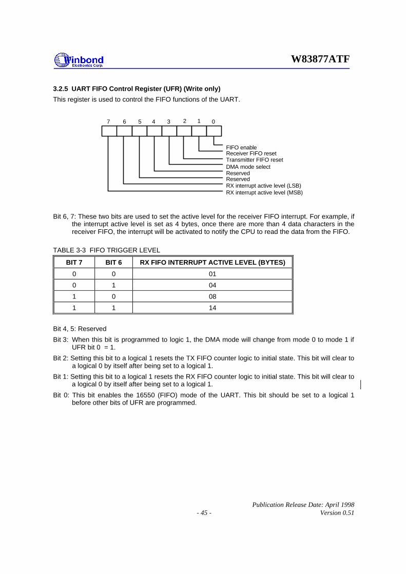
W83877ATF
Publication Release Date: April 1998 - 45 - Version 0.51
3.2.5 UART FIFO Control Register (UFR) (Write only)
This register is used to control the FIFO functions of the UART.
1234567 0
FIFO enableReceiver FIFO resetTransmitter FIFO resetDMA mode selectReservedReservedRX interrupt active level (LSB)RX interrupt active level (MSB)
Bit 6, 7: These two bits are used to set the active level for the receiver FIFO interrupt. For example, ifthe interrupt active level is set as 4 bytes, once there are more than 4 data characters in the receiver FIFO, the interrupt will be activated to notify the CPU to read the data from the FIFO.
TABLE 3-3 FIFO TRIGGER LEVEL
BIT 7 BIT 6 RX FIFO INTERRUPT ACTIVE LEVEL (BYTES)
0 0 01
0 1 04
1 0 08
1 1 14
Bit 4, 5: Reserved
Bit 3: When this bit is programmed to logic 1, the DMA mode will change from mode 0 to mode 1 if UFR bit 0 = 1.
Bit 2: Setting this bit to a logical 1 resets the TX FIFO counter logic to initial state. This bit will clear to a logical 0 by itself after being set to a logical 1.
Bit 1: Setting this bit to a logical 1 resets the RX FIFO counter logic to initial state. This bit will clear to a logical 0 by itself after being set to a logical 1.
Bit 0: This bit enables the 16550 (FIFO) mode of the UART. This bit should be set to a logical 1 before other bits of UFR are programmed.

W83877ATF
Publication Release Date: April 1998 - 46 - Version 0.51
3.2.6 Interrupt Status Register (ISR) (Read only)
This register reflects the UART interrupt status, which is encoded by different interrupt sources into 3 bits.
1234567 0
0 if interrupt pendingInterrupt Status bit 0Interrupt Status bit 1Interrupt Status bit 2FIFOs enabledFIFOs enabled
0 0
Bit 7, 6: These two bits are set to a logical 1 when UFR bit 0 = 1.
Bit 5, 4: These two bits are always logic 0.
Bit 3: In 16450 mode, this bit is 0. In 16550 mode, both bit 3 and 2 are set to a logical 1 when a time-out interrupt is pending.
Bit 2, 1: These two bits identify the priority level of the pending interrupt, as shown in the table below.
Bit 0: This bit is a logical 1 if there is no interrupt pending. If one of the interrupt sources has occurred, this bit will be set to a logical 0.
TABLE 3-4 INTERRUPT CONTROL FUNCTION
ISR INTERRUPT SET AND FUNCTION
Bit 3
Bit 2
Bit 1
Bit 0
Interrupt priority
Interrupt Type
Interrupt Source
Clear Interrupt
0 0 0 1 - - No Interrupt pending -
0 1 1 0 First UART Receive Status
1. OER = 1 2. PBER =1
3. NSER = 1 4. SBD = 1
Read USR
0 1 0 0 Second RBR Data Ready 1. RBR data ready
2. FIFO interrupt active level reached
1. Read RBR
2. Read RBR until FIFO data under active level
1 1 0 0 Second FIFO Data Timeout Data present in RX FIFO for 4 characters period of time since last access of RX FIFO.
Read RBR
0 0 1 0 Third TBR Empty TBR empty 1. Write data into TBR
2. Read ISR (if priority is third)
0 0 0 0 Fourth Handshake status 1. TCTS = 1 2. TDSR = 1
3. FERI = 1 4. TDCD = 1
Read HSR
** Bit 3 of ISR is enabled when bit 0 of UFR is logical 1.

W83877ATF
Publication Release Date: April 1998 - 47 - Version 0.51
3.2.7 Interrupt Control Register (ICR) (Read/Write) This 8-bit register allows the five types of controller interrupts to activate the interrupt output signal separately. The interrupt system can be totally disabled by resetting bits 0 through 3 of the Interrupt Control Register (ICR). A selected interrupt can be enabled by setting the appropriate bits of this register to a logical 1.
0 0 0
1234567 0
0
RBR data ready interrupt enable (ERDRI)TBR empty interrupt enable (ETBREI)UART receive status interrupt enable (EUSRI)Handshake status interrupt enable (EHSRI)
Bit 7-4: These four bits are always logic 0.
Bit 3: EHSRI. Setting this bit to a logical 1 enables the handshake status register interrupt.
Bit 2: EUSRI. Setting this bit to a logical 1 enables the UART status register interrupt.
Bit 1: ETBREI. Setting this bit to a logical 1 enables the TBR empty interrupt.
Bit 0: ERDRI. Setting this bit to a logical 1 enables the RBR data ready interrupt.
3.2.8 Programmable Baud Generator (BLL/BHL) (Read/Write)
Two 8-bit registers, BLL and BHL, compose a programmable baud generator that uses 24 MHz to
generate a 1.8461 MHz frequency and divides it by a divisor from 1 to 216-1. The output frequency of the baud generator is the baud rate multiplied by 16, and this is the base frequency for the transmitter and receiver. The table below illustrates the use of the baud generator with a frequency of 1.8461 MHz. In high-speed UART mode (refer to CR0C bit7 and CR0C bit6), the programmable baud generator directly uses 24 MHz and the same divisor as the normal speed divisor. In high-speed mode, the data transmission rate can be as high as 1.5M bps.

W83877ATF
Publication Release Date: April 1998 - 48 - Version 0.51
3.2.9 User-defined Register (UDR) (Read/Write)
This is a temporary register that can be accessed and defined by the user.
TABLE 3-5 BAUD RATE TABLE
BAUD RATE USING 24 MHZ TO GENERATE 1.8461 MHZ
Desired Baud Rate Decimal divisor used to generate 16X clock
Percent error difference between desired and actual
50 2304 **
75 1536 **
110 1047 0.18%
134.5 857 0.099%
150 768 **
300 384 **
600 192 **
1200 96 **
1800 64 **
2000 58 0.53%
2400 48 **
3600 32 **
4800 24 **
7200 16 **
9600 12 **
19200 6 **
38400 3 **
57600 2 **
115200 1 **
230400 4 Note 1 **
460800 2 Note 1 **
921600 1 Note 1 **
1.5M 1 Note 2 0%
Note 1: Only use in high speed mode, when FASTA/FASTB bits are set (refer to CR19 bit1 and CR19 bit0).
Note 2: Only use in high speed mode, when TURA/TURB bits are set (refer to CR0C bit7 and bit6).
** The percentage error for all baud rates, except where indicated otherwise, is 0.16%

W83877ATF
Publication Release Date: April 1998 - 49 - Version 0.51
3.3 IR Port
In the W83877AF includes two serial ports, that is, UART A and UART B. The second serial port, UART B, also has built-in Infrared (IR) functions which include IrDA 1.0 SIR, IrDA 1.1 MIR (1.152M bps), IrDA FIR (4M bps), SHARP ASK-IR, and remote control (that support NEC, RC-5, advanced RC-5, and RECS-80 protocol).
4.3.1 Advanced UART B Register Description
When bank select enable bit (ENBNKSEL, in CR2C.bit3) is set, UART B will be switched to Advanced UART B, and eight Register Sets can be accessed. These Register Sets control enhanced UART B, IR function switching such as SIR, MIR, or FIR. Also, a superior traditional UART B function can be used, such as 32-byte transmitter/receiver FIFO, non-encoding IRQ identify status register, and automatic flow control. The MIR/FIR and remote control registers are also defined in these Register Sets. The structure of he Register Sets is shown below.
Set 0
Reg 7
Reg 6
Reg 5
Reg 4
BDL/SSR
Reg 2
Reg 1
Reg 0
Set 1
Set 3Set 4Set 5
Set 6Set 7
Set 2
All in one Reg to Select SSR
*Set 0, 1 are legacy/Advanced UART Registers*Set 2~7 are Advanced UART Registers

W83877ATF
Publication Release Date: April 1998 - 50 - Version 0.51
All Set s registers have a common register which is Sets Select Register (SSR), in order to switch to any Set when configuring this register. The summary description of these Sets is shown below.
Set UART IR Mode
Sets Description
0 ¡ ³ ¡ ³ Legacy/Advanced UART Control and Status Registers.
1 ¡ ³ ¡ ³ Legacy Baud Rate Divisor Register.
2 ¡ ³ Advanced UART Control and Status Registers.
3 ¡ ³ Version ID and Mapped Control Registers.
4 ¡ ³ Transmitter/Receiver/Timer Counter Registers and IR Control Registers.
5 ¡ ³ Flow Control and IR Control and Frame Status FIFO Registers.
6 ¡ ³ IR Physical Layer Control Registers
7 ¡ ³ Remote Control and IR front-end Module Selection Registers.
4.3.2 Set0-Legacy/Advanced UART Control and Status Registers
Address Offset
Register Name Register Description
0 RBR/TBR Receiver/Transmitter Buffer Registers
1 ICR Interrupt Control Register
2 ISR/UFR Interrupt Status or UART FIFO Control Register
3 UCR/SSR UART Control or Sets Select Register
4 HCR Handshake Control Register
5 USR UART Status Register
6 HSR Handshake Status Register
7 UDR/ESCR User Defined Register
4.3.2.1 Set0.Reg0 - Receiver/Transmitter Buffer Registers (RBR/TBR) (Read/Write)
Receiver Buffer Register is read only and Transmitter Buffer Register is write only. These registers are described the ame as legacy UART.
In legacy UART, this port only supports PIO mode. In dvanced UART, if setup to MIR/FIR/Remote IR, this port will support DMA handshake function. Two DMA channels can be used, that is, one TX DMA channel and another RX DMA channel. Therefore, single DMA channel is also supported when the bit of D_CHSW (DMA Channel Swap, in Set2.Reg2.Bit3) is set and the TX/RX DMA channel is swapped. Note that two DMA channels are defined in config register CR2A, which selects DMA channel or disables DMA channel. If RX DMA channel is enabled and TX DMA channel is disabled, then the single DMA channel will be selected.

W83877ATF
Publication Release Date: April 1998 - 51 - Version 0.51
4.3.2.2 Set0.Reg1 - Interrupt Control Register (ICR)
Mode B7 B6 B5 B4 B3 B2 B1 B0
UART 0 0 0 0 EHSRI EUSRI ETBREI ERDRI
Advanced UART
ETMRI EFSFI ETXTHI EDMAI EHSRI EUSRI/ TXURI
ETBREI ERXTHI
Where UART is used to Legacy UART, and the functions for these bits are defined in the previous UART, the traditional SIR or ASK-IR based on the legacy UART also has the same definitions. The advanced UART functions, including Advanced SIR/ASK-IR, MIR, FIR, or Remote IR, are described as follows.
Bit 7: ETMRI - Enable Timer Interrupt
Write to 1, enable timer interrupt.
Bit 6: MIR, FIR mode:
EFSFI - Enable Frame Status FIFO Interrupt
Write to 1, enable frame status FIFO interrupt.
Advanced SIR/ASK-IR, Remote IR:
Not used.
Bit 5: Advanced SIR/ASK-IR, MIR, FIR, Remote IR:
ETXTHI - Enable Transmitter Threshold Interrupt
Write to 1, enable transmitter threshold interrupt.
Bit 4: MIR, FIR, Remote IR:
EDMAI - Enable DMA Interrupt.
Write to 1, enable DMA interrupt.
Bit 3: Advanced UART/SIR/ASK-IR, MIR, FIR, Remote IR:
EHSRI - Enable HSR (Handshake Status Register) Interrupt
Write to 1, enable handshake status register interrupt. Note that the bit IRHSSL (Infrared Handshake Select) should be set to 1, then this bit EHSRI is effective.
Bit 2: Advanced SIR/ASK-IR:
EUSRI - Enable USR (UART Status Register) Interrupt
Write to 1, enable UART status register interrupt.
MIR, FIR, Remote Controller:
EHSRI/ETXURI - Enable USR Interrupt or Enable Transmitter Underrun Interrupt
Write to 1, enable USR interrupt or enable transmitter underrun interrupt.
Bit 1: ETBREI - Enable TBR (Transmitter Buffer Register) Empty Interrupt
Write to 1, enable transmitter buffer register empty interrupt.
Bit 0: ERBRI - Enable RDR (Receiver Buffer Register) Interrupt
Write to 1, enable receiver buffer register interrupt.

W83877ATF
Publication Release Date: April 1998 - 52 - Version 0.51
4.3.2.3 Set0.Reg2 - Interrupt Status Register/UART FIFO Control Register (ISR/UFR)
(1) Interrupt Status Register: (Write Only)
Mode B7 B6 B5 B4 B3 B2 B1 B0
Legacy UART
FIFO Enable
FIFO Enable
0 0 IID2 IID1 IID0 IP
Advanced UART
TMR_I FSF_I TXTH_I DMA_I HS_I USR_I/ FEND_I
TXEMP_I RXTH_I
Reset Value 0 0 1 0 0 0 1 0
Legacy UART: Same as previous register defined. Advanced UART:
Bit 7: TMR_I - Timer Interrupt. Set to 1 when timer counts to 0. This bit will be affected by (1) the timer registers are
defined in Set4.Reg0 and Set4.Reg1, (2) EN_TMR(Enable Timer, in Set4.Reg2.Bit0) should be set to 1, (3) ENTMR_I (Enable Timer Interrupt, in Set0.Reg1.Bit7) should be set to 1.
Bit 6: MIR, FIR modes:
FSF_I - Frame Status FIFO Interrupt.
Set to 1 when Frame Status FIFO is equal to or larger than the threshold level or Frame Status FIFO time-out occurs. Clear to 0 when Frame Status FIFO is below the threshold level.
Advanced UART/SIR/ASK-IR, Remote IR modes: Not used.
Bit 5: TXTH_I - Transmitter Threshold Interrupt. Set to 1 if the TBR (Transmitter Buffer Register) FIFO is below the threshold level. Clear
to 0 if the TBR (Transmitter Buffer Register) FIFO is below the threshold level. Bit 4: MIR, FIR, Remote IR modes: DMA_I - DMA Interrupt.
Set to 1 if the DMA controller 8237A sends a TC (Terminal Count) to I/O device which may be a Transmitter TC or a Receiver TC. Clear to 0 when this register is read.
Bit 3: HS_I - Handshake Status Interrupt. Set to 1 when the Handshake Status Register has a toggle. Clear to 0 when Handshake
Status Register (HSR) is read. Note that in all IR modes including SIR, ASK-IR, MIR, FIR, and Remote Control, IR are defaulted to inactive except set IR Handshake Status Enable (IRHS_EN) to 1.
Bit 2: Advanced UART/SIR/ASK-IR modes:
USR_I - UART Status Interrupt.
Set to 1 when overrun, or parity bit, or stop bit, or silent byte detected error in the UART Status Register (USR) is set to 1. Clear to 0 when USR is read.
MIR, FIR modes:
FEND_I - Frame End Interrupt.
Set to 1 when (1) a frame has a grace end to be detected where the frame signal is defined in the physical layer of IrDA version 1.1 (2) abort signal or illegal signal has been detected during receiving valid data. Clear to 0 when this register is read.
Remote Controller mode:

W83877ATF
Publication Release Date: April 1998 - 53 - Version 0.51
Not used.
Bit 1: TXEMP_I - Transmitter Empty. Set to 1 when transmitter (or, say, FIFO + Transmitter) is empty. Clear to 0 when this
register is read. Bit 0: RXTH_I - Receiver Threshold Interrupt. Set to 1 when (1) the Receiver Buffer Register (RBR) is equal to or larger than the
threshold level, (2) RBR occurs time-out if the receiver buffer register has valid data and below the threshold level. Clear to 0 when RBR is less than threshold level from reading RBR.
(2) UART FIFO Control Register (UFR):
Mode Bit 7 Bit 6 Bit 5 Bit 4 Bit 3 Bit 2 Bit 1 Bit 0
Legacy UART
RXFTL1 (MSB)
RXFTL0 (LSB)
0 0 0 TXF_RST RXF_RST EN_FIFO
Advanced UART
RXFTL1 (MSB)
RXFTL0 (LSB)
TXFTL1 (MSB)
TXFTL0 (LSB)
0 TXF_RST RXF_RST EN_FIFO
Reset Value 0 0 0 0 0 0 0 0
Legacy UART: The definition of this register is same as Legacy UART mode. Advanced UART: Bit 7, 6: RXFTL1, 0 - Receiver FIFO Threshold Level Definition is same as Legacy UART, that is to determine the RXTH_I to become 1 when
the Receiver FIFO Threshold Level is equal or larger than the defined value shownbelow.
RXFTL1, 0 (Bit 7, 6)
RX FIFO Threshold Level (FIFO Size: 16-byte)
RX FIFO Threshold Level (FIFO Size: 32-byte)
00 1 1
01 4 4
10 8 16
11 14 26
Note that the FIFO Size is referred to SET2.Reg4.
Bit 5, 4: TXFTL1, 0 - Transmitter FIFO Threshold Level To determine the TXTH_I (Transmitter Threshold Level Interrupt) is set to 1 when the
Transmitter Threshold Level is less than the programmed value shown as follows.

W83877ATF
Publication Release Date: April 1998 - 54 - Version 0.51
TXFTL1, 0 (Bit 5, 4)
TX FIFO Threshold Level (FIFO Size: 16-byte)
TX FIFO Threshold Level (FIFO Size: 32-byte)
00 1 1
01 3 7
10 9 17
11 13 25
Bit 3 ~0 Same Legacy UART mode
4.3.2.4 Set0.Reg3 - UART Control Register/Set Select Register (UCR/SSR):
These two registers share the same address. In any Set, Set Select Register (SSR) can be programmed to desired Set, but UART Control Register can be programmed only in Set 0 and Set 1, that is, in other Sets programming this register will have no effect. The mapping of entry Set and programming value is shown as follows.
SSR Bits Selected
7 6 5 4 3 2 1 0 Hex Value Set
0 × × × × × × × ¡ Ð Set 0
1 Any value but not used in SET 2~7 ¡ Ð Set1
1 1 1 0 0 0 0 0 0xE0 Set 2
1 1 1 0 0 1 0 0 0xE4 Set 3
1 1 1 0 1 0 0 0 0xE8 Set 4
1 1 1 1 1 1 0 0 0xEC Set 5
1 1 1 1 0 0 0 0 0xF0 Set 6
1 1 1 1 0 1 0 0 0xF4 Set 7
UART Control Register: Defined legacy UART.
4.3.2.5 Set0.Reg4 - Handshake Control Register (HCR)
Mode B7 B6 B5 B4 B3 B2 B1 B0
Legacy UART
0 0 0 XLOOP EN_IRQ LP_RI RTS DTR
Advanced UART
AD_MD2 AD_MD1 AD_MD0 SIR_PLS TX_WT EN_DMA RTS DTR
Reset Value 0 0 0 0 0 0 0 0

W83877ATF
Publication Release Date: April 1998 - 55 - Version 0.51
Legacy UART Register: These registers are defined the same as in the previous description.
Advanced UART Register:
Bit 7~5 Advanced UART/SIR/ASK-IR, MIR, FIR, Remote Controller modes:
AD_MD2~0 - Advanced UART/Infrared mode Select.
These registers are active when Advanced UART Select (ADV_SL, in Set2.Reg2.Bit0) is set to 1. Operational mode selection is defined as follows. When the backward operation occurs these register will be reset to 0 and backward legacy UART mode.
AD_MD2~0 (Bit 7, 6, 5)
Selected Mode
000 Advanced UART
001 Low speed MIR (0.576M bps)
010 Advanced ASK-IR
011 Advanced SIR
100 High Speed MIR (1.152M bps)
101 FIR (4M bps)
110 Consumer IR
111 Reserved
Bit 4: MIR, FIR modes:
SIR_PLS - Send Infrared Pulse
Write to 1 then automatically sends a 2 µ s infrared pulse after physical frame end,. In order to notify SIR that the high speed infrared is still in process when this pulse is sent. This bit will be automatically cleared by hardware.
Other modes:
Not used.
Bit 3: MIR, FIR modes:
TX_WT - Transmission Waiting
If this bit sets to 1, the transmitter will wait for TX FIFO to reach threshold level or transmitter time-out which avoids short data bytes to want to transmit, before beginning to transmit data from TX FIFO. This is in order to avoid Underrun.
Other modes:
Not used.

W83877ATF
Publication Release Date: April 1998 - 56 - Version 0.51
Bit 2: MIR, FIR modes:
EN_DMA - Enable DMA
Enable DMA function to transmit or receive. Before using this, the DMA channel should be select. If RX DMA channel is set and TX DMA channel is disabled, then the single DMA channel is used. In the single channel system, the bit of D_CHSW (DMA channel swap, in Set 2.Reg2.Bit3) will determine RX DMA channel or TX DMA channel.
Other modes:
Not used.
Bit 1, 0: RTS, DTR
Functional definitions are the same as in legacy UART mode.
4.3.2.6 Set0.Reg5 - UART Status Register (USR)
Mode B7 B6 B5 B4 B3 B2 B1 B0
Legacy UART
RFEI TSRE TBRE SBD NSER PBER OER RDR
Advanced UART
LB_INFR TSRE TBRE MX_LEX PHY_ERR CRC_ERR OER RDR
Reset Value 0 0 0 0 0 0 0 0
Legacy UART Register: These registers are defined the same as in the previous description.
Advanced UART Register:
Bit 7: MIR, FIR modes:
LB_INFR - Last Byte In Frame End
Set to 1 when the last byte of a frame is in the FIFO bottom. This bit indicates that one frame is separated from another frame when RX FIFO has more than one frame.
Bit 6, 5: Same as legacy UART description.
Bit 4: MIR, FIR modes:
MX_LEX - Maximum Frame Length Exceed
Set to 1 when frame length from the receiver has exceeded the programmed frame length, which is in SET4.Reg6 and Reg5. If this bit is set to 1, the receiver will not receive any data to RX FIFO.
Bit 3: MIR, FIR modes:
PHY_ERR - Physical Layer Error
Set to 1 when an illegal data symbol is received, where the illegal data symbol is defined in physical layer of IrDA version 1.1. When this bit is set to 1, the decoder of receiver will be aborted, and a frame end signal is set to 1.

W83877ATF
Publication Release Date: April 1998 - 57 - Version 0.51
Bit 2: MIR, FIR modes:
CRC_ERR - CRC Error
Set to 1 when an attached CRC is error.
Bit 1, 0: OER - Overrun Error, RDR - RBR Data Ready
Definitions are same as for legacy UART.
4.3.2.7 Set0.Reg6 - Handshake Status Register (HSR)
Mode B7 B6 B5 B4 B3 B2 B1 B0
Legacy UART
DCD RI DSR CTS TDCD FERI TDSR TCTS
Advanced UART
DCD RI DSR CTS TDCD FERI TDSR TCTS
Reset Value 0 0 0 0 0 0 0 0
Legacy/Advanced UART Register: These registers are defined the same as in the previous description.
4.3.2.8 Set0.Reg7 - User Defined Register (UDR/AUDR)
Mode Bit 7 Bit 6 Bit 5 Bit 4 Bit 3 Bit 2 Bit 1 Bit 0
Legacy UART
Bit 7 Bit 6 Bit 5 Bit 4 Bit 3 Bit 2 Bit 1 Bit 0
Advanced UART
FLC_ACT UNDRN RX_BSY/ RX_IP
LST_FE/ RX_PD
S_FEND 0 LB_SF RX_TO
Reset Value 0 0 0 0 0 0 0 0
Legacy UART Register: These registers are defined the same as in the previous description.
Advanced UART Register:
Bit 7 MIR, FIR modes:
FLC_ACT - Flow Control Active
Set to 1 when flow control occurs. Clear to 0 when this register is read. Note that this will be affected by Set5.Reg2 which controls the SIR mode switches to MIR/FIR mode or when MIR/FIR mode operated in DMA function switches to SIR mode.
Bit 6 MIR, FIR modes:
UNDRN - Underrun
Set to 1 when transmitter is empty and not set S_FEND (in this register bit 3) operated in PIO mode or not TC (Terminal Count) operated in DMA mode. Clear to 0 when write to 1.

W83877ATF
Publication Release Date: April 1998 - 58 - Version 0.51
Bit 5 MIR, FIR modes:
RX_BSY - Receiver Busy
Set to 1 when receiver is busy or active in process.
Remote IR mode:
RX_IP - Receiver in Process
Set to 1 when receiver is in process.
Bit 4: MIR, FIR modes:
LST_FE - Lost Frame End
Set to 1 when a frame end for an entire frame is lost. Clear to 0 when read this register.
Remote IR modes:
RX_PD - Receiver Pulse Detected
Set to 1 when one or more than one remote pulses are detected. Clear to 0 when read this register.
Bit 3 MIR, FIR modes:
S_FEND - Set a Frame End
Write to 1 when wanting to terminate the frame; that is, the procedure of PIO command is
An Entire Frame = Write Frame Data (First) + Write S_FEND (Last)
This bit should be set to 1, if used in PIO mode, to avoid transmitter underrun. Note that this bit S_FEND is set to 1, that is, equivalent to TC (Terminal Count) in DMA mode. This bit should therefore be set to 0 in DMA mode.
Bit 2: Reserved.
Bit 1: MIR, FIR modes:
LB_SF - Last Byte Stay in FIFO
Set to 1 that indicates one or more than one frame end still stay in receiver FIFO.
Bit 0: MIR, FIR, Remote IR modes:
RX_TO - Receiver FIFO or Frame Status FIFO time-out
Set to 1 when receiver FIFO or frame status FIFO occurs time-out

W83877ATF
Publication Release Date: April 1998 - 59 - Version 0.51
4.3.3 Set1 - Legacy Baud Rate Divisor Register
Address Offset
Register Name Register Description
0 BLL Baud Rate Divisor Latch (Low Byte)
1 BHL Baud Rate Divisor Latch (High Byte)
2 ISR/UFR Interrupt Status or UART FIFO Control Register
3 UCR/SSR UART Control or Sets Select Register
4 HCR Handshake Control Register
5 USR UART Status Register
6 HSR Handshake Status Register
7 UDR/ESCR User Defined Register
4.3.3.1 Set1.Reg0~1 - Baud Rate Divisor Latch (BLL/BHL)
The two registers of BLL and BHL are baud rate divisor latch in the legacy UART/SIR/ASK-IR mode. Read/Write these registers, if set in Advanced UART mode, will occur backward operation, that is, will go to legacy UART mode and clear some register values shown in the table below.
Set & Register Advanced Mode DIS_BACK=×
Legacy Mode DIS_BACK=0
Set 0.Reg 4 Bit 7~5 -
Set 2.Reg 2 Bit 0, 5, 7 Bit 5, 7
Set 4.Reg 3 Bit 2, 3 -
Note that DIS_BACK=1 (Disable Backward operation) in legacy UART/SIR/ASK-IR mode will not affect any register which can operate legacy SIR/ASK-IR.
4.3.3.2 Set1.Reg 2~7
These registers are defined the same as the Set 0 registers.

W83877ATF
Publication Release Date: April 1998 - 60 - Version 0.51
4.3.4 Set2 - Interrupt Status or UART FIFO Control Register (ISR/UFR)
These registers are only used in advanced modes.
Address Offset
Register Name Register Description
0 ABLL Advanced Baud Rate Divisor Latch (Low Byte)
1 ABHL Advanced Baud Rate Divisor Latch (High Byte)
2 ADCR1 Advanced UART Control Register 1
3 SSR Sets Select Register
4 ADCR2 Advanced UART Control Register 2
5 Reserved -
6 TXFDTH Transmitter FIFO Depth
7 RXFDTH Receiver FIFO Depth
4.3.4.1 Reg0, 1 - Advanced Baud Rate Divisor Latch (ABLL/ABHL) The two registers are the same as the legacy UART baud rate divisor latch in SET 1. Reg0~1. When using advanced UART/SIR/ASK-IR mode operation, these registers should be programmed to set baud rate. This is to prevent a backward operation occurring.
4.3.4.2 Reg2 - Advanced UART Control Register 1 (ADCR1)
Mode Bit 7 Bit 6 Bit 5 Bit 4 Bit 3 Bit 2 Bit 1 Bit 0
Advanced UART
BR_OUT - EN_LOUT D_CHSW ALOOP DMATHL DMA_F ADV_SL
Reset Value 0 0 0 0 0 0 0 0
Bit 7: BR_OUT - Baud Rate Clock Output
Write to 1 enables the programmed baud rate clock to output to DTR pin. This bit is the only test baud rate divisor.
Bit 6: Reserved, write 0.
Bit 5: EN_LOUT - Enable Loopback Output
Write to 1 enables output of transmitter data to IRTX pin during doing loopback operation. Setting this bit can check output data with internal data.
Bit 4: D_CHSW - DMA TX/RX Channel Swap
If using signal DMA channel in MIR/FIR mode, then the DMA channel can be swapped.
D_CHSW DMA Channel Selected
0 Receiver (Default)
1 Transmitter
Write to 1 enables output data during the ALOOP=1.

W83877ATF
Publication Release Date: April 1998 - 61 - Version 0.51
Bit 3: ALOOP - All mode Loopback
Write to 1 enables loopback in all modes.
Bit 2: DMATHL - DMA Threshold Level
Sets DMA threshold level as shown in the table below.
DMATHL TX FIFO Threshold RX FIFO Threshold 16-Byte 32-Byte (16/32-Byte)
0 13 13 4
1 23 7 10
Bit 1: DMA_F - DMA Fairness
DMA_F Function Description
0 DMA request (DREQ) is forced inactive after 10.5us
1 No effect on DMA request.
Bit 0: ADV_SL - Advanced mode Select Write to 1 selects advanced mode.
4.3.4.3 Reg3 - Sets Select Register (SSR)
Reading this register returns E016. Write it to select other register Set.
Reg. Bit 7 Bit 6 Bit 5 Bit 4 Bit 3 Bit 2 Bit 1 Bit 0
SSR SSR7 SSR6 SSR5 SSR4 SSR3 SSR2 SRR1 SRR0
default Value 1 1 1 0 0 0 0 0
4.3.4.4 Reg4 - Advanced UART Control Register 2 (ADCR2)
Mode Bit 7 Bit 6 Bit 5 Bit 4 Bit 3 Bit 2 Bit 1 Bit 0
Advanced UART
DIS_BACK
- PR_DIV1 PR_DIV0 RX_FSZ1 RX_FSZ0 TX_FSZ1 TXFSZ0
Reset Value 0 0 0 0 0 0 0 0
Bit 7: DIS_BACK - Disable Backward Operation
Write to 1, read or write BLL or BHL (Baud rate Divisor Latch Register, in Set1.Reg0~1), will disable backward legacy UART mode. When using legacy SIR/ASK-IR mode, this bit should be set to 1 to avoid backward operation.
Bit 6: Reserved, write 0.

W83877ATF
Publication Release Date: April 1998 - 62 - Version 0.51
Bit 5, 4: PR_DIV1~0 - Pre-Divisor 1~0.
These bits select pre-divisor for external input clock 24M Hz. The clock through the pre-divisor then inputs to baud rate divisor of UART.
PR_DIV1~0 Pre-divisor Max. Baud Rate
00 13.0 115.2K bps
01 1.625 921.6K bps
10 6.5 230.4K bps
11 1 1.5M bps
Bit 3, 2: RX_FSZ1~0 - Receiver FIFO Size 1~0
These bits setup receiver FIFO size when FIFO is enabled.
RX_FSZ1~0 RX FIFO Size
00 16-Byte
01 32-Byte
1X Reserved
Bit 2, 0: TX_FSZ1~0 - Transmitter FIFO Size 1~0
These bits setup transmitter FIFO size when FIFO is enabled.
TX_FSZ1~0 TX FIFO Size
00 16-Byte
01 32-Byte
1X Reserved
4.3.4.5 Reg6 - Transmitter FIFO Depth (TXFDTH) (Read Only)
Mode Bit 7 Bit 6 Bit 5 Bit 4 Bit 3 Bit 2 Bit 1 Bit 0
Advanced UART
0 0 TXFD5 TXFD4 TXFD3 TXFD2 TXFD1 TXFD1
Reset Value 0 0 0 0 0 0 0 0

W83877ATF
Publication Release Date: April 1998 - 63 - Version 0.51
Bit 7~6: Reserved, Read 0.
Bit 5~0: Reading these bits will return the current transmitter FIFO depth, that is, how many bytes there are in the transmitter FIFO.
4.3.4.6 Reg7 - Receiver FIFO Depth (RXFDTH) (Read Only)
Mode Bit 7 Bit 6 Bit 5 Bit 4 Bit 3 Bit 2 Bit 1 Bit 0
Advanced UART
0 0 RXFD5 RXFD4 RXFD3 RXFD2 RXFD1 RXFD1
Reset Value 0 0 0 0 0 0 0 0
Bit 7~6: Reserved, Read 0.
Bit 5~0: Read these bits will return the current receiver FIFO depth, that is, how many bytes there are in the receiver FIFO.
4.3.5 Set3 - Version ID and Mapped Control Registers
Address Offset
Register Name Register Description
0 AUID Advanced UART ID
1 MP_UCR Mapped UART Control Register
2 MP_UFR Mapped UART FIFO Control Register
3 SSR Sets Select Register
4 Reversed -
5 Reserved -
6 Reserved -
7 Reserved -
4.3.5.1 Reg0 - Advanced UART ID (AUID)
This register is read only. Indicates advanced UART version ID. Read it and return 1X16.
4.3.5.2 Reg1 - Mapped UART Control Register (MP_UCR)
Read only. Reading this register that returns UART Control Register value of Set 0.

W83877ATF
Publication Release Date: April 1998 - 64 - Version 0.51
4.3.5.3 Reg2 - Mapped UART FIFO Control Register (MP_UFR)
Read only. Reading this register returns UART FIFO Control Register (UFR) value of SET 0.
4.3.5.4 Reg3 - Sets Select Register (SSR)
Reading this register returns E416. Write it to select other register Set.
Reg. Bit 7 Bit 6 Bit 5 Bit 4 Bit 3 Bit 2 Bit 1 Bit 0
SSR SSR7 SSR6 SSR5 SSR4 SSR3 SSR2 SRR1 SRR0
default Value 1 1 1 0 0 1 0 0
4.3.6 Set4 - TX/RX/Timer counter registers and IR control registers.
Address Offset
Register Name Register Description
0 TMRL Timer Value Low Byte
1 TMRH Timer Value High Byte
2 IR_MSL Infrared mode Select
3 SSR Sets Select Register
4 TFRLL Transmitter Frame Length Low Byte
5 TFRLH Transmitter Frame Length High Byte
6 RFRLL Receiver Frame Length Low Byte
7 RFRLH Receiver Frame Length High Byte
4.3.6.1 Set4.Reg0, 1 - Timer Value Register (TMRL/TMRH)
This is a 12-bit timer with resolution of 1 ms, that is, the programmed maximum time is 212-1 ms. The timer is a down-counter. The timer starts down count when the bit EN_TMR (Enable Timer) of Set4.Reg2. is set to 1. When the timer down counts to zero and EN_TMR=1, the TMR_I is set to 1. When the counter down counts to zero, a new initial value will be re-loaded into timer counter.
4.3.6.2 Set4.Reg2 - Infrared mode Select (IR_MSL)
Mode Bit 7 Bit 6 Bit 5 Bit 4 Bit 3 Bit 2 Bit 1 Bit 0
Advanced UART
- - - - IR_MSL1 IR_MSL0 TMR_TST EN_TMR
Reset Value 0 0 0 0 0 0 0 0

W83877ATF
Publication Release Date: April 1998 - 65 - Version 0.51
Bit 7~4: Reserved, write to 0.
Bit 3, 2: IR_MSL1, 0 - Infrared mode Select
Select legacy UART or SIR or ASK-IR mode. Note that using legacy SIR/ASK-IR should set DIS_BACK=1 to avoid backward operation when programming baud rate. Mode selected is shown below. Note that to avoid legacy backward operation, the bit of DIS_BACK (Disable Backward, in Set2.Reg4. Bit7) should be set to 1 when legacy ASK-IR mode or legacy SIR mode is selected.
IR_MSL1, 0 Operation Mode Selected
00 Legacy UART
01 Reserved
10 Legacy ASK-IR
11 Legacy SIR
Bit 1: TMR_TST - Timer Test Write to 1 will cause reading the TMRL/TMRH will return the programmed values of
TMRL/TMRH, that is, it does not return down count counter value. This bit is for test timer register.
Bit 0: EN_TMR - Enable Timer Write to 1 enables the timer.
4.3.6.3 Set4.Reg3 - Set Select Register (SSR)
Reading this register returns E816. A write to this register selects other Set.
Reg. Bit 7 Bit 6 Bit 5 Bit 4 Bit 3 Bit 2 Bit 1 Bit 0
SSR SSR7 SSR6 SSR5 SSR4 SSR3 SSR2 SRR1 SRR0
default Value 1 1 1 1 1 0 0 0
4.3.6.4 Set4.Reg4, 5 - Transmitter Frame Length (TFRLL/TFRLH)
Reg. Bit 7 Bit 6 Bit 5 Bit 4 Bit 3 Bit 2 Bit 1 Bit 0
TFRLL bit 7 bit 6 bit 5 bit 4 bit3 bit 2 bit 1 bit 0
Reset Value 0 0 0 0 0 0 0 0
TFRLH - - - bit 12 bit 11 bit 10 bit 9 bit 8
Reset Value - - - 0 0 0 0 0

W83877ATF
Publication Release Date: April 1998 - 66 - Version 0.51
These are 13-bit registers. A write to these registers will cause the transmitter frame length of a package be programmed. These registers are only used in APM=1 (automatic package mode, Set5.Reg4.bit5). When APM=1, the physical layer will split data stream to a programmed frame length if the transmitted data is larger than the programmed frame length. When these registers are read, they will return the number of bytes which have not been transmitted from a frame length programmed.
4.3.6.5 Set4.Reg6, 7 - Receiver Frame Length (RFRLL/RFRLH)
Reg. Bit 7 Bit 6 Bit 5 Bit 4 Bit 3 Bit 2 Bit 1 Bit 0
RFRLL bit 7 bit 6 bit 5 bit 4 bit 3 bit 2 bit 1 bit 0
Reset Value 0 0 0 0 0 0 0 0
RFRLH - - - bit 12 bit 11 bit 10 bit 9 bit 8
Reset Value - - - 0 0 0 0 0
These are 13-bit registers which combine to form a 13-bit up counter. By programming these registers, the receiver frame length will be limited to the programmed frame length. If the received frame length is larger than the programmed receiver frame length, the bit of MX_LEX (Maximum Length Exceed) will be set to 1. Simultaneously, the receiver will not receive any data to RX FIFO until the next start flag in the next frame, which is defined in the physical layer IrDA 1.1, is reached; the received data then begins to write to RX FIFO. Reading these registers will return the number of received data bytes from the receiver for a frame.
4.3.7 Set 5 - Flow control and IR control and Frame Status FIFO registers
Address Offset
Register Name Register Description
0 FCBLL Flow Control Baud Rate Divisor Latch Register (Low Byte)
1 FCBHL Flow Control Baud Rate Divisor Latch Register (High Byte)
2 FC_MD Flow Control Mode Operation
3 SSR Sets Select Register
4 IRCFG1 Infrared Config Register
5 FS_FO Frame Status FIFO Register
6 RFRLFL Receiver Frame Length FIFO Low Byte
7 RFRLFH Receiver Frame Length FIFO High Byte
4.3.7.1 Set5.Reg0, 1 - Flow Control Baud Rate Divisor Latch Register (FCDLL/ FCDHL)
If flow control occurs from MIR/FIR mode change to SIR mode, then the pre-programming baud rate of FCBLL/FCBHL is loaded to advanced baud rate divisor latch (ADBLL/ADBHL).

W83877ATF
Publication Release Date: April 1998 - 67 - Version 0.51
4.3.7.2 Set5.Reg2 - Flow Control mode Operation (FC_MD)
These registers control flow control mode operation as shown in the table below.
Reg. Bit 7 Bit 6 Bit 5 Bit 4 Bit 3 Bit 2 Bit 1 Bit 0
FC_MD FC_MD2 FC_MD1 FC_MD0 - FC_DSW EN_FD EN_BRFC EN_FC
Reset Value 0 0 0 0 0 0 0 0
Bit 7~5 FC_MD2 - Flow Control mode
When flow control state occurs, these bits will be loaded to AD_MD2~0 of advanced HSR (Handshake Status Register). These three bits are defined the same as AD_MD2~0.
Bit 4: Reserved, write 0.
Bit 3: FC_DSW - Flow Control DMA Channel Swap
Write to 1, when flow control state occurs enables DMA channel of both transmitter and receiver to be swapped.
FC_DSW Next Mode After Flow Control Occurred
0 Receiver Channel
1 Transmitter Channel
Bit 2: EN_FD - Enable Flow DMA Control
Write to 1 enables use of DMA channel when flow control has occurred.
Bit 1: EN_BRFC - Enable Baud Rate Flow Control
Write to 1 enables FC_BLL/FC_BHL (Flow Control Baud Rate Divider Latch, in Set5.Reg1~0) to be loaded to advanced baud rate divisor latch (ADBLL/ADBHL, in Set2.Reg1~0).
Bit 0: EN_FC - Enable Flow Control
Write to 1 allows use of flow control function and activation of bit 7~1 of this register.
4.3.7.3 Set5.Reg3 - Sets Select Register (SSR)
A write to this register will change Set of register. Reading this register will return EC16.
Reg. Bit 7 Bit 6 Bit 5 Bit 4 Bit 3 Bit 2 Bit 1 Bit 0
SSR SSR7 SSR6 SSR5 SSR4 SSR3 SSR2 SRR1 SRR0
default Value 1 1 1 0 1 1 0 0

W83877ATF
Publication Release Date: April 1998 - 68 - Version 0.51
4.3.7.4 Set5.Reg4 - Infrared Config Register 1 (IRCFG1)
Reg. Bit 7 Bit 6 Bit 5 Bit 4 Bit 3 Bit 2 Bit 1 Bit 0
IRCFG1 - FSF_TH FEND_M AUX_RX - - IRHSSL IR_FULL
Reset Value 0 0 0 0 0 0 0 0
Bit 7: Reserved, write 0.
Bit 6: FSF_TH - Frame Status FIFO Threshold Set this bit to determine the frame status FIFO threshold level and to generate the
FSF_I. The threshold level values are defined as follows.
FSF_TH Status FIFO Threshold Level
0 2
1 4
Bit 5: FEND_MD - Frame End mode
Write to 1 enables hardware automatically to split same length frame defined Set4.Reg4 and Set4.Reg5, i.e., TFRLL/TFRLH.
Bit 4: AUX_RX - Auxiliary Receiver Pin
Write to 1 selects IRRX input pin. (Refer to Set7.Reg7.Bit5)
Bit 3~2: Reserved, write 0.
Bit 1: IRHSSL - Infrared Handshake Status Select
Write to 0 brings the HSR (Handshake Status Register) into normal operation the same as UART. Write to 1 disables HSR; reading HSR will then return 3016.
Bit 0: IR_FULL - Infrared Full Duplex Operation
Write to 0 will cause IR function to operate in half duplex. Write to 1 will cause IR function to operate in full duplex.
4.3.7.5 Set5.Reg5 - Frame Status FIFO Register (FS_FO)
This register are indicated the FIFO bottom of frame status.
Reg. Bit 7 Bit 6 Bit 5 Bit 4 Bit 3 Bit 2 Bit 1 Bit 0
FS_FO FSFDR LST_FR - MX_LEX PHY_ERR CRC_ERR RX_OV FSF_OV
Reset Value 0 0 0 0 0 0 0 0

W83877ATF
Publication Release Date: April 1998 - 69 - Version 0.51
Bit 7: FSFDR - Frame Status FIFO Data Ready
Indicates that there is valid data in frame status FIFO bottom.
Bit 6: LST_FR - Lost Frame
Set to 1 when one or more than one frame has been lost.
Bit 5: Reserved.
Bit 4: MX_LEX - Maximum Frame Length Exceed
Set to 1 when programmed maximum frame length defined Set4.Reg6 and Set4.Reg7 are exceeded. This bit is frame status FIFO bottom. Reading this bit will return a valid value when FSFDR=1 (Frame Status FIFO Data Ready).
Bit 3: PHY_ERR - Physical Error
During receiving data, any physical layer error, defined IrDA 1.1, will be set to 1 in this bit. This bit is frame status FIFO bottom. Reading this bit will return a valid value when FSFDR=1 (Frame Status FIFO Data Ready).
Bit 2: CRC_ERR - CRC Error
Set to 1 when a bad CRC is received in a frame. This CRC belongs to physical layer defined in IrDA 1.1. This bit is frame status FIFO bottom. Reading this bit will return a valid value when FSFDR=1 (Frame Status FIFO Data Ready).
Bit 1: RX_OV - Received Data Overrun
Set to 1 when Received data in FIFO overrun occurs.
Bit 0: FSF_OV - Frame Status FIFO Overrun
Set to 1 When frame status FIFO overrun occurs.
4.3.7.5 Set5.Reg6, 7 - Receiver Frame Length FIFO (RFLFL/RFLFH) or Lost Frame Number (LST_NU)
Reg. Bit 7 Bit 6 Bit 5 Bit 4 Bit 3 Bit 2 Bit 1 Bit 0
RFLFL/ LST_NU
Bit 7 Bit 6 Bit 5 Bit 4 Bit 3 Bit 2 Bit 1 Bit 0
Reset Value 0 0 0 0 0 0 0 0
RFLFH - - - Bit 12 Bit 11 Bit 10 Bit 9 Bit 8
Reset Value 0 0 0 0 0 0 0 0
Receiver Frame Length FIFO (RFLFL/RFLFH):
These registers are 13-bit. Reading these registers will return received frame length. When read the register of RFLFH will pop-up another frame status and frame length if FSFDR=1 (Set5.Reg4.Bit7).

W83877ATF
Publication Release Date: April 1998 - 70 - Version 0.51
Lost Frame Number (LST_NU):
When LST_FR=1 (Set5.Reg4. Bit6), Reg6 is replaced to LST_NU, that is 8-bit register and read RFLFH will return 0. When read the register of RFLFH will pop-up another frame status and frame length if FSFDR=1 (Set5.Reg4.Bit7).
4.3.8 Set6 - IR Physical Layer Control Registers
Address Offset
Register Name Register Description
0 IR_CFG2 Infrared Config Register 2
1 MIR_PW MIR (1.152M bps or 0.576M bps) Pulse Width
2 SIR_PW SIR Pulse Width
3 SSR Sets Select Register
4 HIR_FNU High Speed Infrared Flag Number
5 Reserved -
6 Reserved -
7 Reserved -
4.3.8.1 Set6.Reg0 - Infrared Config Register 2 (IR_CFG2)
This register config ASK-IR, MIR, FIR operation function.
Reg. Bit 7 Bit 6 Bit 5 Bit 4 Bit 3 Bit 2 Bit 1 Bit 0
IR_CFG2 SHMD_N SHDM_N FIR_CRC MIR_CRC - INV_CRC DIS_CRC -
Reset Value 0 0 1 0 0 0 0 0
Bit 7: SHMD_N - ASK-IR Modulation Disable
SHMD_N Modulation Mode
0 SOUT modulate 500K Hz Square Wave
1 Re-rout SOUT
Bit 6: SHDM_N - ASK-IR Demodulation Disable
SHDM_N Demodulation Mode
0 Demodulation 500K Hz
1 Re-rout SIN

W83877ATF
Publication Release Date: April 1998 - 71 - Version 0.51
Bit 5: FIR_CRC - FIR (4M bps) CRC Type
FIR_CRC CRC Type
0 16-bit CRC
1 32-bit CRC
Note that the 16/32-bit CRC are defined in IrDA 1.1 physical layer.
Bit 4: MIR_CRC - MIR (1.152M/0.576M bps) CRC Type
MIR_CRC CRC Type
0 16-bit CRC
1 32-bit CRC
Bit 2: INV_CRC - Inverting CRC
Write to 1 causes CRC inverted output in physical layer.
Bit 1: DIS_CRC - Disable CRC
Write to 1 causes the transmitter not to transmit CRC in physical layer.
Bit 0: Reserved, write 1.
4.3.8.2 Set6.Reg1 - MIR (1.152M/0.576M bps) Pulse Width
Reg. Bit 7 Bit 6 Bit 5 Bit 4 Bit 3 Bit 2 Bit 1 Bit 0
MIR_PW - - - M_PW4 M_PW3 M_PW2 M_PW1 M_PW0
Reset Value 0 0 0 0 1 0 1 0
This 5-bit register is set MIR output pulse width.
M_PW4~0 MIR Pulse Width (1.152M bps)
MIR Output Width (0.576M bps)
00000 0 ns 0 ns
00001 20.83 ns 41.66 ns
00010 41.66 (==20.83*2) ns 83.32 (==41.66*2) ns
... ... ...
k10 20.83*k10 ns 41.66*k10 ns
... ... ...
11111 645 ns 1290 ns

W83877ATF
Publication Release Date: April 1998 - 72 - Version 0.51
4.3.8.3 Set6.Reg2 - SIR Pulse Width
Reg. Bit 7 Bit 6 Bit 5 Bit 4 Bit 3 Bit 2 Bit 1 Bit 0
SIR_PW - - - S_PW4 S_PW3 S_PW2 S_PW1 S_PW0
Reset Value 0 0 0 0 0 0 0 0
This 5-bit register is set SIR output pulse width.
S_PW4~0 SIR Output Pulse Width
00000 3/16 bit time of UART
01101 1.6 us
Others 1.6 us
4.3.8.4 Set6.Reg3 - Set Select Register
A write to this register will result in going to other Set. Reading this register returns F016.
Reg. Bit 7 Bit 6 Bit 5 Bit 4 Bit 3 Bit 2 Bit 1 Bit 0
SSR SSR7 SSR6 SSR5 SSR4 SSR3 SSR2 SRR1 SRR0
default Value 1 1 1 1 0 0 0 0
4.3.8.5 Set6.Reg4 - High Speed Infrared Beginning Flag Number (HIR_FNU)
Reg. Bit 7 Bit 6 Bit 5 Bit 4 Bit 3 Bit 2 Bit 1 Bit 0
HIR_FNU M_FG3 M_FG2 M_FG1 M_FG0 F_FL3 F_FL2 F_FL1 F_FL0
Reset Value 0 0 1 0 1 0 1 0
Bit 7~4: M_FG3~0 - MIR beginning Flag Number These bits define the number of transmitter Start Flag of MIR. Note that the number of
MIR start flag should be equal to or more than two which is defined in IrDA 1.1 physical layer. The default value is 2.

W83877ATF
Publication Release Date: April 1998 - 73 - Version 0.51
M_FG3~0 Beginning Flag Number
0000 Reserved
0001 1
0010 2 (Default)
0011 3
0100 4
0101 5
0110 6
0111 8
1000 10
1001 12
1010 16
1011 20
1100 24
1101 28
1110 32
1111 Reserved
Bit 3~0: F_FG3~0 - FIR Beginning Flag Number These bits define the number of transmitter Preamble Flag in FIR. Note that the number
of FIR start flag should be equal to sixteen which is defined in IrDA 1.1 physical layer. The default value is 16.
M_FG3~0 Beginning Flag Number
0000 Reserved 0001 1 0010 2 0011 3 0100 4 0101 5 0110 6 0111 8 1000 10 1001 12 1010 16 (Default) 1011 20 1100 24 1101 28 1110 32 1111 Reserved

W83877ATF
Publication Release Date: April 1998 - 74 - Version 0.51
4.3.9 Set7 - Remote control and IR module selection registers
Address Offset
Register Name Register Description
0 RIR_RXC Remote Infrared Receiver Control
1 RIR_TXC Remote Infrared Transmitter Control
2 RIR_CFG Remote Infrared Config Register
3 SSR Sets Select Register
4 IRM_SL1 Infrared Module (Front End) Select 1
5 IRM_SL2 Infrared Module Select 2
6 IRM_SL3 Infrared Module Select 3
7 IRM_CR Infrared Module Control Register
4.3.9.1 Set7.Reg0 - Remote Infrared Receiver Control (RIR_RXC)
Reg. Bit 7 Bit 6 Bit 5 Bit 4 Bit 3 Bit 2 Bit 1 Bit 0
RIR_RXC RX_FR2 RX_FR1 RX_FR0 RX_FSL4 RX_FSL3 RX_FSL2 RX_FSL1 RX_FSL0
default Value 0 0 1 0 1 0 0 1
This register defines frequency ranges of receiver remote IR.
Bit 7~5: RX_FR2~0 - Receiver Frequency Range 2~0.
These bits select the input frequency of the receiver ranges. For the input signal, that is through a band pass filter, i.e., the frequency of the input signal is located at this defined range then the signal will be received.
Bit 4~0: RX_FSL4~0 - Receiver Frequency Select 4~0.
Select the receiver operation frequency.
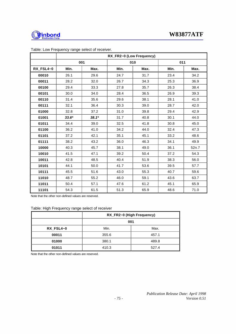
W83877ATF
Publication Release Date: April 1998 - 75 - Version 0.51
Table: Low Frequency range select of receiver.
RX_FR2~0 (Low Frequency)
001 010 011
RX_FSL4~0 Min. Max. Min. Max. Min. Max.
00010 26.1 29.6 24.7 31.7 23.4 34.2
00011 28.2 32.0 26.7 34.3 25.3 36.9
00100 29.4 33.3 27.8 35.7 26.3 38.4
00101 30.0 34.0 28.4 36.5 26.9 39.3
00110 31.4 35.6 29.6 38.1 28.1 41.0
00111 32.1 36.4 30.3 39.0 28.7 42.0
01000 32.8 37.2 31.0 39.8 29.4 42.9
01001 33.6* 38.1* 31.7 40.8 30.1 44.0
01011 34.4 39.0 32.5 41.8 30.8 45.0
01100 36.2 41.0 34.2 44.0 32.4 47.3
01101 37.2 42.1 35.1 45.1 33.2 48.6
01111 38.2 43.2 36.0 46.3 34.1 49.9
10000 40.3 45.7 38.1 49.0 36.1 52n.7
10010 41.5 47.1 39.2 50.4 37.2 54.3
10011 42.8 48.5 40.4 51.9 38.3 56.0
10101 44.1 50.0 41.7 53.6 39.5 57.7
10111 45.5 51.6 43.0 55.3 40.7 59.6
11010 48.7 55.2 46.0 59.1 43.6 63.7
11011 50.4 57.1 47.6 61.2 45.1 65.9
11101 54.3 61.5 51.3 65.9 48.6 71.0
Note that the other non-defined values are reserved.
Table: High Frequency range select of receiver
RX_FR2~0 (High Frequency)
001
RX_FSL4~0 Min. Max.
00011 355.6 457.1
01000 380.1 489.8
01011 410.3 527.4
Note that the other non-defined values are reserved.

W83877ATF
Publication Release Date: April 1998 - 76 - Version 0.51
Table: SHARP ASK-IR receiver frequency range select.
RX_FSL4~0 (SHARP ASK-IR)
RX_FR2~0
001 010 011 100 101 110
- 480.0* 533.3* 457.1 564.7 436.4 600.0 417.4 640.0 400.0 685.6 384.0 738.5
Note that the other non-defined values are reserved.
4.3.9.1 Set7.Reg1 - Remote Infrared Transmitter Control (RIR_TXC)
Reg. Bit 7 Bit 6 Bit 5 Bit 4 Bit 3 Bit 2 Bit 1 Bit 0
RIR_TXC TX_PW2 TX_PW1 TX_PW0 TX_FSL4 TX_FSL3 TX_FSL2 TX_FSL1 TX_FSL0
default Value 0 1 1 0 1 0 0 1
This Register defines the transmitter frequency and pulse width of remote IR.
Bit 7~5: TX_PW2~0 - Transmitter Pulse Width 2~ 0.
Selects the transmission pulse width.
TX_PW2~0 Low Frequency High Frequency
010 6 µ s 0.7 µ s
011 7 µ s 0.8 µ s
100 9 µ s 0.9 µ s
101 10.6 µ s 1.0 µ s
Note that the other non-defined TX_PW are reserved.
Bit 4~0: TX_FSL4~0 - Transmitter Frequency Select 4~0.
Selects the transmission frequency.
Table: Low frequency selected.
TX_FSL4~0 Low Frequency
00011 30K Hz
00100 31K HZ
... ...
11101 56K Hz
Note that the other non-defined TX_FSL4~0 are reserved.

W83877ATF
Publication Release Date: April 1998 - 77 - Version 0.51
Table: High frequency selected.
TX_FSL4~0 High Frequency
00011 400K Hz
01000 450K Hz
01011 480K Hz
Note that the other non-defined TX_FSL4~0 are reserved.
4.3.9.2 Set7.Reg2 - Remote Infrared Config Register (RIR_CFG)
Reg. Bit 7 Bit 6 Bit 5 Bit 4 Bit 3 Bit 2 Bit 1 Bit 0
RIR_CFG P_PNB SMP_M RXCFS - TX_CFS RX_DM TX_MM1 TX_MM0
default Value 0 0 0 0 0 0 0 0
Bit 7: P_PNB: Programming Pulse Number Coding. Write to 1 causes programming pulse number coding to be selected. The code format is
defined as follows.
B7 B6 B5 B4 B2 B1 B0B3
Bit value
(Number of bits) - 1
If the bit value is set to 0, then the high pulse will be transmitted/received. If the bit value
is set to 1, then no energy will be transmitted/received. Bit 6: SMP_M - Sampling mode. To choose receiver sampling mode.
Write to 0 causes T-period sampling to be used, so that the T-period is programmed UART baud rate.
Write to 1 causes direct use of programmed baud rate to do over-sampling.
Bit 5: RXCFS - Receiver Carry Frequency Select
RXCFS Selected Frequency
0 30K ~ 56K Hz
1 400K ~ 480K Hz
Bit 4: Reserved, write 0.

W83877ATF
Publication Release Date: April 1998 - 78 - Version 0.51
Bit 3: TX_CFS - Transmitter Carry Frequency Select.
Sets low speed or high speed transmitter carry frequency.
TX_FCS Selected Frequency
0 30K ~ 56K Hz
1 400K ~ 480K Hz
Bit 2: RX_DM - Receiver Demodulation mode.
RX_DM Demodulation Mode
0 Enables internal decoder
1 Disables internal decoder
Bit 1~0: TX_MM1~0 - Transmitter Modulation mode 1~0
TX_MM1~0 TX Modulation Mode
00 Continuously sends pulse for logic 0
01 8 pulses for logic 0 and no pulse for logic 1.
10 6 pulses for logic 0 and no pulse for logic 1
11 Reserved.
4.3.9.3 Set7.Reg3 - Sets Select Register (SSR)
Reg. Bit 7 Bit 6 Bit 5 Bit 4 Bit 3 Bit 2 Bit 1 Bit 0
SSR Bit 7 Bit 6 Bit 5 Bit 4 Bit 3 Bit 2 Bit 1 Bit 0
default Value 1 1 1 1 0 1 0 0
Reading this register returns F416. A write to this register causes switch to other Set.
4.3.9.4 Set7.Reg4 - Infrared Module (Front End) Select 1 (IRM_SL1)
Reg. Bit 7 Bit 6 Bit 5 Bit 4 Bit 3 Bit 2 Bit 1 Bit 0
IRM_SL1 IR_MSP SIR_SL2 SIR_SL1 SIR_SL0 - AIR_SL2 AIR_SL1 AIR_SL0
default Value 0 0 0 0 0 0 0 0

W83877ATF
Publication Release Date: April 1998 - 79 - Version 0.51
Bit 7: IR_MSP - IR mode Select Pulse
Write to 1 causes the transmitter (IRTX) to send a 64 µs pulse to setup a special IR front-end operational mode. When IR front-end module uses mode select pin (MD) and transmitter IR pulse (IRTX) to switch high speed IR (such as FIR or MIR) or low speed IR (SIR or ASK-IR), this bit should be used.
Bit 6~4: SIR_SL2~0 - SIR (Serial IR) mode select.
These bits are to program the operational mode of the SIR front-end module. These values of SIR_SL2~0 will automatically load to pins of IR_SL2~0, respectively, when (1) AM_FMT=1 (Automatic Format, in Set7.Reg7.Bit7), (2) the mode of Advanced UART is set to SIR (AD_MD2~0, in Set0.Reg4.Bit7~0).
Bit 3: Reserved, write 0.
Bit 2~0: AIR_SL2~0 - ASK-IR mode Select.
These bits will setup the operational mode of ASK-IR front-end module when AM_FMT=1 and AD_MD2~0 are set to ASK-IR mode. These values will automatically load to IR_SL2~0, respectively.
4.3.9.5 Set7.Reg5 - Infrared module (Front End) Select 2 (IRM_SL2)
Reg. Bit 7 Bit 6 Bit 5 Bit 4 Bit 3 Bit 2 Bit 1 Bit 0
IRM_SL2 - FIR_SL2 FIR_SL1 FIR_SL0 - MIR_SL2 MIR_SL1 MIR_SL0
default Value 0 0 0 0 0 0 0 0
Bit 7: Reserved, write 0.
Bit 6~4: FIR_SL2~0 - FIR mode select.
These bits setup the operational mode of FIR front-end module when AM_FMT=1 and AD_MD2~0 set to FIR mode. These values will automatically load to IR_SL2~0, respectively.
Bit 3: Reserved, write 0.
Bit 2~0: MIR_SL2~0 - MIR mode Select.
These bits setup the MIR operational mode when AM_FMT=1 and AD_MD2~0 set to MIR mode. These values will be automatically loaded to IR_SL2~0, respectively.
4.3.9.6 Set7.Reg6 - Infrared module (Front End) Select 3 (IRM_SL3)
Reg. Bit 7 Bit 6 Bit 5 Bit 4 Bit 3 Bit 2 Bit 1 Bit 0
IRM_SL3 - LRC_SL2 LRC_SL1 LRC_SL0 - HRC_SL2 HRC_SL1 HRC_SL0
default Value 0 0 0 0 0 0 0 0

W83877ATF
Publication Release Date: April 1998 - 80 - Version 0.51
Bit 7: Reserved, write 0.
Bit 6~4: LRC_SL2~0 - Low Speed Remote IR mode select.
These bits setup the operational mode of low speed remote IR front-end module when AM_FMT=1 and AD_MD2~0 set to Remote IR mode. These values will automatically load to IR_SL2~0, respectively.
Bit 3: Reserved, write 0.
Bit 2~0: HRC_SL2~0 - High Speed Remote IR Mode Select.
These bits setup the operational mode of high speed remote IR front-end module when AM_FMT=1 and .AD_MD2~0 set to Remote IR mode. These values will automatically load to IR_SL2~0, respectively.
4.3.9.7 Set7.Reg7 - Infrared module Control Register (IRM_CR)
Reg. Bit 7 Bit 6 Bit 5 Bit 4 Bit 3 Bit 2 Bit 1 Bit 0
IRM_CR AM_FMT IRX_MSL IRSL0D RXINV TXINV - - -
default Value 0 0 0 0 0 0 0 0
Bit 7: AM_FMT - Automatic Format
Write to 1 enables automatic format IR front-end module. This bit will affect the output of IR_SL2~0, which is referred by IR front-end module selection (Set7.Reg4~6)
Bit 6: IRX_MSL - IR Receiver module Select
Select the receiver input path from the IR front end module if IR module has a separated high speed and low speed receiver path. If the IR module has only one receiving path, then this bit should be set to 0.
IRX_MSL Receiver Pin selected
0 IRRX (Low/High Speed)
1 IRRXH (High Speed)
Bit 5: IRSL0D - Direction of IRSL0 Pin
Select function for IRRXH or IRSL0 because they share a common pin with different input/output direction.
IRSL0_D Function
0 IRRXH (I/P)
1 IRSL0 (O/P)

W83877ATF
Publication Release Date: April 1998 - 81 - Version 0.51
Table: IR receiver input pin selection
IRSL0D IRX_MSL AUX_RX High Speed IR Selected IR Pin
0 0 0 X IRRX
0 0 1 X IRRXH
0 1 X 0 IRRX
0 1 X 1 IRRXH
1 0 0 X IRRX
1 0 1 X Reserved
1 1 X 0 IRRX
1 1 X 1 Reserved
Note that (1) AUX_RX is defined in Set5.Reg4.Bit4, (2) high speed IR includes MIR (1.152M or 0.576M bps) and FIR (4M bps), (3) IRRX is the input of the low speed or high speed IR receiver, IRRXH is the input of the high speed IR receiver.
Bit 4: RXINV - Receiving Signal Invert
Write to 1 inverts the receiving signal.
Bit 3: TXINV - Transmitting Signal Invert
Write to 1 inverts the transmitting signal.
Bit 2~0: Reserved, write 0.

W83877ATF
Publication Release Date: April 1998 - 82 - Version 0.51
4.0 PARALLEL PORT
4.1 Printer Interface Logic
The parallel port of the W83877ATF makes possible the attachment of various devices that accept eight bits of parallel data at standard TTL level. The W83877ATF supports an IBM XT/AT compatible parallel port (SPP), bi-directional parallel port (BPP), Enhanced Parallel Port (EPP), Extended Capabilities Parallel Port (ECP), Extension FDD mode (EXTFDD), and Extension 2FDD mode (EXT2FDD) on the parallel port. Refer to the configuration registers for more information on disabling, power-down, and on selecting the mode of operation.
Table 4-1 shows the pin definitions for different modes of the parallel port.
TABLE 4-1-A Parallel Port Connnector and Pin Definition for SPP/EPP/ECP Modes
HOST CONNECTOR
PIN NUMBER OF W83877ATF
PIN ATTRIBUTE
SPP EPP ECP
1 19 O nSTB nWrite nSTB, HostClk
2-9 9-14,16-17 I/O PD<0:7> PD<0:7> PD<0:7>
10 26 I nACK Intr nACK, PeriphClk
11 24 I BUSY nWait BUSY, PeriphAck2
12 27 I PE PE PEerror, nAckReverse2
13 28 I SLCT Select SLCT, Xflag
14 20 O nAFD nDStrb nAFD, HostAck2
15 29 I nERR nError nFault1, nPeriphRequest2
16 21 O nINIT nInit nINIT1, nReverseRqst2
17 22 O nSLIN nAStrb nSLIN1 , ECPMode2
Notes:
n<name > : Active Low
1. Compatible Mode
2. High Speed Mode
3. For more information, refer to the IEEE 1284 standard.

W83877ATF
Publication Release Date: April 1998 - 83 - Version 0.51
TABLE 4-1-B Parallel Port Connector and Pin Definition for EXTFDD and EXT2FDD Modes
HOST CONNECTOR
PIN NUMBER OF W83877ATF
PIN ATTRIBUTE
SPP PIN ATTRIBUTE
EXT2FDD PIN ATTRIBUTE
EXTFDD
1 19 O nSTB --- --- --- ---
2 9 I/O PD0 I INDEX2 I INDEX2
3 10 I/O PD1 I TRAK02 I
4 11 I/O PD2 I WP2 I
5 12 I/O PD3 I RDATA2 I RDATA2
6 13 I/O PD4 I DSKCHG2 I DSKCHG2
7 14 I/O PD5 --- --- --- ---
8 15 I/O PD6 OD MOA2 --- ---
9 16 I/O PD7 OD DSA2 --- ---
10 26 I nACK OD DSB2 OD
11 24 I BUSY OD MOB2 OD
12 27 I PE OD WD2 OD WD2
13 28 I SLCT OD WE2 OD WE2
14 20 O nAFD OD RWC2 OD RWC2
15 29 I nERR OD NERR2 OD
16 21 O nINIT OD DIR2 OD DIR2
17 22 O nSLIN OD STEP2 OD

W83877ATF
Publication Release Date: April 1998 - 84 - Version 0.51
4.2 Enhanced Parallel Port (EPP)
TABLE 4-2 PRINTER MODE AND EPP REGISTER ADDRESS
A2 A1 A0 REGISTER NOTE
0 0 0 Data port (R/W) 1
0 0 1 Printer status buffer (Read) 1
0 1 0 Printer control latch (Write) 1
0 1 0 Printer control swapper (Read) 1
0 1 1 EPP address port (R/W) 2
1 0 0 EPP data port 0 (R/W) 2
1 0 1 EPP data port 1 (R/W) 2
1 1 0 EPP data port 2 (R/W) 2
1 1 1 EPP data port 2 (R/W) 2
Notes:
1. These registers are available in all modes.
2. These registers are available only in EPP mode.
4.2.1 Data Swapper
The system microprocessor can read the contents of the printer's data latch by reading the data swapper.
4.2.2 Printer Status Buffer
The system microprocessor can read the printer status by reading the address of the printer status buffer. The bit definitions are as follows:
1
1 1
235 467 0
TMOUTERRORSLCTPE
BUSY
ACK
Bit 7: This signal is active during data entry, when the printer is off-line during printing, when the print head is changing position, or during an error state. When this signal is active, the printer is busy and cannot accept data.
Bit 6: This bit represents the current state of the printer's ACK signal. A 0 means the printer has received a character and is ready to accept another. Normally, this signal will be active for
approximately 5 microseconds before BUSY stops.
Bit 5: A 1 means the printer has detected the end of paper.

W83877ATF
Publication Release Date: April 1998 - 85 - Version 0.51
Bit 4: A 1 means the printer is selected.
Bit 3: A 0 means the printer has encountered an error condition.
Bit 1, 2: These two bits are not implemented and are logic one during a read of the status register.
Bit 0: This bit is valid in EPP mode only. It indicates that a 10 µS time-out has occurred on the EPP bus. A logic 0 means that no time-out error has occurred; a logic 1 means that a time-out error has been detected. Writing a logic 1 to this bit will clear the time-out status bit; writing a logic 0 has no effect.
4.2.3 Printer Control Latch and Printer Control Swapper
The system microprocessor can read the contents of the printer control latch by reading the printer control swapper. Bit definitions are as follows:
1
1
1
234567 0
STROBEAUTO FD
SLCT INIRQ ENABLEDIR
INIT
Bit 7, 6: These two bits are a logic one during a read. They can be written.
Bit 5: Direction control bit
When this bit is a logic 1, the parallel port is in input mode (read); when it is a logic 0, the parallel port is in output mode (write). This bit can be read and written. In SPP mode, this bit is invalid and fixed at zero.
Bit 4: A 1 in this position allows an interrupt to occur when ACK changes from low to high.
Bit 3: A 1 in this bit position selects the printer.
Bit 2: A 0 starts the printer (50 microsecond pulse, minimum).
Bit 1: A 1 causes the printer to line-feed after a line is printed.
Bit 0: A 0.5 microsecond minimum high active pulse clocks data into the printer. Valid data must be present for a minimum of 0.5 microseconds before and after the strobe pulse.

W83877ATF
Publication Release Date: April 1998 - 86 - Version 0.51
4 .2.4 EPP Address Port
The address port is available only in EPP mode. Bit definitions are as follows:
1234567 0
PD0PD1PD2PD3
PD5PD4
PD6PD7
The contents of DB0-DB7 are buffered (non-inverting) and output to ports PD0-PD7 during a write
operation. The leading edge of IOW causes an EPP address write cycle to be performed, and the
trailing edge of IOW latches the data for the duration of the EPP write cycle.
PD0-PD7 ports are read during a read operation. The leading edge of IOR causes an EPP address read cycle to be performed and the data to be output to the host CPU.
4.2.5 EPP Data Port 0-3
These four registers are available only in EPP mode. Bit definitions of each data port are as follows:
1234567 0
PD0PD1PD2PD3PD4PD5PD6PD7
When accesses are made to any EPP data port, the contents of DB0-DB7 are buffered (non-inverting) and output to the ports PD0-PD7 during a write operation. The leading edge of IOW causes an EPP data write cycle to be performed, and the trailing edge of IOW latches the data for the duration of the EPP write cycle.
During a read operation, ports PD0-PD7 are read, and the leading edge of IOR causes an EPP read cycle to be performed and the data to be output to the host CPU.

W83877ATF
Publication Release Date: April 1998 - 87 - Version 0.51
4 .2.6 Bit Map of Parallel Port and EPP Registers
REGISTER 7 6 5 4 3 2 1 0
Data Port (R/W) PD7 PD6 PD5 PD4 PD3 PD2 PD1 PD0
Status Buffer (Read) BUSY ACK PE SLCT ERROR 1 1 TMOUT
Control Swapper (Read) 1 1 1 IRQEN SLIN INIT AUTOFD STROBE
Control Latch (Write) 1 1 DIR IRQ SLIN INIT AUTOFD STROBE
EPP Address Port (R/W)
PD7 PD6 PD5 PD4 PD3 PD2 PD1 PD0
EPP Data Port 0 (R/W) PD7 PD6 PD5 PD4 PD3 PD2 PD1 PD0
EPP Data Port 1 (R/W) PD7 PD6 PD5 PD4 PD3 PD2 PD1 PD0
EPP Data Port 2 (R/W) PD7 PD6 PD5 PD4 PD3 PD2 PD1 PD0
EPP Data Port 3 (R/W) PD7 PD6 PD5 PD4 PD3 PD2 PD1 PD0
4.2.7 EPP Pin Descriptions
EPP NAME TYPE EPP DESCRIPTION
nWrite O Denotes an address or data read or write operation.
PD<0:7> I/O Bi-directional EPP address and data bus.
Intr I Used by peripheral device to interrupt the host.
nWait I Inactive to acknowledge that data transfer is completed. Active to indicate that the device is ready for the next transfer.
PE I Paper end; same as SPP mode.
Select I Printer selected status; same as SPP mode.
nDStrb O This signal is active low. It denotes a data read or write operation.
nError I Error; same as SPP mode.
nInits O This signal is active low. When it is active, the EPP device is reset to its initial operating mode.
nAStrb O This signal is active low. It denotes an address read or write operation.
4.2.8 EPP Operation
When the EPP mode is selected in the configuration register, the standard and bi-directional modes are also available. The PDx bus is in the standard or bi-directional mode when no EPP read, write, or address cycle is currently being executed. In this condition all output signals are set by the SPP Control Port and the direction is controlled by DIR of the Control Port.
A watchdog timer is required to prevent system lockup. The timer indicates that more than 10 µS have elapsed from the start of the EPP cycle to the time WAIT is de-asserted. The current EPP cycle is aborted when a time-out occurs. The time-out condition is indicated in Status bit 0.

W83877ATF
Publication Release Date: April 1998 - 88 - Version 0.51
EPP Operation
The EPP operates on a two-phase cycle. First, the host selects the register within the device for subsequent operations. Second, the host performs a series of read and/or write byte operations to the selected register. Four operations are supported on the EPP: Address Write, Data Write, Address Read, and Data Read. All operations on the EPP device are performed asynchronously.
EPP Version 1.9 Operation
The EPP read/write operation can be completed under the following conditions:
a. If the nWait is active low, when the read cycle (nWrite inactive high, nDStrb/nAStrb active low) or write cycle (nWrite active low, nDStrb/nAStrb active low) starts, the read/write cycle proceeds normally and will be completed when nWait goes inactive high.
b. If nWait is inactive high, the read/write cycle will not start. It must wait until nWait changes to active low, at which time it will start as described above.
EPP Version 1.7 Operation
The EPP read/write cycle can start without checking whether nWait is active or inactive. Once the read/write cycle starts, however, it will not terminate until nWait changes from active low to inactive high.
4.3 Extended Capabilities Parallel (ECP) Port
This port is software and hardware compatible with existing parallel ports, so it may be used in a standard printer mode if ECP is not required. It provides an automatic high burst-bandwidth channel that supports DMA for ECP in both the forward (host to peripheral) and reverse (peripheral to host) directions.
Small FIFOs are used in both forward and reverse directions to improve the maximum bandwidth requirement. The size of the FIFO is 16 bytes. The ECP port supports an automatic handshake for the standard parallel port to improve compatibility mode transfer speed.
The ECP port supports run-length-encoded (RLE) decompression (required) in the hardware. Compression is accomplished by counting identical bytes and transmitting an RLE byte that indicates how many times the next byte is to be repeated. The hardware support for compression is optional.
For more information about the ECP Protocol, refer to the Extended Capabilities Port Protocol and ISA Interface Standard.

W83877ATF
Publication Release Date: April 1998 - 89 - Version 0.51
4.3.1 ECP Register and Mode Definitions
NAME ADDRESS I/O ECP MODES FUNCTION
data Base+000h R/W 000-001 Data Register
ecpAFifo Base+000h R/W 011 ECP FIFO (Address)
dsr Base+001h R All Status Register
dcr Base+002h R/W All Control Register
cFifo Base+400h R/W 010 Parallel Port Data FIFO
ecpDFifo Base+400h R/W 011 ECP FIFO (DATA)
tFifo Base+400h R/W 110 Test FIFO
cnfgA Base+400h R 111 Configuration Register A
cnfgB Base+401h R/W 111 Configuration Register B
ecr Base+402h R/W All Extended Control Register
Note: The base addresses are specified by CR23, which are determined by configuration register or hardware setting.
MODE DESCRIPTION
000 SPP mode
001 PS/2 Parallel Port mode
010 Parallel Port Data FIFO mode
011 ECP Parallel Port mode
100 EPP mode (If this option is enabled in the CR9 and CR0 to select ECP/EPP mode)
101 Reserved
110 Test mode
111 Configuration mode
Note: The mode selection bits are bit 7-5 of the Extended Control Register.
4.3.2 Data and ecpAFifo Port
Modes 000 (SPP) and 001 (PS/2) (Data Port)
During a write operation, the Data Register latches the contents of the data bus on the rising edge of the input. The contents of this register are output to the PD0-PD7 ports. During a read operation, ports PD0-PD7 are read and output to the host. The bit definitions are as follows:

W83877ATF
Publication Release Date: April 1998 - 90 - Version 0.51
7 6 5 4 3 2 1 0
PD0PD1PD2PD3PD4PD5PD6PD7
Mode 011 (ECP FIFO-Address/RLE)
A data byte written to this address is placed in the FIFO and tagged as an ECP Address/RLE. The hardware at the ECP port transmits this byte to the peripheral automatically. The operation of this register is defined only for the forward direction. The bit definitions are as follows:
7 6 5 4 3 2 1 0
Address or RLE
Address/RLE
4.3.3 Device Status Register (DSR)
These bits are at low level during a read of the Printer Status Register. The bits of this status register are defined as follows:
7 6 5 4 3 2 1 0
nFaultSelectPErrornAcknBusy
11 1
Bit 7: This bit reflects the complement of the Busy input.
Bit 6: This bit reflects the nAck input.
Bit 5: This bit reflects the PError input.
Bit 4: This bit reflects the Select input.
Bit 3: This bit reflects the nFault input.
Bit 2-0: These three bits are not implemented and are always logic one during a read.

W83877ATF
Publication Release Date: April 1998 - 91 - Version 0.51
4.3.4 Device Control Register (DCR)
The bit definitions are as follows:
7 6 5 4 3 2 1 0
1 1
StrobeAutofdnInitSelect In
DirectionAckInt En
Bit 6, 7: These two bits are logic one during a read and cannot be written.
Bit 5: This bit has no effect and the direction is always out if mode = 000 or mode = 010. Direction is valid in all other modes.
0 the parallel port is in output mode.
1 the parallel port is in input mode.
Bit 4: Interrupt request enable. When this bit is set to a high level, it may be used to enable interrupt requests from the parallel port to the CPU due to a low to high transition on the ACK input.
Bit 3: This bit is inverted and output to the SLIN output.
0 The printer is not selected.
1 The printer is selected.
Bit 2: This bit is output to the INIT output.
Bit 1: This bit is inverted and output to the AFD output.
Bit 0: This bit is inverted and output to the STB output.
4.3.5 cFifo (Parallel Port Data FIFO) Mode = 010
This mode is defined only for the forward direction. The standard parallel port protocol is used by a hardware handshake to the peripheral to transmit bytes written or DMAed from the system to this FIFO. Transfers to the FIFO are byte aligned.
4.3.6 ecpDFifo (ECP Data FIFO) Mode = 011
When the direction bit is 0, bytes written or DMAed from the system to this FIFO are transmitted by a hardware handshake to the peripheral using the ECP parallel port protocol. Transfers to the FIFO are byte aligned.
When the direction bit is 1, data bytes from the peripheral are read under automatic hardware handshake from ECP into this FIFO. Reads or DMAs from the FIFO will return bytes of ECP data to the system.

W83877ATF
Publication Release Date: April 1998 - 92 - Version 0.51
4.3.7 tFifo (Test FIFO Mode) Mode = 110
Data bytes may be read, written, or DMAed to or from the system to this FIFO in any direction.
Data in the tFIFO will not be transmitted to the parallel port lines. However, data in the tFIFO may be displayed on the parallel port data lines.
4.3.8 cnfgA (Configuration Register A) Mode = 111
This register is a read-only register. When it is read, 10H is returned. This indicates to the system that this is an 8-bit implementation.
4.3.9 cnfgB (Configuration Register B) Mode = 111
The bit definitions are as follows:
7 6 5 4 3 2 1 0
1 1 1
intrValuecompress
IRQx 0IRQx 1IRQx 2
Bit 7: This bit is read-only. It is at low level during a read. This means that this chip does not support hardware RLE compression.
Bit 6: Returns the value on the ISA IRQ line to determine possible conflicts.
Bit 5-3: Reflect the IRQ resource assigned for ECP port.
cnfgB[5:3] IRQ resource 000 reflect other IRQ resources selected by PnP register (default) 001 IRQ7 010 IRQ9 011 IRQ10 100 IRQ11 101 IRQ14 110 IRQ15 111 IRQ5
Bit 2-0: These five bits are at high level during a read and can be written.

W83877ATF
Publication Release Date: April 1998 - 93 - Version 0.51
4.3.10 ecr (Extended Control Register) Mode = all This register controls the extended ECP parallel port functions. The bit definitions are follows:
7 6 5 4 3 2 1 0
EmptyFullService IntrDMA EnnErrIntr EnMODEMODEMODE
Bit 7-5: These bits are read/write and select the mode.
000 Standard Parallel Port mode. The FIFO is reset in this mode.
001 PS/2 Parallel Port mode. This is the same as 000 except that direction may be used to tri-state the data lines, and reading the data register returns the value on the data lines and not the value in the data register.
010 Parallel Port FIFO mode. This is the same as 000 except that bytes are written or DMAed to the FIFO. FIFO data are automatically transmitted using the standard parallel port protocol. This mode is useful only when direction is 0.
011 ECP Parallel Port Mode. When the direction is 0 (forward direction), bytes placed into the ecpDFifo and bytes written to the ecpAFifo are placed in a single FIFO and transmitted automatically to the peripheral using ECP Protocol. When the direction is 1 (reverse direction) bytes are moved from the ECP parallel port and packed into bytes in the ecpDFifo.
100 Selects EPP Mode. In this mode, EPP is active if the EPP supported option is selected.
101 Reserved.
110 Test Mode. The FIFO may be written and read in this mode, but the data will not be transmitted on the parallel port.
111 Configuration Mode. The confgA and confgB registers are accessible at 0x400 and 0x401 in this mode.
Bit 4: Read/Write (Valid only in ECP Mode)
1 Disables the interrupt generated on the asserting edge of nFault.
0 Enables an interrupt pulse on the high to low edge of nFault. If nFault is asserted (interrupt) an interrupt will be generated and this bit is written from a 1 to 0.
Bit 3: Read/Write
1 Enables DMA. 0 Disables DMA unconditionally.

W83877ATF
Publication Release Date: April 1998 - 94 - Version 0.51
Bit 2: Read/Write
1 Disables DMA and all of the service interrupts. 0 Enables one of the following cases of interrupts. When one of the service interrupts
has occurred, the serviceIntr bit is set to a 1 by hardware. This bit must be reset to 0 to re-enable the interrupts. Writing a 1 to this bit will not cause an interrupt. (a) dmaEn = 1: During DMA this bit is set to a 1 when terminal count is reached. (b) dmaEn = 0 direction = 0: This bit is set to 1 whenever there are writeIntr Threshold or more bytes free in the FIFO. (c) dmaEn = 0 direction = 1: This bit is set to 1 whenever there are readIntr Threshold or more valid bytes to be read from the FIFO.
Bit 1: Read only
0 The FIFO has at least 1 free byte. 1 The FIFO cannot accept another byte or the FIFO is completely full.
Bit 0: Read only
0 The FIFO contains at least 1 byte of data. 1 The FIFO is completely empty.
4.3.11 Bit Map of ECP Port Registers
D7 D6 D5 D4 D3 D2 D1 D0 NOTE
data PD7 PD6 PD5 PD4 PD3 PD2 PD1 PD0
ecpAFifo Addr/RLE Address or RLE field 2
dsr nBusy nAck PError Select nFault 1 1 1 1
dcr 1 1 Directio ackIntEn SelectIn nInit autofd strobe 1
cFifo Parallel Port Data FIFO 2
ecpDFifo ECP Data FIFO 2
tFifo Test FIFO 2
cnfgA 0 0 0 1 0 0 0 0
cnfgB compress intrValue 1 1 1 1 1 1
ecr MODE nErrIntrEn dmaEn serviceIntr full empty
Notes:
1. These registers are available in all modes.
2. All FIFOs use one common 16-byte FIFO.

W83877ATF
Publication Release Date: April 1998 - 95 - Version 0.51
4 .3.12 ECP Pin Descriptions
NAME TYPE DESCRIPTION
nStrobe (HostClk) O The nStrobe registers data or address into the slave on the asserting edge during write operations. This signal handshakes with Busy.
PD<7:0> I/O These signals contains address or data or RLE data.
nAck (PeriphClk) I This signal indicates valid data driven by the peripheral when asserted. This signal handshakes with nAutofd in reverse.
Busy (PeriphAck) I This signal deasserts to indicate that the peripheral can accept data. It indicates whether the data lines contain ECP command information or data in the reverse direction. When in reverse direction, normal data are transferred when Busy (PeriphAck) is high and an 8-bit command is transferred when it is low.
PError (nAckReverse) I This signal is used to acknowledge a change in the direction of the transfer (asserted = forward). The peripheral drives this signal low to acknowledge nReverseRequest. The host relies upon nAckReverse to determine when it is permitted to drive the data bus.
Select (Xflag) I Indicates printer on line.
nAutoFd (HostAck) O Requests a byte of data from the peripheral when it is asserted. This signal indicates whether the data lines contain ECP address or data in the forward direction. When in forward direction, normal data are transferred when nAutoFd (HostAck) is high and an 8-bit command is transferred when it is low.
nFault (nPeriphRequest) I Generates an error interrupt when it is asserted. This signal is valid only in the forward direction. The peripheral is permitted (but not required) to drive this pin low to request a reverse transfer during ECP Mode.
nInit (nReverseRequest) O This signal sets the transfer direction (asserted = reverse, deasserted = forward). This pin is driven low to place the channel in the reverse direction.
nSelectIn (ECPMode) O This signal is always deasserted in ECP mode.

W83877ATF
Publication Release Date: April 1998 - 96 - Version 0.51
4.3.13 ECP Operation
The host must negotiate on the parallel port to determine if the peripheral supports the ECP protocol before ECP operation. After negotiation, it is necessary to initialize some of the port bits. The following are required:
(a) Set direction = 0, enabling the drivers.
(b) Set strobe = 0, causing the nStrobe signal to default to the deasserted state.
(c) Set autoFd = 0, causing the nAutoFd signal to default to the deasserted state.
(d) Set mode = 011 (ECP Mode) ECP address/RLE bytes or data bytes may be sent automatically by writing the ecpAFifo or ecpDFifo, respectively.
Mode Switching
Software will execute P1284 negotiation and all operation prior to a data transfer phase under programmed I/O control (mode 000 or 001). Hardware provides an automatic control line handshake, moving data between the FIFO and the ECP port only in the data transfer phase (mode 011 or 010).
If the port is in mode 000 or 001, it may switch to any other mode. If the port is not in mode 000 or 001, it can only be switched into mode 000 or 001. The direction can be changed only in mode 001.
When in extended forward mode, the software should wait for the FIFO to be empty before switching back to mode 000 or 001. In ECP reverse mode the software waits for all the data to be read from the FIFO before changing back to mode 000 or 001.
Command/Data
ECP mode allows the transfer of normal 8-bit data or 8-bit commands. In the forward direction, normal data are transferred when HostAck is high and an 8-bit command is transferred when HostAck is low. The most significant bits of the command indicate whether it is a run-length count (for compression) or a channel address.
In the reverse direction, normal data are transferred when PeriphAck is high and an 8-bit command is transferred when PeriphAck is low. The most significant bit of the command is always zero.
Data Compression
The W83877ATF supports run length encoded (RLE) decompression in hardware and can transfer compressed data to a peripheral. Note that odd (RLE) compression in hardware is not supported. In order to transfer data in ECP mode, the compression count is written to the ecpAFifo and the data byte is written to the ecpDFifo.
4.3.14 FIFO Operation
The FIFO threshold is set in configuration register 5. All data transfers to or from the parallel port can proceed in DMA or Programmed I/O (non-DMA) mode, as indicated by the selected mode. The FIFO is used by selecting the Parallel Port FIFO mode or ECP Parallel Port Mode. After a reset, the FIFO is disabled.

W83877ATF
Publication Release Date: April 1998 - 97 - Version 0.51
4.3.15 DMA Transfers
DMA transfers are always to or from the ecpDFifo, tFifo, or CFifo. The DMA uses the standard PC DMA services. The ECP requests DMA transfers from the host by activating the PDRQ pin. The DMA will empty or fill the FIFO using the appropriate direction and mode. When the terminal count in the DMA controller is reached, an interrupt is generated and serviceIntr is asserted, which will disable the DMA.
4.3.16 Programmed I/O (NON-DMA) Mode
The ECP or parallel port FIFOs can also be operated using interrupt driven programmed I/O. Programmed I/O transfers are to the ecpDFifo at 400H and ecpAFifo at 000H, or from the ecpDFifo located at 400H, or to/from the tFifo at 400H. The host must set the direction, state, dmaEn = 0 and serviceIntr = 0 in the programmed I/O transfers.
The ECP requests programmed I/O transfers from the host by activating the IRQ pin. The programmed I/O will empty or fill the FIFO using the appropriate direction and mode. 4.4 Extension FDD Mode (EXTFDD)
In this mode, the W83877ATF changes the printer interface pins to FDC input/output pins, allowing the user to install a second floppy disk drive (FDD B) through the DB-25 printer connector. The pin assignments for the FDC input/output pins are shown in Table 5-1.
After the printer interface is set to EXTFDD mode, the following occur:
(1) Pins MOB and DSB will be forced to inactive state.
(2) Pins DSKCHG, RDATA, WP, TRAK0, INDEX will be logically ORed with pins PD4-PD0 to serve as input signals to the FDC.
(3) Pins PD4-PD0 each will have an internal resistor of about 1K ohm to serve as pull-up resistor for FDD open drain/collector output.
(4) If the parallel port is set to EXTFDD mode after the system has booted DOS or another operating system, a warm reset is needed to enable the system to recognize the extension floppy drive.
4.5 Extension 2FDD Mode (EXT2FDD)
In this mode, the W83877ATF changes the printer interface pins to FDC input/output pins, allowing the user to install two external floppy disk drives through the DB-25 printer connector to replace internal floppy disk drives A and B. The pin assignments for the FDC input/output pins are shown in Table 5-1.
After the printer interface is set to EXTFDD mode, the following occur:
(1) Pins MOA , DSA, MOB, and DSB will be forced to inactive state.
(2) Pins DSKCHG, RDATA, WP, TRAK0, and INDEX will be logically ORed with pins PD4-PD0 to serve as input signals to the FDC.
(3) Pins PD4-PD0 each will have an internal resistor of about 1K ohm to serve as pull-up resistor for FDD open drain/collector output.
(4) If the parallel port is set to EXT2FDD mode after the system has booted DOS or another operating system, a warm reset is needed to enable the system to recognize the extension floppy drive.

W83877ATF
Publication Release Date: April 1998 - 98 - Version 0.51
5.0 PLUG AND PLAY CONFIGURATION
A powerful new plug-and-play function has been built into the W83877ATF to help simplify the task of setting up a computer environment. With appropriate support from BIOS manufacturers, the system designer can freely allocate Winbond I/O devices (i.e., the FDC, PRT and UART ) in the PC's I/O space (100H - 3FFH). In addition, the W83877ATF also provides 8 interrupt requests and 3 DMA pairs for designers to assign in interfacing FDCs, UARTs, and PRTs. Hence this powerful I/O chip offers greater flexibility for system designers.
The PnP feature is implemented through a set of Extended Function Registers (CR20 to 29). Details on configuring these registers are given in Section 8. The default values of these PnP-related registers set the system to a configuration compatible with environments designed with previous Winbond I/O chips.
6.0 ACPI /LEGACY FEATURE AND AUTO POWER MANAGEMENT
6.1 ACPI/Legacy power management
W83877ATF supports both ACPI and legacy power management models. For the ACPI power
management, the SCI pin is dedicated to the SCI interrupt signal for the SCI interrupt handler; For
the legacy power management, the SMI pin is dedicated to the SMI interrupt signal for the SMI interrupt handler.
Two register blocks are used for the ACPI/Legacy power management. They are the PM1 and GPE register blocks. Their base addresses are held in the W83877ATF configuration registers CR33 and CR34 respectively. Configuration registers CR40 to CR45 are for the legacy power management. The above configuration registers hold the interrupt event enable and status bits of the SMI interrupts. Control over the routing of SCI and SMI interrupts to the output pins is also contained in the above registers.
One 24-bit power management timer is also implemented. It provides an accurate time value used by the system software to measure and profile system idleness.
6.2 Device(auto) power management
W83877ATF also provides the auto power management function for each device within it. They are the printer port, FDC, UART A, and UART B devices in W83877ATF respectively. Device idle and trap status are provided to indicate the device's working/sleeping state. Device idle timer with programmable initial value is provided for each device, which enters the powerdown state when the powerdown conditions are met. Any access to certain registers and external event input will wake up the devices. The global stand-by timer deals with the other logic part excluding the printer port, FDC, UART A , and UART B devices. The global stand-by timer reloads and counts down as soon as the 4 devices enter the powerdown mode and W83877ATF enters the powerdown mode as soon as it expires. Once any device is awakened, the global stand-by is also awakened. The initial count values of the devices are held in the configuration registers CR35 to CR39.

W83877ATF
Publication Release Date: April 1998 - 99 - Version 0.51
7.0 SERIAL IRQ
W83877ATF supports a serial IRQ scheme. This allows a signal line to be used to report the legacy ISA interrupt requests. Because more than one device may need to share the signal serial IRQ signal line, an open drain signal scheme is used. The clock source is the PCI clock. The serial interrupt is transfered on the IRQSER signal, one cycle consisting of three frames types: a start frame, several IRQ/Data frame, and one Stop frame. The serial interrupt scheme adheres to the Serial IRQ Specification for PCI System, Version 6.0.
Timing Diagrams For IRQSER Cycle
Start Frame timing with source sampled a low pulse on IRQ1
SLorH H R T S R T S SR RT T
IRQ2 FRAMEIRQ1 FRAMEIRQ0 FRAMESTART FRAME
START1
IRQ1 IRQ1 NoneNoneHost Controller
H=Host Control SL=Slave Control R=Recovery T=Turn-around S=Sample
PCICLK
IRQSER
Drive Source
1. Start Frame pulse can be 4-8 clocks wide.
Stop Frame Timing with Host using 17 IRQSER sampling period
TS R TS S RR T
NEXT CYCLESTOP FRAMEIRQ14
STOP1
IRQ15 NoneNone Host Controller
H=Host Control I=IdleR=Recovery T=Turn-around S=Sample
PCICLK
IRQSER
Drive
1. Stop pulse is 2 clocks wide for Quiet mode, 3 clocks wide for Continuous mode.
FRAMEIRQ15
FRAMEIOCHCK FRAME
I2
H R T
START3
2. There may be none, one or more Idle states during the Stop Frame.
3. The next IRQSER cycle's Start Frame pulse may or may not start immediately after the turn-around clock of the Stip Frame.

W83877ATF
Publication Release Date: April 1998 - 100 - Version 0.51
7.1 Start Frame
There are two modes of operation for the IRQSER Start frame: Quiet mode and Continuous mode.
In the Quiet mode, the peripheral drives the SERIRQ signal active low for one clock, and then tri-states it. This brings all the states machines of the peripherals from idle to active states. The host controller will then take over driving IRQSER signal low in the next clock and will continue driving the IRQSER low for programmable 3 to 7 clock periods. This makes the total number of clocks low for 4 to 8 clock periods. After these clocks, the host controller will drive the IRQSER high for one clock and then tri-stated.
In the Continuous mode, only the host controller initiates the START frame to update IRQ/Data line information. The host controller drives the IRQSER signal low for 4 to 8 period clocks. Upon reset, the IRQSER signal is defaulted to the Continuous mode for the host controller to initiate the first Start frame.
7.2 IRQ/Data Frame
Once the start frame has been initiated, all the peripherals must start counting frames based on the rsing edge of the start pulse. Each IRQ/Data Frame is three clocks: Sample phase, Recovery phase, and Turn-around phase.
During the Sample phase, the peripheral drives SERIRQ low if the corresponding IRQ should be active. If the corresponding IRQ is inactive, then IRQSER must be left tri-stated. During the Recovery phase, the peripheral device drives the IRQSER high. During the Turn-around phase, the peripheral device left the IRQSER tri-stated.
The IRQ/Data Frame has a number of specific order, as shown in Table 7-1.

W83877ATF
Publication Release Date: April 1998 - 101 - Version 0.51
Table 7-1 IRQSER Sampling periods
IRQ/Data Frame Signal Sampled # of clocks past Start
1 IRQ0 2 2 IRQ1 5
3 SMI 8
4 IRQ3 11 5 IRQ4 14 6 IRQ5 17
7 IRQ6 20 8 IRQ7 23 9 IRQ8 26
10 IRQ9 29 11 IRQ10 32
12 IRQ11 35 13 IRQ12 38 14 IRQ13 41
15 IRQ14 44 16 IRQ15 47 17 IOCHCK 50
18 INTA 53
19 INTB 56
20 INTC 59
21 INTD 62
32:22 Unassigned 95
7.3 Stop Frame
After all IRQ/Data Frames have beencompleted, the host controller will terminate IRQSER by a Stop frame. Only the host controller can initiate the Stop frame by driving IRQSER low for 2 or 3 clocks. If the Stop Frame is low for 2 clocks, the next IRQSER cycle's Sample mode is the Quiet mode. If the Stop Frame is low for 3 clocks, the next IRQSER cycle's Sample mode is the Continuous mode.
7.4 Reset and Initialization
After MR reset, IRQSER Slaves are put into the Continuous(Idle) mode. The Host Controller is responsibe for starting the initial IRQSER Cycle to collect system's IRQ/Data default values. The system then follows with the Continuous/Quiet mode protocol (Stop Frame pulse width) for subsequent IRQSER cycles. It's the Host Controller's responsibility to provide the default values to 8259's and other system logic before the first IRQSER cycle is performed. For IRQSER system suspend, insertion, or removal application, the Host controller should be programmed into Continuous(Idle) mode first. This is to guarantee IRQSER bus in the Idle state before the system configuration changes.

W83877ATF
Publication Release Date: April 1998 - 102 - Version 0.51
8.0 EXTENDED FUNCTION REGISTERS
The W83877ATF provides many configuration registers for setting up different types of configurations. After power-on reset, the state of the hardware setting of each pin will be latched by the relevant configuration register to allow the W83877ATF to enter the proper operating configuration. To protect the chip from invalid reads or writes, the configuration registers cannot be accessed by the user.
There are four ways to enable the configuration registers to be read or written. HEFERE (CR0C bit 5) and HEFRAS (CR16 bit 0) can be used to select one out of these four methods of entering the Extended Function mode, as follows:
HEFRAS HEFERE address and value
0 0 write 88H to the location 250H
0 1 write 89H to the location 250H (power-on default)
1 0 write 86H to the location 3F0H twice
1 1 write 87H to the location 3F0H twice
First, a specific value must be written once (88H/89H) or twice (86H/87H) to the Extended Functions Enable Register (I/O port address 250H or 3F0H). Second, an index value (00H-19H, 20H-29H, 2CH-2DH, 31H-3AH, 40H-45H) must be written to the Extended Functions Index Register (I/O port address 251H or 3F0H) to identify which configuration register is to be accessed. The designer can then access the desired configuration register through the Extended Functions Data Register (I/O port address 252H or 3F1H).
After programming of the configuration register is finished, an additional value should be written to EFERs to exit the Extended Function mode, to prevent unintentional access to those configuration registers. In the case of EFER at 250H, this additional value can be any value other than 88H if HEFERE = 0 and 89H if HEFERE = 1. While EFER is at 3F0H, this additional value must be AAH. The designer can also set bit 6 of CR9 (LOCKREG) to high to protect the configuration registers against accidental accesses.
The configuration registers can be reset to their default or hardware settings only by a cold reset (pin MR = 1). A warm reset will not affect the configuration registers.
8.1 Extended Functions Enable Registers (EFERs)
After a power-on reset, the W83877ATF enters the default operating mode. Before the W83877ATF enters the extended function mode, a specific value must be programmed into the Extended Function Enable Register (EFER) so that the extended function register can be accessed. The Extended Function Enable Registers are write-only registers. On a PC/AT system, their port addresses are 250H or 3F0H (as described in the above section).

W83877ATF
Publication Release Date: April 1998 - 103 - Version 0.51
8.2 Extended Function Index Registers (EFIRs), Extended Function Data Registers (EFDRs)
After the extended function mode is entered, the Extended Function Index Register (EFIR) must be loaded with an index value (0H, 1H, 2H, ..., or 29H) to access Configuration Register 0 (CR0), Configuration Register 1 (CR1), Configuration Register 2 (CR2), and so forth through the Extended Function Data Register (EFDR). The EFIRs are write-only registers with port address 251H or 3F0H (as described in section 8.0) on PC/AT systems; the EFDRs are read/write registers with port address 252H or 3F1H (as described in section 8.0) on PC/AT systems. The function of each configuration register is described below.
8.2.1 Configuration Register 0 (CR0), default = 00H
When the device is in Extended Function mode and EFIR is 0H, the CR0 register can be accessed through EFDR. The bit definitions for CR0 are as follows:
7 6 5 4 3 2 1 0
IPDreserved
reservedreservedreservedreserved
PRTMODS0PRTMODS1
Bit 7-bit 4: Reserved.
PRTMOD1 PRTMOD0 (Bit 3, 2):
These two bits and PRTMOD2 (CR9 bit 7) determine the parallel port mode of the W83877ATF (as shown in the following Table 8-1).
Table 8-1
PRTMODS2 (BIT 7 OF CR9)
PRTMODS1 (BIT 3 OF CR0)
PRTMODS0 (BIT 2 OF CR0)
0 0 0 Normal
0 0 1 EXTFDC
0 1 0 Reserved
0 1 1 EXT2FDD
1 0 0 Reserved
1 0 1 EPP/SPP
1 1 0 ECP
1 1 1 ECP/EPP

W83877ATF
Publication Release Date: April 1998 - 104 - Version 0.51
00 Normal Mode (Default), PRTMOD2 = 0
Default state after power-on reset. In this mode, the W83877ATF is fully compatible with the SPP and BPP mode.
01 Extension FDD Mode (EXTFDD), PRTMOD2 = 0
10 Reserved, PRTMOD2 = 0
11 Extension 2FDD Mode (EXT2FDD), PRTMOD2 = 0
00 Reserved, PRTMOD2 = 1
01 EPP Mode and SPP Mode, PRTMOD2 = 1
10 ECP Mode, PRTMOD2 = 1
11 ECP Mode and EPP Mode, PRTMOD2 = 1
Bit 1: Reserved.
IPD (Bit 0):
This bit is used to select the W83877ATF's legacy power-down functions. When the bit 0 is set to 1, the W83877ATF will stop its clock internally and enter power-down (IPD) mode immediately. The W83877ATF will not leave the power-down mode until either a system power-on reset from the MR pin occurs, or until this bit is reset to 0 to program the chip back to power-on state.
8.2.2 Configuration Register 1 (CR1), default = 00H
When the device is in Extended Function mode and EFIR is 01H, the CR1 register can be accessed through EFDR. The bit definitions are as follows:
7 6 5 4 3 2 1 0
reservedreservedreservedreservedreservedreservedreservedABCHG
ABCHG (Bit 7):
This bit enables the FDC AB Change Mode. Default to be enabled at power-on reset.
0 Drives A and B assigned as usual
1 Drive A and drive B assignments exchanged
Bit 6-bit 0: Reserved.

W83877ATF
Publication Release Date: April 1998 - 105 - Version 0.51
8.2.3 Configuration Register 2 (CR2), default = 00H
When the device is in Extended Function mode and EFIR is 02H, the CR2 register can be accessed through EFDR. This register is reserved.
8.2.4 Configuration Register 3 (CR3), default = 30H
When the device is in Extended Function mode and EFIR is 03H, the CR3 register can be accessed through EFDR. The bit definitions are as follows:
7 6 5 4 3 2 1 0
SUBMIDISUAMIDIreservedreservedreservedEPPVERreservedreserved
Bit 7-bit 6: Reserved.
EPPVER (Bit 5):
This bit selects the EPP version of parallel port:
0 Selects the EPP 1.9 version
1 Selects the EPP 1.7 version (default)
Bit 4: Reserved.
Bit 3-bit 2: Reserved.
SUAMIDI (Bit 1):
This bit selects the clock divide rate of UARTA.
0 Disables MIDI support, UARTA clock = 24 MHz divided by 13 (default)
1 Enables MIDI support, UARTA clock = 24 MHz divided by 12
SUBMIDI (Bit 0):
This bit selects the clock divide rate of UARTB.
0 Disables MIDI support, UARTB clock = 24 MHz divided by 13 (default)
1 Dnables MIDI support, UARTB clock = 24 MHz divided by 12

W83877ATF
Publication Release Date: April 1998 - 106 - Version 0.51
8.2.5 Configuration Register 4 (CR4), default = 00H
When the device is in Extended Function mode and EFIR is 04H, the CR4 register can be accessed through EFDR. The bit definitions are as follows:
7 6 5 4 3 2 1 0
URBTRIURATRIreservedPRTTRIURBPWDURAPWDreservedPRTPWD
PRTPWD (Bit 7):
0 Supplies power to the parallel port (default)
1 Puts the parallel port in power-down mode
Bit 6: Reserved.
URAPWD (Bit 5):
0 Supplies power to COMA (default)
1 Puts COMA in power-down mode
URBPWD (Bit 4):
0 Supplies power to COMB (default)
1 Puts COMB in power-down mode
PRTTRI (Bit 3):
This bit enables or disables the tri-state outputs of parallel port in power-down mode.
0 The output pins of the parallel port will not be tri-stated when parallel port is in power- down mode. (default)
1 The output pins of the parallel port will be tri-stated when parallel port is in power- down mode.
Bit 2: Reserved.
URATRI (Bit 1):
This bit enables or disables the tri-state outputs of UARTA in power-down mode.
0 The output pins of UARTA will not be tri-stated when UARTA is in power-down mode.
1 The output pins of UARTA will be tri-stated when UARTA is in power-down mode.
URBTRI (Bit 0):
This bit enables or disables the tri-state outputs of UARTB in power-down mode.
0 The output pins of UARTB will not be tri-stated when UARTB is in power-down mode.
1 The output pins of UARTB will be tri-stated when UARTB is in power-down mode.

W83877ATF
Publication Release Date: April 1998 - 107 - Version 0.51
8.2.6 Configuration Register 5 (CR5), default = 00H
When the device is in Extended Function mode and EFIR is 05H, the CR5 register can be accessed through EFDR. The bit definitions are as follows:
7 6 5 4 3 2 1 0
ECPFTHR0ECPFTHR1ECPFTHR2
reservedreservedreservedreserved
ECPFTHR3
Bit 7- bit 4: Reserved
ECPFTHR3-0 (bit 3-0): These four bits define the FIFO threshold for the ECP mode parallel port. The default value is 0000 after power-up.
8.2.7 Configuration Register 6 (CR6), default = 00H
When the device is in Extended Function mode and EFIR is 06H, the CR6 register can be accessed through EFDR. The bit definitions are as follows:
7 6 5 4 3 2 1 0
FDCTRIreservedFDCPWDFIPURDWMSEL4FDDreservedreserved
reserved
Bit 7- bit 6: Reserved
SEL4FDD (Bit 5): Selects four FDD mode
0 Selects two FDD mode (default, see Table 8-2)
1 Selects four FDD mode
DSA, DSB, MOA and MOB output pins are encoded as show in Table 8-3 to select four drives.

W83877ATF
Publication Release Date: April 1998 - 108 - Version 0.51
Table 8-2
DO REGISTER ( 3F2H ) MOB MOA DSB DSA DRIVE
Bit 7 Bit 6 Bit 5 Bit 4 Bit 1 Bit 0 SELECTED
0 0 0 0 0 0 1 1 1 1 --
0 0 0 1 0 0 1 0 1 0 FDD A
0 0 1 0 0 1 0 1 0 1 FDD B
0 1 0 0 0 1 1 1 1 1 --
1 0 0 0 1 1 1 1 1 1 --
Table 8-3
DO REGISTER ( 3F2H ) MOB MOA DSB DSA DRIVE
Bit 7 Bit 6 Bit 5 Bit 4 Bit 1 Bit 0 SELECTED
0 0 0 0 X X 1 1 x x --
0 0 0 1 0 0 0 0 0 0 FDD A
0 0 1 0 0 1 0 0 0 1 FDD B
0 1 0 0 1 0 0 0 1 0 FDD C
1 0 0 0 1 1 0 0 1 1 FDD D
FIPURDWN (Bit 4):
This bit controls the internal pull-up resistors of the FDC input pins RDATA, INDEX, TRAK0, DSKCHG , and WP.
0 The internal pull-up resistors of FDC are turned on. (default)
1 The internal pull-up resistors of FDC are turned off.
FDCPWD (Bit 3):
This bit controls the power to the FDC.
0 Power is supplied to the FDC. (default)
1 Puts the FDC in power-down mode.
Bit 2: Reserved.
FDCTRI (Bit 1):
This bit enables or disables the tri-state outputs of the FDC in power-down mode.
0 The output pins of the FDC will not be tri-stated when FDC is in power-down mode.
1 The output pins of the FDC will be tri-stated when FDC is in power-down mode.
Bit 0: Reserved.

W83877ATF
Publication Release Date: April 1998 - 109 - Version 0.51
8.2.8 Configuration Register 7 (CR7), default = 00H
When the device is in Extended Function mode and EFIR is 07H, the CR7 register can be accessed through EFDR. The bit definitions are as follows:
7 6 5 4 3 2 1 0
FDD A type 0FDD A type 1FDD B type 0FDD B type 1FDD C type 0FDD C type 1FDD D type 0FDD D type 1
FDD D type 1, 0 (Bit 7, 6):
These two bits select the type of FDD D.
00 Selects normal mode. When RWC = 0, the data transfer rate is 250 Kb/s. When RWC = 1, the data transfer rate is 500 Kb/s.
Three mode FDD select (EN3MODE = 1):
01 RWC = 0, selects 1.2 MB high-density FDD.
10 RWC = 1, selects 1.44 MB high-density FDD.
11 Don't care RWC, selects 720 KB double-density FDD.
FDD C type 1, 0 (Bit 5, 4):
These two bits select the type of FDD C.
00 Selects normal mode. When RWC = 0, the data transfer rate is 250 kb/s. When RWC = 1, he data transfer rate is 500 kb/s.
Three mode FDD select (EN3MODE = 1):
01 RWC = 0, selects 1.2 MB high-density FDD.
10 RWC = 1, selects 1.44 MB high-density FDD.
11 Don't care RWC, selects 720 KB double-density FDD.
FDD B type 1, 0 (Bit 3, 2):
These two bits select the type of FDD B.
00 Selects normal mode. When RWC = 0, the data transfer rate is 250 Kb/s. When RWC = 1, the data transfer rate is 500 Kb/s.
Three mode FDD select (EN3MODE = 1):
01 RWC = 0, selects 1.2 MB high-density FDD.
10 RWC = 1, selects 1.44 MB high-density FDD.
11 Don't care RWC, selects 720 KB double-density FDD.

W83877ATF
Publication Release Date: April 1998 - 110 - Version 0.51
FDD A type 1, 0 (Bit 1, 0):
These two bits select the type of FDD A.
00 Selects normal mode. When RWC = 0, the data transfer rate is 250 Kb/s. When RWC = 1, the data transfer rate is 500 Kb/s.
Three mode FDD select (EN3MODE = 1):
01 RWC = 0, selects 1.2 MB high-density FDD.
10 RWC = 1, selects 1.44 MB high-density FDD.
11 Don't care RWC, selects 720 KB double-density FDD.
8.2.9 Configuration Register 8 (CR8), default = 00H
When the device is in Extended Function mode and EFIR is 08H, the CR8 register can be accessed through EFDR. The bit definitions are as follows:
7 6 5 4 3 2 1 0
Floppy Boot Drive 0Floppy Boot Drive 1Media ID 0Media ID 1
DISFDDWRreservedreserved
SWWP
Bit 7 - bit 6: Reserved.
DISFDDWR (Bit 5):
This bit enables or disables FDD write data.
0 Enables FDD write
1 Disables FDD write (forces pins WE, WD to stay high)
Once this bit is set high, the FDC operates normally, but because pin WE is inactive, the FDD will not write data to diskettes. For example, if a diskette is formatted with DISFDDWR = 1, after the format command has been executed, messages will be displayed that appear to indicate that the format is complete. If the diskette is removed from the disk drive and inserted again, however, typing the DIR command will reveal that the contents of the diskette have not been modified and the diskette was not actually reformatted.

W83877ATF
Publication Release Date: April 1998 - 111 - Version 0.51
Because as the operating system (e.g., DOS) reads the diskette files, it keeps the files in memory. If there is a write operation, DOS will write data to the diskette and memory simultaneously. When DOS wants to read the diskette, it will first search the files in memory. If DOS finds the file in memory, it will not issue a read command to read the diskette. When DISFDDWR = 1, DOS still writes data to the diskette and memory, but only the data in memory are updated. If a read operation is performed, data are read from memory first, and not from the diskette. The action of removing the diskette from the drive and inserting it again forces the DSKCHG pin active. DOS will then read the contents of the diskette and will show that the contents have not been modified. The same holds true with write commands.
This disable FDD write function allows users to protect diskettes against computer viruses by ensuring that no data are written to the diskette.
SWWP (Bit 4):
0 Normal, use WP to determine whether the FDD is write-protected or not
1 FDD is always write-protected
Media ID 1 Media ID 0 (Bit 3, 2):
These two bits hold the media ID bit 1, 0 for three mode
Floppy Boot Drive 1 Floppy Boot Drive 0 (Bit 1, 0)
These two bits hold the value of floppy boot drive 1 and drive 0 for three mode
8.2.10 Configuration Register 9 (CR9), default = 0DH
When the device is in Extended Function mode and EFIR is 09H, the CR9 register can be accessed through EFDR. The bit definitions are as follows:
7 6 5 4 3 2 1 0
CHIP ID0CHIP ID1CHIP ID2CHIP ID3reserved
LOCKREG EN3MODE
PRTMODS2 PRTMODS2 (Bit 7): This bit and PRTMODS1, PRTMODS0 (bits 3, 2 of CR0) select the operating mode of the W83877ATF. Refer to the descriptions of CR0.
LOCKREG (Bit 6): This bit enables or disables the reading and writing of all configuration registers. 0 Enables the reading and writing of CR0-CR45 1 Disables the reading and writing of CR0-CR45 (locks W83877ATF extension functions)
EN3MODE (Bit 5):

W83877ATF
Publication Release Date: April 1998 - 112 - Version 0.51
This bit enables or disables three mode FDD selection. When this bit is high, it enables the read/write 3F3H register.
0 Disables 3 mode FDD selection
1 Enables 3 mode FDD selection
When three mode FDD function is enabled, the value of RWC depends on bit 5 and bit 4 of TDR(3F3H). The values of RWC and their meaning are shown in Table 8-4.
Table 8-4
BIT 5 OF TDR BIT 4 OF TDR RWC RWC = 0 RWC = 1
0 0 Normal 250K bps 500K bps
0 1 0 1.2 M FDD X
1 0 1 X 1.4M FDD
1 1 X X X
Bit 4: Reserved.
CHIP ID 3, CHIP ID 2, CHIP ID 1, CHIP ID 0 (Bit 3-bit 0):
These four bits are read-only bits that contain chip identification information. The value is 0DH for W83877ATF during a read.
8.2.11 Configuration Register A (CR0A), default = 00H
When the device is in Extended Function mode and EFIR is 0AH, the CRA register can be accessed through EFDR. This register is reserved.
8.2.12 Configuration Register B (CR0B), default = 0CH
When the device is in Extended Function mode and EFIR is 0BH, the CRB register can be accessed through EFDR. The bit definitions are as follows:
1234567 0
DRV2ENINVERTZ
IDENTENIFCHG
MFM
RXW4CTXW4Creserved

W83877ATF
Publication Release Date: April 1998 - 113 - Version 0.51
Bit 7: Reserved.
TXW4C (Bit 6):
This bit is active high. When active, the IR controller will wait for a 4-character period of time from the end of last receiving before it can start transmitting data.
RXW4C (Bit 5):
This bit is active high. When active, the IR controller will wait for a 4-character period of time from the end of last transmitting before it can start receiving data.
ENIFCHG (Bit 4):
This bit is active high. When active, it enables host interface mode change, which is determined by IDENT (Bit 3) and MFM (Bit 2).
IDENT (Bit 3):
This bit indicates the type of drive being accessed and changes the level on RWC (pin 87).
0 RWC will be active low for high data rates (typically used for 3.5" drives)
1 RWC will be active high for high data rates (typically used for 5.25" drives)
When hardware reset or ENIFCHG is a logic 1, IDENT and MFM select one of three interface modes, as shown in Table 8-5.
Table 8-5
IDENT MFM INTERFACE
0 0 Model 30 mode
0 1 PS/2 mode
1 0 AT mode
1 1 AT mode
MFM (Bit 2):
This bit and IDENT select one of the three interface modes (PS/2 mode, Model 30, or PC/AT mode).
INTVERTZ (Bit 1):
This bit determines the polarity of all FDD interface signals.
0 FDD interface signals are active low
1 FDD interface signals are active high
DRV2EN (Bit 0): PS/2 mode only
When this bit is a logic 0, indicates a second drive is installed and is reflected in status register A.

W83877ATF
Publication Release Date: April 1998 - 114 - Version 0.51
8.2.13 Configuration Register C (CR0C), default = 28H
When the device is in Extended Function mode and EFIR is 0CH, the CR0C register can be accessed through EFDR. The bit definitions are as follows:
1234567 0
TX2INVRX2INVreservedURIRSELreservedHEFERETURBTURA
TURA (Bit 7):
0 the clock source of UART A is 1.8462 MHZ (24 MHz divide 13) (default)
1 the clock source of UART A is 24 MHz, it can make the baudrate of UART A up to 1.5 MHz
TURB (Bit 6):
0 the clock source of UART B is 1.8462 MHz (24 MHz divide 13) (default)
1 the clock source of UART B is 24 MHz, it can make the baudrate of UART A up to 1.5 MHz
HEFERE (Bit 5): this bit combines with HEFRAS (CR16 bit 0) to define how to enable Extended Function Registers.
HEFRAS HEFERE address and value
0 0 write 88H to the location 250H
0 1 write 89H to the location 250H (default)
1 0 write 86H to the location 3F0H twice
1 1 write 87H to the location 3F0H twice
The default value of HEFERE is 1. Bit 4: Reserved. URIRSEL (Bit 3): 0 select UART B as IR function. 1 select UART B as normal function. The default value of URIRSEL is 1. Bit 2: Reserved. RX2INV (Bit 1): 0 the SINB pin of UART B function or IRRX pin of IR function in normal condition. 1 inverse the SINB pin of UART B function or IRRX pin of IR function TX2INV (Bit 0): 0 the SOUTB pin of UART B function or IRTX pin of IR function in normal condition. 1 inverse the SOUTB pin of UART B function or IRTX pin of IR function.

W83877ATF
Publication Release Date: April 1998 - 115 - Version 0.51
8.2.14 Configuration Register D (CR0D), default = A3H
When the device is in Extended Function mode and EFIR is 0DH, the CR0D register can be accessed through EFDR. The bit definitions are as follows:
1234567 0
SIRTX1SIRTX0SIRRX1SIRRX0HDUPLXIRMODE2IRMODE1IRMODE0
SIRTX1 (Bit 7): IRTX pin selection bit 1
SIRTX0 (Bit 6): IRTX pin selection bit 0
SIRTX1 SIRTX0 IRTX output on pin
0 0 disabled
0 1 IRTX1 (pin 43)
1 0 IRTX2 (pin 95)
1 1 disabled
SIRRX1 (Bit 5): IRRX pin selection bit 1
SIRRX0 (Bit 4): IRRX pin selection bit 0
SIRRX1 SIRRX0 IRRX input on pin
0 0 disabled
0 1 IRRX1 (pin 42)
1 0 IRRX2 (pin 94)
1 1 disabled
HDUPLX (Bit 3):
0 The IR function is Full Duplex.
1 The IR function is Half Duplex.
IRMODE2 (Bit 2): IR function mode selection bit 2
IRMODE1 (Bit 1): IR function mode selection bit 1
IRMODE0 (Bit 0): IR function mode selection bit 0

W83877ATF
Publication Release Date: April 1998 - 116 - Version 0.51
IR MODE IR FUNCTION IRTX IRRX
00X Disable tri-state high
010* IrDA Active pulse 1.6 µS Demodulation into SINB
011* IrDA Active pulse 3/16 bit time Demodulation into SINB
100 ASK-IR Inverting IRTX pin routed to SINB
101 ASK-IR Inverting IRTX & 500 KHZ clock routed to SINB
110 ASK-IR Inverting IRTX Demodulation into SINB
111* ASK-IR Inverting IRTX & 500 KHZ clock Demodulation into SINB
Note: The notation is normal mode in the IR function.
The SIR schematic diagram for registers CRC and CRD is shown below.
1
01
MUX 0
1
00100
1011
11,00
01
101 MUX
01 MUX
0
1
0 MUX
IRDA Mod.3/16
IRDA Mod.Mod1.6u
IRDA
IRMODE0
IRMODE2(CRD.bit2)
URIRSEL(CRC,bit3)
TransmissionTime Frame
16550A
SIN
UART2
SOUT
RX2INV(CRC.bit1)
URIRSEL(CRC.bit3)
1
0 MUX
SIRRX1~0CR0D.bit5,4
ASK_IR
SIN2
IRMODE1
(CRD.bit3)HUPLX
IRMODE0(CRD.bit0)
500KHZ
MUXMUX
(CRD.bit1)
IRMODE2(CRD.bit2)
IRMODE2,1=00
(CRD.bit0)
disable
IRTX1
IRTX2SOUT2
NCS1
IRRX1
IRRX2+5VNCS0
+5V
SIRTX1~0CRD.bit7,6
TX2INVCRC.bit0
MUX
MUX
IR-DADemodulation
Demodulation
(default)
(default)
8.2.15 Configuration Register E (CR0E), Configuration Register F (CR0F)
Reserved for testing. Should be kept all 0's.

W83877ATF
Publication Release Date: April 1998 - 117 - Version 0.51
8.2.16 Configuration Register 10 (CR10), default = 00H
When the device is in Extended Function mode and EFIR is 10H, the CR10 register can be accessed through EFDR. The bit definitions are as follows:
1234567 0
GIO0AD7
GIO0AD0GIO0AD1GIO0AD2GIO0AD3GIO0AD4GIO0AD5GIO0AD6
GIO0AD7-GIO0AD0 (Bit 7-bit 0): GIOP0 (pin 92) address bit 7 - bit 0.
8.2.17 Configuration Register 11 (CR11), default = 00H
When the device is in Extended Function mode and EFIR is 11H, the CR11 register can be accessed through EFDR. The bit definitions are as follows:
1234567 0
G0CADM1
GIO0AD8GIO0AD9GIO0AD10reserved
G0CADM0
reservedreserved
G0CADM1-G0CADM0 (Bit 7, 6): GIOP0 address bit compare mode selection
G0CADM1 G0CADM0 GIOP0 pin
0 0 compare GIO0AD10-GIO0AD0 with SA10-SA0
0 1 compare GIO0AD10-GIO0AD1 with SA10-SA1
1 0 compare GIO0AD10-GIO0AD2 with SA10-SA2
1 1 compare GIO0AD10-GIO0AD3 with SA10-SA3
Bit 5-bit 3: Reserved
GIO0AD10-GIO0AD8 (Bit 2-bit 0): GIOP0 (pin 92) address bit 10-bit 8.

W83877ATF
Publication Release Date: April 1998 - 118 - Version 0.51
8.2.18 Configuration Register 12 (CR12), default = 00H
When the device is in Extended Function mode and EFIR is 12H, the CR12 register can be accessed through EFDR. The bit definitions are as follows:
1234567 0
GIO1AD7
GIO1AD0GIO1AD1GIO1AD2GIO1AD3GIO1AD4GIO1AD5GIO1AD6
GIO1AD7-GIO1AD0 (Bit 7-bit 0): GIOP1 (pin 96) address bit 7-bit 0.
8.2.19 Configuration Register 13 (CR13), default = 00H
When the device is in Extended Function mode and EFIR is 13H, the CR13 register can be accessed through EFDR. The bit definitions are as follows:
1234567 0
G1CADM1
GIO1AD8GIO1AD9GIO1AD10reserved
G1CADM0
reservedreserved
G1CADM1-G1CADM0 (bit 7, 6): GIOP1 address bit compare mode selection
G1CADM1 G1CADM0 GIOP1 pin
0 0 compare GIO1AD10-GIO1AD0 with SA10-SA0
0 1 compare GIO1AD10-GIO1AD1 with SA10-SA1
1 0 compare GIO1AD10-GIO1AD2 with SA10-SA2
1 1 compare GIO1AD10-GIO1AD3 with SA10-SA3
Bit 5- bit 3: Reserved
GIO1AD10-GIO1AD8 (Bit 2-bit 0): GIOP1 (pin 96) address bit 10-bit 8.

W83877ATF
Publication Release Date: April 1998 - 119 - Version 0.51
8.2.20 Configuration Register 14 (CR14), default = 00H
When the device is in Extended Function mode and EFIR is 14H, the CR14 register can be accessed through EFDR. The bit definitions are as follows:
1234567 0
GDA0IPIGDA0OPIGCS0IOWGCS0IORGIO0CSHGIOP0MD0GIOP0MD1GIOP0MD2
GIOP0MD2-GIOP0MD0 (Bit 7-bit 5): GIOP0 pin mode selection
GIOP0MD2 GIOP0MD1 GIOP0MD0 GIOP0 pin
0
0
0
0
0
1
inactive (tri-state)
as a data output pin (SD0→GIOP0), when (AEN = L) AND (NIOW = L) AND (SA10-0 = GIO0AD10-0), the value of SD0 will be present on GIOP0
0 1 0 as a data input pin (GIOP0→SD0), when (AEN = L) AND (NIOR = L) AND (SA10-0 = GIO0AD10-0), the value of GIOP0 will be present on SD0
0 1 1 as a data input/output pin (GIOP0↔SD0).
When (AEN = L) AND (NIOW = L) AND (SA10-0 = GIO0AD10-0), the value of SD0 will be present on GIOP0 When (AEN = L) AND (NIOR = L) AND (SA10-0 = GIO0AD10-0), the value of GIOP0 will be present on SD0
1 X X as a Chip Select pin, the pin will be active at (AEN = L) AND (SA10-0 = GIO0AD10-0) OR (NIOR = L) OR (NIOW = L)
GIO0CSH(Bit 4):
0 the Chip Select pin will be active LOW when (AEN = L) AND (SA10-0 = GIO0AD10-0) OR (NIOR = L) OR (NIOW = L)
1 the Chip Select pin will be active HIGH when (AEN = L) AND (SA10-0 = GIO0AD10-0) OR (NIOR = L) OR (NIOW = L)
GCS0IOR (Bit 3): See below.

W83877ATF
Publication Release Date: April 1998 - 120 - Version 0.51
GCS0IOW (Bit 2): See below.
GCS0IOR GCS0IOW
0 0 GIOP0 functions as a Chip Select pin, and will be active when (AEN = L) AND (SA10-0 = GIO0AD10-0)
0 1 GIOP0 functions as a Chip Select pin, and will be active when (AEN = L) AND (SA10-0 = GIO0AD10-0) AND (NIOW = L)
1 0 GIOP0 functions as a Chip Select pin, and will be active when (AEN = L) AND (SA10-0 = GIO0AD10-0) AND (NIOR = L)
1 1 GIOP0 functions as a Chip Select pin, and will be active when (AEN = L) AND (SA10-0 = GIO0AD10-0) AND (NIOW = L OR NIOR = L)
GDA0OPI (Bit 1): See below.
GDA0IPI (Bit 0): See below.
GDA0OPI GDA0IPI
0 0 GIOP0 functions as a data pin, and GIOP0→SD0, SD0→GIOP0
0 1 GIOP0 functions as a data pin, and inverse GIOP0→SD0, SD0→GIOP0
1 0 GIOP0 functions as a data pin, and GIOP0→SD0, inverse SD0→GIOP0
1 1 GIOP0 functions as a data pin, and inverse GIOP0→SD0, inverse SD0→GIOP0
8.2.21 Configuration Register 15 (CR15), default = 00H
When the device is in Extended Function mode and EFIR is 15H, the CR15 register can be accessed through EFDR. The bit definitions are as follows:
1234567 0
GDA0IPIGDA0OPIGCS0IOWGCS0IORGIO0CSHGIOP0MD0GIOP0MD1GIOP0MD2

W83877ATF
Publication Release Date: April 1998 - 121 - Version 0.51
GIOP1MD2-GIOP1MD0 (Bit 7-bit 5): GIOP1 pin mode selection
GIOP1MD2 GIOP1MD1 GIOP1MD0 GIOP1 pin
0 0 0 inactive (tri-state)
0 0 1 as a data output pin (SD1→GIOP1), when (AEN = L) AND (NIOW = L) AND (SA10-0 = GIO1AD10-0), the value of SD1 will be present on GIOP1
0 1 0 as a data input pin (GIOP1→SD1), when (AEN = L) AND (NIOR = L) AND (SA10-0 = GIO1AD10-0), the value of GIOP1 will be present on SD1
0 1 1 as a data input/output pin (GIOP1↔SD1). When (AEN = L) AND (NIOW = L) AND (SA10-0 = GIO1AD10-0), the value of SD1 will be present on GIOP1 When (AEN = L) AND (NIOR = L) AND (SA10-0 = GIO1AD10-0), the value of GIOP1 will be present on SD1
1 X X as a Chip Select pin, the pin will be active at (AEN = L) AND (SA10-0 = GIO1AD10-0) OR (NIOR = L) OR (NIOW = L)
GIO1CSH (Bit 4):
0 the Chip Select pin will active LOW when (AEN = L) AND (SA10-0 = GIOAD10-0) OR (NIOR = L) OR (NIOW = L)
1 the Chip Select pin will active HIGH when (AEN = L) AND (SA10-0 = GIOAD10-0) OR (NIOR = L) OR (NIOW = L)
GCS1IOR (Bit 3): See below.
GCS1IOW (Bit 2): See below.
GCS1IOR GCS1IOW
0 0 GIOP1 functions as a Chip Select pin, and will be active when (AEN = L) AND (SA10-0 = GIO1AD10-0)
0 1 GIOP1 functions as a Chip Select pin, and will be active when (AEN = L) AND (SA10-0 = GIO1AD10-0) AND (NIOW = L)
1 0 GIOP1 functions as a Chip Select pin, and will be active when (AEN = L) AND (SA10-0 = GIO1AD10-0) AND (NIOR = L)
1 1 GIOP1 functions as a Chip Select pin, and will be active when (AEN = L) AND (SA10-0 = GIO1AD10-0) AND (NIOW = L OR NIOR = L)
GDA0OPI (Bit 1): See below.

W83877ATF
Publication Release Date: April 1998 - 122 - Version 0.51
GDA1IPI (Bit 0): See below.
GDA1OPI GDA1IPI
0 0 GIOP1 functions as a data pin, and GIOP1→SD1, SD1→GIOP1
0 1 GIOP1 functions as a data pin, and inverse GIOP1→SD1, SD1→GIOP1
1 0 GIOP1 functions as a data pin, and GIOP1→SD1, inverse SD1→GIOP1
1 1 GIOP1 functions as a data pin, and inverse GIOP1→ SD1, inverse SD1→GIOP1
8.2.22 Configuration Register 16 (CR16), default = 04H
When the device is in Extended Function mode and EFIR is 16H, the CR16 register can be accessed through EFDR. The bit definitions are as follows:
1234567 0
HEFRASreservedPNPCVSreservedG0IQSELG1IQSELreservedreserved
Bit 7-bit 6: Reserved.
G1IQSEL (Bit 5):
0 pin 96 function as IRQ_A.
1 pin 96 function as GIO1.
The corresponding power-on setting pin is NRTSB (pin 45).
G0IQSEL (Bit 4):
0 pins 92 function as IRQ_B.
1 pins 92 function as GIO0.
The corresponding power-on setting pin is NRTSB (pin 45).
Bit 3: Reserved.
PNPCVS (bit 2):
0 PnP-related registers (CR20, CR23-29) reset to be all 0s.
1 default settings for these registers.

W83877ATF
Publication Release Date: April 1998 - 123 - Version 0.51
The corresponding power-on setting pin is NRTSA (pin 36).
PnP register PNPCVS = 1 PNPCVS = 0
CR20 FCH 00H
CR23 DEH 00H
CR24 FEH 00H
CR25 BEH 00H
CR26 23H 00H
CR27 05H 00H
CR28 43H 00H
CR29 60H 00H
Note: The new value of PNPCVS must be complementary to the old one to make an effective change. For example, the user must set PNPCVS to 1 first and then reset it to 0 to reset these PnP registers if the present value of PNPCVS is 0.
Bit 1: Reserved.
HEFRAS (Bit 0): combines with HEFERE (bit 5 of CR0C) to define how to access Extended Function Registers (refer to bit 5 of CR0C description). The corresponding power-on setting pin is NDTRA (pin 35).
8.2.23 Configuration Register 17 (CR17), default = 00H
When the device is in Extended Function mode and EFIR is 17H, the CR17 register can be accessed through EFDR. The bit definitions are as follows:
1234567 0
DSUBLGRQDSUALGRQDSPRLGRQDSFDLGRQPRIRQODreservedreservedreserved
Bit 7-bit 5: Reserved.

W83877ATF
Publication Release Date: April 1998 - 124 - Version 0.51
PRIRQOD (Bit 4):
0 printer IRQ ports are totem-poles in SPP mode and open-drains in ECP/EPP mode.
1 printer IRQ ports are totem-poles in all modes.
DSFDLGRQ (Bit 3):
0 enable FDC legacy mode on IRQ and DRQ selections. DO register bit 3 has effect on selecting IRQ.
1 disable FDC legacy mode on IRQ and DRQ selections. DO register bit 3 has no effect on selecting IRQ.
DSPRLGRQ (Bit 2):
0 enable PRT legacy mode on IRQ and DRQ selections. DCR bit 4 has effect on selecting IRQ.
1 disable PRT legacy mode on IRQ and DRQ selections. DCR bit 4 has no effect on selecting IRQ.
DSUALGRQ (Bit 1):
0 enable UART A legacy mode on IRQ selection. MCR bit 3 has effect on selecting IRQ.
1 disable UART A legacy mode on IRQ selection. MCR bit 3 has no effect on selecting IRQ.
DSUBLGRQ (Bit 0):
0 enable UART B legacy mode on IRQ selection. MCR bit 3 has effect on selecting IRQ.
1 disable UART B legacy mode on IRQ selection. MCR bit 3 has no effect on selecting IRQ.
8.2.24 Configuration Register 18 (CR18), default=00H
When the device is in Extended Function mode and EFIR is 18H, the CR18 register can be accessed through EFDR. The bit definitions are as follows:
1234567 0
SHARASHARBSHARCSHARDSHARESHARFSHARGSHARH
This register is used to select whether these interrupt request pins are in the IRQ sharing mode. While in the IRQ sharing mode, the corresponding pin is low active for 200ns for the interrupt request and keeps tri-stated otherwise.

W83877ATF
Publication Release Date: April 1998 - 125 - Version 0.51
SHARH (Bit 7):
0 pin IRQ_H in the legacy ISA IRQ mode.
1 pin IRQ_H in the IRQ sharing mode.
SHARG (Bit 6):
0 pin IRQ_G in the legacy ISA IRQ mode.
1 pin IRQ_G in the IRQ sharing mode.
SHARF (Bit 5):
0 pin IRQ_F in the legacy ISA IRQ mode.
1 pin IRQ_F in the IRQ sharing mode.
SHARE (Bit 4):
0 pin IRQ_E in the legacy ISA interrupt mode.
1 pin IRQ_E in the IRQ sharing mode.
SHARD (Bit 3):
0 pin IRQ_D in the legacy ISA IRQ mode.
1 pin IRQ_D in the IRQ sharing mode.
SHARC (Bit 2):
0 pin IRQ_C in the legacy ISA IRQ mode.
1 pin IRQ_C in the IRQ sharing mode.
SHARB(Bit 1):
0 pin IRQ_B in the legacy ISA IRQ mode.
1 pin IRQ_B in the IRQ sharing mode.
SHARA (Bit 0):
0 pin IRQ_A in the legacy ISA IRQ mode.
1 pin IRQ_A in the IRQ sharing mode.

W83877ATF
Publication Release Date: April 1998 - 126 - Version 0.51
8.2.25 Configuration Register 19 (CR19), default=00H
When the device is in Extended Function mode and EFIR is 19H, the CR19 register can be accessed through EFDR. The bit definitions are as follows:
1234567 0
FASTBFASTAreservedreservedreservedreservedreservedreserved
This register is used for the high speed modem application. While the bit is set to logic 1, it can increase the baudrate of UART to 921.2KBPS (the clock source of UART is 14.769MHz) for high speed transmit/receive.
Bit 7 - bit 2: Reserved.
FASTA (Bit 1):
0 the clock source of UART A is the same as the frequency of TURA (CR0C bit 7) and SUAMIDI (CR3 bit 1) selected.
1 the clock source of UART A is 14.769MHZ.
FASTB (Bit 0):
0 the clock source of UART B is the same as the frequency of TURB (CR0C bit 6) and SUBMIDI (CR3 bit 0) selected.
1 the clock source of UART B is 14.769MHZ.
8.2.26 Configuration Register 20 (CR20) When the device is in Extended Function mode and EFIR is 20H, the CR20 register can be accessed through EFDR. Default = FCH if CR16 bit 2 = 1; default = 00H if CR16 bit 2 = 0. The bit definitions are as follows:
1234567 0
reservedreservedFDCAD2FDCAD3FDCAD4FDCAD5FDCAD6FDCAD7
This register is used to select the base address of the Floppy Disk Controller (FDC) from 100H-3F0H on 16-byte boundaries. NCS = 0 and A10 = 0 are required to access the FDC registers. A[3:0] are always decoded as 0xxxb.
FDCAD7-FDCAD2 (Bit 7-bit 2): match A[9:4]. Bit 7 = 0 and bit 6 = 0 disable this decode. Bit 1-bit 0: Reserved, fixed at zero.
8.2.27 Configuration Register 23 (CR23)

W83877ATF
Publication Release Date: April 1998 - 127 - Version 0.51
When the device is in Extended Function mode and EFIR is 23H, the CR23 register can be accessed through EFDR. Default = DEH if CR16 bit 2 = 1; default = 00H if CR16 bit 2 = 0. The bit definitions are as follows:
1234567 0
PRTAD0PRTAD1PRTAD2PRTAD3PRTAD4PRTAD5PRTAD6PRTAD7
This register is used to select the base address of the parallel port. If EPP is disable, the parallel port can be set from 100H-3FCH on 4-byte boundaries. If EPP is enable, the parallel port can be set from 100H-3F8H on 8-byte boundaries. NCS = 0 and A10 = 0 are required to access the parallel port when in compatible, bi-directional, or EPP modes. A10 is active in ECP mode.
PRTAD7-PRTAD0 (Bit 7-bit 0): match A[9:2]. Bit 7 = 0 and bit 6 = 0 disable this decode.
8.2.28 Configuration Register 24 (CR24)
When the device is in Extended Function mode and EFIR is 24H, the CR24 register can be accessed through EFDR. Default = FEH if CR16 bit 2 = 1; default = 00H if CR16 bit 2 = 0. The bit definitions are as follows:
1234567 0
reservedURAAD1URAAD2URAAD3URAAD4URAAD5URAAD6URAAD7
This register is used to select the base address of the UART A from 100H-3F8H on 8-byte boundaries. NCS = 0 and A10 = 0 are required to access the UART A registers. A[2:0] are don't-care conditions.
URAAD7-URAAD1 (Bit 7-bit 1): match A[9:3]. Bit 7 = 0 and bit 6 = 0 disable this decode.
Bit 0: Reserved, fixed at zero.
8.2.29 Configuration Register 25 (CR25)
When the device is in Extended Function mode and EFIR is 25H, the CR25 register can be accessed through EFDR. Default = BEH if CR16 bit 2 = 1; default = 00H if CR16 bit 2 = 0. The bit definitions are as follows:

W83877ATF
Publication Release Date: April 1998 - 128 - Version 0.51
1234567 0
reservedURBAD1URBAD2URBAD3URBAD4URBAD5URBAD6URBAD7
This register is used to select the base address of the UART B from 100H-3F8H on 8-byte boundaries. NCS = 0 and A10 = 0 are required to access the UART B registers. A[2:0] are don't-care conditions.
URBAD7-URBAD1 (Bit 7-bit 1): match A[9:3]. Bit 7 = 0 and bit 6 = 0 disable this decode.
Bit 0: Reserved, fixed at zero.
8.2.30 Configuration Register 26 (CR26)
When the device is in Extended Function mode and EFIR is 26H, the CR26 register can be accessed through EFDR. Default = 23H if CR16 bit 2 = 1; default = 00H if CR16 bit 2 = 0. The bit definitions are as follows:
1234567 0
PRTDQS0PRTDQS1PRTDQS2PRTDQS3FDCDQS0FDCDQS1FDCDQS2FDCDQS3
FDCDQS3-FDCDQS0 (Bit 7-bit 4): Allocate DMA resource for FDC.
PRTDQS3-PRTDQS0 (Bit 3-bit 0): Allocate DMA resource for PRT.
Bit 7- bit4, Bit 3 - bit 0 DMA selected
0000 None
0001 DMA_A
0010 DMA_B
0011 DMA_C

W83877ATF
Publication Release Date: April 1998 - 129 - Version 0.51
8.2.31 Configuration Register 27 (CR27)
When the device is in Extended Function mode and EFIR is 27, the CR27 register can be accessed through EFDR. Default = 05H if CR6 bit 2 = 1; default = 00H if CR16 bit 2 = 0. The bit definitions are as follows:
1234567 0
PRTIQS0PRTIQS1PRTIQS2PRTIQS3reservedECPIRQx0ECPIRQx1ECPIRQx2
ECPIRQx2-ECPIRQx0 (Bit7-bit 5): These bits are configurable equivalents to bit[5:3] of cnfgB register in ECP mode, except that cnfgB[5:3] are read-only bits. They indicate the IRQ resource assigned for the ECP printer port. It is the software designer's responsibility to ensure that CR27[7:5] and CR27[3:0] are consistent. For example, CR27[7:5] should be filled with 001 (select IRQ 7) if CR27[3:0] are to be programmed as 0101 (select IRQ_E) while IRQ_E is connected to IRQ 7.
CR27[7:5] IRQ resource
000 reflect other IRQ resources selected by CR27[3:0] (default)
001 IRQ 7 010 IRQ 9 011 IRQ 10
100 IRQ 11 101 IRQ 14
110 IRQ 15 111 IRQ 5
Bit 4: Reserved.
PRTIQS3-PRTIQS0 (Bit 3-bit 0): Select IRQ resource for the parallel port. Any unselected IRQ pin is in tri-state.
CR27[3:0] select IRQ pin
0000 None
0001 IRQ_A 0010 IRQ_B 0011 IRQ_C
0100 IRQ_D 0101 IRQ_E 0110 IRQ_F
0111 IRQ_G 1000 IRQ_H

W83877ATF
Publication Release Date: April 1998 - 130 - Version 0.51
While in the Serial IRQ mode (IRQMODS=1, CR31 bit2), the above selection is invalid and all the IRQ signal pins, from IRQ_A to IRQ_H, are in tri-state. The parallel port IRQ is dedicated to the SERIRQ pin. For the host controller to correctly sample the parallel port IRQ, the parallel port IRQ should be programmed to appear in one of IRQ/Data Frame sampling periods.
In Serial IRQ mode, the definition of PRTIQS3-PRTIQS0 (bit 3-bit 0) is as follows:
PRTIQS3-PRTIQS0 (Bit 3-bit 0): Select the IRQ/Data Frame sampling period on the SERIRQ pin.
CR27[3:0] IRQ/Data Frame Period
0000 None
0001 IRQ1
0010 Reserved for SMI
0011 IRQ3
0100 IRQ4
0101 IRQ5
0110 IRQ6
0111 IRQ7
1000 IRQ8
1001 IRQ9
1010 IRQ10
1011 IRQ11
1100 IRQ12
1101 IRQ13
1110 IRQ14
1111 IRQ15
8.2.32 Configuration Register 28 (CR28) When the device is in Extended Function mode and EFIR is 28, the CR28 register can be accessed through EFDR. Default = 43H if CR6 bit 2 = 1; default = 00H if CR16 bit 2 = 0. The bit definitions are as follows:
1234567 0
URBIQS0URBIQS1URBIQS2URBIQS3URAIQS0URAIQS1URAIQS2URAIQS3
URAIQS3-URAIQS0 (Bit 7-bit 4): Allocate interrupt resource for UART A. URBIQS3-URBIQS0 (Bit 3-bit 0): Allocate interrupt resource for UART B.

W83877ATF
Publication Release Date: April 1998 - 131 - Version 0.51
8.2.33 Configuration Register 29 (CR29)
When the device is in Extended Function mode and EFIR is 29, the CR29 register can be accessed through EFDR. Default = 62H if CR6 bit 2 = 1; default = 00H if CR16 bit 2 = 0. The bit definitions are as follows:
1234567 0
IQNIQS0IQNIQS1IQNIQS2IQNIQS3FDCIQS0FDCIQS1FDCIQS2FDCIQS3
FDCIQS3-FDCIQS0 (Bit 7-bit 4): Allocate interrupt resource for FDC.
IQNIQS3-IQNIQS0 (Bit 3-bit 0): Allocate interrupt resource for IRQIN.
8.2.34 Configuration Registers (CR2A)
When the device is in Extended Function mode and EFIR is 2AH, the CR2A register can be accessed through EFDR. This register default value is 0016. The bit definitions are as follows:
1234567 0
IRRXDRQSL0IRRXDRQSL1IRRXDRQSL2IRRXDRQSL3IRTXDRQSL0IRTXDRQSL1IRTXDRQSL2IRTXDRQSL3
IRTXDRQSL (bit 7-bit 4): Transmitter DMA channel A through D selection when high speed infrared (FIR/MIR) is used and enable DMA channel. Note that these bits is used in two DMA channels.
IRRXDRQSL(bit 3-bit 0): Receiver or Transmitter DMA channel A through selection when high speed infrared (FIR/MIR) is used and enable DMA channel. Note that these bits act as RX DMA channel selection if two DMA channel is used, or act as RX/TX DMA channel selection if single DMA channel is used.

W83877ATF
Publication Release Date: April 1998 - 132 - Version 0.51
8.2.35 Configuration Registers (CR2B)
When the device is in Extended Function mode and EFIR is 2BH, the CR2B register can be accessed through EFDR. This register default value is 0016. The bit definitions are as follows:
1234567 0
PIN93FUN0PIN93FUN1PIN3FUN0PIN3FUN1PIN2FUN0PIN2FUN1PIN1FUN0PIN1FUN1
Bit 7~6: PIN1FUN1~0 - Pin 1 function select.
IRQMODS* PIN1FUN1 PIN1FUN0 Pin 1
0 0 0 IRQ_G
0 0 1 Reserved
0 1 0 DRQ_D
0 1 1 IRSL2
1 X X PCICLK
* Note that: IRQMODS is defined in CR31.Bit2, that is, the IRQ mode selection bit.
Bit 5-4: PIN2FUN1~0 - Pin 2 function select.
PIN2FUN1 PIN2FUN0 Pin 2
0 0 nCS
0 1 A11
1 0 Reserved
1 1 Reserved
Bit 3-2: PIN3FUN1~0 - Pin 3 function select.
PIN3FUN1 PIN3FUN0 Pin 3
0 0 PDCIN
0 1 nDACK_D
1 0 IRSL1
1 1 IRRXH/IRSL0

W83877ATF
Publication Release Date: April 1998 - 133 - Version 0.51
Bit 1-0: PIN93FUN1~0 - Pin 93 function select.
ENPNF(CR16.Bit7) PIN93FUN1 PIN93FUN0 Pin 93
0 0 0 IRQIN
0 0 1 DRQ_D
0 1 0 IRSL2
0 1 1 IRRXH/IRSL0
1 X X PNF
8.2.36 Configuration Registers (CR2C)
When the device is in Extended Function mode and EFIR is 2CH, the CR2C register can be accessed through EFDR. This register default value is 1016. The bit definitions are as follows:
1234567 0
ReservedReservedCLKINSELENBNKSELAPEDCRCPIN91FUN0PIN91FUN1PIN91FUN2
Bit 7-2 : PIN91FUN2~0 - Pin 91 function select.
IRQMODS* PIN91FUN2 PIN91FUN1 PIN91FUN0 Pin 91
0 0 0 0 IRQ_H
0 0 0 1 Reserved
0 0 1 0 IRSL2
0 0 1 1 Reserved
0 1 0 0 DACK_D
1 X X X SERIRQ
* Note that the bit IRQMODS is defined in CR31.Bit2, that is, a IRQ mode selection.
Note: The IRSL0/IRRXH selection is determined by Bit 5(IRSL0 Mode selection) of Register7 of Bank7. When setting Bit 5 to logical 1, IRSL0 is selected; When setting Bit 5 to logical 0, IRRXH is selected.
Bit 4 :APEDCRC - Append CRC to receiver when a frame is end.
= 0 No append hardware CRC value as data in FIR/MIR mode
= 1 Append hardware CRC value as data in FIR/MIR mode

W83877ATF
Publication Release Date: April 1998 - 134 - Version 0.51
Bit 3 :ENBNKSEL - Bank select enable = 0 Disable UART B bank selection = 1 Enable UART B bank selection Bit 2 :CLKINSEL - Clock input selection = 0 The clock on pin CLKIN is 24 MHz = 1 The clock on pin CLKIN is 48MHz Bit 1, Bit 0: Reserved
8.2.37 Configuration Registers (CR2D)
When the device is in Extended Function mode and EFIR is 2D16, the CR2D register can be accessed through EFDR. This register default value is 0016. The bit definitions are as follows:
1234567 0
DRTA0DRTA1DIS_PRECOMP0DRTB0DRTB1DIS_PRECOMP1ReservedReserved
This register controls the data rate selection for FDC. It also controls if precompensation is enabled.
DRTA1, DRTA0 (bit 1 - bit 0):
These two bits combining with data rate selection bits in Date Rate Register select the operational data rate for FDD A as follows:
Drive Rate Table Data Rate operational data rate
DRTA1 DRTA0 DRATE1 DRATE0 MFM FM
0 0 1 1 1M ---
0 0 0 0 500K 250K
0 0 0 1 300K 150K
0 0 1 0 250K 125K
0 1 1 1 1M ---
0 1 0 0 500K 250K
0 1 0 1 500K 250K
0 1 1 0 250K 125K
1 0 1 1 1M ---
1 0 0 0 500K 250K
1 0 0 1 2M ---
1 0 1 0 250K 125K

W83877ATF
Publication Release Date: April 1998 - 135 - Version 0.51
DIS_PRECOMP0 (bit 2):
This bit controls if precompensation is enabled for FDD A.
0 enable precompensation for FDD A
1 disable precompensation for FDD A
DRTB1, DRTB0 (bit 4 - bit 3):
These two bits combining with data rate selection bits in Date Rate Register select the operational data rate for FDD B as shown in last table.
DIS_PRECOMP1 (bit 5):
This bit controls if precompensation is enabled for FDD B.
0 enable precompensation for FDD B
1 disable precompensation for FDD B
Bit 7 - bit 6: Rreserved.
8.2.38 Configuration Register 2E (CR2E), default = 2eH
When the device is in Extended Function mode and EFIR is 2eH, the CR2E register can be accessed through EFDR. The bit definitions are as follows:
1234567 0
nEN16SAENPNFINVRDEN24X2MDIS_BSTReservedReservedReserved
ENPNF (Bit 0):
0 Disable Printer Not Floppy function. (Default)
1 Enable Printer Not Floopy function.
nEN16SA (Bit 1):
0 Enable 16-bit address decoder in the ISA bus. If the function of full ISA address decoder is used, the device of COM B will be Changed to SIR/FIR function automatically.
1 Disable 16-bit address decoder in the ISA bus.
INVRD (Bit 2):
0 Disable inverting RDATA from floppy disk input signal. (Default)
1 Enable inverting RDATA from floppy disk input signal.

W83877ATF
Publication Release Date: April 1998 - 136 - Version 0.51
EN24MX2:
0 Using internal circuit type one to generate 48M Hz when CLKIN is 24M Hz. (Default)
1 Using internal circuit type two to generate 48M Hz when CLKIN is 24M Hz.
DIS_BST(Bit3): Disable FDC DMA Burst Mode.
0 Enable FDC burst mode. (Default)
1 Disable FDC burst mode.
8.2.39 Configuration Register 31 (CR31), default=00H
When the device is in Extended Function mode and EFIR is 31H, the CR31 register can be accessed through EFDR. The bit definitions are as follows:
1234567 0
reservedreservedIRQMODSreservedSCIIRQ0SCIIRQ1SCIIRQ2SCIIRQ3
SCIIRQ3 ~ SCIIRQ0 (Bit 7 - bit 4):
The four bits select one IRQ pin for the SCI signal except for dedicated SCI signal output pin. Any unselected pin is in tri-state.
CR31[7:4] Mapped IRQ pin
0000 None (default)
0001 IRQ_A
0010 IRQ_B
0011 IRQ_C
0100 IRQ_D
0101 IRQ_E
0110 IRQ_F
0111 IRQ_G
1000 IRQ_H
While in the Serial IRQ mode (IRQMODS=1, CR31 bit 2), the above selection is invalid and all the IRQ signal pins, from IRQ_A to IRQ_H, are all in tri-state. The SCI interrupt output is dedicated to the SERIRQ pin. For the host controller to correctly sample the SCI interrupt, the SCI interrupt should be programmed to appear in one of IRQ/Data Frame sampling periods. In Serial IRQ mode, the definition of SCIIQS3-SCIIQS0 (bit 7-bit 4) is as follows: SCIIQS3-SCIIQS0 (bit 7-bit 4): Select the IRQ/Data sampling period on the SERIRQ pin.
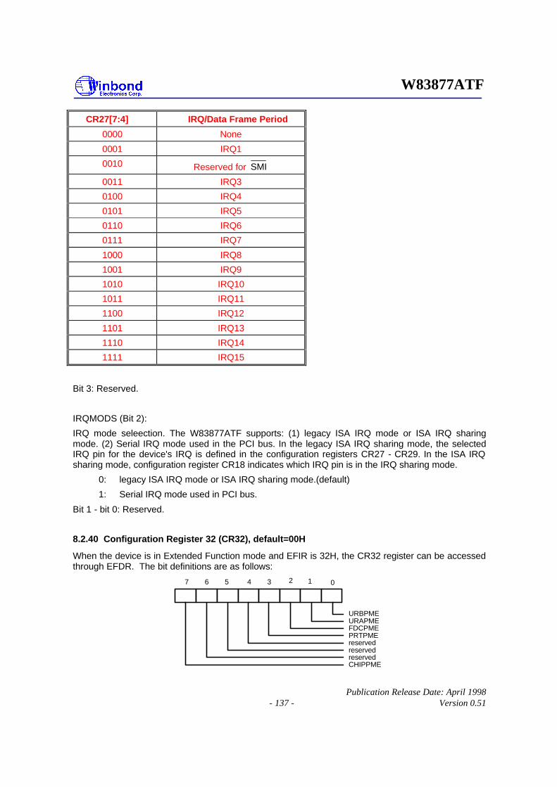
W83877ATF
Publication Release Date: April 1998 - 137 - Version 0.51
CR27[7:4] IRQ/Data Frame Period
0000 None
0001 IRQ1
0010 Reserved for SMI
0011 IRQ3
0100 IRQ4
0101 IRQ5
0110 IRQ6
0111 IRQ7
1000 IRQ8
1001 IRQ9
1010 IRQ10
1011 IRQ11
1100 IRQ12
1101 IRQ13
1110 IRQ14
1111 IRQ15
Bit 3: Reserved.
IRQMODS (Bit 2):
IRQ mode seleection. The W83877ATF supports: (1) legacy ISA IRQ mode or ISA IRQ sharing mode. (2) Serial IRQ mode used in the PCI bus. In the legacy ISA IRQ sharing mode, the selected IRQ pin for the device's IRQ is defined in the configuration registers CR27 - CR29. In the ISA IRQ sharing mode, configuration register CR18 indicates which IRQ pin is in the IRQ sharing mode.
0: legacy ISA IRQ mode or ISA IRQ sharing mode.(default)
1: Serial IRQ mode used in PCI bus.
Bit 1 - bit 0: Reserved.
8.2.40 Configuration Register 32 (CR32), default=00H
When the device is in Extended Function mode and EFIR is 32H, the CR32 register can be accessed through EFDR. The bit definitions are as follows:
1234567 0
URBPMEURAPMEFDCPMEPRTPMEreservedreservedreservedCHIPPME

W83877ATF
Publication Release Date: April 1998 - 138 - Version 0.51
CHIPPME (Bit 7): W83877ATF chip power management enable.
0 disable the ACPI/Legacy and the auto power management functions.
1 enable the ACPI/Legacy and the auto power management functions.
Bit 6 - bit 4: Reserved.
PRTPME (Bit 3): Printer port power management enable.
0 disable the auto power management function.
1 enable the auto power management function, if this bit and CHIPPME(CR32 bit 7) are both set to 1.
FDCPME (Bit 2): FDC power management enable.
0 disable the auto power management function.
1 enable the auto power management function, if this bit and CHIPPME(CR32 bit 7) are both set to 1.
URAPME (Bit 1): UART A power management enable.
0 disable and the auto power management function.
1 enable auto power management function, if this bit and CHIPPME(CR32 bit 7) are both set to 1.
.
URBPME (Bit 0): UART B power management enable.
0 disable the auto power management functions.
1 enable the auto power management function, if this bit and CHIPPME(CR32 bit 7) are both set to 1.

W83877ATF
Publication Release Date: April 1998 - 139 - Version 0.51
8.2.41 Configuration Register 33 (CR33), default=00H
When the device is in Extended Function mode and EFIR is 33H, the CR33 register can be accessed through EFDR. The bit definitions are as follows:
1234567 0
reservedreservedPM1AD2PM1AD3PM1AD4PM1AD5PM1AD6PM1AD7
PM1AD7 - PM1AD2 (Bit 7 - bit 2): Base address of the power management register block PM1.
This address is the base address of PM1a_EVT_BLK in the ACPI specification. The based address should range from 01,0000,0000b to 11,1111,0000b ,i.e., 100H ~ 3F0H, where bit 1 and bit 0 of the base address should be set to 0 and the based address is in the 16-byte alignment. Note that the based address of PM1a_CNT_BLK is equal to PM1a_EVT_BLK + 4, and PM_TMR_BLK is equal to PM1a_EVT_BLK + 8.
Bit 1 - bit 0: Reserved, fixed at 0.
8.2.42 Configuration Register 34 (CR34), default=00H
When the device is in Extended Function mode and EFIR is 34H, the CR34 register can be accessed through EFDR. The bit definitions are as follows:
1234567 0
reservedGPEAD1GPEAD2GPEAD3GPEAD4GPEAD5GPEAD6GPEAD7
GPEAD7 - GPEAD1 (Bit7 - bit 1): Base address of the power management register block GPE.
This address is the base address of GPE0_BLK in the ACPI specification. The base address should range from 01,0000,0000b to 11,1111,1000b ,i.e., 100H ~ 3F8H, where bit 0 of the base address should be set to 0 and the base address is in the 8-byte alignment. Note that the base address of GPE1_BLK is GPE0_BLK + 4.
Bit 0: Reserved, fixed at 0.

W83877ATF
Publication Release Date: April 1998 - 140 - Version 0.51
8.2.43 Configuration Register 35 (CR35), default=00H
When the device is in Extended Function mode and EFIR is 35H, the CR35 register can be accessed through EFDR. The bit definitions are as follows:
1234567 0
URACNT0URACNT1URACNT2URACNT3URACNT4URACNT5URACNT6URACNT7
URACNT7 - URACNT0 (Bit 7 - bit 0): UART A idle timer count.
This register is used to specify the initial value of UART A idle timer. Once UART A enters the working state (that is, after any access to this device, any IRQ, and any external input), the power down machine of UART A reloads this count value and the idle timer counts down. When the timer counts down to zero, UART A enters the power down state ,i.e., sleeping state. If this register is set to 00H, the power down function will be invalid. The time resolution of this value is minute or second, which is defined by the TMIN_SEL bit of the CR3A. Note that (1). This register is valid only when the power management function of UART A is enabled, that is, CHIPPME=1 (CR32 bit 7) and URAPME=1 (CR32 bit 1), (2). If the register is set to 00H, UART A will remain in the current state (working or sleeping).
8.2.44 Configuration Register 36 (CR36), default=00H
When the device is in Extended Function mode and EFIR is 36H, the CR36 register can be accessed through EFDR. The bit definitions are as follows:
1234567 0
URBCNT0URBCNT1URBCNT2URBCNT3URBCNT4URBCNT5URBCNT6URBCNT7
URBCNT7 - URBCNT0 (Bit 7 - bit 0): UART B idle timer count.
This register is used to specify the initial value of UART B idle timer. Once UART B enters the working state (that is, after any access to this device, any IRQ, and any external input), the power down machine of UART B reloads this count value and the idle timer counts down. When the timer counts down to zero, UART B enters the power down state ,i.e., sleeping state. If this register is set to 00H, the power down function will be invalid. The time resolution of this value is minute or second, which is defined by the TMIN_SEL bit of CR3A. Note that (1). This register is valid only when the power management function of UART B is enabled, that is, CHIPPME=1 (CR32 bit 7) and URBPME=1 (CR32 bit 0), (2). If the register is set to 00H, UART B will remain in the current state (working or sleeping).

W83877ATF
Publication Release Date: April 1998 - 141 - Version 0.51
8.2.45 Configuration Register 37 (CR37), default=00H
When the device is in Extended Function mode and EFIR is 37H, the CR37 register can be accessed through EFDR. The bit definitions are as follows:
1234567 0
FDCCNT0FDCCNT1FDCCNT2FDCCNT3FDCCNT4FDCCNT5FDCCNT6FDCCNT7
FDCCNT7 - FDCCNT0 (Bit 7 - bit 0): FDC idle timer count.
This register is used to specify the initial value of FDC idle timer. Once FDC enters the working state (that is, after any access to this device, any IRQ, and any external input), the power down machine of FDC reloads this count value and the idle timer counts down. When the timer counts down to zero, FDC enters the power down state ,i.e., sleeping state. If this register is set to 00H, the power down function will be invalid. The time resolution of this value is minute or second, which is defined by the TMIN_SEL bit of the CR3A. Note that (1). This register is valid only when the power management function of FDC is enabled, that is, CHIPPME=1 (CR32 bit 7) and FDCPME=1 (CR32 bit 2), (2). If the register is set to 00H, FDC will remain in the current state (working or sleeping).
8.2.46 Configuration Register 38 (CR38), default=00H
When the device is in Extended Function mode and EFIR is 38H, the CR38 register can be accessed through EFDR. The bit definitions are as follows:
1234567 0
PRTCNT0PRTCNT1PRTCNT2PRTCNT3PRTCNT4PRTCNT5PRTCNT6PRTCNT7
PRTCNT7 - PRTCNT0 (Bit 7 - bit 0): printer port idle timer count.
This register is used to specify the initial value of the printer port idle timer. Once the printer port enters the working state (that is, after any access to this device, any IRQ, and any external input), the power down machine of the printer port reloads this count value and this idle timer counts down. When the timer counts down to zero, printer port enters the power down state ,i.e., sleeping state. If this register is set to 00H, the power down function will be invalid. The time resolution of this value is minute or second, which is defined by the TMIN_SEL bit of CR3A. Note that (1). This register is valid only when the power management function of the printer port is enabled, that is, CHIPPME=1 (CR32 bit 7) and PRTPME=1 (CR32 bit 3), (2). If the register is set to 00H, the printer port will remain in the current state (working or sleeping).

W83877ATF
Publication Release Date: April 1998 - 142 - Version 0.51
8.2.47 Configuration Register (CR39), default=00H
When the device is in Extended Function mode and EFIR is 39H, the CR39 register can be accessed through EFDR. The bit definitions are as follows:
1234567 0
GSBCNT0GSBCNT1GSBCNT2GSBCNT3GSBCNT4GSBCNT5GSBCNT6GSBCNT7
GSBCNT7 - GSBCNT0 (Bit 7 - bit 0): global stand-by idle timer count.
Once all devices of the chip (including UART A, UART B, FDC and the printer port) are all in the power down state, the power down machine of W83877ATF chip loads this register value and counts down. When the timer counts to zero, the whole chip enters the power down state, i.e., sleeping state. If this register is set to 0, the power down function will be invalid. The time resolution of this register value is minute or second, which is defined by the TMIN_SEL bit of CR3A. Note that (1). This register is valid when the CHIPPME = 1 (CR32 bit 7), and (2) If the register is set to 00H, W83877ATF chip will remain in the current state (working or sleeping).
8.2.48 Configuration Register 3A (CR3A), default=00H
When the device is in Extended Function mode and EFIR is 3AH, the CR3A register can be accessed through EFDR. The bit definitions are as follows:
7 6 5 4 3 2 1 0
UPULLENreservedSMI_ENreservedreservedTMIN_SELreservedreserved
Bit 7 - bit 6 : Reserved, fixed at 0. TMIN_SEL (Bit 5): Time resolution of the auto power machines of all devices.
CR35 to CR39 store the initial counts of the devices.
0 one second
1 one miniute

W83877ATF
Publication Release Date: April 1998 - 143 - Version 0.51
Bit 4 - bit 2: Reserved, fixed at 0. SMI_EN (Bit 2): SMI output pin enable. While an SMI event is raised on the output of the SMI logic, this bit determines whether the SMI
interrupt is generated on the SMI output SMI pin and on the Serial IRQ IRQSER pin while in Serial IRQ mode.
0 disable
1 enable
Bit 1:Reserved. UPULLEN (Bit 0): Enable the pull up of IRQSER pin in Serial IRQ mode.
0 disable the pull up of IRQSER pin.
1 enable the pull up of IRQSER pin.
8.2.49 Configuration Register 3B (CR3B), default=00H Reserved for testing. Should be kept all 0's. 8.2.50 Configuration Register 40 (CR40), default=00H When the device is in Extended Function mode and EFIR is 40H, the CR40 register can be accessed through EFDR. The bit definitions are as follows:
1234567 0
URBIDLSTSURAIDLSTSFDCIDLSTSPRTIDLSTSreservedreservedreservedreserved
Bit 7 - bit 4 : Reserved, fixed at 0. Bit 3 - bit 0 : Devices' idle status. These bits indicate that the individual device's idle timer expires due to no I/O access, IRQ, and external input to the device respectively. These 4 bits are controlled by the printer port, FDC, UART A, and UART B power down machines individually. The bits are set/cleared by W83877ATF automatically. Writing a 1 can also clear this bit, and writing a 0 has no effect.
PRTIDLSTS (Bit 3): printer port idle status.
0 printer port is now in the working state.
1 printer port is now in the sleeping state due to no printer port access, IRQ, DMA acknowledge, and no transition on BUSY, ACK , PE, SLCT, and ERR pins.

W83877ATF
Publication Release Date: April 1998 - 144 - Version 0.51
FDCIDLSTS (Bit 2): FDC idle status.
0 FDC is now in the working state.
1 FDC is now in the sleeping state due to no FDC access, no IRQ, no DMA acknowledge, and no enabling of the motor enable bits in the DOR register.
URAIDLSTS (Bit 1): UART A idle status.
0 UART A is now in the working state.
1 UART A is now in the sleeping state due to no UART A access, no IRQ, the receiver is now waiting for a start bit, the transmitter shift register is now empty, and no transition on MODEM control input lines.
URBIDLSTS (Bit 0): UART B idle status.
0 UART B is now in the working state.
1 UART B is now in the sleeping state due to no UART B access, no IRQ, the receiver is now waiting for a start bit, the transmitter shift register is now empty, and no transition on MODEM control input lines.
8.2.51 Configuration Register 41 (CR41), default=00H
When the device is in Extended Function mode and EFIR is 41H, the CR41 register can be accessed through EFDR. The bit definitions are as follows:
1234567 0
URBTRAPSTSURATRAPSTSFDCTRAPSTSPRTTRAPSTSreservedreservedreservedreserved
Bit 7 - bit 4 : Reserved, fixed at 0.
Bit 3 - bit 0 : Devices' trap status.
These bits indicate that the individual device wakes up due to any I/O access, IRQ, and external input to the device respectively. The device's idle timer reloads the initial count value from CR35-CR39, depending on which device wakes up. These 4 bits are controlled by the printer port, FDC, UART A, and UART B power down machines individually. The bits are set/cleared by W83877ATF automatically. Writing a 1 can also clear this bit, and writing a 0 has no effect.

W83877ATF
Publication Release Date: April 1998 - 145 - Version 0.51
PRTTRAPSTS (Bit 3): printer port trap status.
0 the printer port is now in the sleeping state.
1 the printer port is now in the working state due to any printer port access, any IRQ, any DMA acknowledge, and any transition on BUSY, ACK , PE, SLCT, and ERR pins.
FDCTRAPSTS (Bit 2): FDC trap status.
0 FDC is now in the sleeping state.
1 FDC is now in the working state due to any FDC access, any IRQ, any DMA acknowledge, and any enabling of the motor enable bits in the DOR register.
URATRAPSTS (Bit 1): UART A trap status.
0 UART A is now in the sleeping state.
1 UART A is now in the working state due to any UART A access, any IRQ, the receiver begins receiving a start bit, the transmitter shift register begins transmitting a start bit, and any transition on MODEM control input lines.
URBTRAPSTS (Bit 0): UART B trap status.
0 UART B is now in the sleeping state.
1 UART B is now in the working state due to any UART B access, any IRQ, the receiver begins receiving a start bit, the transmitter shift register begins transmitting a start bit, and any transition on MODEM control input lines.
8.2.52 Configuration Register 42 (CR42), default=N/A
When the device is in Extended Function mode and EFIR is 42H, the CR42 register can be accessed through EFDR. The bit definitions are as follows:
1234567 0
URBIRQSTSURAIRQSTSFDCIRQSTSPRTIRQSTSreservedreservedreservedreserved
Bit 7 - bit 4 : Reserved, fixed at 0.
Bit 3 - bit 0 : Device's IRQ status .

W83877ATF
Publication Release Date: April 1998 - 146 - Version 0.51
These bits indicate the IRQ pin status of the individual device. The device's IRQ status bit is set or cleared at their source device; writing a 1 or 0 has no effect.
PRTIRQSTS (Bit 3) : printer port IRQ status. While the IRQ type of printer port is edge trigger-type, this bit will set and reset immediately. As the software reads this bit, it indicates low level. The software must read the IRQ status bit in the printer port device register to correctly identify whether the printer port IRQ occurs.
FDCIRQSTS (Bit 2) : FDC IRQ status.
URAIRQSTS (Bit 1) : UART A IRQ status.
URBIRQSTS (Bit 0) : UART B IRQ status.
8.2.53 Configuration Register 43 (CR43), default=00H
When the device is in Extended Function mode and EFIR is 43H, the CR43 register can be accessed through EFDR. This register is reserved.
8.2.54 Configuration Register 44 (CR44), default=00H
When the device is in Extended Function mode and EFIR is 44H, the CR44 register can be accessed through EFDR. This register is reserved.
8.2.55 Configuration Register 45 (CR45), default=00H
When the device is in Extended Function mode and EFIR is 45H, the CR45 register can be accessed through EFDR. The bit definitions are as follows:
1234567 0
URBIRQENURAIRQENFDCIRQENPRTIRQENreservedreservedreservedreserved
Bit 7 - bit 4 : Reserved, fixed at 0.
Bit 3 - bit 0 : Enable bits of the SMI generation due to the device's IRQ.

W83877ATF
Publication Release Date: April 1998 - 147 - Version 0.51
These bits enable the generation of an SMI interrupt due to any IRQ of the devices respectively. These 4 bits control the printer port, FDC, UART A, and UART B SMI logics individually. The SMI logic output for the IRQs is as follows:
SMI logic output = (URBIRQEN and URBIRQSTS) or (URAIRQEN and URAIRQSTS) or (FDCIRQEN and FDCIRQSTS) or (PRTIRQEN and PRTIRQSTS)
If any device's IRQ is raised, the coresponding IRQ status bit in CR42 is set. If the device's enable bit is set and SMI_EN(in CR3A) and CHIPPME(in CR32) is both set, then SMI interrupt occurs on the SMI output pin.
PRTIRQEN (Bit 3):
0 disable the generation of an SMI interrput due to the printer port's IRQ.
1 enable the generation of an SMI interrput due to the printer port's IRQ.
FDCIRQEN (Bit 2):
0 disable the generation of an SMI interrupt due to the FDC's IRQ.
1 enable the generation of an SMI interrupt due to the FDC's IRQ.
URAIRQEN (Bit 1):
0 disable the generation of an SMI interrupt due to the UART A's IRQ.
1 enable the generation of an SMI interrupt due to the UART A's IRQ.
URBIRQEN (Bit 0):
0 disable the generation of an SMI interrupt due to the UART B's IRQ.
1 enable the generation of an SMI interrupt due to the UART B's IRQ.

W83877ATF
Publication Release Date: April 1998 - 148 - Version 0.51
8.2.56 Bit Map Configuration Registers Table 8-1: Bit Map of Configuration Registers
Register
Power-on Reset Value
D7
D6
D5
D4
D3
D2
D1
D0
CR0 0000 0000 0 0 0 0 PRTMODS1 PRTMODS0 0 IPD
CR1 0000 0000 ABCHG 0 0 0 0 0 0 0
CR2 0000 0000 0 0 0 0 0 0 0 0
CR3 0011 0000 0 0 EPPVER 0 0 0 SUAMIDI SUBMIDI
CR4 0000 0000 PRTPWD 0 URAPWD URBPWD PRTTRI 0 URATRI URBTRI
CR5 0000 0000 0 0 0 0 ECPFTHR3 ECPFTHR2 ECPFTHR1 ECPFTHR0
CR6 0000 0000 0 0 SEL4FDD FIPURDWN FDCPWD 0 FDCTRI 0
CR7 0000 0000 FDD D T1 FDD D T0 FDD C T1 FDD C T0 FDD B T1 FDD B T0 FDD A T1 FDD A T0
CR8 0000 0000 0 0 DISFDDWR SWWP MEDIA 1 MEDIA 0 BOOT 1 BOOT 0
CR9 0000 1101 PRTMODS2 LOCKREG EN3MODE 0 CHIP ID 3 CHIP ID 2 CHIP ID 1 CHIP ID 0
CRA 0000 0000 0 0 0 0 0 0 0 0
CRB 0000 1100 0 Tx4WC Rx4WC ENIFCHG IDENT MFM INVERTZ DRV2EN
CRC 0010 1000 TURA TURB HEFERE 0 URIRSEL 0 RX2INV TX2INV
CRD 1010 0011 SIRTX1 SIRTX0 SIRRX1 SIRRX0 HDUPLX IRMODE2 IRMODE1 IRMODE0
CR10 0000 0000 GIO0AD7 GIO0AD6 GIO0AD5 GIO0AD4 GIO0AD3 GIO0AD2 GIO0AD1 GIO0AD0
CR11 0000 0000 G0CADM1 G0CADM0 0 0 0 GIO0AD10 GIO0AD9 GIO0AD8
CR12 0000 0000 GIO1AD7 GIO1AD6 GIO1AD5 GIO1AD4 GIO1AD3 GIO1AD2 GIO1AD1 GIO1AD0
CR13 0000 0000 G1CADM1 G1CADM0 0 0 0 GIO1AD10 GIO1AD9 GIO1AD8
CR14 0000 0000 GIOP0MD2 GIOP0MD1 GIOP0MD0 GIO0CSH GCS0IOR GCS0IOW GDA0OPI GDA0IPI
CR15 0000 0000 GIOP1MD2 GIOP1MD1 GIOP1MD0 GIO1CSH GCS1IOR GCS1IOW GDA1OPI GDA1IPI
CR16 00ss 0s0s1 0 0 G1IQSEL G0IQSEL 0 PNPCVS 0 HEFRAS
CR17 0000 0000 0 0 0 PRIRQOD DSFDLGRQ DSPRLGRQ DSUALGRQ DSUBLGRQ
CR18 0000 0000 SHARH SHARG SHARF SHARE SHARD SHARC SHARB SHARA
CR19 0000 0000 0 0 0 0 0 0 FASTA FASTB

W83877ATF
Publication Release Date: April 1998 - 149 - Version 0.51
ContinuedTable 8-1: Bit Map of Configuration Registers
CR20 1111 11002 FDCAD7 FDCAD6 FDCAD5 FDCAD4 FDCAD3 FDCAD2 0 0
CR23 1101 11102 PRTAD7 PRTAD6 PRTAD5 PRTAD4 PRTAD3 PRTAD2 PRTAD1 PRTAD0
CR24 1111 11102 URAAD7 URAAD6 URAAD5 URAAD4 URAAD3 URAAD2 URAAD1 0
CR25 1011 11102 URBAD7 URBAD6 URBAD5 URBAD4 URBAD3 URBAD2 URBAD1 0
CR26 0010 00112 FDCDQS3 FDCDQS2 FDCDQS1 FDCDQS0 PRTDQS3 PRTDQS2 PRTDQS1 PRTDQS0
CR27 0000 01012 ECPIRQx2 ECPIRQx1 ECPIRQx0 0 PRTIQS3 PRTIQS2 PRTIQS1 PRTIQS0
CR28 0100 00112 URAIQS3 URAIQS2 URAIQS1 URAIQS0 URBIQS3 URBIQS2 URBIQS1 URBIQS0
CR29 0110 00002 FDCIQS3 FDCIQS2 FDCIQS1 FDCIQS0 IQNIQS3 IQNIQS2 IQNIQS1 IQNIQS0
CR2A 0000 0000 IRTXDSL3 IRTXDSL2 IRTXDSL1 IRTXDSL0 IRRXDSL3 IRRXDSL2 IRRXDSL1 IRRXDSL0
CR2B 0000 0000 PIN1FUN1 PIN1FUN0 PIN2FUN1 PIN2FUN0 PIN3FUN1 PIN3FUN0 PIN93FUN1 PIN93FUN0
CR2C 0000 0000 PIN91FUN2 PIN91FUN1 PIN91FUN0 APEDCRC ENBNKSL CLKINSEL 0 0
CR2D 0000 0000 0 0 DIS-PRECOM1 DRTB 1 DRTB 0 DIS-PRECOM0 DRTA 1 DRTA 0
CR31 0000 0s00 SCIIRQ3 SCIIRQ2 SCIIRQ1 SCIIRQ0 0 IRQMODS 0 0
CR32 0000 0000 CHIPPME 0 0 0 PRTPME FDCPME URAPME URBPME
CR33 0000 0000 PM1AD7 PM1AD6 PM1AD5 PM1AD4 PM1AD3 PM1AD2 0 0
CR34 0000 0000 GPEAD7 GPEAD6 GPEAD5 GPEAD4 GPEAD3 GPEAD2 GPEAD1 0
CR35 0000 0000 URACNT7 URACNT6 URACNT5 URACNT4 URACNT3 URACNT2 URACNT1 URACNT0
CR36 0000 0000 URBCNT7 URBCNT6 URBCNT5 URBCNT4 URBCNT3 URBCNT2 URBCNT1 URBCNT0
CR37 0000 0000 FDCCNT7 FDCCNT6 FDCCNT5 FDCCNT4 FDCCNT3 FDCCNT2 FDCCNT1 FDCCNT0
CR38 0000 0000 PRTCNT7 PRTCNT6 PRTCNT5 PRTCNT4 PRTCNT3 PRTCNT2 PRTCNT1 PRTCNT0
CR39 0000 0000 GSBCNT7 GSBCNT6 GSBCNT5 GSBCNT4 GSBCNT3 GSBCNT2 GSBCNT1 GSBCNT0
CR3A 0000 0000 0 0 TMIN_SEL 0 0 SMI_EN 0 UPULLEN
CR40 0000 0000 0 0 0 0 PRTIDLSTS FDCIDLSTS URAIDLSTS URBIDLSTS
CR41 0000 0000 0 0 0 0 PRTTRAPSTS FDCTRAPSTS URATRAPSTS URBTRAPSTS
CR42 0000 0000 0 0 0 0 PRTIRQSTS FDCIRQSTS URAIRQSTS URBIRQSTS
CR43 0000 0000 0 0 0 0 0 0 0 0
CR44 0000 0000 0 0 0 0 0 0 0 0
CR45 0000 0000 0 0 0 0 PRTIRQEN FDCIRQEN URAIRQEN URBIRQEN
Notes: 1. 's' means its value depends on corresponding power-on setting pin. 2. These default values are valid when CR16 bit 2 is 1 during power-on reset; They will be all 0's if CR16 bit 2 is 0.

W83877ATF
Publication Release Date: April 1998 - 150 - Version 0.51
8.3 ACPI Registers Features
W83877ATF supports both the ACPI and legacy power managements. The switch logic of the power managment block generates an SMI interrupt in the legacy mode and an SCI interrupt in the ACPI mode. For the legacy mode, the SMI_EN bit is used. If it is set, it routes the power management events from the SMI interrupt logic to the SMI output pin. For the ACPI mode, the SCI_EN bit is used. If it is set, it routes the power management events to the SCI interrupt logic. The SMI_EN bit is located in the CR3A register and the SCI_EN bit is located in the PM1 register block. See the following figure for an illustration.
PM Timer
Device IdleTimers
Device Trap
Timer
SMI Logic
SMI_EN
SMI outputLogic
SCI outputLogic
Sleep/WakeState machine
WAK_STS
ClockControl
SCI
SMI
SCI Logic
Global STBY
SCI events
0
1
SCI_EN
SMI events
IRQs
IRQs
IRQs
The SMI interrupt is routed to pin SMI , which is dedicated for the SMI interrupt output. Another way to output the SMI interrupt is to route to pin IRQSER, which is the signal pin in the Serial IRQ mode. The SCI interrupt is routed to pin SCI , which is dedicated for the SCI function. The other way to output the SCI interrupt is to route to one interrupt request signal pin IRQA~H, which is selected through CR31 bit[7:4]. Another way is output the SCI interrupt is to route to pin IRQSER.

W83877ATF
Publication Release Date: April 1998 - 151 - Version 0.51
8.3.1 SMI to SCI/SCI to SMI and Bus Master
For the process of generating an interrupt from SMI to SCI or from SCI to SMI, see the following figure for an illustration.
BIOS_RLS
GBL_EN
from SCI to SMI
GBL_RLS
BIOS_EN
Bus Master SCI
BM_CNTPL
BM_RLD
clear
set
BM_STS
To SCI Logic
To SMI Logic
To SCI Logic
from SMI to SCI
clear
set
clear
set
GBL_STS
BIOS_STS
: Status bit
: Enable bit
For the BIOS software to raise an event to the ACPI software, BIOS_RLS, GBL_EN, and GBL_STS bits are involved. GBL_EN is the enable bit and the GBL_STS is the status bit. Both are controlled by the ACPI software. If BIOS_RLS is set by the BIOS software and GBL_EN is set by the ACPI software, an SCI interrupt is raised. Writing a 1 to BIOS_RLS sets it to logic 1 and also sets GBL_STS to logic 1; Writing a 0 to BIOS_RLS has no effect. Writing a 1 to GBL_STS clears it to logic 0 and also clears BIOS_RLS to logic 0; writing a 0 to GBL_STS has no effect.
For the ACPI software to raise an event to the BIOS software, GBL_RLS, BIOS_EN, and BIOS_STS bits are involved. BIOS_EN is the enable bit and the BIOS_STS is the status bit. Both are controlled by the BIOS software. If GBL_RLS is set by the ACPI software and BIOS_EN is set by the BIOS software, an SMI is raised. Writing a 1 to GBL_RLS sets it to logic 1 and also sets BIOS_STS to logic 1; Writing a 0 to GBL_RLS has no effect. Writing a 1 to BIOS_STS clears it to logic 0 and also clears GBL_RLS to logic 0; writing a 0 to BIOS_STS has no effect.
For the bus master to raise an event to the ACPI software, BM_CNTRL, BM_RLD, and BM_STS bits are involved. Both BM_RLD and BM_STS are controlled by the ACPI software. If BM_CNTRL is set

W83877ATF
Publication Release Date: April 1998 - 152 - Version 0.51
by the BIOS software and BM_RLD is set by the ACPI software, an SCI interrupt is raised. Writing a 1 to BM_CNTRL sets it to logic 1 and also sets BM_STS to logic 1; Writing a 0 to BM_CNTRL has no effect. Writing a 1 to BM_STS clears it to logic 0 and also clears BM_CNTRL to logic 0; writing a 0 to BM_STS has no effect.
8.3.2 Power Management Timer
In the ACPI specification, a power management timer is required. The power management timer is a 24-bit fixed rate free running count-up timer that runs off a 3.579545MHZ clock. The power management timer has the corresponding status bit (TMR_STS) and enable bit (TMR_EN). The TMR_STS bit is set any time the last bit of the timer (bit 23) goes from 0 to 1 or from 1 to 0. If the TMR_EN bit is set, the setting of the TMR_STS bit will generate an SCI interrupt. Three registers are used to read the timer value; they are located in the PM1 register block. The power management timer has one enable bit (TMR_ON) to turn if on or off. The TMR_ON is located in GPE register block. If it is cleared to 0, the power management timer function will not work. There are no timer reset requirements, except that the timer should function after power-up. See the following figure for an illustration.
To SCI Logic
24 bitcounter
Bits (23-0)
TMR_STS
TMR_EN
TMR_ON
3.579545 MHz
24
TMR_VAL
8.4 ACPI Registers (ACPIRs)
The ACPI register model consists of the fixed register blocks that perform the ACPI functuions. A register block may be a event register block which deals with ACPI events, or a control register block which deals with control features. The ordering in the event register block is the status register, followed by the enable register.
Each event register, if implemented, contains two egisters: a status register and an enable register, both in 16-bit size. The status register indicates what defined function needs the ACPI System Control Interrupt (SCI). When the hardware event occurs, the defined status bit is set. However, to generate the SCI, the associated enable bit must be set. If the enable bit is not set, the software can examine the state of the hardware event by reading the status bit without generating an SCI interrupt.
Any status bit, unless otherwise noted, can only be set by some defined hardware event. It is cleared by writing a 1 to its bit position; writing a 0 has no effect. Except forsome special status bits, every status bit has an assiciated enable bit in the same bit position in the enable register. Those status bits which have no respective enable bit are read for special purposes. Reserved or un-implemented enable bits always return zero, and writing to these bits should have no effect.

W83877ATF
Publication Release Date: April 1998 - 153 - Version 0.51
The control bit in the control register provides some special control functions over the hardware event, or some special control over SCI event. Reserved or un-implemented control bits always return zero, and writing to those bits should have no effect.
Table 8-4 lists the PM1 register block and the relative locations of the registers within it. The base address of PM1 register block is named as PM1a_EVT_BLK in the ACPI specification. The base address should range from 01,0000,0000b to 11,1111,0000b ,i.e., 100H ~ 3F0H, where bit 1 and bit 0 of PM1 register block should be set to 0 and the base address is in the 16-byte alignment.
Table 8-5 lists the GPE register block and the relative locations within it. The base address of power management event block GPE is named as GPE0_BLK in the ACPI specification. The base address should range from 01,0000,0000b to 11,1111,1000b ,i.e., 100H ~ 3F8H, where bit 0 of the base address should be set to 0 and the base address is in the 8-byte alignment.
8.4.1 Power Management 1 Status Register 1 (PM1STS1)
Register Location: <CR33> System I/O Space
Default Value: 00h
Attribute: Read/write
Size: 8 bits
1234567 0
TMR_STSReservedReservedReservedBM_STSGBL_STSReservedReserved
Bit Name Description
0 TMR_STS This bit is the timer carry status bit. This bit gets set anytime the bit 23 of the 24-bit counter changes (whenever the MSB changes from low to high or high to low). While TMR_EN and TMR_STS are set, a power magement event is raised. This bit is only set by hardware and can only be cleared by the software writing a 1 to this bit position. Writing a 0 has no effect.
1-3 Reserved Reserved.
4 BM_STS This is the bus master status bit. Writing a 1 to BM_CNTRL also sets BM_STS. Writing a 1 clears this bit and also clears BM_CNTRL. Writing a 0 has no effect.
5 GBL_STS This is the global status bit. This bit is set when the BIOS want the attention of the SCI handler. BIOS sets this bit by setting BIOS_RLS and can only be cleared by software writing a 1 to this bit position. Writing a 1 to this bit position also clears BIOS_RLS. Writing a 0 has no effect.
6-7 Reserved Reserved. These bits always return a value of zero.

W83877ATF
Publication Release Date: April 1998 - 154 - Version 0.51
8.4.2 Power Management 1 Status Register 2 (PM1STS2)
Register Location: <CR33>+1H System I/O Space
Default Value: 00h
Attribute: Read/write
Size: 8 bits
1234567 0
ReservedReservedReservedReservedReservedReservedReservedWAK_STS
Bit Name Description
0-6 Reserved Reserved.
7 WAK_STS This bit is set when the system is in the sleeping state and an enabled resume event occurs. Upon setting this bit, the sleeping/working state machine will transition the system to the working state. This bit is only set by hardware, and is cleared by software writing a 1 to this bit position or by the sleeping/working state machine automatically upon the expiry of the global standby timer. Writing a 0 has no effect. Upon the WAK_STS beingcleared and all devices being in sleeping state, the whole chip enters the sleeping state.
8.4.3 Power Management 1 Enable Register 1(PM1EN1)
Register Location: <CR33>+2H System I/O Space
Default Value: 00h
Attribute: Read/write
Size: 8 bits
1234567 0
TMR_ENReservedReservedReservedGBL_ENReservedReservedReserved

W83877ATF
Publication Release Date: April 1998 - 155 - Version 0.51
Bit Name Description
0 TMR_EN This is the timer carry interrupt enable bit. When this bit is set, an SCI event is generated anytime the TMR_STS bit is set. When this bit is reset no interrupt is generated when the TMR_STS bit is set.
1-4 Reserved Reserved. These bits always return a value of zero.
5 GBL_EN The global enable bit. When both the GBL_EN bit and the GBL_STS bit are set, an SCI interrupt is raised.
6-7 Reserved Reserved.
8.4.4 Power Management 1 Enable Register 2 (PM1EN2)
Register Location: <CR33>+3H System I/O Space
Default Value: 00h
Attribute: Read/write
Size: 8 bits
1234567 0
ReservedReservedReservedReservedReservedReservedReservedReserved
Bit Name Description
0-7 Reserved Reserved. These bits always return a value of zero.
8.4.5 Power Management 1 Control Register 1 (PM1CTL1)
Register Location: <CR33>+4H System I/O Space
Default Value: 00h
Attribute: Read/write
Size: 8 bits

W83877ATF
Publication Release Date: April 1998 - 156 - Version 0.51
1234567 0
SCI_ENBM_RLDGBL_RLDReservedReservedReservedReservedReserved
Bit Name Description
0 SCI_EN Select the power management event to be either an SCI or an SMI interrupt. When this bit is set, the power management events will generate an SCI interrupt. When this bit is reset and SMI_EN bit is set, the power management events will generate an SMI interrupt.
1 BM_RLD This is the bus master reload enable bit. If this bit is set and BM_CNTRL is set, an SCI interrupt is raised.
2 GBL_RLS The global release bit. This bit is used by the ACPI software to raise an event to the BIOS software. The BIOS software has a corresponding enable and status bit to control its ability to receive the ACPI event. Setting GBL_RLS sets BIOS_STS, and it generates an SMI interrupt if BIOS_EN is also set.
3-7 Reserved Reserved. These bits always return a value of zero.
8.4.6 Power Management 1 Control Register 2 (PM1CTL2)
Register Location: <CR33>+5H System I/O Space
Default Value: 00h
Attribute: Read/write
Size: 8 bits
1234567 0
ReservedReservedReservedReservedReservedReservedReservedReserved
Bit Name Description
0-7 Reserved Reserved. These bits always return a value of zero.

W83877ATF
Publication Release Date: April 1998 - 157 - Version 0.51
8.4.7 Power Management 1 Control Register 3 (PM1CTL3)
Register Location: <CR33>+6H System I/O Space
Default Value: 00h
Attribute: Read/write
Size: 8 bits
1234567 0
ReservedReservedReservedReservedReservedReservedReservedReserved
Bit Name Description
0-7 Reserved Reserved. These bits always return a value of zero.
8.4.8 Power Management 1 Control Register 4 (PM1CTL4)
Register Location: <CR33>+7H System I/O Space
Default Value: 00h
Attribute: Read/write
Size: 8 bits
1234567 0
ReservedReservedReservedReservedReservedReservedReservedReserved
Bit Name Description
0-7 Reserved Reserved. These bits always return a value of zero.

W83877ATF
Publication Release Date: April 1998 - 158 - Version 0.51
8.4.9 Power Management 1 Timer 1 (PM1TMR1)
Register Location: <CR33>+8H System I/O Space
Default Value: 00h
Attribute: Read only
Size: 8 bits
1234567 0
TMR_VAL0TMR_VAL1TMR_VAL2TMR_VAL3TMR_VAL4TMR_VAL5TMR_VAL6TMR_VAL7
Bit Name Description
0-7 TMR_VAL This read-only field returns the running count of the power management timer. This is a 24-bit counter that runs off of a 3.579545 MHZ clock, and counts while in the system working state. The timer is reset and then continues counting until the CLKIN input to the chip is stopped. If the clock is restarted without a MR reset, then the counter will continue counting from where it stopped. The TMR_STS bit is set any time the last bit of the timer (bit 23) goes from 0 to 1 or from 1 to 0. If the TMR_EN bit is set, the setting of the TMR_STS bit will generate an SCI interrupt.
8.4.10 Power Management 1 Timer 2 (PM1TMR2)
Register Location: <CR33>+9H System I/O Space
Default Value: 00h
Attribute: Read only
Size: 8 bits
1234567 0
TMR_VAL8TMR_VAL9TMR_VAL10TMR_VAL11TMR_VAL12TMR_VAL13TMR_VAL14TMR_VAL15

W83877ATF
Publication Release Date: April 1998 - 159 - Version 0.51
Bit Name Description
0-7 TMR_VAL This read-only field returns the running count of the power management timer. This is a 24-bit counter that runs off of a 3.579545 MHZ clock, and counts while in the system working state. The timer is reset and then continues counting until the CLKIN input to the chip is stopped. If the clock is restarted without a MR reset, then the counter will continue counting from where it stopped. The TMR_STS bit is set any time the last bit of the timer (bit 23) goes from 0 to 1 or from 1 to 0. If the TMR_EN bit is set, the setting of the TMR_STS bit will generate an SCI interrupt.
8.4.11 Power Management 1 Timer 3 (PM1TMR3)
Register Location: <CR33>+AH System I/O Space
Default Value: 00h
Attribute: Read only
Size: 8 bits
1234567 0
TMR_VAL16TMR_VAL17TMR_VAL18TMR_VAL19TMR_VAL20TMR_VAL21TMR_VAL22TMR_VAL23
Bit Name Description
0-7 TMR_VAL This read-only field returns the running count of the power management timer. This is a 24-bit counter that runs off of a 3.579545 MHZ clock, and counts while in the system working state. The timer is reset and then continues counting until the CLKIN input to the chip is stopped. If the clock is restarted without a MR reset, then the counter will continue counting from where it stopped. The TMR_STS bit is set any time the last bit of the timer (bit 23) goes from 0 to 1 or from 1 to 0. If the TMR_EN bit is set, the setting of the TMR_STS bit will generate an SCI interrupt.

W83877ATF
Publication Release Date: April 1998 - 160 - Version 0.51
8.4.12 Power Management 1 Timer 4 (PM1TMR4)
Register Location: <CR33>+BH System I/O Space
Default Value: 00h
Attribute: Read only
Size: 8 bits 1234567 0
ReservedReservedReservedReservedReservedReservedReservedReserved
Bit Name Description
0-7 Reserved Reserved. These bits always return a value of zero.
8.4.13 General Purpose Event 0 Status Register 1 (GP0STS1)
Register Location: <CR34> System I/O Space
Default Value: 00h
Attribute: Read/write
Size: 8 bits 1234567 0
URBSCISTSURASCISTSFDCSCISTSPRTSCISTSReservedReservedReservedReserved
These bits indicate the status of the SCI input, which is set when the device's IRQ is raised. If the corresponding enable bit in the SCI interrupt enable register (in GP0EN1) is set, an SCI interrupt is raised and routed to the output pin. Wrinting a 1 clears the bit, and writing a 0 has no effect. If the bit is not cleared, new IRQ for the SCI logic input is ignored, therefore no SCI interrupt is raised.
Bit Name Description
0 URBSCISTS UART B SCI status, which is set by the UART B IRQ.
1 URASCISTS UART A SCI status, which is set by the UART A IRQ.
2 FDCSCISTS FDC SCI status, which is set by the FDC IRQ.
3 PRTSCISTS PRT SCI status, which is set by the printer port IRQ.
4-7 Reserved Reserved.

W83877ATF
Publication Release Date: April 1998 - 161 - Version 0.51
8.4.14 General Purpose Event 0 Status Register 2 (GP0STS2)
Register Location: <CR34>+1H System I/O Space
Default Value: 00h
Attribute: Read/write
Size: 8 bits
1234567 0
ReservedReservedReservedReservedReservedReservedReservedReserved
Bit Name Description
0-7 Reserved Reserved. These bits always return a value of zero.
8.4.15 General Purpose Event 0 Enable Register 1 (GP0EN1)
Register Location: <CR34> +2H System I/O Space
Default Value: 00h
Attribute: Read/write
Size: 8 bits
1234567 0
URBSCIENURASCIENFDCSCIENPRTSCIENReservedReservedReservedReserved
These bits are used to enable the device's IRQ sources onto the SCI logic. The SCI logic output for the IRQs is as follows:
SCI logic output = (URBSCIEN and URBSCISTS) or (URASCIEN and URASCISTS) or (FDCSCIEN and FDCSCISTS) or (PRTSCIEN and PRTSCISTS)

W83877ATF
Publication Release Date: April 1998 - 162 - Version 0.51
Bit Name Description
0 URBSCIEN UART B SCI enable, which controls the UART B IRQ for SCI.
1 URASCIEN UART A SCI enable, which controls the UART A IRQ for SCI.
2 FDCSCIEN FDC SCI enable, which controls the FDC IRQ for SCI.
3 PRTSCIEN Printer port SCI enable, which controls the printer port IRQ for SCI.
4-7 Reserved Reserved.
8.4.16 General Purpose Event 0 Enable Register 2 (GP0EN2)
Register Location: <CR34>+3H System I/O Space
Default Value: 00h
Attribute: Read/write
Size: 8 bits
1234567 0
ReservedReservedReservedReservedReservedReservedReservedReserved
Bit Name Description
0-7 Reserved Reserved. These bits always return a value of zero.
8.4.17 General Purpose Event 1 Status Register 1 (GP1STS1)
Register Location: <CR34>+4H System I/O Space
Default Value: 00h
Attribute: Read/write
Size: 8 bits
1234567 0
BIOS_STSReservedReservedReservedReservedReservedReservedReserved

W83877ATF
Publication Release Date: April 1998 - 163 - Version 0.51
Bit Name Description
0 BIOS_STS The BIOS status bit. This bit is set when GBL_RLS is set. If BIOS_EN is set, setting GBL_RLS will raise an SMI event. Writing a 1 to its bit location clears BIOS_STS and also clears GBL_RLS. Writing a 0 has no effect.
1-7 Reserved Reserved.
8.4.18 General Purpose Event 1 Status Register 2 (GP1STS2)
Register Location: <CR34>+5H System I/O Space Default Value: 00h Attribute: Read/write Size: 8 bits
1234567 0
ReservedReservedReservedReservedReservedReservedReservedReserved
Bit Name Description
0-7 Reserved Reserved. These bits always return a value of zero.
8.4.19 General Purpose Event 1 Enable Register 1 (GP1EN1)
Register Location: <CR34>+6H System I/O Space Default Value: 00h Attribute: Read/write Size: 8 bits
1234567 0
BIOS_ENTMR_ONReservedReservedReservedReservedReservedReserved

W83877ATF
Publication Release Date: April 1998 - 164 - Version 0.51
Bit Name Description
0 BIOS_EN This bit raise the SMI event. When this bit is set and the ACPI software writes a 1 to the GBL_RLS bit, an SMI event is raised on the SMI logic output.
1 TMR_ON This bit is used to turn on the power management timer. 1: timer on ; 0: timer off.
2-7 Reserved Reserved.
8.4.20 General Purpose Event 1 Enable Register 2 (GP1EN2)
Register Location: <CR34>+7H System I/O Space
Default Value: 00h
Attribute: Read/write
Size: 8 bits
1234567 0
BIOS_RLSBM_CNTRLReservedReservedReservedReservedReservedReserved
Bit Name Description
0 BIOS_RLS The BIOS release bit. This bit is used by the BIOS software to raise an event to the ACPI software. The ACPI software has a corresponding enable and status bit to control its ability to receive the ACPI event. Setting BIOS_RLS sets GBL_STS, and it generates an SCI interrupt if GBL_EN is also set. Writing a 1 to its bit position sets this bit and also sets the BM_STS bit. Writing a 0 has no effect. This bit is cleared by writing a 1 to the GBL_STS bit.
1 BM_CNTRL This bit is used to set the BM_STS bit and if the BM_RLD bit is also set, then an SCI interrupt is generated. Writing a 1 sets BM_CNTRL to 1 and also sets BM_STS. Writing a 0 has no effect. Writing a 1 to BM_STS clears BM_STS and also clears BM_CNTRL.
2-7 Reserved Reserved.

W83877ATF
Publication Release Date: April 1998 - 165 - Version 0.51
8.4.21 Bit Map Configuration Registers
Table 8-4: Bit Map of PM1 Register Block Register Address Power-On
Reset Value
D7 D6 D5 D4 D3 D2 D1 D0
PM1STS1 <CR33> 0000 0000 0 0 GBL_STS BM_STS 0 0 0 TMR_STS
PM1STS2 <CR33>+1H 0000 0000 WAK_STS 0 0 0 0 0 0 0
PM1EN1 <CR33>+2H 0000 0000 0 0 GBL_EN 0 0 0 0 TMR_EN
PM1EN2 <CR33>+3H 0000 0000 0 0 0 0 0 0 0 0
PM1CTL1 <CR33>+4H 0000 0000 0 0 0 0 0 GBL_RLS BM_RLD SCI_EN
PM1CTL2 <CR33>+5H 0000 0000 0 0 0 0 0 0 0 0
PM1CTL3 <CR33>+6H 0000 0000 0 0 0 0 0 0 0 0
PM1CTL4 <CR33>+7H 0000 0000 0 0 0 0 0 0 0 0
PM1TMR1 <CR33>+8H 0000 0000 TMR_VAL7 TMR_VAL6 TMR_VAL5 TMR_VAL4 TMR_VAL3 TMR_VAL2 TMR_VAL1 TMR_VAL0
PM1TMR2 <CR33>+9H 0000 0000 TMR_VAL15 TMR_VAL14 TMR_VAL13 TMR_VAL12 TMR_VAL11 TMR_VAL10 TMR_VAL9 TMR_VAL8
PM1TMR3 <CR33>+AH 0000 0000 TMR_VAL23 TMR_VAL22 TMR_VAL21 TMR_VAL20 TMR_VAL19 TMR_VAL18 TMR_VAL17 TMR_VAL16
PM1TMR4 <CR33>+BH 0000 0000 0 0 0 0 0 0 0
Table 8-5: Bit Map of GPE Register Block Register Address Power-On
Reset Value
D7 D6 D5 D4 D3 D2 D1 D0
GP0STS1 <CR34> 0000 0000 0 0 0 0 PRTSCISTS FDCSCISTS URASCISTS URBSCISTS
GP0STS2 <CR34>+1H 0000 0000 0 0 0 0 0 0 0 0
GP0EN1 <CR34>+2H 0000 0000 0 0 0 0 PRTSCIEN FDCSCIEN URASCIEN URBSCIEN
GP0EN2 <CR34>+3H 0000 0000 0 0 0 0 0 0 0 0
GP1STS1 <CR34>+4H 0000 0000 0 0 0 0 0 0 0 BIOS_STS
GP1STS2 <CR34>+5H 0000 0000 0 0 0 0 0 0 0 0
GP1EN1 <CR34>+6H 0000 0000 0 0 0 0 0 0 TMR_ON BIOS_EN
GP1EN2 <CR34>+7H 0000 0000 0 0 0 0 0 0 BM_CNTRL BIOS_RLS

W83877ATF
Publication Release Date: April 1998 - 166 - Version 0.51
9.0 SPECIFICATIONS
9.1 Absolute Maximum Ratings
PARAMETER RATING UNIT
Power Supply Voltage -0.5 to 7.0 V
Input Voltage -0.5 to VDD+0.5 V
Operating Temperature 0 to +70 ° C
Storage Temperature -55 to +150 ° C
Note: Exposure to conditions beyond those listed under Absolute Maximum Ratings may adversely affect the life and reliability of the device.
9.2 DC CHARACTERISTICS
(Ta = 0° C to 70° C, VDD = 5V ± 10%, VSS = 0V)
PARAMETER SYM. MIN. TYP. MAX. UNI CONDITIONS
I/O8tc - TTL level output pin with source-sink capabilities of 8 mA; CMOS level input voltage
Input Low Voltage VIL -0.5 0.3xVDD V
Input High Voltage VIH 0.7xVDD VDD+0.5 V
Output Low Voltage VOL 0.4 V IOL = 8 mA
Output High Voltage VOH 2.4 V IOH = -8 mA
Input High Leakage ILIH +10 µA VIN = VDD
Input Low Leakage ILIL -10 µA VIN = 0V
I/O12t - TTL level bi-directional pin with source-sink capabilities of 12 mA
Input Low Voltage VIL -0.5 0.8 V
Input High Voltage VIH 2.0 VDD+0.5 V
Output Low Voltage VOL 0.4 V IOL = 12 mA
Output High Voltage VOH 2.4 V IOH = -12 mA
Input High Leakage ILIH +10 µA VIN = VDD
Input Low Leakage ILIL -10 µA VIN = 0V
I/O24t - TTL level bi-directional pin with source-sink capabilities of 24 mA
Input Low Voltage VIL -0.5 0.8 V
Input High Voltage VIH 2.0 VDD+0.5 V
Output Low Voltage VOL 0.4 V IOL = 24 mA
Output High Voltage VOH 2.4 V IOH = -24 mA
Input High Leakage ILIH +10 µA VIN = VDD
Input Low Leakage ILIL -10 µA VIN = 0V

W83877ATF
Publication Release Date: April 1998 - 167 - Version 0.51
9.2 DC Characteristics, continued
PARAMETER SYM. MIN. TYP. MAX. UNIT CONDITIONS OUT8t - TTL level output pin with source-sink capabilities of 8 mA
Output Low Voltage VOL 0.4 V IOL = 8 mA
Output High Voltage VOH 2.4 V IOH = -8 mA
OUT12t - TTL level output pin with source-sink capabilities of 12 mA
Output Low Voltage VOL 0.4 V IOL = 12 mA
Output High Voltage VOH 2.4 V IOH = -12 mA
OD12 - Open-drain output pin with sink capabilities of 12 mA
Output Low Voltage VOL 0.4 V IOL = 12 mA
OD24 - Open-drain output pin with sink capabilities of 24 mA
Output Low Voltage VOL 0.4 V IOL = 24 mA
INt - TTL level input pin
Input Low Voltage VIL 0.8 V VDD = 5 V
Input High Voltage VIH 2.0 V VDD = 5 V
Input High Leakage ILIH +10 µA VIN = VDD
Input Low Leakage ILIL -10 µA VIN = 0V
INts - TTL level input pin Schmitt-trigger input pin
Input Low Threshold Voltage Vt- 0.5 0.8 1.1 V VDD = 5 V
Input High Threshold Voltage Vt+ 1.6 2.0 2.4 V VDD = 5 V
Hysteresis (Vt+ - Vt-) VTH 0.5 1.2 V VDD = 5 V
Input High Leakage ILIH +10 µA VIN = VDD
Input Low Leakage ILIL -10 µA VIN = 0V
INc - CMOS level input pin
Input Low Voltage VIL 0.3xVDD V VDD = 5 V
Input High Voltage VIH 0.7xVDD V VDD = 5 V
Input High Leakage ILIH +10 µA VIN = VDD
Input Low Leakage ILIL -10 µA VIN = 0V
INcs - CMOS level schmitt-triggered input pin
Input Low Threshold Voltage Vt- 1.3 1.5 1.7 V VDD = 5 V
Input High Threshold Voltage Vt+ 3..2 3.5 3.8 V VDD = 5 V
Hysteresis (Vt+ - Vt-) VTH 1.5 2 V VDD = 5 V
Input High Leakage ILIH +10 µA VIN = VDD
Input Low Leakage ILIL -10 µA VIN = 0V

W83877ATF
Publication Release Date: April 1998 - 168 - Version 0.51
9.3 AC Characteristics
FDC: Data rate = 1 MB/500 KB/300 KB/250 KB/sec.
PARAMETER SYM. TEST CONDITIONS
MIN. TYP. (NOTE 1)
MAX. UNIT
SA9-SA0, AEN, DACK , CS, setup time to IOR¡õ
TAR 25 nS
SA9-SA0, AEN, DACK , hold time for IOR¡ô
TAR 0 nS
IOR width TRR 80 nS
Data access time from IOR¡õ
TFD CL = 100 pf 80 nS
Data hold from IOR¡õ TDH CL = 100 pf 10 nS
SD to from IOR ¡ô TDF CL = 100 pf 10 50 nS
IRQ delay from IOR ¡ô TRI 360/570 /675
nS
SA9-SA0, AEN, DACK , setup time to IOW ¡õ
TAW 25 nS
SA9-SA0, AEN, DACK , hold time for IOW ¡ô
TWA 0 nS
IOW width TWW 60 nS
Data setup time to IOW ¡ô TDW 60 nS
Data hold time from IOW ¡ô TWD 0 nS
IRQ delay from IOW ¡ô TWI 360/570 /675
nS
DRQ cycle time TMCY 27 µS
DRQ delay time DACK ¡õ TAM 50 nS
DRQ to DACK delay TMA 0 nS
DACK width TAA 260/430 /510
nS
IOR delay from DRQ TMR 0 nS
IOW delay from DRQ TMW 0 nS

W83877ATF
Publication Release Date: April 1998 - 169 - Version 0.51
9.3.1 AC Characteristics, FDC continued
PARAMETER SYM. TEST CONDITIONS
MIN. TYP. (NOTE 1)
MAX. UNIT
IOW or IOR response time from DRQ
TMRW 6/12 /20/24
µS
TC width TTC 135/220 /260
nS
RESET width TRST 1.8/3/3.5
µS
INDEX width TIDX 0.5/0.9 /1.0
µS
DIR setup time to STEP TDST 1.0/1.6 /2.0
µS
DIR hold time from STEP TSTD 24/40/48 µS
STEP pulse width TSTP 6.8/11.5 /13.8
7/11.7 /14
7.2/11.9 /14.2
µS
STEP cycle width TSC Note 2 Note 2 Note 2 µS
WD pulse width TWDD 100/185 /225
125/210 /250
150/235 /275
µS
Write precompensation TWPC 100/138 /225
125/210 /250
150/235 /275
µS
Notes:
1. Typical values for T = 25° C and normal supply voltage.
2. Programmable from 2 mS through 32 mS in 2 mS increments.

W83877ATF
Publication Release Date: April 1998 - 170 - Version 0.51
UART/Parallel Port
PARAMETER SYMBOL TEST CONDITIONS
MIN. MAX. UNIT
Delay from Stop to Set Interrupt TSINT 9/16 Baud Rate
Delay from IOR Reset Interrupt TRINT 100 pF Loading 1 µS
Delay from Initial IRQ Reset to Transmit Start
TIRS 1/16 8/16 Baud Rate
Delay from IOW to Reset Interrupt THR 100 pF Loading 175 nS
Delay from Initial IOW to Interrupt TSI 9/16 16/16 Baud Rate
Delay from Stop to Set Interrupt TSTI 1/2 Baud Rate
Delay from IOR to Reset Interrupt TIR 100 pF Loading 250 nS
Delay from IOR to Output TMWO 100 pF Loading 200 nS
Set Interrupt Delay from Modem Input
TSIM 250 nS
Reset Interrupt Delay from IOR TRIM 250 nS
Interrupt Active Delay TIAD 100 pF Loading 25 nS
Interrupt Inactive Delay TIID 100 pF Loading 30 nS
Baud Divisor N 100 pF Loading 216-1
Parallel Port Mode Parameters
PARAMETER SYM. MIN. TYP. MAX. UNIT
PD0-7, INDEX, STROBE, AUTOFD Delay from IOW
t1 100 nS
IRQ Delay from ACK , nFAULT t2 60 nS
IRQ Delay from IOW t3 105 nS
IRQ Active Low in ECP and EPP Modes t4 200 300 nS
ERROR Active to IRQ Active t5 105 nS

W83877ATF
Publication Release Date: April 1998 - 171 - Version 0.51
EPP Data or Address Read Cycle Timing Parameters
PARAMETER SYM. MIN. MAX. UNIT
Ax Valid to IOR Asserted t1 40 nS
IOCHRDY Deasserted to IOR Deasserted t2 0 nS
IOR Deasserted to Ax Valid t3 10 10 nS
IOR Deasserted to IOW or IOR Asserted t4 40
IOR Asserted to IOCHRDY Asserted t5 0 24 nS
PD Valid to SD Valid t6 0 75 nS
IOR Deasserted to SD Hi-Z (Hold Time) t7 0 40 µS
SD Valid to IOCHRDY Deasserted t8 0 85 nS
WAIT Deasserted to IOCHRDY Deasserted t9 60 160 nS
PD Hi-Z to PDBIR Set t10 0 nS
WRITE Deasserted to IOR Asserted t13 0 nS
WAIT Asserted to WRITE Deasserted t14 0 185 nS
Deasserted to WRITE Modified t15 60 190 nS
IOR Asserted to PD Hi-Z t16 0 50 nS
WAIT Asserted to PD Hi-Z t17 60 180 nS
Command Asserted to PD Valid t18 0 nS
Command Deasserted to PD Hi-Z t19 0 nS
WAIT Deasserted to PD Drive t20 60 190 nS
WRITE Deasserted to Command t21 1 nS
PBDIR Set to Command t22 0 20 nS
PD Hi-Z to Command Asserted t23 0 30 nS
Asserted to Command Asserted t24 0 195 nS
WAIT Deasserted to Command Deasserted t25 60 180 nS
Time out t26 10 12 nS
PD Valid to WAIT Deasserted t27 0 nS
PD Hi-Z to WAIT Deasserted t28 0 µS

W83877ATF
Publication Release Date: April 1998 - 172 - Version 0.51
EPP Data or Address Write Cycle Timing Parameters
PARAMETER SYM. MIN. MAX. UNIT
Ax Valid to IOW Asserted t1 40 nS
SD Valid to Asserted t2 10 nS
IOW Deasserted to Ax Invalid t3 10 nS
WAIT Deasserted to IOCHRDY Deasserted t4 0 nS
Command Asserted to WAIT Deasserted t5 10 nS
IOW Deasserted to IOW or IOR Asserted t6 40 nS
IOCHRDY Deasserted to IOW Deasserted t7 0 24 nS
WAIT Asserted to Command Asserted t8 60 160 nS
IOW Asserted to WAIT Asserted t9 0 70 nS
PBDIR Low to WRITE Asserted t10 0 nS
WAIT Asserted to WRITE Asserted t11 60 185 nS
WAIT Asserted to WRITE Change t12 60 185 nS
IOW Asserted to PD Valid t13 0 50 nS
WAIT Asserted to PD Invalid t14 0 nS
PD Invalid to Command Asserted t15 10 nS
IOW to Command Asserted t16 5 35 nS
WAIT Asserted to Command Asserted t17 60 210 nS
WAIT Deasserted to Command Deasserted t18 60 190 nS
Command Asserted to WAIT Deasserted t19 0 10 µS Time out t20 10 12 µS
Command Deasserted to WAIT Asserted t21 0 nS
IOW Deasserted to WRITE Deasserted and PD invalid t22 0 nS
Parallel Port FIFO Timing Parameters
PARAMETER SYMBOL MIN. MAX. UNIT
DATA Valid to nSTROBE Active t1 600 nS
nSTROBE Active Pulse Width t2 600 nS
DATA Hold from nSTROBE Inactive t3 450 nS
BUSY Inactive to PD Inactive t4 80 nS
BUSY Inactive to nSTROBE Active t5 680 nS
nSTROBE Active to BUSY Active t6 500 nS

W83877ATF
Publication Release Date: April 1998 - 173 - Version 0.51
ECP Parallel Port Forward Timing Parameters
PARAMETER SYMBOL MIN. MAX. UNIT
nAUTOFD Valid to nSTROBE Asserted t1 0 60 nS
PD Valid to nSTROBE Asserted t2 0 60 nS
BUSY Deasserted to nAUTOFD Changed t3 80 180 nS
BUSY Deasserted to PD Changed t4 80 180 nS
nSTROBE Deasserted to BUSY Deasserted t5 0 nS
BUSY Deasserted to nSTROBE Asserted t6 80 200 nS
nSTROBE Asserted to BUSY Asserted t7 0 nS
BUSY Asserted to nSTROBE Deasserted t8 80 180 nS
ECP Parallel Port Reverse Timing Parameters
PARAMETER SYMBOL MIN. MAX. UNIT
PD Valid to nACK Asserted t1 0 nS
nAUTOFD Deasserted to PD Changed t2 0 nS
nAUTOFD Asserted to nACK Asserted t3 0 nS
nAUTOFD Deasserted to nACK Deasserted t4 0 nS
nACK Deasserted to nAUTOFD Asserted t5 80 200 nS
PD Changed to nAUTOFD Deasserted t6 80 200 nS

W83877ATF
Publication Release Date: April 1998 - 174 - Version 0.51
10.0 TIMING WAVEFORMS
10.1 FDC
Processor Read Operation
WD
Write Date
AEN
SA0-SA9
CS
TWDD
TAR
TDH
TDF
TRA
Index
TIDX TIDX
INDEX
TAW
TWD
TWA
Processor Write OperationTerminal Count
Reset
TTC
TC
TRST
RESET
DMA Operation
IRQ
D0-D7
DACK
IOR
IRQ
D0-D7
AEN
SA0-SA9
DACK
IOW
Drive Seek operation
STEP
DIR
TDST TSTPTSTD
TRR
TR
TFD
TSC
TMW (IOW)
TMR (IOR)
TMA
TAMDRQ
DACK
IOW or
IOR
TMCY
TAA
TMRW
TWW
TWI
TDW

W83877ATF
Publication Release Date: April 1998 - 175 - Version 0.51
10.2 UART/Parallel
TRINT
STAR
DATA BITS (5-8) PARITY STOPTSINT
STAR
PARITYDATA (5-8) STOP(1-2)
STAR
TIR
THR
TSITHR
THRS TSTI
SIN(RECEIVER
INPUT DATA)
IRQ3 or IRQ4IOR
(READ RECEIVER
BUFFER REGISTER)
SERIAL OUT
(SOUT)
IOW
(WRITE THR)
IRQ3 or IRQ4
IOR
(READ TIR)
Receiver Timing
Transmitter Timing

W83877ATF
Publication Release Date: April 1998 - 176 - Version 0.51
Modem Control Timing
ACK
IRQ7
RI
IOR(READ MSR)
IOW(WRITE MCR)
RTS,DTR
CTS,DSRDCD
MODEM Control Timing
¢x¢x¢x¢x¢
¢x¢x¢x¢x¢
¢x¢x¢x¢
¢x¢x¢x¢¢x¢
¢x¢x¢x¢x¢ ¢x
¢x¢x¢x¢
¢x¢x¢x¢
¢x¢x¢x¢
¢x¢x¢x¢
¢x¢x¢x¢¢x
¢x¢x¢x¢¢x¢x¢x¢x¢
¢x¢x¢x¢x¢
¢x¢x¢x¢¢x¢x
¢x¢x¢x¢x¢x¢x¢x¢
¢x¢x¢x¢¢x¢x¢x
¢x¢x¢x¢¢x¢x
¢x¢x¢x¢¢x¢x ¢x
¢x¢x¢¢x¢x
¡ö
¡÷
¡÷ ¡÷ TLIDTLAD
Printer Interrupt Timing
¡öTSIM
¡ö
¡ö¡÷¡ö ¡÷ TMWO TMWO
¡ö ¡÷TSIM¡÷ ¡ö
¡÷ ¡ö ¡÷ ¡ö TRIMTRIM
TSIMIRQ3 orIRQ4

W83877ATF
Publication Release Date: April 1998 - 177 - Version 0.51
10.3 Parallel Port
Parallel Port Timing
IOW
INIT, STROBE
AUTOFD, SLCTIN
ACK
IRQ (SPP)
IRQ(EPP or ECP)
nFAULT(ECP)
ERROR(ECP)
IRQ
t1
t2
t3 t4
t5
t2 t4
PD<0:7>

W83877ATF
Publication Release Date: April 1998 - 178 - Version 0.51
EPP Data or Address Read Cycle (EPP Version 1.9)
WRITE
DATASTB
t13
t16
t14
t17
t22
t18
t23 t24
t21
t25
t19
t15
t20
ADDRSTB
WAIT
t26 t27 t28
PD<0:7>
t1
IOCHRDY
t3
t2 t4
t10
IOR
t5
t6t7
t8
t9
SD<0:7>
A<0:10>

W83877ATF
Publication Release Date: April 1998 - 179 - Version 0.51
EPP Data or Address Write Cycle (EPP Version 1.9)
t3
ADDRSTB
A10-A0
IOW
IOCHRDY
WRITE
DATAST
t1 t2
WAIT
t4
t5 t6
t20t19
t7
t9t10t11
t13
t15t16t17
t22
t8
t18
t21
t12
t14
SD<0:7>
PD<0:7>
PBDIR

W83877ATF
Publication Release Date: April 1998 - 180 - Version 0.51
EPP Data or Address Read Cycle (EPP Version 1.7)
WRITE
DATASTB
t13
t16
t14
t17
t22
t18
t23t24
t21
t25
t19
t15
t20
ADDRSTB
WAIT
t26 t27 t28
PD<0:7>
t1
IOCHRDY
t3
t2 t4
t10
IOR
t5
t6t7
t8
t9
SD<0:7>
A<0:10>

W83877ATF
Publication Release Date: April 1998 - 181 - Version 0.51
EPP Data or Address Write Cycle (EPP Version 1.7)
t3
ADDRSTB
A10-A0
IOCHRDY
WRITE
DATAST
t1 t2IOW
WAIT
t4
t5 t6
t20t19
t7
t9t10t11
t13
t15t16t17
t8
t18
t22
t22
SD<0:7>
PD<0:7>
Parallel Port FIFO Timing
nSTROBE
BUSY
>
t3 >|>|
>|t1 >| t2
t6 >|
t5
t4
PD<0:7>

W83877ATF
Publication Release Date: April 1998 - 182 - Version 0.51
ECP Parallel Port Forward Timing
t3
nAUTOFD
t1
t2
nSTROBE
BUSY
t5 t7 t5
t6 t8
t4
PD<0:7>
ECP Parallel Port Reverse Timing
t1
t5
nACK
nAUTOFD
t3
t6
t4
t5
t2
PD<0:7>

W83877ATF
Publication Release Date: April 1998 - 183 - Version 0.51
11.0 APPLICATION CIRCUITS
11.1 Parallel Port Extension FDD
343230282624222018161412108642
33312927252321191715131197531
PRINTER PORT
13251224112310229
218
207
196
185
174
163
152
141
JP13
WE2/SLCT
WD2/PE
MOB2/BUSY
DSB2/ACK
PD7
PD6
PD5
DCH2/PD4
RDD2/PD3
STEP2/SLINWP2/PD2DIR2/INIT
TRK02/PD1
HEAD2/ERRIDX2/PD0
RWC2/AFDSTB
JP 13A
EXT FDC
DCH2
TRK02
RDD2
DIR2
WP2
MOB2
RWC2
DSB2
HEAD2
STEP2
WD2
WE2
IDX2
Parallel Port Extension FDD Mode Connection Diagram

W83877ATF
Publication Release Date: April 1998 - 184 - Version 0.51
11.2 Parallel Port Extension 2FDD
333129272523211917151311
97531
PRINTER PORT
1325122411231022
921
820
719
618
517
416
315
214
1
JP13
WE2/SLCT
WD2/PE
MOB2/BUSY
DSB2/ACK
PD5
DCH2/PD4
RDD2/PD3
STEP2/SLINWP2/PD2DIR2/INIT
TRK02/PD1
HEAD2/ERRIDX2/PD0
RWC2/AFDSTB
JP 13A
EXT FDC
DCH2
TRK02
RDD2
DIR2
WP2
MOB2
RWC2
DSB2
HEAD2
STEP2WD2WE2
IDX2
343230282624222018161412108642
DSA2
MOA2
Parallel Port Extension 2FDD Connection Diagram
DSA2/PD7
MOA2/PD6
11.3 Four FDD Mode
G1A1
B1
G2
A2
B2
1Y01Y1
1Y21Y32Y02Y12Y22Y3
DSA
MOA
DSA
DSB
MOA
MOB
W83777ATF74LS139 7407(2)
MOD
MOCMOB
DSCDSD
DSB

W83877ATF
Publication Release Date: April 1998 - 185 - Version 0.51
12.0 ORDERING INFORMATION
Part No. Package
W83877ATF 100-pin QFP
W83877ATD 100-pin TQFP
13.0 HOW TO READ THE TOP MARKING
Example: The top marking of W83877ATF
inbondW83877ATF
732AC27242968
1st line: Winbond logo
2nd line: the type number: W83877ATF
3rd line: the tracking code: 732 A C 2 7242968
732: packages made in '97, week 19 A: assembly house ID; A means ASE, S means SPIL ... etc C: IC revision; B means version B, C means version C 2: wafers manufactured in Winbond FAB 2
7242968: wafer production series lot number

W83877ATF
Publication Release Date: April 1998 - 186 - Version 0.51
14.0 PACKAGE DIMENSIONS
W83877ATF (100-pin QFP)
51
5031
30
1 80
81100
2
1A
H
D
D
e b
E HE
y
AA
Seating PlaneL
L1
See Detail F
Detail F
c
1. Dimension D & E do not include interleadflash.
2. Dimension b does not include dambarprotrusion/intrusion.
3. Controlling dimension: Millimeters4. General appearance spec. should be based
on final visual inspection spec.
0.10
0120
0.004
3.30
0.10
0.130
0.004
Notes:
SymbolMin. Nom. Max. Max.Nom.Min.
Dimension in inches Dimension in mm
12
2.40
1.40
19.10
1.20
18.80
1.00
18.49
0.094
0.055
0.988
0.752
0.047
0.976
0.740
0.039
0.964
0.728
0.65
20.13
14.13
0.25
0.40
2.97
20.00
14.00
2.85
19.87
13.87
0.10
0.25
2.73
0.792
0.556
0.010
0.016
0.117
0.787
0.551
0.112
0.026
0.782
0.546
0.004
0.010
0.107
0.012
0.006 0.15
0.30
24.49 24.80 25.10
0.020
0.087
0.032
0.103
0.50 0.80
2.21 2.62
A
bcD
eHD
H E
L
y
AA
L1
1
2
E
θ
θ

W83877ATF
Publication Release Date: April 1998 - 187 - Version 0.51
W83877ATD (100-pin TQFP)
51
5031
30
1 80
81100
2
1A
H
DD
e b
E HE
y
AA
Seating PlaneL
L1
See Detail F
Detail F
c
1. Dimension D & E do not include interleadflash.
2. Dimension b does not include dambarprotrusion/intrusion.
3. Controlling dimension: Millimeters4. General appearance spec. should be based
on final visual inspection spec.
0.08
070
0.003
0.050.002
Notes:
SymbolMin. Nom. Max. Max.Nom.Min.
Dimension in inches Dimension in mm
7
1.00
0.75
16.10
0.60
16.00
0.45
15.90
0.039
0.030
0.870
0.634
0.024
0.866
0.630
0.018
0.862
0.626
0.65
20.10
14.10
0.20
0.38
1.45
20.00
14.00
1.40
19.90
13.90
0.10
0.22
1.35
0.791
0.555
0.008
0.015
0.057
0.787
0.551
0.055
0.026
0.783
0.547
0.004
0.009
0.053
0.013
0.006 0.15
0.32
21.90 22.00 22.10
0.020 0.032 0.498 0.802
A
bcD
eHD
H E
L
y
AA
L1
1
2
E
θ
θ
0.004 0.006 0.10 0.15
HeadquartersNo. 4, Creation Rd. IIIScience-Based Industrial ParkHsinchu, TaiwanTEL: 886-35-770066FAX: 886-35-789467www: http://www.winbond.com.tw/
Taipei Office11F, No. 115, Sec. 3, Min-Sheng East Rd.Taipei, TaiwanTEL: 886-2-7190505FAX: 886-2-7197502TLX: 16485 WINTPE
Winbond Electronics (H.K.) Ltd.Rm. 803, World Trade Square, Tower II123 Hoi Bun Rd., Kwun TongKowloon, Hong KongTEL: 852-27516023-7FAX: 852-27552064
Winbond Electronics(North America) Corp.2730 Orchard ParkwaySan Jose, CA 95134 U.S.A.TEL: 1-408-9436666FAX: 1-408-9436668
Please note that all data and specifications are subject to change without notice. All the trade marks of products and companies mentioned in this data sheet belong to their original owners.