w78 e054d w78e052d_a12
TRANSCRIPT
W78E054D/W78E052D Data Sheet
8-BIT MICROCONTROLLER
Publication Release Date: Aug 31, 2012
- 1 - Revision A12
Table of Contents-
1 GENERAL DESCRIPTION .......................................................................................................... 4 2 FEATURES .................................................................................................................................. 5 3 PARTS INFORMATION LIST ...................................................................................................... 6 4 PIN CONFIGURATIONS ............................................................................................................. 7 5 PIN DESCRIPTIONS ................................................................................................................... 9 6 BLOCK DIAGRAM ..................................................................................................................... 11 7 FUNCTIONAL DESCRIPTION .................................................................................................. 12
7.1 On-Chip Flash EPROM ................................................................................................ 12 7.2 I/O Ports ........................................................................................................................ 12 7.3 Serial I/O ....................................................................................................................... 12 7.4 Timers ........................................................................................................................... 12 7.5 Interrupts ...................................................................................................................... 12 7.6 Data Pointers ............................................................................................................... 13 7.7 Architecture ................................................................................................................. 13
7.7.1 ALU ................................................................................................................................ 13 7.7.2 Accumulator ................................................................................................................... 13 7.7.3 B Register ...................................................................................................................... 13 7.7.4 Program Status Word ..................................................................................................... 13 7.7.5 Scratch-pad RAM ........................................................................................................... 13 7.7.6 Stack Pointer .................................................................................................................. 13
8 MEMORY ORGANIZATION ...................................................................................................... 14 8.1 Program Memory (on-chip Flash) .............................................................................. 14 8.2 Scratch-pad RAM and Register Map ......................................................................... 14
8.2.1 Working Registers .......................................................................................................... 16 8.2.2 Bit addressable Locations .............................................................................................. 17 8.2.3 Stack .............................................................................................................................. 17
9 SPECIAL FUNCTION REGISTERS .......................................................................................... 18 9.1 SFR Detail Bit Descriptions ........................................................................................ 20
10 INSTRUCTION .......................................................................................................................... 35 10.1 Instruction Timing ....................................................................................................... 43
11 POWER MANAGEMENT .......................................................................................................... 44 11.1 Idle Mode ...................................................................................................................... 44 11.2 Power Down Mode....................................................................................................... 44
12 RESET CONDITIONS ............................................................................................................... 45 12.1 Sources of reset ............................................................................................................ 45
12.1.1 External Reset .............................................................................................................. 45 12.1.2 Software Reset ............................................................................................................. 45 12.1.3 Watchdog Timer Reset ................................................................................................. 45

W78E054D/W78E052D Data Sheet
- 2 -
12.2 Reset State ................................................................................................................... 45 13 INTERRUPTS ............................................................................................................................ 46
13.1 Interrupt Sources......................................................................................................... 46 13.2 Priority Level Structure ............................................................................................... 46 13.3 Interrupt Response Time ............................................................................................ 48 13.4 Interrupt Inputs ............................................................................................................ 49
14 PROGRAMMABLE TIMERS/COUNTERS ................................................................................ 50 14.1 Timer/Counters 0 & 1 .................................................................................................. 50 14.2 Time-Base Selection ................................................................................................... 50
14.2.1 Mode 0 ......................................................................................................................... 50 14.2.2 Mode 1 ......................................................................................................................... 50 14.2.3 Mode 2 ......................................................................................................................... 51 14.2.4 Mode 3 ......................................................................................................................... 51
14.3 Timer/Counter 2 ........................................................................................................... 52 14.3.1 Capture Mode............................................................................................................... 52 14.3.2 Auto-Reload Mode, Counting up .................................................................................. 53 14.3.3 Auto-reload Mode, Counting Up/Down ......................................................................... 53 14.3.4 Baud Rate Generator Mode ......................................................................................... 54
15 WATCHDOG TIMER ................................................................................................................. 55 16 SERIAL PORT ........................................................................................................................... 57
16.1 MODE 0 ......................................................................................................................... 57 16.2 MODE 1 ......................................................................................................................... 58 16.3 MODE 2 ......................................................................................................................... 59
17 FLASH ROM CODE BOOT MODE SLECTION ........................................................................ 62 18 ISP (IN-SYSTEM PROGRAMMING) ......................................................................................... 63 19 CONFIG BITS ............................................................................................................................ 67 20 ELECTRICAL CHARACTERISTICS ......................................................................................... 69
20.1 Absolute Maximum Ratings ....................................................................................... 69 20.2 DC ELECTRICAL CHARACTERISTICS ...................................................................... 70 20.3 AC ELECTRICAL CHARACTERISTICS ...................................................................... 71
20.3.1 Clock Input Waveform .................................................................................................. 71 20.3.2 Program Fetch Cycle .................................................................................................... 72 20.3.3 Data Read Cycle .......................................................................................................... 72 20.3.4 Data Write Cycle .......................................................................................................... 73 20.3.5 Port Access Cycle ........................................................................................................ 73
20.4 TIMING waveforms ...................................................................................................... 74 20.4.1 Program Fetch Cycle .................................................................................................... 74 20.4.2 Data Read Cycle .......................................................................................................... 74 20.4.3 Data Write Cycle .......................................................................................................... 75 20.4.4 Port Access Cycle ........................................................................................................ 75 20.4.5 Reset Pin Access Cycle ............................................................................................... 76
21 APPLICATION CIRCUITS ......................................................................................................... 77 21.1 External Program Memory and Crystal ..................................................................... 77

W78E054D/W78E052D Data Sheet
Publication Release Date: Aug 31, 2012
- 3 - Revision A12
21.2 Expanded External Data Memory and Oscillator ..................................................... 77 21.3 Internal Program Memory and Oscillator for EFT application ................................ 78 21.4 Reference Value of XTAL ............................................................................................ 78
22 APPLICATION NOTE ................................................................................................................ 79 23 PACKAGE DIMENSIONS .......................................................................................................... 84
23.1 40-pin DIP ..................................................................................................................... 84 23.2 44-pin PLCC ................................................................................................................. 85 23.3 44-pin PQFP ................................................................................................................. 86 23.4 48-pin LQFP ................................................................................................................. 87 23.5 44-pin TQFP ................................................................................................................. 88
24 REVISION HISTORY ................................................................................................................. 89

W78E054D/W78E052D Data Sheet
- 4 -
1 GENERAL DESCRIPTION
The W78E054D/W78E052D series is an 8-bit microcontroller which can accommodate a wider fre-quency range with low power consumption. The instruction set for the W78E054D/W78E052D series is fully compatible with the standard 8052.
The W78E054D/W78E052D series contains 16K/8K bytes Flash EPROM programmable by hardware writer; a 256 bytes RAM; four 8-bit bi-directional (P0, P1, P2, P3) and bit-addressable I/O ports; an ad-ditional 4-bit I/O port P4; three 16-bit timer/counters; a hardware watchdog timer and a serial port. The-se peripherals are supported by 8 sources 4-level interrupt capability. To facilitate programming and verification, the Flash EPROM inside the W78E054D/W78E052D series allows the program memory to be programmed and read electronically. Once the code is confirmed, the user can protect the code for security.
The W78E054D/W78E052D series microcontroller has two power reduction modes, idle mode and power-down mode, both of which are software selectable. The idle mode turns off the processor clock but allows for continued peripheral operation. The power-down mode stops the crystal oscillator for minimum power consumption. The external clock can be stopped at any time and in any state without affecting the processor. The W78E054D/W78E052D series contains In-System Programmable (ISP) 2KB LDROM for loader program, operating voltage from 3.3V to 5.5V.
Note: If the applied VDD is not stable, especially with long transition time of power on/off, it’s recommended to apply an external RESET IC to the RST pin for improving the stability of sys-tem.

W78E054D/W78E052D Data Sheet
Publication Release Date: Aug 31, 2012
- 5 - Revision A12
2 FEATURES
Fully static design 8-bit CMOS microcontroller
Optional 12T or 6T mode
12T Mode, 12 clocks per machine cycle operation (default), Speed up to 40 MHz/5V
6T Mode, 6 clocks per machine cycle operation set by the writer, Speed up to 20 MHz/5V
Wide supply voltage of 2.4V to 5.5V
Temperature grade is (-40oC~85
oC)
Pin and Instruction-sets compatible with MCS-51
256 bytes of on-chip scratchpad RAM
16K/8K bytes electrically erasable/programmable Flash EPROM
2K bytes LDROM support ISP function (Reference Application Note)
64KB program memory address space
64KB data memory address space
Four 8-bit bi-directional ports
8-sources, 4-level interrupt capability
One extra 4-bit bit-addressable I/O port, additional INT2 / INT3 (available on PQFP, PLCC and LQFP
package)
Three 16-bit timer/counters
One full duplex serial port
Watchdog Timer
EMI reduction mode
Software Reset
Built-in power management with idle mode and power down mode
Code protection
Packages: DIP40, PLCC44, PQFP44, LQFP48, TQFP44

W78E054D/W78E052D Data Sheet
- 6 -
3 PARTS INFORMATION LIST
PART NO. RAM LDROM
SIZE APROM
SIZE PACKAGE
Temperature grade
W78E054DDG
256 Bytes
2K Bytes 14K Bytes DIP-40 Pin -40
oC~85
oC
0 16K Bytes
W78E054DPG 2K Bytes 14K Bytes
PLCC-44 Pin -40oC~85
oC
0 16K Bytes
W78E054DFG 2K Bytes 14K Bytes
PQFP-44 Pin -40oC~85
oC
0 16K Bytes
W78E054DTG 2K Bytes 14K Bytes
TQFP-44 Pin -40oC~85
oC
0 16K Bytes
W78E054DLG 2K Bytes 14K Bytes
LQFP-48 Pin -40oC~85
oC
0 16K Bytes
W78E052DDG
2K Bytes 8K Bytes
DIP-40 Pin -40oC~85
oC
W78E052DPG PLCC-44 Pin -40oC~85
oC
W78E052DFG PQFP-44 Pin -40oC~85
oC
W78E052DTG TQFP-44 Pin -40oC~85
oC
W78E052DLG LQFP-48 Pin -40oC~85
oC
Table 3–1: Lad Free (RoHS) Parts information list

W78E054D/W78E052D Data Sheet
Publication Release Date: Aug 31, 2012
- 7 - Revision A12
4 PIN CONFIGURATIONS
8
18
6
7
10
9
12
11
14
13
16
15
17
5 4 3 2 1 44
43
42
41
40
38
39
36
37
34
35
32
33
30
31
2919
20
21
22
23
24
25
26
27
28
P1.6
P1.5
RST
P1.7
INT2, P4.3
RXD, P3.0
TXD, P3.1
T0, P3.4
T1, P3.5
P1
.3
P1
.2
P1
.4
T2
EX
, P1
.1
T2
, P1
.0
AD
0, P
0.0
INT
3, P
4.2
AD
1, P
0.1
AD
2, P
0.2
AD
3, P
0.3
VD
D
ALE
P0.7, AD7
P4.1
P0.6, AD6
P0.5, AD5
P0.4, AD4
P2.5, A13
P2.6, A14
P2.7, A15
XT
AL
2
XT
AL
1
VS
S
P2
.1, A
9
P4
.0
P2
.2, A
10
P2
.3, A
11
P2
.4, A
12
P2
.0, A
8
PLCC 44-pin
INT0, P3.2
P3
.7, R
D
INT1, P3.3
PSEN
EA
P3
.6, W
R
10
9
12
11
14
13
16
15
17
P1.6
P1.5
RST
P1.7
RXD, P3.0
TXD, P3.1
T0, P3.4
T1, P3.5
INT0, P3.2
INT1, P3.3
2
1
4
3
6
5
8
7
P1.3
P1.2
P1.4
T2EX, P1.1
T2, P1.0
19
18
20
WR, P3.6
RD, P3.7
XTAL2
XTAL1
38
39
36
37
34
35
32
33
30
31
29
28
40
26
27
24
25
22
23
21
P2.1, A9
P2.2, A10
P2.3, A11
P2.4, A12
P2.0, A8
P2.5, A13
P2.6, A14
P2.7, A15
ALE
P0.7, AD7
P0.6, AD6
P0.5, AD5
P0.4, AD4
PSEN
EA
P0.0, AD0
P0.1, AD1
P0.2, AD2
P0.3, AD3
VDD
DIP
40
-pin
VSS

W78E054D/W78E052D Data Sheet
- 8 -
8
12
37
7
10
9
11
44
43
42
41
40
39
38
36
35
34
32
33
30
31
28
29
26
27
24
25
2313
14
15
16
17
18
19
20
21
22
P1.6
P1.5
RST
P1.7
RXD, P3.0
TXD, P3.1
T0, P3.4
T1, P3.5
P1
.3
P1
.2
P1
.4
T2
EX
, P1
.1
T2
, P1
.0
AD
0, P
0.0
AD
1, P
0.1
AD
2, P
0.2
AD
3, P
0.3
VD
DALE
P0.7, AD7
P4.1
P0.6, AD6
P0.5, AD5
P0.4, AD4
P2.5, A13
P2.6, A14
P2.7, A15
XT
AL
2
XT
AL
1
VS
S
P2
.1, A
9
P4
.0
P2
.2, A
10
P2
.3, A
11
P2
.0, A
8
PQFP 44-pin
TQFP 44-pin
INT0, P3.2
P3
.7, R
D
INT1, P3.3
PSEN
EA
P3
.6, W
R
2
1
4
3
5
6INT2, P4.3
INT
3, P
4.2
2
44
1
4
3
6
5
8
7
10
9
11
48
42
41
40
39
38
37
32
33
30
31
28
29
26
27
2513
14
15
16
18
19
20
21
22
P2.7, A15
PSEN
AD
0, P
0.0
ALE
EA
P4.1
P0.6, AD6
P0.5, AD5
P2
.4, A
12
P2
.3, A
11
P2
.2, A
10
P2
.1, A
9
XT
AL
2
P3
.7, R
D
P3
.6, W
R
XT
AL
1
INT2, P4.3
INT0, P3.2
INT1, P3.3
T0, P3.4
T1, P3.5
P1.6
P1.7
RST
AD
2, P
0.3
AD
2, P
0.2
AD
1, P
0.1
P1
.3
P1
.4
P1.5
P1
.2
P2
.0, A
8
P4
.0
VS
S
12 17
23
24
34
35
36
46
47
43
45
P2.6, A14
P2.5, A13
NC
VD
D
INT
3, P
4.2
T2
, P1
.0
T2
EX
, P1
.1
P0.7, AD7
P0.4, AD4
P3.1
P3.0
NC
NC
NC
LQFP 48-pin
P2
.4, A
12

W78E054D/W78E052D Data Sheet
Publication Release Date: Aug 31, 2012
- 9 - Revision A12
5 PIN DESCRIPTIONS
SYMBOL TYPE DESCRIPTIONS
EA I
EXTERNAL ACCESS ENABLE: This pin forces the processor to execute out of external ROM. It should be kept high to access internal ROM. The ROM address
and data will not be present on the bus if EA pin is high and the program coun-ter is within internal ROM area. Otherwise they will be present on the bus.
PSEN O H PROGRAM STORE ENABLE: PSEN enables the external ROM data onto the Port 0 address/data bus during fetch and MOVC operations. When internal ROM
access is performed, no PSEN strobe signal outputs from this pin.
ALE O H ADDRESS LATCH ENABLE: ALE is used to enable the address latch that sepa-rates the address from the data on Port 0.
RST I L RESET: A high on this pin for two machine cycles while the oscillator is running resets the device.
XTAL1 I CRYSTAL1: This is the crystal oscillator input. This pin may be driven by an ex-ternal clock.
XTAL2 O CRYSTAL2: This is the crystal oscillator output. It is the inversion of XTAL1.
VSS I GROUND: Ground potential
VDD I POWER SUPPLY: Supply voltage for operation.
P0.0P0.7 I/O D PORT 0: Port 0 is an open-drain bi-directional I/O port. This port also provides a multiplexed low order address/data bus during accesses to external memory.
P1.0P1.7 I/O H
PORT 1: Port 1 is a bi-directional I/O port with internal pull-ups. The bits have alternate functions which are described below:
T2 (P1.0): Timer/Counter 2 external count input
T2EX (P1.1): Timer/Counter 2 Reload/Capture control
P2.0P2.7 I/O H PORT 2: Port 2 is a bi-directional I/O port with internal pull-ups. This port also provides the upper address bits for accesses to external memory.

W78E054D/W78E052D Data Sheet
- 10 -
Pin Description, continued
SYMBOL TYPE DESCRIPTIONS
P3.0P3.7 I/O H
PORT 3: Port 3 is a bi-directional I/O port with internal pull-ups. All bits have al-ternate functions, which are described below:
RXD (P3.0): Serial Port 0 input
TXD (P3.1): Serial Port 0 output
INT0 (P3.2) : External Interrupt 0
INT1 (P3.3) : External Interrupt 1
T0 (P3.4) : Timer 0 External Input
T1 (P3.5) : Timer 1 External Input
WR (P3.6) : External Data Memory Write Strobe
RD (P3.7) : External Data Memory Read Strobe
P4.0P4.3 I/O H
PORT 4: Another bit-addressable bidirectional I/O port P4. P4.3 and P4.2 are alternative function pins. It can be used as general I/O port or external interrupt
input sources ( INT2 / INT3 ).
* Note: TYPE I: input, O: output, I/O: bi-directional, H: pull-high, L: pull-low, D: open drain.
In application if MCU pins need external pull-up, it is recommended to add a pull-up resistor
(10K) between pin and power (VDD) instead of directly wiring pin to VDD for enhancing EMC.

W78E054D/W78E052D Data Sheet
Publication Release Date: Aug 31, 2012
- 11 - Revision A12
6 BLOCK DIAGRAM
ALU
Stack
PointerPSW
T1 Register T2 Register
ACC B
Instruction
Decoder
&
Sequencer
Bus & Lock
Controller
DPTR
Timer Reg.
PC
Incrementor
Addr. Reg.
Flash EPROM
Power Control
SFR & RAM
Address
256 bytes
RAM & SFR
Timer
0
Timer
1
Interrupt
UART
Port 1
LatchPort 1
Port 3
LatchPort 3
Oscillator
XTAL1 XTAL2
Reset Block
RST
VCC GND
P1.0
|
P1.7
P3.0
|
P3.7
Oscillator
Selecter
Port 2
LatchPort 2
Watchdog
Timer
Port 0
LatchPort 0
P0.0
|
P0.7
P2.0
|
P2.7
ALE /PSEN
Port 4
LatchPort 4P4.0
|
P4.3
Timer
2
Figure 6–1 W78E054D/W78E052D Block Diagram

W78E054D/W78E052D Data Sheet
- 12 -
7 FUNCTIONAL DESCRIPTION
The W78E054D/W78E052D series architecture consists of a core controller surrounded by various reg-isters, five general purpose I/O ports, 16K/8K flash EPROM, 2K FLASH EPROM for ISP function, 256 bytes of RAM, three timer/counters, and a serial port. The processor supports 111 different op-codes and references both a 64K program address space and a 64K data storage space.
7.1 On-Chip Flash EPROM
The W78E054D/W78E052D series include one 16K/8K bytes of main Flash EPROM for application program.
7.2 I/O Ports
The W78E054D/W78E052D series has four 8-bit ports and one extra 4-bit port. Port 0 can be used as an Address/Data bus when external program is running or external memory/device is accessed by MOVC or MOVX instruction. In these cases, it has strong pull-ups and pull-downs, and does not need any external pull-ups. Otherwise it can be used as a general I/O port with open-drain circuit. Port 2 is used chiefly as the upper 8-bits of the Address bus when port 0 is used as an address/data bus. It also has strong pull-ups and pull-downs when it serves as an address bus. Port1 and 3 act as I/O ports with alternate functions. Port 4 is only available on PLCC/PQFP/LQFP package type. It serves as a general purpose I/O port as Port 1 and Port 3. Another bit-addressable bidirectional I/O port P4. P4.3 and P4.2 are alternative function pins. It can be used as general I/O port or external interrupt input sources
( INT2 / INT3 ).
7.3 Serial I/O
The W78E054D/W78E052D series have one serial port that is functionally similar to the serial port of the original 8032 family. However the serial port on the W78E054D/W78E052D series can operate in different modes in order to obtain timing similarity as well.
7.4 Timers
Timers 0, 1, and 2 each consist of two 8-bit data registers. These are called TL0 and TH0 for Timer 0, TL1 and TH1 for Timer 1, and TL2 and TH2 for Timer 2. The TCON and TMOD registers provide con-trol functions for timers 0 and 1. The T2CON register provides control functions for Timer 2. RCAP2H and RCAP2L are used as reload/capture registers for Timer 2.
The operations of Timer 0 and Timer 1 are the same as in the 8051 CPU. Timer 2 is a special feature of the W78E054D/W78E052D: it is a 16-bit timer/counter that is configured and controlled by the T2CON register. Like Timers 0 and 1, Timer 2 can operate as either an external event counter or as an internal timer, depending on the setting of bit C/T2 in T2CON. Timer 2 has three operating modes: cap-ture, auto-reload, and baud rate generator. The clock speed at capture or auto-reload mode is the same as that of Timers 0 and 1.
7.5 Interrupts
The Interrupt structure in the W78E054D/W78E052D is slightly different from that of the standard 8052. Due to the presence of additional features and peripherals, the number of interrupt sources and vectors has been increased. The W78E054D/W78E052D provides 8 interrupt resources with four priority level, including four external interrupt sources, three timer interrupts, serial I/O interrupts.

W78E054D/W78E052D Data Sheet
Publication Release Date: Aug 31, 2012
- 13 - Revision A12
7.6 Data Pointers
The data pointer of W78E054D/W78E052D series is same as standard 8052 that have one 16-bit Data Pointer (DPTR).
7.7 Architecture
The W78E054D/W78E052D series are based on the standard 8052 device. It is built around an 8-bit ALU that uses internal registers for temporary storage and control of the peripheral devices. It can exe-cute the standard 8052 instruction set.
7.7.1 ALU
The ALU is the heart of the W78E054D/W78E052D series. It is responsible for the arithmetic and logi-cal functions. It is also used in decision making, in case of jump instructions, and is also used in calcu-lating jump addresses. The user cannot directly use the ALU, but the Instruction Decoder reads the op-code, decodes it, and sequences the data through the ALU and its associated registers to generate the required result. The ALU mainly uses the ACC which is a special function register (SFR) on the chip. Another SFR, namely B register is also used Multiply and Divide instructions. The ALU generates sev-eral status signals which are stored in the Program Status Word register (PSW).
7.7.2 Accumulator
The Accumulator (ACC) is the primary register used in arithmetic, logical and data transfer operations in the W78E054D/W78E052D series. Since the Accumulator is directly accessible by the CPU, most of the high speed instructions make use of the ACC as one argument.
7.7.3 B Register
This is an 8-bit register that is used as the second argument in the MUL and DIV instructions. For all other instructions it can be used simply as a general purpose register.
7.7.4 Program Status Word
This is an 8-bit SFR that is used to store the status bits of the ALU. It holds the Carry flag, the Auxiliary Carry flag, General purpose flags, the Register Bank Select, the Overflow flag, and the Parity flag.
7.7.5 Scratch-pad RAM
The W78E054D/W78E052D series has a 256 byte on-chip scratch-pad RAM. This can be used by the user for temporary storage during program execution. A certain section of this RAM is bit addressable, and can be directly addressed for this purpose.
7.7.6 Stack Pointer
The W78E054D/W78E052D series has an 8-bit Stack Pointer which points to the top of the Stack. This stack resides in the Scratch Pad RAM in the W78E054D/W78E052D. Hence the size of the stack is limited by the size of this RAM.

W78E054D/W78E052D Data Sheet
- 14 -
8 MEMORY ORGANIZATION
The W78E054D/W78E052D series separate the memory into two separate sections, the Program Memory and the Data Memory. The Program Memory is used to store the instruction op-codes, while the Data Memory is used to store data or for memory mapped devices.
Indirect
Addressing
RAM
Direct &
Indirect
Addressing
RAM
SFRs Direct
Addressing
Only
00H
7FH80H
FFH
64K Bytes
External
Data
memory
14K/8KB
APROM
FFFFH
0000H
3FFFH
3800H
2KB
LDROM
0000H
16KB
APROM
3FFFH
0000H
or
Figure 8–1 Memory Map
8.1 Program Memory (on-chip Flash)
The Program Memory on the W78E054D/W78E052D series can be up to 16K/8K bytes (2K bytes for ISP F/W, share with the W78E054D) long. All instructions are fetched for execution from this memory area. The MOVC instruction can also access this memory region.
8.2 Scratch-pad RAM and Register Map
As mentioned before the W78E054D/W78E052D series have separate Program and Data Memory ar-eas. There are also several Special Function Registers (SFRs) which can be accessed by software. The SFRs can be accessed only by direct addressing, while the on-chip RAM can be accessed by ei-ther direct or indirect addressing.

W78E054D/W78E052D Data Sheet
Publication Release Date: Aug 31, 2012
- 15 - Revision A12
Indirect
RAM
Addressing
Direct
&
Indirect
RAM
Addressing
SFR
Direct
Addressing
Only
00H
7FH
80H
FFH
256 bytes RAM and SFR Data Memory Space
Figure 8–2 W78E054D/W78E052D RAM and SFR Memory Map
Since the scratch-pad RAM is only 256bytes it can be used only when data contents are small. There are several other special purpose areas within the scratch-pad RAM. These are illustrated in next fig-ure.
W78E054D/W78E052D Data Sheet
- 16 -
Bank 0
Bank 1
Bank 2
Bank 3
03 02 01 0004050607
0B 0A 09 080C0D0E0F
13 12 11 1014151617
1B 1A 19 181C1D1E1F
23 22 21 2024252627
2B 2A 29 282C2D2E2F
33 32 31 3034353637
3B 3A 39 383C3D3E3F
43 42 41 4044454647
4B 4A 49 484C4D4E4F
53 52 51 5054555657
5B 5A 59 585C5D5E5F
63 62 61 6064656667
6B 6A 69 686C6D6E6F
73 72 71 7074757677
7B 7A 79 787C7D7E7F
Direct RAM
Indirect RAM
00H
07H
28H
08H
0FH10H
17H18H
1FH
20H
21H
22H
23H
24H
25H
26H
27H
29H
2AH
2BH
2CH
2DH
2EH
2FH
30H
7FH80H
FFH
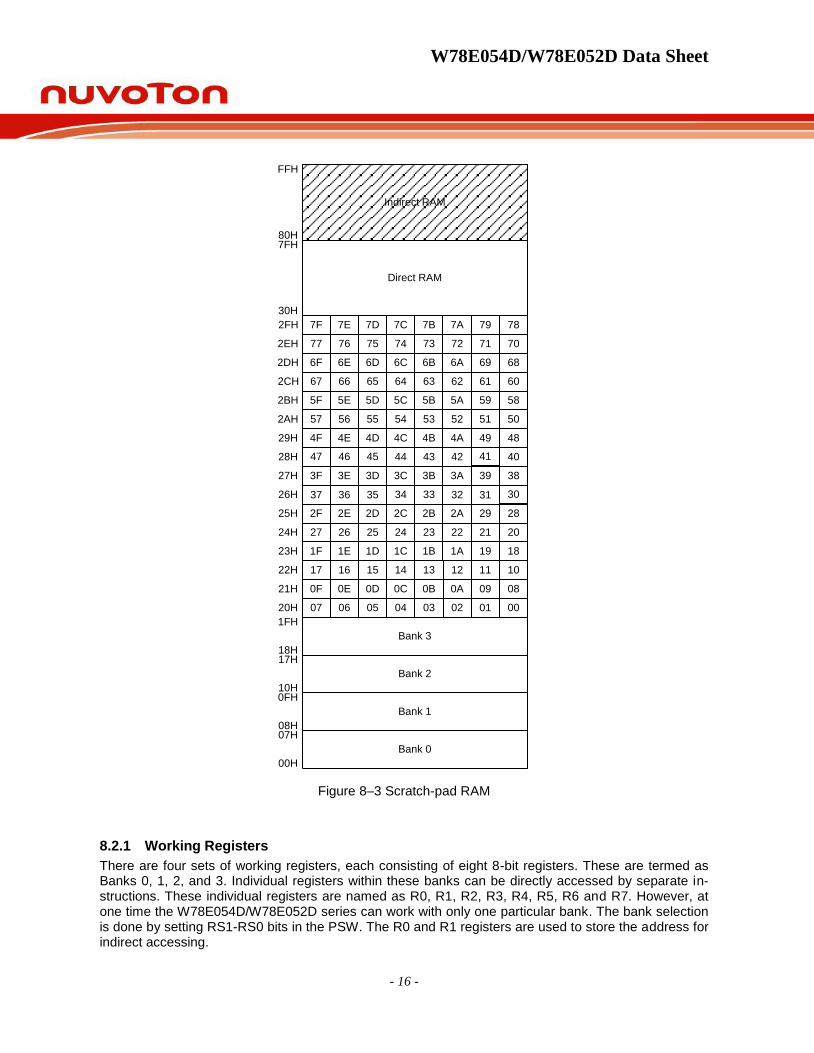
Figure 8–3 Scratch-pad RAM
8.2.1 Working Registers
There are four sets of working registers, each consisting of eight 8-bit registers. These are termed as Banks 0, 1, 2, and 3. Individual registers within these banks can be directly accessed by separate in-structions. These individual registers are named as R0, R1, R2, R3, R4, R5, R6 and R7. However, at one time the W78E054D/W78E052D series can work with only one particular bank. The bank selection is done by setting RS1-RS0 bits in the PSW. The R0 and R1 registers are used to store the address for indirect accessing.

W78E054D/W78E052D Data Sheet
Publication Release Date: Aug 31, 2012
- 17 - Revision A12
8.2.2 Bit addressable Locations
The Scratch-pad RAM area from location 20h to 2Fh is byte as well as bit addressable. This means that a bit in this area can be individually addressed. In addition some of the SFRs are also bit address-able. The instruction decoder is able to distinguish a bit access from a byte access by the type of the instruction itself. In the SFR area, any existing SFR whose address ends in a 0 or 8 is bit addressable.
8.2.3 Stack
The scratch-pad RAM can be used for the stack. This area is selected by the Stack Pointer (SP), which stores the address of the top of the stack. Whenever a jump, call or interrupt is invoked the return ad-dress is placed on the stack. There is no restriction as to where the stack can begin in the RAM. By default however, the Stack Pointer contains 07h at reset. The user can then change this to any value desired. The SP will point to the last used value. Therefore, the SP will be incremented and then ad-dress saved onto the stack. Conversely, while popping from the stack the contents will be read first, and then the SP is decreased.

W78E054D/W78E052D Data Sheet
- 18 -
9 SPECIAL FUNCTION REGISTERS
The W78E054D/W78E052D series uses Special Function Registers (SFRs) to control and monitor pe-ripherals and their Modes. The SFRs reside in the register locations 80-FFh and are accessed by direct addressing only. Some of the SFRs are bit addressable. This is very useful in cases where users wish to modify a particular bit without changing the others. The SFRs that are bit addressable are those whose addresses end in 0 or 8. The W78E054D/W78E052D series contain all the SFRs present in the standard 8052. However some additional SFRs are added. In some cases the unused bits in the origi-nal 8052, have been given new functions. The list of the SFRs is as follows.
F8 FF
F0 B F7
E8 EF
E0 ACC E7
D8 P4 DF
D0 PSW D7
C8 T2CON T2MOD RCAP2L RCAP2H TL2 TH2 CF
C0 XICON SFRAL SFRAH SFRRD SFRCN C7
B8 IP EAPAGE CHPCON BF
B0 P3 IPH B7
A8 IE AF
A0 P2 A7
98 SCON SBUF 9F
90 P1 97
88 TCON TMOD TL0 TL1 TH0 TH1 AUXR WDTC 8F
80 P0 SP DPL DPH P0UPR PCON 87
Table 9–1: Special Function Register Location Table
Note:
1. The SFRs in the column with dark borders are bit-addressable
2. The table is condensed with eight locations per row. Empty locations indicate that these are no regis-ters at these addresses. When a bit or register is not implemented, it will read high.

W78E054D/W78E052D Data Sheet
Publication Release Date: Aug 31, 2012
- 19 - Revision A12
Special Function Registers:
SYMBOL DEFINITION ADDRESS MSB BIT ADDRESS, SYMBOL LSB RESET
B B register F0H (F7) (F6) (F5) (F4) (F3) (F2) (F1) (F0) 0000 0000B
ACC Accumulator E0H (E7) (E6) (E5) (E4) (E3) (E2) (E1) (E0) 0000 0000B
P4 Port 4 D8H INT2 INT3 0000 1111B
PSW Program status word D0H (D7)
CY
(D6)
AC
(D5)
F0
(D4)
RS1
(D3)
RS0
(D2)
OV
(D1)
F1
(D0)
P
0000 0000B
TH2 T2 reg. high CDH 0000 0000B
TL2 T2 reg. low CCH 0000 0000B
RCAP2H T2 capture low CBH 0000 0000B
RCAP2L T2 capture high CAH 0000 0000B
T2MOD Timer 2 Mode C9 DCEN 0000 0000B
T2CON Timer 2 control C8H (CF)
TF2
(CE)
EXF2
(CD)
RCLK
(CC)
TCLK
(CB)
EXEN2
(CA)
TR2
(C9)
C/T2
(C8)
CP/RL2
0000 0000B
SFRCN SFR program of control C7H NOE NCE CTRL3 CTRL2 CTRL1 CTRL0 0000 0000B
SFRRD SFR program of data register C6H 0000 0000B
SFRAH SFR program of address high byte C5H 0000 0000B
SFRAL SFR program of address low byte C4H 0000 0000B
XICON External interrupt control C0H PX3 EX3 IE3 IT3 PX2 EX2 IE2 IT2 0000 0000B
CHPCON Chip control BFH SWRST - - - - ISP ENP 0000 0000B
EAPAGE Erase page operation modes BEH EAPG1 EAPG0 0000 0000B
IP Interrupt priority B8H (BF)
-
(BE)
-
(BD)
PT2
(BC)
PS
(BB)
PT1
(BA)
PX1
(B9)
PT0
(B8)
PX0
1100 0000B
IPH Interrupt priority High B7H 0000 0000B
P3 Port 3 B0H (B7)
RD
(B6)
WR
(B5)
T1
(B4)
T0
(B3)
INT1
(B2)
INT0
(B1)
TXD
(B0)
RXD
1111 1111B
IE Interrupt enable A8H (AF)
EA
(AE)
-
(AD)
ET2
(AC)
ES
(AB)
ET1
(AA)
EX1
(A9)
ET0
(A8)
EX0
0100 0000B
P2 Port 2 A0H (A7)
A15
(A6)
A14
(A5)
A13
(A4)
A12
(A3)
A11
(A2)
A10
(A1)
A9
(A0)
A8
1111 1111B
SBUF Serial buffer 99H 0000 0000B
SCON Serial control 98H (9F)
SM0/FE
(9E)
SM1
(9D)
SM2
(9C)
REN
(9B)
TB8
(9A)
RB8
(99)
TI
(98)
RI
0000 0000B
P1 Port 1 90H (97)
(96)
(95)
(94)
(93)
(92)
(91)
T2EX
(90)
T2
1111 1111B
WDTC Watchdog control 8FH ENW CLRW WIDL - - PS2 PS1 PS0 0000 0000B
AUXR Auxiliary 8EH - - - - ALEOFF 0000 0110B
TH1 Timer high 1 8DH 0000 0000B
TH0 Timer high 0 8CH 0000 0000B
TL1 Timer low 1 8BH 0000 0000B
TL0 Timer low 0 8AH 0000 0000B
TMOD Timer mode 89H GATE C/T M1 M0 GATE C/T M1 M0 0000 0000B
TCON Timer control 88H (8F)
TF1
(8E)
TR1
(8D)
TF0
(8C)
TR0
(8B)
IE1
(8A)
IT1
(89)
IE0
(88)
IT0
0000 0000B
PCON Power control 87H SMOD SMOD0 - POR GF1 GF0 PD IDL 0011 0000B
P0UPR Port 0 pull up option Register 86H - - - - - - - P0UP 0000 0001B
DPH Data pointer high 83H 0000 0000B
DPL Data pointer low 82H 0000 0000B

W78E054D/W78E052D Data Sheet
- 20 -
SP Stack pointer 81H 0000 0111B
P0 Port 0 80H (87) (86) (85) (84) (83) (82) (81) (80) 1111 1111B
9.1 SFR Detail Bit Descriptions
Port 0
Bit: 7 6 5 4 3 2 1 0
P0.7 P0.6 P0.5 P0.4 P0.3 P0.2 P0.1 P0.0
Mnemonic: P0 Address: 80h
BIT NAME FUNCTION
7-0 P0.[7:0] Port 0 is an open-drain bi-directional I/O port if SFR P0UPR.0 (bit P0UP) clear to “0”, and
when SFR P0UPR.0 (bit P0UP) set to “1”, Port 0 pins are internally pulled-up.
This port also provides a multiplexed low order address/data bus during accesses to external memory.
STACK POINTER
Bit: 7 6 5 4 3 2 1 0
SP.7 SP.6 SP.5 SP.4 SP.3 SP.2 SP.1 SP.0
Mnemonic: SP Address: 81h
BIT NAME FUNCTION
7-0 SP.[7:0] The Stack Pointer stores the Scratch-pad RAM address where the stack begins. In other words it always points to the top of the stack.
DATA POINTER LOW
Bit: 7 6 5 4 3 2 1 0
DPL.7 DPL.6 DPL.5 DPL.4 DPL.3 DPL.2 DPL.1 DPL.0
Mnemonic: DPL Address: 82h
BIT NAME FUNCTION
7-0 DPL.[7:0] This is the low byte of the standard 8052 16-bit data pointer.
DATA POINTER HIGH
Bit: 7 6 5 4 3 2 1 0
DPH.7 DPH.6 DPH.5 DPH.4 DPH.3 DPH.2 DPH.1 DPH.0
Mnemonic: DPH Address: 83h
BIT NAME FUNCTION
7-0 DPH.[7:0] This is the high byte of the standard 8052 16-bit data pointer.
Port 0 Pull Up Option Register
Bit: 7 6 5 4 3 2 1 0

W78E054D/W78E052D Data Sheet
Publication Release Date: Aug 31, 2012
- 21 - Revision A12
- - - - - - - P0UP
Mnemonic: P0UPR Address: 86h
BIT NAME FUNCTION
0 P0UP 0: Port 0 pins are open-drain.
1: Port 0 pins are internally pulled-up. Port 0 is structurally the same as Port 2.
Power Control
Bit: 7 6 5 4 3 2 1 0
SMOD SMOD0 - POR GF1 GF0 PD IDL
Mnemonic: PCON Address: 87h
BIT NAME FUNCTION
7 SMOD 1: This bit doubles the serial port baud rate in mode 1, 2, and 3 when set to 1.
6 SMOD0
0: Framing Error Detection Disable. SCON.7 (SM0/FE) bit is used as SM0 (stand-ard 8052 function).
1: Framing Error Detection Enable. SCON.7 (SM0/FE) bit is used to reflect as Frame Error (FE) status flag.
5 - Reserved
4 POR 0: Cleared by software.
1: Set automatically when a power-on reset has occurred.
3 GF1 General purpose user flags.
2 GF0 General purpose user flags.
1 PD 1: The CPU goes into the POWER DOWN mode. In this mode, all the clocks are stopped and program execution is frozen.
0 IDL 1: The CPU goes into the IDLE mode. In this mode, the clocks CPU clock stopped, so program execution is frozen. But the clock to the serial, timer and interrupt blocks is not stopped, and these blocks continue operating.
Timer Control
Bit: 7 6 5 4 3 2 1 0
TF1 TR1 TF0 TR0 IE1 IT1 IE0 IT0
Mnemonic: TCON Address: 88h
BIT NAME FUNCTION
7 TF1 Timer 1 Overflow Flag. This bit is set when Timer 1 overflows. It is cleared auto-matically when the program does a timer 1 interrupt service routine. Software can also set or clear this bit.
6 TR1 Timer 1 Run Control. This bit is set or cleared by software to turn timer/counter on or off.
5 TF0 Timer 0 Overflow Flag. This bit is set when Timer 0 overflows. It is cleared auto-matically when the program does a timer 0 interrupt service routine. Software can
W78E054D/W78E052D Data Sheet
- 22 -
also set or clear this bit.
4 TR0 Timer 0 Run Control. This bit is set or cleared by software to turn timer/counter on or off.
3 IE1 Interrupt 1 Edge Detect Flag: Set by hardware when an edge/level is detected on
1INT . This bit is cleared by hardware when the service routine is vectored to only if the interrupt was edge triggered. Otherwise it follows the inverse of the pin.
2 IT1 Interrupt 1 Type Control. Set/cleared by software to specify falling edge/ low level triggered external inputs.
1 IE0 Interrupt 0 Edge Detect Flag. Set by hardware when an edge/level is detected
on 0INT . This bit is cleared by hardware when the service routine is vectored to
only if the interrupt was edge triggered. Otherwise it follows the inverse of the pin.
0 IT0 Interrupt 0 Type Control: Set/cleared by software to specify falling edge/ low level triggered external inputs.
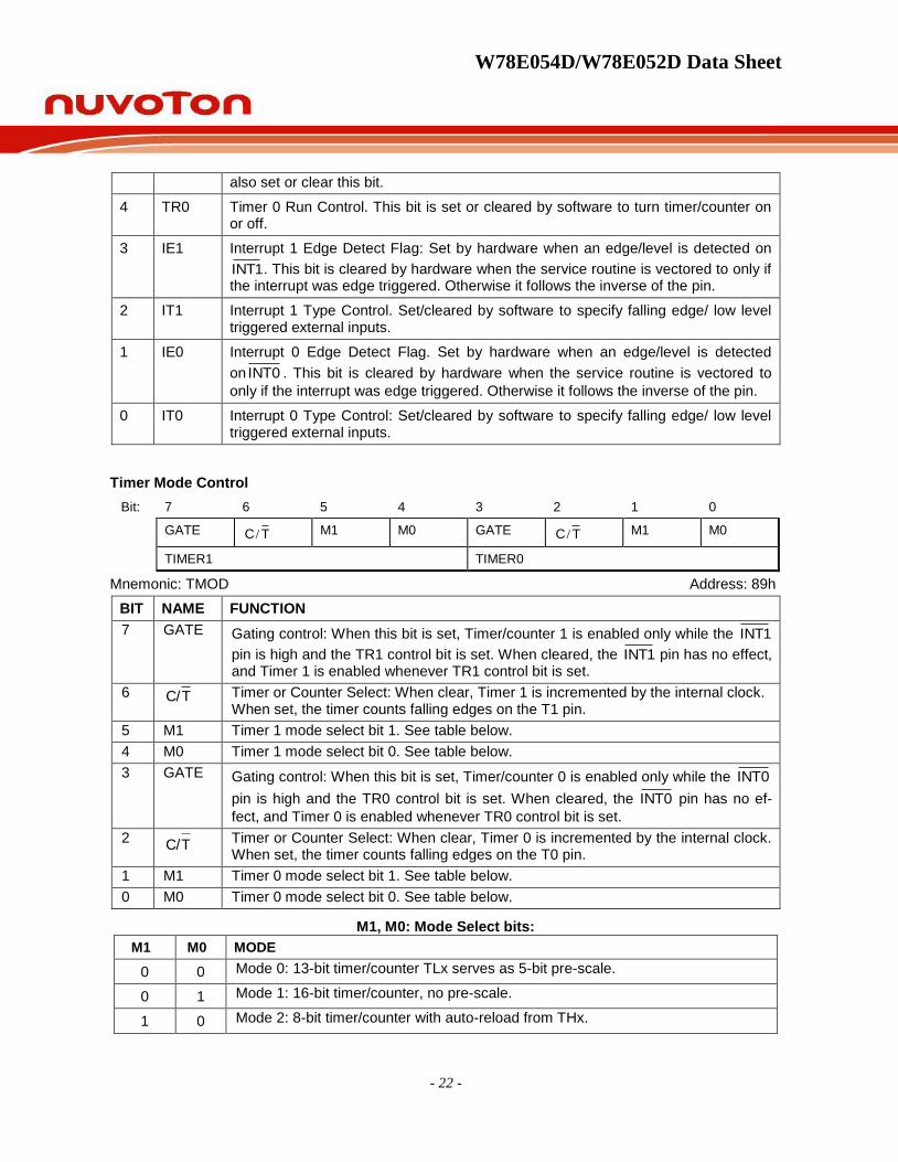
Timer Mode Control
Bit: 7 6 5 4 3 2 1 0
GATE TC / M1 M0 GATE TC /
M1 M0
TIMER1 TIMER0
Mnemonic: TMOD Address: 89h
BIT NAME FUNCTION
7 GATE Gating control: When this bit is set, Timer/counter 1 is enabled only while the 1INT
pin is high and the TR1 control bit is set. When cleared, the 1INT pin has no effect, and Timer 1 is enabled whenever TR1 control bit is set.
6 TC/ Timer or Counter Select: When clear, Timer 1 is incremented by the internal clock. When set, the timer counts falling edges on the T1 pin.
5 M1 Timer 1 mode select bit 1. See table below.
4 M0 Timer 1 mode select bit 0. See table below.
3 GATE Gating control: When this bit is set, Timer/counter 0 is enabled only while the 0INT
pin is high and the TR0 control bit is set. When cleared, the 0INT pin has no ef-
fect, and Timer 0 is enabled whenever TR0 control bit is set.
2 TC/ Timer or Counter Select: When clear, Timer 0 is incremented by the internal clock. When set, the timer counts falling edges on the T0 pin.
1 M1 Timer 0 mode select bit 1. See table below.
0 M0 Timer 0 mode select bit 0. See table below.
M1, M0: Mode Select bits:
M1 M0 MODE
0 0 Mode 0: 13-bit timer/counter TLx serves as 5-bit pre-scale.
0 1 Mode 1: 16-bit timer/counter, no pre-scale.
1 0 Mode 2: 8-bit timer/counter with auto-reload from THx.

W78E054D/W78E052D Data Sheet
Publication Release Date: Aug 31, 2012
- 23 - Revision A12
1 1 Mode 3: (Timer 0) TL0 is an 8-bit timer/counter controlled by the standard Timer0 control bits. TH0 is an 8-bit timer only controlled by Timer1 control bits. (Timer 1) Timer/Counter 1 is stopped.
Timer 0 LSB
Bit: 7 6 5 4 3 2 1 0
TL0.7 TL0.6 TL0.5 TL0.4 TL0.3 TL0.2 TL0.1 TL0.0
Mnemonic: TL0 Address: 8Ah
BIT NAME FUNCTION
7-0 TL0.[7:0] Timer 0 LSB.
Timer 1 LSB
Bit: 7 6 5 4 3 2 1 0
TL1.7 TL1.6 TL1.5 TL1.4 TL1.3 TL1.2 TL1.1 TL1.0
Mnemonic: TL1 Address: 8Bh
BIT NAME FUNCTION
7-0 TL1.[7:0] Timer 1 LSB.
Timer 0 MSB
Bit: 7 6 5 4 3 2 1 0
TH0.7 TH0.6 TH0.5 TH0.4 TH0.3 TH0.2 TH0.1 TH0.0
Mnemonic: TH0 Address: 8Ch
BIT NAME FUNCTION
7-0 TH0.[7:0] Timer 0 MSB.
Timer 1 MSB
Bit: 7 6 5 4 3 2 1 0
TH1.7 TH1.6 TH1.5 TH1.4 TH1.3 TH1.2 TH1.1 TH1.0
Mnemonic: TH1 Address: 8Dh
BIT NAME FUNCTION
7-0 TH1.[7:0] Timer 1 MSB.
AUXR
Bit: 7 6 5 4 3 2 1 0
- - - - - - - ALE_OFF

W78E054D/W78E052D Data Sheet
- 24 -
Mnemonic: AUXR Address: 8Eh
BIT NAME FUNCTION
0 ALE_OFF 1: Disenable ALE output
0: Enable ALE output
Watchdog Timer Control Register
Bit: 7 6 5 4 3 2 1 0
ENW CLRW WIDL - - PS2 PS1 PS0
Mnemonic: WDTC Address: 8FH
BIT NAME FUNCTION
7 ENW Enable watch-dog if set.
6 CLRW Clear watch-dog timer and Pre-scalar if set. This flag will be cleared automatical-ly.
5 WIDL If this bit is set, watch-dog is enabled under IDLE mode. If cleared, watch-dog is disabled under IDLE mode. Default is cleared.
2-0 PS2-0 Watch-dog Pre-scalar timer select. Pre-scalar is selected when set PS20 as fol-lows:
PS2 PS1 PS0 PRE-SCALAR SELECT
0 0 0 2
0 0 1 8
0 1 0 4
0 1 1 16
1 0 0 32
1 0 1 64
1 1 0 128
1 1 1 256
Port 1
Bit: 7 6 5 4 3 2 1 0
P1.7 P1.6 P1.5 P1.4 P1.3 P1.2 P1.1 P1.0
Mnemonic: P1 Address: 90h
BIT NAME FUNCTION
7-0 P1.[7:0] General purpose I/O port. Most instructions will read the port pins in case of a port read access, however in case of read-modify-write instructions, the port latch is read.
Serial Port Control

W78E054D/W78E052D Data Sheet
Publication Release Date: Aug 31, 2012
- 25 - Revision A12
Bit: 7 6 5 4 3 2 1 0
SM0/FE SM1 SM2 REN TB8 RB8 TI RI
Mnemonic: SCON Address: 98h
BIT NAME FUNCTION
7 SM0/FE Serial port mode select bit 0 or Framing Error Flag: The SMOD0 bit in PCON SFR determines whether this bit acts as SM0 or as FE. The operation of SM0 is described below. When used as FE, this bit will be set to indicate an invalid stop bit. This bit must be manually cleared in software to clear the FE condition.
6 SM1 Serial Port mode select bit 1. See table below.
5 SM2 Multiple processors communication. Setting this bit to 1 enables the multiproces-sor communication feature in mode 2 and 3. In mode 2 or 3, if SM2 is set to 1, then RI will not be activated if the received 9th data bit (RB8) is 0. In mode 1, if SM2 = 1, then RI will not be activated if a valid stop bit was not received. In mode 0, the SM2 bit controls the serial port clock. If set to 0, then the serial port runs at a divide by 12 clock of the oscillator. This gives compatibility with the standard 8052. When set to 1, the serial clock become divide by 4 of the oscilla-tor clock. This results in faster synchronous serial communication.
4 REN Receive enable:
0: Disable serial reception.
1: Enable serial reception.
3 TB8 This is the 9th bit to be transmitted in modes 2 and 3. This bit is set and cleared by software as desired.
2 RB8 In modes 2 and 3 this is the received 9th data bit. In mode 1, if SM2 = 0, RB8 is the stop bit that was received. In mode 0 it has no function.
1 TI Transmit interrupt flag: This flag is set by hardware at the end of the 8th bit time in mode 0, or at the beginning of the stop bit in all other modes during serial transmission. This bit must be cleared by software.
0 RI
Receive interrupt flag: This flag is set by hardware at the end of the 8th bit time in mode 0, or halfway through the stop bits time in the other modes during serial reception. However the restrictions of SM2 apply to this bit. This bit can be cleared only by software.
SM1, SM0: Mode Select bits:
Mode SM0 SM1 Description Length Baud Rate
0 0 0 Synchronous 8 Tclk divided by 4 or 12
1 0 1 Asynchronous 10 Variable
2 1 0 Asynchronous 11 Tclk divided by 32 or 64
3 1 1 Asynchronous 11 Variable
Serial Data Buffer

W78E054D/W78E052D Data Sheet
- 26 -
Bit: 7 6 5 4 3 2 1 0
SBUF.7 SBUF.6 SBUF.5 SBUF.4 SBUF.3 SBUF.2 SBUF.1 SBUF.0
Mnemonic: SBUF Address: 99h
BIT NAME FUNCTION
7~0 SBUF Serial data on the serial port is read from or written to this location. It actually consists of two separate internal 8-bit registers. One is the receive resister, and the other is the transmit buffer. Any read access gets data from the receive data buffer, while write access is to the transmit data buffer.
Port 2
Bit: 7 6 5 4 3 2 1 0
P2.7 P2.6 P2.5 P2.4 P2.3 P2.2 P2.1 P2.0
Mnemonic: P2 Address: A0h
BIT NAME FUNCTION
7-0 P2.[7:0] Port 2 is a bi-directional I/O port with internal pull-ups. This port also provides the upper address bits for accesses to external memory.
Interrupt Enable
Bit: 7 6 5 4 3 2 1 0
EA - ET2 ES ET1 EX1 ET0 EX0
Mnemonic: IE Address: A8h
BIT NAME FUNCTION
7 EA Global enable. Enable/Disable all interrupts.
6 - Reserved
5 ET2 Enable Timer 2 interrupt.
4 ES Enable Serial Port 0 interrupt.
3 ET1 Enable Timer 1 interrupt.
2 EX1 Enable external interrupt 1.
1 ET0 Enable Timer 0 interrupt.
0 EX0 Enable external interrupt 0.
Port 3
Bit: 7 6 5 4 3 2 1 0
P3.7 P3.6 P3.5 P3.4 P3.3 P3.2 P3.1 P3.0
Mnemonic: P3 Address: B0h
P3.7-0: General purpose Input/Output port. Most instructions will read the port pins in case of a port read access, however in case of read-modify-write instructions, the port latch is read. These alter-nate functions are described below:

W78E054D/W78E052D Data Sheet
Publication Release Date: Aug 31, 2012
- 27 - Revision A12
BIT NAME FUNCTION
7 P3.7 RD
6 P3.6 WR
5 P3.5 T1
4 P3.4 T0
3 P3.3 INT1
2 P3.2 INT0
1 P3.1 TX
0 P3.0 RX
Interrupt High Priority
Bit: 7 6 5 4 3 2 1 0
IPH.7 IPH.6 IPH.5 IPH.4 IPH.3 IPH.2 IPH.1 IPH.0
Mnemonic: IPH Address: B7h
BIT NAME FUNCTION
7 IPH.7 1: Interrupt high priority of INT3 is highest priority level.
6 IPH.6 1: Interrupt high priority of INT2 is highest priority level.
5 IPH.5 1: Interrupt high priority of Timer 2 is highest priority level.
4 IPH.4 1: Interrupt high priority of Serial Port 0 is highest priority level.
3 IPH.3 1: Interrupt high priority of Timer 1 is highest priority level.
2 IPH.2 1: Interrupt high priority of External interrupt 1 is highest priority level.
1 IPH.1 1: Interrupt high priority of Timer 0 is highest priority level.
0 IPH.0 1: Interrupt high priority of External interrupt 0 is highest priority level.
Interrupt Priority
Bit: 7 6 5 4 3 2 1 0
- - PT2 PS PT1 PX1 PT0 PX0
Mnemonic: IP Address: B8h
BIT NAME FUNCTION
5 PT2 1: Interrupt priority of Timer 2 is higher priority level.
4 PS 1: Interrupt priority of Serial port 0 is higher priority level.
3 PT1 1: Interrupt priority of Timer 1 is higher priority level.
2 PX1 1: Interrupt priority of External interrupt 1 is higher priority level.
1 PT0 1: Interrupt priority of Timer 0 is higher priority level.

W78E054D/W78E052D Data Sheet
- 28 -
0 PX0 1: Interrupt priority of External interrupt 0 is higher priority level.
EAPAGE ERASE PAGE Operation Modes
Bit: 7 6 5 4 3 2 1 0
- - - - - - EAPG1 EAPG0
Mnemonic: EAPAGE Address: BD
BIT NAME FUNCTION
1 EAPG1 1: To ease PAGE1 when ease command is set. (LDROM)
0 EAPG0 1: To ease PAGE0 when ease command is set. (APROM)
;CPU Clock = 12MHz/12T mode
READ_TIME EQU 1
PROGRAM_TIME EQU 50
ERASE_TIME EQU 5000
Erase_APROM:
mov EAPAGE,#01h ;set EAPAGE is APROM
mov SFRCN,#ERASE_ROM
mov TL0,#LOW (65536-ERASE_TIME)
mov TH0,#HIGH(65536-ERASE_TIME)
setb TR0
mov CHPCON,#00000011b
mov EAPAGE,#00h ;clear EAPAGE
clr TF0
clr TR0
ret
Erase_LDROM:
mov EAPAGE,#02h ;set EAPAGE is LDROM
mov SFRCN,#ERASE_ROM
mov TL0,#LOW (65536-ERASE_TIME)
mov TH0,#HIGH(65536-ERASE_TIME)
setb TR0
mov CHPCON,#00000011b
mov EAPAGE,#00h ;clear EAPAGE
clr TF0
clr TR0
ret
Chip Control
Bit: 7 6 5 4 3 2 1 0

W78E054D/W78E052D Data Sheet
Publication Release Date: Aug 31, 2012
- 29 - Revision A12
SWRST - - - - - ISP ENP
Mnemonic: CHPCON Address: BFh
Bit Name Function
7 SWRST When this bit is set to 1 and ENP is set to 1. It will enforce microcontroller reset to initial condition just like power on reset. This action will re-boot the microcontroller and start to normal operation.
1 ISP The ISP function Select. When this bit is set to 1 and ENP is set to 1. It will run ISP function.
0 ENP When this bit is set to 1 and SWRST is set to 1. It will enforce microcontrol-ler reset to initial condition just like power on reset.
When this bit is set to 1 and ISP is set to 1. It will run ISP function
Note1: CHPCON = 0x81, it is Software reset
Note2: CHPCON = 0x03, ISP function is enabled.
External Interrupt Control
Bit: 7 6 5 4 3 2 1 0
PX3 EX3 IE3 IT3 PX2 EX2 IE2 IT2
Mnemonic: XICON Address: C0h
BIT NAME FUNCTION
7 PX3 External interrupt 3 priority is higher if set this bit to 1
6 EX3 Enable External interrupt 3 if set this bit to 1
5 IE3 If IT3 = 1, IE3 is set/cleared automatically by hardware when interrupt is detect-ed/serviced
4 IT3 External interrupt 3 is falling-edge/low-level triggered when this bit is set/cleared by software
3 PX2 External interrupt 2 priority is higher if set this to 1
2 EX2 Enable External interrupt 2 if set this bit to 1
1 IE2 If IT2 = 1, IE2 is set/cleared automatically by hardware when interrupt is detect-ed/serviced
0 IT2 External interrupt 2 is falling-edge/low-level triggered when this bit is set/cleared by software
SFR program of address low
Bit: 7 6 5 4 3 2 1 0
SFRAL.7 SFRAL.6 SFRAL.5 SFRAL.4 SFRAL.3 SFRAL.2 SFRAL.1 SFRAL.0
Mnemonic: SFRAL Address: C4h
BIT NAME FUNCTION
7-0 SFRAL.[7:0] The programming address of on-chip flash memory in programming mode.

W78E054D/W78E052D Data Sheet
- 30 -
SFRFAL contains the low-order byte of address.
SFR program of address high
Bit: 7 6 5 4 3 2 1 0
SFRAH.7 SFRAH.6 SFRAH.5 SFRAH.4 SFRAH.3 SFRAH.2 SFRAH.1 SFRAH.0
Mnemonic: SFRAH Address: C5h
BIT NAME FUNCTION
7-0 SFRAH.[7:0] The programming address of on-chip flash memory in programming mode. SFRFAH contains the high-order byte of address.
SFR program For Data
Bit: 7 6 5 4 3 2 1 0
SFRFD.7 SFRFD.6 SFRFD.5 SFRFD.4 SFRFD.3 SFRFD.2 SFRFD.1 SFRFD.0
Mnemonic: SFRFD Address: C6h
BIT NAME FUNCTION
7-0 SFRFD.[7:0] The programming data for on-chip flash memory in programming mode.
SFR for Program Control
Bit: 7 6 5 4 3 2 1 0
- OEN CEN CTRL3 CTRL2 CTRL1 CTRL0
Mnemonic: SFRCN Address: C7h
BIT NAME FUNCTION
5 OEN FLASH EPROM output enable.
4 CEN FLASH EPROM chip enable.
3-0 CTRL[3:0] CTRL[3:0]: The flash control signals
Mode OEN CEN CTRL<3:0> SFRAH, SFRAL SFRFD
Flash Standby 1 1 X X X
Read Company ID 0 0 1011 0FFh, 0FFh Data out
Read Device ID High 0 0 1100 0FFh, 0FFh Data out
Read Device ID Low 1 0 1100 0FFh, 0FEh Data out
Erase APROM 1 0 0010 X X
Erase Verify APROM 0 0 1001 Address in Data out
Program APROM 1 0 0001 Address in Data in
Program Verify APROM 0 0 1010 Address in Data out
Read APROM 0 0 0000 Address in Data out

W78E054D/W78E052D Data Sheet
Publication Release Date: Aug 31, 2012
- 31 - Revision A12
Timer 2 Control
Bit: 7 6 5 4 3 2 1 0
TF2 EXF2 RCLK TCLK EXEN2 TR2 C T/ 2 CP RL/ 2
Mnemonic: T2CON Address: C8h
BIT NAME FUNCTION
7 TF2 Timer 2 overflow flag: This bit is set when Timer 2 overflows. It is also set when the count is equal to the capture register in down count mode. It can be set only if RCLK and TCLK are both 0. It is cleared only by software. Software can also set or clear this bit.
6 EXF2 Timer 2 External Flag: A negative transition on the T2EX pin (P1.1) or timer 2
overflow will cause this flag to set based on the CP RL/ 2 , EXEN2 and DCEN bits. If set by a negative transition, this flag must be cleared by software. Set-ting this bit in software or detection of a negative transition on T2EX pin will force a timer interrupt if enabled.
5 RCLK Receive Clock Flag: This bit determines the serial port 0 time-base when re-ceiving data in serial modes 1 or 3. If it is 0, then timer 1 overflow is used for baud rate generation, otherwise timer 2 overflow is used. Setting this bit forces timer 2 in baud rate generator mode.
4 TCLK Transmit Clock Flag: This bit determines the serial port 0 time-base when transmitting data in modes 1 and 3. If it is set to 0, the timer 1 overflow is used to generate the baud rate clock otherwise timer 2 overflow is used. Setting this bit forces timer 2 in baud rate generator mode.
3 EXEN2 Timer 2 External Enable. This bit enables the capture/reload function on the T2EX pin if Timer 2 is not generating baud clocks for the serial port. If this bit is 0, then the T2EX pin will be ignored, otherwise a negative transition detect-ed on the T2EX pin will result in capture or reload.
2 TR2 Timer 2 Run Control. This bit enables/disables the operation of timer 2. Clear-ing this bit will halt the timer 2 and preserve the current count in TH2, TL2.
1 C T/ 2 Counter/Timer Select. This bit determines whether timer 2 will function as a timer or a counter. Independent of this bit, the timer will run at 2 clocks per tick when used in baud rate generator mode.
0 CP RL/ 2 Capture/Reload Select. This bit determines whether the capture or reload function will be used for timer 2. If either RCLK or TCLK is set, this bit will be ignored and the timer will function in an auto-reload mode following each over-flow. If the bit is 0 then auto-reload will occur when timer 2 overflows or a fall-ing edge is detected on T2EX pin if EXEN2 = 1. If this bit is 1, then timer 2 captures will occur when a falling edge is detected on T2EX pin if EXEN2 = 1.
Timer 2 Mode Control
Bit: 7 6 5 4 3 2 1 0
- - - - - - DCEN

W78E054D/W78E052D Data Sheet
- 32 -
Mnemonic: T2MOD Address: C9h
BIT NAME FUNCTION
0 DCEN Down Count Enable: This bit, in conjunction with the T2EX pin, controls the direction that timer 2 counts in 16-bit auto-reload mode.
Timer 2 Capture LSB
Bit: 7 6 5 4 3 2 1 0
RCAP2L.7 RCAP2L.6 RCAP2L.5 RCAP2L.4 RCAP2L.3 RCAP2L.2 RCAP2L.1 RCAP2L.0
Mnemonic: RCAP2L Address: CAh
BIT NAME FUNCTION
7-0 RCAP2L.[7:0] This register is used to capture the TL2 value when a timer 2 is configured in capture mode. RCAP2L is also used as the LSB of a 16-bit reload value when timer 2 is configured in auto-reload mode.
Timer 2 Capture MSB
Bit: 7 6 5 4 3 2 1 0
RCAP2h.7 RCAP2h.6 RCAP2h.5 RCAP2h.4 RCAP2h.3 RCAP2h.2 RCAP2h.1 RCAP2h.0
Mnemonic: RCAP2H Address: CBh
BIT NAME FUNCTION
7-0 RCAP2H.[7:0] This register is used to capture the TH2 value when a timer 2 is configured in capture mode. RCAP2H is also used as the MSB of a 16-bit reload value when timer 2 is configured in auto-reload mode.
Timer 2 LSB
Bit: 7 6 5 4 3 2 1 0
TL2.7 TL2.6 TL2.5 TL2.4 TL2.3 TL2.2 TL2.1 TL2.0
Mnemonic: TL2 Address: CCh
BIT NAME FUNCTION
7-0 TL2.[7:0] Timer 2 LSB
Timer 2 MSB
Bit: 7 6 5 4 3 2 1 0
TH2.7 TH2.6 TH2.5 TH2.4 TH2.3 TH2.2 TH2.1 TH2.0
Mnemonic: TH2 Address: CDh
BIT NAME FUNCTION
7-0 TH2.[7:0] Timer 2 MSB

W78E054D/W78E052D Data Sheet
Publication Release Date: Aug 31, 2012
- 33 - Revision A12
Program Status Word
Bit: 7 6 5 4 3 2 1 0
CY AC F0 RS1 RS0 OV F1 P
Mnemonic: PSW Address: D0h
BIT NAME FUNCTION
7 CY Carry flag:
Set for an arithmetic operation which results in a carry being generated from the ALU. It is also used as the accumulator for the bit operations.
6 AC Auxiliary carry:
Set when the previous operation resulted in a carry from the high order nibble.
5 F0 User flag 0:
The General purpose flag that can be set or cleared by the user.
4 RS1 Register bank select bits:
3 RS0 Register bank select bits:
2 OV Overflow flag:
Set when a carry was generated from the seventh bit but not from the 8th bit as a
result of the previous operation, or vice-versa.
1 F1 User Flag 1:
The General purpose flag that can be set or cleared by the user by software.
0 P Parity flag:
Set/cleared by hardware to indicate odd/even number of 1’s in the accumulator.
Port 4
Bit: 7 6 5 4 3 2 1 0
- - - - P4.3 P4.2 P4.1 P4.0
Mnemonic: P4 Address: D8h
Another bit-addressable port P4 is also available and only 4 bits (P4<3:0>) can be used. This port ad-dress is located at 0D8H with the same function as that of port P1, except the P4.3 and P4.2 are alter-
native function pins. It can be used as general I/O pins or external interrupt input sources ( INT2 ,
INT3 ).
ACCUMULATOR
Bit: 7 6 5 4 3 2 1 0
ACC.7 ACC.6 ACC.5 ACC.4 ACC.3 ACC.2 ACC.1 ACC.0
Mnemonic: ACC Address: E0h
Bit Name Function
7-0 ACC The A or ACC register is the standard 8052 accumulator.
B Register

W78E054D/W78E052D Data Sheet
- 34 -
Bit: 7 6 5 4 3 2 1 0
B.7 B.6 B.5 B.4 B.3 B.2 B.1 B.0
Mnemonic: B Address: F0h
Bit Name Function
7-0 B The B register is the standard 8052 register that serves as a second accumulator.

W78E054D/W78E052D Data Sheet
Publication Release Date: Aug 31, 2012
- 35 - Revision A12
10 INSTRUCTION
The W78E054D/W78E052D series execute all the instructions of the standard 8052 family. The opera-tions of these instructions, as well as their effects on flag and status bits, are exactly the same.
Op-code HEX Code Bytes W78E054D/W78E052D series Clock
cycles
NOP 00 1 12
ADD A, R0 28 1 12
ADD A, R1 29 1 12
ADD A, R2 2A 1 12
ADD A, R3 2B 1 12
ADD A, R4 2C 1 12
ADD A, R5 2D 1 12
ADD A, R6 2E 1 12
ADD A, R7 2F 1 12
ADD A, @R0 26 1 12
ADD A, @R1 27 1 12
ADD A, direct 25 2 12
ADD A, #data 24 2 12
ADDC A, R0 38 1 12
ADDC A, R1 39 1 12
ADDC A, R2 3A 1 12
ADDC A, R3 3B 1 12
ADDC A, R4 3C 1 12
ADDC A, R5 3D 1 12
ADDC A, R6 3E 1 12
ADDC A, R7 3F 1 12
ADDC A, @R0 36 1 12
ADDC A, @R1 37 1 12
ADDC A, direct 35 2 12
ADDC A, #data 34 2 12
SUBB A, R0 98 1 12
SUBB A, R1 99 1 12
SUBB A, R2 9A 1 12
SUBB A, R3 9B 1 12

W78E054D/W78E052D Data Sheet
- 36 -
Op-code HEX Code Bytes W78E054D/W78E052D series Clock
cycles
SUBB A, R4 9C 1 12
SUBB A, R5 9D 1 12
SUBB A, R6 9E 1 12
SUBB A, R7 9F 1 12
SUBB A, @R0 96 1 12
SUBB A, @R1 97 1 12
SUBB A, direct 95 2 12
SUBB A, #data 94 2 12
INC A 04 1 12
INC R0 08 1 12
INC R1 09 1 12
INC R2 0A 1 12
INC R3 0B 1 12
INC R4 0C 1 12
INC R5 0D 1 12
INC R6 0E 1 12
INC R7 0F 1 12
INC @R0 06 1 12
INC @R1 07 1 12
INC direct 05 2 12
INC DPTR A3 1 24
DEC A 14 1 12
DEC R0 18 1 12
DEC R1 19 1 12
DEC R2 1A 1 12
DEC R3 1B 1 12
DEC R4 1C 1 12
DEC R5 1D 1 12
DEC R6 1E 1 12
DEC R7 1F 1 12
DEC @R0 16 1 12
DEC @R1 17 1 12
DEC direct 15 2 12

W78E054D/W78E052D Data Sheet
Publication Release Date: Aug 31, 2012
- 37 - Revision A12
Op-code HEX Code Bytes W78E054D/W78E052D series Clock
cycles
MUL AB A4 1 48
DIV AB 84 1 48
DA A D4 1 12
ANL A, R0 58 1 12
ANL A, R1 59 1 12
ANL A, R2 5A 1 12
ANL A, R3 5B 1 12
ANL A, R4 5C 1 12
ANL A, R5 5D 1 12
ANL A, R6 5E 1 12
ANL A, R7 5F 1 12
ANL A, @R0 56 1 12
ANL A, @R1 57 1 12
ANL A, direct 55 2 12
ANL A, #data 54 2 12
ANL direct, A 52 2 12
ANL direct, #data 53 3 24
ORL A, R0 48 1 12
ORL A, R1 49 1 12
ORL A, R2 4A 1 12
ORL A, R3 4B 1 12
ORL A, R4 4C 1 12
ORL A, R5 4D 1 12
ORL A, R6 4E 1 12
ORL A, R7 4F 1 12
ORL A, @R0 46 1 12
ORL A, @R1 47 1 12
ORL A, direct 45 2 12
ORL A, #data 44 2 12
ORL direct, A 42 2 12
ORL direct, #data 43 3 24
XRL A, R0 68 1 12

W78E054D/W78E052D Data Sheet
- 38 -
Op-code HEX Code Bytes W78E054D/W78E052D series Clock
cycles
XRL A, R1 69 1 12
XRL A, R2 6A 1 12
XRL A, R3 6B 1 12
XRL A, R4 6C 1 12
XRL A, R5 6D 1 12
XRL A, R6 6E 1 12
XRL A, R7 6F 1 12
XRL A, @R0 66 1 12
XRL A, @R1 67 1 12
XRL A, direct 65 2 12
XRL A, #data 64 2 12
XRL direct, A 62 2 12
XRL direct, #data 63 3 24
CLR A E4 1 12
CPL A F4 1 12
RL A 23 1 12
RLC A 33 1 12
RR A 03 1 12
RRC A 13 1 12
SWAP A C4 1 12
MOV A, R0 E8 1 12
MOV A, R1 E9 1 12
MOV A, R2 EA 1 12
MOV A, R3 EB 1 12
MOV A, R4 EC 1 12
MOV A, R5 ED 1 12
MOV A, R6 EE 1 12
MOV A, R7 EF 1 12
MOV A, @R0 E6 1 12
MOV A, @R1 E7 1 12
MOV A, direct E5 2 12
MOV A, #data 74 2 12
MOV R0, A F8 1 12

W78E054D/W78E052D Data Sheet
Publication Release Date: Aug 31, 2012
- 39 - Revision A12
Op-code HEX Code Bytes W78E054D/W78E052D series Clock
cycles
MOV R1, A F9 1 12
MOV R2, A FA 1 12
MOV R3, A FB 1 12
MOV R4, A FC 1 12
MOV R5, A FD 1 12
MOV R6, A FE 1 12
MOV R7, A FF 1 12
MOV R0, direct A8 2 24
MOV R1, direct A9 2 24
MOV R2, direct AA 2 24
MOV R3, direct AB 2 24
MOV R4, direct AC 2 24
MOV R5, direct AD 2 24
MOV R6, direct AE 2 24
MOV R7, direct AF 2 24
MOV R0, #data 78 2 12
MOV R1, #data 79 2 12
MOV R2, #data 7A 2 12
MOV R3, #data 7B 2 12
MOV R4, #data 7C 2 12
MOV R5, #data 7D 2 12
MOV R6, #data 7E 2 12
MOV R7, #data 7F 2 12
MOV @R0, A F6 1 12
MOV @R1, A F7 1 12
MOV @R0, direct A6 2 24
MOV @R1, direct A7 2 24
MOV @R0, #data 76 2 12
MOV @R1, #data 77 2 12
MOV direct, A F5 2 12
MOV direct, R0 88 2 24
MOV direct, R1 89 2 24

W78E054D/W78E052D Data Sheet
- 40 -
Op-code HEX Code Bytes W78E054D/W78E052D series Clock
cycles
MOV direct, R2 8A 2 24
MOV direct, R3 8B 2 24
MOV direct, R4 8C 2 24
MOV direct, R5 8D 2 24
MOV direct, R6 8E 2 24
MOV direct, R7 8F 2 24
MOV direct, @R0 86 2 24
MOV direct, @R1 87 2 24
MOV direct, direct 85 3 24
MOV direct, #data 75 3 24
MOV DPTR, #data 16 90 3 24
MOVC A, @A+DPTR 93 1 24
MOVC A, @A+PC 83 1 24
MOVX A, @R0 E2 1 24
MOVX A, @R1 E3 1 24
MOVX A, @DPTR E0 1 24
MOVX @R0, A F2 1 24
MOVX @R1, A F3 1 24
MOVX @DPTR, A F0 1 24
PUSH direct C0 2 24
POP direct D0 2 24
XCH A, R0 C8 1 12
XCH A, R1 C9 1 12
XCH A, R2 CA 1 12
XCH A, R3 CB 1 12
XCH A, R4 CC 1 12
XCH A, R5 CD 1 12
XCH A, R6 CE 1 12
XCH A, R7 CF 1 12
XCH A, @R0 C6 1 12
XCH A, @R1 C7 1 12
XCHD A, @R0 D6 1 12
XCHD A, @R1 D7 1 12

W78E054D/W78E052D Data Sheet
Publication Release Date: Aug 31, 2012
- 41 - Revision A12
Op-code HEX Code Bytes W78E054D/W78E052D series Clock
cycles
XCH A, direct C5 2 24
CLR C C3 1 12
CLR bit C2 2 12
SETB C D3 1 12
SETB bit D2 2 12
CPL C B3 1 12
CPL bit B2 2 12
ANL C, bit 82 2 24
ANL C, /bit B0 2 24
ORL C, bit 72 2 24
ORL C, /bit A0 2 24
MOV C, bit A2 2 12
MOV bit, C 92 2 24
ACALL addr11 71, 91, B1, 11, 31, 51,
D1, F1 2 24
LCALL addr16 12 3 24
RET 22 1 24
RETI 32 1 24
AJMP ADDR11 01, 21, 41, 61, 81, A1,
C1, E1 2 24
LJMP addr16 02 3 24
JMP @A+DPTR 73 1 24
SJMP rel 80 2 24
JZ rel 60 2 24
JNZ rel 70 2 24
JC rel 40 2 24
JNC rel 50 2 24
JB bit, rel 20 3 24
JNB bit, rel 30 3 24
JBC bit, rel 10 3 24
CJNE A, direct, rel B5 3 24
CJNE A, #data, rel B4 3 24

W78E054D/W78E052D Data Sheet
- 42 -
Op-code HEX Code Bytes W78E054D/W78E052D series Clock
cycles
CJNE @R0, #data, rel B6 3 24
CJNE @R1, #data, rel B7 3 24
CJNE R0, #data, rel B8 3 24
CJNE R1, #data, rel B9 3 24
CJNE R2, #data, rel BA 3 24
CJNE R3, #data, rel BB 3 24
CJNE R4, #data, rel BC 3 24
CJNE R5, #data, rel BD 3 24
CJNE R6, #data, rel BE 3 24
CJNE R7, #data, rel BF 3 24
DJNZ R0, rel D8 2 24
DJNZ R1, rel D9 2 24
DJNZ R5, rel DD 2 24
DJNZ R2, rel DA 2 24
DJNZ R3, rel DB 2 24
DJNZ R4, rel DC 2 24
DJNZ R6, rel DE 2 24
DJNZ R7, rel DF 2 24
DJNZ direct, rel D5 3 24
Table 10-1: Instruction Set for W78E054D/W78E052D

W78E054D/W78E052D Data Sheet
Publication Release Date: Aug 31, 2012
- 43 - Revision A12
10.1 Instruction Timing
A machine cycle consists of a sequence of 6 states, numbered S1 through S6. Each state time lasts for two oscillator periods. Thus a machine cycle takes 12 oscillator periods or 1us if the oscillator frequen-cy is 12MHz.
Each state is divided into a Phase 1 half and a Phase 2 half. The fetch/execute sequences in states and phases for various kinds of instructions. Normally two program fetches are generated during each machine cycle, even if the instruction being executed doesn’t require it. If the instruction being executed doesn’t need more code bytes, the CPU simply ignores the extra fetch, and the Program Counter is not incremented. Execution of a one-cycle instruction begins during State 1 of the machine cycle, when the OPCODE is latched into the Instruction Register. A second fetch occurs during S4 of the same ma-chine cycle. Execution is complete at the end of State 6 of this machine cycle.
The MOVX instructions take two machine cycles to execute. No program fetch is generated during the second cycle of a MOVX instruction. This is the only time program fetches are skipped. The fetch/execute sequence for MOVX instructions.
The fetch/execute sequences are the same whether the Program Memory is internal or external to the chip. Execution times do not depend on whether the Program Memory is internal or external.
The signals and timing involved in program fetches when the Program Memory is external. If Program Memory is external, then the Program Memory read strobe PSEN is normally activated twice per ma-chine cycle. If an access to external Data Memory occurs, two PSEN pulse are skipped, because the address and data bus are being used for the Data Memory access. Note that a Data Memory bus cycle takes twice as much time as a Program Memory bus cycle.

W78E054D/W78E052D Data Sheet
- 44 -
11 POWER MANAGEMENT
The W78E054D/W78E052D has several features that help the user to control the power consumption of the device. The power saved features have basically the POWER DOWN mode and the IDLE mode of operation.
11.1 Idle Mode
The user can put the device into idle mode by writing 1 to the bit PCON.0. The instruction that sets the idle bit is the last instruction that will be executed before the device goes into Idle Mode. In the Idle mode, the clock to the CPU is halted, but not to the Interrupt, Timer, Watchdog timer and Serial port blocks. This forces the CPU state to be frozen; the Program counter, the Stack Pointer, the Program Status Word, the Accumulator and the other registers hold their contents. The port pins hold the logical states they had at the time Idle was activated. The Idle mode can be terminated in two ways. Since the interrupt controller is still active, the activation of any enabled interrupt can wake up the processor. This will automatically clear the Idle bit, terminate the Idle mode, and the Interrupt Service Routine (ISR) will be executed. After the ISR, execution of the program will continue from the instruction which put the device into Idle mode.
The Idle mode can also be exited by activating the reset. The device can put into reset either by apply-ing a high on the external RST pin, a Power on reset condition or a Watchdog timer reset. The external reset pin has to be held high for at least two machine cycles i.e. 24 clock periods to be recognized as a valid reset. In the reset condition the program counter is reset to 0000h and all the SFRs are set to the reset condition. Since the clock is already running there is no delay and execution starts immediately.
11.2 Power Down Mode
The device can be put into Power Down mode by writing 1 to bit PCON.1. The instruction that does this will be the last instruction to be executed before the device goes into Power Down mode. In the Power Down mode, all the clocks are stopped and the device comes to a halt. All activity is completely stopped and the power consumption is reduced to the lowest possible value. The port pins output the values held by their respective SFRs.
The W78E054D/W78E052D will exit the Power Down mode with a reset or by an external interrupt pin enabled as level detects. An external reset can be used to exit the Power down state. The high on RST pin terminates the Power Down mode, and restarts the clock. The program execution will restart from 0000h. In the Power down mode, the clock is stopped, so the Watchdog timer cannot be used to pro-vide the reset to exit Power down mode.
The W78E054D/W78E052D can be woken from the Power Down mode by forcing an external interrupt pin activated, provided the corresponding interrupt is enabled, while the global enable(EA) bit is set and the external input has been set to a level detect mode. If these conditions are met, then the high level on the external pin re-starts the oscillator. Then device executes the interrupt service routine for the corresponding external interrupt. After the interrupt service routine is completed, the program execution returns to the instruction after one which put the device into Power Down mode and continues from there.

W78E054D/W78E052D Data Sheet
Publication Release Date: Aug 31, 2012
- 45 - Revision A12
12 RESET CONDITIONS
The user has several hardware related options for placing the W78E054D/W78E052D into reset condi-tion. In general, most register bits go to their reset value irrespective of the reset condition, but there are a few flags whose state depends on the source of reset. The user can use these flags to determine the cause of reset using software.
12.1 Sources of reset
12.1.1 External Reset
The device continuously samples the RST pin at state S5P2 of every machine cycle. Therefore the RST pin must be held for at least 2 machine cycles (24 clock cycles) to ensure detection of a valid RST high. The reset circuitry then synchronously applies the internal reset signal. Thus the reset is a syn-chronous operation and requires the clock to be running to cause an external reset. For more timing information, please reference the character 21.4.5 (Page 77).
Once the device is in reset condition, it will remain so as long as RST is 1. Even after RST is deactivat-ed, the device will continue to be in reset state for up to two machine cycles, and then begin program execution from 0000h. There is no flag associated with the external reset condition.
12.1.2 Software Reset
The W78E054D/W78E052D offers a software reset to switch back to the APROM. Setting CHPCON bits 0, 1 and 7 to logic-1 creates software reset to reset the CPU to start APROM code. Note: Software Reset only LDROM jump to APROM, APROM can’t software reset to LDROM.
12.1.3 Watchdog Timer Reset
The Watchdog timer is a free running timer with programmable time-out intervals. The user can clear the watchdog timer at any time, causing it to restart the count. When the time-out interval is reached an interrupt flag is set. If the Watchdog reset is enabled and the watchdog timer is not cleared, the watch-dog timer will generate a reset. This places the device into the reset condition. The reset condition is maintained by hardware for two machine cycles. Once the reset is removed the device will begin exe-cution from 0000h.
12.2 Reset State
Most of the SFRs and registers on the device will go to the same condition in the reset state. The Pro-gram Counter is forced to 0000h and is held there as long as the reset condition is applied. However, the reset state does not affect the on-chip RAM. The data in the RAM will be preserved during the re-set. However, the stack pointer is reset to 07h, and therefore the stack contents will be lost. The RAM contents will be lost if the VDD falls below approximately 2V, as this is the minimum voltage level re-quired for the RAM to operate normally. Therefore after a first time power on reset the RAM contents will be indeterminate. During a power fail condition, if the power falls below 2V, the RAM contents are lost.
After a reset most SFRs are cleared. Interrupts and Timers are disabled. The Watchdog timer is disa-bled if the reset source was a POR. The port SFRs has 0FFh written into them which puts the port pins in a high state.

W78E054D/W78E052D Data Sheet
- 46 -
13 INTERRUPTS
The W78E054D/W78E052D has a 4 priority level interrupt structure with 8 interrupt sources. Each of the interrupt sources has an individual priority bit, flag, interrupt vector and enable bit. In addition, the interrupts can be globally enabled or disabled.
13.1 Interrupt Sources
The External Interrupts INT0 and INT1 can be either edge triggered or level triggered, depending on bits IT0 and IT1. The bits IE0 and IE1 in the TCON register are the flags which are checked to generate the interrupt. In the edge triggered mode, the INTx inputs are sampled in every machine cycle. If the sample is high in one cycle and low in the next, then a high to low transition is detected and the inter-rupts request flag IEx in TCON o is set. The flag bit requests the interrupt. Since the external interrupts are sampled every machine cycle, they have to be held high or low for at least one complete machine cycle. The IEx flag is automatically cleared when the service routine is called. If the level triggered mode is selected, then the requesting source has to hold the pin low till the interrupt is serviced. The IEx flag will not be cleared by the hardware on entering the service routine. If the interrupt continues to be held low even after the service routine is completed, then the processor may acknowledge another
interrupt request from the same source. Note that the external interrupts INT2 and INT3 . By default, the individual interrupt flag corresponding to external interrupt 2 to 3 must be cleared manually by soft-ware.
The Timer 0 and 1 Interrupts are generated by the TF0 and TF1 flags. These flags are set by the over-flow in the Timer 0 and Timer 1. The TF0 and TF1 flags are automatically cleared by the hardware when the timer interrupt is serviced. The Timer 2 interrupt is generated by a logical OR of the TF2 and the EXF2 flags. These flags are set by overflow or capture/reload events in the timer 2 operation. The hardware does not clear these flags when a timer 2 interrupt is executed. Software has to resolve the cause of the interrupt between TF2 and EXF2 and clear the appropriate flag.
The Serial block can generate interrupts on reception or transmission. There are two interrupt sources from the Serial block, which are obtained by the RI and TI bits in the SCON SFR, These bits are not automatically cleared by the hardware, and the user will have to clear these bits using software.
All the bits that generate interrupts can be set or reset by hardware, and thereby software initiated inter-rupts can be generated. Each of the individual interrupts can be enabled or disabled by setting or clear-ing a bit in the IE SFR. IE also has a global enable/disable bit EA, which can be cleared to disable all the interrupts, at once.
Source Vector Address Source Vector Address
External Interrupt 0 0003h Timer 0 Overflow 000Bh
External Interrupt 1 0013h Timer 1 Overflow 001Bh
Serial Port 0023h Timer 2 Overflow 002Bh
External Interrupt 2 0033h External Interrupt 3 003Bh
Table 13–1 W78E054D/W78E052D interrupt vector table
13.2 Priority Level Structure
There are 4 priority levels for the interrupts high, low. Naturally, a higher priority interrupt cannot be in-terrupted by a lower priority interrupt. However there exists a pre-defined hierarchy amongst the inter-rupts themselves. This hierarchy comes into play when the interrupt controller has to resolve simulta-neous requests having the same priority level. This hierarchy is defined as shown on Table.

W78E054D/W78E052D Data Sheet
Publication Release Date: Aug 31, 2012
- 47 - Revision A12
PRIORITY BITS
INTERRUPT PRIORITY LEVEL IPH IP/
XICON.7/ XICON.3
0 0 Level 0 (lowest priority)
0 1 Level 1
1 0 Level 2
1 1 Level 3 (highest priority)
The interrupt flags are sampled every machine cycle. In the same machine cycle, the sampled inter-rupts are polled and their priority is resolved. If certain conditions are met then the hardware will exe-cute an internally generated LCALL instruction which will vector the process to the appropriate interrupt vector address. The conditions for generating the LCALL are;
1. An interrupt of equal or higher priority is not currently being serviced.
2. The current polling cycle is the last machine cycle of the instruction currently being executed.
3. The current instruction does not involve a write to IE, IP, IPH, XICON registers and is not a RETI.
If any of these conditions are not met, then the LCALL will not be generated. The polling cycle is re-peated every machine cycle, with the interrupts sampled in the same machine cycle. If an interrupt flag is active in one cycle but not responded to, and is not active when the above conditions are met, the denied interrupt will not be serviced. This means that active interrupts are not remembered; every poll-ing cycle is new.
The processor responds to a valid interrupt by executing an LCALL instruction to the appropriate ser-vice routine. This may or may not clear the flag which caused the interrupt. In case of Timer interrupts, the TF0 or TF1 flags are cleared by hardware whenever the processor vectors to the appropriate timer service routine. In case of external interrupt, /INT0 and /INT1, the flags are cleared only if they are edge triggered. In case of Serial interrupts, the flags are not cleared by hardware. In the case of Timer 2 in-terrupt, the flags are not cleared by hardware. The hardware LCALL behaves exactly like the software LCALL instruction. This instruction saves the Program Counter contents onto the Stack, but does not save the Program Status Word PSW. The PC is reloaded with the vector address of that interrupt which caused the LCALL. These address of vector for the different sources are as shown on the below table. The vector table is not evenly spaced; this is to accommodate future expansions to the device family.
Execution continues from the vectored address till an RETI instruction is executed. On execution of the RETI instruction the processor pops the Stack and loads the PC with the contents at the top of the stack. The user must take care that the status of the stack is restored to what is after the hardware LCALL, if the execution is to return to the interrupted program. The processor does not notice anything if the stack contents are modified and will proceed with execution from the address put back into PC. Note that a RET instruction would perform exactly the same process as a RETI instruction, but it would not inform the Interrupt Controller that the interrupt service routine is completed, and would leave the controller still thinking that the service routine is underway.
Each interrupt source can be individually enabled or disabled by setting or clearing a bit in registers IE. The IE register also contains a global disable bit, EA, which disables all interrupts at once.

W78E054D/W78E052D Data Sheet
- 48 -
Each interrupt source can be individually programmed to one of 2 priority levels by setting or clearing bits in the IP registers. An interrupt service routine in progress can be interrupted by a higher priority interrupt, but not by another interrupt of the same or lower priority. The highest priority interrupt service cannot be interrupted by any other interrupt source. So, if two requests of different priority levels are received simultaneously, the request of higher priority level is serviced.
If requests of the same priority level are received simultaneously, an internal polling sequence deter-mines which request is serviced. This is called the arbitration ranking. Note that the arbitration ranking is only used to resolve simultaneous requests of the same priority level.
Table below summarizes the interrupt sources, flag bits, vector addresses, enable bits, priority bits, ar-bitration ranking, and External interrupt may wake up the CPU from Power Down mode.
Source Flag Vector address
Enable bit Interrupt
Priority
Flag cleared by
Arbitration ranking
Power-down wakeup
External Interrupt 0 IE0 0003H EX0 (IE.0) IPH.0, IP.0 Hardware, software
1(highest) Yes
Timer 0 Overflow TF0 000BH ET0 (IE.1) IPH.1, IP.1 Hardware, software
2 No
External Interrupt 1 IE1 0013H EX1 (IE.2) IPH.2, IP.2 Hardware, software
3 Yes
Timer 1 Overflow TF1 001BH ET1 (IE.3) IPH.3, IP.3 Hardware, software
4 No
Serial Port RI + TI
0023H ES (IE.4) IPH.4, IP.4 Software 5 No
Timer 2 Over-flow/Match
TF2 002BH ET2 (IE.5) IPH.5, IP.5 Software 6 No
External Interrupt 2 IE2 0033H EX2 (XICON.2)
IPH.6, PX2
Hardware, software
7 Yes
External Interrupt 3 IE3 003BH EX3 (XICON.6)
IPH.7, PX3
Hardware, software
8(lowest) Yes
Table 13–2 Summary of interrupt sources
13.3 Interrupt Response Time
The response time for each interrupt source depends on several factors, such as the nature of the in-
terrupt and the instruction underway. In the case of external interrupts INT0 and INT1, they are sam-
pled at S5P2 of every machine cycle and then their corresponding interrupt flags IEx will be set or re-set. The Timer 0 and 1 overflow flags are set at C3 of the machine cycle in which overflow has oc-curred. These flag values are polled only in the next machine cycle. If a request is active and all three conditions are met, then the hardware generated LCALL is executed. This LCALL itself takes four ma-chine cycles to be completed. Thus there is a minimum time of five machine cycles between the inter-rupt flag being set and the interrupt service routine being executed.
A longer response time should be anticipated if any of the three conditions are not met. If a higher or

W78E054D/W78E052D Data Sheet
Publication Release Date: Aug 31, 2012
- 49 - Revision A12
equal priority is being serviced, then the interrupt latency time obviously depends on the nature of the service routine currently being executed. If the polling cycle is not the last machine cycle of the instruc-tion being executed, then an additional delay is introduced. The maximum response time (if no other interrupt is in service) occurs if the device is performing a write to IE, IP, IPH and then executes a MUL or DIV instruction.
13.4 Interrupt Inputs
Since the external interrupt pins are sampled once each machine cycle, an input high or low should hold for at least one machine cycle to ensure proper sampling. If the external interrupt is high for at least one machine cycle, and then hold it low for at least one machine cycle. This is to ensure that the transition is seen and that interrupt request flag IEn is set. IEn is automatically cleared by the CPU when the service routine is called.
If the external interrupt is level-activated, the external source must hold the request active until the re-quested interrupt is actually generated. If the external interrupt is still asserted when the interrupt ser-vice routine is completed another interrupt will be generated. It is not necessary to clear the interrupt flag IEn when the interrupt is level sensitive, it simply tracks the input pin level.
If an external interrupt is enabled when the W78E054D/W78E052D is put into Power Down or Idle mode, the interrupt will cause the processor to wake up and resume operation. Refer to the section on Power Reduction Modes for details.

W78E054D/W78E052D Data Sheet
- 50 -
14 PROGRAMMABLE TIMERS/COUNTERS
The W78E054D/W78E052D series have Three 16-bit programmable timer/counters. A machine cycle equals 12 or 6 oscillator periods, and it depends on 12T mode or 6T mode that the user configured this device.
14.1 Timer/Counters 0 & 1
W78E054D/W78E052D has two 16-bit Timer/Counters. Each of these Timer/Counters has two 8 bit registers which form the 16 bit counting register. For Timer/Counter 0 they are TH0, the upper 8 bits register, and TL0, the lower 8 bit register. Similarly Timer/Counter 1 has two 8 bit registers, TH1 and TL1. The two can be configured to operate either as timers, counting machine cycles or as counters counting external inputs.
When configured as a "Timer", the timer counts clock cycles. The timer clock can be programmed to be thought of as 1/12 of the system clock. In the "Counter" mode, the register is incremented on the falling edge of the external input pin, T0 in case of Timer 0, and T1 for Timer 1. The T0 and T1 inputs are sampled in every machine cycle at C4. If the sampled value is high in one machine cycle and low in the next, then a valid high to low transition on the pin is recognized and the count register is incremented. Since it takes two machine cycles to recognize a negative transition on the pin, the maximum rate at which counting will take place is 1/24 of the master clock frequency. In either the "Timer" or "Counter" mode, the count register will be updated at C3. Therefore, in the "Timer" mode, the recognized nega-tive transition on pin T0 and T1 can cause the count register value to be updated only in the machine cycle following the one in which the negative edge was detected.
The "Timer" or "Counter" function is selected by the " TC/ " bit in the TMOD Special Function Register. Each Timer/Counter has one selection bit for its own; bit 2 of TMOD selects the function for Tim-er/Counter 0 and bit 6 of TMOD selects the function for Timer/Counter 1. In addition each Tim-er/Counter can be set to operate in any one of four possible modes. The mode selection is done by bits M0 and M1 in the TMOD SFR.
14.2 Time-Base Selection
W78E054D/W78E052D provides users with two modes of operation for the timer. The timers can be programmed to operate like the standard 8051 family, counting at the rate of 1/12 of the clock speed. This will ensure that timing loops on W78E054D/W78E052D and the standard 8051 can be matched. This is the default mode of operation of the W78E054D/W78E052D timers.
14.2.1 Mode 0
In Mode 0, the timer/counter is a 13-bit counter. The 13-bit counter consists of THx (8 MSB) and the five lower bits of TLx (5 LSB). The upper three bits of TLx are ignored. The timer/counter is enabled
when TRx is set and either GATE is 0 or INTx is 1. When TC / is 0, the timer/counter counts clock cy-
cles; when TC / is 1, it counts falling edges on T0 (Timer 0) or T1 (Timer 1). For clock cycles, the time base be 1/12 speed, and the falling edge of the clock increments the counter. When the 13-bit value moves from 1FFFh to 0000h, the timer overflow flag TFx is set, and an interrupt occurs if enabled.
14.2.2 Mode 1
Mode 1 is similar to Mode 0 except that the counting register forms a 16-bit counter, rather than a 13-bit counter. This means that all the bits of THx and TLx are used. Roll-over occurs when the timer moves from a count of 0FFFFh to 0000h. The timer overflow flag TFx of the relevant timer is set and if enabled an interrupt will occur. The selection of the time-base in the timer mode is similar to that in Mode 0. The
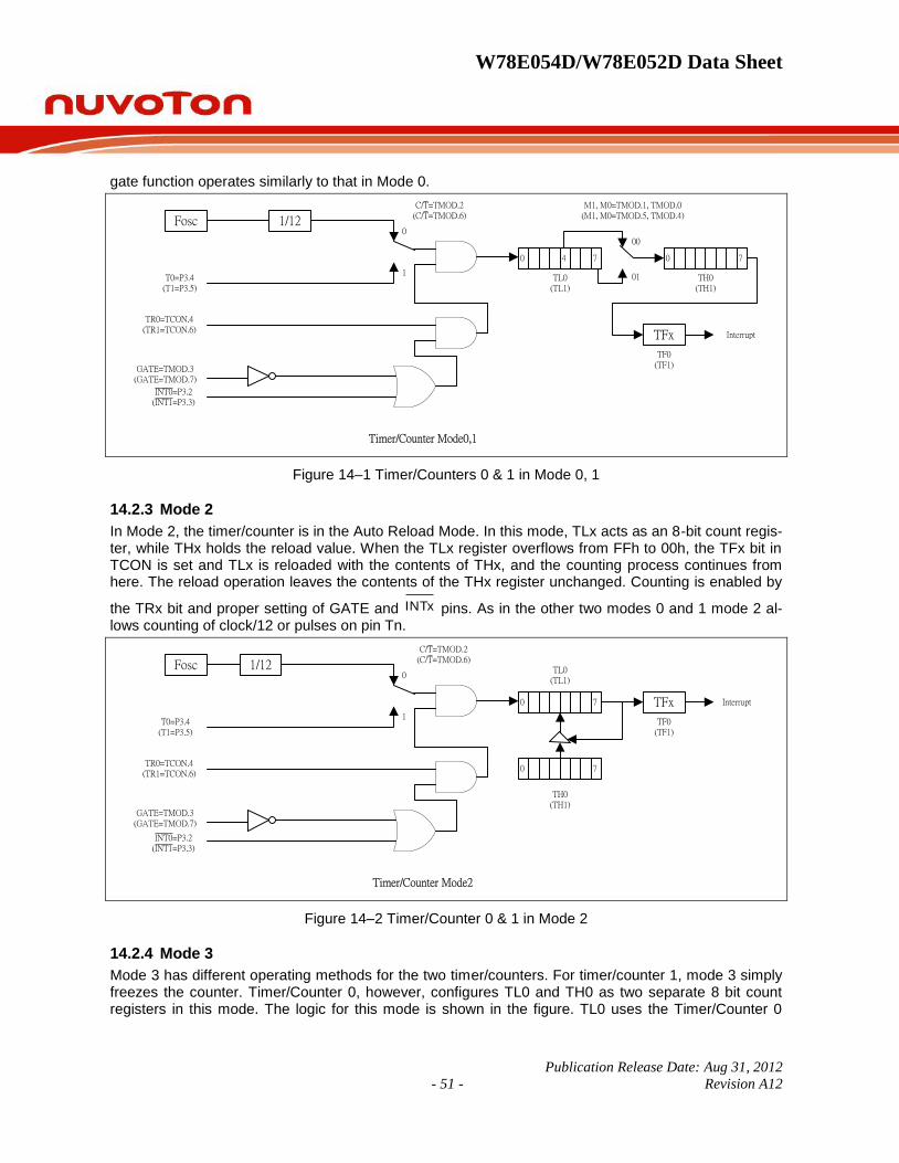
W78E054D/W78E052D Data Sheet
Publication Release Date: Aug 31, 2012
- 51 - Revision A12
gate function operates similarly to that in Mode 0.
1/12Fosc
T0=P3.4(T1=P3.5)
0
1
TR0=TCON.4(TR1=TCON.6)
GATE=TMOD.3(GATE=TMOD.7)
INT0=P3.2(INT1=P3.3)
C/T=TMOD.2(C/T=TMOD.6)
0 7 0 7
TFx Interrupt
TL0(TL1)
TH0(TH1)
TF0(TF1)
Timer/Counter Mode0,1
4
M1, M0=TMOD.1, TMOD.0(M1, M0=TMOD.5, TMOD.4)
00
01
Figure 14–1 Timer/Counters 0 & 1 in Mode 0, 1
14.2.3 Mode 2
In Mode 2, the timer/counter is in the Auto Reload Mode. In this mode, TLx acts as an 8-bit count regis-ter, while THx holds the reload value. When the TLx register overflows from FFh to 00h, the TFx bit in TCON is set and TLx is reloaded with the contents of THx, and the counting process continues from here. The reload operation leaves the contents of the THx register unchanged. Counting is enabled by
the TRx bit and proper setting of GATE and INTx pins. As in the other two modes 0 and 1 mode 2 al-lows counting of clock/12 or pulses on pin Tn.
1/12Fosc
T0=P3.4(T1=P3.5)
0
1
TR0=TCON.4(TR1=TCON.6)
GATE=TMOD.3(GATE=TMOD.7)
INT0=P3.2(INT1=P3.3)
C/T=TMOD.2(C/T=TMOD.6)
0 7
0 7
TFx Interrupt
TL0(TL1)
TH0(TH1)
TF0(TF1)
Timer/Counter Mode2
Figure 14–2 Timer/Counter 0 & 1 in Mode 2
14.2.4 Mode 3
Mode 3 has different operating methods for the two timer/counters. For timer/counter 1, mode 3 simply freezes the counter. Timer/Counter 0, however, configures TL0 and TH0 as two separate 8 bit count registers in this mode. The logic for this mode is shown in the figure. TL0 uses the Timer/Counter 0

W78E054D/W78E052D Data Sheet
- 52 -
control bits TC/ , GATE, TR0, INT0 and TF0. The TL0 can be used to count clock cycles (clock/12) or 1-to-0 transitions on pin T0 as determined by C/T (TMOD.2). TH0 is forced as a clock cycle counter (clock/12) and takes over the use of TR1 and TF1 from Timer/Counter 1. Mode 3 is used in cases where an extra 8 bit timer is needed. With Timer 0 in Mode 3, Timer 1 can still be used in Modes 0, 1 and 2, but its flexibility is somewhat limited. While its basic functionality is maintained, it no longer has control over its overflow flag TF1 and the enable bit TR1. Timer 1 can still be used as a timer/counter and retains the use of GATE and INT1 pin. In this condition it can be turned on and off by switching it out of and into its own Mode 3. It can also be used as a baud rate generator for the serial port.
1/12Fosc
T0=P3.4
0
1
TR0=TCON.4
GATE=TMOD.3
INT0=P3.2
C/T=TMOD.2
0 7
0 7
TF0 Interrupt
TL0
TH0
TR1=TCON.6TF1 Interrupt
Figure 14–3 Timer/Counter Mode 3
14.3 Timer/Counter 2
Timer/Counter 2 is a 16 bit up/down counter which is configured by the T2MOD(bit 0) register and con-trolled by the T2CON register. Timer/Counter 2 is equipped with a capture/reload capability. As with the Timer 0 and Timer 1 counters, there exists considerable flexibility in selecting and controlling the clock, and in defining the operating mode. The clock source for Timer/Counter 2 may be selected for either the external T2 pin (C/T2 = 1) or the crystal oscillator, which is divided by 12 (C/T2 = 0). The clock is then enabled when TR2 is a 1, and disabled when TR2 is a 0.
14.3.1 Capture Mode
The capture mode is enabled by setting the CP RL/ 2 bit in the T2CON register to a 1. In the capture mode, Timer/Counter 2 serves as a 16 bit up counter. When the counter rolls over from 0FFFFh to 0000h, the TF2 bit is set, which will generate an interrupt request. If the EXEN2 bit is set, then a nega-tive transition of T2EX pin will cause the value in the TL2 and TH2 register to be captured by the RCAP2L and RCAP2H registers. This action also causes the EXF2 bit in T2CON to be set, which will also generate an interrupt.

W78E054D/W78E052D Data Sheet
Publication Release Date: Aug 31, 2012
- 53 - Revision A12
(RCLK,TCLK, RL2CP/ )= (0,0,1)
1/12Fosc
T2=P1.0
0
1
T2EX=P1.1
C/T2=T2CON.1
EXF2
Timer2 Interrupt
T2CON.6
TR2=T2CON.2
EXEN2=T2CON.3
TL2 TH2
RCAP2L RCAP2H
TF2
T2CON.7
Figure 14–4 16-Bit Capture Mode
14.3.2 Auto-Reload Mode, Counting up
The auto-reload mode as an up counter is enabled by clearing the CP RL/ 2 bit in the T2CON register and clearing the DCEN bit in T2MOD(bit0) register. In this mode, Timer/Counter 2 is a 16 bit up coun-ter. When the counter rolls over from 0FFFFh, a reload is generated that causes the contents of the RCAP2L and RCAP2H registers to be reloaded into the TL2 and TH2 registers. The reload action also sets the TF2 bit. If the EXEN2 bit is set, then a negative transition of T2EX pin will also cause a reload. This action also sets the EXF2 bit in T2CON.
(RCLK,TCLK, RL2CP/ )= (0,0,0) & DCEN= 0
1/12Fosc
T2=P1.0
0
1
C/T2=T2CON.1
EXF2
Timer2 Interrupt
T2CON.6
TR2=T2CON.2
TL2 TH2
RCAP2L RCAP2H
TF2
T2CON.7
Figure 14–5 16-Bit Auto-reload Mode, Counting Up
14.3.3 Auto-reload Mode, Counting Up/Down
Timer/Counter 2 will be in auto-reload mode as an up/down counter if CP RL/ 2 bit in T2CON is
cleared and the DCEN bit in T2MOD is set. In this mode, Timer/Counter 2 is an up/down counter whose direction is controlled by the T2EX pin. A 1 on this pin cause the counter to count up. An over-flow while counting up will cause the counter to be reloaded with the contents of the capture registers. The next down count following the case where the contents of Timer/Counter equal the capture regis-

W78E054D/W78E052D Data Sheet
- 54 -
ters will load a 0FFFFh into Timer/Counter 2. In either event a reload will set the TF2 bit. A reload will also toggle the EXF2 bit. However, the EXF2 bit cannot generate an interrupt while in this mode.
(RCLK,TCLK, RL2CP/ )= (0,0,0) & DCEN= 1
1/12Fosc
T2=P1.0
0
1
T2EX=P1.1
C/T2=T2CON.1
EXF2
Timer2 Interrupt
T2CON.6
TR2=T2CON.2
TL2 TH2
RCAP2L RCAP2H
TF2
T2CON.7
0FFh 0FFh
Down Counting Reload Value
Up Counting Reload Value
Figure 14–6 16-Bit Auto-reload Mode, Counting Up
14.3.4 Baud Rate Generator Mode
The baud rate generator mode is enabled by setting either the RCLK or TCLK bits in T2CON register. While in the baud rate generator mode, Timer/Counter 2 is a 16 bit counter with auto reload when the count rolls over from 0FFFFh. However, rolling over does not set the TF2 bit. If EXEN2 bit is set, then a negative transition of the T2EX pin will set EXF2 bit in the T2CON register and cause an interrupt re-quest.
RCLK+TCLK=1, RL2CP/ =0
Fosc
T2=P1.0
0
1
T2EX=P1.1
C/T2=T2CON.1
EXF2 Timer2 Interrupt
T2CON.6
TR2=T2CON.2
EXEN2=T2CON.3
TL2 TH2
RCAP2L RCAP2H
1/16
1/16
1
1
0
0
RCLK=T2CON.5
TCLK=T2CON.4
1/2
0 1
Timer1Overflow
SMOD=PCON.7
Rx Clock
Tx Clock
Timer2Overflow
1/2
Figure 14–7 Baud Rate Generator Mode

W78E054D/W78E052D Data Sheet
Publication Release Date: Aug 31, 2012
- 55 - Revision A12
15 WATCHDOG TIMER
The Watchdog timer is a free-running timer which can be programmed by the user to serve as a system monitor, a time-base generator or an event timer. It is basically a set of dividers that divide the system clock. The divider output is selectable and determines the time-out interval. When the time-out occurs a system reset can also be caused if it is enabled. The main use of the Watchdog timer is as a system monitor. This is important in real-time control applications. In case of power glitches or electro-magnetic interference, the processor may begin to execute errant code. If this is left unchecked the entire system may crash. The watchdog time-out selection will result in different time-out values depending on the clock speed. The Watchdog timer will de disabled on reset. In general, software should restart the Watchdog timer to put it into a known state. The control bits that support the Watchdog timer are dis-cussed below.
ENW : Enable watchdog if set.
CLRW : Clear watchdog timer and Pre-scalar if set. This flag will be cleared automatically
WIDL : If this bit is set, watch-dog is enabled under IDLE mode. If cleared, watchdog is disabled under IDLE mode. Default is cleared.
PS2, PS1, PS0: Watchdog Pre-scalar timer select. Pre-scalar is selected when set PS20 as follows:
PS2 PS1 PS0 Pre-scalar select
0 0 0 2
0 0 1 8
0 1 0 4
0 1 1 16
1 0 0 32
1 0 1 64
1 1 0 128
1 1 1 256
The time-out period is obtained using the following equation for 12T per machine cycle:
msscalareOSC
121000Pr21 14
Before Watchdog time-out occurs, the program must clear the 14-bit timer by writing 1 to WDTC.6 (CLRW). After 1 is written to this bit, the 14-bit timer, Pre-scalar and this bit will be reset on the next instruction cycle. The Watchdog timer is cleared on reset.

W78E054D/W78E052D Data Sheet
- 56 -
OSC1/12
1/6Pre-Scalar
14- BIT TIMERCLEAR
CLRW
EXTERNAL
RESET
INTERNAL
RESET
WIDL
IDLE
ENW
Figure 15–1 Watchdog Timer Block Diagram
Typical Watch-Dog time-out period when OSC = 20 MHz
PS2 PS1 PS0 Watchdog time-out period
(for 12T per machine cycle)
0 0 0 19.66 mS
0 1 0 78.64 mS
0 0 1 39.32 mS
0 1 1 157.28 mS
1 0 0 314.57 mS
1 0 1 629.14 mS
1 1 0 1.25 S
1 1 1 2.50 S
Table 15–2 Watch-Dog time-out period for 12T per machine cycle, 20MHz
PS2 PS1 PS0 Watchdog time-out period
(for 6T per machine cycle)
0 0 0 9.83 mS
0 1 0 39.32 mS
0 0 1 19.66 mS
0 1 1 78.64 mS
1 0 0 157.28 mS
1 0 1 314.57mS
1 1 0 629.14 mS
1 1 1 1.250 S
Table 15–3 Watch-Dog time-out period for 6T per machine cycle, 20MHz

W78E054D/W78E052D Data Sheet
Publication Release Date: Aug 31, 2012
- 57 - Revision A12
16 SERIAL PORT
Serial port in this device is a full duplex port. The serial port is capable of synchronous as well as asyn-chronous communication. In Synchronous mode the device generates the clock and operates in a half-duplex mode. In the asynchronous mode, full duplex operation is available. This means that it can sim-ultaneously transmit and receive data. The transmit register and the receive buffer are both addressed as SBUF Special Function Register. However any write to SBUF will be to the transmit register, while a read from SBUF will be from the receiver buffer register. The serial port can operate in four different modes as described below.
16.1 MODE 0
This mode provides synchronous communication with external devices. In this mode serial data is transmitted and received on the RXD line. TXD is used to transmit the shift clock. The TxD clock is pro-vided by the device whether it is transmitting or receiving. This mode is therefore a half-duplex mode of serial communication. In this mode, 8 bits are transmitted or received per frame. The LSB is transmit-ted/received first. The baud rate is fixed at 1/12 of the oscillator frequency. This Baud Rate is deter-mined by the SM2 bit (SCON.5). When this bit is set to 0, then the serial port runs at 1/12 of the clock. This additional facility of programmable baud rate in mode 0 is the only difference between the stand-ard 8051 and W78E054D/W78E052D.
The functional block diagram is shown below. Data enters and leaves the Serial port on the RxD line. The TxD line is used to output the shift clock. The shift clock is used to shift data into and out of this device and the device at the other end of the line. Any instruction that causes a write to SBUF will start the transmission. The shift clock will be activated and data will be shifted out on the RxD pin till all 8 bits are transmitted. If SM2 = 1, then the data on RxD will appear 1 clock period before the falling edge of shift clock on TxD. The clock on TxD then remains low for 2 clock periods, and then goes high again. If SM2 = 0, the data on RxD will appear 3 clock periods before the falling edge of shift clock on TxD. The clock on TxD then remains low for 6 clock periods, and then goes high again. This ensures that at the receiving end the data on RxD line can either be clocked on the rising edge of the shift clock on TxD or latched when the TxD clock is low.

W78E054D/W78E052D Data Sheet
- 58 -
1/12
Fosc
0 TX CLOCK
RX CLOCK
TI
RI
TX SHIFT
TX STARTRX SHIFT
LOAD SBUF
SHIFT CLOCK
RIREN
SM2
CLOCK
SINPAROUT SBUF
Read SBUF
Internal
Data Bus
Serial Controllor
CLOCK
LOAD
PARIN
TX START
Internal
Data Bus
Write to
SBUF
SOUT
Transmit Shift Register
Serial Interrupt
RXD
TXD
RXDP3.0 Alternate
Input Function
P3.0 Alternate
Output Function
P3.1 Alternate
Output Function
1/4
1
Receive Shift Register
Figure 16–1 Serial port mode 0
The TI flag is set high in S6P2 following the end of transmission of the last bit. The serial port will re-ceive data when REN is 1 and RI is zero. The shift clock (TxD) will be activated and the serial port will latch data on the rising edge of shift clock. The external device should therefore present data on the falling edge on the shift clock. This process continues till all the 8 bits have been received. The RI flag is set in S6P2 following the last rising edge of the shift clock on TxD. This will stop reception, till the RI is cleared by software.
16.2 MODE 1
In Mode 1, the full duplex asynchronous mode is used. Serial communication frames are made up of 10 bits transmitted on TXD and received on RXD. The 10 bits consist of a start bit (0), 8 data bits (LSB first), and a stop bit (1). On receive, the stop bit goes into RB8 in the SFR SCON. The baud rate in this mode is variable. The serial baud can be programmed to be 1/16 or 1/32 of the Timer 1 overflow. Since the Timer 1 can be set to different reload values, a wide variation in baud rates is possible.
Transmission begins with a write to SBUF. The serial data is brought out on to TxD pin at S6P2 follow-ing the first roll-over of divide by 16 counter. The next bit is placed on TxD pin at S6P2 following the next rollover of the divide by 16 counter. Thus the transmission is synchronized to the divide by 16 counter and not directly to the write to SBUF signal. After all 8 bits of data are transmitted, the stop bit is transmitted. The TI flag is set in the S6P2 state after the stop bit has been put out on TxD pin. This will be at the 10th rollover of the divide by 16 counters after a write to SBUF.
Reception is enabled only if REN is high. The serial port actually starts the receiving of serial data, with the detection of a falling edge on the RxD pin. The 1-to-0 detector continuously monitors the RxD line, sampling it at the rate of 16 times the selected baud rate. When a falling edge is detected, the divide by 16 counters is immediately reset. This helps to align the bit boundaries with the rollovers of the divide by 16 counters.

W78E054D/W78E052D Data Sheet
Publication Release Date: Aug 31, 2012
- 59 - Revision A12
The 16 states of the counter effectively divide the bit time into 16 slices. The bit detection is done on a best of three basis. The bit detector samples the RxD pin, at the 8th, 9th and 10th counter states. By using a majority 2 of 3 voting system, the bit value is selected. This is done to improve the noise rejec-tion feature of the serial port. If the first bit detected after the falling edge of RxD pin is not 0, then this indicates an invalid start bit, and the reception is immediately aborted. The serial port again looks for a falling edge in the RxD line. If a valid start bit is detected, then the rest of the bits are also detected and shifted into the SBUF.
After shifting in 8 data bits, there is one more shift to do, after which the SBUF and RB8 are loaded and RI is set. However certain conditions must be met before the loading and setting of RI can be done.
1. RI must be 0 and
2. Either SM2 = 0, or the received stop bit = 1.
If these conditions are met, then the stop bit goes to RB8, the 8 data bits go into SBUF and RI is set. Otherwise the received frame may be lost. After the middle of the stop bit, the receiver goes back to looking for a 1-to-0 transition on the RxD pin.
1/2
1/16 TX CLOCK
RX CLOCK
TI
RI
TX SHIFT
TX STARTRX SHIFT
LOAD SBUF
SMOD
CLOCK
SIN D8
SBUF
Read SBUF
Internal
Data Bus
Serial
Controllor
CLOCK
LOAD
PARIN
TX START
Internal
Data BusWrite to
SBUFSOUT
Transmit Shift Register
Serial Interrupt
TXD
RXD
PAROUT
RB8
START
STOP
0
1
BIT
DETECTOR
1-To-0
DETECTOR
SAMPLE
1/16
0
Timer 1
Overflow
1
Receive Shift Register
0 1
0 1
TCLK
RCLK
Timer 2
Overflow
Figure 16–2 Serial port mode 1
16.3 MODE 2
This mode uses a total of 11 bits in asynchronous full-duplex communication. The functional description is shown in the figure below. The frame consists of one start bit (0), 8 data bits (LSB first), a program-mable 9th bit (TB8) and a stop bit (1). The 9th bit received is put into RB8. The baud rate is program-mable to 1/32 or 1/64 of the oscillator frequency, which is determined by the SMOD bit in PCON SFR.

W78E054D/W78E052D Data Sheet
- 60 -
Transmission begins with a write to SBUF. The serial data is brought out on to TxD pin at S6P2 follow-ing the first roll-over of the divide by 16 counter. The next bit is placed on TxD pin at S6P2 following the next rollover of the divide by 16 counter. Thus the transmission is synchronized to the divide by 16 counters, and not directly to the write to SBUF signal. After all 9 bits of data are transmitted, the stop bit is transmitted. The TI flag is set in the S6P2 state after the stop bit has been put out on TxD pin. This will be at the 11th rollover of the divide by 16 counters after a write to SBUF. Reception is enabled only if REN is high. The serial port actually starts the receiving of serial data, with the detection of a falling edge on the RxD pin. The 1-to-0 detector continuously monitors the RxD line, sampling it at the rate of 16 times the selected baud rate. When a falling edge is detected, the divide by 16 counters is immedi-ately reset. This helps to align the bit boundaries with the rollovers of the divide by 16 counters. The 16 states of the counter effectively divide the bit time into 16 slices. The bit detection is done on a best of three basis. The bit detector samples the RxD pin, at the 8th, 9th and 10th counter states. By using a majority 2 of 3 voting system, the bit value is selected. This is done to improve the noise rejection fea-ture of the serial port.
1/2
1/16 TX CLOCK
RX CLOCK
TI
RI
TX SHIFT
TX STARTRX SHIFT
LOAD SBUF
SMOD
CLOCK
SIN D8
SBUF
Read SBUF
Internal
Data Bus
Serial
Controllor
CLOCK
LOAD
PARIN
TX START
Internal
Data BusWrite to
SBUFSOUT
Transmit Shift Register
Serial Interrupt
TXD
RXD
PAROUT
RB8
START
STOP
0
1
BIT
DETECTOR
1-To-0
DETECTOR
SAMPLE
1/16
0
Fosc/2
1
D8TB8
Receive Shift Register
Figure 16–3 Serial port mode 2
If the first bit detected after the falling edge of RxD pin, is not 0, then this indicates an invalid start bit, and the reception is immediately aborted. The serial port again looks for a falling edge in the RxD line. If a valid start bit is detected, then the rest of the bits are also detected and shifted into the SBUF. After shifting in 9 data bits, there is one more shift to do, after which the SBUF and RB8 are loaded and RI is set. However certain conditions must be met before the loading and setting of RI can be done.
1. RI must be 0 and
2. Either SM2 = 0, or the received stop bit = 1.

W78E054D/W78E052D Data Sheet
Publication Release Date: Aug 31, 2012
- 61 - Revision A12
If these conditions are met, then the stop bit goes to RB8, the 8 data bits go into SBUF and RI is set. Otherwise the received frame may be lost. After the middle of the stop bit, the receiver goes back to looking for a 1-to-0 transition on the RxD pin.
MODE 3
This mode is similar to Mode 2 in all respects, except that the baud rate is programmable. The user must first initialize the Serial related SFR SCON before any communication can take place. This in-volves selection of the Mode and baud rate. The Timer 1 should also be initialized if modes 1 and 3 are used. In all four modes, transmission is started by any instruction that uses SBUF as a destination reg-ister. Reception is initiated in Mode 0 by the condition RI = 0 and REN = 1. This will generate a clock on the TxD pin and shift in 8 bits on the RxD pin. Reception is initiated in the other modes by the incoming start bit if REN = 1. The external device will start the communication by transmitting the start bit.
TX CLOCK
RX CLOCK
TI
RI
TX SHIFT
TX STARTRX SHIFT
LOAD SBUF
CLOCK
SIN D8
SBUF
Read SBUF
Internal
Data Bus
Serial
Controllor
CLOCK
LOAD
PARIN
TX START
Internal
Data BusWrite to
SBUF SOUT
Transmit Shift Register
Serial Interrupt
TXD
RXD
PAROUT
RB8
START
STOP
0
1
BIT
DETECTOR
1-To-0
DETECTOR
D8TB8
Receive Shift Register
1/2
1/16
SMOD
SAMPLE
1/16
0
Timer 1
Overflow
1
0 1
0 1
TCLK
RCLK
Timer 2
Overflow
Figure 16–4 Serial port mode 3
SM0 SM1 Mode Type Baud Clock Frame Size
Start Bit
Stop Bit
9th bit Function
0 0 0 Synch. 4 or 12 TCLKS 8 bits No No None
0 1 1 Asynch. Timer 1 or 2 10 bits 1 1 None
1 0 2 Asynch. 32 or 64 TCLKS
11 bits 1 1 0, 1
1 1 3 Asynch. Timer 1 or 2 11 bits 1 1 0, 1
Table 16–5 Serial Ports Modes

W78E054D/W78E052D Data Sheet
- 62 -
17 FLASH ROM CODE BOOT MODE SLECTION
The W78E054D/W78E052D boots from APROM program (16K/8K bytes) or LDROM program (2K bytes) at power on reset or external reset.
BOOT MODE Select by CONFIG bits
CBS (CONFIG.2)
Config boot select at Power-on reset and external reset.
1: Boot from APROM (0x0000).
0: Boot from LDROM (0x3800).

W78E054D/W78E052D Data Sheet
Publication Release Date: Aug 31, 2012
- 63 - Revision A12
18 ISP (IN-SYSTEM PROGRAMMING)
ISP is the ability of program MCU to be programmed while F/W code in AP-ROM or LD-ROM. (Note: Timer 0 for program, erase, read on ISP mode. ISP operation voltage 3.3- 5.5V)
START
Setting control registers
MOV SFRCN,#3Fh
MOV SFRFD,#ABh
MOV SFRAL,#FFh
MOV SFRAH,#FFh
MOV CHPCON,#03h
Setting Timer (about 450 us)
and enable timer interrupt
Start Timer and enter idle Mode.
(CPU will be wakened from idle mode
by timer interrupt, then enter In-System
Programming mode)
Part 1:2KB APROM
procedure of entering
In-System Programming Mode
Execute the normal
Application program
Enter In-System
Programming Mode ?
(conditions depend on
user's application)
END
YES
GO
NO

W78E054D/W78E052D Data Sheet
- 64 -
GO
Timer Interrupt Service Routine:
Stop Timer & disable interrupt
End of Programming
End of erase
operation. CPU will
be wakened by Timer
interrupt.
Setting Timer and enable Timer
interrupt for wake-up .
(15 ms for erasing operation)
Start Timer and enter IDLE
Mode.
(Erasing...)
Part 2:
Procedure of Updating
the 2KB APROM
Is F02K BOOT Mode?
Setting erase operation mode:
MOV ERPAGE,#02H
MOV SFRCN,#22H
(Erase 2KB APROM ISP )
PGM
NO
YES

W78E054D/W78E052D Data Sheet
Publication Release Date: Aug 31, 2012
- 65 - Revision A12
PGM
Read_Device_ID
MOV SFRCN,#0Ch
MOV CHPCON,#03h
Setting Timer and enable Timer
interrupt for wake-up .
(50us for program operation)
Read_VT
MOV SFRCN,#0Dh
MOV SFRAL,#01h
MOV SFRAH,#00h
MOV CHPCON,#03h
.
Part 2:
Procedure of Updating
the 2KB APROM
End of Programming ?
Get the parameters of new code
(Address and data bytes)
through I/O ports, UART or
other interfaces.
Setting control registers for
programming:MOV SFRAH,#ADDRESS_H
MOV SFRAL,#ADDRESS_L
MOV SFRFD,#DATA
MOV SFRCN,#21H
NO
YES Read_Compay_ID
OV SFRCN,#0Bh
MOV CHPCON,#03h
Read_Dist
MOV SFRCN,#0Eh
MOV SFRAL,#02h
MOV SFRAH,#00h
MOV CHPCON,#03h
.
Is currently in the
F02K BOOT Mode ?Ease 14K AP programming:
MOV ERPAGE,#01
MOV SFRCN,#22H

W78E054D/W78E052D Data Sheet
- 66 -
PGM
Software reset CPU and
re-boot from the 2KB
APROM.MOV CHPCON,#81h
Hardware Reset
to re-boot from
new 2 KB APROM.
(S/W reset is
invalid in F02K BOOT
Mode)
Setting Timer and enable Timer
interrupt for wake-up .
(50us for program operation)
END
Executing new code
from address
00H in the 2KB APROM.
Part 2:
Procedure of Updating
the 2KB APROM
End of Programming ?
Get the parameters of new code
(Address and data bytes)
through I/O ports, UART or
other interfaces.
Setting control registers for
programming:
MOV SFRAH,#ADDRESS_H
MOV SFRAL,#ADDRESS_L
MOV SFRFD,#DATA
MOV SFRCN,#21H
Is currently in the
F02K BOOT Mode ?
NO
YES
NO
YESRead_Compay_ID
Read_Device_ID
Read_VT
Read_Dist
Ease 14K AP programming:
MOV ERPAGE,#01
MOV SFRCN,#22H
W78E054D/W78E052D Data Sheet
Publication Release Date: Aug 31, 2012
- 67 - Revision A12
19 CONFIG BITS
During the on-chip Flash EPROM operation mode, the Flash EPROM can be programmed and verified repeatedly. Until the code inside the Flash EPROM is confirmed OK, the code can be protected. The protection of Flash EPROM and those operations on it are described below.
The W78E054D/W78E052D has a Special Setting Register, the config Bits, which cannot be accessed in normal mode. The Security register can only be accessed from the Flash EPROM operation mode. Those bits of the Security Registers cannot be changed once they have been programmed from high to low. They can only be reset through erase-all operation. The Security Register is addressed in the Flash EPROM operation mode by address #0FFFFh.
Special Setting Register
Config Bits16/8/4KB
Flash EPROM
Program Memory
Reserved
Security Register FFFFh
0000h
3FFFh
B0: Lock bit,
logic 0 : active Lock Flash
logic 1 : no Lock Flash.
B1: MOVC inhibit,
logic 0 : the MOVC instruction in external memory
cannot access the code in internal memory
logic 1 : no restriction.
B2: CBS
logic 0: Boot from LD block (0x3800).
logic 1: Boot from AP block (default).
B3: NSR ( Noise Sensitivity Reduction)
logic 0: Noise Sensitivity Reduction is enabled.
logic 1: Noise Sensitivity Reduction is disabled.
B5: Machine Cycle Select
logic 0 : 6T
logic 1 : 12T
B7: Crystal Select
logic 0 : 1/2 gain, 24MHz
logic 1 : Full gain, 40MHz
Default 1 for all security bits.
Reserved bits must be kept in logic 1.
B0B1B2B3B4B5B6B7

W78E054D/W78E052D Data Sheet
- 68 -
Bit 0: Lock bits
0: Lock enable
1: Lock disable
This bit is used to protect the customer's program code in the W78E054D/W78E052D. It may be set after the programmer finishes the programming and verifies sequence. Once these bits are set to logic 0, both the FLASH data and Special Setting Registers cannot be accessed again.
Bit 1: MOVC inhibit
0: MOVC inhibit enable
1: MOVC inhibit disable
This bit is used to restrict the accessible region of the MOVC instruction. It can prevent the MOVC in-struction in external program memory from reading the internal program code. When this bit is set to logic 0, a MOVC instruction in external program memory space will be able to access code only in the external memory, not in the internal memory. A MOVC instruction in internal program memory space will always be able to access the ROM data in both internal and external memory. If this bit is logic 1, there are no restrictions on the MOVC instruction.
Bit 2: CBS
Config boot select at Power-on reset and external reset.
CBS=1: Boot from APROM block (default).
CBS=0: Boot from LDROM block (0x3800).
Bit 3: NSR (Noise Sensitivity Reduction) NSR=1: Noise Sensitivity Reduction is disabled. NSR=0: Noise Sensitivity Reduction is enabled.
Bit 4: Must be “1”
Bit 5: Machine Cycle Select
This bit is select MCU core, default value is logic 1, and the MCU core is 12T per instruction. Once this bit is set to logic 0, the MCU core is 6T per instruction.
Bit 6: Must be “1”
Bit 7: Crystal Select
0 (24MHz): If system clock is slower than 24MHz, programming “0”. It can reduce EMI effect and save the power consumption.
1 (40MHz): If system clock is faster than 24MHz, programming “1”.

W78E054D/W78E052D Data Sheet
Publication Release Date: Aug 31, 2012
- 69 - Revision A12
20 ELECTRICAL CHARACTERISTICS
20.1 Absolute Maximum Ratings
SYMBOL PARAMETER Min MAX UNIT
DC Power Supply VDDVSS 2.4 5.5 V
Input Voltage VIN VSS-0.3 VDD+0.3 V
Operating Temperature
(W78E054D/W78E052D)
TA -40 +85 C
Note: Exposure to conditions beyond those listed under absolute maximum ratings may adversely af-fects the lift and reliability of the device.

W78E054D/W78E052D Data Sheet
- 70 -
20.2 DC ELECTRICAL CHARACTERISTICS
TA =-40℃~+85℃, VDD=2.4V~5.5V, VSS=0V
Sym Parameter Test Condition Min Typ*1
Max Unit
VIL
Input Low Voltage
(Ports 0~4, /EA, XTAL1, RST)
2.4 < VDD < 5.5V -0.5 0.2VDD
-0.1 V
VIH Input High Voltage
(Ports 0~4, /EA) 2.4 < VDD < 5.5V
0.2VDD
+0.9
VDD+
0.5 V
VIH1 Input High Voltage
(XTAL1, RST) 2.4 < VDD < 5.5V 0.7VDD
VDD+
0.5 V
VOL
Output Low Voltage
(Ports 0~4, ALE, /PSEN)
VDD=4.5V, IOL= 12.0mA*3,*4
VDD=2.4V, IOL= 10mA*3,*4
0.4 V
VOH1 Output High Voltage
(Ports 1~4)
VDD=4.5V, IOH= -300A*4
VDD=2.4V, IOH= -35A*4
2.4
2.0 V
VOH2
Output High Voltage
(Ports 0 & 2 in external bus mode, ALE, /PSEN)
VDD=4.5V, IOH= -8.0mA*4
VDD=2.4V, IOH= -2.2mA*4
2.4
2.0 V
I IL Logical 0 Input Current
(Ports 1~4) VDD=5.5V, VIN=0.4V -45 -50 A
ITL Logical 1-to-0 Transition
Current (Ports 1~4) *2
VDD=5.5V, VIN=2.0V -510 -650 A
I LI Input Leakage Current
(Port 0) 0 < VIN < VDD+0.5 ±0.1 ±10 A
I DD Power Supply Current
Active mode*5
@12MHz, VDD=5.0V
@40MHz, VDD=5.0V
@12MHz, VDD=3.3V
@20MHz, VDD=3.3V
9.5
16.0
3.1
3.7
mA
Idle mode
@12MHz, VDD=5.0V
@40MHz, VDD=5.0V
@12MHz, VDD=3.3V
@20MHz, VDD=3.3V
3.5
9.2
1.2
1.7
mA
Power-down mode <1 50 A
RRST RST-pin Internal Pull-down Resistor
2.4 < VDD < 5.5V 100 225 KΩ
Note:
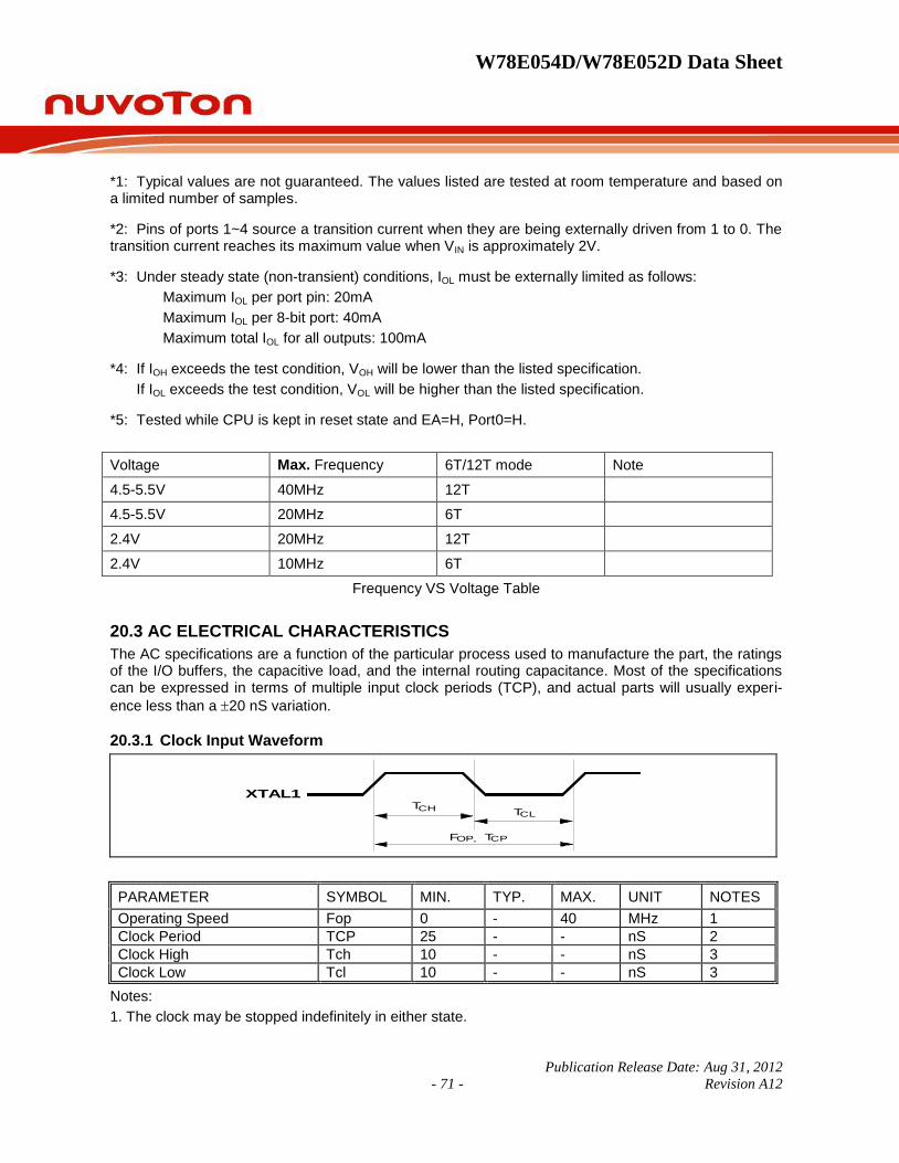
W78E054D/W78E052D Data Sheet
Publication Release Date: Aug 31, 2012
- 71 - Revision A12
*1: Typical values are not guaranteed. The values listed are tested at room temperature and based on a limited number of samples.
*2: Pins of ports 1~4 source a transition current when they are being externally driven from 1 to 0. The transition current reaches its maximum value when VIN is approximately 2V.
*3: Under steady state (non-transient) conditions, IOL must be externally limited as follows:
Maximum IOL per port pin: 20mA
Maximum IOL per 8-bit port: 40mA
Maximum total IOL for all outputs: 100mA
*4: If IOH exceeds the test condition, VOH will be lower than the listed specification.
If IOL exceeds the test condition, VOL will be higher than the listed specification.
*5: Tested while CPU is kept in reset state and EA=H, Port0=H.
Voltage Max. Frequency 6T/12T mode Note
4.5-5.5V 40MHz 12T
4.5-5.5V 20MHz 6T
2.4V 20MHz 12T
2.4V 10MHz 6T
Frequency VS Voltage Table
20.3 AC ELECTRICAL CHARACTERISTICS
The AC specifications are a function of the particular process used to manufacture the part, the ratings of the I/O buffers, the capacitive load, and the internal routing capacitance. Most of the specifications can be expressed in terms of multiple input clock periods (TCP), and actual parts will usually experi-
ence less than a 20 nS variation.
20.3.1 Clock Input Waveform
TT
XTAL1
F
CHCL
OP, TCP
PARAMETER SYMBOL MIN. TYP. MAX. UNIT NOTES
Operating Speed Fop 0 - 40 MHz 1
Clock Period TCP 25 - - nS 2
Clock High Tch 10 - - nS 3
Clock Low Tcl 10 - - nS 3
Notes:
1. The clock may be stopped indefinitely in either state.

W78E054D/W78E052D Data Sheet
- 72 -
2. The TCP specification is used as a reference in other specifications.
3. There are no duty cycle requirements on the XTAL1 input.
20.3.2 Program Fetch Cycle
PARAMETER SYMBOL MIN. TYP. MAX. UNIT NOTES
Address Valid to ALE Low Taas 1 TCP -
- - nS 4
Address Hold from ALE Low Taah 1 TCP -
- - nS 1, 4
ALE Low to PSEN Low Tapl 1 TCP -
- - nS 4
PSEN Low to Data Valid Tpda - - 2 TCP nS 2
Data Hold after PSEN High Tpdh 0 - 1 TCP nS 3
Data Float after PSEN High Tpdz 0 - 1 TCP nS
ALE Pulse Width Talw 2 TCP -
2 TCP - nS 4
PSEN Pulse Width Tpsw 3 TCP -
3 TCP - nS 4
Notes:
1. P0.0P0.7, P2.0P2.7 remains stable throughout entire memory cycle.
2. Memory access time is 3 TCP.
3. Data have been latched internally prior to PSEN going high.
4. "" (due to buffer driving delay and wire loading) is 20 nS.
20.3.3 Data Read Cycle
PARAMETER SYMBOL MIN. TYP. MAX. UNIT NOTES
ALE Low to RD Low Tdar 3 TCP - - 3 TCP + nS 1, 2
RD Low to Data Valid Tdda - - 4 TCP nS 1
Data Hold from RD High Tddh 0 - 2 TCP nS
Data Float from RD High Tddz 0 - 2 TCP nS
RD Pulse Width Tdrd 6 TCP - 6 TCP - nS 2
Notes:
1. Data memory access time is 8 TCP.
2. "" (due to buffer driving delay and wire loading) is 20 nS.

W78E054D/W78E052D Data Sheet
Publication Release Date: Aug 31, 2012
- 73 - Revision A12
20.3.4 Data Write Cycle
PARAMETER SYMBOL MIN. TYP. MAX. UNIT
ALE Low to WR Low Tdaw 3 TCP - - 3 TCP + nS
Data Valid to WR Low Tdad 1 TCP - - - nS
Data Hold from WR High Tdwd 1 TCP - - - nS
WR Pulse Width Tdwr 6 TCP - 6 TCP - nS
Note: "" (due to buffer driving delay and wire loading) is 20 nS.
20.3.5 Port Access Cycle
PARAMETER SYMBOL MIN. TYP. MAX. UNIT
Port Input Setup to ALE Low Tpds 1 TCP - - nS
Port Input Hold from ALE Low Tpdh 0 - - nS
Port Output to ALE Tpda 1 TCP - - nS
Note: Ports are read during S5P2, and output data becomes available at the end of S6P2. The timing data are referenced to ALE, since it provides a convenient reference.

W78E054D/W78E052D Data Sheet
- 74 -
20.4 TIMING waveforms
20.4.1 Program Fetch Cycle
S1
XTAL1
S2 S3 S4 S5 S6 S1 S2 S3 S4 S5 S6
ALE
PORT 2
A0-A7A0-A7 DataA0-A7 Code
T
A0-A7 DataCode
PORT 0
PSEN
PDH, TPDZ
TPDATAAH
TAAS
TPSW
TAPL
TALW
20.4.2 Data Read Cycle
S2 S3S5 S6 S1S2 S3 S4S1S5 S6S4
XTAL1
ALE
PSEN
A8-A15
DATA OUT
PORT 2
PORT 0 A0-A7
WRT
TDAW
DAD
TDWR
TDWD

W78E054D/W78E052D Data Sheet
Publication Release Date: Aug 31, 2012
- 75 - Revision A12
20.4.3 Data Write Cycle
S2 S3S5 S6 S1S2 S3 S4S1S5 S6S4
XTAL1
ALE
PSEN
A8-A15
DATA OUT
PORT 2
PORT 0 A0-A7
WRT
TDAW
DAD
TDWR
TDWD
20.4.4 Port Access Cycle
XTAL1
ALE
S5 S6 S1
DATA OUT
TT
PORT
INPUT
T
SAMPLE
PDAPDHPDS

W78E054D/W78E052D Data Sheet
- 76 -
20.4.5 Reset Pin Access Cycle
VSS
VDD
POF
Internal
Reset
Power
1 = reset state
0 = cpu free running
~0.7V
Reset
Pin
ALE
Crystal
Clock
65536 crystal clock
~2.0V
12 Crystal Clock = 1 Machine Cycle
24 crystal clock

W78E054D/W78E052D Data Sheet
Publication Release Date: Aug 31, 2012
- 77 - Revision A12
21 APPLICATION CIRCUITS
21.1 External Program Memory and Crystal
A2
AD4A5
AD0
A5
A9
A3
AD7A7
AD1
A15
A4
AD6
A1AD2
A14
A1 AD1
A3AD3
ALE
R
A10
AD3A4
AD5AD4
C1
A13
A15
AD7
VCC
A0
CRYSTAL
RST
A11
A9
74373
3 24 57 68 9
13 1214 1517 1618 19
111
D0 Q0D1 Q1D2 Q2D3 Q3D4 Q4D5 Q5D6 Q6D7 Q7
OCG
AD4
A6C2
PSEN8.2K
A8
A12
AD0
A2
W78I052DDG-40DIP
A11
A14
AD5
AD2
A7
A12
AD6
AD3
AD6 A6
W78I054DDG-40DIP
31
19
18
9
12131415
12345678
3938373635343332
2122232425262728
1716
29301110
20
40
EA
XTAL1
XTAL2
RST
P3.2/INT0P3.3/INT1P3.4/T0P3.5/T1
P1.0/T2P1.1/T2EXP1.2P1.3P1.4P1.5P1.6P1.7
P0.0P0.1P0.2P0.3P0.4P0.5P0.6P0.7
P2.0P2.1P2.2P2.3P2.4P2.5P2.6P2.7
RD/P3.7WR/P3.6
PSENALE
TXD/P3.1RXD/P3.0
VS
S
VD
D
A10
AD7
AD2
AD5
VCC
A8
A0 AD0AD1
10uF
A13
64KB ROM
109876543
252421232
26271
2022
1112131516171819
A0A1A2A3A4A5A6A7A8A9A10A11A12A13A14A15
CEOE
O0O1O2O3O4O5O6O7
Figure A
21.2 Expanded External Data Memory and Oscillator
AD0 A0
A10
VCC
AD4
AD6
8.2K
AD3
A13
A0
A2
64KB RAM
12111098765
272623254
283
31
1314151718192021
22302429
A0A1A2A3A4A5A6A7A8A9A10A11A12A13A14A15
D0D1D2D3D4D5D6D7
CS1CS2OEWE
AD5
A2
A11
AD1
A15A14
AD4
AD2
A5
AD3
A15
AD4
A12
A4A4
AD2
AD7
AD2
A14
AD6
/WR
VCC
AD5
RST
A1AD0 AD0
/RD
A1
A8
A6A5
VCC
W78I054DDG-40DIP
31
19
18
9
12131415
12345678
3938373635343332
2122232425262728
1716
29301110
20
40
EA
XTAL1
XTAL2
RST
P3.2/INT0P3.3/INT1P3.4/T0P3.5/T1
P1.0/T2P1.1/T2EXP1.2P1.3P1.4P1.5P1.6P1.7
P0.0P0.1P0.2P0.3P0.4P0.5P0.6P0.7
P2.0P2.1P2.2P2.3P2.4P2.5P2.6P2.7
RD/P3.7WR/P3.6
PSENALE
TXD/P3.1RXD/P3.0
VS
S
VD
D
A9
ALE
A9
A13
VCC
OscillatorAD3
AD7
AD5
A3
W78I052DDG-40DIP
A10
AD6
A3
A7
10uF
A12
AD1 AD1
A7
74373
3 24 57 68 9
13 1214 1517 1618 19
111
D0 Q0D1 Q1D2 Q2D3 Q3D4 Q4D5 Q5D6 Q6D7 Q7
OCG
A6
A11
AD7
A8
Figure B
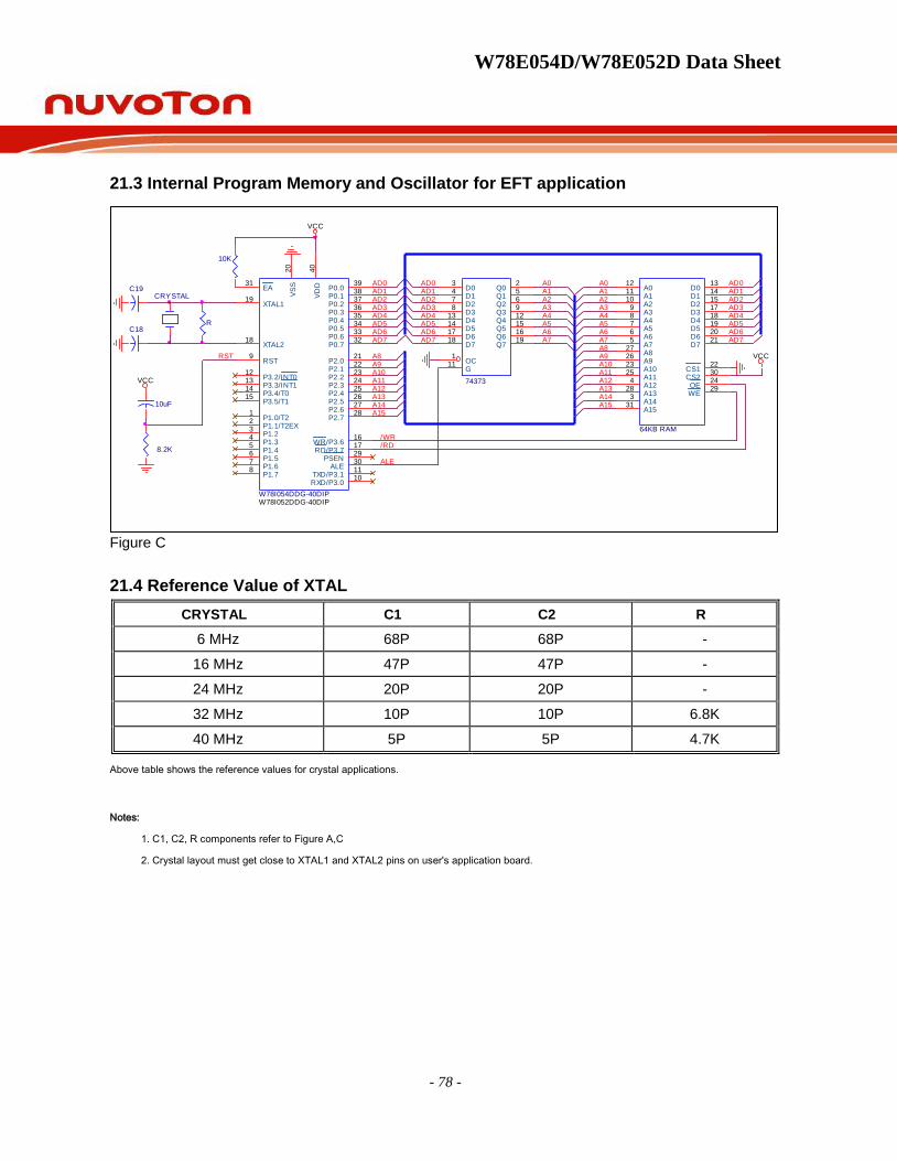
W78E054D/W78E052D Data Sheet
- 78 -
21.3 Internal Program Memory and Oscillator for EFT application
A6AD5
AD6
C19
A8
A3
A12
AD0
A2
AD6
74373
3 24 57 68 9
13 1214 1517 1618 19
111
D0 Q0D1 Q1D2 Q2D3 Q3D4 Q4D5 Q5D6 Q6D7 Q7
OCG
VCC
AD1
AD3 AD3
A10
A2
10K
CRYSTAL
A9A10
AD1
C18
AD4
AD2
VCC
AD5
RST
A13A14
W78I054DDG-40DIP
31
19
18
9
12131415
12345678
3938373635343332
2122232425262728
1716
29301110
20
40
EA
XTAL1
XTAL2
RST
P3.2/INT0P3.3/INT1P3.4/T0P3.5/T1
P1.0/T2P1.1/T2EXP1.2P1.3P1.4P1.5P1.6P1.7
P0.0P0.1P0.2P0.3P0.4P0.5P0.6P0.7
P2.0P2.1P2.2P2.3P2.4P2.5P2.6P2.7
RD/P3.7WR/P3.6
PSENALE
TXD/P3.1RXD/P3.0
VS
S
VD
DA4
AD0A1
AD7
AD0
/WR
A6
A9
A1
A14
/RD
AD6
AD2
A5
A8
A5AD4
8.2K
A15
AD2
AD7
A13A12
A15
R
A11
ALE
VCC
A3
AD5
A0
AD3
10uF
A11
A7
64KB RAM
12111098765
272623254
283
31
1314151718192021
22302429
A0A1A2A3A4A5A6A7A8A9A10A11A12A13A14A15
D0D1D2D3D4D5D6D7
CS1CS2OEWE
W78I052DDG-40DIP
AD4
A0
A4
AD1
A7AD7
Figure C
21.4 Reference Value of XTAL
CRYSTAL C1 C2 R
6 MHz 68P 68P -
16 MHz 47P 47P -
24 MHz 20P 20P -
32 MHz 10P 10P 6.8K
40 MHz 5P 5P 4.7K
Above table shows the reference values for crystal applications.
Notes:
1. C1, C2, R components refer to Figure A,C
2. Crystal layout must get close to XTAL1 and XTAL2 pins on user's application board.

W78E054D/W78E052D Data Sheet
Publication Release Date: Aug 31, 2012
- 79 - Revision A12
22 APPLICATION NOTE
In-system Programming Software Examples
This application note illustrates the in-system programmability of the microcontroller. In this example, microcontroller will boot from 2K LDROM bank enter in-system programming mode for programming the contents of APROM, this sample to Erase APROM, Erase Verify APROM, Read one byte for APROM, Write one byte for APROM, Read CID/DID. .
EXAMPLE: Base on Keil C51 Compiler
$nomod51
#include <reg52.h>
EAPAGE DATA 0BEh
CHPCON DATA 0BFh
SFRAL DATA 0C4h
SFRAH DATA 0C5h
SFRFD DATA 0C6h
SFRCN DATA 0C7h
;CPU Clock = 12MHz/12T mode
READ_TIME EQU 1
PROGRAM_TIME EQU 50
ERASE_TIME EQU 5000
;For W78E(I)054D
APROM_END_ADDRESS EQU 03800h
;For W78E(I)052D
;APROM_END_ADDRESS EQU 02000h
FLASH_STANDBY EQU 00111111B
READ_CID EQU 00001011B
READ_DID EQU 00001100B
ERASE_ROM EQU 00100010B
ERASE_VERIFY EQU 00001001B
PROGRAM_ROM EQU 00100001B
PROGRAM_VERIFY_ROM EQU 00001010B
READ_ROM EQU 00000000B
ORG 03800h

W78E054D/W78E052D Data Sheet
- 80 -
mov SP,#060h
mov TMOD,#01h ;Set Timer0 as mode1
call Read_Company_ID
call Read_Device_ID_HIGH
call Read_Device_ID_LOW
call Erase_APROM
call Erase_Verify_ROM
call Program_APROM
call Program_Verify_APROM
call Software_Reset
sjmp $
;************************************************************************
; * Read_Company_ID
;************************************************************************
Read_Company_ID:
mov SFRCN,#READ_CID
mov TL0,#LOW (65536-READ_TIME)
mov TH0,#HIGH(65536-READ_TIME)
setb TR0
mov CHPCON,#00000011b
clr TF0
clr TR0
mov A,SFRFD ;check Read company ID
cjne A,#0DAh,CID_Error
ret
CID_Error:
mov P1,#01h
sjmp $
;************************************************************************
; * read device ID high
;************************************************************************
Read_Device_ID_HIGH:
mov SFRAL,#0FFh
mov SFRAH,#0FFh
mov SFRCN,#READ_DID
mov TL0,#LOW (65536-READ_TIME)
mov TH0,#HIGH(65536-READ_TIME)
setb TR0
mov CHPCON,#00000011b
clr TF0
clr TR0
mov A,SFRFD ;read device id high byte
ret

W78E054D/W78E052D Data Sheet
Publication Release Date: Aug 31, 2012
- 81 - Revision A12
;*************************************************************************
; * read device ID low
;*************************************************************************
Read_Device_ID_LOW:
mov SFRAL,#0FEh
mov SFRAH,#0FFh
mov SFRCN,#READ_DID
mov TL0,#LOW (65536-READ_TIME)
mov TH0,#HIGH(65536-READ_TIME)
setb TR0
mov CHPCON,#00000011b
clr TF0
clr TR0
mov A,SFRFD ;read device id low byte
ret
;************************************************************************
;* Flash standby mode
;************************************************************************
Standby:
mov SFRCN,#FLASH_STANDBY
mov SFRFD,#0FFh
mov SFRAL,#0FFh
mov SFRAH,#0FFh
setb TR0
mov CHPCON,#00000011b
clr TF0
clr TR0
ret
;************************************************************************
;* Erase APROM
;************************************************************************
Erase_APROM:
mov EAPAGE,#01h ;set EAPAGE is APROM
mov SFRCN,#ERASE_ROM
mov TL0,#LOW (65536-ERASE_TIME)
mov TH0,#HIGH(65536-ERASE_TIME)
setb TR0
mov CHPCON,#00000011b
mov EAPAGE,#00h ;clear EAPAGE
clr TF0
clr TR0
ret
;************************************************************************
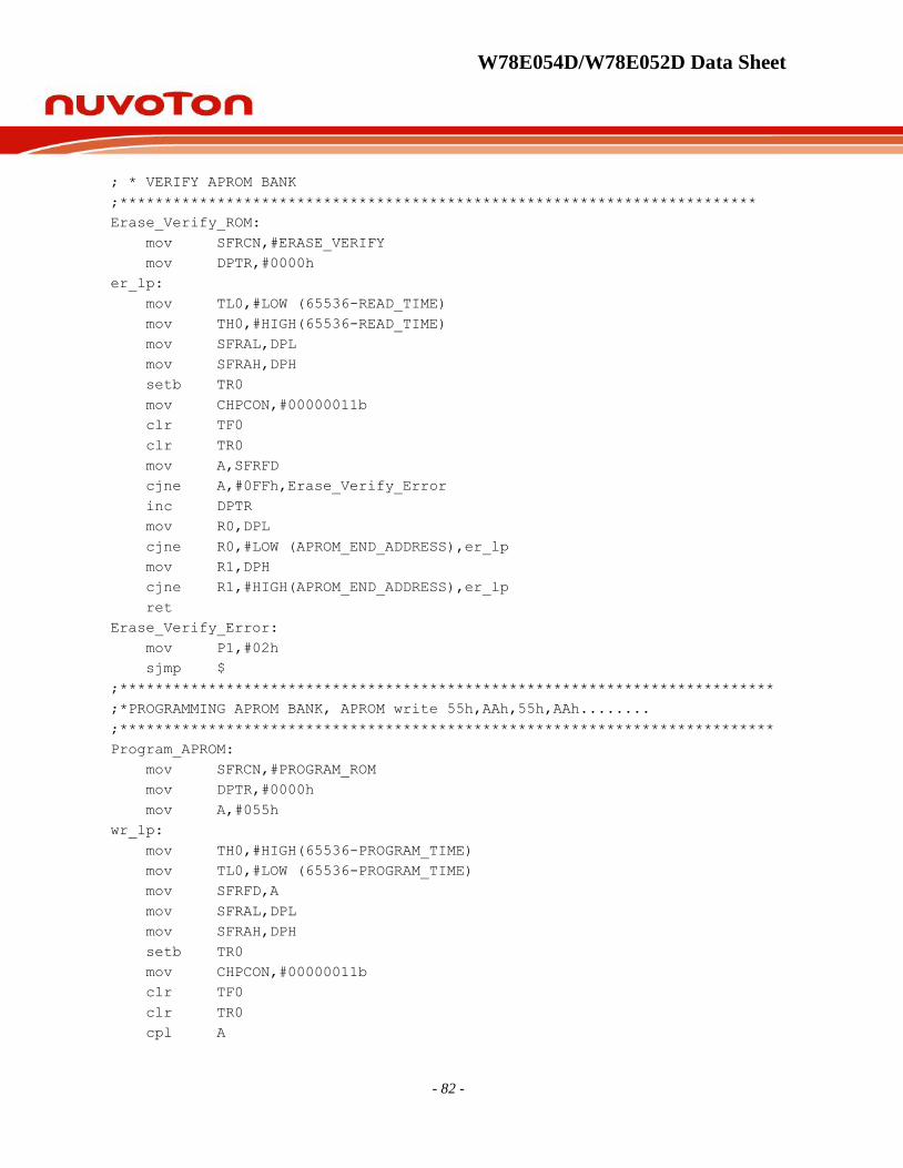
W78E054D/W78E052D Data Sheet
- 82 -
; * VERIFY APROM BANK
;************************************************************************
Erase_Verify_ROM:
mov SFRCN,#ERASE_VERIFY
mov DPTR,#0000h
er_lp:
mov TL0,#LOW (65536-READ_TIME)
mov TH0,#HIGH(65536-READ_TIME)
mov SFRAL,DPL
mov SFRAH,DPH
setb TR0
mov CHPCON,#00000011b
clr TF0
clr TR0
mov A,SFRFD
cjne A,#0FFh,Erase_Verify_Error
inc DPTR
mov R0,DPL
cjne R0,#LOW (APROM_END_ADDRESS),er_lp
mov R1,DPH
cjne R1,#HIGH(APROM_END_ADDRESS),er_lp
ret
Erase_Verify_Error:
mov P1,#02h
sjmp $
;**************************************************************************
;*PROGRAMMING APROM BANK, APROM write 55h,AAh,55h,AAh........
;**************************************************************************
Program_APROM:
mov SFRCN,#PROGRAM_ROM
mov DPTR,#0000h
mov A,#055h
wr_lp:
mov TH0,#HIGH(65536-PROGRAM_TIME)
mov TL0,#LOW (65536-PROGRAM_TIME)
mov SFRFD,A
mov SFRAL,DPL
mov SFRAH,DPH
setb TR0
mov CHPCON,#00000011b
clr TF0
clr TR0
cpl A

W78E054D/W78E052D Data Sheet
Publication Release Date: Aug 31, 2012
- 83 - Revision A12
inc DPTR
mov R0,DPL
cjne R0,#LOW (APROM_END_ADDRESS),wr_lp
mov R1,DPH
cjne R1,#HIGH(APROM_END_ADDRESS),wr_lp
ret
;**************************************************************************
;*Program Verify APROM BANK, read APROM 55h,AAh,55h,AAh........
;**************************************************************************
Program_Verify_APROM:
mov SFRCN,#PROGRAM_VERIFY_ROM
mov DPTR,#0000h
mov B,#055h
rd_lp:
mov TH0,#HIGH(65536-READ_TIME)
mov TL0,#LOW (65536-READ_TIME)
mov SFRAL,DPL
mov SFRAH,DPH
setb TR0
mov CHPCON,#00000011b
clr TF0
clr TR0
mov A,SFRFD
cjne A,B,Program_Fail
mov A,B
cpl A
mov B,A
inc DPTR
mov R0,DPL
cjne R0,#LOW (APROM_END_ADDRESS),rd_lp
mov R1,DPH
cjne R1,#HIGH(APROM_END_ADDRESS),rd_lp
ret
Program_Fail:
mov P1,#03h
sjmp $
;**************************************************************************
;* PROGRAMMING COMPLETLY, SOFTWARE RESET CPU TO APROM
;**************************************************************************
Software_Reset:
MOV CHPCON,#081h ;CHPCON=081h, SOFTWARE RESET to APROM.
sjmp $
end

W78E054D/W78E052D Data Sheet
- 84 -
23 PACKAGE DIMENSIONS
23.1 40-pin DIP
1.371.220.0540.048
SymbolMin Nom Max MaxNomMin
Dimension in inch Dimension in mm
A
B
c
D
e
A
L
S
AA
1
2
E
0.050 1.27
0.210 5.33
0.010
0.150
0.016
0.155
0.018
0.160
0.022
3.81
0.41
0.25
3.94
0.46
4.06
0.56
0.008
0.120
0.670
0.010
0.130
0.014
0.140
0.20
3.05
0.25
3.30
0.36
3.56
0.540 0.5500.545 13.72 13.9713.84
17.02
15.2414.99 15.490.6000.590 0.610
2.29 2.54 2.790.090 0.100 0.110
B1
1
e
E1
2.055 2.070 52.20 52.58
0 15
0.090 2.29
0.6500.630 16.00 16.51
150
Seating Plane
eA
2
A
c
E
Base Plane1
A
1e
L
A
S
1
E
D
1B
B
40 21
201
α
α

W78E054D/W78E052D Data Sheet
Publication Release Date: Aug 31, 2012
- 85 - Revision A12
23.2 44-pin PLCC
44 40
39
29
2818
17
7
6 1
L
c
1b
2
A
H
D
D
e b
E HE
y
A
A1
Seating Plane
DG
GE
SymbolMin Nom Max MaxNomMin
Dimension in inch Dimension in mm
A
bc
D
e
HE
Ly
A
A
1
2
E
b 1
HD
G
GD
E
0.020
0.145
0.026
0.016
0.008
0.648
0.590
0.680
0.090
0.150
0.028
0.018
0.010
0.653
0.610
0.690
0.100
0.050 BSC
0.185
0.155
0.032
0.022
0.014
0.658
0.630
0.700
0.110
0.004
0.51
3.68
0.66
0.41
0.20
16.46
14.99
17.27
2.29
3.81
0.71
0.46
0.25
16.59
15.49
17.53
2.54
1.27
4.70
3.94
0.81
0.56
0.36
16.71
16.00
17.78
2.79
0.10
BSC
16.7116.5916.460.6580.6530.648
16.0015.4914.990.6300.6100.590
17.7817.5317.270.7000.6900.680

W78E054D/W78E052D Data Sheet
- 86 -
23.3 44-pin PQFP
0.250.100.0100.004
SymbolMin Nom Max MaxNomMin
Dimension in inch Dimension in mm
A
bc
D
e
HD
HE
L
y
0
AA
L1
1
2
E
0.006 0.15
- -
0.002
0.075
0.01
0.081
0.014
0.087
0.018
1.90
0.25
0.05
2.05
0.35
2.20
0.45
0.390
0.510
0.025
0.063
0.004
0 10
0.394
0.520
0.031
0.398
0.530
0.037
9.9
0.80
12.95
0.65
1.60
10.00
13.20
0.8
10.1
13.45
0.95
0.3980.3940.390
0.5300.5200.510 13.4513.2012.95
10.110.009.9
100
0.10
.0315
0.01 0.02 0.25 0.5
Seating Plane
11
2212
See Detail F
e b
Ay1
A A2
L
L 1
c
EE
H
1
D
44
H
D
34
33
Detail F

W78E054D/W78E052D Data Sheet
Publication Release Date: Aug 31, 2012
- 87 - Revision A12
23.4 48-pin LQFP

W78E054D/W78E052D Data Sheet
- 88 -
23.5 44-pin TQFP
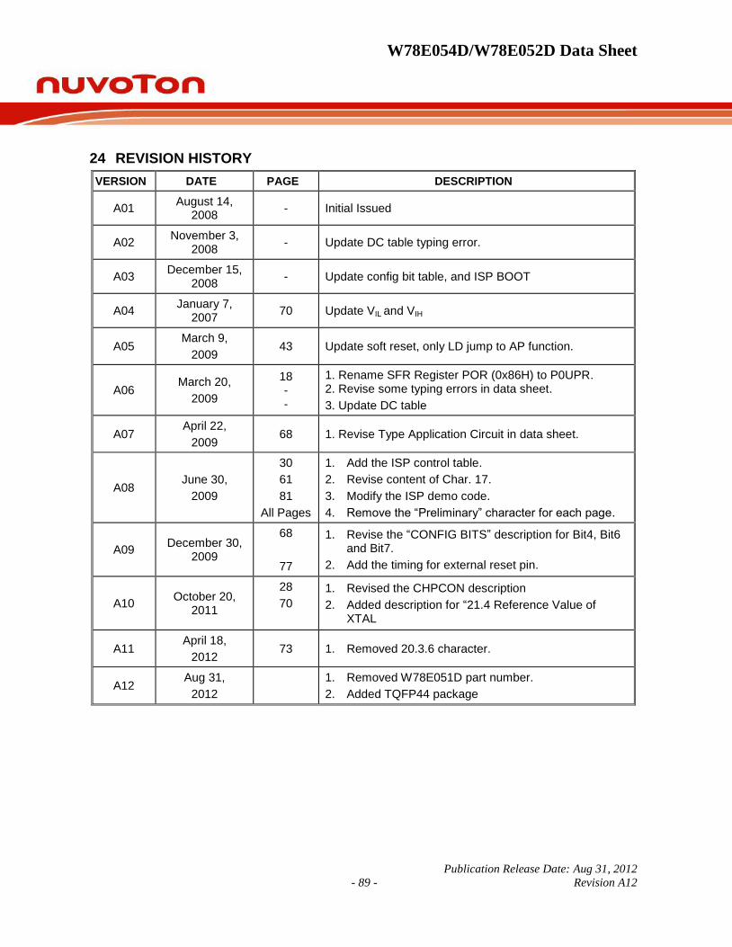
W78E054D/W78E052D Data Sheet
Publication Release Date: Aug 31, 2012
- 89 - Revision A12
24 REVISION HISTORY
VERSION DATE PAGE DESCRIPTION
A01 August 14,
2008 - Initial Issued
A02 November 3,
2008 - Update DC table typing error.
A03 December 15,
2008 - Update config bit table, and ISP BOOT
A04 January 7,
2007 70 Update VIL and VIH
A05 March 9,
2009 43 Update soft reset, only LD jump to AP function.
A06 March 20,
2009
18 - -
1. Rename SFR Register POR (0x86H) to P0UPR. 2. Revise some typing errors in data sheet.
3. Update DC table
A07 April 22,
2009 68 1. Revise Type Application Circuit in data sheet.
A08 June 30,
2009
30
61
81
All Pages
1. Add the ISP control table.
2. Revise content of Char. 17.
3. Modify the ISP demo code.
4. Remove the “Preliminary” character for each page.
A09 December 30,
2009
68
77
1. Revise the “CONFIG BITS” description for Bit4, Bit6 and Bit7.
2. Add the timing for external reset pin.
A10 October 20,
2011
28
70
1. Revised the CHPCON description
2. Added description for “21.4 Reference Value of XTAL
A11 April 18,
2012 73 1. Removed 20.3.6 character.
A12 Aug 31,
2012
1. Removed W78E051D part number.
2. Added TQFP44 package
W78E054D/W78E052D Data Sheet
- 90 -
Important Notice
Nuvoton Products are neither intended nor warranted for usage in systems or equipment, any malfunction or failure of which may cause loss of human life, bodily injury or severe property damage. Such applications are deemed, “Insecure Usage”.
Insecure usage includes, but is not limited to: equipment for surgical implementation, atomic energy control instruments, airplane or spaceship instruments, the control or operation of dy-namic, brake or safety systems designed for vehicular use, traffic signal instruments, all types of safety devices, and other applications intended to support or sustain life.
All Insecure Usage shall be made at customer’s risk, and in the event that third parties lay claims to Nuvoton as a result of customer’s Insecure Usage, customer shall indemnify the dam-ages and liabilities thus incurred by Nuvoton.