w iti - mouser.com
TRANSCRIPT

Following the acquisi�on of Adesto Technologies, Dialog Semiconductor offers memory products as part of its product por�olio. The exis�ng content from datasheets, including part numbers and codes should be used. Terms of Purchase are provided on the Dialog website
https://www.dialog-semiconductor.com/general-terms-and-conditions-purchase
View our Dialog memory products por�olio:
www.dialog-semiconductor.com/products/memory
Contacting Dialog SemiconductorUnited Kingdom (Headquarters)Dialog Semiconductor (UK) LTDPhone: +44 1793 757700GermanyDialog Semiconductor GmbHPhone: +49 7021 805-0The NetherlandsDialog Semiconductor B.V.Phone: +31 73 640 8822Email:[email protected]
North AmericaDialog Semiconductor Inc.Phone: +1 408 845 8500JapanDialog Semiconductor K. K.Phone: +81 3 5769 5100TaiwanDialog Semiconductor TaiwanPhone: +886 281 786 222Web site:www.dialog-semiconductor.com
China (Shenzhen)Dialog Semiconductor ChinaPhone: +86 755 2981 3669China (Shanghai)Dialog Semiconductor ChinaPhone: +86 21 5424 9058#
Hong KongDialog Semiconductor Hong KongPhone: +852 2607 4271KoreaDialog Semiconductor KoreaPhone: +82 2 3469 8200

DS-AT25FF081A–183D–2021-01
PRELIMINARY DATASHEET
AT25FF081A8 Mbit, 1.65V - 3.6V RangeSPI Serial Flash Memory with Multi-I/O Support
Features Voltage Range: 1.65V - 3.6V 8 Mbit (2M x 4) Flash Memory Serial Peripheral Interface (SPI) compatible
- Supports SPI modes 0 and 3 (1-1-1)- Supports dual output operation (1-1-2)- Supports quad output operation (1-1-4)- Supports quad I/O operation (1-4-4)- Supports XiP operation (1-4-4, 0-4-4)
133 MHz maximum operating frequency- Clock-to-output of 8 ns
Flexible, optimized erase architecture for code + data storage applications- Uniform 4-KByte block erase- Uniform 32-KByte block erase- Uniform 64-KByte block erase- Full chip erase
Flexible non-volatile block protection 1 x 128-byte factory-programmed unique identifier 3 x 128-byte, One Time Programmable (OTP) security registers Flexible programming
- Byte/Page program (1 to 256 Bytes)- Sequential program mode capability
Erase program suspend resume Software controlled Reset and Terminate commands Hardware reset option (via HOLD pin) JEDEC hardware reset Non-volatile status register configuration option JEDEC standard manufacturer and device ID read methodology Serial Flash Discoverable Parameters (SFDP) version 1.6 Low power dissipation:
- 30 µA standby current (typical)- 8.5 µA Deep Power-Down (DPD) current (typical)- 7 nA Ultra Deep Power Down (UDPD) current (typical)- 8.5 mA active read current (1-1-1 — 104 MHz)- 9.1 mA program current- 10.4 mA erase current
User configurable and auto I/O pin drive levels Endurance
- 100,000 program/erase cycles Data Retention
- 20 years Temperature Range
- -40 oC to +85 oC Industry standard green (Pb/Halide-free/RoHS Compliant) Package Options
- 8-lead SOIC (150-mil)- 8-lead SOIC (208-mil)- 8-pad Ultra-thin DFN (2 x 3 x 0.6 mm)- 8-ball WLCSP (3 x 2 x 3 ball matrix)- Die in Wafer Form (DWF)
2AT25FF081A DS-AT25FF081A–183D–2021-01
1. Product OverviewThe Adesto® AT25FF081A is a serial interface Flash memory device designed for use in a wide variety of high-volume consumer and connected applications. It is optimized for low-energy applications and can be operated using modern Lithium battery technologies over a wide input voltage range of 1.65V - 3.6V.
The AT25FF081A is ideally suited for systems in which program code is shadowed from Flash memory into embedded or external RAM (code shadow) for execution, and where small amounts of data are stored and updated locally in the Flash memory.
The erase block sizes of the AT25FF081A have been optimized to meet the needs of today's code and data storage applications. The device supports 4 KiloByte (KB), 32 KB, and 64 KB block erase operations and a full-chip erase. By optimizing the size of the erase blocks, the memory space can be used much more efficiently.
The device contains four specialized 128-byte One-Time Programmable (OTP) security registers that can be used to store a unique device ID and locked key storage.
Specifically designed for use in a wide variety of systems, the AT25FF081A supports read, program, and erase operations. No separate voltage is required for programming and erasing.
Throughout this document, the term Multi-I/O is used generically to refer to all of the multiple I/O modes, including dual, quad, and XiP.
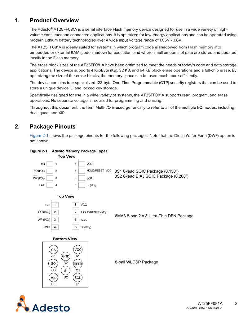
2. Package PinoutsFigure 2-1 shows the package pinouts for the following packages. Note that the Die in Wafer Form (DWF) option is not shown.
Figure 2-1. Adesto Memory Package Types
CS
GND
VCC
SCK
1
2
3
4
8
7
6
5
SO (I/O1) HOLD/RESET (I/O3)
SI (I/O0)
WP (I/O2)
1
2
3
4
8
7
6
5
CS
SO (I/O1)
WP (I/O2)
GND
VCC
HOLD/RESET (I/O3)
SCK
SI (I/O0)
8S1 8-lead SOIC Package (0.150”)8S2 8-lead EIAJ SOIC Package (0.208”)
8MA3 8-pad 2 x 3 Ultra-Thin DFN Package
8-ball WLCSP Package
Top View
Top View
Bottom View
3AT25FF081A DS-AT25FF081A–183D–2021-01
Table of Contents1. Product Overview . . . . . . . . . . . . . . . . . . . . . . . . . . . . . . . . . . . . . . . . . . . . . . . . . . . . . . . . . . . . . . . . . . . . 22. Package Pinouts . . . . . . . . . . . . . . . . . . . . . . . . . . . . . . . . . . . . . . . . . . . . . . . . . . . . . . . . . . . . . . . . . . . . . 23. Block Diagram . . . . . . . . . . . . . . . . . . . . . . . . . . . . . . . . . . . . . . . . . . . . . . . . . . . . . . . . . . . . . . . . . . . . . . 54. Pin Descriptions . . . . . . . . . . . . . . . . . . . . . . . . . . . . . . . . . . . . . . . . . . . . . . . . . . . . . . . . . . . . . . . . . . . . . 65. Device Operation . . . . . . . . . . . . . . . . . . . . . . . . . . . . . . . . . . . . . . . . . . . . . . . . . . . . . . . . . . . . . . . . . . . . 8
5.1 Data Transfer Modes . . . . . . . . . . . . . . . . . . . . . . . . . . . . . . . . . . . . . . . . . . . . . . . . . . . . . . . . . . . . 85.2 Standard SPI Operation . . . . . . . . . . . . . . . . . . . . . . . . . . . . . . . . . . . . . . . . . . . . . . . . . . . . . . . . . . 85.3 Dual Output Operation (1-1-2) . . . . . . . . . . . . . . . . . . . . . . . . . . . . . . . . . . . . . . . . . . . . . . . . . . . . 115.4 Quad Output Operation (1-1-4). . . . . . . . . . . . . . . . . . . . . . . . . . . . . . . . . . . . . . . . . . . . . . . . . . . . 125.5 Quad I/O Operation (1-4-4). . . . . . . . . . . . . . . . . . . . . . . . . . . . . . . . . . . . . . . . . . . . . . . . . . . . . . . 135.6 XiP Mode Operation . . . . . . . . . . . . . . . . . . . . . . . . . . . . . . . . . . . . . . . . . . . . . . . . . . . . . . . . . . . . 145.7 Memory Architecture. . . . . . . . . . . . . . . . . . . . . . . . . . . . . . . . . . . . . . . . . . . . . . . . . . . . . . . . . . . . 175.8 Memory Protection . . . . . . . . . . . . . . . . . . . . . . . . . . . . . . . . . . . . . . . . . . . . . . . . . . . . . . . . . . . . . 205.9 Power Down Considerations. . . . . . . . . . . . . . . . . . . . . . . . . . . . . . . . . . . . . . . . . . . . . . . . . . . . . . 235.10 Erase/Program Suspend Considerations and Nested Operations . . . . . . . . . . . . . . . . . . . . . . . . . 255.11 OTP Security Register Lock . . . . . . . . . . . . . . . . . . . . . . . . . . . . . . . . . . . . . . . . . . . . . . . . . . . . . . 315.12 Standard JEDEC Hardware Reset . . . . . . . . . . . . . . . . . . . . . . . . . . . . . . . . . . . . . . . . . . . . . . . . . 315.13 Chip Select Restrictions . . . . . . . . . . . . . . . . . . . . . . . . . . . . . . . . . . . . . . . . . . . . . . . . . . . . . . . . . 325.14 HOLD / RESET Function . . . . . . . . . . . . . . . . . . . . . . . . . . . . . . . . . . . . . . . . . . . . . . . . . . . . . . . . 33
6. Status Registers . . . . . . . . . . . . . . . . . . . . . . . . . . . . . . . . . . . . . . . . . . . . . . . . . . . . . . . . . . . . . . . . . . . . 346.1 Register Structure and Updates . . . . . . . . . . . . . . . . . . . . . . . . . . . . . . . . . . . . . . . . . . . . . . . . . . . 346.2 Register Accesses . . . . . . . . . . . . . . . . . . . . . . . . . . . . . . . . . . . . . . . . . . . . . . . . . . . . . . . . . . . . . 356.3 Status Register 1 . . . . . . . . . . . . . . . . . . . . . . . . . . . . . . . . . . . . . . . . . . . . . . . . . . . . . . . . . . . . . . 366.4 Status Register 2 . . . . . . . . . . . . . . . . . . . . . . . . . . . . . . . . . . . . . . . . . . . . . . . . . . . . . . . . . . . . . . 386.5 Status Register 3 . . . . . . . . . . . . . . . . . . . . . . . . . . . . . . . . . . . . . . . . . . . . . . . . . . . . . . . . . . . . . . 406.6 Status Register 4 . . . . . . . . . . . . . . . . . . . . . . . . . . . . . . . . . . . . . . . . . . . . . . . . . . . . . . . . . . . . . . 416.7 Status Register 5 . . . . . . . . . . . . . . . . . . . . . . . . . . . . . . . . . . . . . . . . . . . . . . . . . . . . . . . . . . . . . . 43
7. Commands and Addressing . . . . . . . . . . . . . . . . . . . . . . . . . . . . . . . . . . . . . . . . . . . . . . . . . . . . . . . . . . . 447.1 Read Array (03h, 0Bh) . . . . . . . . . . . . . . . . . . . . . . . . . . . . . . . . . . . . . . . . . . . . . . . . . . . . . . . . . . 487.2 Dual Output Read Array (3Bh) . . . . . . . . . . . . . . . . . . . . . . . . . . . . . . . . . . . . . . . . . . . . . . . . . . . . 497.3 Quad Output Read Array (6Bh) . . . . . . . . . . . . . . . . . . . . . . . . . . . . . . . . . . . . . . . . . . . . . . . . . . . 507.4 XiP Read (EBh), XiP Read with Double-word Aligned Address (E7h) . . . . . . . . . . . . . . . . . . . . . . 517.5 Block Erase (20h, 52h, D8h). . . . . . . . . . . . . . . . . . . . . . . . . . . . . . . . . . . . . . . . . . . . . . . . . . . . . . 557.6 Chip Erase (60h, C7h) . . . . . . . . . . . . . . . . . . . . . . . . . . . . . . . . . . . . . . . . . . . . . . . . . . . . . . . . . . 577.7 Byte/Page Program (02h) . . . . . . . . . . . . . . . . . . . . . . . . . . . . . . . . . . . . . . . . . . . . . . . . . . . . . . . . 587.8 Sequential Program Mode (ADh/AFh) . . . . . . . . . . . . . . . . . . . . . . . . . . . . . . . . . . . . . . . . . . . . . . 607.9 Dual Output Byte/Page Program (A2h). . . . . . . . . . . . . . . . . . . . . . . . . . . . . . . . . . . . . . . . . . . . . . 647.10 Quad Output Page Program (32h) . . . . . . . . . . . . . . . . . . . . . . . . . . . . . . . . . . . . . . . . . . . . . . . . . 667.11 Program/Erase Suspend (75h/B0h) . . . . . . . . . . . . . . . . . . . . . . . . . . . . . . . . . . . . . . . . . . . . . . . . 687.12 Program/Erase Resume (7Ah/D0h) . . . . . . . . . . . . . . . . . . . . . . . . . . . . . . . . . . . . . . . . . . . . . . . . 717.13 Set Burst Wrap (77h) . . . . . . . . . . . . . . . . . . . . . . . . . . . . . . . . . . . . . . . . . . . . . . . . . . . . . . . . . . . 73
4AT25FF081A DS-AT25FF081A–183D–2021-01
Table of Contents7.14 Write Enable (06h) . . . . . . . . . . . . . . . . . . . . . . . . . . . . . . . . . . . . . . . . . . . . . . . . . . . . . . . . . . . . . 757.15 Write Disable (04h) . . . . . . . . . . . . . . . . . . . . . . . . . . . . . . . . . . . . . . . . . . . . . . . . . . . . . . . . . . . . . 767.16 Volatile Status Register Write Enable (50h) . . . . . . . . . . . . . . . . . . . . . . . . . . . . . . . . . . . . . . . . . . 777.17 Individual Block Lock (36h) . . . . . . . . . . . . . . . . . . . . . . . . . . . . . . . . . . . . . . . . . . . . . . . . . . . . . . . 787.18 Individual Block Unlock (39h) . . . . . . . . . . . . . . . . . . . . . . . . . . . . . . . . . . . . . . . . . . . . . . . . . . . . . 797.19 Read Block Lock (3Ch/3Dh) . . . . . . . . . . . . . . . . . . . . . . . . . . . . . . . . . . . . . . . . . . . . . . . . . . . . . . 807.20 Global Block Lock (7Eh) . . . . . . . . . . . . . . . . . . . . . . . . . . . . . . . . . . . . . . . . . . . . . . . . . . . . . . . . . 817.21 Global Block Unlock (98h) . . . . . . . . . . . . . . . . . . . . . . . . . . . . . . . . . . . . . . . . . . . . . . . . . . . . . . . 827.22 Program Security Register (9Bh) . . . . . . . . . . . . . . . . . . . . . . . . . . . . . . . . . . . . . . . . . . . . . . . . . . 837.23 Read OTP Security Register (4Bh). . . . . . . . . . . . . . . . . . . . . . . . . . . . . . . . . . . . . . . . . . . . . . . . . 867.24 Read Status Registers 1 - 3 (05h, 35h, 15h) . . . . . . . . . . . . . . . . . . . . . . . . . . . . . . . . . . . . . . . . . 877.25 Read Status Registers (65h). . . . . . . . . . . . . . . . . . . . . . . . . . . . . . . . . . . . . . . . . . . . . . . . . . . . . . 887.26 Write Status Registers 1 - 3 — Direct (01h, 31h, 11h) . . . . . . . . . . . . . . . . . . . . . . . . . . . . . . . . . . 907.27 Write Status Registers — Indirect (71h) . . . . . . . . . . . . . . . . . . . . . . . . . . . . . . . . . . . . . . . . . . . . . 917.28 Status Register Lock (6Fh) . . . . . . . . . . . . . . . . . . . . . . . . . . . . . . . . . . . . . . . . . . . . . . . . . . . . . . . 937.29 Deep Power Down (B9h) . . . . . . . . . . . . . . . . . . . . . . . . . . . . . . . . . . . . . . . . . . . . . . . . . . . . . . . . 947.30 Resume from Ultra-Deep Power Down / Deep Power Down with Device ID (ABh) . . . . . . . . . . . . 957.31 Ultra-Deep Power Down (79h) . . . . . . . . . . . . . . . . . . . . . . . . . . . . . . . . . . . . . . . . . . . . . . . . . . . . 977.32 Enable Reset (66h) and Reset Device (99h) . . . . . . . . . . . . . . . . . . . . . . . . . . . . . . . . . . . . . . . . . 997.33 Terminate (F0h) . . . . . . . . . . . . . . . . . . . . . . . . . . . . . . . . . . . . . . . . . . . . . . . . . . . . . . . . . . . . . . 1007.34 Read Manufacturer/Device ID (90h) . . . . . . . . . . . . . . . . . . . . . . . . . . . . . . . . . . . . . . . . . . . . . . . 1017.35 Quad I/O Read Manufacturer/Device ID (94h) . . . . . . . . . . . . . . . . . . . . . . . . . . . . . . . . . . . . . . . 1027.36 Read JEDEC ID (9Fh) . . . . . . . . . . . . . . . . . . . . . . . . . . . . . . . . . . . . . . . . . . . . . . . . . . . . . . . . . 1037.37 Serial Flash Discoverable Parameters (5Ah) . . . . . . . . . . . . . . . . . . . . . . . . . . . . . . . . . . . . . . . . 106
8. Electrical Specifications . . . . . . . . . . . . . . . . . . . . . . . . . . . . . . . . . . . . . . . . . . . . . . . . . . . . . . . . . . . . . 1078.1 Absolute Maximum Ratings . . . . . . . . . . . . . . . . . . . . . . . . . . . . . . . . . . . . . . . . . . . . . . . . . . . . . 1078.2 DC and AC Operating Range . . . . . . . . . . . . . . . . . . . . . . . . . . . . . . . . . . . . . . . . . . . . . . . . . . . . 1078.3 DC Characteristics . . . . . . . . . . . . . . . . . . . . . . . . . . . . . . . . . . . . . . . . . . . . . . . . . . . . . . . . . . . . 1078.4 AC Characteristics - Maximum Clock Frequencies. . . . . . . . . . . . . . . . . . . . . . . . . . . . . . . . . . . . 1088.5 AC Characteristics – All Other Parameters. . . . . . . . . . . . . . . . . . . . . . . . . . . . . . . . . . . . . . . . . . 1088.6 Program and Erase Characteristics . . . . . . . . . . . . . . . . . . . . . . . . . . . . . . . . . . . . . . . . . . . . . . . 1108.7 Power On Timing . . . . . . . . . . . . . . . . . . . . . . . . . . . . . . . . . . . . . . . . . . . . . . . . . . . . . . . . . . . . . 1118.8 AC Timing Diagrams. . . . . . . . . . . . . . . . . . . . . . . . . . . . . . . . . . . . . . . . . . . . . . . . . . . . . . . . . . . 112
9. Ordering Information . . . . . . . . . . . . . . . . . . . . . . . . . . . . . . . . . . . . . . . . . . . . . . . . . . . . . . . . . . . . . . . . 11410. Packaging Information . . . . . . . . . . . . . . . . . . . . . . . . . . . . . . . . . . . . . . . . . . . . . . . . . . . . . . . . . . . . . . 115
10.1 8S1 – JEDEC SOIC . . . . . . . . . . . . . . . . . . . . . . . . . . . . . . . . . . . . . . . . . . . . . . . . . . . . . . . . . . . 11610.2 8S2 – 8-lead EIAJ SOIC . . . . . . . . . . . . . . . . . . . . . . . . . . . . . . . . . . . . . . . . . . . . . . . . . . . . . . . . 11710.3 8MA3 – 2 x 3 UDFN . . . . . . . . . . . . . . . . . . . . . . . . . . . . . . . . . . . . . . . . . . . . . . . . . . . . . . . . . . . 11810.4 8-WLCSP — 8-ball 3 x 2 x 3 WLCSP . . . . . . . . . . . . . . . . . . . . . . . . . . . . . . . . . . . . . . . . . . . . . . 119
11. Revision History . . . . . . . . . . . . . . . . . . . . . . . . . . . . . . . . . . . . . . . . . . . . . . . . . . . . . . . . . . . . . . . . . . . 120
5AT25FF081A DS-AT25FF081A–183D–2021-01
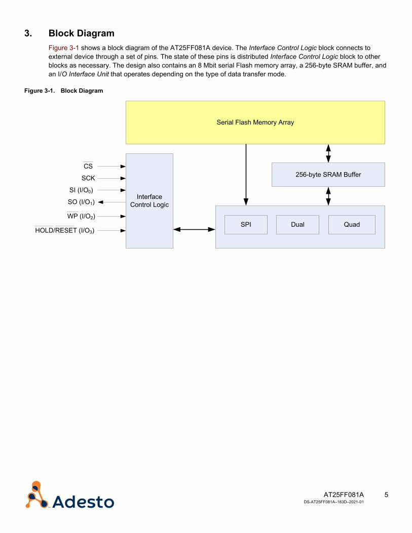
3. Block DiagramFigure 3-1 shows a block diagram of the AT25FF081A device. The Interface Control Logic block connects to external device through a set of pins. The state of these pins is distributed Interface Control Logic block to other blocks as necessary. The design also contains an 8 Mbit serial Flash memory array, a 256-byte SRAM buffer, and an I/O Interface Unit that operates depending on the type of data transfer mode.
Figure 3-1. Block Diagram
CS
SCK
SI (I/O0)
SO (I/O1)
WP (I/O2)
HOLD/RESET (I/O3)
Interface Control Logic
256-byte SRAM Buffer
SPI Dual Quad
Serial Flash Memory Array

6AT25FF081A DS-AT25FF081A–183D–2021-01
4. Pin DescriptionsTable 4-1. Pin Descriptions
Symbol Name and FunctionAsserted
State Type
CS
CHIP SELECT: Asserting the CS pin selects the device. When the CS pin is deasserted, the device is be deselected and normally be placed in standby mode (not Deep Power-Down mode), and the SO pin is in a high-impedance state. When the device is deselected, data will not be accepted on the SI pin.A high-to-low transition on the CS pin is required to start an operation, and a low-to-high transition is required to end an operation. When ending an internally self-timed operation such as a program or erase cycle, the device will not enter the standby mode until the completion of the operation.
Low Input
SCK
SERIAL CLOCK: This pin is used to provide a clock to the device and is used to control the flow of data to and from the device. Command, address, and input data present on the SI pin is always latched in on the rising edge of SCK, while output data on the SO pin is always clocked out on the falling edge of SCK.
- Input
SI (I/O0)
SERIAL INPUT: The SI pin is used to shift data into the device. The SI pin is used for all data input including command and address sequences. Data on the SI pin is always latched in on the rising edge of SCK.With the Multi I/O Read commands, the SI pin becomes an output pin (I/O0) in conjunction with other pins to allow either two or four bits of data on (I/O1:0 or I/O3:0) to be clocked out on every falling edge of SCK.Data present on the SI pin is ignored whenever the device is deselected (CS is deasserted and the device is in the reset condition).
- Input/Output
SO (I/O1)
SERIAL OUTPUT: The SO pin is used to shift data out from the device. Data on the SO pin is always clocked out on the falling edge of SCK.With the Multi I/O Read commands, the SO pin remains an output pin (I/O1) in conjunction with other pins to allow either two or four bits of data on (I/O1:0 or I/O3:0) to be clocked out on every falling edge of SCK.The SO pin is in a high-impedance state whenever the device is deselected (CS is deasserted and the device is in the reset condition).
- Input/Output
WP (I/O2)
WRITE PROTECT: The WP pin controls the hardware locking feature of the device. When set, this bit prevents the Status Register from being written. This bit is used in conjunction with other Status Register bits (CMPRT, BPSIZE, TB, and BP[2:0]) to provide hardware protection of the memory array. The WP pin is internally pulled-high and may be left floating if hardware controlled protection will not be used. However, it is recommended that the WP pin also be externally connected to VCC whenever possible.When the QE bit in Status Register 2 is set, enabling quad mode (Output or I/O), the WP pin becomes bidirectional and functions as the IO2 pin used to transmit address and/or data, depending on the transfer mode.
Low Input/Output
7AT25FF081A DS-AT25FF081A–183D–2021-01
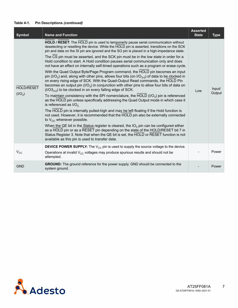
HOLD/RESET(I/O3)
HOLD / RESET: The HOLD pin is used to temporarily pause serial communication without deselecting or resetting the device. While the HOLD pin is asserted, transitions on the SCK pin and data on the SI pin are ignored and the SO pin is placed in a high-impedance state.The CS pin must be asserted, and the SCK pin must be in the low state in order for a Hold condition to start. A Hold condition pauses serial communication only and does not have an effect on internally self-timed operations such as a program or erase cycle.With the Quad Output Byte/Page Program command, the HOLD pin becomes an input pin (I/O3) and, along with other pins, allows four bits (on I/O3-0) of data to be clocked in on every rising edge of SCK. With the Quad-Output Read commands, the HOLD Pin becomes an output pin (I/O3) in conjunction with other pins to allow four bits of data on (I/O33-0) to be clocked in on every falling edge of SCK.To maintain consistency with the SPI nomenclature, the HOLD (I/O3) pin is referenced as the HOLD pin unless specifically addressing the Quad Output mode in which case it is referenced as I/O3.
The HOLD pin is internally pulled-high and may be left floating if the Hold function is not used. However, it is recommended that the HOLD pin also be externally connected to VCC whenever possible.When the QE bit in the Status register is cleared, the IO3 pin can be configured either as a HOLD pin or as a RESET pin depending on the state of the HOLD/RESET bit 7 in Status Register 3. Note that when the QE bit is set, the HOLD or RESET function is not available as this pin is used to transfer data.
Low Input/Output
VCC
DEVICE POWER SUPPLY: The VCC pin is used to supply the source voltage to the device.Operations at invalid VCC voltages may produce spurious results and should not be attempted.
- Power
GND GROUND: The ground reference for the power supply. GND should be connected to the system ground. - Power
Table 4-1. Pin Descriptions (continued)
Symbol Name and FunctionAsserted
State Type
8AT25FF081A DS-AT25FF081A–183D–2021-01
5. Device OperationThis section describes the various data transfer modes supported by the device, as well as other system operations.
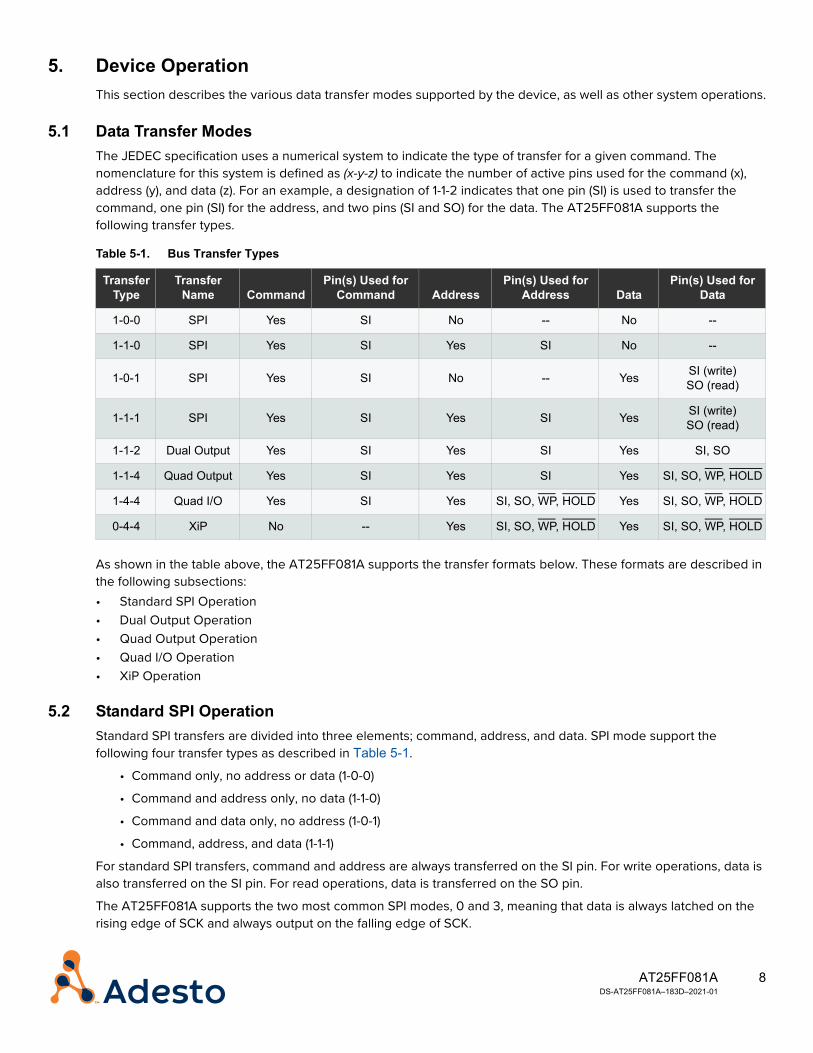
5.1 Data Transfer ModesThe JEDEC specification uses a numerical system to indicate the type of transfer for a given command. The nomenclature for this system is defined as (x-y-z) to indicate the number of active pins used for the command (x), address (y), and data (z). For an example, a designation of 1-1-2 indicates that one pin (SI) is used to transfer the command, one pin (SI) for the address, and two pins (SI and SO) for the data. The AT25FF081A supports the following transfer types.
As shown in the table above, the AT25FF081A supports the transfer formats below. These formats are described in the following subsections:• Standard SPI Operation• Dual Output Operation• Quad Output Operation• Quad I/O Operation• XiP Operation
5.2 Standard SPI OperationStandard SPI transfers are divided into three elements; command, address, and data. SPI mode support the following four transfer types as described in Table 5-1.
• Command only, no address or data (1-0-0)
• Command and address only, no data (1-1-0)
• Command and data only, no address (1-0-1)
• Command, address, and data (1-1-1)
For standard SPI transfers, command and address are always transferred on the SI pin. For write operations, data is also transferred on the SI pin. For read operations, data is transferred on the SO pin.
The AT25FF081A supports the two most common SPI modes, 0 and 3, meaning that data is always latched on the rising edge of SCK and always output on the falling edge of SCK.
Table 5-1. Bus Transfer Types
Transfer Type
Transfer Name Command
Pin(s) Used for Command Address
Pin(s) Used for Address Data
Pin(s) Used for Data
1-0-0 SPI Yes SI No -- No --
1-1-0 SPI Yes SI Yes SI No --
1-0-1 SPI Yes SI No -- Yes SI (write)SO (read)
1-1-1 SPI Yes SI Yes SI Yes SI (write)SO (read)
1-1-2 Dual Output Yes SI Yes SI Yes SI, SO
1-1-4 Quad Output Yes SI Yes SI Yes SI, SO, WP, HOLD
1-4-4 Quad I/O Yes SI Yes SI, SO, WP, HOLD Yes SI, SO, WP, HOLD
0-4-4 XiP No -- Yes SI, SO, WP, HOLD Yes SI, SO, WP, HOLD
9AT25FF081A DS-AT25FF081A–183D–2021-01
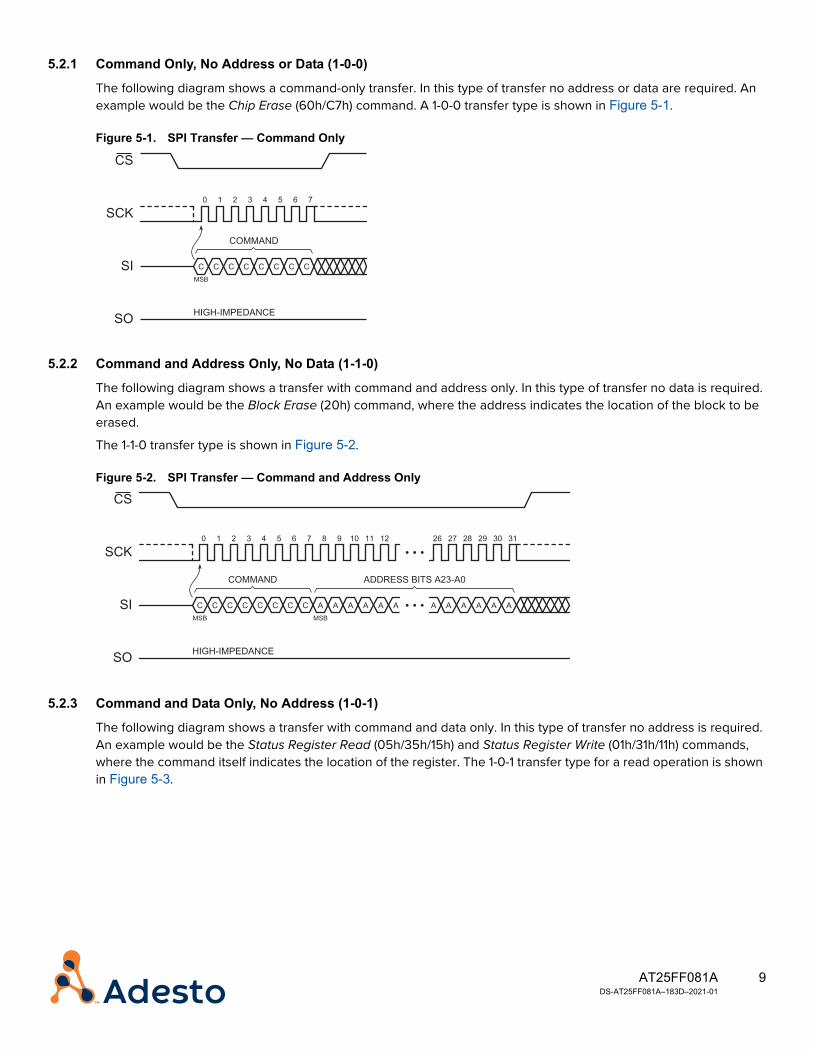
5.2.1 Command Only, No Address or Data (1-0-0)
The following diagram shows a command-only transfer. In this type of transfer no address or data are required. An example would be the Chip Erase (60h/C7h) command. A 1-0-0 transfer type is shown in Figure 5-1.
Figure 5-1. SPI Transfer — Command Only
5.2.2 Command and Address Only, No Data (1-1-0)
The following diagram shows a transfer with command and address only. In this type of transfer no data is required. An example would be the Block Erase (20h) command, where the address indicates the location of the block to be erased.
The 1-1-0 transfer type is shown in Figure 5-2.
Figure 5-2. SPI Transfer — Command and Address Only
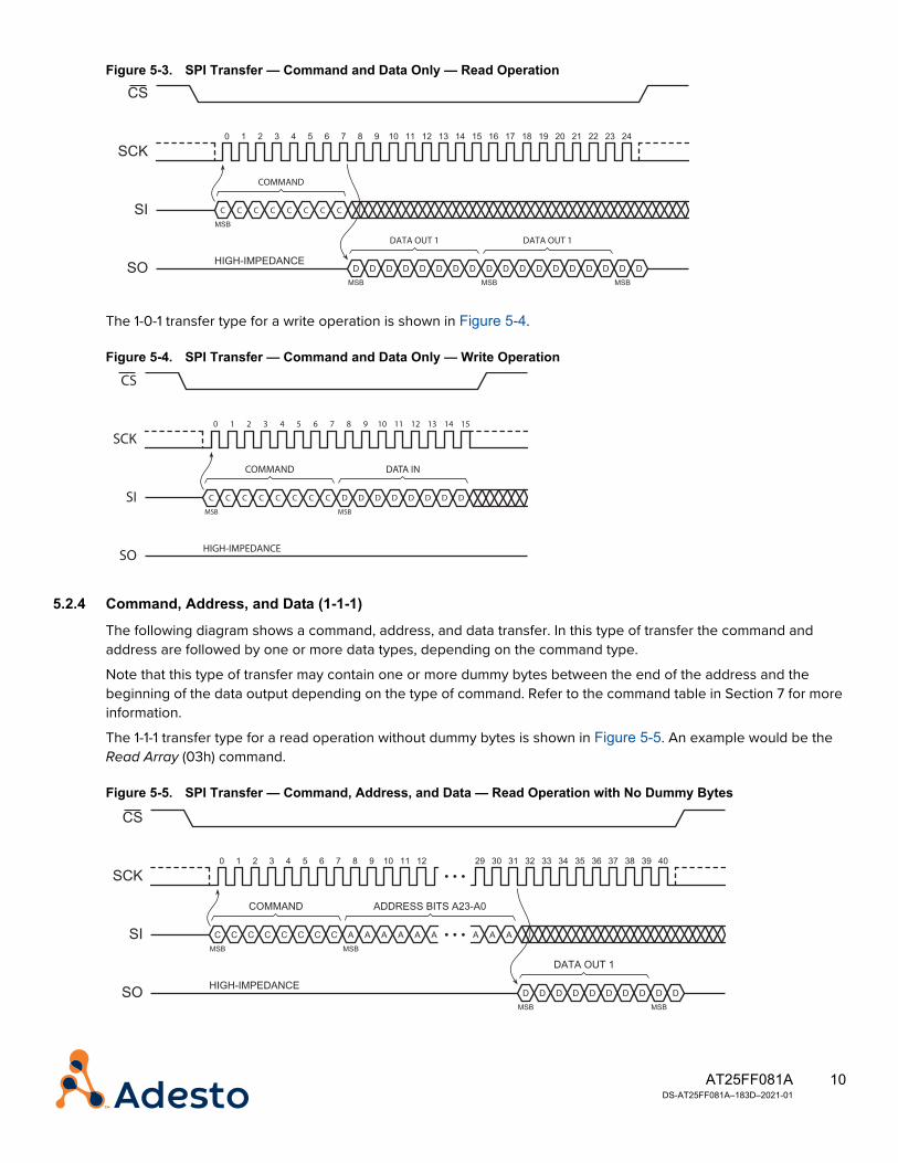
5.2.3 Command and Data Only, No Address (1-0-1)
The following diagram shows a transfer with command and data only. In this type of transfer no address is required. An example would be the Status Register Read (05h/35h/15h) and Status Register Write (01h/31h/11h) commands, where the command itself indicates the location of the register. The 1-0-1 transfer type for a read operation is shown in Figure 5-3.
10AT25FF081A DS-AT25FF081A–183D–2021-01
Figure 5-3. SPI Transfer — Command and Data Only — Read Operation
The 1-0-1 transfer type for a write operation is shown in Figure 5-4.
Figure 5-4. SPI Transfer — Command and Data Only — Write Operation
5.2.4 Command, Address, and Data (1-1-1)
The following diagram shows a command, address, and data transfer. In this type of transfer the command and address are followed by one or more data types, depending on the command type.
Note that this type of transfer may contain one or more dummy bytes between the end of the address and the beginning of the data output depending on the type of command. Refer to the command table in Section 7 for more information.
The 1-1-1 transfer type for a read operation without dummy bytes is shown in Figure 5-5. An example would be the Read Array (03h) command.
Figure 5-5. SPI Transfer — Command, Address, and Data — Read Operation with No Dummy Bytes
SCK
CS
SI
SO
MSB
2 310
C C C C C C C C
6 754 10 1198 12 21 2217 20191815 1613 14 23 24
COMMAND
MSB MSB
D D D D D D D DDDMSB
D D D D D DDD
DATA OUT 1 DATA OUT 1
HIGH-IMPEDANCE
SCK
CS
SI
SO
MSB
2 310
C C C C C C C
6 754 10 1198 14 151312
COMMAND
MSB
C D D D D D D D D
DATA IN
HIGH-IMPEDANCE
11AT25FF081A DS-AT25FF081A–183D–2021-01
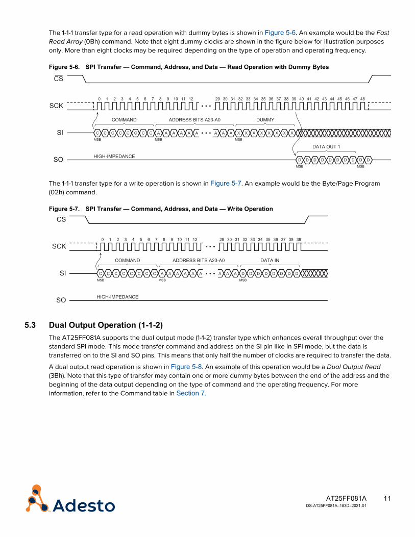
The 1-1-1 transfer type for a read operation with dummy bytes is shown in Figure 5-6. An example would be the Fast Read Array (0Bh) command. Note that eight dummy clocks are shown in the figure below for illustration purposes only. More than eight clocks may be required depending on the type of operation and operating frequency.
Figure 5-6. SPI Transfer — Command, Address, and Data — Read Operation with Dummy Bytes
The 1-1-1 transfer type for a write operation is shown in Figure 5-7. An example would be the Byte/Page Program (02h) command.
Figure 5-7. SPI Transfer — Command, Address, and Data — Write Operation
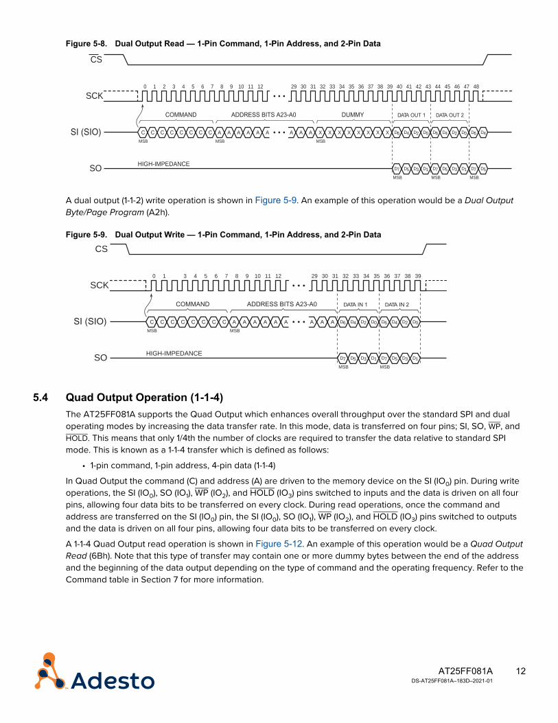
5.3 Dual Output Operation (1-1-2)The AT25FF081A supports the dual output mode (1-1-2) transfer type which enhances overall throughput over the standard SPI mode. This mode transfer command and address on the SI pin like in SPI mode, but the data is transferred on to the SI and SO pins. This means that only half the number of clocks are required to transfer the data.
A dual output read operation is shown in Figure 5-8. An example of this operation would be a Dual Output Read (3Bh). Note that this type of transfer may contain one or more dummy bytes between the end of the address and the beginning of the data output depending on the type of command and the operating frequency. For more information, refer to the Command table in Section 7.
12AT25FF081A DS-AT25FF081A–183D–2021-01
Figure 5-8. Dual Output Read — 1-Pin Command, 1-Pin Address, and 2-Pin Data
A dual output (1-1-2) write operation is shown in Figure 5-9. An example of this operation would be a Dual Output Byte/Page Program (A2h).
Figure 5-9. Dual Output Write — 1-Pin Command, 1-Pin Address, and 2-Pin Data
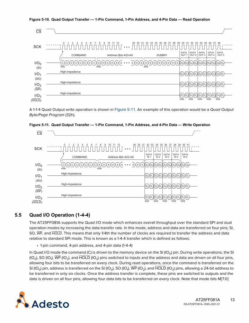
5.4 Quad Output Operation (1-1-4)The AT25FF081A supports the Quad Output which enhances overall throughput over the standard SPI and dual operating modes by increasing the data transfer rate. In this mode, data is transferred on four pins; SI, SO, WP, and HOLD. This means that only 1/4th the number of clocks are required to transfer the data relative to standard SPI mode. This is known as a 1-1-4 transfer which is defined as follows:
• 1-pin command, 1-pin address, 4-pin data (1-1-4)
In Quad Output the command (C) and address (A) are driven to the memory device on the SI (IO0) pin. During write operations, the SI (IO0), SO (IO1), WP (IO2), and HOLD (IO3) pins switched to inputs and the data is driven on all four pins, allowing four data bits to be transferred on every clock. During read operations, once the command and address are transferred on the SI (IO0) pin, the SI (IO0), SO (IO1), WP (IO2), and HOLD (IO3) pins switched to outputs and the data is driven on all four pins, allowing four data bits to be transferred on every clock.
A 1-1-4 Quad Output read operation is shown in Figure 5-12. An example of this operation would be a Quad Output Read (6Bh). Note that this type of transfer may contain one or more dummy bytes between the end of the address and the beginning of the data output depending on the type of command and the operating frequency. Refer to the Command table in Section 7 for more information.
SCK
CS
SO
MSB MSB
2 310 6 754 10 1198 12 39 42 43414037 3833 36353431 3229 30 44 47 484645
A A A A A A AA AMSB
X X X X X X X X
MSB MSB MSB
D7
D6
D5
D4
D3
D2
D1
D0
D7
D6
D5
D4
D7
D6
D5
D4
D3
D2
D1
D0
DA
HIGH-IMPEDANCE
SCK
CS
SO
MSB MSB
310 6 754 10 1198 12 3937 3833 36353431 3229 30
A A A A A A AA A
HIGH-IMPEDANCE
MSB MSB
D7
D6
D5
D4
D3
D2
D1
D0
D7
D6
D5
D4
D3
D2
D1
D0
DAT DAT
13AT25FF081A DS-AT25FF081A–183D–2021-01
Figure 5-10. Quad Output Transfer — 1-Pin Command, 1-Pin Address, and 4-Pin Data — Read Operation
A 1-1-4 Quad Output write operation is shown in Figure 5-11. An example of this operation would be a Quad Output Byte/Page Program (32h).
Figure 5-11. Quad Output Transfer — 1-Pin Command, 1-Pin Address, and 4-Pin Data — Write Operation
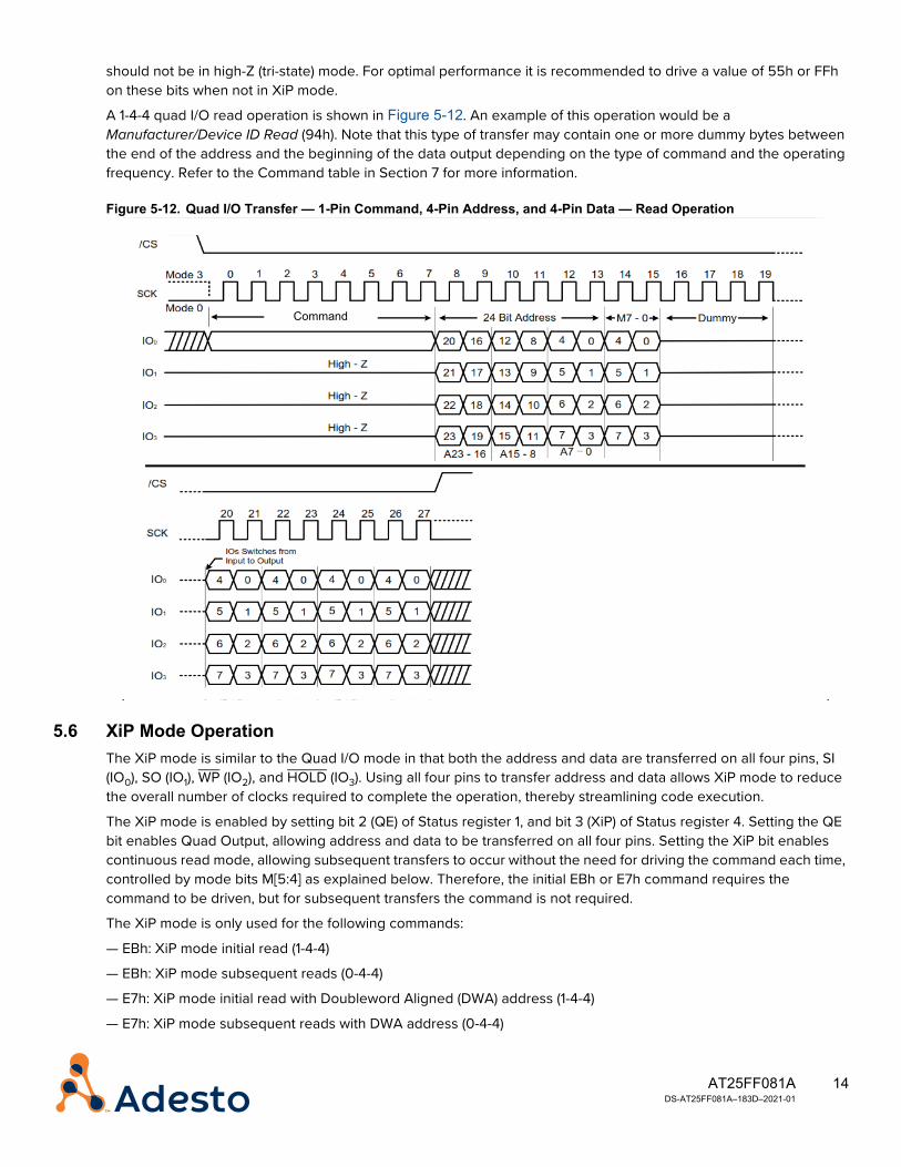
5.5 Quad I/O Operation (1-4-4)The AT25FF081A supports the Quad I/O mode which enhances overall throughput over the standard SPI and dual operation modes by increasing the data transfer rate. In this mode, address and data are transferred on four pins; SI, SO, WP, and HOLD. This means that only 1/4th the number of clocks are required to transfer the address and data relative to standard SPI mode. This is known as a 1-4-4 transfer which is defined as follows:
• 1-pin command, 4-pin address, and 4-pin data (1-4-4)
In Quad I/O mode the command (C) is driven to the memory device on the SI (IO0) pin. During write operations, the SI (IO0), SO (IO1), WP (IO2), and HOLD (IO3) pins switched to inputs and the address and data are driven on all four pins, allowing four bits to be transferred on every clock. During read operations, once the command is transferred on the SI (IO0) pin, address is transferred on the SI (IO0), SO (IO1), WP (IO2), and HOLD (IO3) pins, allowing a 24-bit address to be transferred in only six clocks. Once the address transfer is complete, these pins are switched to outputs and the data is driven on all four pins, allowing four data bits to be transferred on every clock. Note that mode bits M[7:0]
I/O0(SI)
SCK2 310
C
6 75 11014 9 342493218 414037 3833 36353431 32 8474440392 4645
COMMAND
A A A A A A AA A X X X X X X X X
Address Bits A23-A0 DUMMYDATAOUT 1
DATAOUT 2
DATAOUT 3
DATAOUT 4
DATAOUT 5
I/O1(SO)
High-impedanceD5 D1 D5 D1 D5 D1 D5 D1 D5 D1
I/O2(WP)
High-impedanceD6 D2 D6 D2 D6 D2 D6 D2 D6 D2
I/O3(HOLD) MSB MSB MSB MSB MSB
High-impedanceD7 D3 D7 D3 D7 D3 D7 D3 D7 D3
D4 D0 D4 D0 D4 D0 D4 D0 D4 D0
CS
C CC CC CC
I/O0(SI)
SCK2 310
C
6 75 11014 9 93218 414037 3833 36353431 320392
COMMAND
A A A A A A AA A
Address Bits A23-A0
I/O1(SO)
High-impedance
I/O2(WP)
High-impedance
I/O3(HOLD)
High-impedance
CS
C CC CC CC
DATA IN 1
DATA IN 2
DATA IN 3
DATA IN 4
DATA IN 5
D5 D1 D5 D1 D5 D1 D5 D1 D5 D1
D6 D2 D6 D2 D6 D2 D6 D2 D6 D2
MSB MSB MSB MSB MSB
D7 D3 D7 D3 D7 D3 D7 D3 D7 D3
D4 D0 D4 D0 D4 D0 D4 D0 D4 D0
14AT25FF081A DS-AT25FF081A–183D–2021-01
should not be in high-Z (tri-state) mode. For optimal performance it is recommended to drive a value of 55h or FFh on these bits when not in XiP mode.
A 1-4-4 quad I/O read operation is shown in Figure 5-12. An example of this operation would be a Manufacturer/Device ID Read (94h). Note that this type of transfer may contain one or more dummy bytes between the end of the address and the beginning of the data output depending on the type of command and the operating frequency. Refer to the Command table in Section 7 for more information.
Figure 5-12. Quad I/O Transfer — 1-Pin Command, 4-Pin Address, and 4-Pin Data — Read Operation
5.6 XiP Mode OperationThe XiP mode is similar to the Quad I/O mode in that both the address and data are transferred on all four pins, SI (IO0), SO (IO1), WP (IO2), and HOLD (IO3). Using all four pins to transfer address and data allows XiP mode to reduce the overall number of clocks required to complete the operation, thereby streamlining code execution.
The XiP mode is enabled by setting bit 2 (QE) of Status register 1, and bit 3 (XiP) of Status register 4. Setting the QE bit enables Quad Output, allowing address and data to be transferred on all four pins. Setting the XiP bit enables continuous read mode, allowing subsequent transfers to occur without the need for driving the command each time, controlled by mode bits M[5:4] as explained below. Therefore, the initial EBh or E7h command requires the command to be driven, but for subsequent transfers the command is not required.
The XiP mode is only used for the following commands:
— EBh: XiP mode initial read (1-4-4)
— EBh: XiP mode subsequent reads (0-4-4)
— E7h: XiP mode initial read with Doubleword Aligned (DWA) address (1-4-4)
— E7h: XiP mode subsequent reads with DWA address (0-4-4)
Command
15AT25FF081A DS-AT25FF081A–183D–2021-01
As shown above, the only difference between the EBh and E7h commands is that the E7h command is performed only on a double-word aligned address boundary. The EBh command does not have this restriction. Note that mode bits M[7:0] should not be in high-Z (tri-state) mode. For optimal performance it is recommended to drive a value of 55h or FFh on these bits when not in XiP mode.
The Set Burst with Wrap (77h) command does not access the memory directly, but rather is used in conjunction with the EBh and E7h commands to select 8-, 16-, 32-, or 64-Byte sections within a 256-byte page. The user selects the size by programming the wrap bits as part of the 77h command. Refer to the table in Section 7.13, Set Burst Wrap (77h) for more information.
When the EBh/E7h command is driven onto the bus, the associated data immediately following the address contains eight mode bits, known as M[7:0]. Of these bits, M[5:4] are decoded and used by hardware to determine if the device is in XiP continuous read mode. If the value on M[5:4] equals 2’b10, the device is placed into XiP mode to allow for continuous read operations to occur, meaning that for subsequent operations the command field is not required. Each time a subsequent transfer is made, it contains only the address and mode bits.
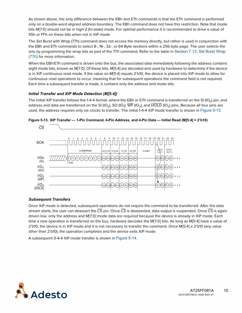
Initial Transfer and XiP Mode Detection (M[5:4])The initial XiP transfer follows the 1-4-4 format, where the EBh or E7h command is transferred on the SI (IO0) pin, and address and data are transferred on the SI (IO0), SO (IO1), WP (IO2), and HOLD (IO3) pins. Because all four pins are used, the address requires only six clocks to transfer. The initial 1-4-4 XiP mode transfer is shown in Figure 5-13.
Figure 5-13. XiP Transfer — 1-Pin Command, 4-Pin Address, and 4-Pin Data — Initial Read (M[5:4] = 2’b10)
Subsequent TransfersOnce XiP mode is detected, subsequent operations do not require the command to be transferred. After the data stream starts, the user can deassert the CS pin. Once CS is deasserted, data output is suspended. Once CS is again driven low, only the address and M[7:0] mode data are required because the device is already in XiP mode. Each time a new operation is transferred on the bus, hardware decodes the M[7:0] bits. As long as M[5:4] have a value of 2’b10, the device is in XiP mode and it is not necessary to transfer the command. Once M[5:4] ≠ 2’b10 (any value other than 2’b10), the operation completes and the device exits XiP mode.
A subsequent 0-4-4 XiP mode transfer is shown in Figure 5-14.
I/O0(SI)
SCK
I/O1(SO)
CS
MSB
2 310
C C C C C C C C
6 75 11014 9 918 17 1816
COMMAND
A20 A16 A12 A8
A23-A16 A15-A8
A21 A17 A13 A9
2321 2220
D4
D1
D0
D5
D4
DATAOUT 1
D5
D0
D1
DATAOUT 2
I/O2(WP)
A22 A18 A14 A10 D2 D6D6 D2
I/O3(HOLD)
A23 A19 A15 A11 D3 D7D7 D3
14 151312
A4 A0 M4 M0
A7-A0 M7-M0
A6 A2 M6 M2
A7 A3 M7 M3
A5 A1 M5 M1
DUMMY
16AT25FF081A DS-AT25FF081A–183D–2021-01
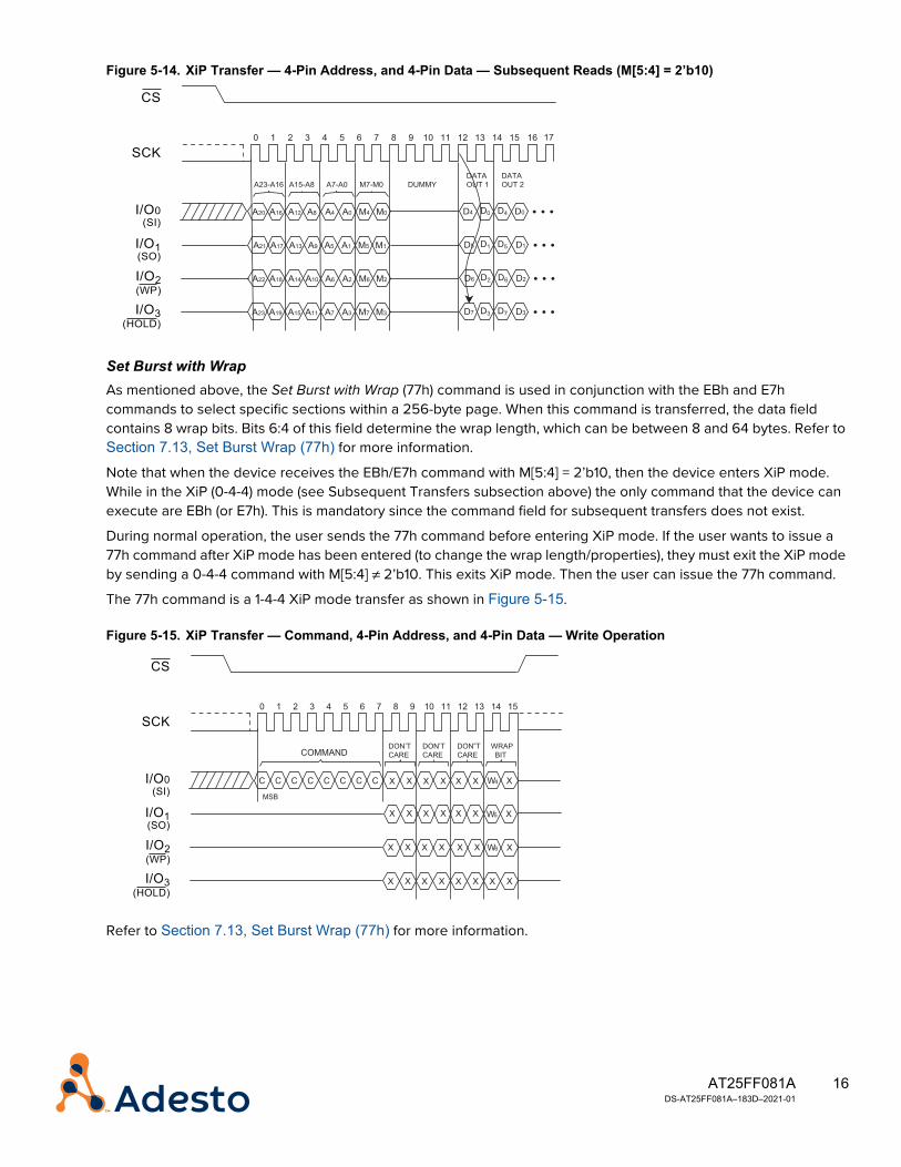
Figure 5-14. XiP Transfer — 4-Pin Address, and 4-Pin Data — Subsequent Reads (M[5:4] = 2’b10)
Set Burst with WrapAs mentioned above, the Set Burst with Wrap (77h) command is used in conjunction with the EBh and E7h commands to select specific sections within a 256-byte page. When this command is transferred, the data field contains 8 wrap bits. Bits 6:4 of this field determine the wrap length, which can be between 8 and 64 bytes. Refer to Section 7.13, Set Burst Wrap (77h) for more information.
Note that when the device receives the EBh/E7h command with M[5:4] = 2’b10, then the device enters XiP mode. While in the XiP (0-4-4) mode (see Subsequent Transfers subsection above) the only command that the device can execute are EBh (or E7h). This is mandatory since the command field for subsequent transfers does not exist.
During normal operation, the user sends the 77h command before entering XiP mode. If the user wants to issue a 77h command after XiP mode has been entered (to change the wrap length/properties), they must exit the XiP mode by sending a 0-4-4 command with M[5:4] ≠ 2’b10. This exits XiP mode. Then the user can issue the 77h command.
The 77h command is a 1-4-4 XiP mode transfer as shown in Figure 5-15.
Figure 5-15. XiP Transfer — Command, 4-Pin Address, and 4-Pin Data — Write Operation
Refer to Section 7.13, Set Burst Wrap (77h) for more information.
I/O0(SI)
SCK
I/O1(SO)
CS
2 310 6 75 11014 98 16
I/O2(WP)
I/O3(HOLD)
14 151312
A20 A16 A12 A8
A23-A16 A15-A8
A21 A17 A13 A9
D4
D1
D0
D5
D4
DATAOUT 1
D5
D0
D1
DATA OUT 2
A22 A18 A14 A10 D2 D6D6 D2
A23 A19 A15 A11 D3 D7D7 D3
A4 A0 M4 M0
A7-A0 M7-M0
A6 A2 M6 M2
A7 A3 M7 M3
A5 A1 M5 M1
DUMMY
17
I/O0(SI)
SCK
I/O1(SO)
CS
MSB
2 310
C C C C C C C C
6 75 11014 98
COMMANDDON’TCARE
DON’TCARE
I/O2(WP)
I/O3(HOLD)
14 151312
W4
DON”TCARE
WRAP BIT
W6
X
W5
X
X
X
X X X X X X X
X X X X
X X
X X X X
X X
X X
X X
X X
17AT25FF081A DS-AT25FF081A–183D–2021-01
5.7 Memory ArchitectureThe memory array of the AT25FF081A memory array is divided into three levels of granularity comprised of blocks and pages;
• 64 KB blocks
• 32 KB blocks
• 4 KB blocks
The size of the erase blocks is optimized for both code and data storage applications, allowing both code and data segments to reside in their own erase regions.
Figure 5-16 illustrates the breakdown of each level and details the number of pages per block. The program operations to the memory array can be done at the full page level or at the byte level (a variable number of bytes). Erase operations can be performed at the chip or block level.

18AT25FF081A DS-AT25FF081A–183D–2021-01
Figure 5-16. AT25FF081A Device Block Memory Map
Figure 5-17 shows how one 4 KB block maps to sixteen 256 byte pages. The very top and bottom block ranges are shown.
64 KB Block Erase (D8h) 32 KB Block Erase (52h) 4 KB Block Erase (20h) (1)
1. B = Block
Block Address Range
64 KB(block 15)
32 KB(block 31)
4 KB (B255) 0FF000h - 0FFFFFh4 KB (B254) 0FE000h - 0FEFFFh4 KB (B253) 0FD000h - 0FDFFFh4 KB (B252) 0FC000h - 0FCFFFh4 KB (B251) 0FB000h - 0FBFFFh4 KB (B250) 0FA000h - 0FAFFFh4 KB (B249) 0F9000h - 0F9FFFh4 KB (B248) 0F8000h - 0F8FFFh
32 KB(block 30)
4 KB (B247) 0F7000h - 0F7FFFh4 KB (B246) 0F6000h - 0F6FFFh4 KB (B245) 0F5000h - 0F5FFFh4 KB (B244) 0F4000h - 0F4FFFh4 KB (B243) 0F3000h - 0F3FFFh4 KB (B242) 0F2000h - 0F2FFFh4 KB (B241) 0F1000h - 0F1FFFh4 KB (B240) 0F0000h - 0F0FFFh
64 KB (block 14)to
64 KB (block 1)
32 KB (block 29)to
32 KB (block 2)
4 KB (B239)to
4 KB (B16)
0EF000h - 0EFFFFhto
010000h - 010FFFh
64 KB(block 0
32 KB(block 1)
4 KB (B15) 00F000h - 00FFFFh4 KB (B14) 00E000h - 00EFFFh4 KB (B13) 00D000h - 00DFFFh4 KB (B12) 00C000h - 00CFFFh4 KB (B11) 00B000h - 00BFFFh4 KB (B10) 00A000h - 00AFFFh4 KB (B9) 009000h - 009FFFh4 KB (B8) 008000h - 008FFFh
32 KB(block 0)
4 KB (B7) 007000h - 007FFFh4 KB (B6) 006000h - 006FFFh4 KB (B5) 005000h - 005FFFh4 KB (B4) 004000h - 004FFFh4 KB (B3) 003000h - 003FFFh4 KB (B2) 002000h - 002FFFh4 KB (B1) 001000h - 001FFFh4 KB (B0) 000000h - 000FFFh

19AT25FF081A DS-AT25FF081A–183D–2021-01
Figure 5-17. AT25FF081A Device Block Memory Map — Page Program
4 KB Blocks 256 Byte Page 1 - 256 Byte Page Program (02h)
4 KB (B255) 256 Bytes 0FFF00h - 0FFFFFh4 KB (B254) 256 Bytes 0FFE00h - 0FFEFFh4 KB (B253) 256 Bytes 0FFD00h - 0FFDFFh4 KB (B252) 256 Bytes 0FFC00h - 0FFCFFh4 KB (B251) 256 Bytes 0FFB00h - 0FFBFFh4 KB (B250) 256 Bytes 0FFA00h - 0FFAFFh4 KB (B249) 256 Bytes 0FF900h - 0FF9FFh4 KB (B248) 256 Bytes 0FF800h - 0FF8FFh4 KB (B247) 256 Bytes 0FF700h - 0FF7FFh4 KB (B246) 256 Bytes 0FF600h - 0FF6FFh4 KB (B245) 256 Bytes 0FF500h - 0FF5FFh4 KB (B244) 256 Bytes 0FF400h - 0FF4FFh4 KB (B243) 256 Bytes 0FF300h - 0FF3FFh4 KB (B242) 256 Bytes 0FF200h - 0FF2FFh4 KB (B241) 256 Bytes 0FF100h - 0FF1FFh4 KB (B240) 256 Bytes 0FF000h - 0FF0FFh4KB (B239)
to4KB (B16)
.
.
.
.
.
.
.
.
.4 KB (B15) 256 Bytes 000F00h - 000FFFh4 KB (B14) 256 Bytes 000E00h - 000EFFh4 KB (B13) 256 Bytes 000D00h - 000DFFh4 KB (B12) 256 Bytes 000C00h - 000CFFh4 KB (B11) 256 Bytes 000B00h - 000BFFh4 KB (B10) 256 Bytes 000A00h - 000AFFh4 KB (B9) 256 Bytes 000900h - 0009FFh4 KB (B8) 256 Bytes 000800h - 0008FFh4 KB (B7) 256 Bytes 000700h - 0007FFh4 KB (B6) 256 Bytes 000600h - 0006FFh4 KB (B5) 256 Bytes 000500h - 0005FFh4 KB (B4) 256 Bytes 000400h - 0004FFh4 KB (B3) 256 Bytes 000300h - 0003FFh4 KB (B2) 256 Bytes 000200h - 0002FFh4 KB (B1) 256 Bytes 000100h - 0001FFh4 KB (B0) 256 Bytes 000000h - 0000FFh
20AT25FF081A DS-AT25FF081A–183D–2021-01
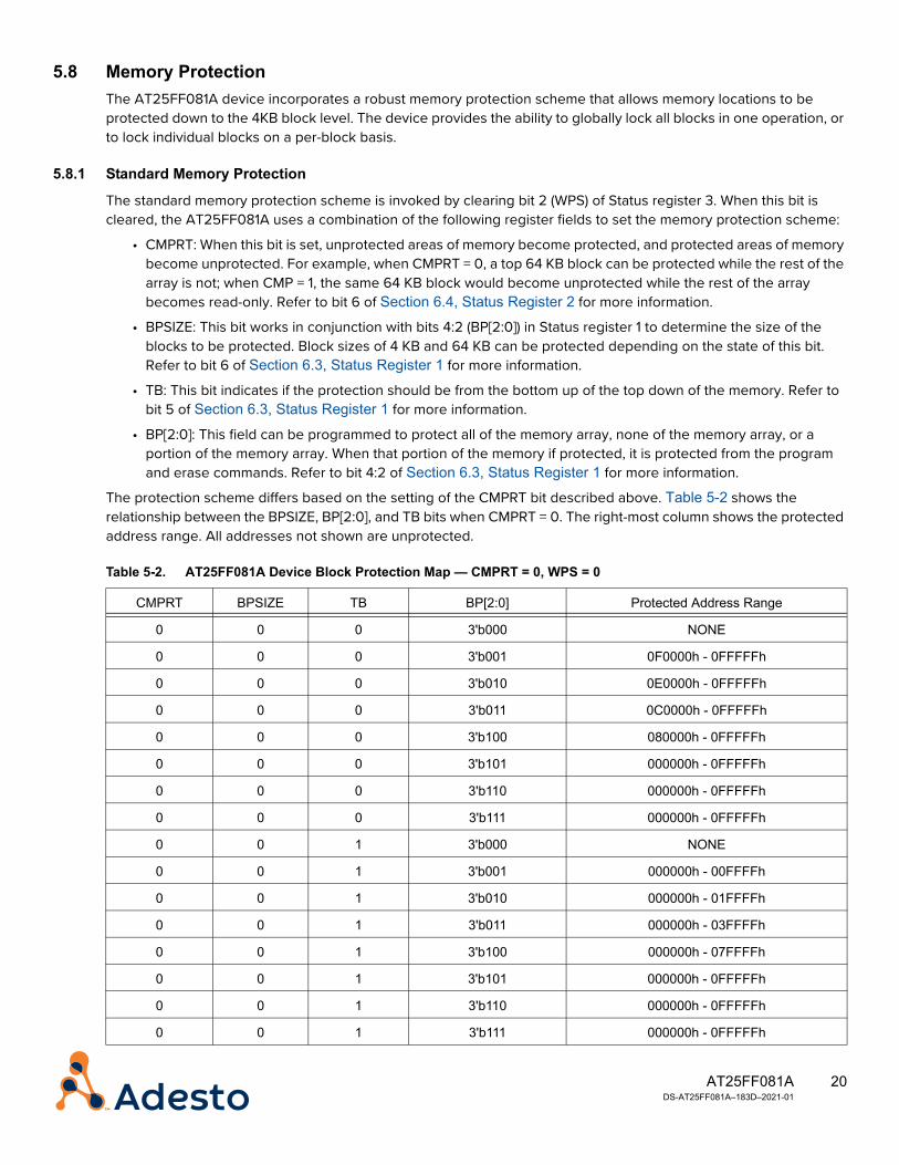
5.8 Memory ProtectionThe AT25FF081A device incorporates a robust memory protection scheme that allows memory locations to be protected down to the 4KB block level. The device provides the ability to globally lock all blocks in one operation, or to lock individual blocks on a per-block basis.
5.8.1 Standard Memory Protection
The standard memory protection scheme is invoked by clearing bit 2 (WPS) of Status register 3. When this bit is cleared, the AT25FF081A uses a combination of the following register fields to set the memory protection scheme:
• CMPRT: When this bit is set, unprotected areas of memory become protected, and protected areas of memory become unprotected. For example, when CMPRT = 0, a top 64 KB block can be protected while the rest of the array is not; when CMP = 1, the same 64 KB block would become unprotected while the rest of the array becomes read-only. Refer to bit 6 of Section 6.4, Status Register 2 for more information.
• BPSIZE: This bit works in conjunction with bits 4:2 (BP[2:0]) in Status register 1 to determine the size of the blocks to be protected. Block sizes of 4 KB and 64 KB can be protected depending on the state of this bit. Refer to bit 6 of Section 6.3, Status Register 1 for more information.
• TB: This bit indicates if the protection should be from the bottom up of the top down of the memory. Refer to bit 5 of Section 6.3, Status Register 1 for more information.
• BP[2:0]: This field can be programmed to protect all of the memory array, none of the memory array, or a portion of the memory array. When that portion of the memory if protected, it is protected from the program and erase commands. Refer to bit 4:2 of Section 6.3, Status Register 1 for more information.
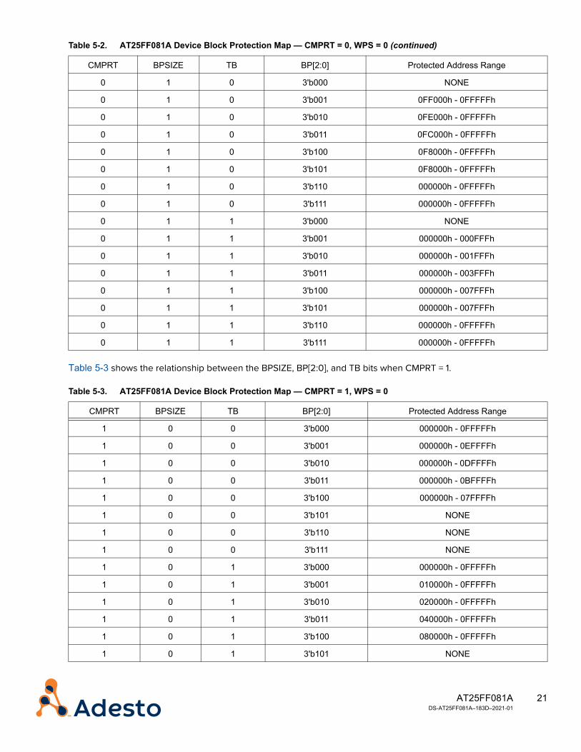
The protection scheme differs based on the setting of the CMPRT bit described above. Table 5-2 shows the relationship between the BPSIZE, BP[2:0], and TB bits when CMPRT = 0. The right-most column shows the protected address range. All addresses not shown are unprotected.
Table 5-2. AT25FF081A Device Block Protection Map — CMPRT = 0, WPS = 0
CMPRT BPSIZE TB BP[2:0] Protected Address Range
0 0 0 3'b000 NONE
0 0 0 3'b001 0F0000h - 0FFFFFh
0 0 0 3'b010 0E0000h - 0FFFFFh
0 0 0 3'b011 0C0000h - 0FFFFFh
0 0 0 3'b100 080000h - 0FFFFFh
0 0 0 3'b101 000000h - 0FFFFFh
0 0 0 3'b110 000000h - 0FFFFFh
0 0 0 3'b111 000000h - 0FFFFFh
0 0 1 3'b000 NONE
0 0 1 3'b001 000000h - 00FFFFh
0 0 1 3'b010 000000h - 01FFFFh
0 0 1 3'b011 000000h - 03FFFFh
0 0 1 3'b100 000000h - 07FFFFh
0 0 1 3'b101 000000h - 0FFFFFh
0 0 1 3'b110 000000h - 0FFFFFh
0 0 1 3'b111 000000h - 0FFFFFh
21AT25FF081A DS-AT25FF081A–183D–2021-01
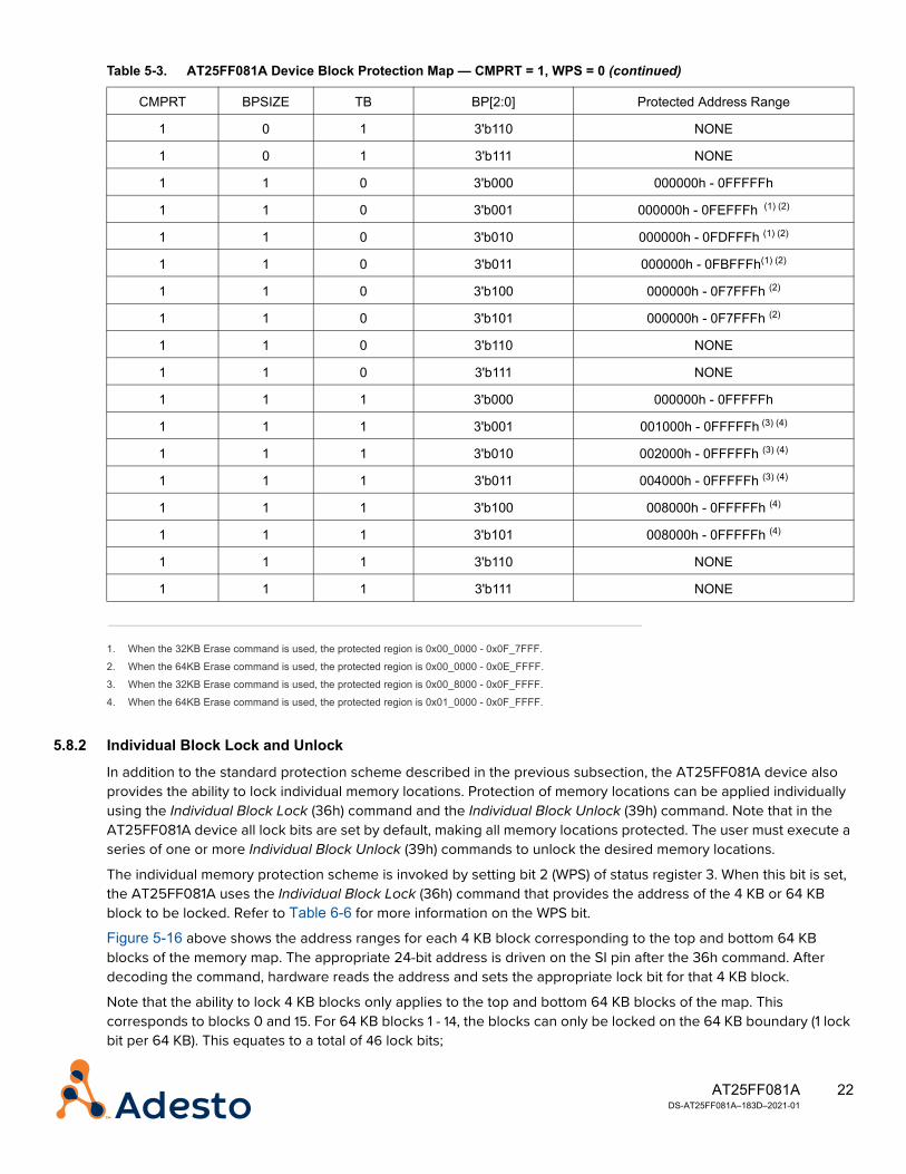
Table 5-3 shows the relationship between the BPSIZE, BP[2:0], and TB bits when CMPRT = 1.
0 1 0 3'b000 NONE
0 1 0 3'b001 0FF000h - 0FFFFFh
0 1 0 3'b010 0FE000h - 0FFFFFh
0 1 0 3'b011 0FC000h - 0FFFFFh
0 1 0 3'b100 0F8000h - 0FFFFFh
0 1 0 3'b101 0F8000h - 0FFFFFh
0 1 0 3'b110 000000h - 0FFFFFh
0 1 0 3'b111 000000h - 0FFFFFh
0 1 1 3'b000 NONE
0 1 1 3'b001 000000h - 000FFFh
0 1 1 3'b010 000000h - 001FFFh
0 1 1 3'b011 000000h - 003FFFh
0 1 1 3'b100 000000h - 007FFFh
0 1 1 3'b101 000000h - 007FFFh
0 1 1 3'b110 000000h - 0FFFFFh
0 1 1 3'b111 000000h - 0FFFFFh
Table 5-3. AT25FF081A Device Block Protection Map — CMPRT = 1, WPS = 0
CMPRT BPSIZE TB BP[2:0] Protected Address Range
1 0 0 3'b000 000000h - 0FFFFFh
1 0 0 3'b001 000000h - 0EFFFFh
1 0 0 3'b010 000000h - 0DFFFFh
1 0 0 3'b011 000000h - 0BFFFFh
1 0 0 3'b100 000000h - 07FFFFh
1 0 0 3'b101 NONE
1 0 0 3'b110 NONE
1 0 0 3'b111 NONE
1 0 1 3'b000 000000h - 0FFFFFh
1 0 1 3'b001 010000h - 0FFFFFh
1 0 1 3'b010 020000h - 0FFFFFh
1 0 1 3'b011 040000h - 0FFFFFh
1 0 1 3'b100 080000h - 0FFFFFh
1 0 1 3'b101 NONE
Table 5-2. AT25FF081A Device Block Protection Map — CMPRT = 0, WPS = 0 (continued)
CMPRT BPSIZE TB BP[2:0] Protected Address Range
22AT25FF081A DS-AT25FF081A–183D–2021-01
5.8.2 Individual Block Lock and Unlock
In addition to the standard protection scheme described in the previous subsection, the AT25FF081A device also provides the ability to lock individual memory locations. Protection of memory locations can be applied individually using the Individual Block Lock (36h) command and the Individual Block Unlock (39h) command. Note that in the AT25FF081A device all lock bits are set by default, making all memory locations protected. The user must execute a series of one or more Individual Block Unlock (39h) commands to unlock the desired memory locations.
The individual memory protection scheme is invoked by setting bit 2 (WPS) of status register 3. When this bit is set, the AT25FF081A uses the Individual Block Lock (36h) command that provides the address of the 4 KB or 64 KB block to be locked. Refer to Table 6-6 for more information on the WPS bit.
Figure 5-16 above shows the address ranges for each 4 KB block corresponding to the top and bottom 64 KB blocks of the memory map. The appropriate 24-bit address is driven on the SI pin after the 36h command. After decoding the command, hardware reads the address and sets the appropriate lock bit for that 4 KB block.
Note that the ability to lock 4 KB blocks only applies to the top and bottom 64 KB blocks of the map. This corresponds to blocks 0 and 15. For 64 KB blocks 1 - 14, the blocks can only be locked on the 64 KB boundary (1 lock bit per 64 KB). This equates to a total of 46 lock bits;
1 0 1 3'b110 NONE
1 0 1 3'b111 NONE
1 1 0 3'b000 000000h - 0FFFFFh
1 1 0 3'b001 000000h - 0FEFFFh (1) (2)
1 1 0 3'b010 000000h - 0FDFFFh (1) (2)
1 1 0 3'b011 000000h - 0FBFFFh(1) (2)
1 1 0 3'b100 000000h - 0F7FFFh (2)
1 1 0 3'b101 000000h - 0F7FFFh (2)
1 1 0 3'b110 NONE
1 1 0 3'b111 NONE
1 1 1 3'b000 000000h - 0FFFFFh
1 1 1 3'b001 001000h - 0FFFFFh (3) (4)
1 1 1 3'b010 002000h - 0FFFFFh (3) (4)
1 1 1 3'b011 004000h - 0FFFFFh (3) (4)
1 1 1 3'b100 008000h - 0FFFFFh (4)
1 1 1 3'b101 008000h - 0FFFFFh (4)
1 1 1 3'b110 NONE
1 1 1 3'b111 NONE
1. When the 32KB Erase command is used, the protected region is 0x00_0000 - 0x0F_7FFF.
2. When the 64KB Erase command is used, the protected region is 0x00_0000 - 0x0E_FFFF.
3. When the 32KB Erase command is used, the protected region is 0x00_8000 - 0x0F_FFFF.
4. When the 64KB Erase command is used, the protected region is 0x01_0000 - 0x0F_FFFF.
Table 5-3. AT25FF081A Device Block Protection Map — CMPRT = 1, WPS = 0 (continued)
CMPRT BPSIZE TB BP[2:0] Protected Address Range
23AT25FF081A DS-AT25FF081A–183D–2021-01
• 16 bits, one per 4 KB sub-block in the top 64 KB block
• 16 bits, one per 4 KB sub-block in the bottom 64 KB block
• 14 bits, one each for 64 KB blocks 1 - 14
Refer to Section 7.17, Individual Block Lock (36h) and Section 7.18, Individual Block Unlock (39h) for more information.
5.8.3 Global Block Lock and Unlock
In addition to individual block protection of memory locations as described in the previous subsection, the AT25FF081A also allows for the blocks to be locked and unlocked globally using the Global Block Lock (7Eh) and the Global Block Unlock (98h) commands. Note that in the AT25FF081A device all lock bits are set by default, making all memory locations protected. The user must execute a Global Unlock Block command to unlock the memory locations.
Refer to Section 7.20, Global Block Lock (7Eh) and Section 7.21, Global Block Unlock (98h) for more information.
5.8.4 Reading the State of the Lock Bits
In addition to globally or individually locking and unlocking selected memory blocks as described above, the AT25FF081A device allows the user to poll any block in memory to determine if it has been locked. This is accomplished by executing either the 3Ch or 3Dh command, along with the 24-bit address. Both of these commands perform the exact same operation and can be used interchangeably.
Once this information is decoded, hardware fetches the 8-bit lock field from the requested location and outputs this information onto the SO pin. The most significant bit (MSB) of the value is transferred first, and the least significant bit (LSB) is transferred last. If the LSB is 1, the corresponding block is locked and no erase or program operation can be executed to that block. If the LSB is 0, the block or section is unlocked and program/erase operations are allowed. Refer to Section 7.19, Read Block Lock (3Ch/3Dh) for more information.
5.9 Power Down ConsiderationsThe AT25FF081A device supports the Deep Power Down (B9h) and Ultra Deep Power Down (79h/B9h) modes. In addition, bit 7 (PDM) of Status register 4 (SR4) can be used to select either of these modes using the B9h command. The 79h command is provided for backward compatibility.
There are three ways to enter power down mode:1. Set the PDM bit in SR4 (logic 1) and execute the B9h command to place the device into Deep Power Down
(DPD) mode. In this mode it is possible to execute the Resume from Power Down (ABh) command or Enable Reset (66h) and Reset Device (99h) commands in order to exit DPD mode. The device could also be reset by JEDEC reset, hardware reset, or power-on-reset in order to exit DPD mode. The exit from DPD mode time is defined by the tRDPD timing parameter in the AC specifications section of this document. Refer to Section 5.9.2 below. Note that in the AT25FF081A device, simply deasserting CS as in other devices does not exit DPD mode.
2. Clear the PDM bit in SR4 (logic 0) and execute the B9h command to place the device into Ultra Deep Power Down (UDPD) mode. To exit this mode, it is necessary to execute the Resume from Ultra-Deep Power Down (ABh) command or a JEDEC reset, hardware reset, or power-on-reset to initiate an internal reset of the device. The resume from UDPD mode recovery time is defined by the tRUDPD timing parameter in the AC specifications section of this document. Refer to Section 5.9.2 below. Note that in the AT25FF081A device, simply deasserting CS as in other devices does NOT exit UDPD mode.
3. Execute the 79h command to place the device into Ultra Deep Power Down (UDPD) mode. If this command is used, the state of the PDM bit in SR4 is ignored. This mode allows for software backward compatibility. A device reset is required to exit UPDP mode. In this mode it is necessary to execute the Resume from Ultra-Deep Power Down (ABh) command or a JEDEC reset, hardware reset or power-on-reset to initiate an internal
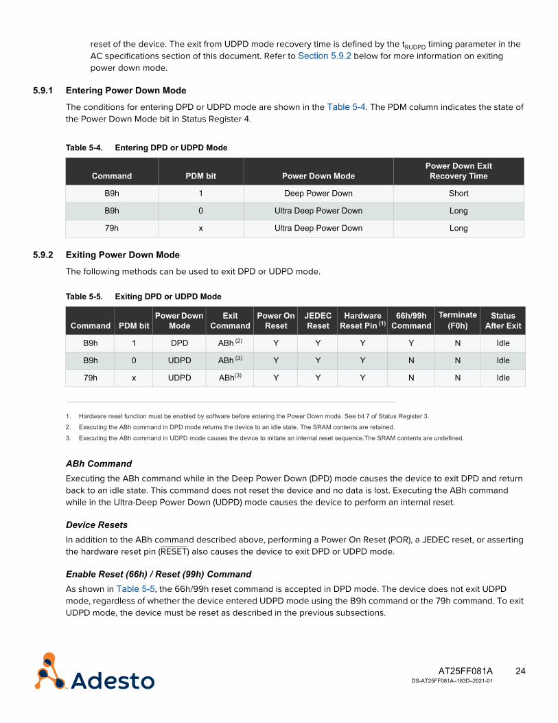
24AT25FF081A DS-AT25FF081A–183D–2021-01
reset of the device. The exit from UDPD mode recovery time is defined by the tRUDPD timing parameter in the AC specifications section of this document. Refer to Section 5.9.2 below for more information on exiting power down mode.
5.9.1 Entering Power Down Mode
The conditions for entering DPD or UDPD mode are shown in the Table 5-4. The PDM column indicates the state of the Power Down Mode bit in Status Register 4.
5.9.2 Exiting Power Down Mode
The following methods can be used to exit DPD or UDPD mode.
ABh CommandExecuting the ABh command while in the Deep Power Down (DPD) mode causes the device to exit DPD and return back to an idle state. This command does not reset the device and no data is lost. Executing the ABh command while in the Ultra-Deep Power Down (UDPD) mode causes the device to perform an internal reset.
Device ResetsIn addition to the ABh command described above, performing a Power On Reset (POR), a JEDEC reset, or asserting the hardware reset pin (RESET) also causes the device to exit DPD or UDPD mode.
Enable Reset (66h) / Reset (99h) CommandAs shown in Table 5-5, the 66h/99h reset command is accepted in DPD mode. The device does not exit UDPD mode, regardless of whether the device entered UDPD mode using the B9h command or the 79h command. To exit UDPD mode, the device must be reset as described in the previous subsections.
Table 5-4. Entering DPD or UDPD Mode
Command PDM bit Power Down ModePower Down Exit Recovery Time
B9h 1 Deep Power Down Short
B9h 0 Ultra Deep Power Down Long
79h x Ultra Deep Power Down Long
Table 5-5. Exiting DPD or UDPD Mode
Command PDM bitPower Down
ModeExit
CommandPower On
ResetJEDEC Reset
Hardware Reset Pin (1)
1. Hardware reset function must be enabled by software before entering the Power Down mode. See bit 7 of Status Register 3.
66h/99h Command
Terminate(F0h)
Status After Exit
B9h 1 DPD ABh (2)
2. Executing the ABh command in DPD mode returns the device to an idle state. The SRAM contents are retained.
Y Y Y Y N Idle
B9h 0 UDPD ABh (3)
3. Executing the ABh command in UDPD mode causes the device to initiate an internal reset sequence.The SRAM contents are undefined.
Y Y Y N N Idle
79h x UDPD ABh(3) Y Y Y N N Idle
25AT25FF081A DS-AT25FF081A–183D–2021-01
Terminate Command (F0h)The Terminate (F0) command does not cause exit from DPD or UDPD modes. To exit DPD or UDPD mode still requires either the ABh command, or resetting the device as described in the previous subsections.
5.9.3 Reset During Program and Erase Commands
The AT25FF081A device supports the following program and erase operations.
Program operations include:
• Byte/Page Program (02h)
• Sequential Program (AFh/ADh)
• Dual Output Byte/Page Program (A2h)
• Quad Output Byte/Page Program (32h)
• Program Security Register (9Bh)
Erase operations include:
• 4KB Block Erase (20h)
• 32KB Block Erase (52h)
• 64KB Block Erase (D8h)
• Chip Erase (60h/C7h)
These commands are affected when resetting the device as shown in Table 5-6. In this table, a ‘Y’ entry indicates that the device is reset when that type of reset occurs during the corresponding command. A ‘N’ entry indicates that the operation is terminated, but the device is not reset. For example, when the F0h command is executed during a program or erase operation, the operation is halted, but the device is not reset.
5.10 Erase/Program Suspend Considerations and Nested OperationsThe AT25FF081A device provides three status register bits to manage program and erase suspend operations.
• SUSP — Status Register 2, bit 7. The SUSP bit is set by hardware and indicates that the program or erase operation has been suspended.
• ES — Status Register 5, bit 3. The ES bit is set by hardware whenever an erase operation is suspended.
• PS — Status Register 5, bit 2. The PS bit is set by hardware whenever a program operation is suspended.
These three bits work in conjunction to define the state of a suspend operation as shown in Table 5-7.
In this table, the SUSP is a logical OR of the ES and PS bits. When either the ES or PS bit is set, the SUSP bit is set. When both of the ES and PS bits are cleared, the SUSP bit is cleared.
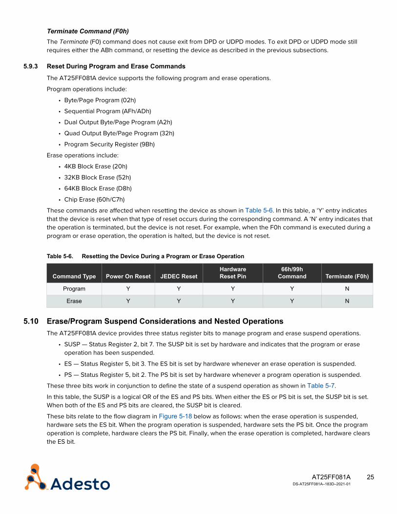
These bits relate to the flow diagram in Figure 5-18 below as follows: when the erase operation is suspended, hardware sets the ES bit. When the program operation is suspended, hardware sets the PS bit. Once the program operation is complete, hardware clears the PS bit. Finally, when the erase operation is completed, hardware clears the ES bit.
Table 5-6. Resetting the Device During a Program or Erase Operation
Command Type Power On Reset JEDEC ResetHardware Reset Pin
66h/99h Command Terminate (F0h)
Program Y Y Y Y N
Erase Y Y Y Y N
26AT25FF081A DS-AT25FF081A–183D–2021-01
5.10.1 Nested Operations
The AT25FF081A device supports nested erase and program suspend operations. An erase operation can be suspended and a program operation started. This operation can then also be suspended and another operation commenced, such as a read. After the read operation is complete, the program operation can be resumed. Once the program operation is completed, the erase operation can be resumed. Nested operations adhere to the following constraint:
• Suspending an erase operation followed by a program operation is supported
• Suspending a program operation followed by an erase operation is NOT supported
The erase operation must be suspended first, followed by suspension of the program operation.
Figure 5-18 shows an example flow diagram of a nested operation.
Table 5-7. Encoding of Erase/Program Suspend Operations
SUSP ES PS Status
0 0 0 No suspend operation in progress.
1 0 1 Program suspend operation in progress.
1 1 0 Erase suspend operation in progress.
1 1 1 Nested erase/program suspend operation in progress.
27AT25FF081A DS-AT25FF081A–183D–2021-01
Figure 5-18. Flow Diagram of Nested Operations Example
5.10.2 Program and Erase Errors
The AT25FF081A device provides two Status register bits to indicate program and erase errors.
• EE — Status Register 4, bit 4. The EE bit is set by hardware whenever an error occurs during an erase operation
28AT25FF081A DS-AT25FF081A–183D–2021-01
• PE — Status Register 4, bit 5. The PE bit is set by hardware whenever an error occurs during a program operation
When a new program or erase command is accepted by the device, hardware clears the EE or PE bits respectively depending on the command. The device clears the EE bit when a new Block Erase or Chip Erase command is accepted. The device clears the PE bit when a new Byte/Page Program, Sequential Programming, Program OTP Security Register, Write Status Register, or Status Register Lock command is accepted. If an error is detected during the command execution, then the EE or PE flag is set. These flags hold their contents even if the program/erase operation is suspended. Note that the Resume command does not change the state of the EE and PE bits. If a Terminate command is issued while the device is busy (executing program/erase), then the PE or EE flag is set.
The PE and EE bits are volatile, meaning that any reset operation clears these bits. The ABh command is used to exit Deep Power Down (DPD) or Ultra-Deep Power Down (UDPD) mode. If the device is in DPD mode and the user issues the ABh command, then the device exits DPD mode but does not change the state of the PE and EE bits. However, if the ABh command is executed and the device exits from UDPD mode, then the device initiates a reset, which causes both the PE and EE bits to be cleared.
When an error occurs during a given command, the EE and PE bits are set as shown in Table 5-8. Note that for any of the commands where a ‘Yes’ appears in the EE or PE columns, when a new command is issued, the EE or PE bit is cleared. Therefore, when the bit is set initially due to an error being detected, it is incumbent on software to detect when these bits are set and take the necessary steps to determine the exact error.
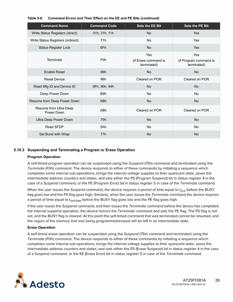
Table 5-8. Command Errors and Their Effect on the EE and PE Bits
Command Name Command Code Sets the EE Bit Sets the PE Bit
Read Array 03h, 3Bh, 6Bh, EBh, E7h No No
Block Erase 20h, 52h, D8h Yes No
Chip Erase 60h, C7h Yes No
Byte/Page Program 02h, A2h, 32h No Yes
Sequential Programming ADh, AFh No Yes
Program/Erase Suspend B0h, 75h No No
Program/Erase Resume D0h, 7Ah No No
Write Enable 06h No No
Write Disable 04h No No
Volatile Write Enable 50h No No
Individual Block Lock 36h No No
Individual Block Unlock 39h No No
Global Block Lock 7Eh No No
Global Block Unlock 98h No No
Read Block Lock Status 3Ch, 3Dh No No
Program OTP Security Register 9Bh No Yes
Read OTP Security Register 4Bh No No
Read Status Registers (direct) 05h, 35h, 15h No No
Read Status Registers (indirect) 65h No No
29AT25FF081A DS-AT25FF081A–183D–2021-01
5.10.3 Suspending and Terminating a Program or Erase Operation
Program Operation
A self-timed program operation can be suspended using the Suspend (75h) command and terminated using the Terminate (F0h) command. The device responds to either of these commands by initiating a sequence which completes some internal sub-operations, brings the internal voltage supplies to their quiescent state, saves the intermediate address counters and states, and sets either the PS (Program Suspend) bit in status register 4 in the case of a Suspend command, or the PE (Program Error) bit in status register 5 in case of the Terminate command.
When the user issues the Suspend command, the device requires a period of time equal to tSUS before the BUSY flag goes low and the PS flag goes high. Similarly, when the user issues the Terminate command the device requires a period of time equal to tSWTERM before the BUSY flag goes low and the PE flag goes high.
If the user issues the Suspend command, and then issues the Terminate command before the device has completed the internal suspend operation, the device honors the Terminate command and sets the PE flag. The PS flag is not set, and the BUSY flag is cleared. At this point the self-timed command that was terminated cannot be resumed, and the region of the memory that was being programmed/erased will be left in an intermediate state.
Erase Operation
A self-timed erase operation can be suspended using the Suspend (75h) command and terminated using the Terminate (F0h) command. The device responds to either of these commands by initiating a sequence which completes some internal sub-operations, brings the internal voltage supplies to their quiescent state, saves the intermediate address counters and states, and sets either the ES (Erase Suspend) bit in status register 4 in the case of a Suspend command, or the EE (Erase Error) bit in status register 5 in case of the Terminate command.
Write Status Registers (direct) 01h, 31h, 11h No Yes
Write Status Registers (indirect) 71h No Yes
Status Register Lock 6Fh No Yes
Terminate F0hYes
(if Erase command is terminated)
Yes(if Program command is
terminated)
Enable Reset 66h No No
Reset Device 99h Cleared on POR Cleared on POR
Read Mfg ID and Device ID 9Fh, 90h, 94h No No
Deep Power Down B9h No No
Resume from Deep Power Down ABh No No
Resume from Ultra Deep Power Down ABh Cleared on POR Cleared on POR
Ultra Deep Power Down 79h No No
Read SFDP 5Ah No No
Set Burst with Wrap 77h No No
Table 5-8. Command Errors and Their Effect on the EE and PE Bits (continued)
Command Name Command Code Sets the EE Bit Sets the PE Bit
30AT25FF081A DS-AT25FF081A–183D–2021-01
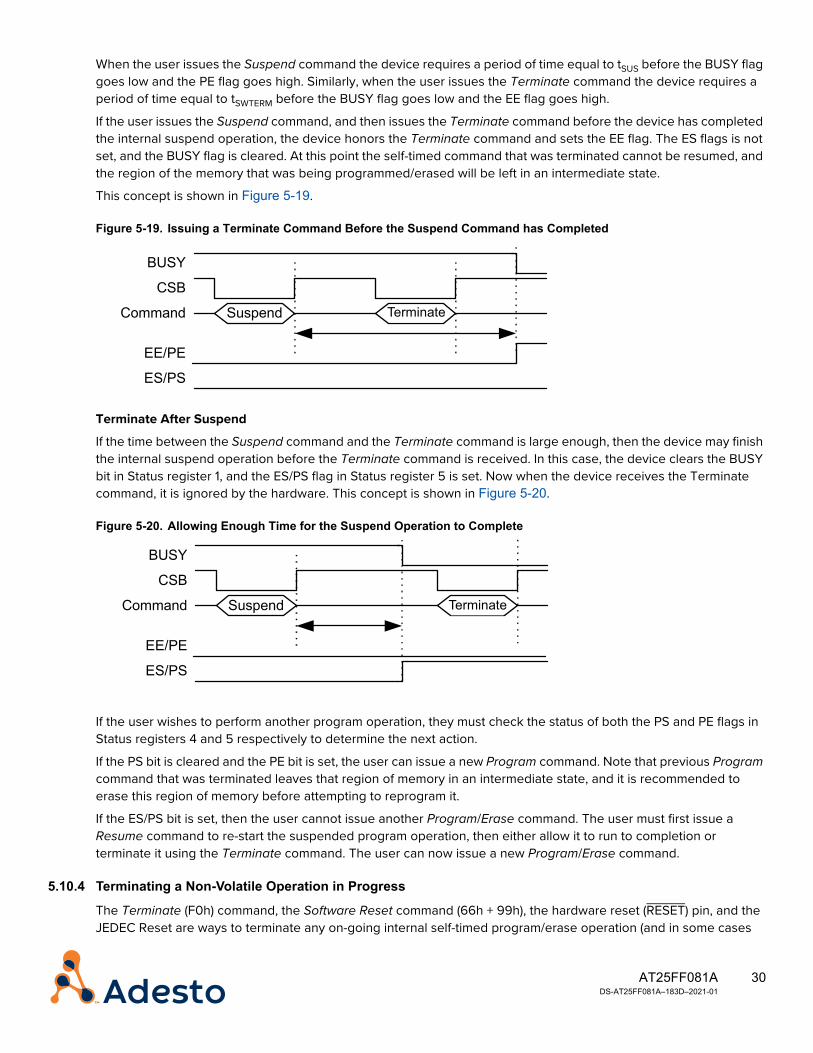
When the user issues the Suspend command the device requires a period of time equal to tSUS before the BUSY flag goes low and the PE flag goes high. Similarly, when the user issues the Terminate command the device requires a period of time equal to tSWTERM before the BUSY flag goes low and the EE flag goes high.
If the user issues the Suspend command, and then issues the Terminate command before the device has completed the internal suspend operation, the device honors the Terminate command and sets the EE flag. The ES flags is not set, and the BUSY flag is cleared. At this point the self-timed command that was terminated cannot be resumed, and the region of the memory that was being programmed/erased will be left in an intermediate state.
This concept is shown in Figure 5-19.
Figure 5-19. Issuing a Terminate Command Before the Suspend Command has Completed
Terminate After Suspend
If the time between the Suspend command and the Terminate command is large enough, then the device may finish the internal suspend operation before the Terminate command is received. In this case, the device clears the BUSY bit in Status register 1, and the ES/PS flag in Status register 5 is set. Now when the device receives the Terminate command, it is ignored by the hardware. This concept is shown in Figure 5-20.
Figure 5-20. Allowing Enough Time for the Suspend Operation to Complete
If the user wishes to perform another program operation, they must check the status of both the PS and PE flags in Status registers 4 and 5 respectively to determine the next action.
If the PS bit is cleared and the PE bit is set, the user can issue a new Program command. Note that previous Program command that was terminated leaves that region of memory in an intermediate state, and it is recommended to erase this region of memory before attempting to reprogram it.
If the ES/PS bit is set, then the user cannot issue another Program/Erase command. The user must first issue a Resume command to re-start the suspended program operation, then either allow it to run to completion or terminate it using the Terminate command. The user can now issue a new Program/Erase command.
5.10.4 Terminating a Non-Volatile Operation in Progress
The Terminate (F0h) command, the Software Reset command (66h + 99h), the hardware reset (RESET) pin, and the JEDEC Reset are ways to terminate any on-going internal self-timed program/erase operation (and in some cases
Suspend Stop
BUSY
CSB
Command
EE/PE
ES/PS
Terminate
Suspend Stop
BUSY
CSB
Command
EE/PE
ES/PS
Terminate
31AT25FF081A DS-AT25FF081A–183D–2021-01
reset the device). However, abruptly terminating a Status Register Write, Status Register Lock, or OTP Security Register Program command is not desirable as this may leave these non-volatile registers in an indeterminate state.
Therefore when the device is busy executing the Status Register Write, the Status Register Lock or the OTP Security Register Program command, then the Terminate command is ignored. The software reset, hardware reset, and JEDEC reset actions are delayed until after the internal self-timed operations are completed; once the internal operation is completed the device will be reset. Refer to Section 5.12 for more information on how to perform a JEDEC hardware reset.
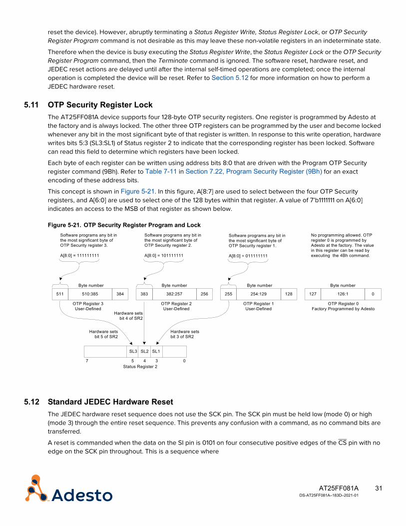
5.11 OTP Security Register LockThe AT25FF081A device supports four 128-byte OTP security registers. One register is programmed by Adesto at the factory and is always locked. The other three OTP registers can be programmed by the user and become locked whenever any bit in the most significant byte of that register is written. In response to this write operation, hardware writes bits 5:3 (SL3:SL1) of Status register 2 to indicate that the corresponding register has been locked. Software can read this field to determine which registers have been locked.
Each byte of each register can be written using address bits 8:0 that are driven with the Program OTP Security register command (9Bh). Refer to Table 7-11 in Section 7.22, Program Security Register (9Bh) for an exact encoding of these address bits.
This concept is shown in Figure 5-21. In this figure, A[8:7] are used to select between the four OTP Security registers, and A[6:0] are used to select one of the 128 bytes within that register. A value of 7’b1111111 on A[6:0] indicates an access to the MSB of that register as shown below.
Figure 5-21. OTP Security Register Program and Lock
5.12 Standard JEDEC Hardware ResetThe JEDEC hardware reset sequence does not use the SCK pin. The SCK pin must be held low (mode 0) or high (mode 3) through the entire reset sequence. This prevents any confusion with a command, as no command bits are transferred.
A reset is commanded when the data on the SI pin is 0101 on four consecutive positive edges of the CS pin with no edge on the SCK pin throughout. This is a sequence where
511 510:385 384 383 382:257 256 255 254:129 128 127 126:1 0
OTP Register 3User-Defined
Software programs any bit in the most significant byte of OTP Security register 3.
A[8:0] = 111111111
Software programs any bit in the most significant byte of OTP Security register 2.
A[8:0] = 101111111
Software programs any bit in the most significant byte of OTP Security register 1.
A[8:0] = 011111111
No programming allowed. OTP register 0 is programmed by Adesto at the factory. The value in this register can be read by executing the 4Bh command.
OTP Register 2User-Defined
OTP Register 1User-Defined
OTP Register 0Factory Programmed by Adesto
Byte numberByte number Byte number Byte number
5 4 37 0
SL3 SL2 SL1
Status Register 2
Hardware sets bit 5 of SR2
Hardware sets bit 4 of SR2
Hardware sets bit 3 of SR2

32AT25FF081A DS-AT25FF081A–183D–2021-01
1. CS is driven active low to select the device2. Clock (SCK) remains stable in either a high or low state 3. SI is driven low by the bus master, simultaneously with CS going active low. No SPI bus slave drives SI during
CS low before a transition of SCK4. CS is driven inactive. The slave captures the state of SI on the rising edge of CS
The above steps are repeated 4 times, each time alternating the state of SI.
After the fourth CS pulse, the slave triggers its internal reset. SI is low on the first CS, high on the second, low on the third, high on the fourth. This provides a value of 5h, unlike random noise. Any activity on SCK during this time halts the sequence and a Reset will not be generated.
After a JEDEC hardware reset while the device is in Ultra-Deep Power Down (UDPD) mode, the SRAM buffer resets to an undefined value. Hardware resets all volatile status registers, including the block protection bits, to their default values.
After a JEDEC hardware reset while the device is in any other mode than UDPD mode, the SRAM buffer keeps the values it had prior to Reset, with the following exception: If the reset sequence is initiated during an update of the SRAM buffer, the contents of the SRAM buffer may be corrupted. Hardware resets all volatile status registers, including the block protection bits, reset to their default values.
All non-volatile status registers keep the value they had prior to reset, with the following exception: If the reset sequence is initiated during a write to a non-volatile status register, the value of that register may be corrupted.
The device will always revert back to standard SPI mode after JEDEC hardware reset. Figure 5-22 below illustrates the timing for the JEDEC hardware reset operation.
Figure 5-22. JEDEC Standard Hardware Reset
5.13 Chip Select RestrictionsThe CS pin is used to start and end operations in the device. Once the CS pin is asserted and the operation begins, it can only be deasserted on a byte boundary. If the CS pin is deasserted on a non-byte boundary, the operation is ignored.
For example, when executing the ABh command to exit power down mode, only the command is required. No address and data are required to perform this operation. Therefore, only eight clocks are required to transfer the command. If the CS pin is raised after the 8th clock (most significant bit of the command is transferred), hardware performs the operation. If the CS pin is raised after the 9th or 10th clock (not a byte boundary), the operation is ignored and no ABh command is executed.
Similarly, if the ABh command is used to fetch the device ID, once the CS pin is asserted, 40 clock cycles are required: 8 clocks for the command, 24 dummy clocks, and 8 clocks to shift out the device ID. If the CS pin is raised after the 40th clock, hardware transfers the ID information, exits power down mode, and completes the operation.
tRUDPD
33AT25FF081A DS-AT25FF081A–183D–2021-01
However, if the CS pin is raised on the 41st or 42nd clock (not a byte boundary), the ID information is still returned as that occurred in clocks 32 - 40, but the device will not exit power down mode.
5.14 HOLD / RESET FunctionThe AT25FF081A device provides a configurable HOLD/RESET pin. This pin can be configured to operate as either a HOLD pin, or as a device RESET pin, by programming bit 7 (HOLD/RESET) of Status register 3. When this bit is cleared, the HOLD/RESET pin functions as an active low HOLD pin. When this bit is set, the HOLD/RESET pin functions as a active low device RESET pin.
The HOLD/RESET function is only valid in the SPI and dual output mode of operation. When bit 1 (QE) of Status register 2 is set, indicating the device is in either Quad Output, quad I/O mode, or XiP mode. In this case the HOLD/RESET functions are not available and the pin functions as the I/O3 data pin.
When configured as a RESET pin, no commands will be accepted while the pin is low and the device is in reset.
Configuring the pin for the HOLD function allows an operation to be paused, then resumed when the HOLD pin is deasserted. Once the HOLD pin is asserted (with CS low), the HOLD function takes effect on the next falling edge of SCK. Conversely, once the HOLD pin is deasserted, the HOLD function is removed on the next falling edge of SCK. Note that the CS pin must be low for the entire time in which the HOLD operation is in progress.
The HOLD function can be used in situations where the clock and data signals of the AT25FF081A device are shared with other external agents, allowing the device to share the bus with other high priority events such as interrupts or other events that need immediate attention. Once the condition is resolved, the HOLD pin can be deasserted, allowing the operation to resume.
During the time the HOLD pin is asserted, the Serial Output (SO) pin is forced to the high impedance state. The state of the Serial Input (SI) and Serial Clock (SCK) pins are ignored. Note that the CS pin must be low for the entire time in which the HOLD operation is in progress.
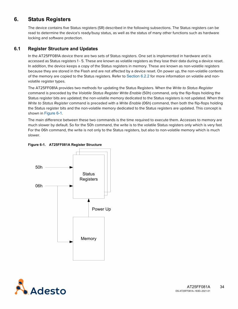
34AT25FF081A DS-AT25FF081A–183D–2021-01
6. Status RegistersThe device contains five Status registers (SR) described in the following subsections. The Status registers can be read to determine the device's ready/busy status, as well as the status of many other functions such as hardware locking and software protection.
6.1 Register Structure and UpdatesIn the AT25FF081A device there are two sets of Status registers. One set is implemented in hardware and is accessed as Status registers 1 - 5. These are known as volatile registers as they lose their data during a device reset. In addition, the device keeps a copy of the Status registers in memory. These are known as non-volatile registers because they are stored in the Flash and are not affected by a device reset. On power up, the non-volatile contents of the memory are copied to the Status registers. Refer to Section 6.2.2 for more information on volatile and non-volatile register types.
The AT25FF081A provides two methods for updating the Status Registers. When the Write to Status Register command is preceded by the Volatile Status Register Write Enable (50h) command, only the flip-flops holding the Status register bits are updated; the non-volatile memory dedicated to the Status registers is not updated. When the Write to Status Register command is preceded with a Write Enable (06h) command, then both the flip-flops holding the Status register bits and the non-volatile memory dedicated to the Status registers are updated. This concept is shown in Figure 6-1.
The main difference between these two commands is the time required to execute them. Accesses to memory are much slower by default. So for the 50h command, the write is to the volatile Status registers only which is very fast. For the 06h command, the write is not only to the Status registers, but also to non-volatile memory which is much slower.
Figure 6-1. AT25FF081A Register Structure
Status Registers
Memory
50h
06h
Power Up

35AT25FF081A DS-AT25FF081A–183D–2021-01
6.2 Register AccessesThis section describes the various ways to access the AT25FF081A Status registers. The AT25FF081A incorporates five Status registers. Each of these registers can be written or read using both the direct and indirect addressing methods as described in Section 6.2.1. In addition, the device supports both volatile and non-volatile registers as described in Section 6.2.2.
6.2.1 Direct and Indirect Addressing
The AT25FF081A device supports both direct and indirect addressing for accessing the Status registers. The indirect addressing method can be used for all five Status registers, and the direct addressing for the first three Status registers. This means that Status registers 4 - 5 can only be accessed using the indirect addressing method.
Historically, Adesto products have supported at most three Status registers. These registers have been accessed using the direct addressing method, where every register has a specific command used to access it and perform read or write operations. An example of these commands is as follows:• 05h: Read Status Register 1• 35h: Read Status Register 2• 15h: Read Status Register 3• 01h: Write Status Register 1• 31h: Write Status Register 2• 11h: Write Status Register 3The above commands have been retained to provide backward compatibility with existing software. In addition to the direct method, the AT25FF081A device also provides an indirect method. In the indirect method, a single command (65h) is used to execute a read operation on all of the Status registers. Another command (71h) is used to execute a write operation on all of the Status registers. Once the command is provided, an 8-bit address field is used to determine which register to access. The encoding of the address field is shown in Table 6-1.
Note that by using the indirect address method, an address width of 8 bits indicates that up to 256 registers can be accessed, allowing for future expansion without requiring additional commands or associated hardware complexity.
6.2.2 Volatile and Non-Volatile Register Accesses
As shown in Figure 6-1, the AT25FF081A device supports both volatile and non-volatile register accesses. Volatile register accesses are to the Status registers implemented in hardware. Non-volatile register accesses are to the
Table 6-1. Indirect Addressing of Status Registers
Command Address Action
65h
01h Read Status Register 1
02h Read Status Register 2
03h Read Status Register 3
04h Read Status Register 4
05h Read Status Register 5
71h
01h Write Status Register 1
02h Write Status Register 2
03h Write Status Register 3
04h Write Status Register 4
05h Write Status Register 5
36AT25FF081A DS-AT25FF081A–183D–2021-01
Status registers stored in memory. During power-up, the contents of the registers in memory are copied to the hardware Status registers.
The preceding 50h or 06h commands determines if the Write Status Register command is to the volatile or non-volatile register set.
6.3 Status Register 1The following table shows the bit assignments for Status register 1.
Table 6-2. Status Register 1 Format
Bit # Acronym Name Type Default Description
7 SRP0 Status Register Protect 0 R/W 0
The SRP0 bit works in conjunction with the SRP1 bit in Status Register 1 and the WP pin to control write protection. Types of protection include software protection, hardware protection, one-time programmable (OTP) protection, and power supply lock-down protection. Refer to Table 6-4 for an encoding of these bits.
6 BPSIZE Block Protect Size R/W 0
The BPSIZE bit controls the size of the blocks protected by the Block Protect Bits (BP2, BP1, BP0 in bits 4:2 of this register). This bit is encoded as follows:0: 64 KB block size 1: 4 KB block sizeThe blocks can also be protected from the bottom up or from the top down as described in the TB bit of this register.
5 TB Top/Bottom R/W 0
The TB bit controls the direction of the blocks to be protected by the Block Protect Bits (BP2, BP1, BP0 in bits 4:2 of this register). This bit is encoded as follows:0: Protect from bottom up 1: Protect from top downThe size of the protected blocks can also be selected as described in the BPSIZE bit of this register.
4:2 BP2:0 Block Protect R/W 000
The 3-bit Block Protect field provides write protection control and status. These bits are set using the Write Status register 1 (01h) command. This field can be programmed to protect all of the memory array, none of the memory array, or a portion of the memory array. When that portion of the memory is selected, it is protected from the Program and Erase commands as described in the Memory Protection table. The default is 3’b000 for this field, indicating that none of the memory array is protected.
37AT25FF081A DS-AT25FF081A–183D–2021-01
1 WEL Write Enable Latch Status R 0
The WEL bit indicates the current status of the internal Write Enable Latch. When the WEL bit is in the logic “0” state, the device does not accept any program, erase, memory protection, or Write Status Register commands. The WEL bit defaults to the logic “0” state after a device power-up or reset.This bit is encoded as follows:0: Device is not write enabled (default). 1: Device is write enabled.If the WEL bit is in the logic “1” state, it will not be reset to a logic “0” if an operation aborts due to an incomplete or unrecognized command being clocked into the device before the CS pin is deasserted. In order for the WEL bit to be reset when an operation aborts prematurely, the entire command for a program, erase, memory protection, or Write Status Register command must have been clocked into the device.When the Write Enable (06h) command is executed, the WEL bit is set. Conversely, when the Volatile Status Register Write Enable (50h) command is executed, the WEL bit is not set.
0 RDY/BSY Ready/Busy Status R 0
The RDY/BSY bit is used to determine whether or not an internal operation, such as a program or erase, is in progress. To poll the RDY/BSY bit to detect the completion of a program or erase cycle, new Status Register data must be continually clocked out of the device until the state of the RDY/BSY bit changes from a logic “1” to a logic “0”.This bit is encoded as follows:0: Device is ready. 1: Device is busy with an internal operation.
Table 6-2. Status Register 1 Format (continued)
Bit # Acronym Name Type Default Description

38AT25FF081A DS-AT25FF081A–183D–2021-01
6.4 Status Register 2The following table shows the bit assignments for Status register 2.
Table 6-3. Status Register 2 Format
Bit # Acronym Name Type Default Description
7 SUSP Suspend Status R 0
The SUSP bit is set by hardware and indicates that the program or erase operation has been suspended. This bit is set after software executes an Erase/Program Suspend (75h) command. Hardware clears this bit when it detects that any of the following events have occurred:
• Erase/Program Resume (7Ah) command• Hardware Reset, JEDEC Hardware Reset• 66h / 99h Reset command
6 CMPRT Complement Protect R/W 0
The CMPRT is used in conjunction with BPSIZE, TB, and BP2:BP0 bits to provide additional memory array protection. This bit is encoded as follows:
0: Current protection mechanism is unchanged 1: Current protection mechanism is reversed
When this bit is set, unprotected areas of memory become protected, and protected areas of memory become unprotected. For example, when CMPRT = 0, a top 64 KB block can be protected while the rest of the array is not; when CMP = 1, the same 64 KB block would become unprotected while the rest of the array becomes read-only.
5:3 SL3:SL1 Security Lock 3:1 R 000
The 3-bit SL3:SL1 field provides a One-Time- Program (OTP) lock status of Security registers 1 - 3. This field is used by software to determine which of these Security registers have been locked. Note that Security register 0 is always locked as the value is programmed by Adesto at the factory.The default state of SL[3:1] is 0, indicating that all registers are unlocked. Each bit corresponds to a Status register as follows:SL3 (bit 5): Security register 3 SL2 (bit 4): Security register 2 SL1 (bit 3): Security register 1Each bit in this field is set by hardware when the most significant byte of the corresponding Security register (the 128th byte) is programmed. For example, when the most significant byte of Security register 1 is set, bit 3 (SL1) of this field is set. Conversely, when the most significant byte of Security register 3 is set, bit 5 (SL3) of this field is set. Each time a bit is set, it indicates that the corresponding 128-Byte Security register has become read-only permanently.
2 R Reserved R 0 Reserved
39AT25FF081A DS-AT25FF081A–183D–2021-01
Table 6-4 shows the operation of the SRP[1:0] volatile Status register bits during normal operation.
1 QE Quad Enable R/W 0
The QE bit enables Quad SPI and XiP operation.This bit is encoded as follows:0: QE mode is disabled 1: QE mode is enabledWhen the QE bit is cleared (logic 0), the WP and HOLD/RESET pins are enabled and perform their respective functions. When the QE bit is set (logic 1), the WP and HOLD/RESET pins function as the IO2 and IO3 pins respectively, and the WP and HOLD/RESET pins functions are disabled.This bit only pertains to the following commands:6Bh: Quad Output Read EBh: XiP Mode Read E7h: XiP Mode Read with Double-word Aligned Address 32h: Quad Output Page Program 77h: Set Burst with Wrap 94h: Quad I/O Read Manufacturer/Device ID
0 SRP1 Status Register Protect 1 R/W 0
The SRP1 bit works in conjunction with the SRP0 bit in Status Register 0 and the WP pin to control write protection. Types of protection include software protection, hardware protection, one-time programmable (OTP) protection, and reset lock-down protection. Refer to Table 6-4 for an encoding of these bits.
Table 6-3. Status Register 2 Format (continued)
Bit # Acronym Name Type Default Description
Table 6-4. Status Register Protection During Normal Operation
SRP1 SRP0 SRLOCK WP Type of Protection Description
0 0 x x
Software Protected(protection is controlled by the CMPRT, BPSIZE, TB,
BP[2:0], or WPS bits)
When both the SRP0 and SRP1 bits are 0, the Status registers can be written by executing a Write Status Register command (01h, 31h, 11h, 71h) and setting the WEL bit of this register. Note that the WP pin has no meaning during this type of operation.
0 1 x 0Hardware Protected
(protection is controlled by the WP pin)
When the SRP[1:0] bits are 0, 1 respectively, and the WP pin is low, the registers are hardware protected and cannot be written to.
0 1 x 1
Hardware Unprotected(protection is controlled by the CMPRT, BPSIZE, TB,
BP[2:0], or WPS bits)
When the SRP[1:0] bits are 0, 1 respectively, and the WP pin is high, the registers are not hardware protected and can be written to by executing a Write Status Register command (01h, 31h, 11h, 71h) and setting the WEL bit of this register.
1 0 x x Reset Lockdown
When the SRP[1:0] bits are 1, 0 respectively, the Status registers are write protected and cannot be written until the device is reset (caused by a power-cycle, hardware reset, or software reset). After reset, hardware changes the state of the SRP[1:0] bits as shown in Table 6-5.
1 1 0 x Reset Lockdown
When the SRP[1:0] bits are 1,1 respectively, and the SRLOCK bit is 0, the Status registers are write protected and cannot be written until the device is reset (caused by a power-cycle, hardware reset or software reset). After reset, hardware changes the state of SRP[1:0] bits as shown in Table 6-5.

40AT25FF081A DS-AT25FF081A–183D–2021-01
Table 6-5 shows the behavior of the SRP1 and SPR0 bits after a reset condition.
6.5 Status Register 3The following table shows the bit assignments for Status register 3.
1 1 1 x OTPWhen the SRP[1:0] bits are 1,1 respectively, and the SRLOCK bit is 1, the Status registers are permanently write protected.
Table 6-4. Status Register Protection During Normal Operation (continued)
SRP1 SRP0 SRLOCK WP Type of Protection Description
Table 6-5. Status Register Protection During Reset
Non-Volatile Memory Bits Type of Protection Description
Volatile Register Bits
SRP1 SRP0 SRLOCK SRP1 SRP0
0 0 x Software Protected
The reset operation maintains the volatile SRP1 and SRP0 at 0,0. 0 0
0 1 x Hardware Protected
The reset operation maintains the volatile SRP1 and SRP0 at 0,1. 0 1
1 0 x Reset Lockdown
The reset operation changes the volatile SRP1 and SRP0 bits to 0,0. 0 0
1 1 0 Reset Lockdown
The reset operation changes the volatile SRP1 and SRP0 bits to 0,1. 0 1
1 1 1One-Time Program (OTP)
The reset operation maintains the volatile SRP1 and SRP0 at 1,1. This makes the Status registers permanently write protected.
1 1
Table 6-6. Status Register 3 Format
Bit # Acronym Name Type Default Description
7 HOLD/RESET
HOLD or RESET Function R/W 0
Adesto provides a variety of packages for the AT25FF081A as shown in Section 2. Each of these packages provides a dedicated HOLD/RESET pin that can be configured as a RESET pin, or as a HOLD pin, depending on the programming of this bit. This bit is encoded as follows:0: HOLD function is enabled 1: RESET function is enabledNote that this pin can only be configured as HOLD or RESET when the QE bit (see bit 1 of Status register 2) is cleared (logic 0). If the QE bit is set, the pin functions as a dedicated data pin and the HOLD/RESET functionality is disabled.
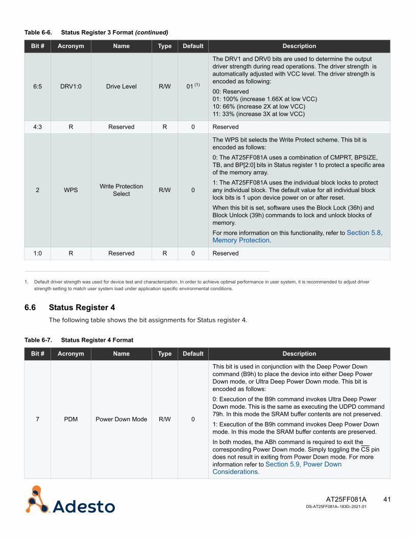
41AT25FF081A DS-AT25FF081A–183D–2021-01
6.6 Status Register 4The following table shows the bit assignments for Status register 4.
6:5 DRV1:0 Drive Level R/W 01 (1)
The DRV1 and DRV0 bits are used to determine the output driver strength during read operations. The driver strength is automatically adjusted with VCC level. The driver strength is encoded as following:00: Reserved 01: 100% (increase 1.66X at low VCC) 10: 66% (increase 2X at low VCC) 11: 33% (increase 3X at low VCC)
4:3 R Reserved R 0 Reserved
2 WPS Write Protection Select R/W 0
The WPS bit selects the Write Protect scheme. This bit is encoded as follows:0: The AT25FF081A uses a combination of CMPRT, BPSIZE, TB, and BP[2:0] bits in Status register 1 to protect a specific area of the memory array.1: The AT25FF081A uses the individual block locks to protect any individual block. The default value for all individual block lock bits is 1 upon device power on or after reset. When this bit is set, software uses the Block Lock (36h) and Block Unlock (39h) commands to lock and unlock blocks of memory.For more information on this functionality, refer to Section 5.8, Memory Protection.
1:0 R Reserved R 0 Reserved
1. Default driver strength was used for device test and characterization. In order to achieve optimal performance in user system, it is recommended to adjust driver strength setting to match user system load under application specific environmental conditions.
Table 6-6. Status Register 3 Format (continued)
Bit # Acronym Name Type Default Description
Table 6-7. Status Register 4 Format
Bit # Acronym Name Type Default Description
7 PDM Power Down Mode R/W 0
This bit is used in conjunction with the Deep Power Down command (B9h) to place the device into either Deep Power Down mode, or Ultra Deep Power Down mode. This bit is encoded as follows:0: Execution of the B9h command invokes Ultra Deep Power Down mode. This is the same as executing the UDPD command 79h. In this mode the SRAM buffer contents are not preserved.1: Execution of the B9h command invokes Deep Power Down mode. In this mode the SRAM buffer contents are preserved.In both modes, the ABh command is required to exit the corresponding Power Down mode. Simply toggling the CS pin does not result in exiting from Power Down mode. For more information refer to Section 5.9, Power Down Considerations.

42AT25FF081A DS-AT25FF081A–183D–2021-01
6 SPMSequential
Program Mode Status
R 0
The SPM bit indicates whether the device is in the Byte/Page Program mode or the Sequential Program Mode. The default state after power-up or device reset is the Byte/Page Program mode. This bit is encoded as follows:0: Byte/Page Programming Mode (default) 1: Sequential Programming Mode enteredIf this bit is 1, the address is only required for the first transfer of the sequential operation. Therefore, on the first transfer, command, address, and data are required. If there are subsequent operations, the address is not required. Software need only supply the command and data (on a write).
5 PE Program Error R 0 This bit is set by hardware whenever an error occurs during a program operation.
4 EE Erase Error R 0 This bit is set by hardware whenever an error occurs during an erase operation.
3 XiP XiP Mode Select R/W 0
This bit determines whether a command is required each time a read operation is executed using the E7h or EBh (Quad Read) commands. This bit is encoded as follows:0: XiP mode (continuous read mode) is disabled1: XiP mode (continuous read mode) is enabledIf this bit is set and either the E7h or EBh commands are executed, the command is only required for the first access (1-4-4). In this case, the command is transferred on the SI pin, and the address and data are transferred on the SI (I/O0), SO (I/O1), WP (I/O2), and HOLD (I/O3) pins. Subsequent accesses require only address and data (0-4-4). Note that if either this bit or the QE bit (see bit 1 of Status register 2) is 0, the device can never be placed into 0-4-4 mode, and a command is required for each access.
2:0 BWS[2:0] Burst Wrap Settings R 001
This 3-bit field maps to the W6:W4 bits of the Set Burst Wrap command (77h) to determine the burst wrap status and the wrap length. Refer to Section 7.13 for more information on the Set Burst Wrap command and an encoding of this field.
Table 6-7. Status Register 4 Format (continued)
Bit # Acronym Name Type Default Description
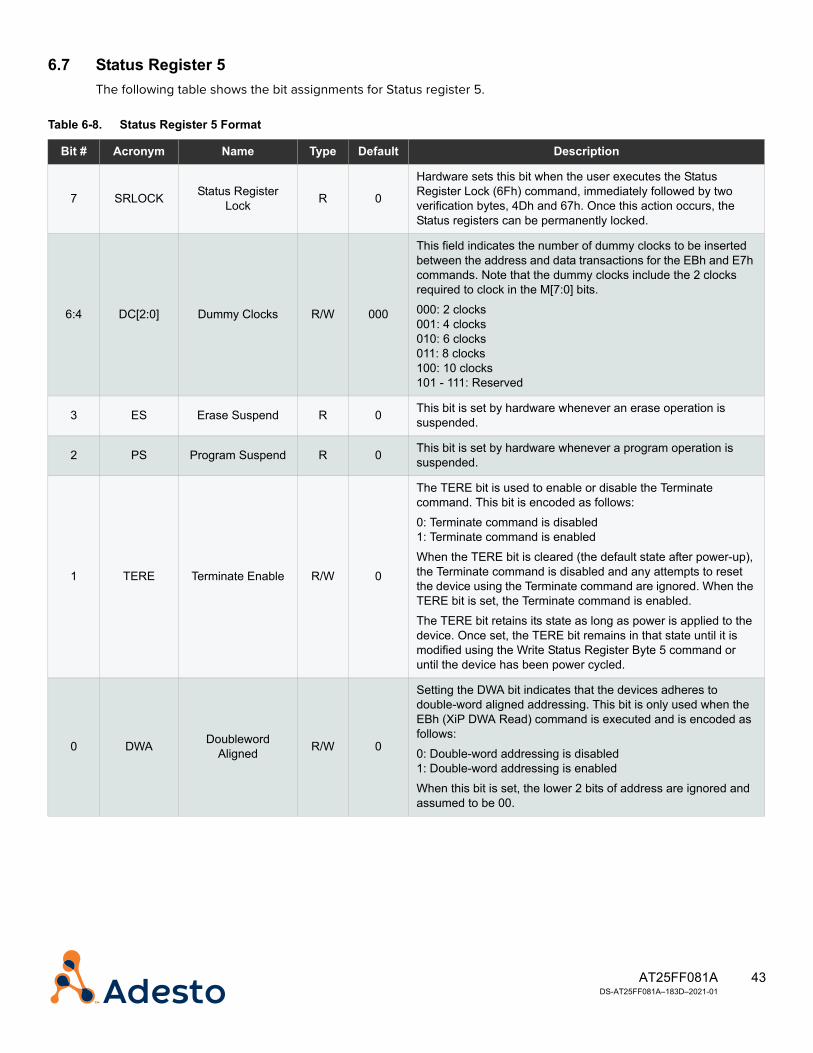
43AT25FF081A DS-AT25FF081A–183D–2021-01
6.7 Status Register 5 The following table shows the bit assignments for Status register 5.
Table 6-8. Status Register 5 Format
Bit # Acronym Name Type Default Description
7 SRLOCK Status Register Lock R 0
Hardware sets this bit when the user executes the Status Register Lock (6Fh) command, immediately followed by two verification bytes, 4Dh and 67h. Once this action occurs, the Status registers can be permanently locked.
6:4 DC[2:0] Dummy Clocks R/W 000
This field indicates the number of dummy clocks to be inserted between the address and data transactions for the EBh and E7h commands. Note that the dummy clocks include the 2 clocks required to clock in the M[7:0] bits.000: 2 clocks 001: 4 clocks 010: 6 clocks 011: 8 clocks 100: 10 clocks 101 - 111: Reserved
3 ES Erase Suspend R 0 This bit is set by hardware whenever an erase operation is suspended.
2 PS Program Suspend R 0 This bit is set by hardware whenever a program operation is suspended.
1 TERE Terminate Enable R/W 0
The TERE bit is used to enable or disable the Terminate command. This bit is encoded as follows:0: Terminate command is disabled 1: Terminate command is enabledWhen the TERE bit is cleared (the default state after power-up), the Terminate command is disabled and any attempts to reset the device using the Terminate command are ignored. When the TERE bit is set, the Terminate command is enabled.The TERE bit retains its state as long as power is applied to the device. Once set, the TERE bit remains in that state until it is modified using the Write Status Register Byte 5 command or until the device has been power cycled.
0 DWA Doubleword Aligned R/W 0
Setting the DWA bit indicates that the devices adheres to double-word aligned addressing. This bit is only used when the EBh (XiP DWA Read) command is executed and is encoded as follows:0: Double-word addressing is disabled 1: Double-word addressing is enabledWhen this bit is set, the lower 2 bits of address are ignored and assumed to be 00.
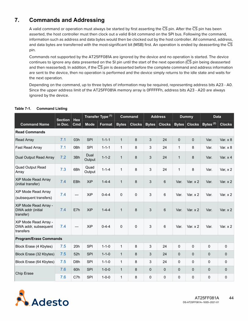
44AT25FF081A DS-AT25FF081A–183D–2021-01
7. Commands and AddressingA valid command or operation must always be started by first asserting the CS pin. After the CS pin has been asserted, the host controller must then clock out a valid 8-bit command on the SPI bus. Following the command, information such as address and data bytes would then be clocked out by the host controller. All command, address, and data bytes are transferred with the most-significant bit (MSB) first. An operation is ended by deasserting the CS pin.
Commands not supported by the AT25FF081A are ignored by the device and no operation is started. The device continues to ignore any data presented on the SI pin until the start of the next operation (CS pin being deasserted and then reasserted). In addition, if the CS pin is deasserted before the complete command and address information are sent to the device, then no operation is performed and the device simply returns to the idle state and waits for the next operation.
Depending on the command, up to three bytes of information may be required, representing address bits A23 - A0. Since the upper address limit of the AT25FF081A memory array is 0FFFFFh, address bits A23 - A20 are always ignored by the device.
Table 7-1. Command Listing
Command NameSection in Doc.
Hex Cmd
Transfer Type (1) Command Address Dummy Data
Mode Format Bytes Clocks Bytes Clocks Bytes Clocks Bytes (2) Clocks
Read Commands
Read Array 7.1 03h SPI 1-1-1 1 8 3 24 0 0 Var. Var. x 8
Fast Read Array 7.1 0Bh SPI 1-1-1 1 8 3 24 1 8 Var. Var. x 8
Dual Output Read Array 7.2 3Bh Dual Output 1-1-2 1 8 3 24 1 8 Var. Var. x 4
Quad Output Read Array 7.3 6Bh Quad
Output 1-1-4 1 8 3 24 1 8 Var. Var, x 2
XiP Mode Read Array (initial transfer) 7.4 EBh XiP 1-4-4 1 8 3 6 Var. Var. x 2 Var. Var. x 2
XiP Mode Read Array(subsequent transfers)
7.4 --- XiP 0-4-4 0 0 3 6 Var. Var. x 2 Var. Var. x 2
XiP Mode Read Array - DWA addr (initial transfer)
7.4 E7h XiP 1-4-4 1 8 3 6 Var. Var. x 2 Var. Var. x 2
XiP Mode Read Array - DWA addr, subsequent transfers
7.4 --- XiP 0-4-4 0 0 3 6 Var. Var. x 2 Var. Var. x 2
Program/Erase Commands
Block Erase (4 Kbytes) 7.5 20h SPI 1-1-0 1 8 3 24 0 0 0 0
Block Erase (32 Kbytes) 7.5 52h SPI 1-1-0 1 8 3 24 0 0 0 0
Block Erase (64 Kbytes) 7.5 D8h SPI 1-1-0 1 8 3 24 0 0 0 0
Chip Erase7.6 60h SPI 1-0-0 1 8 0 0 0 0 0 0
7.6 C7h SPI 1-0-0 1 8 0 0 0 0 0 0
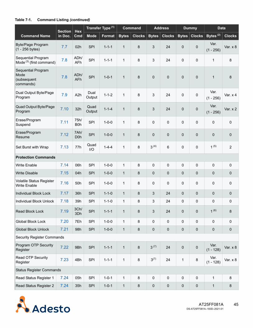
45AT25FF081A DS-AT25FF081A–183D–2021-01
Byte/Page Program (1 - 256 bytes) 7.7 02h SPI 1-1-1 1 8 3 24 0 0
Var.(1 - 256)
Var. x 8
Sequential Program Mode (3) (first command) 7.8 ADh/
AFh SPI 1-1-1 1 8 3 24 0 0 1 8
Sequential Program Mode (subsequent commands)
7.8 ADh/AFh SPI 1-0-1 1 8 0 0 0 0 1 8
Dual Output Byte/Page Program 7.9 A2h Dual
Output 1-1-2 1 8 3 24 0 0Var.
(1 - 256)Var. x 4
Quad Output Byte/Page Program 7.10 32h Quad
Output 1-1-4 1 8 3 24 0 0Var.
(1 - 256)Var. x 2
Erase/Program Suspend 7.11 75h/
B0h SPI 1-0-0 1 8 0 0 0 0 0 0
Erase/Program Resume 7.12 7Ah/
D0h SPI 1-0-0 1 8 0 0 0 0 0 0
Set Burst with Wrap 7.13 77h Quad I/O 1-4-4 1 8 3 (4) 6 0 0 1 (5) 2
Protection Commands
Write Enable 7.14 06h SPI 1-0-0 1 8 0 0 0 0 0 0
Write Disable 7.15 04h SPI 1-0-0 1 8 0 0 0 0 0 0
Volatile Status Register Write Enable 7.16 50h SPI 1-0-0 1 8 0 0 0 0 0 0
Individual Block Lock 7.17 36h SPI 1-1-0 1 8 3 24 0 0 0 0
Individual Block Unlock 7.18 39h SPI 1-1-0 1 8 3 24 0 0 0 0
Read Block Lock 7.19 3Ch/3Dh SPI 1-1-1 1 8 3 24 0 0 1 (6) 8
Global Block Lock 7.20 7Eh SPI 1-0-0 1 8 0 0 0 0 0 0
Global Block Unlock 7.21 98h SPI 1-0-0 1 8 0 0 0 0 0 0
Security Register Commands
Program OTP Security Register 7.22 9Bh SPI 1-1-1 1 8 3 (7) 24 0 0 Var.
(1 - 128) Var. x 8
Read OTP Security Register 7.23 4Bh SPI 1-1-1 1 8 3(7) 24 1 8 Var.
(1 - 128) Var. x 8
Status Register Commands
Read Status Register 1 7.24 05h SPI 1-0-1 1 8 0 0 0 0 1 8
Read Status Register 2 7.24 35h SPI 1-0-1 1 8 0 0 0 0 1 8
Table 7-1. Command Listing (continued)
Command NameSection in Doc.
Hex Cmd
Transfer Type (1) Command Address Dummy Data
Mode Format Bytes Clocks Bytes Clocks Bytes Clocks Bytes (2) Clocks
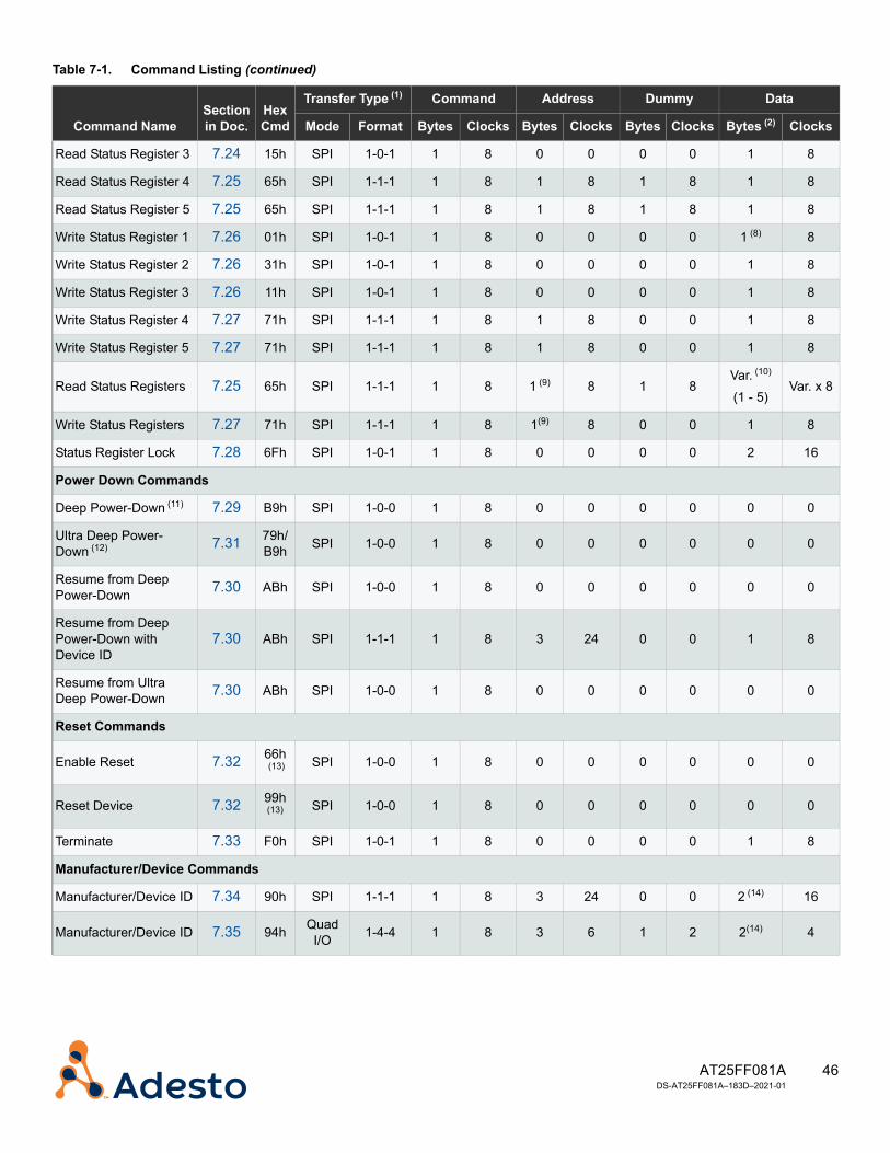
46AT25FF081A DS-AT25FF081A–183D–2021-01
Read Status Register 3 7.24 15h SPI 1-0-1 1 8 0 0 0 0 1 8
Read Status Register 4 7.25 65h SPI 1-1-1 1 8 1 8 1 8 1 8
Read Status Register 5 7.25 65h SPI 1-1-1 1 8 1 8 1 8 1 8
Write Status Register 1 7.26 01h SPI 1-0-1 1 8 0 0 0 0 1 (8) 8
Write Status Register 2 7.26 31h SPI 1-0-1 1 8 0 0 0 0 1 8
Write Status Register 3 7.26 11h SPI 1-0-1 1 8 0 0 0 0 1 8
Write Status Register 4 7.27 71h SPI 1-1-1 1 8 1 8 0 0 1 8
Write Status Register 5 7.27 71h SPI 1-1-1 1 8 1 8 0 0 1 8
Read Status Registers 7.25 65h SPI 1-1-1 1 8 1 (9) 8 1 8Var. (10)
(1 - 5)Var. x 8
Write Status Registers 7.27 71h SPI 1-1-1 1 8 1(9) 8 0 0 1 8
Status Register Lock 7.28 6Fh SPI 1-0-1 1 8 0 0 0 0 2 16
Power Down Commands
Deep Power-Down (11) 7.29 B9h SPI 1-0-0 1 8 0 0 0 0 0 0
Ultra Deep Power-Down (12) 7.31 79h/
B9h SPI 1-0-0 1 8 0 0 0 0 0 0
Resume from Deep Power-Down 7.30 ABh SPI 1-0-0 1 8 0 0 0 0 0 0
Resume from Deep Power-Down with Device ID
7.30 ABh SPI 1-1-1 1 8 3 24 0 0 1 8
Resume from Ultra Deep Power-Down 7.30 ABh SPI 1-0-0 1 8 0 0 0 0 0 0
Reset Commands
Enable Reset 7.32 66h (13) SPI 1-0-0 1 8 0 0 0 0 0 0
Reset Device 7.32 99h (13) SPI 1-0-0 1 8 0 0 0 0 0 0
Terminate 7.33 F0h SPI 1-0-1 1 8 0 0 0 0 1 8
Manufacturer/Device Commands
Manufacturer/Device ID 7.34 90h SPI 1-1-1 1 8 3 24 0 0 2 (14) 16
Manufacturer/Device ID 7.35 94h Quad I/O 1-4-4 1 8 3 6 1 2 2(14) 4
Table 7-1. Command Listing (continued)
Command NameSection in Doc.
Hex Cmd
Transfer Type (1) Command Address Dummy Data
Mode Format Bytes Clocks Bytes Clocks Bytes Clocks Bytes (2) Clocks
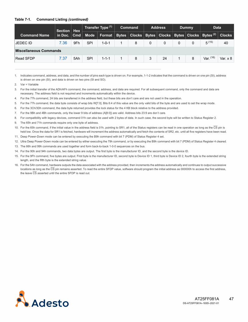
47AT25FF081A DS-AT25FF081A–183D–2021-01
JEDEC ID 7.36 9Fh SPI 1-0-1 1 8 0 0 0 0 5 (15) 40
Miscellaneous Commands
Read SFDP 7.37 5Ah SPI 1-1-1 1 8 3 24 1 8 Var. (16) Var. x 8
1. Indicates command, address, and data, and the number of pins each type is driven on. For example, 1-1-2 indicates that the command is driven on one pin (SI), address is driven on one pin (SI), and data is driven on two pins (SI and SO).
2. Var = Variable
3. For the initial transfer of the ADh/AFh command, the command, address, and data are required. For all subsequent command, only the command and data are necessary. The address field is not required and increments automatically within the device.
4. For the 77h command, 24 bits are transferred in the address field, but these bits are don’t care and are not used in the operation.
5. For the 77h command, the data byte consists of wrap bits W[7:0]. Bits 6:4 of this value are the only valid bits of the byte and are used to set the wrap mode.
6. For the 3Ch/3Dh command, the data byte returned provides the lock status for the 4 KB block relative to the address provided.
7. For the 9Bh and 4Bh commands, only the lower 9 bits of address (A[8:0]) are valid. Address bits 23:9 are don’t care.
8. For compatibility with legacy devices, command 01h can also be used with 2 bytes of data. In such case, the second byte will be written to Status Register 2.
9. The 65h and 71h commands require only one byte of address.
10. For the 65h command, if the initial value in the address field is 01h, pointing to SR1, all of the Status registers can be read in one operation as long as the CS pin is held low. Once the data for SR1 is fetched, hardware will increment the address automatically and fetch the contents of SR2, etc. until all five registers have been read.
11. Deep Power-Down mode can be entered by executing the B9h command with bit 7 (PDM) of Status Register 4 set.
12. Ultra Deep Power-Down mode can be entered by either executing the 79h command, or by executing the B9h command with bit 7 (PDM) of Status Register 4 cleared.
13. The 66h and 99h commands are used together and form back-to-back 1-0-0 sequences on the bus.
14. For the 90h and 94h commands, two data bytes are output. The first byte is the manufacturer ID, and the second byte is the device ID.
15. For the 9Fh command, five bytes are output. First byte is the manufacturer ID, second byte is Device ID 1, third byte is Device ID 2, fourth byte is the extended string length, and the fifth byte is the extended string value.
16. For the 5Ah command, hardware outputs the data associated with the address provided, then increments the address automatically and continues to output successive locations as long as the CS pin remains asserted. To read the entire SFDP value, software should program the initial address as 000000h to access the first address, the leave CS asserted until the entire SFDP is read out.
Table 7-1. Command Listing (continued)
Command NameSection in Doc.
Hex Cmd
Transfer Type (1) Command Address Dummy Data
Mode Format Bytes Clocks Bytes Clocks Bytes Clocks Bytes (2) Clocks
48AT25FF081A DS-AT25FF081A–183D–2021-01
7.1 Read Array (03h, 0Bh)The Read Array command can be used to sequentially read a continuous stream of data from the device by simply providing the clock signal once the initial starting address is specified. The device incorporates an internal address counter that automatically increments every time one byte of data is output by the device.
Two commands (0Bh and 03h) can be used to read the memory array. The use of each command depends on the maximum clock frequency that is used to read data from the device. The 0Bh command can be used at any clock frequency up to the maximum specified by fSCK, and the 03h command can be used for lower frequency read operations up to the maximum specified by fRDLF.
7.1.1 Command Prerequisites
None.
7.1.2 Transfer Format
The 03h/0Bh command follows the 1-1-1 transfer format described in Section 5.2, where the command and address are transferred on the SI pin, and data is transferred on the SO pin. Refer to Figure 5-5 for timing diagram of a 1-1-1 transfer showing the toggling of external bus signals for a read operation without dummy bytes. Figure 5-6 shows a read operation with dummy bytes.
7.1.3 Transfer Sequence
To perform the Read Array command, the CS pin is asserted and the information transferred as follows: • Assert the CS pin.• The appropriate command (0Bh or 03h) is clocked into the device. Eight clocks are required to transfer the com-
mand. The most significant bit of the command is transferred first.• Three address bytes are clocked in to specify the starting address location of the first byte to read within the
memory array. A total of 24 clocks are required to transfer the address. The most significant bit of the address (A[23]) is transferred first.
• Following the three address bytes, an additional dummy byte must be clocked into the device if the 0Bh com-mand is used.
• Data is output on the SO pin. Each byte transfer requires eight clock cycles. The number of bytes transferred is determined by software. The transfer can be anywhere from a single byte to the entire memory array. The most significant bit of each data byte is transferred first.
• Deasserting the CS pin terminates the read operation and puts the SO pin into high-impedance state. The CS pin can be deasserted at any time and does not require a full byte of data be read.
Refer to Table 7-1 for more information on the transfer sequence for this command.
When the last byte (0FFFFFh) of the memory array has been read, the device loops back and continues reading at the beginning of the array (000000h). No delays are incurred when wrapping around from the end of the array to the beginning of the array.
7.1.4 Programming Restrictions
None
49AT25FF081A DS-AT25FF081A–183D–2021-01
7.2 Dual Output Read Array (3Bh)The Dual Output Read Array command is similar to the standard Read Array (03h/0Bh) command and can be used to sequentially read a continuous stream of data from the device by simply providing the clock signal once the initial starting address has been specified. Unlike the standard Read Array command, however, the Dual Output Read Array command allows two bits of data to be clocked out of the device on every clock cycle, rather than just one.
7.2.1 Command Prerequisites
None.
7.2.2 Transfer Format
The 3Bh command follows the 1-1-2 transfer format described in Section 5.3, where the command and address are transferred on the SI pin, and output data is transferred on the SI and SO pin. To facilitate this transfer, hardware switches the SI pin to an output as soon as the command has been decoded and the address transferred. Refer to Figure 5-8 for a timing diagram of this command.
7.2.3 Transfer Sequence
To perform the Dual Output Read Array operation, the CS pin is asserted and the information transferred as follows:• The 3Bh command is clocked into the device. Eight clocks are required to transfer the command. The most sig-
nificant bit of the command is transferred first.• Three address bytes are clocked in to specify the starting address location of the first byte to read within the
memory array. A total of 24 clocks are required to transfer the address. The most significant bit of the address (A[23]) is transferred first.
• Following the three address bytes, an additional dummy byte must be clocked into the device. This requires eight clock cycles to complete.
• Data is output on the SI and SO pins. As a result, each byte transfer requires four clock cycles, half that of the 03h/0Bh commands. The data is always output with the most significant bit of the byte transferred first. The number of bytes transferred is determined by software. The transfer can be anywhere from a single byte to the entire memory array. The data is driven onto the bus as follows:- 1st data clock: bit 7 is output on the SO pin- 1st data clock: bit 6 is output on the SI pin- 2nd data clock: bit 5 is output on the SO pin- 2nd data clock: bit 4 is output on the SI pin- 3rd data clock: bit 3 is output on the SO pin- 3rd data clock: bit 2 is output on the SI pin- 4th data clock: bit 1 is output on the SO pin- 4th data clock: bit 0 is output on the SI pin- Subsequent bytes are output with each additional 4 clocks. The sequence above continues with each byte of
data being output after every four clock cycles.• Deasserting the CS pin terminates the read operation and puts the SO and SI pins into a high-impedance state.
The CS pin can be deasserted at any time and does not require that a full byte of data be read.When the last byte (0FFFFFh) of the memory array has been read, the device continues reading from the beginning of the array (000000h). No delays are incurred when wrapping around from the end of the array to the beginning of the array.
7.2.4 Programming Restrictions
None

50AT25FF081A DS-AT25FF081A–183D–2021-01
7.3 Quad Output Read Array (6Bh)The Quad Output Read Array command is similar to the Dual Output Read Array command, except that the Quad Output Read Array command allows four bits of data to be clocked out of the device on every clock cycle, rather than just one or two. Note that the Quad Enable bit (QE) in Status Register 2 (SR2) must be set to enable this command. The Quad Output Read Array command can be used at any clock frequency, up to the maximum specified by fSCK.
7.3.1 Command Prerequisites
None.
7.3.2 Transfer Format
The 6Bh command follows the 1-1-4 transfer format described in Section 5.5, where the command and address are transferred on the SI pin, and data is transferred on the HOLD, WP, SO, and SI pins. Refer to Figure 5-12 for a timing diagram of this transaction.
7.3.3 Transfer Sequence
To perform the Quad Output Read Array operation, the CS pin is asserted and the information transferred as follows:• The 6Bh command is clocked into the device. Eight clocks are required to transfer the command. The most sig-
nificant bit of the command is transferred first.• Three address bytes are clocked in to specify the starting address location of the first byte to read within the
memory array. A total of 24 clocks are required to transfer the address. The most significant bit of the address (A[23]) is transferred first.
• Following the three address bytes, an additional dummy byte must be clocked into the device. This requires eight clock cycles to complete.
• Following transfer of the dummy byte, hardware switches the HOLD, WP, and SI pins to outputs.• Data is output on the HOLD, WP, SO, and SI pins. As a result, each byte transfer requires two clock cycles, one-
fourth that of the 03h/0Bh commands. The data is always output with the most significant bit of the byte trans-ferred first. The number of bytes transferred is determined by software. The transfer can be anywhere from a single byte to the entire memory array. Each data byte is shifted out of the device as follows: - First data clock: bit 7 is output on the HOLD pin- First data clock: bit 6 is output on the WP pin- First data clock: bit 5 is output on the SO pin- First data clock: bit 4 is output on the SI pin- Second data clock: bit 3 is output on the HOLD pin- Second data clock: bit 2 is output on the WP pin- Second data clock: bit 1 is output on the SO pin- Second data clock: bit 0 is output on the SI pin
• Deasserting the CS pin terminates the read operation and puts the HOLD, WP, SO, SI pins into a high-imped-ance state. The CS pin can be deasserted at any time and does not require that a full byte of data be read.
When the last byte (0FFFFFh) of the memory array has been read, the device continues reading from the beginning of the array (000000h). No delays are incurred when wrapping around from the end of the array to the beginning of the array.
7.3.4 Programming Restrictions
None

51AT25FF081A DS-AT25FF081A–183D–2021-01
7.4 XiP Read (EBh), XiP Read with Double-word Aligned Address (E7h)The XiP Read command (EBh) is similar to the Quad Output Read Array command, except that four bits of address are clocked into the device on every clock cycle, rather than just one. The E7h command is similar to the EBh command but works only on double-word aligned (DWA) addresses. As such, the E7h command ignores address bits A[1:0] and internally assumes that these two bits are always 2'b00. This allows us to run the E7h command at faster clock speeds or fewer dummy clock cycles compared to the EBh command.
The EBh command can operate in either DWA mode or non-DWA mode depending on the state of the DWA bit in Status Register 5. Refer to Section 6.7, Status Register 5 for more information.
7.4.1 Command Prerequisites
None.
7.4.2 Transfer Format
The initial EBh/E7h command follows the 1-4-4 transfer format described in Section 5.6, where the command is transferred on the SI pin, and the address and data are transferred on the SI (IO0), SO (IO1), WP (IO2), and HOLD (IO3) pins. Refer to Figure 5-13 for a timing diagram of this command.
Subsequent EBh/E7h commands follow the 0-4-4 transfer format described in Section 5.6, where the address and data are transferred on the SI (IO0), SO (IO1), WP (IO2), and HOLD (IO3) pins. No command transfer is required. Refer to Figure 5-14 for a timing diagram of this command.
7.4.3 Mode Bits
The EBh and E7h commands follow the 1-4-4 and 0-4-4 transfer formats as described above. During the initial transfer, an 8-bit mode field is transferred immediately following the last address byte and is decoded by hardware to determine if the device should be placed into XiP continuous read mode. If so, then subsequent transfers do not require the command field, resulting in a 0-4-4 transfer type. This mode increases performance by saving 8 clocks cycles per transfer. For more information on this mode, refer to Section 5.6, XiP Mode Operation.
7.4.4 Transfer Sequence — Initial Transfer
To perform the initial XiP Mode Read operation, the CS pin is asserted and the information transferred as follows:• The EBh/E7h command is clocked into the device. Eight clocks are required to transfer the command. The most
significant bit of the command is transferred first. This field is transferred on the SI pin.• Three address bytes are clocked in to specify the starting address location of the first byte to read within the
memory array. A total of 6 clocks are required to transfer the address. The most significant bit of the address (A[23]) is transferred first. Each address byte is shifted out of the device as follows: - First clock: address bit 23 is input on the HOLD pin- First clock: address bit 22 is input on the WP pin- First clock: address bit 21 is input on the SO pin- First clock: address bit 20 is input on the SI pin- Second clock: address bit 19 is input on the HOLD pin- Second clock: address bit 18 is input on the WP pin- Second clock: address bit 17 is input on the SO pin- Second clock: address bit 16 is input on the SI pin- Third and fourth clocks: A15:A8 are shifted in same as above- Fifth and sixth clocks: A7:A0 are shifted in same as above
• Following the three address bytes, a programmable number of dummy bytes must be clocked into the device. Refer to the Section 7.4.6 below for more information. Note that the Mode bits are treated as part of the dummy bytes and must be clocked in to the device.
52AT25FF081A DS-AT25FF081A–183D–2021-01
• Following transfer of the dummy bytes, hardware switches the SI (IO0), SO (IO1), WP (IO2), and HOLD (IO3) pins to outputs.
• Data is output on the HOLD, WP, SO, and SI pins. As a result, each byte transfer requires two clock cycles. The data is always output with the most significant bit of the byte transferred first. Each data byte is shifted out of the device as follows: - First clock: bit 7 is output on the HOLD pin- First clock: bit 6 is output on the WP pin- First clock: bit 5 is output on the SO pin- First clock: bit 4 is output on the SI pin- Second clock: bit 3 is output on the HOLD pin- Second clock: bit 2 is output on the WP pin- Second clock: bit 1 is output on the SO pin- Second clock: bit 0 is output on the SI pin
• Deasserting the CS pin terminates the read operation and puts the SI (IO0), SO (IO1), WP (IO2), and HOLD (IO3) pins into a high-impedance state. The CS pin can be deasserted at any time and does not require that a full byte of data be read.
• When the last byte (0FFFFFh) of the memory array has been read, the device continues reading from the begin-ning of the array (000000h). No delays are incurred when wrapping around from the end of the array to the beginning of the array.
7.4.5 Transfer Sequence — Subsequent Transfers
To perform subsequent XiP Mode Read operations, the CS pin is asserted and the information transferred as follows:• Three address bytes are clocked in to specify the starting address location of the first byte to read within the
memory array. A total of 6 clocks are required to transfer the address. The most significant bit of the address (A[23]) is transferred first. The address is transferred on the bus in the same manner described in Section 7.4.4 above.
• Following the three address bytes, a programmable number of dummy bytes must be clocked into the device. Refer to Section 7.4.6 below for more information. Note that the Mode bits are treated as part of the dummy bytes and must be clocked in to the device.
• Data is output on the HOLD, WP, SO, and SI pins. As a result, each byte transfer requires two clock cycles. The data is always output with the most significant bit of the byte transferred first. Data is shifted out onto the bus in the same manner described in Section 7.4.4 above.
• Deasserting the CS pin terminates the read operation and puts the SI (IO0), SO (IO1), WP (IO2), and HOLD (IO3) pins into a high-impedance state. The CS pin can be deasserted at any time and does not require that a full byte of data be read.
When the last byte (0FFFFFh) of the memory array has been read, the device continues reading from the beginning of the array (000000h). No delays are incurred when wrapping around from the end of the array to the beginning of the array.
7.4.6 Programmable Number of Dummy Clocks
The number of dummy clocks required differs depending on the frequency, the type of command being performed, and the state of bit 0 (DWA) of Status register 5. This relationship is shown in the table below. The number of Dummy clocks is set using bits 6:4 (DC[2:0]) of Status register 5. Refer to Section 6.7, Status Register 5 for more information. Note that the number of dummy clocks includes the 2 SCK clock periods required to clock in the M[7:0] mode bits.
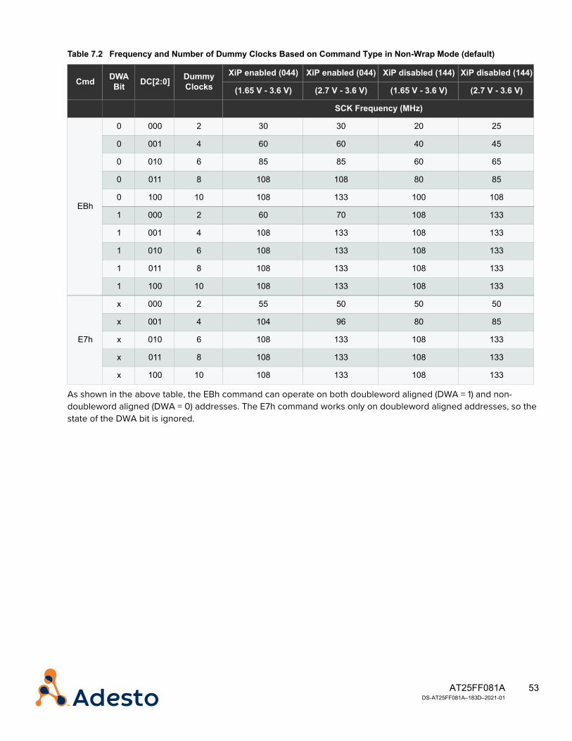
53AT25FF081A DS-AT25FF081A–183D–2021-01
As shown in the above table, the EBh command can operate on both doubleword aligned (DWA = 1) and non-doubleword aligned (DWA = 0) addresses. The E7h command works only on doubleword aligned addresses, so the state of the DWA bit is ignored.
Table 7.2 Frequency and Number of Dummy Clocks Based on Command Type in Non-Wrap Mode (default)
Cmd DWA Bit DC[2:0] Dummy
ClocksXiP enabled (044) XiP enabled (044) XiP disabled (144) XiP disabled (144)
(1.65 V - 3.6 V) (2.7 V - 3.6 V) (1.65 V - 3.6 V) (2.7 V - 3.6 V)
SCK Frequency (MHz)
EBh
0 000 2 30 30 20 25
0 001 4 60 60 40 45
0 010 6 85 85 60 65
0 011 8 108 108 80 85
0 100 10 108 133 100 108
1 000 2 60 70 108 133
1 001 4 108 133 108 133
1 010 6 108 133 108 133
1 011 8 108 133 108 133
1 100 10 108 133 108 133
E7h
x 000 2 55 50 50 50
x 001 4 104 96 80 85
x 010 6 108 133 108 133
x 011 8 108 133 108 133
x 100 10 108 133 108 133
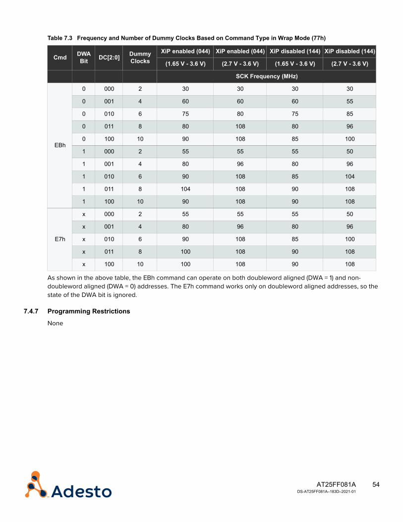
54AT25FF081A DS-AT25FF081A–183D–2021-01
As shown in the above table, the EBh command can operate on both doubleword aligned (DWA = 1) and non-doubleword aligned (DWA = 0) addresses. The E7h command works only on doubleword aligned addresses, so the state of the DWA bit is ignored.
7.4.7 Programming Restrictions
None
Table 7.3 Frequency and Number of Dummy Clocks Based on Command Type in Wrap Mode (77h)
Cmd DWA Bit DC[2:0] Dummy
ClocksXiP enabled (044) XiP enabled (044) XiP disabled (144) XiP disabled (144)
(1.65 V - 3.6 V) (2.7 V - 3.6 V) (1.65 V - 3.6 V) (2.7 V - 3.6 V)
SCK Frequency (MHz)
EBh
0 000 2 30 30 30 30
0 001 4 60 60 60 55
0 010 6 75 80 75 85
0 011 8 80 108 80 96
0 100 10 90 108 85 100
1 000 2 55 55 55 50
1 001 4 80 96 80 96
1 010 6 90 108 85 104
1 011 8 104 108 90 108
1 100 10 90 108 90 108
E7h
x 000 2 55 55 55 50
x 001 4 80 96 80 96
x 010 6 90 108 85 100
x 011 8 100 108 90 108
x 100 10 100 108 90 108

55AT25FF081A DS-AT25FF081A–183D–2021-01
7.5 Block Erase (20h, 52h, D8h)A block of 4-, 32-, or 64-KBytes (KB) can be erased (all bits set to the logical “1” state) in a single operation by using one of three different forms of the Block Erase command. • The 20h command is used for a 4 KB erase• The 52h command is used for a 32 KB erase• The D8h command is used for a 64 KB erase
7.5.1 Command Prerequisites
Before a Block Erase command can be issued, the Write Enable (06h) command must have been previously issued to the device to set the WEL bit of Status Register 1.
7.5.2 Transfer Format
The 20h/52h/D8h command follows the 1-1-0 transfer format described in Section 5.2, where the command and address are transferred on the SI pin. The address represents the block to be erased. No data is transferred for this command.
7.5.3 Transfer Sequence
To perform the Block Erase operation, the CS pin is asserted and the information transferred as follows:• The appropriate command is clocked into the device. Eight clocks are required to transfer the command. The
most significant bit of the command is transferred first.• Three address bytes are clocked in to specify the address location within the 4-, 32-, or 64-KByte block to be
erased. A total of 24 clocks are required to transfer the address. The most significant bit of the address (A[23]) is transferred first.
Refer to Table 7-1 for more information on the transfer sequence for this command.
7.5.4 Erase Operation
When the CS pin is deasserted, the device starts the erase of the appropriate block. The erasing of the block is internally self-timed and should take place in a time of tBLKE. Since the Block Erase command erases a region of bytes, the lower order address bits do not need to be decoded by the device. Depending on the command issued, the address is treated as follows:• For a 4 KB erase, address bits A11 - A0 are ignored by the device and their values can be either a logical “1” or
“0”. • For a 32 KB erase, address bits A14 - A0 are ignored by the device. • For a 64 KB erase, address bits A15 - A0 are ignored by the device.
7.5.5 Command Status
While the device is executing a successful erase cycle, bit 0 in Status Register 1 (SR1) indicates that the device is busy. For faster throughput, it is recommended that Status Register 1 be polled rather than waiting the tBLKE time to determine if the device has finished erasing. At some point before the erase cycle completes, the WEL bit in the Status Register is reset back to the logical “0” state.
7.5.6 Programming Restrictions
The Block Erase commands adhere to the following programming restrictions. The following events can cause the block erase operation to be aborted. If any of these events occur, the WEL bit in Status Register 1 is reset back to the logic ‘0’ state.• The CS pin must be deasserted on a byte boundary (multiples of eight bits). Otherwise, the device aborts the
operation and no erase operation is performed.
56AT25FF081A DS-AT25FF081A–183D–2021-01
• Despite the lower order address bits not being decoded by the device, the complete three address bytes must still be clocked into the device before the CS pin is deasserted. If the address is incomplete, the operation is aborted.
• If the memory is in the protected state, the Block Erase command cannot be executed and the device returns to the idle state once the CS pin has been deasserted.
7.5.7 Error Reporting
The device incorporates an intelligent erase algorithm that can detect when a byte location fails to erase properly. If an erase error occurs, it is indicated by the EE and PE bits in Status Register 4. Refer to Section 6.6, Status Register 4 for more information.
57AT25FF081A DS-AT25FF081A–183D–2021-01
7.6 Chip Erase (60h, C7h)The entire memory array can be erased in a single operation by using the Chip Erase command. Two commands (60h and C7h) can be used for the Chip Erase command. There is no difference in device functionality when utilizing these two commands, so they can be used interchangeably.
7.6.1 Command Prerequisites
Before a Chip Erase command can be issued, the Write Enable (06h) command must have been previously issued to the device to set the WEL bit of Status Register 1.
The Chip Erase command will not be executed if any memory region is protected by either the block protect bits or the individual block locks. For more information on the block protect bits, refer to bits 4:2 (BP[2:0]) of Table 6.3, Status Register 1. For more information on enabling individual lock bits, refer to bit 2 (WPS) of Table 6.5, Status Register 3.
7.6.2 Transfer Format
The 60h/C7h commands follow the 1-0-0 transfer format described in Section 5.2, where the command is transferred on the SI pin. No address or data are transferred for this command. Refer to Figure 5-1 for a timing diagram of this operation.
7.6.3 Transfer Sequence
To perform the Chip Erase operation, the CS pin is asserted and the information transferred as follows:• The 60h/C7h command is clocked into the device. Eight clocks are required to transfer the command. The most
significant bit of the command is transferred first.• When the CS pin is deasserted, the device begins to erase the entire memory array. The erasing of the device is
internally self-timed and should take place in a time of tCHPE.
Refer to Table 7-1 for more information on the transfer sequence for this command.
7.6.4 Device Status
While the device is executing a successful erase cycle, the RDY/BSY bit in Status Register 1 can be read and indicates the device is busy. For faster throughput, it is recommended that Status Register 1 be polled rather than waiting the tCHPE time to determine if the device has finished erasing. At some point before the erase cycle completes, the WEL bit in SR1 is reset back to the logical “0” state.
7.6.5 Programming Restrictions
The Chip Erase command adheres to the following programming restrictions. The following events can cause the chip erase operation to be aborted. If either one occurs, the WEL bit in Status Register 1 is reset back to the logical “0” state.• The CS pin must be deasserted on a byte boundary (multiple of eight bits). Otherwise, the device aborts the
operation and no erase operation is performed.• If any block in the memory is in the protected state, the Chip Erase command cannot be executed and the
device returns to the idle state once the CS pin has been deasserted. • A Chip Erase command cannot be suspended by executing the Program/Erase Suspend (75h) command. Hard-
ware ignores the Program/Erase Suspend command if it is issued during a Chip Erase.
7.6.6 Error Reporting
The device incorporates an intelligent erase algorithm that can detect when a byte location fails to erase properly. If an erase error occurs, it is indicated by the EE and PE bits in Status Register 4. For more information, refer to Section 6.6, Status Register 4.

58AT25FF081A DS-AT25FF081A–183D–2021-01
7.7 Byte/Page Program (02h)The Byte/Page Program command allows anywhere from a single byte of data to 256 bytes of data to be programmed into previously erased memory locations. An erased memory location is one that has all eight bits set to the logical “1” state (a byte value of FFh).
7.7.1 Command Prerequisites
Before a Byte/Page Program command can be issued, the Write Enable (06h) command must have been previously issued to the device to set the WEL bit of Status Register 1.
7.7.2 Transfer Format
The 02h command follows the 1-1-1 transfer format described in Section 5.2, where the command, address, and data are all transferred on the SI pin. Refer to Figure 5-7 for a timing diagram of this transaction.
7.7.3 Transfer Sequence
To perform the Byte/Page Program operation, the CS pin is asserted and the information transferred as follows:• The 02h command is clocked into the device. Eight clocks are required to transfer the command. The most sig-
nificant bit of the command is transferred first.• Three address bytes are clocked in to specify the starting address location of the first byte to read within the
memory array. A total of 24 clocks are required to transfer the address. The most significant bit of the address (A[23]) is transferred first.
• Each byte transfer requires eight clock cycles. The data is always input with the most significant bit of the byte transferred first. The number of bytes transferred is determined by software. The transfer can be anywhere from a single byte to the entire buffer. If less than 256 bytes of data were sent to the device, then the remaining bytes within the page will not be programmed and remain in the erased state (FFh).
• Once the CS pin is deasserted, hardware moves the data from the buffer to the memory. The programming of the data bytes is internally self-timed and should take place in a time of tPP or tBP if only programming a single byte.
Refer to Table 7-1 for more information on the transfer sequence for this command.
7.7.4 Device Status
While the data is being transferred, bit 0 (RDY/BSY) of Status Register 1 can be read and indicates that the device is busy. For faster throughput, it is recommended that Status Register 1 be polled rather than waiting the tBP or tPP time to determine if the data bytes have finished programming.
7.7.5 Programming Restrictions
The Byte/Page Program command adheres to the following programming restrictions. If any of the following conditions occur, the programming cycle is aborted and the WEL bit in Status Register 1 is reset back to the logic ‘0’ state.
Deassertion of the CS PinThe CS pin must be deasserted on even byte boundaries (multiples of eight bits). Otherwise, the device aborts the operation and no data is programmed into the memory array.
Protected MemoryIf the memory is in a protected state, then the Byte/Page Program command will not be executed, and the device returns to the idle state once the CS pin has been deasserted.
59AT25FF081A DS-AT25FF081A–183D–2021-01
Page Address BoundaryIf the starting memory address denoted by A[23:0] does not fall on an even 256-byte page boundary (A[7:0] are not all 0), then special circumstances regarding which memory locations to be programmed will apply. In this situation, any data sent to the device that exceeds the page size wraps around back to the beginning of the same page.
For example, if the starting address denoted by A23-A0 is 0000FEh, and three bytes of data are sent to the device, then the first two bytes of data is programmed at addresses 0000FEh and 0000FFh while the last byte of data is programmed at address 000000h. The remaining bytes in the page (addresses 000001h through 0000FDh) will not be programmed and remain in the current state. In addition, if more than 256 bytes of data are sent to the device, then only the last 256 bytes sent are latched into the internal buffer.
Incomplete Address or DataIf the device receives either an incomplete address, or an incomplete data byte, the operation is aborted and hardware clears the WEL bit is Status Register 1.

60AT25FF081A DS-AT25FF081A–183D–2021-01
7.8 Sequential Program Mode (ADh/AFh)The Sequential Program Mode improves throughput over the Byte/Page Program command when the Byte/Page Program command is used to program single bytes only into consecutive address locations. For example, some systems may be designed to program only a single byte of information at a time and cannot utilize a buffered Page Program operation due to design restrictions. In such a case, the system would normally have to perform multiple Byte Program operations in order to program data into sequential memory locations. This approach can add considerable system overhead and SPI bus traffic.
The Sequential Programming Mode helps reduce system overhead and bus traffic by incorporating an internal address counter that keeps track of the byte location to program, thereby eliminating the need to supply an address sequence to the device for every byte being programmed.
7.8.1 Command Prerequisites
Before a Sequential Program command can be issued, the Write Enable (06h) command must have been previously issued to the device to set the WEL bit of Status Register 1.
When using the Sequential Program mode, all address locations to be programmed must be in the erased state.
7.8.2 Transfer Format
The initial ADh/AFh command follows the 1-1-1 transfer format described in Section 5.2, where the command, address, and data are all transferred on the SI pin. Refer to Figure 5-7 for a timing diagram of this transaction.
All subsequent ADh/AFh commands follow the 1-0-1 transfer format described in Section 5.2, where the command and data are both transferred on the SI pin. Subsequent accesses do not require an address. Refer to Figure 5-4 for a timing diagram of this transaction.
7.8.3 Transfer Sequence — Initial Transfer
To perform the initial Sequential Program operation, the CS pin is asserted and the information transferred as follows:• The AFh/ADh command is clocked into the device. Eight clocks are required to transfer the command. The most
significant bit of the command is transferred first.• Three address bytes are clocked in to specify the starting address location of the first byte to written to within
the device (typically the memory array). A total of 24 clocks are required to transfer the address. The most signif-icant bit of the address (A[23]) is transferred first.
• Transfer the first byte of data. This requires eight clock cycles. The data is always input with the most significant bit of the byte transferred first.
• Deasserting the CS pin starts the internally self-timed program operation, and the byte of data is programmed into the memory location specified by the A23:A0.
Refer to Table 7-1 for more information on the transfer sequence for this command.
7.8.4 Transfer Sequence — Subsequent Transfers
To perform subsequent Sequential Program operations, the CS pin is asserted and the information transferred as follows:• The AFh/ADh command is clocked into the device. Eight clocks are required to transfer the command. The most
significant bit of the command is transferred first. • Because the initial transfer has already occurred and hardware knows already knows the location of the next
byte to be programmed, the address field is not necessary. The command can be followed by the next data byte.
• Transfer the next byte of data. This requires eight clock cycles. The data is always input with the most significant bit of the byte transferred first.
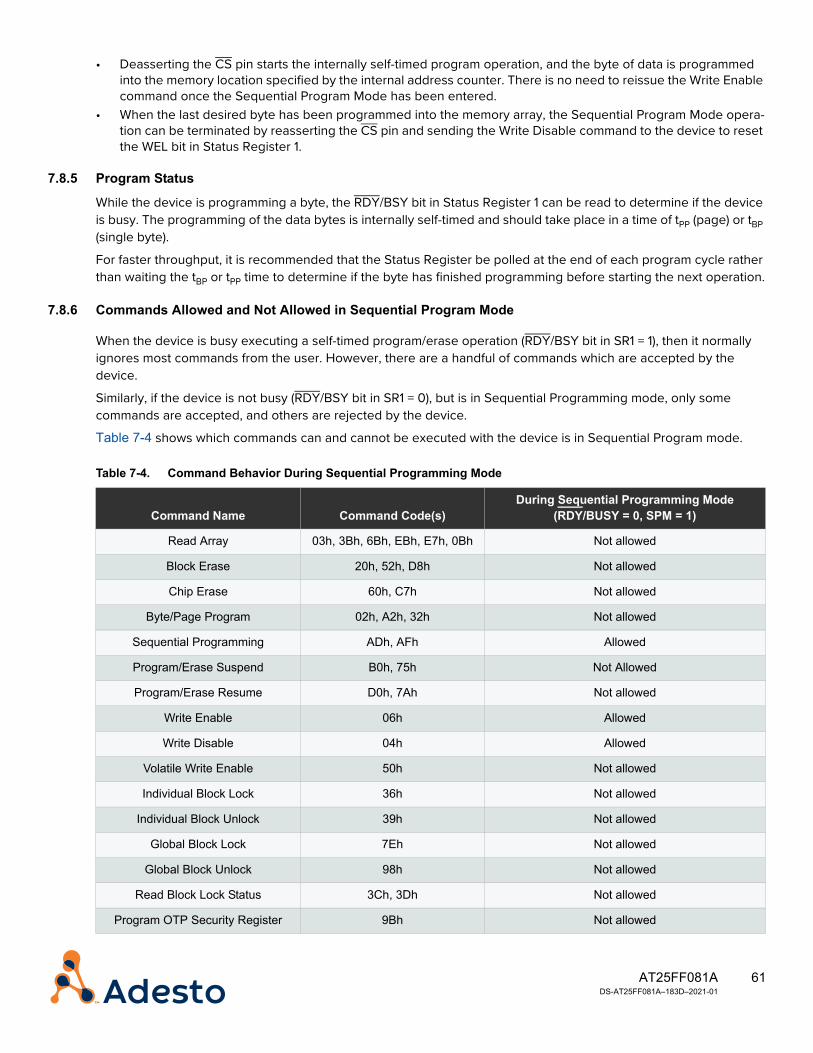
61AT25FF081A DS-AT25FF081A–183D–2021-01
• Deasserting the CS pin starts the internally self-timed program operation, and the byte of data is programmed into the memory location specified by the internal address counter. There is no need to reissue the Write Enable command once the Sequential Program Mode has been entered.
• When the last desired byte has been programmed into the memory array, the Sequential Program Mode opera-tion can be terminated by reasserting the CS pin and sending the Write Disable command to the device to reset the WEL bit in Status Register 1.
7.8.5 Program Status
While the device is programming a byte, the RDY/BSY bit in Status Register 1 can be read to determine if the device is busy. The programming of the data bytes is internally self-timed and should take place in a time of tPP (page) or tBP (single byte).
For faster throughput, it is recommended that the Status Register be polled at the end of each program cycle rather than waiting the tBP or tPP time to determine if the byte has finished programming before starting the next operation.
7.8.6 Commands Allowed and Not Allowed in Sequential Program Mode
When the device is busy executing a self-timed program/erase operation (RDY/BSY bit in SR1 = 1), then it normally ignores most commands from the user. However, there are a handful of commands which are accepted by the device.
Similarly, if the device is not busy (RDY/BSY bit in SR1 = 0), but is in Sequential Programming mode, only some commands are accepted, and others are rejected by the device.
Table 7-4 shows which commands can and cannot be executed with the device is in Sequential Program mode.
Table 7-4. Command Behavior During Sequential Programming Mode
Command Name Command Code(s)During Sequential Programming Mode
(RDY/BUSY = 0, SPM = 1)
Read Array 03h, 3Bh, 6Bh, EBh, E7h, 0Bh Not allowed
Block Erase 20h, 52h, D8h Not allowed
Chip Erase 60h, C7h Not allowed
Byte/Page Program 02h, A2h, 32h Not allowed
Sequential Programming ADh, AFh Allowed
Program/Erase Suspend B0h, 75h Not Allowed
Program/Erase Resume D0h, 7Ah Not allowed
Write Enable 06h Allowed
Write Disable 04h Allowed
Volatile Write Enable 50h Not allowed
Individual Block Lock 36h Not allowed
Individual Block Unlock 39h Not allowed
Global Block Lock 7Eh Not allowed
Global Block Unlock 98h Not allowed
Read Block Lock Status 3Ch, 3Dh Not allowed
Program OTP Security Register 9Bh Not allowed

62AT25FF081A DS-AT25FF081A–183D–2021-01
7.8.7 Programming Restrictions
The Sequential Program mode adheres to the following programming restrictions.
Multiple Data Bytes per Program Cycle If more than one byte of data is clocked in during a program cycle, then only the last byte of data sent on the SI pin is stored in the internal latches. The programming of each byte is internally self-timed and should take place in a time of tBP.
Deasserting the CS PinFor each program cycle, a complete byte of data must be clocked into the device before the CS pin is deasserted, and the CS pin must be deasserted on even byte boundaries (multiples of eight bits). Otherwise, the device abort the operation and the byte of data will not be programmed into the memory array. In addition, hardware resets the WEL bit in Status Register 1.
Protected MemoryIf the address initially specified by A[23:0] points to a memory location within a block that is in the protected state, then the Sequential Program Mode command will not be executed, and the device returns to the idle state once the CS pin has been deasserted. The WEL bit in the Status Register is also reset back to the logical “0” state.
Sequential Program mode does not automatically skip over protected blocks. Therefore, once the highest unprotected memory location in a programming sequence has been programmed, the device automatically exits the Sequential Program mode and resets the WEL bit in Status Register 1.
Read OTP Security Register 4Bh Not allowed
Read Status Registers (direct) 05h, 35h, 15h Allowed
Read Status Registers (indirect) 65h Allowed
Write Status Registers (direct) 01h, 31h, 11h Not allowed
Write Status Registers (indirect) 71h Not allowed
Status Register Lock 6Fh Not allowed
Terminate F0h Allowed
Enable Reset 66h Allowed
Reset Device 99h Allowed
Read Mfg ID and Device ID 9Fh, 90h, 94h Allowed
Deep Power Down B9h Not allowed
Resume from Deep Power Down ABh Not allowed
Ultra Deep Power Down 79h Not allowed
Read SFDP 5Ah Not allowed
Set Burst with Wrap 77h Not allowed
Table 7-4. Command Behavior During Sequential Programming Mode (continued)
Command Name Command Code(s)During Sequential Programming Mode
(RDY/BUSY = 0, SPM = 1)
63AT25FF081A DS-AT25FF081A–183D–2021-01
For example, if block 1 was protected and block 0 was currently being programmed, once the last byte of block 0 was programmed, the Sequential Program mode would automatically end. To continue programming with block 2, the Sequential Program mode would have to be restarted by supplying the ADh or AFh command, the three address bytes, and the first byte of block 2 to program.
Address WrappingThere is no address wrapping when using the Sequential Program Mode. Therefore, when the last byte (0FFFFFh) of the memory array has been programmed, the device automatically exits the Sequential Program mode and resets the WEL bit in Status Register 1.
64 KB Block AccessesIf during a Sequential Program operation, the address increments into a 64 KB block where an erase operation has been suspended, hardware will exit Sequential Program mode.
Clearing the WEL Bit in Status Register 1If the WEL bit in Status register 1 is cleared at any time during a sequential programming operation, hardware will exit Sequential Program mode.
7.8.8 Error Reporting
The device also incorporates an intelligent programming algorithm that can detect when a byte location fails to program properly. If a programming error arises, it is indicated by the EE and PE bits in Status Register 4.

64AT25FF081A DS-AT25FF081A–183D–2021-01
7.9 Dual Output Byte/Page Program (A2h)The Dual Output Byte/Page Program (A2h) command is similar to the standard Byte/Page Program command (02h) and can be used to program anywhere from a single byte of data up to 256 bytes of data into previously erased memory locations. Unlike the standard Byte/Page Program command, however, the Dual Output Byte/Page Program command allows two bits of data to be clocked into the device on every clock cycle rather than just one.
7.9.1 Command Prerequisites
Before the Dual Output Byte/Page Program command can be executed, the Write Enable command (06h) must have been previously issued to set the Write Enable Latch (WEL) bit in Status Register 1.
7.9.2 Transfer Format
The A2h command follows the 1-1-2 transfer format described in Section 5.3, where the command and address are transferred on the SI pin, and input data is transferred on the SI and SO pins. To facilitate this transfer, hardware switches the SO pin to an input as soon as the command has been decoded and the address transferred. Refer to Figure 5-9 for a timing diagram of this transaction.
7.9.3 Transfer Sequence
To perform a Dual Output Page Program operation, the CS pin is asserted and the information transferred as follows:• The A2h command is clocked into the device. Eight clocks are required to transfer the command. The most sig-
nificant bit of the command is transferred first.• Three address bytes are clocked in to specify the starting address location of the first byte to written. A total of
24 clocks are required to transfer the address. The most significant bit of the address (A[23]) is transferred first.• The first byte of data is transferred on the SI and SO pins. This requires four clock cycles. The data is always
input with the most significant bit on the SO pin during each clock as shown below. Like the standard Byte/Page Program command, all data clocked into the device is stored to an internal buffer.- First data clock: bit 7 is input on the SO pin- First data clock: bit 6 is input on the SI pin- Second data clock: bit 5 is input on the SO pin- Second data clock: bit 4 is input on the SI pin- Third data clock: bit 3 is input on the SO pin- Third data clock: bit 2 is input on the SI pin- Fourth data clock: bit 1 is input on the SO pin- Fourth data clock: bit 0 is input on the SI pin- Subsequent data bytes are transmitted in the same sequence as above
7.9.4 Program Status
While the device is programming a byte, Status Register 1 can be read to determine if the device is busy. The programming of the data bytes is internally self-timed and should take place in a time of tPP (page) or tBP (single byte).
For faster throughput, it is recommended that the Status Register be polled at the end of each program cycle rather than waiting the tBP or tPP time to determine if the byte has finished programming before starting the next operation.
7.9.5 Programming Restrictions
The Dual Output Byte/Page Program operation adheres to the following programming restrictions.
65AT25FF081A DS-AT25FF081A–183D–2021-01
Page Address BoundaryIf the starting memory address denoted by A[23:0] does not fall on a 256-byte page boundary (A[7:0] are not all 0), then special circumstances regarding which memory locations are to be programmed will apply. In this situation, any data sent to the device that exceeds the end of the page wraps around to the beginning of the same page.
Example: If the starting address denoted by A[23:0] is 0000FEh and three bytes of data are sent to the device, then the first two bytes of data is programmed at addresses 0000FEh and 0000FFh, while the last byte of data is programmed at address 000000h. The remaining bytes in the page (addresses 000001h through 0000FDh) will not be programmed and remain in the erased state (FFh).
Data TransfersWhen the CS pin is deasserted, the device programs the data stored in the internal buffer into the appropriate memory array locations based on the starting address specified by A[23:0] and the number of data bytes sent to the device. If fewer than 256 bytes of data is sent to the device, then the remaining bytes within the page will not be programmed and remains in the erased state (FFh). Conversely, if more than 256 bytes of data are sent to the device, then only the last 256 bytes sent are latched into the internal buffer.
Deassertion of the CS PinThe three address bytes and at least one complete byte of data must be clocked into the device before the CS pin can be deasserted. In addition, the CS pin must be deasserted on a byte boundary (multiple of eight bits). Otherwise, the device aborts the operation and no data is programmed into the memory array.
Protected MemoryIf the address specified by A[23:0] points to a memory location within a block that is in the protected state, then the Byte/Page Program command will not be executed and the device returns to the idle state once the CS pin has been deasserted. The WEL bit in the Status Register is reset back to the Logical 0 state if the program cycle is aborted
7.9.6 Error Reporting
The device incorporates an intelligent programming algorithm that can detect when a byte location fails to program properly. If a programming error arises, it is indicated by the EE and PE bits in Status Register 4.

66AT25FF081A DS-AT25FF081A–183D–2021-01
7.10 Quad Output Page Program (32h)The Quad Output Page Program command allows between 1 to 256 bytes of data to be programmed at previously erased memory locations.
7.10.1 Command Prerequisites
Before a Sequential Program command can be issued, the Write Enable (06h) command must have been previously issued to the device to set the WEL bit of Status Register 1. For more information on the QE bit, refer to Table 6.3, Status Register 1. In addition, the Quad Enable bit (QE bit in Status Register 2) must be set. For more information on the QE bit, refer to Table 6.4, Status Register 2.
7.10.2 Transfer Format
The 32h command follows the 1-1-4 transfer format described in Section 5.5, where the command and address are transferred on the SI pin, and data is transferred on the HOLD, WP, SO, and SI pins. Refer to Figure 5-11 for a timing diagram of this operation.
7.10.3 Transfer Sequence
To perform the Quad Output Page Program operation, the CS pin is asserted and the information transferred as follows:• The 32h command is clocked into the device. Eight clocks are required to transfer the command. The most sig-
nificant bit of the command is transferred first.• Three address bytes are clocked in to specify the starting address location of the first byte to read within the
memory array. A total of 24 clocks are required to transfer the address. The most significant bit of the address (A[23]) is transferred first.
• Following transfer of the last address byte, hardware switches the SO pin to an input.• Data is input on the HOLD, WP, SO, and SI pins. As a result, each byte transfer requires only two clock cycles to
complete. The data is always input with the most significant bit of the byte transferred first. The number of bytes transferred is determined by software. The transfer can be anywhere from a single byte to the entire memory array. Each data byte is shifted into the device as follows: - First data clock: bit 7 is input on the HOLD pin- First data clock: bit 6 is input on the WP pin- First data clock: bit 5 is input on the SO pin- First data clock: bit 4 is input on the SI pin- Second data clock: bit 3 is input on the HOLD pin- Second data clock: bit 2 is input on the WP pin- Second data clock: bit 1 is input on the SO pin- Second data clock: bit 0 is input on the SI pin- Additional data bytes are transferred on the four pins in the same manner as shown above.
7.10.4 Programming Restrictions
The Quad Output Byte/Page Program command adheres to the following programming restrictions• The CS pin must be deasserted on a byte boundary (multiples of eight bits). Otherwise, the device aborts the
operation and no action is taken.• If the memory is in a protected state, then the Byte/Page Program command will not be executed, and the
device returns to the idle state once the CS pin has been deasserted. • If the starting memory address denoted by A[23:0] does not fall on an even 256-byte page boundary (A[7:0] are
not all 0), then special circumstances regarding which memory locations to be programmed will apply. In this sit-uation, any data sent to the device that exceeds the page size wraps around back to the beginning of the same page.
67AT25FF081A DS-AT25FF081A–183D–2021-01
For example, if the starting address denoted by A23-A0 is 0000FEh, and three bytes of data are sent to the device, then the first two bytes of data is programmed at addresses 0000FEh and 0000FFh while the last byte of data is programmed at address 000000h. The remaining bytes in the page (addresses 000001h through 0000FDh) will not be programmed and remain in the current state. In addition, if more than 256 bytes of data are sent to the device, then only the last 256 bytes sent are latched into the internal buffer.
• If the device receives either an incomplete address, or an incomplete data byte, the operation is aborted and hardware clears the WEL bit is Status Register 1.
7.10.5 Error Reporting
The device also incorporates an intelligent programming algorithm that can detect when a byte location fails to program properly. If a programming error arises, it is indicated by the EE and PE bits in Status Register 4.
68AT25FF081A DS-AT25FF081A–183D–2021-01
7.11 Program/Erase Suspend (75h/B0h)The device supports two Program/Erase Suspend commands, 75h and B0h, that perform the exact same function. The 75h command can be used for legacy software, and the B0h command is used for compatibility with future implementations.
In some code plus data storage applications, it is often necessary to process certain high-level system interrupts that require relatively immediate reading of code or data from the Flash memory. In such an instance, it may not be possible for the system to wait the microseconds or milliseconds required for the Flash memory to complete a program or erase cycle. The Program/Erase Suspend command allows a program or erase operation in progress to be suspended so that other device operations can be performed. For example, by suspending an erase operation to a particular block, the system can perform functions such as a program or read to a different block.
7.11.1 Command Prerequisites
None.
7.11.2 Transfer Format
The 75h and B0h commands follow the 1-0-0 transfer format described in Section 5.2, where the command is transferred on the SI pin. No address or data are transferred for this command. Refer to Figure 5-1 for a timing diagram of this operation.
7.11.3 Transfer Sequence
To perform the Program Erase/Suspend operation, the CS pin is asserted and the information transferred as follows:• The 75h or B0h command is clocked into the device. Eight clocks are required to transfer the command. The
most significant bit of the command is transferred first.• When the CS pin is deasserted, the device suspends the program. Refer to Table 7-1 for more information on the transfer sequence for this command.
7.11.4 Command Behavior During a Program/Erase Operation
If an attempt is made to perform an operation that is not allowed during a program or erase suspend, such as a Write Status Register operation, then the device simply ignores the command and no operation is performed. The state of the WEL bit in Status Register 1 is not affected. Note that in the table below, the RDY/BSY bit is located in Status Register 1. The PS and ES bits are located in Status Register 5.
Table 7-5. Command Behavior During Program/Erase or Program/Erase Suspend Operations
CommandCommand
Code(s)
During Program or Erase(RDY/BSY = 1, PS = x,
ES = x)
During Program Suspend(RDY/BSY = 0, PS = 1,
ES = x)
During Erase Suspend(RDY/BSY = 0, PS = 0,
ES = 1)
Read Array 03h, 0Bh, 3Bh, 6Bh, EBh, E7h Not allowed Allowed Allowed
Block Erase 20h, 52h, D8h Not allowed Not allowed Not allowed
Chip Erase 60h, C7h Not allowed Not allowed Not allowed
Byte/Page Program 02h, A2h, 32h Not allowed Not allowed Allowed (1)
Sequential Programming ADh, AFh Not allowed Not allowed Allowed(1)
Program/Erase Suspend B0h, 75h Allowed Not allowed Not allowed
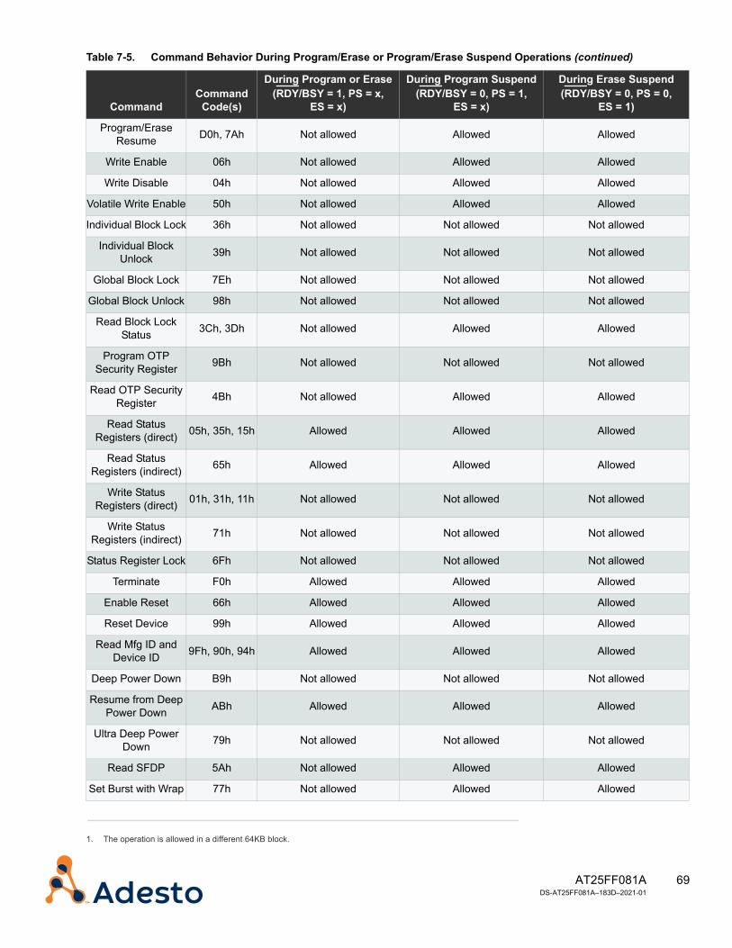
69AT25FF081A DS-AT25FF081A–183D–2021-01
Program/Erase Resume D0h, 7Ah Not allowed Allowed Allowed
Write Enable 06h Not allowed Allowed Allowed
Write Disable 04h Not allowed Allowed Allowed
Volatile Write Enable 50h Not allowed Allowed Allowed
Individual Block Lock 36h Not allowed Not allowed Not allowed
Individual Block Unlock 39h Not allowed Not allowed Not allowed
Global Block Lock 7Eh Not allowed Not allowed Not allowed
Global Block Unlock 98h Not allowed Not allowed Not allowed
Read Block Lock Status 3Ch, 3Dh Not allowed Allowed Allowed
Program OTP Security Register 9Bh Not allowed Not allowed Not allowed
Read OTP Security Register 4Bh Not allowed Allowed Allowed
Read Status Registers (direct) 05h, 35h, 15h Allowed Allowed Allowed
Read Status Registers (indirect) 65h Allowed Allowed Allowed
Write Status Registers (direct) 01h, 31h, 11h Not allowed Not allowed Not allowed
Write Status Registers (indirect) 71h Not allowed Not allowed Not allowed
Status Register Lock 6Fh Not allowed Not allowed Not allowed
Terminate F0h Allowed Allowed Allowed
Enable Reset 66h Allowed Allowed Allowed
Reset Device 99h Allowed Allowed Allowed
Read Mfg ID and Device ID 9Fh, 90h, 94h Allowed Allowed Allowed
Deep Power Down B9h Not allowed Not allowed Not allowed
Resume from Deep Power Down ABh Allowed Allowed Allowed
Ultra Deep Power Down 79h Not allowed Not allowed Not allowed
Read SFDP 5Ah Not allowed Allowed Allowed
Set Burst with Wrap 77h Not allowed Allowed Allowed
1. The operation is allowed in a different 64KB block.
Table 7-5. Command Behavior During Program/Erase or Program/Erase Suspend Operations (continued)
CommandCommand
Code(s)
During Program or Erase(RDY/BSY = 1, PS = x,
ES = x)
During Program Suspend(RDY/BSY = 0, PS = 1,
ES = x)
During Erase Suspend(RDY/BSY = 0, PS = 0,
ES = 1)
70AT25FF081A DS-AT25FF081A–183D–2021-01
7.11.5 Device Status
When the CS pin is deasserted, the program or erase operation currently in progress suspends within a time of tSUSE. Hardware sets the Suspend (SUSP) bit in Status Register 2 and the ES or PS bits in Status Register 5 to indicate that the program or erase operation has been suspended. In addition, hardware clears the RDY/BSY bit in Status Register 1 to indicate that the device is ready for another operation.
7.11.6 Programming Restrictions
The Erase/Program Suspend command adheres to the following programming restrictions.
The following commands cannot be suspended:• Write Status Register 1 (01h)• Write Status Register 2 (31h)• Write Status Register 3 (11h)• Write Status Registers (71h)• Status Register Lock (6Fh)• Program OTP Security Registers (9Bh)• Chip Erase (60h/C7h)• Sequential Programming (AFh/ADh)
Hardware ignores the Program/Suspend command if it is issued while these commands are in progress.
Erase Suspend and Program Suspend OrderingA program operation can be performed while an erase operation is suspended. However, that operation must be completed before the erase operation can be resumed. In addition, an erase operation cannot be performed while a program operation is suspended. Other device operations, such as a Read Status Register, can also be performed while a program or erase operation is suspended.
Write Enable Latch IgnoredSince the need to suspend a program or erase operation is immediate, the Write Enable command does not need to be issued prior to the Program/Erase Suspend command being issued. Therefore, the Program/Erase Suspend command operates independently of the state of the WEL bit in the Status Register.
Deasserting the CS PinThe complete command must be clocked into the device before the CS pin is deasserted. In addition, the CS pin must be deasserted on a byte boundary (multiples of eight bits). Otherwise, no suspend operation is performed.
Accessing a Suspended AreaIf a read operation is attempted to a suspended area (page for programming or block for erasing), then the device outputs undefined data. Therefore, when performing a Read Array operation to an unsuspended area and the device's internal address counter increments and crosses into the suspended area, the device starts outputting undefined data until the internal address counter crosses to an unsuspended area.
71AT25FF081A DS-AT25FF081A–183D–2021-01
7.12 Program/Erase Resume (7Ah/D0h)The device supports two Program/Erase Resume commands, 7Ah and D0h, that perform the exact same function. The 7Ah command can be used for legacy software, and the D0h command is used for compatibility with future implementations.
The Program/Erase Resume command allows a suspended program or erase operation to be resumed and continue programming a Flash page or erasing a Flash memory block where it left off.
7.12.1 Command Prerequisites
Hardware accepts the Program/Erase Resume command only if the ES bit (set when an erase operation is suspended) or PS bit (set when a program operation is suspended) in Status Register 5 is set and the RDY/BSY bit in Status Register 1 is cleared. If the ES/PS bit is cleared or the RDY/BSY bit is set, the Program/Erase Resume command is ignored by the device. Refer to Table 6.3, Status Register 1 and Table 6.7, Status Register 5.
Note that the Write Enable command does not need to be issued prior to the Program/Erase Resume command being issued. Therefore, the Program/Erase Resume command operates independently of the state of the WEL bit in Status Register 1.
7.12.2 Transfer Format
The 7Ah and D0h commands follow the 1-0-0 transfer format described in Section 5.2, where the command is transferred on the SI pin. No address or data are transferred for this command. Refer to Figure 5-1 for a timing diagram of this operation.
7.12.3 Transfer Sequence
To perform the Program/Erase Resume operation, the CS pin is asserted and the information transferred as follows:• The 7Ah or D0h command is clocked into the device. Eight clocks are required to transfer the command. The
most significant bit of the command is transferred first. No address of data are required for this command.• When the CS pin is deasserted, the device resumes the program. Refer to Table 7-1 for more information on the transfer sequence for this command.
7.12.4 Command Behavior
When the command is executed, hardware performs the following:• Hardware clears either the PS or the ES bits in Status Register 5 depending on whether a program or erase
operation has been suspended. If both of these bits are cleared, hardware clears the SUSP bit in Status Register 2.
• Hardware sets the RDY/BSY bit in Status Register 1 to indicate that the device is busy. • When the CS pin is deasserted, the program or erase operation currently suspended resumes within a time of
tRES.
7.12.5 Programming Restrictions
The Program/Erase Resume command adheres to the following programming restrictions.• The complete command must be clocked into the device before the CS pin is deasserted.• The CS pin must be deasserted on a byte boundary (multiples of eight bits). Otherwise, no resume operation is
performed.• While the device is busy resuming a program or erase operation, any attempts at issuing the Program/Erase
Suspend command are ignored. Therefore, if a resumed program or erase operation needs to be subsequently suspended again, the system must either wait the entire tRES time before issuing the Program/Erase Suspend command, or it can check the status of the RDY/BSY bit in Status Register 1, or the ES/PS bits in Status Register 5 to determine if the previously suspended program or erase operation has resumed.

72AT25FF081A DS-AT25FF081A–183D–2021-01
• During a simultaneous Erase Suspend/Program Suspend condition, issuing the Program/Erase Resume com-mand results in the program operation resuming first. After the program operation has been completed, the Pro-gram/Erase Resume command must be issued again in order for the erase operation to be resumed. For more information, refer to Section 5.10.1, Nested Operations.

73AT25FF081A DS-AT25FF081A–183D–2021-01
7.13 Set Burst Wrap (77h)The Set Burst with Wrap (77h) command is used in conjunction with the EBh and E7h commands to support a cache line fill, regardless of the starting address. This type of operation, known as ‘address wrapping’, is an MCU-friendly feature that allows the Microcontroller Unit (MCU) cache controller to fill a cache line in one operation starting from a specific address (known as the critical byte) within the cache line, proceeding to the end of the line, then wrapping around the start of the cache line to complete the fill.
For example, if the wrap size is 16 bytes and the starting address is 0x1004, then the read sequence would be as follows: 0x1004, 0x1005, 0x1006, 0x1007, 0x1008, 0x1009, 0x100A, 0x100B, 0x100C, 0x100D, 0x100E, 0x100F, 0x1000, 0x1001, 0x1002, 0x1003. As shown in this sequence, the fill starts at address 0x1004, proceeds to the end of the cache line (0x100F), then wraps around to 0x1000 to complete the fill.
The wrap feature can improve code execution performance in the MCU system, as the MCU will first receive the command or data it requires at that instant, and then fetch the remainder of the cache line without requiring additional commands or addresses to be sent.
The 77h command is used to both enable/disable the wrap-around feature, and determine the size of the wrap. The 77h command sets the state of bits W6, W5, and W4 as shown in Table 7-6.
7.13.1 Command Prerequisites
None.
7.13.2 Transfer Format
The 77h command follows the 1-4-4 transfer format described in Section 5.6, where the command is transferred on the SI pin, and the address and data are transferred on the HOLD, WP, SO, and SI pins. Refer to Figure 5-15 for a timing diagram of this command.
7.13.3 Transfer Sequence
To perform the Set Burst with Wrap operation, the CS pin is asserted and the information transferred as follows:• The 77h command is clocked into the device. Eight clocks are required to transfer the command. The most sig-
nificant bit of the command is transferred first.• Three address bytes are clocked in. A total of 6 clocks are required to transfer the address. The most significant
bit of the address (A[23]) is transferred first. Even though the address must be clocked in, the address is treated as a don’t care field internally.
• Following transfer of the last address byte, eight Wrap bits are transferred which indicate the length of the wrap operation as described in the table below.
7.13.4 Wrap Bits
After the last address byte is transferred, the device transfers eight wrap bits (W7-0), which indicate the wrap length. Note that only wrap bits W6:W4 are used during this operation. The W7 and W3:W0 bits are not used. This is shown in the following table.
Table 7-6. Encoding of Burst Wrap Bits
W6 W5W4 = 0 W4 = 1
Wrap Length Wrap Around Wrap Length Wrap Around0 0 8-byte Yes N/A No
0 1 16-byte Yes N/A No
1 0 32-byte Yes N/A No
1 1 64-byte Yes N/A No
74AT25FF081A DS-AT25FF081A–183D–2021-01
Once the 77h command is executed and the W6:W4 bits are set, the subsequent EBh or E7h command uses these bits to determine what section size to access within a given page. As shown in the table, returning to the normal read operation requires the execution of another 77h command with the W4 bit driven high (W4 = 1).
7.13.5 Programming Restrictions
The Set Burst with Wrap command adheres to the following programming restrictions.• The CS pin must be deasserted on a byte boundary (multiples of eight bits). Otherwise, the device aborts the
operation and no action is taken.
75AT25FF081A DS-AT25FF081A–183D–2021-01
7.14 Write Enable (06h)The Write Enable command is used to set the Write Enable Latch (WEL) bit in Status Register 1. The WEL bit must be set for any of the following commands to be executed:• Byte/Page Program (02h)• Dual Output Byte/Page Program (A2h)• Quad Output Byte/Page Program (32h)• Sequential Program Mode (AFh/ADh)• Any Erase command (20h, 52h, D8h, 60h/C7h)• Program OTP Security Register (9Bh)• Write Status Register (01h, 31h, 11h, 71h)This makes the issuance of the above commands a two step process, thereby reducing the chances of a command being accidentally or erroneously executed. If the WEL bit in the Status Register is not set prior to the issuance of one of these commands, that command will not be executed.
7.14.1 Command Prerequisites
None.
7.14.2 Transfer Format
The 06h command follows the 1-0-0 transfer format described in Section 5.2, where the command is transferred on the SI pin. No address or data are transferred for this command. Refer to Figure 5-1 for a timing diagram of this operation.
7.14.3 Transfer Sequence
To perform the Write Enable operation, the CS pin is asserted and the information transferred as follows:• The 06h command is clocked into the device. Eight clocks are required to transfer the command. The most sig-
nificant bit of the command is transferred first. No address or data are required for this command.• When the CS pin is deasserted, hardware sets the WEL bit in Status Register 1. Refer to Table 7-1 for more information on the transfer sequence for this command.
7.14.4 Programming Restrictions
The Write Enable command adheres to the following programming restrictions.• The complete command must be clocked into the device before the CS pin is deasserted.• The CS pin must be deasserted on a byte boundary (multiple of eight bits). Otherwise, the device aborts the
operation and no action is taken.
76AT25FF081A DS-AT25FF081A–183D–2021-01
7.15 Write Disable (04h)The Write Disable command is used to clear the Write Enable Latch (WEL) bit in Status Register 1. When the WEL bit is cleared, the following commands cannot be executed:• Byte/Page Program (02h)• Dual Output Byte/Page Program (A2h)• Quad Output Byte/Page Program (32h)• Sequential Program Mode (AFh/ADh)• Any Erase command (20h, 52h, D8h, 60h/C7h)• Program OTP Security Register (9Bh)• Write Status Register (01h, 31h, 11h, 71h)Other conditions can also cause the WEL bit to be cleared. For more information, refer to Section 6-2, Status Register 1 Format.
7.15.1 Command Prerequisites
None.
7.15.2 Transfer Format
The 04h command follows the 1-0-0 transfer format described in Section 5.2, where the command is transferred on the SI pin. No address or data are transferred for this command. Refer to Figure 5-1 for a timing diagram of this operation.
7.15.3 Transfer Sequence
To perform the Write Disable operation, the CS pin is asserted and the information transferred as follows:• The 04h command is clocked into the device. Eight clocks are required to transfer the command. The most sig-
nificant bit of the command is transferred first. No address or data are required for this command.• When the CS pin is deasserted, hardware clears the WEL bit in Status Register 1. Refer to Table 7-1 for more information on the transfer sequence for this command.
7.15.4 Programming Restrictions
The Write Disable command adheres to the following programming restrictions.• The complete command must be clocked into the device before the CS pin is deasserted.• The CS pin must be deasserted on a byte boundary (multiple of eight bits). Otherwise, the device aborts the
operation and no action is taken.
77AT25FF081A DS-AT25FF081A–183D–2021-01
7.16 Volatile Status Register Write Enable (50h)To write the volatile version of the Status Register bits, the Write Enable for Volatile Status Register (50h) command must be issued prior to each Write Status Register (01h) command. The Write Enable for the Volatile Status Register command does not set the Write Enable Latch (WEL) bit in Status Register 1. It is only valid for the next following Write Status Register command, to change the volatile Status Register bit values.
7.16.1 Command Prerequisites
None.
7.16.2 Transfer Format
The 50h command follows the 1-0-0 transfer format described in Section 5.2, where the command is transferred on the SI pin. No address or data are transferred for this command. Refer to Figure 5-1 for a timing diagram of this operation.
7.16.3 Transfer Sequence
To perform the Write Disable operation, the CS pin is asserted and the information transferred as follows:• The 50h command is clocked into the device. Eight clocks are required to transfer the command. The most sig-
nificant bit of the command is transferred first. No address or data are required for this command.• When the CS pin is deasserted, hardware performs the operation. Refer to Table 7-1 for more information on the transfer sequence for this command.
7.16.4 Programming Restrictions
The Volatile Status Register Write Enable command adheres to the following programming restrictions.• The complete command must be clocked into the device before the CS pin is deasserted.• The CS pin must be deasserted on a byte boundary (multiple of eight bits). Otherwise, the device aborts the
operation and no action is taken.
78AT25FF081A DS-AT25FF081A–183D–2021-01
7.17 Individual Block Lock (36h)The Individual Block Lock command can be used to protect individual pages in the memory array from being programmed or erased via one of the Program or Erase commands. To enable the individual block lock function, the WPS bit in Status Register 3 must be set. If the WPS bit is cleared, write protection is then determined by the combination of the CMPRT, BPSIZE, TB, and BP[2:0] bits in the Status Register 1. The default value for each individual lock bit is 1 at power-up or reset, so the entire memory array is protected.
7.17.1 Command Prerequisites
The Write Enable (06h) command must be executed before the device can accept the Individual Block Lock command. This is required to set the WEL bit in Status Register 1.
7.17.2 Transfer Format
The 36h command follows the 1-1-0 transfer format described in Section 5.2, where the command and address are transferred on the SI pin. The address represents the individual block to be locked. Hence no data is transferred for this command.
7.17.3 Transfer Sequence
To perform the Individual Block Lock operation, the CS pin is asserted and the information transferred as follows:• The 36h command is clocked into the device. Eight clocks are required to transfer the command. The most sig-
nificant bit of the command is transferred first.• Three address bytes are clocked in to specify the address location to be locked within the memory array. A total
of 24 clocks are required to transfer the address. The most significant bit of the address (A[23]) is transferred first.
• When the CS pin is deasserted, hardware performs the operation and clears the WEL bit in Status Register 1. Refer to Table 7-1 for more information on the transfer sequence for this command.
7.17.4 Programming Restrictions
The Individual Block Lock command adheres to the following programming restrictions.• The complete command must be clocked into the device before the CS pin is deasserted.• The CS pin must be deasserted on a byte boundary (multiple of eight bits). Otherwise, the device aborts the
operation and no action is taken.
79AT25FF081A DS-AT25FF081A–183D–2021-01
7.18 Individual Block Unlock (39h)The Individual Block Unlock command can be used to unlock individual pages in the memory array to allow them to be programmed or erased via one of the Program or Erase commands. To enable the individual block unlock function, the WPS bit in Status Register 3 must be set. If WPS is cleared, write protection is then determined by the combination of the CMP, SEC, TB, and BP[2:0] bits in Status Register 1. The default value for each individual lock bit is 1 at power-up or reset, so the entire memory array is being protected.
7.18.1 Command Prerequisites
The Write Enable (06h) command must be executed before the device can accept the Individual Block Unlock command. This is required to set the WEL bit in Status Register 1.
7.18.2 Transfer Format
The 39h command follows the 1-1-0 transfer format described in Section 5.2, where the command and address are transferred on the SI pin. The address represents the individual block to be unlocked. Hence no data is transferred for this command. Refer to Figure 5-2, SPI Transfer — Command and Address Only for a timing diagram of this transaction.
7.18.3 Transfer Sequence
To perform the individual block unlock operation, the CS pin is asserted and the information transferred as follows:• The 39h command is clocked into the device. Eight clocks are required to transfer the command. The most sig-
nificant bit of the command is transferred first.• Three address bytes are clocked in to specify the address location to be unlocked within the memory array. A
total of 24 clocks are required to transfer the address. The most significant bit of the address (A[23]) is trans-ferred first.
• When the CS pin is deasserted, hardware performs the operation and clears the WEL bit in Status Register 1. Refer to Table 7-1 for more information on the transfer sequence for this command.
7.18.4 Programming Restrictions
The Individual Block Unlock command adheres to the following programming restrictions.• The complete command must be clocked into the device before the CS pin is deasserted.• The CS pin must be deasserted on a byte boundary (multiple of eight bits). Otherwise, the device aborts the
operation and no action is taken.
80AT25FF081A DS-AT25FF081A–183D–2021-01
7.19 Read Block Lock (3Ch/3Dh)The Read Block Lock commands allow the user to read the status of the lock bits in each block. The individual block locks are used to protect any individual block. The default value for all individual block lock bits is 1 upon device power on or after reset.
The 3Ch and 3Dh commands perform the exact same operation. These two commands are identical and are provided for backward compatibility purposes.
7.19.1 Command Prerequisites
The WPS bit in Status Register 3 must be set. When WPS is set, software uses the Block Lock (36h) and Block Unlock (39h) commands to lock and unlock blocks of memory. If the WPS bit is cleared, write protection is determined by the combination of CMP, SEC, TB, BP[2:0] bits in the Status Registers. The Read Block Lock command must not be used to determine the protection status of any region of the memory. Refer to Section 5.8.1 for more information on the protection scheme.
7.19.2 Transfer Format
The 3Ch and 3Dh commands follow the 1-1-1 transfer format described in Section 5.2, where the command and address are transferred on the SI pin, and data is transferred on the SO pin. Figure 5-5, SPI Transfer — Command, Address, and Data — Read Operation with No Dummy Bytes shows a timing diagram for this transaction.
7.19.3 Transfer Sequence
To perform the Read Block Lock operation, the CS pin is asserted and the information transferred as follows:• The 3dh or 3Dh command is clocked into the device. Eight clocks are required to transfer the command. The
most significant bit of the command is transferred first.• Three address bytes are clocked in to specify the starting address location of the first byte to read within the
buffer. A total of 24 clocks are required to transfer the address. The most significant bit of the address (A[23]) is transferred first.
• Data is output on the SO pin and requires eight clock cycles. The MSB of the lock value is driven onto the SO pin first, and the LSB is driven out last. If the LSB is 1, the corresponding block is locked and no erase or program opera-tion can be executed to that block. If the LSB is 0, the block is unlocked, indicating that program/erase operations are allowed. The remaining bits 7:1 of this value are undefined. If CS is kept low and additional data is clocked out, the device simply repeats the same byte over and over again until CS goes high. Out of the 8 bits in this byte, the LSB (bit 0) has the lock bit information, the rest of the are undefined. The lock bit information corresponds to the region of memory that encapsulates the 20-bit address provided by the user. So for example:- If the user provides an address of 0x000000, the device returns the lock status of the 4KB region from
0x000000 - 0x000FFF.- If the user provides an address of 0x001234, the device returns the lock status of the 4KB region 0x001000 -
0x001FFF.
7.19.4 Programming Restrictions
The Read Block Lock command adheres to the following programming restrictions.• The complete command must be clocked into the device before the CS pin is deasserted.

81AT25FF081A DS-AT25FF081A–183D–2021-01
7.20 Global Block Lock (7Eh)The Global Block Lock command is used to set all of the block bits to 1 with one operation.
7.20.1 Command Prerequisites
The Write Enable command (06h) must be executed to set WEL bit in Status Register 1 before the Global Block Lock command can be executed. Refer to Section 7.14, Write Enable (06h) for more information.
7.20.2 Transfer Format
The 7Eh command follows the 1-0-0 transfer format described in Section 5.2, where the command is transferred on the SI pin. No address or data are transferred for this command. Refer to Figure 5-1 for a timing diagram of this operation.
7.20.3 Transfer Sequence
To perform the Global Block Lock operation, the CS pin is asserted and the information transferred as follows:• The 7Eh command is clocked into the device. Eight clocks are required to transfer the command. The most sig-
nificant bit of the command is transferred first. No address or data are required for this command.• When the CS pin is deasserted, hardware performs the operation and clears the WEL bit in Status Register 1. Refer to Table 7-1 for more information on the transfer sequence for this command.
7.20.4 Programming Restrictions
The Global Block Lock command adheres to the following programming restrictions.• The complete command must be clocked into the device before the CS pin is deasserted.• The CS pin must be deasserted on a byte boundary (multiple of eight bits). Otherwise, the device aborts the
operation and no action is taken.
82AT25FF081A DS-AT25FF081A–183D–2021-01
7.21 Global Block Unlock (98h)The Global Block UnLock command is used to reset all of the block bits to 0 with one operation.
7.21.1 Command Prerequisites
The Write Enable command (06h) must be executed to set WEL bit in Status Register 1 before the Global Block Unlock command can be executed. Refer to Section 7.14, Write Enable (06h) for more information.
7.21.2 Transfer Format
The 98h command follows the 1-0-0 transfer format described in Section 5.2, where the command is transferred on the SI pin. No address or data are transferred for this command. Refer to Figure 5-1 for a timing diagram of this operation.
7.21.3 Transfer Sequence
To perform the Global Block Unlock operation, the CS pin is asserted and the information transferred as follows:• The 98h command is clocked into the device. Eight clocks are required to transfer the command. The most sig-
nificant bit of the command is transferred first. Since all blocks are unlocked with this command, no address or data are required.
• When the CS pin is deasserted, hardware performs the operation and clears the WEL bit in Status Register 1. Refer to Table 7-1 for more information on the transfer sequence for this command
7.21.4 Programming Restrictions
The Global Block Unlock command adheres to the following programming restrictions.• The complete command must be clocked into the device before the CS pin is deasserted.• The CS pin must be deasserted on a byte boundary (multiple of eight bits). Otherwise, the device aborts the
operation and no action is taken.
83AT25FF081A DS-AT25FF081A–183D–2021-01
7.22 Program Security Register (9Bh)There are four specialized 128-byte OTP (One-Time Programmable) Security Registers that can be used for purposes such as unique device serialization and locked key storage.
7.22.1 Command Prerequisites
Before the Program OTP Security Register command can be issued, the Write Enable command (06h) must be executed to set WEL bit in Status Register 1. Refer to Section 7.14, Write Enable (06h) for more information.
7.22.2 OTP Security Register Layout
The OTP Security Registers are independent of the main Flash memory array. The four registers are organized as follows:
7.22.3 Transfer Format
The 9Bh command follows the 1-1-1 transfer format described in Section 5.2, where the command and address are transferred on the SI pin, and data is transferred on the SO pin. Refer to Figure 5-7 for timing diagram of this transfer.
7.22.4 Transfer Sequence
To perform the Program OTP Register operation, the CS pin is asserted and the information transferred as follows:• The 9Bh command is clocked into the device. Eight clocks are required to transfer the command. The most sig-
nificant bit of the command is transferred first.• Three address bytes are clocked in to specify the starting address location of the first byte to read within the
memory array. A total of 24 clocks are required to transfer the address. The most significant bit of the address (A[23]) is transferred first. For this command, address bits 23:9 are don’t care. Only bits 8:0 are used to address the appropriate Security register. Refer to Table 7-11 for an encoding of the address.
Table 7-7. OTP Security Register 0 Bit Assignments
Security Register Byte Number
127 126 125 ..... 2 1 0
Factory Programmed by Adesto
Table 7-8. OTP Security Register 1 Bit Assignments
Security Register Byte Number
255 254 253 ..... 130 129 128
User Security OTP Register
Table 7-9. OTP Security Register 2 Bit Assignments
Security Register Byte Number
383 382 381 ..... 258 257 256
User Security OTP Register
Table 7-10. OTP Security Register 3 Bit Assignments
Security Register Byte Number
511 510 509 ..... 386 385 384
User Security OTP Register
84AT25FF081A DS-AT25FF081A–183D–2021-01
• Data is input on the SI pin. Each byte transfer requires eight clock cycles. The data is always input with the most significant bit of the byte transferred first. The number of bytes transferred is determined by software. The trans-fer can be anywhere from a single byte to the entire OTP register array. Additional data bytes are transferred every eight clocks as long as the CS pin is asserted. The programming of the data bytes is internally self-timed and takes place in a time of tOTPP if the entire 128-byte register is programmed at once.
• When the CS pin is deasserted, the device takes the data stored in the internal buffer and programs it into the appropriate OTP Security Register locations based on the starting address specified by A8-A0 and the number of data bytes sent to the device.
Note that the Program OTP Security Register command utilizes an internal 256-buffer for processing. Therefore, the contents of the buffer is altered from its previous state when this command is issued.
Refer to Table 7-1 for more information on the transfer sequence for this command.
7.22.5 Addressing the OTP Security Registers
Each byte within the four OTP security registers can be accessed using bits 8:0 of the address. Bits 23:9 of the address are ignored. The lower 7 bits (6:0) are used to select a byte within a given 128-byte OTP register. The next two bits (8:7) are used to select one of the four OTP registers. This is shown in Figure 7-11.
7.22.6 Programming Status
While the device is programming the OTP Security Register, the RDY/BSY bit in Status Register 1 can be read to determine if the operation is still in progress. For faster throughput, it is recommended that the Status Register be polled rather than waiting the tOTPP time to determine if the data bytes have finished programming. At some point before the OTP Security Register programming completes, hardware clears the WEL bit in the Status Register.
7.22.7 Locking OTP Registers 1 - 3
The tables above show the bytes associated with each OTP register. OTP register 0 is locked by default as the value is programmed by Adesto at the factory and cannot be changed. For OTP registers 1 - 3, the most significant byte is as follows:• OTP Register 1: MSB = byte 255• OTP Register 2: MSB = byte 383• OTP Register 3: MSB = byte 511For OTP registers 1 - 3, bit-level programming is allowed for the first 127 bytes of the registers. However, the register is locked whenever one or more bits of the most significant byte are programmed. For example, if any bit of byte 255 in OTP register 1 is programmed, that register is locked by hardware can cannot be programmed further.
Table 7-11. OTP Register Access Address Map
Address
23:9 A8 A7 A6 A5 A4 A3 A2 A1 A0
Don’t care 0 0 OTP Security Register 0 (Factory Programmed by Adesto)
A[6:0] = 0000000 - byte 0, A[6:0] = 1111111 - byte 127
Don’t care 0 1 User defined OTP Security Register 1
A[6:0] = 0000000 - byte 128, A[6:0] = 1111111 - byte 255
Don’t care 1 0 User defined OTP Security Register 2
A[6:0] = 0000000 - byte 256, A[6:0] = 1111111 - byte 383
Don’t care 1 1 User defined OTP Security Register 3
A[6:0] = 0000000 - byte 384, A[6:0] = 1111111 - byte 511

85AT25FF081A DS-AT25FF081A–183D–2021-01
7.22.8 Verifying the Locked Status of a Security Register
As described in the previous subsection, once any bit in the MSB of Security registers 1 - 3 is written, the register is locked and not further programming is allowed. Software can determine the Locked status of each register by reading bits 5:3 (SL3:SL1) of Status Register 2. Each bit corresponds to one of the user defined OTP security registers. If the corresponding bit is cleared, the register is not locked. If the corresponding bit is set, the register is locked and cannot be programmed. Refer to Section 6.4, Status Register 2 for more information.
7.22.9 Programming Restrictions
The Program OTP Register command adheres to the following program restrictions.
Early Power DownIf the device is powered-down during the OTP Security Register program cycle, then the contents of the 128-byte user programmable portion of the OTP Security Register cannot be guaranteed and may not be programmed again.
Deasserting the CS PinThe CS pin must be deasserted on a byte boundary (multiples of eight bits). Otherwise, the device aborts the operation and the user-programmable portion of the OTP Security Register is not programmed.
Incomplete Address or DataThe WEL bit in the Status Register is cleared if the OTP Security Register program cycle aborts due to an incomplete address being sent or an incomplete byte of data being sent.
Register Previously ProgrammedPrior to programming an OTP register, hardware checks the state of the SL3:1 field in Status Register 2. For example, if an attempt is made to program OTP register 1, and the register was previously programmed as indicated by the SL1 bit in Status Register 2 being set, the operation is aborted.
86AT25FF081A DS-AT25FF081A–183D–2021-01
7.23 Read OTP Security Register (4Bh)The Read OTP Security Register command accesses the four specialized OTP security registers. Any portion of the value can be read out depending on when the CS pin is deasserted.
7.23.1 Command Prerequisites
None.
7.23.2 Transfer Format
The 4Bh command follows the 1-1-1 transfer format described in Section 5.2, where the command and address are transferred on the SI pin, and data is transferred on the SO pin. Refer to Figure 5-5 for a timing diagram of this transaction. In this diagram a single byte of data is shown.
7.23.3 Transfer Sequence — Single Register
To perform the Read OTP Security register operation of a single register, the CS pin is asserted and the information transferred as follows:• The 4Bh command is clocked into the device. Eight clocks are required to transfer the command. The most sig-
nificant bit of the command is transferred first.• Three address bytes are clocked in to specify the starting address location of the first byte to read within the
memory array. A total of 24 clocks are required to transfer the address. The most significant bit of the address (A[23]) is transferred first. The address breakdown is as follows:- A[23:9] are don’t care- A[8:0] indicate the byte address
• Following the three address bytes, an additional dummy byte must be clocked into the device. • Data is output on the SO pin. Each byte transfer requires eight clock cycles. The data is always output with the
most significant bit of the byte transferred first. The number of bytes transferred depends on how long the CS pin remains asserted. A total of 1024 clocks would be required to shift out all 128 bytes of data.
7.23.4 Transfer Sequence — All Registers
To perform the Read OTP Security register operation of all four register, the transfer sequence is the same as above, except that the CS pin remains asserted until all registers are read. As noted above, a total of 1024 clocks would be required to read one register. Therefore, a total of 4096 clocks would be required to read out the contents of all four registers.
Refer to Table 7-1 for more information on the transfer sequence for this command.
7.23.5 Programming Restrictions
None.
87AT25FF081A DS-AT25FF081A–183D–2021-01
7.24 Read Status Registers 1 - 3 (05h, 35h, 15h)Three Read Status Register commands are used to perform a direct read of Status registers 1 - 3. These registers can also be indirectly accessed using the 65h command as described in the following section. In the direct method, a specific command is executed. Hardware decodes this command and retrieves data from the appropriate Status register. No address field is required. Status registers 1 - 3 are accessed by the following commands.• Read Status Register 1: 05h• Read Status Register 2: 35h• Read Status Register 3: 15h
7.24.1 Command Prerequisites
None.
7.24.2 Transfer Format
The 05h/35h/15h commands follow the 1-0-1 transfer format described in Section 5.2, where the command is transferred on the SI pin, and data is transferred on the SO pin. No address is required for this command. Refer to Figure 5-3 for a timing diagram of this transaction.
7.24.3 Transfer Sequence
To perform the Read Status Register register operation, the CS pin is asserted and the information transferred as follows:• The 05h/35h/15h command is clocked into the device. Eight clocks are required to transfer the command. The
most significant bit of the command is transferred first.• Data is output on the SO pin. Each byte transfer requires eight clock cycles. The data is always output with the
most significant bit of the byte transferred first. After the last bit (0) of the Status Register has been clocked out, the sequence repeats itself, starting again with bit 7 of the selected register byte. This continues as long as the CS pin remains asserted and the clock pin is being pulsed. The data in the Status Register is constantly being updated, so each repeating sequence may output new data.
• Deasserting the CS pin terminates the Read Status Register operation and put the SO pin into a high-impedance state. The CS pin can be deasserted at any time and does not require that a full byte of data be read.
Refer to Table 7-1 for more information on the transfer sequence for this command.
7.24.4 Programming Restrictions
None.

88AT25FF081A DS-AT25FF081A–183D–2021-01
7.25 Read Status Registers (65h)The Read Status Register command works in conjunction with an 8-bit address field to perform an indirect read of Status registers 1 - 5. Registers 1 - 3 can also be directly accessed as described in the previous section. In the indirect method, a Read Status register command (65h) is executed. Hardware decodes this command and retrieves data from the appropriate Status register as directed by the 8-bit address field, which follows the command in the sequence. Status registers 1 - 5 are read in the following manner.
7.25.1 Command Prerequisites
None.
7.25.2 Transfer Format
The 65h command follows the 1-1-1 transfer format described in Section 5.2, where the command and address are transferred on the SI pin, and data is transferred on the SO pin. Figure 7-1 shows a timing diagram for this operation.
7.25.3 Transfer Sequence
To perform the Read Status Register operation, the CS pin is asserted and the information transferred as follows:• The 65h command is clocked into the device. Eight clocks are required to transfer the command. The most sig-
nificant bit of the command is transferred first.• One address byte is clocked in to specify the address the register to be written. A total of 8 clocks are required
to transfer the address. The most significant bit of the address (A[7]) is transferred first.• Following the one address byte, one dummy byte is clocked into the device. • Data is output on the SO pin. Each byte transfer requires eight clock cycles. The data is always output with the
most significant bit of the byte transferred first. The number of bytes transferred is determined by software. The transfer can be anywhere from a single register to all five registers.
• Deasserting the CS pin terminates the read operation and puts the SO pin into high-impedance state. The CS pin can be deasserted at any time and does not require a full byte of data be read.
Refer to Table 7-1 for more information on the transfer sequence for this command.
7.25.4 Reading a Single Status Register
To read a specific Status Register, the CS pin must first be asserted and the corresponding command of 65h must be clocked into the device. After the command has been clocked in, the 8-bit address of the register to be read is clocked into the device as shown in the above table. Once the address is decoded, hardware begins outputting Status Register data on the SO pin during every subsequent clock cycle.
7.25.5 Continuous Read of All Status Registers
To read all five Status registers in sequence, execute a 65h command with the address field equivalent to 01h. Once the contents of Status Register 1 are read out, the hardware increments the address automatically and begins reading the contents of Status Register 2. This continues until all five Status registers have been read out as long as
Table 7-12. Indirect Addressing of the Status Registers
Byte 0 Byte 1 Byte 2 Byte 3ActionCommand Address Dummy Output
65h 01h Dummy S[7:0] Read Status Register 1
65h 02h Dummy S[15:8] Read Status Register 2
65h 03h Dummy S[23:16] Read Status Register 3
65h 04h Dummy S[31:24] Read Status Register 4
65h 05h Dummy S[39:32] Read Status Register 5

89AT25FF081A DS-AT25FF081A–183D–2021-01
the CS pin remains asserted and the clock pin is being pulsed. Once the process is started, data is input and output from the device as follows:
7.25.6 Transfer Diagram
Figure 7-1 shows the bus signals during an indirect register read operation. This type of command requires only a single 8-bit address as shown.
Figure 7-1. Status Register Read Operation Showing 8-bit Address Field
7.25.7 Programming Restrictions
The Read Status Register command adheres to the following programming restrictions.
Reading Register Addresses 7 Through 255As the address is an 8-bit value, the device continues to read up to 255 register bytes as long as the CS pin remains asserted, even though only five registers are implemented at this time. Starting with a read of register 6 through register 255, the device returns undefined data. If the CS pin remains asserted and all 255 bytes are read out, the address wraps around from FFh to 00h. This continues until the CS pin is deasserted.
Table 7-13. Indirect Status Register Read Sequence
Clocks Action0 - 7 Command 65h. Clocks 0 - 3 = 0110, and clocks 4 - 7 = 0101.
8 - 15 Address 01h. Clocks 8 - 11 = 0000, and clocks 12 - 15 = 0001.
16 - 23 Dummy byte on clocks 16 - 23.
24 - 31 Status Register 1 data. Clock 24 = bit 7, and clock 31 = bit 0.
32 - 39 Status Register 2 data. Clock 32 = bit 7, and clock 39 = bit 0.
40 - 47 Status Register 3 data. Clock 40 = bit 7, and clock 47 = bit 0.
48 - 55 Status Register 4 data. Clock 48 = bit 7, and clock 55 = bit 0.
56 - 63 Status Register 5 data. Clock 56 = bit 7, and clock 63 = bit 0.
64 - xx Data is undefined.
SCK
CS
SI
SO
MSB MSB
2 310 6 754 10 1198 12
A A A A A A AAMSB
X X X X X X X X
MSB MSB
D D D D D D D DDDHIGH-IMPEDANCE
90AT25FF081A DS-AT25FF081A–183D–2021-01
7.26 Write Status Registers 1 - 3 — Direct (01h, 31h, 11h)The Write Status Register commands are used to perform a direct write of Status registers 1 - 3. These registers can also be indirectly accessed as described in the following section. In the direct method, a specific command is executed. Hardware decodes this command and writes the data to the appropriate Status register. No address field is required. Status registers 1 - 3 are accessed by the following commands.• Write Status Register 1: 01h• Write Status Register 2: 31h• Write Status Register 3: 11h
7.26.1 Command Prerequisites
To write the volatile version of the Status Register bits, the Write Enable for Volatile Status Register (50h) command must be issued prior to each Write Status Register (01h/31h/11h) command. The Write Enable for the Volatile Status Register command does not set the Write Enable Latch (WEL) bit in Status Register 1. It is only valid for the next following Write Status Register command, to change the volatile Status Register bit values.
To write the non-volatile version of the Status Register bits, the Write Enable (06h) command must be issued prior to each Write Status Register (01h/31h/11h) command.
7.26.2 Transfer Format
The 01h/31h/11h commands follow the 1-0-1 transfer format described in Section 5.2, where the command and data are transferred on the SI pin. No address is required for this command. Refer to Figure 5-4 for a timing diagram of this transaction.
7.26.3 Transfer Sequence
To perform the Write Status Register register operation, the CS pin is asserted and the information transferred as follows:• The 01h/31h/11h command is clocked into the device. Eight clocks are required to transfer the command. The
most significant bit of the command is transferred first.• Data is input on the SI pin. Each byte transfer requires eight clock cycles. The data is always input with the most
significant bit of the byte transferred first. • When the CS pin is deasserted, hardware clears the WEL bit in Status Register 1.Refer to Table 7-1 for more information on the transfer sequence for this command.
7.26.4 Programming Restrictions
The Write Status Register command adheres to the following programming restrictions.• The complete command must be clocked into the device before the CS pin is deasserted.• The CS pin must be deasserted on a byte boundary (multiple of eight bits). Otherwise, the device aborts the
operation and no action is taken.• For compatibility with legacy devices, command 01h can also be used with 2 bytes of data. In such case, the sec-
ond byte will be written to Status Register 2. • To ensure that only Status Register 1 is written, command 01h should be used with one data byte only.
91AT25FF081A DS-AT25FF081A–183D–2021-01
7.27 Write Status Registers — Indirect (71h)The Write Status Register command works in conjunction with an 8-bit address field to perform an indirect write of Status registers 1 - 5. Registers 1 - 3 can also be directly accessed as described in the previous section. In the indirect method, a Write Status register command (71h) is executed. Hardware decodes this command and writes data to the appropriate Status register using the 8-bit address field, which follows the command in the sequence. Status registers 1 - 5 are written in the following manner.
7.27.1 Command Prerequisites
The Write Enable command (06h) must be executed to set WEL bit in Status Register 1 before the Write Status Register (71h) command can be executed. Refer to Section 7.14, Write Enable (06h) for more information.
To write the volatile version of the Status Register bits, the Write Enable for Volatile Status Register (50h) Command must be issued prior to each Write Status Register (71h) command. The Write Enable for the Volatile Status Register command does not set the Write Enable Latch (WEL) bit in Status Register 1. It is only valid for the next following Write Status Register command, to change the volatile Status Register bit values.
To write the non-volatile version of the Status Register bits, the Write Enable (06h) command must be issued prior to each Write Status Register (01h/31h/11h) command.
7.27.2 Transfer Format
The 71h command follows the 1-1-1 transfer format described in Section 5.2, where the command, address, and data are transferred on the SI pin. Figure 7-2 shows a timing diagram for this operation.
7.27.3 Transfer Sequence
To perform the Write Status Register operation, the CS pin is asserted and the information transferred as follows:• The 71h command is clocked into the device. Eight clocks are required to transfer the command. The most sig-
nificant bit of the command is transferred first.• One address byte is clocked in to specify the address of the register to be written. A total of 8 clocks are
required to transfer the address. The most significant bit of the address (A[7]) is transferred first.• Data is input on the SI pin. Each byte transfer requires eight clock cycles. The data is always input with the most
significant bit of the byte transferred first. If more than one byte of data is provided before the CS pin is deas-serted, no register is written.
Refer to Table 7-1 for more information on the transfer sequence for this command.
7.27.4 Writing to a Status Register
To write a specific Status Register, the CS pin must first be asserted and the corresponding command of 71h must be clocked into the device. After the command has been clocked in, the 8-bit address of the register to be written is clocked into the device as shown in the above table. Once the address is decoded, hardware begins writing to the Status Register with the data on the SI pin. This sequence in Table 7-15 shows a write to Status Register 1.
Table 7-14. Indirect Addressing of the Status Registers
Byte 0 Byte 1 Byte 2ActionCommand Address Write Data
71h 01h S[7:0] Write Status Register 1
71h 02h S[15:8] Write Status Register 2
71h 03h S[23:16] Write Status Register 3
71h 04h S[31:24] Write Status Register 4
71h 05h S[39:32] Write Status Register 5
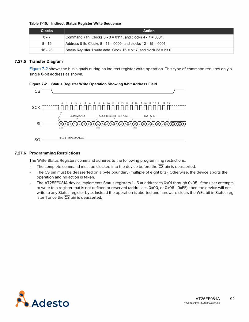
92AT25FF081A DS-AT25FF081A–183D–2021-01
7.27.5 Transfer Diagram
Figure 7-2 shows the bus signals during an indirect register write operation. This type of command requires only a single 8-bit address as shown.
Figure 7-2. Status Register Write Operation Showing 8-bit Address Field
7.27.6 Programming Restrictions
The Write Status Registers command adheres to the following programming restrictions.• The complete command must be clocked into the device before the CS pin is deasserted.• The CS pin must be deasserted on a byte boundary (multiple of eight bits). Otherwise, the device aborts the
operation and no action is taken.• The AT25FF081A device implements Status registers 1 - 5 at addresses 0x01 through 0x05. If the user attempts
to write to a register that is not defined or reserved (addresses 0x00, or 0x06 - 0xFF), then the device will not write to any Status register byte. Instead the operation is aborted and hardware clears the WEL bit in Status reg-ister 1 once the CS pin is deasserted.
Table 7-15. Indirect Status Register Write Sequence
Clocks Action0 - 7 Command 71h. Clocks 0 - 3 = 0111, and clocks 4 - 7 = 0001.
8 - 15 Address 01h. Clocks 8 - 11 = 0000, and clocks 12 - 15 = 0001.
16 - 23 Status Register 1 write data. Clock 16 = bit 7, and clock 23 = bit 0.
SCK
CS
SI
SO
MSB MSB
2 310 6 754 10 1198 12
HIGH-IMPEDANCE
A A A A A A AAMSB
D D D D D D D D
DATA IN
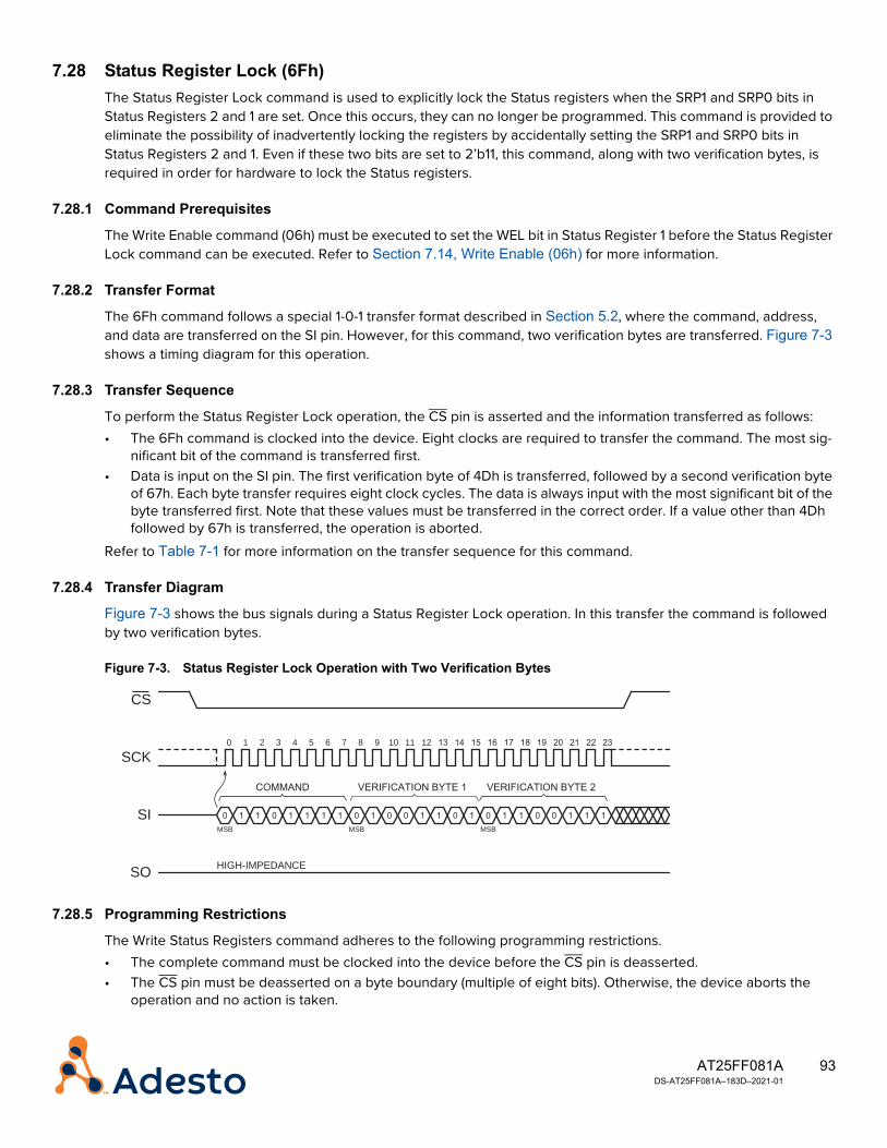
93AT25FF081A DS-AT25FF081A–183D–2021-01
7.28 Status Register Lock (6Fh)The Status Register Lock command is used to explicitly lock the Status registers when the SRP1 and SRP0 bits in Status Registers 2 and 1 are set. Once this occurs, they can no longer be programmed. This command is provided to eliminate the possibility of inadvertently locking the registers by accidentally setting the SRP1 and SRP0 bits in Status Registers 2 and 1. Even if these two bits are set to 2’b11, this command, along with two verification bytes, is required in order for hardware to lock the Status registers.
7.28.1 Command Prerequisites
The Write Enable command (06h) must be executed to set the WEL bit in Status Register 1 before the Status Register Lock command can be executed. Refer to Section 7.14, Write Enable (06h) for more information.
7.28.2 Transfer Format
The 6Fh command follows a special 1-0-1 transfer format described in Section 5.2, where the command, address, and data are transferred on the SI pin. However, for this command, two verification bytes are transferred. Figure 7-3 shows a timing diagram for this operation.
7.28.3 Transfer Sequence
To perform the Status Register Lock operation, the CS pin is asserted and the information transferred as follows:• The 6Fh command is clocked into the device. Eight clocks are required to transfer the command. The most sig-
nificant bit of the command is transferred first.• Data is input on the SI pin. The first verification byte of 4Dh is transferred, followed by a second verification byte
of 67h. Each byte transfer requires eight clock cycles. The data is always input with the most significant bit of the byte transferred first. Note that these values must be transferred in the correct order. If a value other than 4Dh followed by 67h is transferred, the operation is aborted.
Refer to Table 7-1 for more information on the transfer sequence for this command.
7.28.4 Transfer Diagram
Figure 7-3 shows the bus signals during a Status Register Lock operation. In this transfer the command is followed by two verification bytes.
Figure 7-3. Status Register Lock Operation with Two Verification Bytes
7.28.5 Programming Restrictions
The Write Status Registers command adheres to the following programming restrictions.• The complete command must be clocked into the device before the CS pin is deasserted.• The CS pin must be deasserted on a byte boundary (multiple of eight bits). Otherwise, the device aborts the
operation and no action is taken.
SCK
CS
SI
SO
MSB MSB
2 310 6 754 10 1198 12
HIGH-IMPEDANCE
MSB

94AT25FF081A DS-AT25FF081A–183D–2021-01
7.29 Deep Power Down (B9h)The Deep Power-Down command is used in conjunction with bit 7 (PDM) in Status register 4 to place the device into Deep Power-Down mode. When the PDM bit is set and the B9h command is executed, the device enters Deep Power Down mode.
When the device is in Deep Power-Down mode, most commands, including the Read Status Register command, are ignored. The only commands that are accepted while in this mode are the Resume from Deep Power-Down command (ABh), the Enable Reset command (66h), and the Reset Device (99h) commands. Since all other commands are ignored, the mode can be used as an extra protection mechanism against program and erase operations. When the CS pin is deasserted, the device enters the Deep Power-Down mode within the maximum time of tEDPD.
7.29.1 Command Prerequisites
None.
7.29.2 Transfer Format
The B9h command follows the 1-0-0 transfer format described in Section 5.2, where the command is transferred on the SI pin. No address or data are transferred for this command. Refer to Figure 5-1 for a timing diagram of this operation.
7.29.3 Transfer Sequence
To perform the Deep Power Down operation, the CS pin is asserted and the information transferred as follows:• The B9h command is clocked into the device. Eight clocks are required to transfer the command. The most sig-
nificant bit of the command is transferred first.• When the CS pin is deasserted, the device begins the power down operation. Refer to Table 7-1 for more information on the transfer sequence for this command.
7.29.4 Programming Restrictions
The Deep Power Down command adheres to the following programming restrictions.• The CS pin must be deasserted on a byte boundary (multiple of eight bits). Otherwise, the device aborts the
operation.• The B9h command is ignored if an internally self-timed operation such as a program or erase cycle is in prog-
ress. In this case, the B9h command must be reissued after the internally self-timed operation has been com-pleted. Software can monitor the RDY/BSY bit in Status Register 1 to determine when the program or erase operation has completed.

95AT25FF081A DS-AT25FF081A–183D–2021-01
7.30 Resume from Ultra-Deep Power Down / Deep Power Down with Device ID (ABh)In order to exit the Deep Power Down (DPD) mode and resume normal device operation, the Resume from Deep Power-Down (ABh) command must be issued. This command, along with the 66h/99h Reset Enable/Reset command, are the only commands that the device recognizes while in the Deep Power-Down mode. This command allows both the exit from DPD mode, as well as a fetch of the Device ID. Which operation is executed depends on the way in which CS is used as described below.
The ABh command can also be used to exit from Ultra-Deep Power Down (UDPD) mode. Execution of this command while in Ultra-Deep Power Down causes the device to initialize, and then enters standby mode, where it is ready to accept commands.
7.30.1 Command Options
As mentioned above, the ABh command can be used to exit both DPD and UDPD modes. In DPD mode, execution of the ABh command causes the device to exit the DPD state, and also fetch the device ID as described in Section 7.30.4 below. In UDPD mode, the ABh command is used to exit the UDPD state as described in Section 7.30.5 below. Table 7-16 shows how to exit the DPD and UDPD modes.
7.30.2 Command Prerequisites
None.
7.30.3 Transfer Format — Resume from Deep Power Down
For this operation, the ABh command follows the 1-0-0 transfer format described in Section 5.2, where the command is transferred on the SI pin. No address or data are transferred for this command. Refer to Figure 5-1 for a timing diagram of this operation.
7.30.4 Transfer Format — Resume from Deep Power Down and Obtain Device ID
For this operation, the ABh command follows the 1-1-1 transfer format described in Section 5.2, where the command is transferred on the SI pin and address and data on the SO pin. Refer to Figure 5-5 for a timing diagram of this operation. Note that no address is transferred for this command. Rather, three dummy bytes are transferred in place of the address.
7.30.5 Transfer Sequence — Resume from Deep Power Down
To perform the Resume from Deep Power Down operation, the CS pin is asserted and the information transferred as follows:• The ABh command is clocked into the device. Eight clocks are required to transfer the command. The most sig-
nificant bit of the command is transferred first.• For this operation, the CS pin must be deasserted on the 8th clock, immediately after the command is issued.
This causes the device begins the resume from power down operation. When the CS pin is deasserted after the 8th clock, the device exits the Deep Power-Down mode within the maximum time of tRDPD and returns to the standby mode. After the device has returned to the standby mode, normal command operations such as Read Array can be resumed.
Table 7-16. Options for Exiting DPD and UDPD Modes
CommandCurrently in DPD Mode?
Currently in UDPD Mode? Exit DPD Mode Exit UDPD Mode Fetch Device ID
ABh
No No No No Yes
Yes No Yes No Yes
No Yes No Yes No
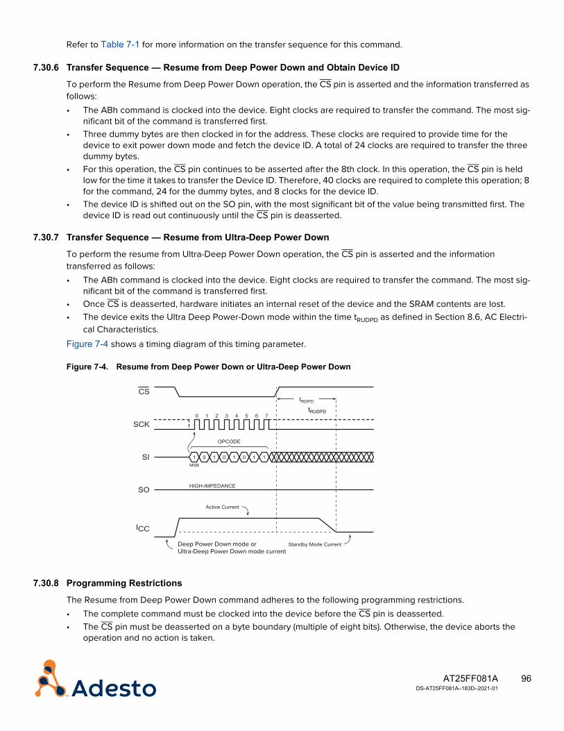
96AT25FF081A DS-AT25FF081A–183D–2021-01
Refer to Table 7-1 for more information on the transfer sequence for this command.
7.30.6 Transfer Sequence — Resume from Deep Power Down and Obtain Device ID
To perform the Resume from Deep Power Down operation, the CS pin is asserted and the information transferred as follows:• The ABh command is clocked into the device. Eight clocks are required to transfer the command. The most sig-
nificant bit of the command is transferred first.• Three dummy bytes are then clocked in for the address. These clocks are required to provide time for the
device to exit power down mode and fetch the device ID. A total of 24 clocks are required to transfer the three dummy bytes.
• For this operation, the CS pin continues to be asserted after the 8th clock. In this operation, the CS pin is held low for the time it takes to transfer the Device ID. Therefore, 40 clocks are required to complete this operation; 8 for the command, 24 for the dummy bytes, and 8 clocks for the device ID.
• The device ID is shifted out on the SO pin, with the most significant bit of the value being transmitted first. The device ID is read out continuously until the CS pin is deasserted.
7.30.7 Transfer Sequence — Resume from Ultra-Deep Power Down
To perform the resume from Ultra-Deep Power Down operation, the CS pin is asserted and the information transferred as follows:• The ABh command is clocked into the device. Eight clocks are required to transfer the command. The most sig-
nificant bit of the command is transferred first.• Once CS is deasserted, hardware initiates an internal reset of the device and the SRAM contents are lost.• The device exits the Ultra Deep Power-Down mode within the time tRUDPD as defined in Section 8.6, AC Electri-
cal Characteristics. Figure 7-4 shows a timing diagram of this timing parameter.
Figure 7-4. Resume from Deep Power Down or Ultra-Deep Power Down
7.30.8 Programming Restrictions
The Resume from Deep Power Down command adheres to the following programming restrictions.• The complete command must be clocked into the device before the CS pin is deasserted.• The CS pin must be deasserted on a byte boundary (multiple of eight bits). Otherwise, the device aborts the
operation and no action is taken.
SCK
CS
SI
SO
MSB
ICC
2 310
1 0 1 0 1 0 1 1
6 754
OPCODE
HIGH-IMPEDANCE
Deep Power-Down Mode Current
Active Current
Standby Mode Current
tRDPD
tRUDPD
Deep Power Down mode orUltra-Deep Power Down mode current
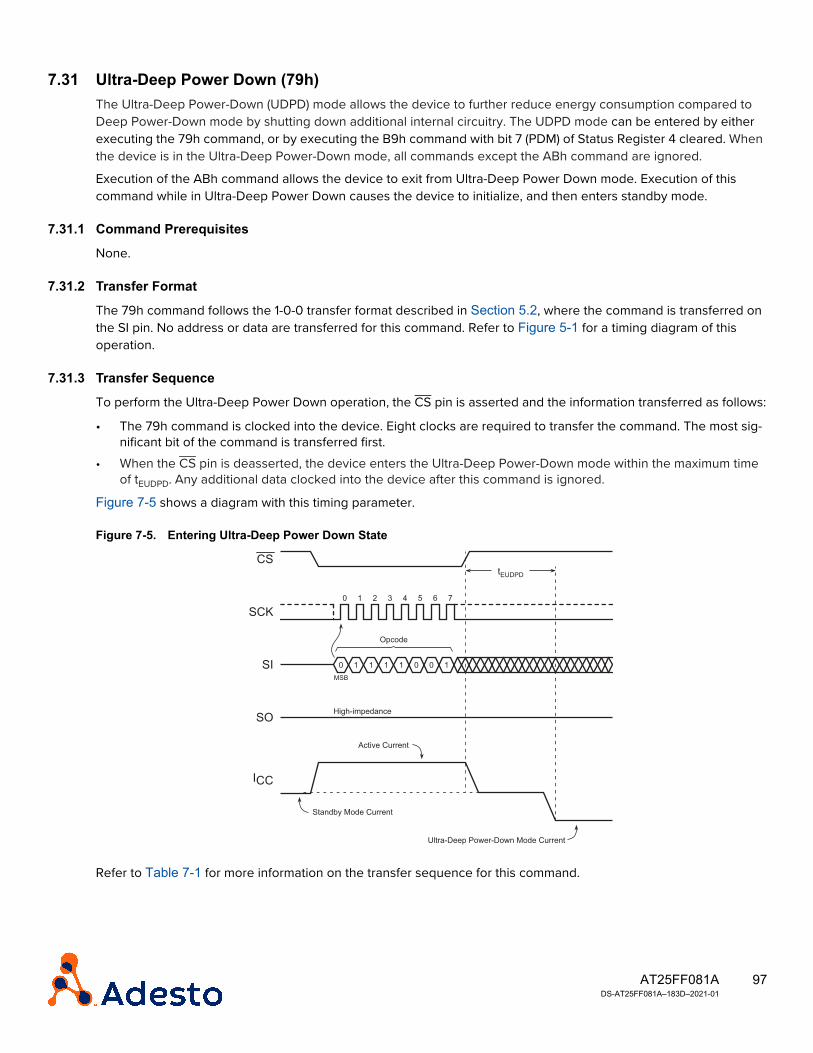
97AT25FF081A DS-AT25FF081A–183D–2021-01
7.31 Ultra-Deep Power Down (79h)The Ultra-Deep Power-Down (UDPD) mode allows the device to further reduce energy consumption compared to Deep Power-Down mode by shutting down additional internal circuitry. The UDPD mode can be entered by either executing the 79h command, or by executing the B9h command with bit 7 (PDM) of Status Register 4 cleared. When the device is in the Ultra-Deep Power-Down mode, all commands except the ABh command are ignored.
Execution of the ABh command allows the device to exit from Ultra-Deep Power Down mode. Execution of this command while in Ultra-Deep Power Down causes the device to initialize, and then enters standby mode.
7.31.1 Command Prerequisites
None.
7.31.2 Transfer Format
The 79h command follows the 1-0-0 transfer format described in Section 5.2, where the command is transferred on the SI pin. No address or data are transferred for this command. Refer to Figure 5-1 for a timing diagram of this operation.
7.31.3 Transfer Sequence
To perform the Ultra-Deep Power Down operation, the CS pin is asserted and the information transferred as follows:
• The 79h command is clocked into the device. Eight clocks are required to transfer the command. The most sig-nificant bit of the command is transferred first.
• When the CS pin is deasserted, the device enters the Ultra-Deep Power-Down mode within the maximum time of tEUDPD. Any additional data clocked into the device after this command is ignored.
Figure 7-5 shows a diagram with this timing parameter.
Figure 7-5. Entering Ultra-Deep Power Down State
Refer to Table 7-1 for more information on the transfer sequence for this command.
SCK
CS
SI
SO
MSB
ICC
2 310
0
6 754
Opcode
High-impedance
Ultra-Deep Power-Down Mode Current
Active Current
Standby Mode Current
tEUDPD
1 1 1 1 0 0 1

98AT25FF081A DS-AT25FF081A–183D–2021-01
7.31.4 Programming Restrictions
The following events can cause the Ultra-Deep Power Down operation to be aborted. • The CS pin must be deasserted on a byte boundary (multiple of eight bits). Otherwise, the device aborts the
operation and return to the standby mode once the CS pin is deasserted. In addition, the device defaults to the standby mode after a power cycle.
• The 79h command is ignored if an internally self-timed operation such as a program or erase cycle is in prog-ress. The 79h command must be reissued after the internally self-timed operation has been completed. Soft-ware can monitor the RDY/BSY bit in Status Register 1 to determine when the program or erase operation has completed.
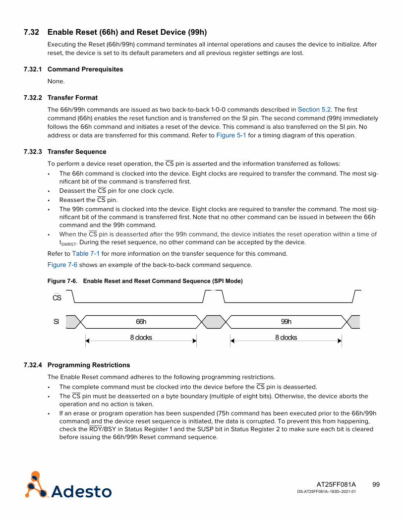
99AT25FF081A DS-AT25FF081A–183D–2021-01
7.32 Enable Reset (66h) and Reset Device (99h)Executing the Reset (66h/99h) command terminates all internal operations and causes the device to initialize. After reset, the device is set to its default parameters and all previous register settings are lost.
7.32.1 Command Prerequisites
None.
7.32.2 Transfer Format
The 66h/99h commands are issued as two back-to-back 1-0-0 commands described in Section 5.2. The first command (66h) enables the reset function and is transferred on the SI pin. The second command (99h) immediately follows the 66h command and initiates a reset of the device. This command is also transferred on the SI pin. No address or data are transferred for this command. Refer to Figure 5-1 for a timing diagram of this operation.
7.32.3 Transfer Sequence
To perform a device reset operation, the CS pin is asserted and the information transferred as follows:• The 66h command is clocked into the device. Eight clocks are required to transfer the command. The most sig-
nificant bit of the command is transferred first.• Deassert the CS pin for one clock cycle.• Reassert the CS pin.• The 99h command is clocked into the device. Eight clocks are required to transfer the command. The most sig-
nificant bit of the command is transferred first. Note that no other command can be issued in between the 66h command and the 99h command.
• When the CS pin is deasserted after the 99h command, the device initiates the reset operation within a time of tSWRST. During the reset sequence, no other command can be accepted by the device.
Refer to Table 7-1 for more information on the transfer sequence for this command.
Figure 7-6 shows an example of the back-to-back command sequence.
Figure 7-6. Enable Reset and Reset Command Sequence (SPI Mode)
7.32.4 Programming Restrictions
The Enable Reset command adheres to the following programming restrictions.• The complete command must be clocked into the device before the CS pin is deasserted.• The CS pin must be deasserted on a byte boundary (multiple of eight bits). Otherwise, the device aborts the
operation and no action is taken.• If an erase or program operation has been suspended (75h command has been executed prior to the 66h/99h
command) and the device reset sequence is initiated, the data is corrupted. To prevent this from happening, check the RDY/BSY in Status Register 1 and the SUSP bit in Status Register 2 to make sure each bit is cleared before issuing the 66h/99h Reset command sequence.
CS
66h 99hSI
8 clocks 8 clocks
100AT25FF081A DS-AT25FF081A–183D–2021-01
7.33 Terminate (F0h)In some applications, it may be necessary to prematurely terminate a program or erase operation rather than wait for the program or erase operation to complete normally. The Terminate command immediately aborts any operation in progress and returns the device to an idle state.
Since the need to terminate the operation is immediate, the Write Enable command does not need to be issued prior to the Terminate command. Therefore, the Terminate command operates independently of the state of the WEL bit in Status Register 1.
Once this command is issued, the operation in progress cannot be continued. To suspend and then continue an operation, use the Program/Erase Suspend (75h) and Program/Erase Resume (7Ah) commands.
7.33.1 Command Prerequisites
The Terminate command can be executed only if the command has been enabled by setting the Reset Enabled (RSTE) bit in Status Register 5 using the Write Status Register 5 command (71h + 05h address offset). This command must be executed before the Terminate command is executed. If the Reset command has not been enabled (the RSTE bit in is cleared), then any attempt at executing the Terminate command is ignored.
7.33.2 Transfer Format
The F0h command follows the 1-0-1 transfer format described in Section 5.2, where the command and data are transferred on the SI pin. Immediately after the command is transferred, a confirmation data byte is transferred. This byte is required by the hardware before the Terminate command can be executed. A timing diagram of this operation is shown in Figure 5-4.
7.33.3 Transfer Sequence
To perform device reset operation, the CS pin is asserted and the information transferred as follows:• The F0h command is clocked into the device. Eight clocks are required to transfer the command. The most sig-
nificant bit of the command is transferred first.• The D0h confirmation byte is clocked into the device. Eight clocks are required to transfer the command. The
most significant bit of the command is transferred first. Note that is the confirmation byte is any value other than D0h, the entire command is ignored and the device returns to the idle state.
• When the CS pin is deasserted after the D0h confirmation byte, the device initiates the terminate operation within a time of tSWTERM. During the terminate sequence, no other command can be accepted by the device.
Refer to Table 7-1 for more information on the transfer sequence for this command.
7.33.4 Programming Restrictions
The F0h Terminate command adheres to the following programming restrictions.• If a program or erase operation is in progress and cannot complete before the operation is terminated via the
F0h command, the contents of the page being programmed or erased cannot be guaranteed to be valid.• The F0h command does not reset the device configuration registers in volatile mode. If a reset of the internal
state is desired, perform a 66h/99h command. This command resets the device and all programmable parame-ters and all volatile register contents are lost.
• The CS pin must be deasserted on a byte boundary (multiple of eight bits). Otherwise, the device aborts the operation and returns to the standby mode once the CS pin is deasserted. In addition, the device defaults to the standby mode after a power cycle.
101AT25FF081A DS-AT25FF081A–183D–2021-01
7.34 Read Manufacturer/Device ID (90h)The Read Manufacturer/Device ID (90h) command provides both the JEDEC assigned manufacturer ID, and the specific device ID.
7.34.1 Command Prerequisites
None.
7.34.2 Transfer Format
The 90h command follows the 1-1-1 transfer format described in Section 5.2, where the command and address are transferred on the SI pin, and data is transferred on the SO pin. Refer to Figure 5-5 for timing diagram of this operation.
7.34.3 Transfer Sequence
To perform the Read Array operation, the CS pin is asserted and the information transferred as follows:• The 90h command is clocked into the device. Eight clocks are required to transfer the command. The most sig-
nificant bit of the command is transferred first.• Three dummy bytes are clocked in during the address phase. A total of 24 clocks are required. These three
dummy bytes are not used • Data is output on the SO pin. Two bytes are transferred, requiring a total of 16 clock cycles. The data is driven
onto the bus as follows:- 1st data clock: bit 7 of the manufacturer ID is output on the SO pin- 2nd data clock: bit 6 of the manufacturer ID is output on the SO pin- .........- 8th data clock: bit 0 of the manufacturer ID is output on the SO pin- 9th data clock: bit 7 of the device ID is output on the SO pin- 10th data clock: bit 6 of the device ID is output on the SO pin- .........- 16th data clock: bit 0 of the device ID is output on the SO pin
• Deasserting the CS pin terminates the read operation and puts the SO pin into high-impedance state. If the CS pin remains asserted, the device continues to shift out the manufacturer ID followed by the device ID.
Refer to Table 7-1 for more information on the transfer sequence for this command.
7.34.4 Programming Restrictions
None.
102AT25FF081A DS-AT25FF081A–183D–2021-01
7.35 Quad I/O Read Manufacturer/Device ID (94h)The Read Manufacturer/Device ID command operates in quad I/O mode, where the SI, SO, WP, and HOLD pins are all bidirectional, to allow the manufacturer and device ID information to be transmitted at four times the speed of the Read Manufacturer/Device ID command (90h).
7.35.1 Command Prerequisites
None.
7.35.2 Transfer Format
The 94h command follows the 1-4-4 transfer format described in Section 5.6, where the command is transferred on the SI pin, and the address and data are transferred on the SI, SO, WP, and HOLD pins. Refer to Figure 5-13 for a timing diagram of this transaction.
7.35.3 Transfer Sequence
To perform the Quad Read Manufacturer/Device ID command, the CS pin is asserted and the information transferred as follows:• The 94h command is clocked into the device. Eight clocks are required to transfer the command. The most sig-
nificant bit of the command is transferred first.• Three dummy address bytes are clocked in during the address phase. A total of 6 clocks are required. These
three dummy bytes are ignored.• The mode byte is clocked into the device. Two clocks are required to transfer the command. The one dummy
byte is ignored.• Four dummy clocks are driven to the device prior to the output of data.• Data is output on the SI, SO, WP, and HOLD pins. Each byte transfer requires two clock cycles. The data is always
output with the most significant bit of the byte transferred first. The first byte transferred is the manufacturer ID. The second byte transferred is the device ID. As long as CS is asserted, hardware continues to shift these two bytes out onto the bus. Each data byte is shifted out of the device as follows: - First data clock: bit 7 of the manufacturer ID is output on the HOLD pin- First data clock: bit 6 of the manufacturer ID is output on the WP pin- First data clock: bit 5 of the manufacturer ID is output on the SO pin- First data clock: bit 4 of the manufacturer ID is output on the SI pin- Second data clock: bit 3 of the manufacturer ID is output on the HOLD pin- Second data clock: bit 2 of the manufacturer ID is output on the WP pin- Second data clock: bit 1 of the manufacturer ID is output on the SO pin- Second data clock: bit 0 of the manufacturer ID is output on the SI pin- In clocks 3 and 4, the device ID is shifted out on byte 2 in the same manner as above
7.35.4 Programming Restrictions
None.
103AT25FF081A DS-AT25FF081A–183D–2021-01
7.36 Read JEDEC ID (9Fh)The Read JEDEC ID command allows software to identify the manufacturer and device ID information for the device while it is in the system. This command allows the ID information to be read out a relatively low clock frequency to ensure the device can be identified. Once the identification process is complete, the application can increase the clock frequency as necessary. For more information, refer to the Serial Flash Discoverable Parameters (SFDP) JEDEC specification, edition JESD216C.
7.36.1 Command Prerequisites
None.
7.36.2 Transfer Format
The 9Fh command follows the 1-0-1 transfer format described in Section 5.2, where the command is transferred on the SI pin, and data is transferred on the SO pin. Refer to Figure 7-7 for timing diagram of this operation. Note that no address is required for this type of read operation.
7.36.3 Transfer Sequence
To perform the JEDEC ID operation, the CS pin is asserted and the information transferred as follows:• The 9Fh command is clocked into the device. Eight clocks are required to transfer the command. The most sig-
nificant bit of the command is transferred first. No address is required for this transaction.• Data is output on the SO pin. Five bytes are transferred, requiring a total of 40 clock cycles. The data is driven
onto the bus as follows:- 1st data clock: bit 7 of the manufacturer ID is output on the SO pin- .........- 8th data clock: bit 0 of the manufacturer ID is output on the SO pin- 9th data clock: bit 7 of the device ID byte 1 is output on the SO pin- .........- 16th data clock: bit 0 of the device ID byte 1 is output on the SO pin- 17th data clock: bit 7 of the device ID byte 2 is output on the SO pin- .........- 24th data clock: bit 0 of the device ID byte 2 is output on the SO pin- 25th data clock: bit 7 of the extended device string length byte is output on the SO pin- .........- 32nd data clock: bit 0 of the extended device string length byte is output on the SO pin- 33rd data clock: bit 7 of the extended device string value byte is output on the SO pin- .........- 40th data clock: bit 0 of the extended device string value byte is output on the SO pin
• Deasserting the CS pin terminates the read operation and puts the SO pin into high-impedance state. If the CS pin remains asserted, the device continues to shift out the manufacturer ID followed by the device ID.
Refer to Table 7-1 for more information on the transfer sequence for this command.
The following tables below show the exact contents of each data byte.
104AT25FF081A DS-AT25FF081A–183D–2021-01
7.36.4 Transfer Diagram
Figure 7-7 shows the bus signals during an indirect register read operation. This type of command requires only a single 8-bit address as shown.
Table 7-17. Manufacturer and Device ID Details
Data Type Bit 7 Bit 6 Bit 5 Bit 4 Bit 3 Bit 2 Bit 1 Bit 0Hex
Value Details
Manufacturer IDJEDEC Assigned Code
1Fh JEDEC Code: 0001 1111 (1Fh for Adesto)0 0 0 1 1 1 1 1
Device ID (Part 1)Family Code Density Code
45h Family Code: 010 (4h) Density Code: 00101 (05h)0 1 0 0 0 1 0 1
Device ID (Part 2)Sub Code Sub-family Code Revision Code
08hSub Code: 000 Sub-family Code: 01 Revision Code: 0000 0 0 0 1 0 0 0
Device ID (Part 3) (EDI String Length)
Number of Extended Device ID Bytes to Follow01h Bytes to follow: 1
0 0 0 0 0 0 0 1
Device ID (Part 4) (EDI String Value)
Extended device Identity Value0xh x: Device Variant/Option. See table below.
0 0 0 0 x x x x
Table 7-18. Device ID Part 4 Variants — EDI String Value
EDI String Value Variant
00h Initial device
01h TBD
02h TBD
03h TBD
04h TBD
05h TBD
06h TBD
07h TBD
08h - 0Fh Reserved

105AT25FF081A DS-AT25FF081A–183D–2021-01
Figure 7-7. Read JEDEC ID
7.36.5 Programming Restrictions
None.
SCK
CS
SI
SO
60
9Fh
87 46
OPCODE
1Fh 45h 02h 00h
MANUFACTURER ID DEVICE IDBYTE1
DEVICE IDBYTE2
EXTENDEDDEVICE
INFORMATIONSTRING LENGTH
HIGH-IMPEDANCE
14 1615 22 2423 30 3231
Note: Each transition shown for SI and SO represents one byte (8 bits)
0x
EXTENDEDDEVICE
INFORMATIONSTRING VALUE
38 4039
08h 01h

106AT25FF081A DS-AT25FF081A–183D–2021-01
7.37 Serial Flash Discoverable Parameters (5Ah)The device contains a 256-byte Serial Flash Discoverable Parameter (SFDP) register. The SFDP register can be sequentially read in a similar fashion to the Read Array operation up to the maximum clock frequency specified by fSCK.
7.37.1 Command Prerequisites
None.
7.37.2 Transfer Format
The 5Ah command follows the 1-1-1 transfer format described in Section 5.1.1, where the command, address, and dummy bytes are transferred on the SI pin, and data is transferred on the SO pin. Figure 5-6 shows a timing diagram of a read operation with dummy bytes. In this diagram one byte of data is transferred. Additional bytes can be transferred as long as the CS pin is asserted.
7.37.3 Transfer Sequence
To perform the SFDP operation, the CS pin is asserted and the information transferred as follows:• The 5Ah command is clocked into the device. Eight clocks are required to transfer the command. The most sig-
nificant bit of the command is transferred first.• Three address bytes are clocked in to specify the starting address location of the first byte to read within the
memory array. A total of 24 clocks are required to transfer the address. The most significant bit of the address (A[23]) is transferred first.
• Following the three address bytes, an additional dummy byte must be clocked into the device.• Data is output on the SO pin. Each byte transfer requires eight clock cycles. The data is always output with the
most significant bit of the byte transferred first. The number of bytes transferred is determined by software. The transfer can be anywhere from a single byte to the entire SFDP value. The most significant bit of each data byte is transferred first.
• Deasserting the CS pin terminates the read operation and puts the SO pin into high-impedance state. The CS pin can be deasserted at any time and does not require a full byte of data be read. The format of the SFDP re ister follows the format provided in JEDEC Standard No. 216 Rev B.
7.37.4 Programming Restrictions
When the last byte (0000FFh) of the SFDP Security Register has been read, the device continues reading back at the beginning of the register (000000h). No delays are incurred when wrapping around from the end of the register to the beginning of the register.
7.37.5 SFDP Organization
Contact Adesto for SFDP table information.
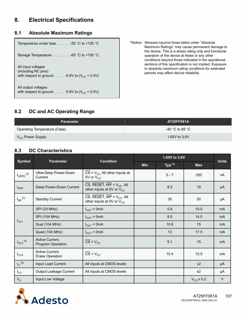
107AT25FF081A DS-AT25FF081A–183D–2021-01
8. Electrical Specifications
8.1 Absolute Maximum Ratings
8.2 DC and AC Operating Range
Temperature under bias . . . . . . . -55 °C to +125 °C *Notice: Stresses beyond those listed under “Absolute Maximum Ratings” may cause permanent damage to the device. This is a stress rating only and functional operation of the device at these or any other conditions beyond those indicated in the operational sections of this specification is not implied. Exposure to absolute maximum rating conditions for extended periods may affect device reliability.
Storage Temperature . . . . . . . . . -65 °C to +150 °C
All input voltages (including NC pins) with respect to ground . . . . . -0.6V to (VCC + 0.5V)
All output voltages with respect to ground . . . . . -0.6V to (VCC + 0.5V)
Parameter AT25FF081A
Operating Temperature (Case) -40 °C to 85 °C
VCC Power Supply 1.65V to 3.6V
8.3 DC Characteristics
Symbol Parameter Condition1.65V to 3.6V
UnitsMin Typ (1) Max
IUDPD (2) Ultra-Deep Power-Down
CurrentCS = VCC. All other inputs at 0V or VCC
5 - 7 250 nA
IDPD Deep Power-Down Current CS, RESET, WP = VCC. All other inputs at 0V or VCC
8.5 19 µA
ISB (3)
Standby Current CS, RESET, WP = VCC. All other inputs at 0V or VCC
30 50 µA
ICC1
SPI (33 MHz) IOUT = 0mA 5.6 10.5 mA
SPI (104 MHz) IOUT = 0mA 8.5 14.5 mA
Dual (104 MHz) IOUT = 0mA 10.6 15 mA
Quad (104 MHz) IOUT = 0mA 13 17.5 mA
ICC3 (4) Active Current,
Program Operation CS = VCC 9.1 15 mA
ICC4Active Current, Erase Operation CS = VCC 10.4 15.5 mA
ILI (5) Input Load Current All inputs at CMOS levels ±2 µA
ILO Output Leakage Current All inputs at CMOS levels ±2 µA
VIL Input Low Voltage VCC x 0.2 V

108AT25FF081A DS-AT25FF081A–183D–2021-01
VIH Input High Voltage VCC x 0.8 V
VOL Output Low Voltage IOL = 100 µA 0.2 V
VOH Output High Voltage IOH = -100 µA VCC - 0.2 V
1. Typical values measured at 1.8V @ 25 oC for the 1.65V to 3.6V range.
2. IUDPD value is estimated. Not 100% tested.
3. During continuous read mode (0-4-4), ISB may exceed maximum limit.
4. Checkerboard pattern.
5. WP (IO2) and HOLD/RESET (IO3) pins have an internal pull-up resistor. It's input load current is +2 / -30 μA.
8.4 AC Characteristics - Maximum Clock Frequencies
Symbol Parameter1.65V to 3.6V 2.7V to 3.6V
UnitsMin Typ Max (1)
1. See Tables 7.2 and 7.3 for the maximum frequency of EBh/E7h commands in various modes.
Min Typ Max
fSCK
Maximum clock frequency for all operations (except 03h, 0Bh, 3Bh, 6Bh, EBh, and E7h commands)
108 133 MHz
Maximum clock frequency for 0Bh and 3Bh commands 108 108 MHz
Maximum clock frequency for 6Bh command 100 108 MHz
Maximum clock frequency for EBh and E7h commands 108 133 MHz
fRDLFMaximum clock frequency for 03h command (Read Array – Low Frequency) 50 50 MHz
8.5 AC Characteristics – All Other Parameters
Symbol (1) Parameter1.65V to 3.6V
UnitsMin Typ Max
tCLKH SCK High Time 4.5 ns
tCLKL SCK Low Time 4.5 ns
tCLKR Clock Rise Time, Peak-to-Peak (Slew Rate) 0.75 V/ns
tCLKF Clock Fall Time, Peak-to-Peak (Slew Rate) 0.75 V/ns
tCSH Minimum CS High Time 35 ns
tCSLS CS Low Setup Time (relative to clock) 6 ns
8.3 DC Characteristics (continued)
Symbol Parameter Condition1.65V to 3.6V
UnitsMin Typ (1) Max
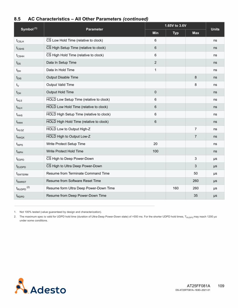
109AT25FF081A DS-AT25FF081A–183D–2021-01
tCSLH CS Low Hold Time (relative to clock) 6 ns
tCSHS CS High Setup Time (relative to clock) 6 ns
tCSHH CS High Hold Time (relative to clock) 6 ns
tDS Data In Setup Time 2 ns
tDH Data In Hold Time 1 ns
tDIS Output Disable Time 8 ns
tV Output Valid Time 8 ns
tOH Output Hold Time 0 ns
tHLS HOLD Low Setup Time (relative to clock) 6 ns
tHLH HOLD Low Hold Time (relative to clock) 6 ns
tHHS HOLD High Setup Time (relative to clock) 6 ns
tHHH HOLD High Hold Time (relative to clock) 6 ns
tHLQZ HOLD Low to Output High-Z 7 ns
tHHQX HOLD High to Output Low-Z 7 ns
tWPS Write Protect Setup Time 20 ns
tWPH Write Protect Hold Time 100 ns
tEDPD CS High to Deep Power-Down 3 µs
tEUDPD CS High to Ultra Deep Power-Down 3 µs
tSWTERM Resume from Terminate Command Time 50 µs
tSWRST Resume from Software Reset Time 260 µs
tRUDPD (2) Resume form Ultra Deep Power-Down Time 160 260 µs
tRDPD Resume from Deep Power-Down Time 35 µs
1. Not 100% tested (value guaranteed by design and characterization).
2. The maximum spec is valid for UDPD hold time (duration of Ultra-Deep Power-Down state) of >550 ms. For the shorter UDPD hold times, TRUDPD may reach 1200 μs under some conditions.
8.5 AC Characteristics – All Other Parameters (continued)
Symbol (1) Parameter1.65V to 3.6V
UnitsMin Typ Max

110AT25FF081A DS-AT25FF081A–183D–2021-01
8.6 Program and Erase Characteristics
Symbol Parameter1.65V - 3.6V 2.7V - 3.6V
UnitsMin Typ (1)
1. Typical values measured at 1.8V at 25 oC for 1.65V - 3.6V, and at 3.3V at 25 oC for 2.7V - 3.6V.
Max (2)
2. Unless otherwise specified, maximum is worst case measurement at cycling conditions after 100K cycles.
Min Typ(1) Max(2)
tPP Page Program Time (256 Bytes) 3.6 6.5 3.0 6.5 ms
tBP (3)
3. Program time after the first byte varies.
Byte Program Time 32 32 µs
tBLKE Block Erase Time
4 kB 70 180 60 180 ms
32 kB 500 1200 450 1200 ms
64 kB 1000 2400 900 2400 ms
tCHPE Chip Erase Time (8M density) 16 15 sec
tSUS
Suspend Time (Program) 50 50 µs
Suspend Time (Erase) 50 50 µs
tRES
Resume Time (Program) 8 10 8 10 µs
Resume Time (Erase) 8 10 8 10 µs
tOTPPOTP Security Register Program Time (<= 10K) 5 6 5 6 ms
tWRSR Write Status Register Time 13 37 13 37 ms
111AT25FF081A DS-AT25FF081A–183D–2021-01
8.7 Power On TimingWhen power is first applied to the device, or when recovering from a reset condition, the output pin (SO) will be in a high impedance state, and a high-to-low transition on the CS pin is required to start a valid instruction. The SPI mode (Mode 3 or Mode 0) is automatically selected on every falling edge of CS by sampling the inactive clock state.
As the device initializes, there will be a transient current demand. The system needs to be capable of providing this current to ensure correct initialization. During power-up, the device must not be accessed for at least the minimum tVCSL time after the supply voltage reaches the minimum VCC level (VCC min). While the device is being powered-up, the internal Power-On Reset (POR) circuitry keeps the device in a reset mode until the supply voltage rises above the minimum VCC. During this time, all operations are disabled and the device will not respond to any commands. (the tVCSL time is measured from when VCC reaches VCC min.)
If Power On Reset (POR) has not been properly completed by the end of tVCSL, the execution of a JEDEC Reset sequence restarts the POR process. This ensures the device can complete POR sequence, even if some aspect of system Power-On voltage ramp-up causes the POR to not initiate or complete correctly.
Figure 8-8 shows the AC timing during power-up.
Figure 8-8. AC Timing During Device Power Up
1. 30000 µs/V at -15 oC to 85 oC.
Table 8-19. Power On Timing Requirements
Symbol Parameter1.65V - 3.6V
UnitsMin Typ Max
tVCSL Minimum VCC to full operation permitted 260 µs
tVR VCC rise time (from 0V to VCCmin) 1 6000 1 µs/V
tPWD VCC brown-out low time 300 µs
VPWDMAX Maximum VCC brown-out 0.2 V
Vcc
tVCSL Full Operation Permitted
tVR
VCCmin
0V

112AT25FF081A DS-AT25FF081A–183D–2021-01
Figure 8-9 shows the AC power-up timing after a brown-out condition.
Figure 8-9. AC Power-up Timing After a Brown-Out
8.8 AC Timing Diagrams
Figure 8-10. Serial Input Timing
Figure 8-11. Serial Output Timing
Full Operation Permitted
Vcc
tVCSL
tVRtPWD
VPWDMAX
VCCmin
CS
SI
SCK
SO
tV
tCLKH tCLKL tDIS
tV
tOH
SI/SO/WP/HOLD
113AT25FF081A DS-AT25FF081A–183D–2021-01
Figure 8-12. WP Timing for Write Status Register Command
Figure 8-13. HOLD Timing – Serial Input
Figure 8-14. HOLD Timing – Serial Output
WP
SI
SCK
SO
0 0 0
HIGH-IMPEDANCE
MSBX
tWPS tWPH
CS
LSB OFWRITE STATUS REGISTER
DATA BYTE
MSB OFWRITE STATUS REGISTER
OPCODE
MSB OFNEXT OPCODE
CS
SI
SCK
SO
tHHH tHLS
tHLH tHHS
HOLD
HIGH-IMPEDANCE
CS
SI
SCK
SO
tHHH tHLS
tHLQZ
tHLH tHHS
HOLD
tHHQX

114AT25FF081A DS-AT25FF081A–183D–2021-01
9. Ordering Information
Note: Contact Adesto for more information on die/wafer options
Table 9-1. Valid Ordering Code Table
Valid Part NumberAvailable to Order
Mechanical Drawing Description
Lead Finish
Operating Voltage
Temperature Range
AT25FF081A-SSHN-BAT25FF081A-SSHN-T Yes 8S1
8-lead, 0.150" Narrow Plastic Gull Wing Small Outline Package (JEDEC SOIC)
NiPdAu 1.65V to 3.6V
Industrial(-40°C to +85°C)
AT25FF081A-SHN-BAT25FF081A-SHN-T Yes 8S2
8-lead, 0.208” Wide Plastic Gull Wing Small Outline Package (EIAJ SOIC)
AT25FF081A-MAHN-T Yes 8MA3
8-pad, 2 x 3 x 0.6 mm, Thermally Enhanced Plastic Ultra Thin Dual Flat No Lead Package (UDFN)
NiPdAu 1.65V to 3.6V
Industrial(-40°C to +85°C)
AT25FF081A-UUN-T Yes 8-WLCSP 8-ball, 3 x 2 x 3 mm Ball Matrix, 0.35 mm Z-Height SnAgCu 1.65V to
3.6VIndustrial
(-40°C to +85°C)
AT25FF081A-DWF Contact Adesto
Contact Adesto Die in Wafer Form -- 1.65V to
3.6VIndustrial
(-40°C to +85°C)
AT 25FF 081 A - SS H N - B
Designator
Product Family
Device Density081 = 8 Mbit
Revision
ShippingB = BulkT = Tape
Operating VoltageN = 1.65V - 3.6V
Device GradeH = Green, NiPdAu finish
Industrial Temperature Range(-40 oC - +85 oC)
U = Green, MatteSn or Sn alloy
Package OptionsSS = 8-lead 0.150” narrow SOICS = 8-lead 0.208” wide SOICMA = 8-pad 2 x 3 x 0.6 mm UDFNU = 8-ball WLCSP

115AT25FF081A DS-AT25FF081A–183D–2021-01
10. Packaging InformationThe AT25FF081A device supports the following package types:
• 8S1, 8-lead 0.150 narrow body JEDEC SOIC
• 8S2, 8-lead 0.208 wide body EIAJ
• 8MA3, 2 x 3 x 0.6 mm UDFN
• 8-WLCSP, 8-ball 3 x 2 x 3 array WLCSP
Each of these packages is described in the following subsections.
116AT25FF081A DS-AT25FF081A–183D–2021-01
10.1 8S1 – JEDEC SOIC

117AT25FF081A DS-AT25FF081A–183D–2021-01
10.2 8S2 – 8-lead EIAJ SOIC

118AT25FF081A DS-AT25FF081A–183D–2021-01
10.3 8MA3 – 2 x 3 UDFN
119AT25FF081A DS-AT25FF081A–183D–2021-01
10.4 8-WLCSP — 8-ball 3 x 2 x 3 WLCSP
Revision8-ball (3 x 2 x 3 Array)Wafer Level Chip Scale Package (WLCSP)
TITLE
Package Drawing Contact:[email protected]
1767
1404
321
E
D
C
B
A
PIN A1 MARK3 2 1
E
D
C
B
A
800
165±17 250
SIDE VIEW
BOTTOM VIEWTOP VIEW
All dimensions in micrometers (μm)
210±31
25
440±21
400
BSL
Internal Package Identifier
Ordering Part Number Identifier
DEC UD A
350
700
200
200
400
PIN A1 MARK

120AT25FF081A DS-AT25FF081A–183D–2021-01
11. Revision History
Revision Date Change History
A 3/2020 Initial release of AT25FF081A 8 Mbit data sheet.
B 5/2020
Updated low power dissipation numbers in Features on page 1. Updated Table 8-3, DC Characteristics. Updated Table 8-4, Maximum Operating Frequencies Updated Table 8-5, AC Characteristics Updated Table 8-6, Program and Erase Characteristics Added 2.7V - 3.6V voltage option to Table 8-6. Updated Section 10.3, 8MA3 2 x 3 UDFN package drawing. Changed data sheet status from ADVANCED to PRELIMINARY.
C 8/2020
Updated Table 7-2, Frequency and Number of Dummy Clocks Based on Command Type. Added 2.7V - 3.6V voltage option to Table 8-4. Updated frequency information on page 1. Updated power dissipation information on page 1.
D 01/2021
Changed Table 8-19 to indicate temperature dependency. Updated Table 7-2 and added Table 7-3 in Section 7.4, XiP Mode Read Command. Updated Section 8.3, Maximum Clock Frequencies. Changed value in second footnote of Section 8.5, AC Characteristics - All Other Parameters. Deleted tPE row from table in Section 8.6, Program and Erase Characteristics. Removed footnote 4 from Section 8.3, DC Characteristics.

Corporate OfficeCalifornia | USAAdesto Headquarters3600 Peterson WaySanta Clara, CA 95054 Phone: (+1) 408.400.0578Email: [email protected]
Copyright © 2021 Adesto Technologies Corporation. All rights reserved. DS-AT25FF081A–183D–2021-01
Adesto and the Adesto logo are trademarks or registered trademarks of Adesto Technologies Corporation in the United States and other countries. Other company, product, and service names may be trademarks or service marks of others. Adesto products are covered by one or more patents listed at http://www.adestotech.com/patents.
Disclaimer: Adesto Technologies Corporation (“Adesto”) makes no warranties of any kind, other than those expressly set forth in Adesto’s Terms and Conditions of Sale at http://www.adestotech.com/terms-conditions. Adesto assumes no responsibility or obligations for any errors which may appear in this document, reserves the right to change devices or specifications herein at any time without notice, and does not make any commitment to update the information contained herein. No licenses to patents or other intellectual property of Adesto are granted by Adesto herewith or in connection with the sale of Adesto products, expressly or by implication. Adesto’s products are not authorized for use in medical applications (including, but not limited to, life support systems and other medical equipment), weapons, military use, avionics, satellites, nuclear applications, or other high risk applications (e.g., applications that, if they fail, can be reasonably expected to result in personal injury or death) or automotive applications, without the express prior written consent of Adesto.
Mouser Electronics
Authorized Distributor
Click to View Pricing, Inventory, Delivery & Lifecycle Information: Dialog Semiconductor:
AT25FF081A-MAHN-T AT25FF081A-SHN-B AT25FF081A-SHN-T AT25FF081A-SSHN-B AT25FF081A-SSHN-T
AT25FF081A-UUN-T