vs1011 datasheet - vlsi solution-home (mp3: cbr, vbr, abr); layers i & ii (mp1, mp2) optional;...
TRANSCRIPT
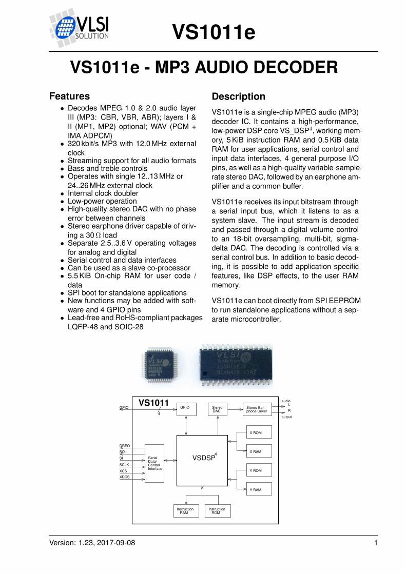
VS1011e
VS1011e - MP3 AUDIO DECODERFeatures
• Decodes MPEG 1.0 & 2.0 audio layerIII (MP3: CBR, VBR, ABR); layers I &II (MP1, MP2) optional; WAV (PCM +IMA ADPCM)
• 320 kbit/s MP3 with 12.0 MHz externalclock
• Streaming support for all audio formats• Bass and treble controls• Operates with single 12..13 MHz or
24..26 MHz external clock• Internal clock doubler• Low-power operation• High-quality stereo DAC with no phase
error between channels• Stereo earphone driver capable of driv-
ing a 30 Ω load• Separate 2.5..3.6 V operating voltages
for analog and digital• Serial control and data interfaces• Can be used as a slave co-processor• 5.5 KiB On-chip RAM for user code /
data• SPI boot for standalone applications• New functions may be added with soft-
ware and 4 GPIO pins• Lead-free and RoHS-compliant packages
LQFP-48 and SOIC-28
Instruction RAM
Instruction ROM
Stereo DAC
L
RStereo Ear−phone Driver
audio
output
X ROM
X RAM
Y ROM
Y RAM
VSDSP4
SerialData/ControlInterface
DREQ
SO
SI
SCLK
XCS
VS1011GPIO
4
GPIO
XDCS
DescriptionVS1011e is a single-chip MPEG audio (MP3)decoder IC. It contains a high-performance,low-power DSP core VS_DSP4, working mem-ory, 5 KiB instruction RAM and 0.5 KiB dataRAM for user applications, serial control andinput data interfaces, 4 general purpose I/Opins, as well as a high-quality variable-sample-rate stereo DAC, followed by an earphone am-plifier and a common buffer.
VS1011e receives its input bitstream througha serial input bus, which it listens to as asystem slave. The input stream is decodedand passed through a digital volume controlto an 18-bit oversampling, multi-bit, sigma-delta DAC. The decoding is controlled via aserial control bus. In addition to basic decod-ing, it is possible to add application specificfeatures, like DSP effects, to the user RAMmemory.
VS1011e can boot directly from SPI EEPROMto run standalone applications without a sep-arate microcontroller.
Version: 1.23, 2017-09-08 1
VS1011eCONTENTS
Contents
VS1011 1
Table of Contents 2
List of Figures 5
1 Licenses 6
2 Disclaimer 6
3 Definitions 6
4 Characteristics & Specifications 74.1 Absolute Maximum Ratings . . . . . . . . . . . . . . . . . . . . . . . . . . . . . 74.2 Recommended Operating Conditions . . . . . . . . . . . . . . . . . . . . . . . . 74.3 Analog Characteristics . . . . . . . . . . . . . . . . . . . . . . . . . . . . . . . . 84.4 Power Consumption . . . . . . . . . . . . . . . . . . . . . . . . . . . . . . . . . 84.5 Digital Characteristics . . . . . . . . . . . . . . . . . . . . . . . . . . . . . . . . . 94.6 Switching Characteristics - Boot Initialization . . . . . . . . . . . . . . . . . . . . 9
5 Packages and Pin Descriptions 105.1 Packages . . . . . . . . . . . . . . . . . . . . . . . . . . . . . . . . . . . . . . . 10
5.1.1 LQFP-48 . . . . . . . . . . . . . . . . . . . . . . . . . . . . . . . . . . 105.1.2 SOIC-28 . . . . . . . . . . . . . . . . . . . . . . . . . . . . . . . . . . 12
5.2 Pin Descriptions . . . . . . . . . . . . . . . . . . . . . . . . . . . . . . . . . . . . 135.2.1 LQFP-48 Pin Descriptions . . . . . . . . . . . . . . . . . . . . . . . . 135.2.2 SOIC-28 Pin Descriptions . . . . . . . . . . . . . . . . . . . . . . . . 14
6 Connection Diagram, LQFP-48 15
7 SPI Buses 167.1 General . . . . . . . . . . . . . . . . . . . . . . . . . . . . . . . . . . . . . . . . 167.2 SPI Bus Pin Descriptions . . . . . . . . . . . . . . . . . . . . . . . . . . . . . . . 16
7.2.1 VS10xx Native Modes (New Mode, recommended) . . . . . . . . . . 167.2.2 VS1001 Compatibility Mode (deprecated, do not use in new designs) 16
7.3 Serial Protocol for Serial Data Interface (SDI) . . . . . . . . . . . . . . . . . . . 177.3.1 General . . . . . . . . . . . . . . . . . . . . . . . . . . . . . . . . . . 177.3.2 SDI in VS10xx Native Modes (New Mode, recommended) . . . . . . 177.3.3 SDI in VS1001 Compatibility Mode . . . . . . . . . . . . . . . . . . . 18
7.4 Data Request Pin DREQ . . . . . . . . . . . . . . . . . . . . . . . . . . . . . . . 197.5 Serial Protocol for Serial Command Interface (SCI) . . . . . . . . . . . . . . . . 19
7.5.1 General . . . . . . . . . . . . . . . . . . . . . . . . . . . . . . . . . . 197.5.2 SCI Read . . . . . . . . . . . . . . . . . . . . . . . . . . . . . . . . . 207.5.3 SCI Write . . . . . . . . . . . . . . . . . . . . . . . . . . . . . . . . . 20
7.6 SPI Timing Diagram . . . . . . . . . . . . . . . . . . . . . . . . . . . . . . . . . 217.7 SPI Examples with SM_SDINEW and SM_SDISHARED set . . . . . . . . . . . 22
7.7.1 Two SCI Writes . . . . . . . . . . . . . . . . . . . . . . . . . . . . . . 227.7.2 Two SDI Bytes . . . . . . . . . . . . . . . . . . . . . . . . . . . . . . . 227.7.3 SCI Operation in Middle of Two SDI Bytes . . . . . . . . . . . . . . . 23
Version: 1.23, 2017-09-08 2
VS1011eCONTENTS
8 Functional Description 248.1 Main Features . . . . . . . . . . . . . . . . . . . . . . . . . . . . . . . . . . . . . 248.2 Supported Audio Codecs . . . . . . . . . . . . . . . . . . . . . . . . . . . . . . . 24
8.2.1 Supported MP1 (MPEG layer I) Formats . . . . . . . . . . . . . . . . 248.2.2 Supported MP2 (MPEG layer II) Formats . . . . . . . . . . . . . . . . 258.2.3 Supported MP3 (MPEG layer III) Formats . . . . . . . . . . . . . . . 258.2.4 Supported RIFF WAV Formats . . . . . . . . . . . . . . . . . . . . . . 26
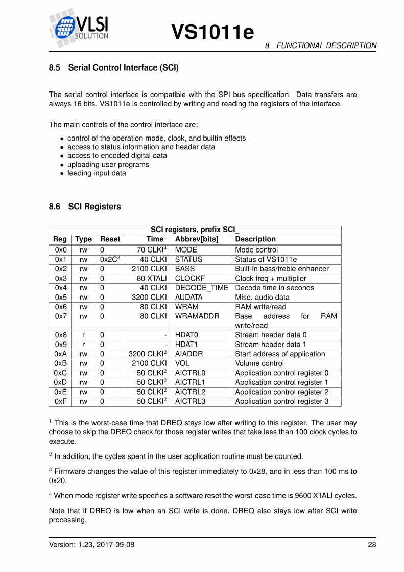
8.3 Data Flow of VS1011e . . . . . . . . . . . . . . . . . . . . . . . . . . . . . . . . 278.4 Serial Data Interface (SDI) . . . . . . . . . . . . . . . . . . . . . . . . . . . . . . 278.5 Serial Control Interface (SCI) . . . . . . . . . . . . . . . . . . . . . . . . . . . . 288.6 SCI Registers . . . . . . . . . . . . . . . . . . . . . . . . . . . . . . . . . . . . . 28
8.6.1 SCI_MODE (RW) . . . . . . . . . . . . . . . . . . . . . . . . . . . . . 298.6.2 SCI_STATUS (RW) . . . . . . . . . . . . . . . . . . . . . . . . . . . . 308.6.3 SCI_BASS (RW) . . . . . . . . . . . . . . . . . . . . . . . . . . . . . 318.6.4 SCI_CLOCKF (RW) . . . . . . . . . . . . . . . . . . . . . . . . . . . . 318.6.5 SCI_DECODE_TIME (RW) . . . . . . . . . . . . . . . . . . . . . . . 328.6.6 SCI_AUDATA (RW) . . . . . . . . . . . . . . . . . . . . . . . . . . . . 328.6.7 SCI_WRAM (RW) . . . . . . . . . . . . . . . . . . . . . . . . . . . . . 328.6.8 SCI_WRAMADDR (RW) . . . . . . . . . . . . . . . . . . . . . . . . . 328.6.9 SCI_HDAT0 and SCI_HDAT1 (R) . . . . . . . . . . . . . . . . . . . . 338.6.10 SCI_AIADDR (RW) . . . . . . . . . . . . . . . . . . . . . . . . . . . . 348.6.11 SCI_VOL (RW) . . . . . . . . . . . . . . . . . . . . . . . . . . . . . . 348.6.12 SCI_AICTRL[x] (RW) . . . . . . . . . . . . . . . . . . . . . . . . . . . 34
9 Operation 359.1 Clocking . . . . . . . . . . . . . . . . . . . . . . . . . . . . . . . . . . . . . . . . 359.2 Hardware Reset . . . . . . . . . . . . . . . . . . . . . . . . . . . . . . . . . . . . 359.3 Software Reset . . . . . . . . . . . . . . . . . . . . . . . . . . . . . . . . . . . . 359.4 SPI Boot . . . . . . . . . . . . . . . . . . . . . . . . . . . . . . . . . . . . . . . . 369.5 Play/Decode . . . . . . . . . . . . . . . . . . . . . . . . . . . . . . . . . . . . . . 369.6 Feeding PCM data . . . . . . . . . . . . . . . . . . . . . . . . . . . . . . . . . . 369.7 SDI Tests . . . . . . . . . . . . . . . . . . . . . . . . . . . . . . . . . . . . . . . 36
9.7.1 Sine Test . . . . . . . . . . . . . . . . . . . . . . . . . . . . . . . . . . 379.7.2 Pin Test . . . . . . . . . . . . . . . . . . . . . . . . . . . . . . . . . . 379.7.3 Memory Test . . . . . . . . . . . . . . . . . . . . . . . . . . . . . . . . 379.7.4 SCI Test . . . . . . . . . . . . . . . . . . . . . . . . . . . . . . . . . . 38
10 VS1011e Registers 3910.1 Who Needs to Read This Chapter . . . . . . . . . . . . . . . . . . . . . . . . . . 3910.2 The Processor Core . . . . . . . . . . . . . . . . . . . . . . . . . . . . . . . . . 3910.3 VS1011e Memory Map . . . . . . . . . . . . . . . . . . . . . . . . . . . . . . . . 3910.4 SCI Registers . . . . . . . . . . . . . . . . . . . . . . . . . . . . . . . . . . . . . 3910.5 Serial Data Registers . . . . . . . . . . . . . . . . . . . . . . . . . . . . . . . . . 4010.6 DAC Registers . . . . . . . . . . . . . . . . . . . . . . . . . . . . . . . . . . . . . 4110.7 GPIO Registers . . . . . . . . . . . . . . . . . . . . . . . . . . . . . . . . . . . . 4110.8 Interrupt Registers . . . . . . . . . . . . . . . . . . . . . . . . . . . . . . . . . . 4210.9 System Vector Tags . . . . . . . . . . . . . . . . . . . . . . . . . . . . . . . . . . 43
10.9.1 AudioInt, 0x20 . . . . . . . . . . . . . . . . . . . . . . . . . . . . . . . 4310.9.2 SciInt, 0x21 . . . . . . . . . . . . . . . . . . . . . . . . . . . . . . . . 4310.9.3 DataInt, 0x22 . . . . . . . . . . . . . . . . . . . . . . . . . . . . . . . 4310.9.4 UserCodec, 0x0 . . . . . . . . . . . . . . . . . . . . . . . . . . . . . . 43
Version: 1.23, 2017-09-08 3

VS1011eCONTENTS
10.10 System Vector Functions . . . . . . . . . . . . . . . . . . . . . . . . . . . . . . . 4410.10.1 WriteIRam(), 0x2 . . . . . . . . . . . . . . . . . . . . . . . . . . . . . 4410.10.2 ReadIRam(), 0x4 . . . . . . . . . . . . . . . . . . . . . . . . . . . . . 4410.10.3 DataBytes(), 0x6 . . . . . . . . . . . . . . . . . . . . . . . . . . . . . 4410.10.4 GetDataByte(), 0x8 . . . . . . . . . . . . . . . . . . . . . . . . . . . . 4510.10.5 GetDataWords(), 0xa . . . . . . . . . . . . . . . . . . . . . . . . . . . 45
11 VS1011 Version Changes 4611.1 Changes Between VS1011b and VS1011e, 2005-07-13 . . . . . . . . . . . . . 4611.2 Migration Checklist from VS1011b to VS1011e, 2005-07-13 . . . . . . . . . . . 46
12 Document Version Changes 47
13 Contact Information 49
Version: 1.23, 2017-09-08 4
VS1011eLIST OF FIGURES
List of Figures
1 Pin Configuration, LQFP-48. . . . . . . . . . . . . . . . . . . . . . . . . . . . . . 102 Package Outline, LQFP-48. . . . . . . . . . . . . . . . . . . . . . . . . . . . . . . 113 Pin Configuration, SOIC-28. . . . . . . . . . . . . . . . . . . . . . . . . . . . . . . 124 Typical Connection Diagram Using LQFP-48. . . . . . . . . . . . . . . . . . . . . 155 SDI Timing Diagram. . . . . . . . . . . . . . . . . . . . . . . . . . . . . . . . . . . 176 BSYNC Signal - one byte transfer. . . . . . . . . . . . . . . . . . . . . . . . . . . 187 BSYNC Signal - two byte transfer. . . . . . . . . . . . . . . . . . . . . . . . . . . 188 SCI Word Read . . . . . . . . . . . . . . . . . . . . . . . . . . . . . . . . . . . . . 209 SCI Word Write . . . . . . . . . . . . . . . . . . . . . . . . . . . . . . . . . . . . . 2010 SPI Timing Diagram. . . . . . . . . . . . . . . . . . . . . . . . . . . . . . . . . . . 2111 Two SCI Operations. . . . . . . . . . . . . . . . . . . . . . . . . . . . . . . . . . . 2212 Two SDI Bytes. . . . . . . . . . . . . . . . . . . . . . . . . . . . . . . . . . . . . . 2213 Two SDI Bytes Separated By an SCI Operation. . . . . . . . . . . . . . . . . . . . 2314 Data Flow of VS1011e. . . . . . . . . . . . . . . . . . . . . . . . . . . . . . . . . 2715 User’s Memory Map. . . . . . . . . . . . . . . . . . . . . . . . . . . . . . . . . . . 40
Version: 1.23, 2017-09-08 5
VS1011e3 DEFINITIONS
1 Licenses
This Chapter intentionally left blank.
2 Disclaimer
All properties and figures are subject to change.
3 Definitions
B Byte, 8 bits.
b Bit.
Ki “Kibi” = 210 = 1024 (IEC 60027-2).
Mi “Mebi” = 220 = 1048576 (IEC 60027-2).
VS_DSP VLSI Solution’s DSP core.
W Word. In VS_DSP, instruction words are 32-bit and data words are 16-bit wide.
Version: 1.23, 2017-09-08 6
VS1011e4 CHARACTERISTICS & SPECIFICATIONS
4 Characteristics & Specifications
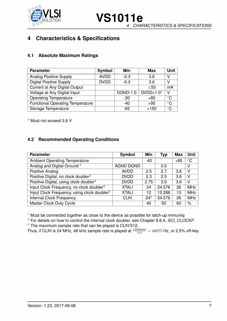
4.1 Absolute Maximum Ratings
Parameter Symbol Min Max UnitAnalog Positive Supply AVDD -0.3 3.6 VDigital Positive Supply DVDD -0.3 3.6 VCurrent at Any Digital Output ±50 mAVoltage at Any Digital Input DGND-1.0 DVDD+1.01 VOperating Temperature -30 +85 CFunctional Operating Temperature -40 +95 CStorage Temperature -65 +150 C
1 Must not exceed 3.6 V
4.2 Recommended Operating Conditions
Parameter Symbol Min Typ Max UnitAmbient Operating Temperature -40 +85 CAnalog and Digital Ground 1 AGND DGND 0.0 VPositive Analog AVDD 2.5 2.7 3.6 VPositive Digital, no clock doubler2 DVDD 2.3 2.5 3.6 VPositive Digital, using clock doubler2 DVDD 2.75 3.0 3.6 VInput Clock Frequency, no clock doubler2 XTALI 24 24.576 26 MHzInput Clock Frequency, using clock doubler2 XTALI 12 12.288 13 MHzInternal Clock Frequency CLKI 243 24.576 26 MHzMaster Clock Duty Cycle 40 50 60 %
1 Must be connected together as close to the device as possible for latch-up immunity.2 For details on how to control the internal clock doubler, see Chapter 8.6.4, SCI_CLOCKF.3 The maximum sample rate that can be played is CLKI/512.Thus, if CLKI is 24 MHz, 48 kHz sample rate is played at 24000000
512 = 46875 Hz, or 2.5% off-key.
Version: 1.23, 2017-09-08 7
VS1011e4 CHARACTERISTICS & SPECIFICATIONS
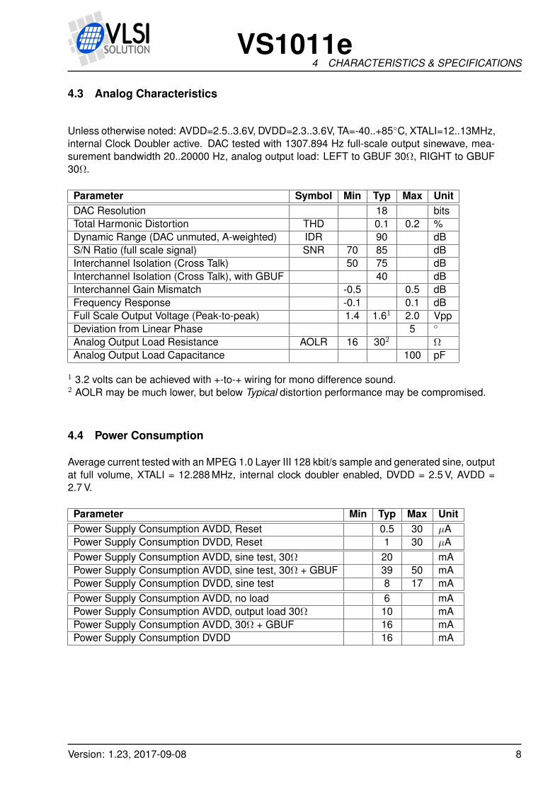
4.3 Analog Characteristics
Unless otherwise noted: AVDD=2.5..3.6V, DVDD=2.3..3.6V, TA=-40..+85C, XTALI=12..13MHz,internal Clock Doubler active. DAC tested with 1307.894 Hz full-scale output sinewave, mea-surement bandwidth 20..20000 Hz, analog output load: LEFT to GBUF 30Ω, RIGHT to GBUF30Ω.
Parameter Symbol Min Typ Max UnitDAC Resolution 18 bitsTotal Harmonic Distortion THD 0.1 0.2 %Dynamic Range (DAC unmuted, A-weighted) IDR 90 dBS/N Ratio (full scale signal) SNR 70 85 dBInterchannel Isolation (Cross Talk) 50 75 dBInterchannel Isolation (Cross Talk), with GBUF 40 dBInterchannel Gain Mismatch -0.5 0.5 dBFrequency Response -0.1 0.1 dBFull Scale Output Voltage (Peak-to-peak) 1.4 1.61 2.0 VppDeviation from Linear Phase 5
Analog Output Load Resistance AOLR 16 302 Ω
Analog Output Load Capacitance 100 pF
1 3.2 volts can be achieved with +-to-+ wiring for mono difference sound.2 AOLR may be much lower, but below Typical distortion performance may be compromised.
4.4 Power Consumption
Average current tested with an MPEG 1.0 Layer III 128 kbit/s sample and generated sine, outputat full volume, XTALI = 12.288 MHz, internal clock doubler enabled, DVDD = 2.5 V, AVDD =2.7 V.
Parameter Min Typ Max UnitPower Supply Consumption AVDD, Reset 0.5 30 µAPower Supply Consumption DVDD, Reset 1 30 µAPower Supply Consumption AVDD, sine test, 30Ω 20 mAPower Supply Consumption AVDD, sine test, 30Ω + GBUF 39 50 mAPower Supply Consumption DVDD, sine test 8 17 mAPower Supply Consumption AVDD, no load 6 mAPower Supply Consumption AVDD, output load 30Ω 10 mAPower Supply Consumption AVDD, 30Ω + GBUF 16 mAPower Supply Consumption DVDD 16 mA
Version: 1.23, 2017-09-08 8
VS1011e4 CHARACTERISTICS & SPECIFICATIONS
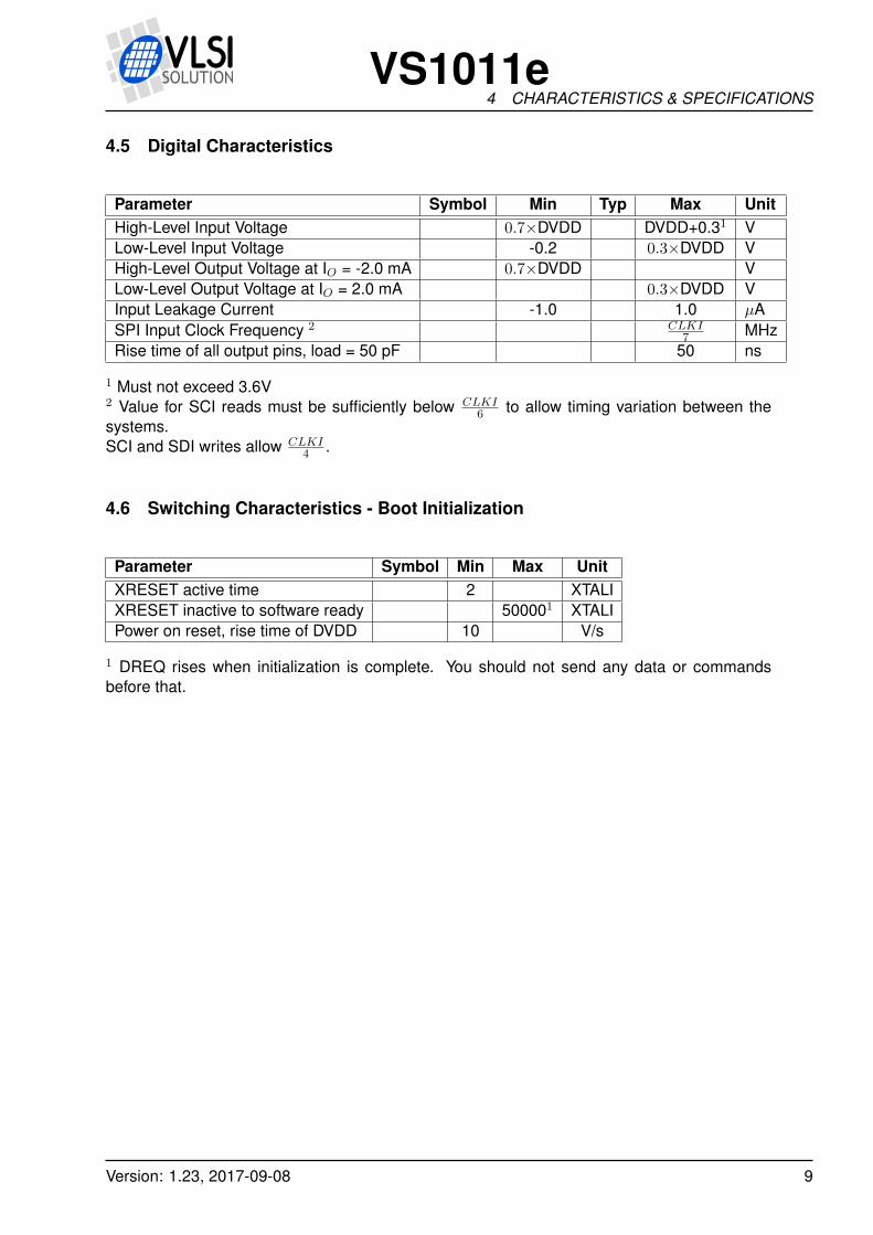
4.5 Digital Characteristics
Parameter Symbol Min Typ Max UnitHigh-Level Input Voltage 0.7×DVDD DVDD+0.31 VLow-Level Input Voltage -0.2 0.3×DVDD VHigh-Level Output Voltage at IO = -2.0 mA 0.7×DVDD VLow-Level Output Voltage at IO = 2.0 mA 0.3×DVDD VInput Leakage Current -1.0 1.0 µASPI Input Clock Frequency 2 CLKI
7 MHzRise time of all output pins, load = 50 pF 50 ns
1 Must not exceed 3.6V2 Value for SCI reads must be sufficiently below CLKI
6 to allow timing variation between thesystems.SCI and SDI writes allow CLKI
4 .
4.6 Switching Characteristics - Boot Initialization
Parameter Symbol Min Max UnitXRESET active time 2 XTALIXRESET inactive to software ready 500001 XTALIPower on reset, rise time of DVDD 10 V/s
1 DREQ rises when initialization is complete. You should not send any data or commandsbefore that.
Version: 1.23, 2017-09-08 9
VS1011e5 PACKAGES AND PIN DESCRIPTIONS
5 Packages and Pin Descriptions
5.1 Packages
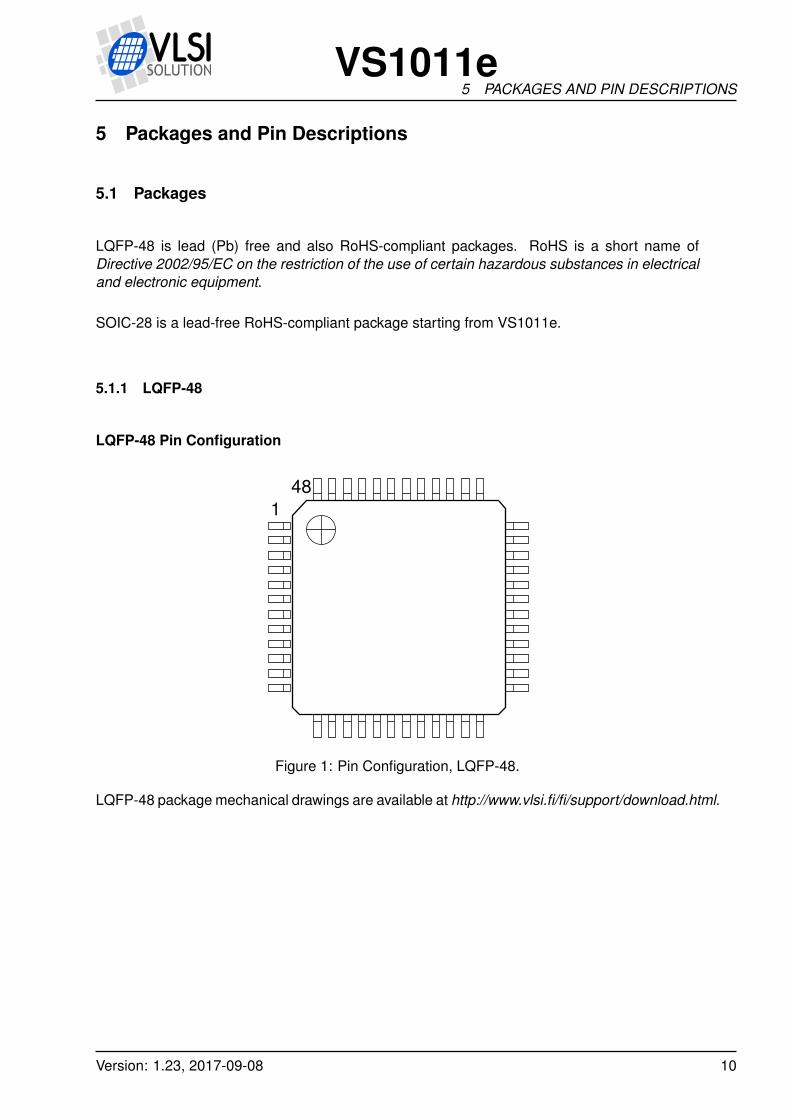
LQFP-48 is lead (Pb) free and also RoHS-compliant packages. RoHS is a short name ofDirective 2002/95/EC on the restriction of the use of certain hazardous substances in electricaland electronic equipment.
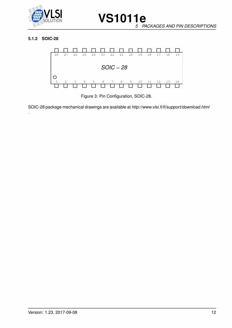
SOIC-28 is a lead-free RoHS-compliant package starting from VS1011e.
5.1.1 LQFP-48
LQFP-48 Pin Configuration
1
48
Figure 1: Pin Configuration, LQFP-48.
LQFP-48 package mechanical drawings are available at http://www.vlsi.fi/fi/support/download.html.
Version: 1.23, 2017-09-08 10
VS1011e5 PACKAGES AND PIN DESCRIPTIONS
LQFP-48 Package Outline
!
"
#
$ %
&
' '
( (
( %
( (
( %
! % % %
" %
# % %
$
& (
' '
)
*
)
*
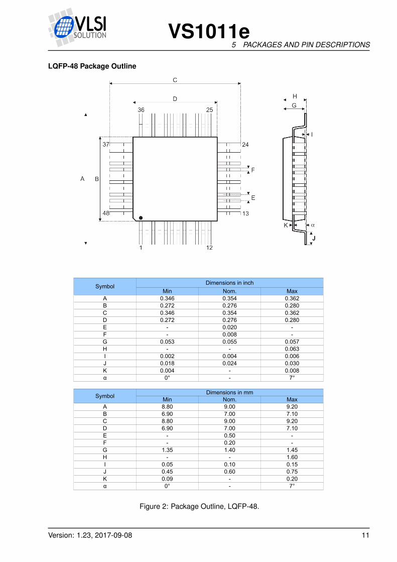
Figure 2: Package Outline, LQFP-48.
Version: 1.23, 2017-09-08 11
VS1011e5 PACKAGES AND PIN DESCRIPTIONS
5.1.2 SOIC-28
SOIC − 28
1413121110987654321
1516171819202122232728 26 2425
Figure 3: Pin Configuration, SOIC-28.
SOIC-28 package mechanical drawings are available at http://www.vlsi.fi/fi/support/download.html.
Version: 1.23, 2017-09-08 12
VS1011e5 PACKAGES AND PIN DESCRIPTIONS
5.2 Pin Descriptions
5.2.1 LQFP-48 Pin Descriptions
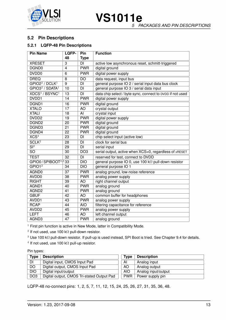
Pin Name LQFP-48
PinType
Function
XRESET 3 DI active low asynchronous reset, schmitt-triggeredDGND0 4 PWR digital groundDVDD0 6 PWR digital power supplyDREQ 8 DO data request, input busGPIO22 / DCLK1 9 DI general purpose IO 2 / serial input data bus clockGPIO32 / SDATA1 10 DI general purpose IO 3 / serial data inputXDCS4 / BSYNC1 13 DI data chip select / byte sync, connect to DVDD if not usedDVDD1 14 PWR digital power supplyDGND1 16 PWR digital groundXTALO 17 AO crystal outputXTALI 18 AI crystal inputDVDD2 19 PWR digital power supplyDGND2 20 PWR digital groundDGND3 21 PWR digital groundDGND4 22 PWR digital groundXCS4 23 DI chip select input (active low)SCLK2 28 DI clock for serial busSI2 29 DI serial inputSO 30 DO3 serial output, active when XCS=0, regardless of xRESET
TEST 32 DI reserved for test, connect to DVDDGPIO0 / SPIBOOT2,3 33 DIO general purpose IO 0, use 100 kΩ pull-down resistorGPIO12 34 DIO general purpose IO 1AGND0 37 PWR analog ground, low-noise referenceAVDD0 38 PWR analog power supplyRIGHT 39 AO right channel outputAGND1 40 PWR analog groundAGND2 41 PWR analog groundGBUF 42 AO common buffer for headphonesAVDD1 43 PWR analog power supplyRCAP 44 AIO filtering capacitance for referenceAVDD2 45 PWR analog power supplyLEFT 46 AO left channel outputAGND3 47 PWR analog ground
1 First pin function is active in New Mode, latter in Compatibility Mode.2 If not used, use 100 kΩ pull-down resistor.3 Use 100 kΩ pull-down resistor. If pull-up is used instead, SPI Boot is tried. See Chapter 9.4 for details.4 If not used, use 100 kΩ pull-up resistor.
Pin types:Type DescriptionDI Digital input, CMOS Input PadDO Digital output, CMOS Input PadDIO Digital input/outputDO3 Digital output, CMOS Tri-stated Output Pad
Type DescriptionAI Analog inputAO Analog outputAIO Analog input/outputPWR Power supply pin
LQFP-48 no-connect pins: 1, 2, 5, 7, 11, 12, 15, 24, 25, 26, 27, 31, 35, 36, 48.
Version: 1.23, 2017-09-08 13

VS1011e5 PACKAGES AND PIN DESCRIPTIONS
5.2.2 SOIC-28 Pin Descriptions
Pin Name Pin PinType
Function
DREQ 1 DO data request, input busGPIO22 / DCLK1 2 DIO serial input data bus clockGPIO32 / SDATA1 3 DI serial data inputXDCS4 / BSYNC1 4 DI byte synchronization signalDVDD1 5 PWR digital power supplyDGND1 6 PWR digital groundXTALO 7 CLK crystal outputXTALI 8 CLK crystal inputDVDD2 9 PWR digital power supplyDGND2 10 PWR digital groundXCS4 11 DI chip select input (active low)SCLK2 12 DI clock for serial busSI2 13 DI serial inputSO 14 DO3 serial output, active when XCS=0, regardless of XRESETTEST 15 DI reserved for test, connect to DVDDGPIO0 / SPIBOOT2,3 16 DIO general purpose IO 0, use 100 kΩ pull-down resistorGPIO12 17 DIO general purpose IO 1AGND0 18 PWR analog groundAVDD0 19 PWR analog power supplyRIGHT 20 AO right channel outputAGND2 21 PWR analog groundRCAP 22 AIO filtering capacitance for referenceAVDD2 23 PWR analog power supplyLEFT 24 AO left channel outputAGND3 25 PWR analog groundXRESET 26 DI active low asynchronous resetDGND0 27 PWR digital groundDVDD0 28 PWR digital power supply
1 First pin function is active in New Mode, latter in Compatibility Mode.2 If not used, use 100 kΩ pull-down resistor.3 Use 100 kΩ pull-down resistor. If pull-up is used instead, SPI Boot is tried. See Chapter 9.4 for details.4 If not used, use 100 kΩ pull-up resistor.
Pin types:
Type DescriptionDI Digital input, CMOS Input PadDO Digital output, CMOS Input PadDIO Digital input/outputDO3 Digital output, CMOS Tri-stated Output Pad
Type DescriptionAI Analog inputAO Analog outputAIO Analog input/outputPWR Power supply pin
Version: 1.23, 2017-09-08 14
VS1011e6 CONNECTION DIAGRAM, LQFP-48
6 Connection Diagram, LQFP-48
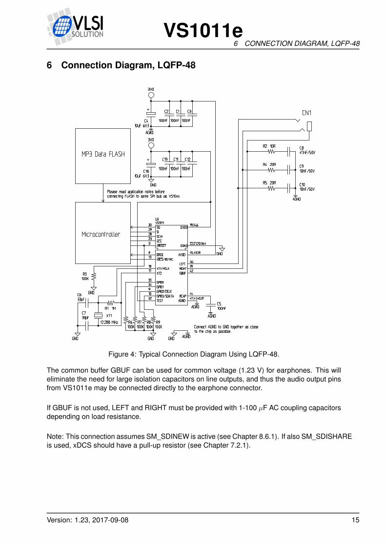
Figure 4: Typical Connection Diagram Using LQFP-48.
The common buffer GBUF can be used for common voltage (1.23 V) for earphones. This willeliminate the need for large isolation capacitors on line outputs, and thus the audio output pinsfrom VS1011e may be connected directly to the earphone connector.
If GBUF is not used, LEFT and RIGHT must be provided with 1-100 µF AC coupling capacitorsdepending on load resistance.
Note: This connection assumes SM_SDINEW is active (see Chapter 8.6.1). If also SM_SDISHAREis used, xDCS should have a pull-up resistor (see Chapter 7.2.1).
Version: 1.23, 2017-09-08 15
VS1011e7 SPI BUSES
7 SPI Buses
7.1 General
The SPI Bus - that was originally used in some Motorola devices - has been used for bothVS1011e’s Serial Data Interface SDI (Chapters 7.3 and 8.4) and Serial Control Interface SCI(Chapters 7.5 and 8.5).
7.2 SPI Bus Pin Descriptions
7.2.1 VS10xx Native Modes (New Mode, recommended)
These modes are active on VS1011e when SM_SDINEW is set to 1. DCLK and SDATA are notused for data transfer and they can be used as general-purpose I/O pins (GPIO2 and GPIO3).BSYNC function changes to data interface chip select (XDCS).
SDI Pin SCI Pin DescriptionXDCS XCS Active low chip select input. A high level forces the serial interface into
standby mode, ending the current operation. A high level also forces serialoutput (SO) to high impedance state. If SM_SDISHARE is 1, pin XDCSis not used, but the signal is generated internally by inverting XCS.
SCK Serial clock input. The serial clock is also used internally as the masterclock for the register interface.SCK can be gated or continuous. In either case, the first rising clock edgeafter XCS has gone low marks the first bit to be written.
SI Serial input. If a chip select is active, SI is sampled on the rising CLK edge.- SO Serial output. In reads, data is shifted out on the falling SCK edge.
In writes SO is at a high impedance state.
7.2.2 VS1001 Compatibility Mode (deprecated, do not use in new designs)
This mode is active when SM_SDINEW is 0 (default). In this mode, DCLK, SDATA and BSYNCare active.
SDI Pin SCI Pin Description- XCS Active low chip select input. A high level forces the serial interface into
standby mode, ending the current operation. A high level also forces serialoutput (SO) to high impedance state. There is no chip select for SDI, whichis always active.
BSYNC - SDI data is synchronized with a rising edge of BSYNC.DCLK SCK Serial clock input. The serial clock is also used internally as the master
clock for the register interface.SCK can be gated or continuous. In either case, the first rising clock edgeafter XCS has gone low marks the first bit to be written.
SDATA SI Serial input. SI is sampled on the rising SCK edge, if XCS is low.- SO Serial output. In reads, data is shifted out on the falling SCK edge.
In writes SO is at a high impedance state.
Version: 1.23, 2017-09-08 16
VS1011e7 SPI BUSES
7.3 Serial Protocol for Serial Data Interface (SDI)
7.3.1 General
The serial data interface operates in slave mode so the DCLK signal must be generated by anexternal circuit.
Data (SDATA signal) can be clocked in at either the rising or falling edge of DCLK (Chapter 8.6).
VS1011e assumes its data input to be byte-sychronized. SDI bytes may be transmitted eitherMSb or LSb first, depending of contents of SCI_MODE (Chapter 8.6).
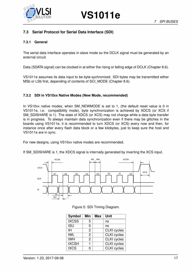
7.3.2 SDI in VS10xx Native Modes (New Mode, recommended)
In VS10xx native modes, when SM_NEWMODE is set to 1, (the default reset value is 0 inVS1011e, i.e. compatibility mode), byte synchronization is achieved by XDCS (or XCS ifSM_SDISHARE is 1). The state of XDCS (or XCS) may not change while a data byte transferis in progress. To always maintain data synchronization even if there may be glitches in theboards using VS1011e, it is recommended to turn XDCS (or XCS) every now and then, forinstance once after every flash data block or a few kilobytes, just to keep sure the host andVS1011e are in sync.
For new designs, using VS10xx native modes are recommended.
If SM_SDISHARE is 1, the XDCS signal is internally generated by inverting the XCS input.
SCK
SI
tXCSS tXCSHtWL tWH
tH
tSU
tXCS
xDCS
D7 D6 D5 D4 D3 D2 D1 D0
Figure 5: SDI Timing Diagram.
Symbol Min Max UnittXCSS 5 nstSU 0 nstH 2 CLKI cyclestWL 2 CLKI cyclestWH 2 CLKI cyclestXCSH 1 CLKI cyclestXCS 0 CLKI cycles
Version: 1.23, 2017-09-08 17
VS1011e7 SPI BUSES
Note: xDCS is not required to be deasserted between bytes, thus tXCS is 0.
Note: Although the timing is derived from the internal clock CLKI, the system always starts up in1.0× mode, thus CLKI=XTALI. After you have configured a higher clock through SCI_CLOCKFand waited for DREQ to rise, you can use a higher SPI speed as well.
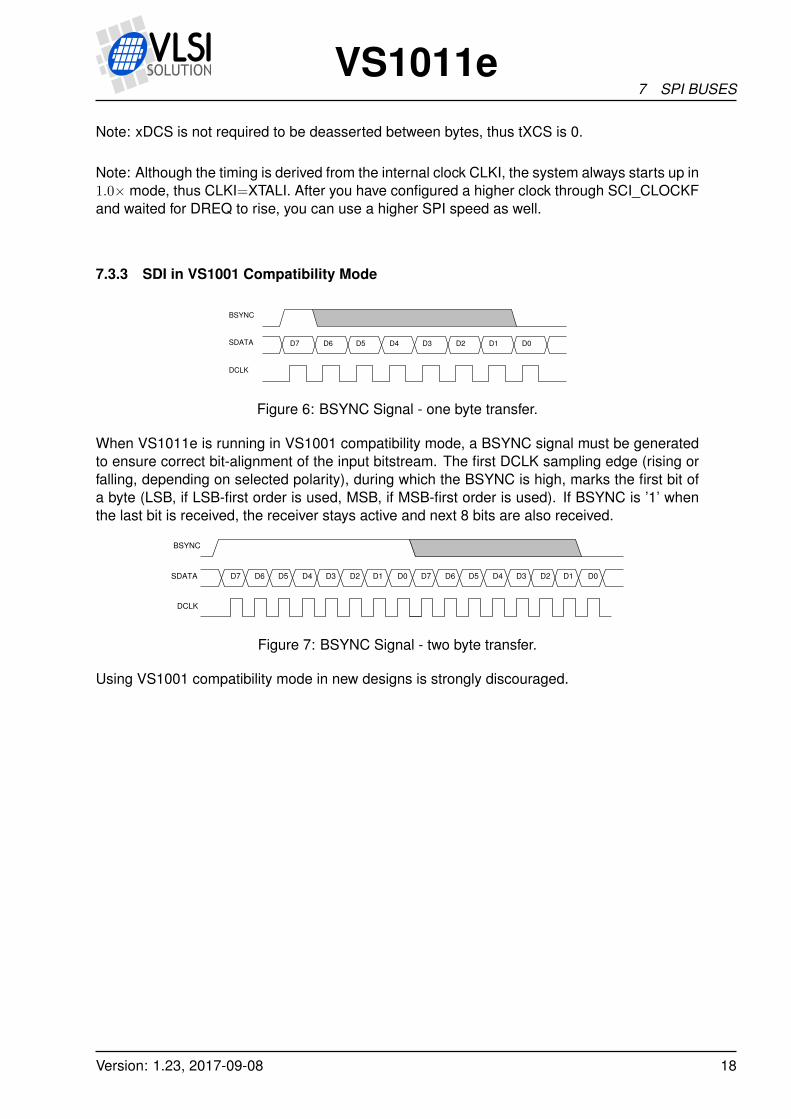
7.3.3 SDI in VS1001 Compatibility Mode
BSYNC
SDATA
DCLK
D7 D6 D5 D4 D3 D2 D1 D0
Figure 6: BSYNC Signal - one byte transfer.
When VS1011e is running in VS1001 compatibility mode, a BSYNC signal must be generatedto ensure correct bit-alignment of the input bitstream. The first DCLK sampling edge (rising orfalling, depending on selected polarity), during which the BSYNC is high, marks the first bit ofa byte (LSB, if LSB-first order is used, MSB, if MSB-first order is used). If BSYNC is ’1’ whenthe last bit is received, the receiver stays active and next 8 bits are also received.
BSYNC
SDATA
DCLK
D7 D6 D5 D4 D3 D2 D1 D0 D7 D6 D5 D4 D3 D2 D1 D0
Figure 7: BSYNC Signal - two byte transfer.
Using VS1001 compatibility mode in new designs is strongly discouraged.
Version: 1.23, 2017-09-08 18
VS1011e7 SPI BUSES
7.4 Data Request Pin DREQ
The DREQ pin/signal is used to signal if VS1011e’s FIFO is capable of receiving data. If DREQis high, VS1011e can take at least 32 bytes of SDI data or one SCI command. When thesecriteria are not met, DREQ is turned low, and the sender should stop transferring new data.
Because of a 32-byte safety area, the sender may send up to 32 bytes of SDI data at a timewithout checking the status of DREQ, making controlling VS1011e easier for low-speed micro-controllers.
Note: DREQ may turn low or high at any time, even during a byte transmission. Thus, DREQshould only be used to decide whether to send more bytes. It should not abort a transmissionthat has already started.
Note: In VS10XX products up to VS1002, DREQ was only used for SDI. In VS1011e DREQ isalso used to tell the status of SCI.
7.5 Serial Protocol for Serial Command Interface (SCI)
7.5.1 General
The serial bus protocol for the Serial Command Interface SCI (Chapter 8.5) consists of aninstruction byte, address byte and one 16-bit data word. Each read or write operation can reador write a single register. Data bits are read at the rising clock edge, so the user should updatedata at the falling clock edge. Bytes are always sent MSb firrst.
The operation is specified by an 8-bit instruction opcode. The supported instructions are readand write. See table below.
InstructionName Opcode OperationREAD 0000 0011 Read dataWRITE 0000 0010 Write data
Note: VS1011e sets DREQ low after each SCI operation. The duration depends on the opera-tion. It is not allowed to start a new SCI/SDI operation before DREQ is high again.
Version: 1.23, 2017-09-08 19
VS1011e7 SPI BUSES
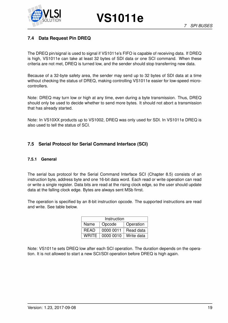
7.5.2 SCI Read
0 1 2 3 4 5 6 7 8 9 10 11 12 13 30 3114 15 16 17
0 0 0 0 0 0 1 1 0 0 0 0
3 2 1 0
0 0 0 0 0 0 0 0 0 0 0 0 0 0 0 0
15 14 1 0
X
instruction (read) addressdata out
XCS
SCK
SI
SO
don’t care don’t care
DREQ
execution
Figure 8: SCI Word Read
VS1011e registers are read by the following sequence, as shown in Figure 8. First, XCS lineis pulled low to select the device. Then the READ opcode (0x3) is transmitted via the SI linefollowed by an 8-bit word address. After the address has been read in, any further data on SIis ignored. The 16-bit data corresponding to the received address will be shifted out onto theSO line.
XCS should be driven high after data has been shifted out.
DREQ is driven low for a short while when in a read operation by the chip. This is a very shorttime and doesn’t require special user attention.
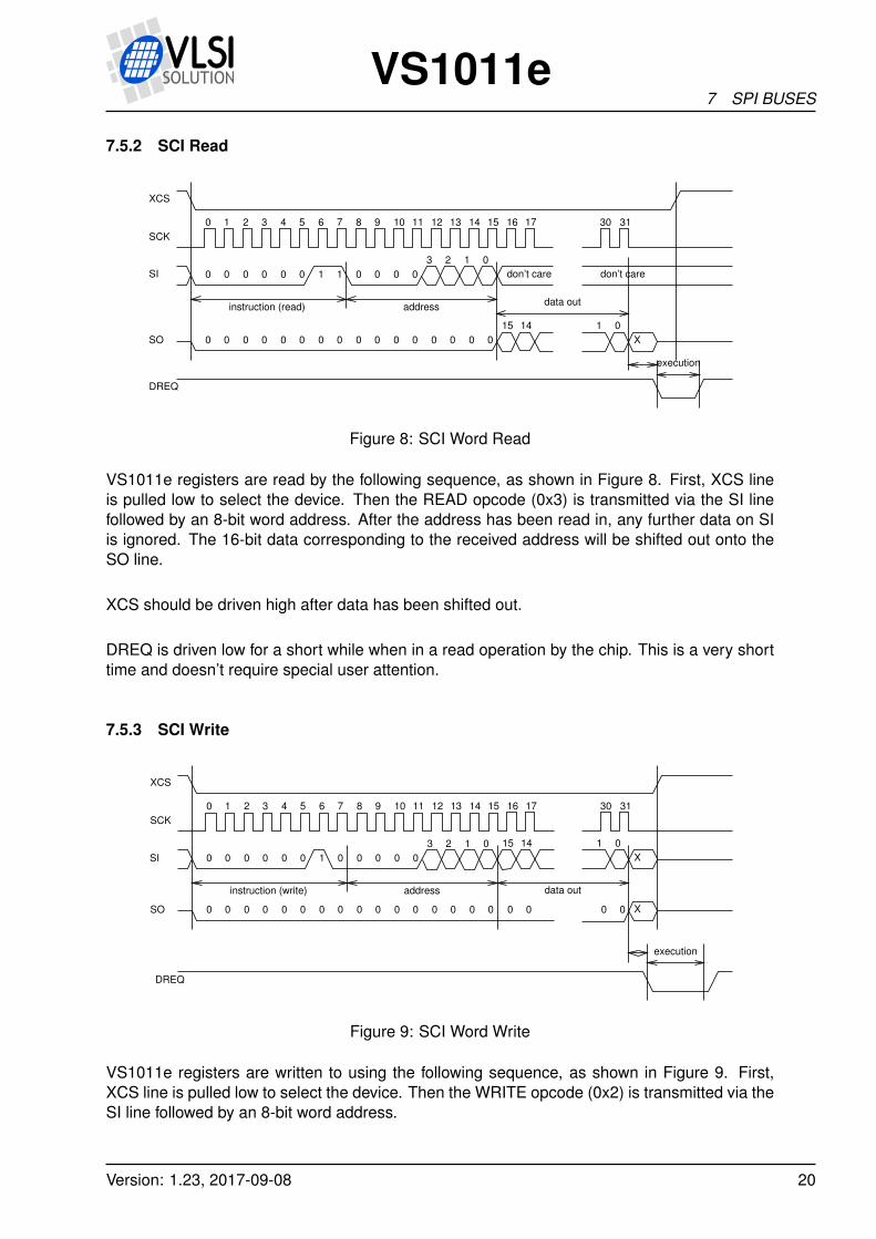
7.5.3 SCI Write
0 1 2 3 4 5 6 7 8 9 10 11 12 13 30 3114 15 16 17
0 0 0 0 0 0 1 0 0 0 0
3 2 1 0 1 0
X
address
XCS
SCK
SI
15 14
data out
0 0 0 0 0 0 0 0 0 0 0 0 0 0 0 0SO 0 0 0 0 X
0
instruction (write)
DREQ
execution
Figure 9: SCI Word Write
VS1011e registers are written to using the following sequence, as shown in Figure 9. First,XCS line is pulled low to select the device. Then the WRITE opcode (0x2) is transmitted via theSI line followed by an 8-bit word address.
Version: 1.23, 2017-09-08 20
VS1011e7 SPI BUSES
After the word has been shifted in and the last clock has been sent, XCS should be pulled highto end the WRITE sequence.
After the last bit has been sent, DREQ is driven low for the duration of the register update,marked “execution” in the figure. The time varies depending on the register and its contents(see table in Chapter 8.6 for details). If the maximum time is longer than what it takes fromthe microcontroller to feed the next SCI command or SDI byte, it is not allowed to finish a newSCI/SDI operation before DREQ has risen up again.
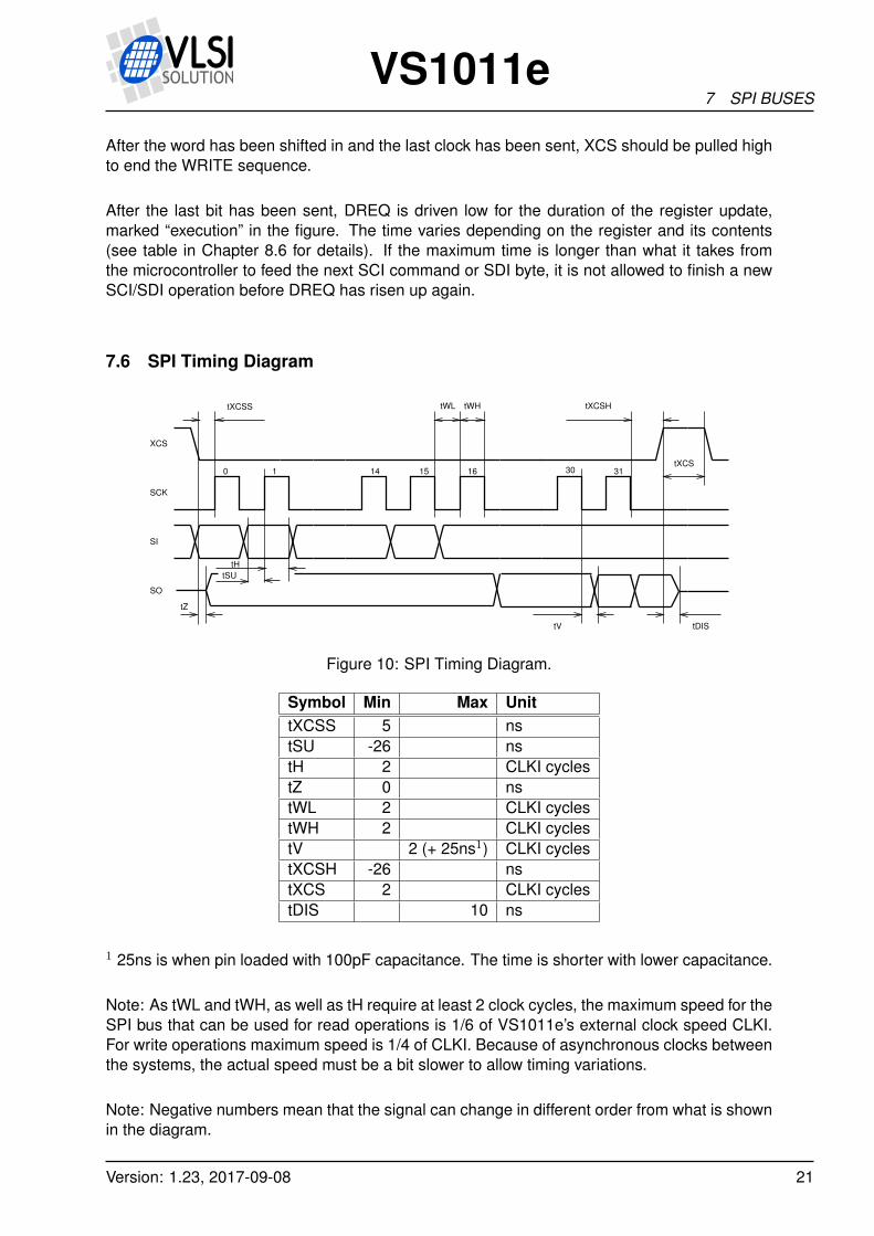
7.6 SPI Timing Diagram
XCS
SCK
SI
SO
0 1 1514 16
tXCSS tXCSHtWL tWH
tH
tSU
tV
tZ
tDIS
tXCS30 31
Figure 10: SPI Timing Diagram.
Symbol Min Max UnittXCSS 5 nstSU -26 nstH 2 CLKI cyclestZ 0 nstWL 2 CLKI cyclestWH 2 CLKI cyclestV 2 (+ 25ns1) CLKI cyclestXCSH -26 nstXCS 2 CLKI cyclestDIS 10 ns
1 25ns is when pin loaded with 100pF capacitance. The time is shorter with lower capacitance.
Note: As tWL and tWH, as well as tH require at least 2 clock cycles, the maximum speed for theSPI bus that can be used for read operations is 1/6 of VS1011e’s external clock speed CLKI.For write operations maximum speed is 1/4 of CLKI. Because of asynchronous clocks betweenthe systems, the actual speed must be a bit slower to allow timing variations.
Note: Negative numbers mean that the signal can change in different order from what is shownin the diagram.
Version: 1.23, 2017-09-08 21
VS1011e7 SPI BUSES
7.7 SPI Examples with SM_SDINEW and SM_SDISHARED set
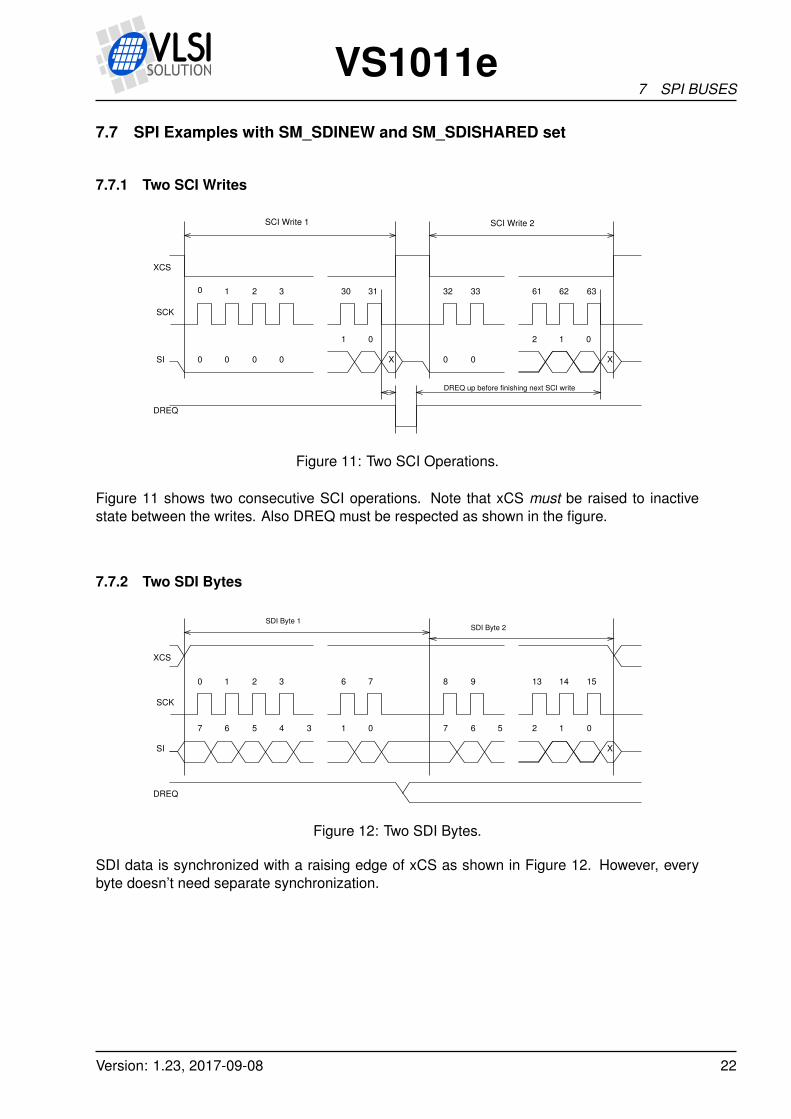
7.7.1 Two SCI Writes
0 1 2 3 30 31
1 0 1 0
0 0 0 0 0 0X X
XCS
SCK
SI
2
32 33 61 62 63
SCI Write 1 SCI Write 2
DREQ
DREQ up before finishing next SCI write
Figure 11: Two SCI Operations.
Figure 11 shows two consecutive SCI operations. Note that xCS must be raised to inactivestate between the writes. Also DREQ must be respected as shown in the figure.
7.7.2 Two SDI Bytes
1 2 3
XCS
SCK
SI
7 6 5 4 3 1 0 7 6 5 2 1 0
X
SDI Byte 1SDI Byte 2
0 6 7 8 9 13 14 15
DREQ
Figure 12: Two SDI Bytes.
SDI data is synchronized with a raising edge of xCS as shown in Figure 12. However, everybyte doesn’t need separate synchronization.
Version: 1.23, 2017-09-08 22
VS1011e7 SPI BUSES
7.7.3 SCI Operation in Middle of Two SDI Bytes
0 1
XCS
SCK
SI
7
7 6 5 1
0 0
0 7 6 5 1 0
SDI ByteSCI Operation
SDI Byte
8 9 39 40 41 46 47
X
DREQ high before end of next transfer
DREQ
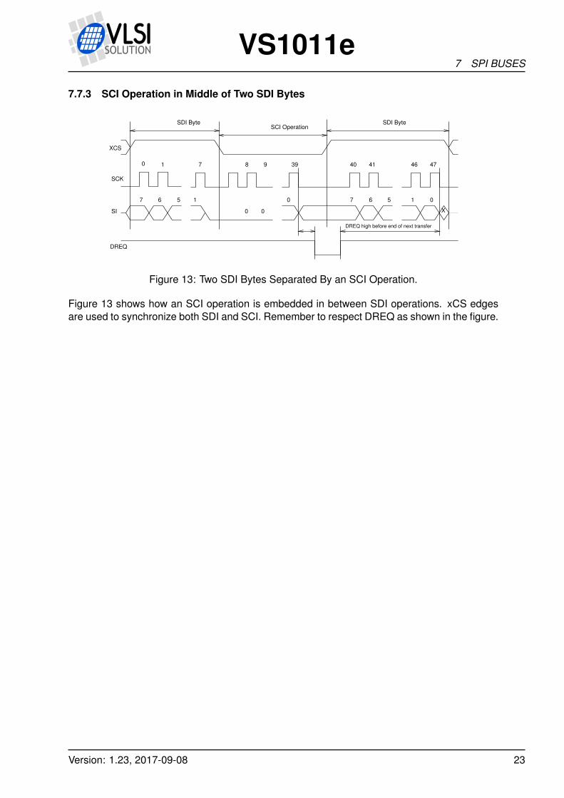
Figure 13: Two SDI Bytes Separated By an SCI Operation.
Figure 13 shows how an SCI operation is embedded in between SDI operations. xCS edgesare used to synchronize both SDI and SCI. Remember to respect DREQ as shown in the figure.
Version: 1.23, 2017-09-08 23
VS1011e8 FUNCTIONAL DESCRIPTION
8 Functional Description
8.1 Main Features
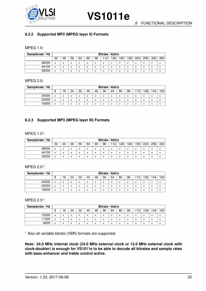
VS1011e is based on a proprietary digital signal processor, VS_DSP. It contains all the codeand data memory needed for MPEG, WAV PCM and WAV IMA ADPCM audio decoding, to-gether with serial interfaces, a multirate stereo audio DAC and analog output amplifiers andfilters.
VS1011e can play all MPEG 1.0, and 2.0 layer I, II and III files, as well as MPEG 2.5 layer IIIfiles, with all sample rates and bitrates, including variable bitrate (VBR) for layer III. Note, thatdecoding of layers I and II must be activated separately.
8.2 Supported Audio Codecs
ConventionsMark Description+ Format is supported- Format exists but is not supported? Format not tested
Format doesn’t exist
8.2.1 Supported MP1 (MPEG layer I) Formats
MPEG 1.0:
Samplerate / Hz Bitrate / kbit/s32 64 96 128 160 192 224 256 288 320 352 384 416 448
48000 + + + + + + + + + + + + + +44100 + + + + + + + + + + + + + +32000 + + + + + + + + + + + + + +
MPEG 2.0:
Samplerate / Hz Bitrate / kbit/s32 48 56 64 80 96 112 128 144 160 176 192 224 256
24000 ? ? ? ? ? ? ? ? ? ? ? ? ? ?22050 ? ? ? ? ? ? ? ? ? ? ? ? ? ?16000 ? ? ? ? ? ? ? ? ? ? ? ? ? ?
Version: 1.23, 2017-09-08 24
VS1011e8 FUNCTIONAL DESCRIPTION
8.2.2 Supported MP2 (MPEG layer II) Formats
MPEG 1.0:
Samplerate / Hz Bitrate / kbit/s32 48 56 64 80 96 112 128 160 192 224 256 320 384
48000 + + + + + + + + + + + + + +44100 + + + + + + + + + + + + + +32000 + + + + + + + + + + + + + +
MPEG 2.0:
Samplerate / Hz Bitrate / kbit/s8 16 24 32 40 48 56 64 80 96 112 128 144 160
24000 + + + + + + + + + + + + + +22050 + + + + + + + + + + + + + +16000 + + + + + + + + + + + + + +
8.2.3 Supported MP3 (MPEG layer III) Formats
MPEG 1.01:
Samplerate / Hz Bitrate / kbit/s32 40 48 56 64 80 96 112 128 160 192 224 256 320
48000 + + + + + + + + + + + + + +44100 + + + + + + + + + + + + + +32000 + + + + + + + + + + + + + +
MPEG 2.01:
Samplerate / Hz Bitrate / kbit/s8 16 24 32 40 48 56 64 80 96 112 128 144 160
24000 + + + + + + + + + + + + + +22050 + + + + + + + + + + + + + +16000 + + + + + + + + + + + + + +
MPEG 2.51:
Samplerate / Hz Bitrate / kbit/s8 16 24 32 40 48 56 64 80 96 112 128 144 160
12000 + + + + + + + + + + + + + +11025 + + + + + + + + + + + + + +
8000 + + + + + + + + + + + + + +
1 Also all variable bitrate (VBR) formats are supported.
Note: 24.0 MHz internal clock (24.0 MHz external clock or 12.0 MHz external clock withclock-doubler) is enough for VS1011e to be able to decode all bitrates and sample rateswith bass enhancer and treble control active.
Version: 1.23, 2017-09-08 25
VS1011e8 FUNCTIONAL DESCRIPTION
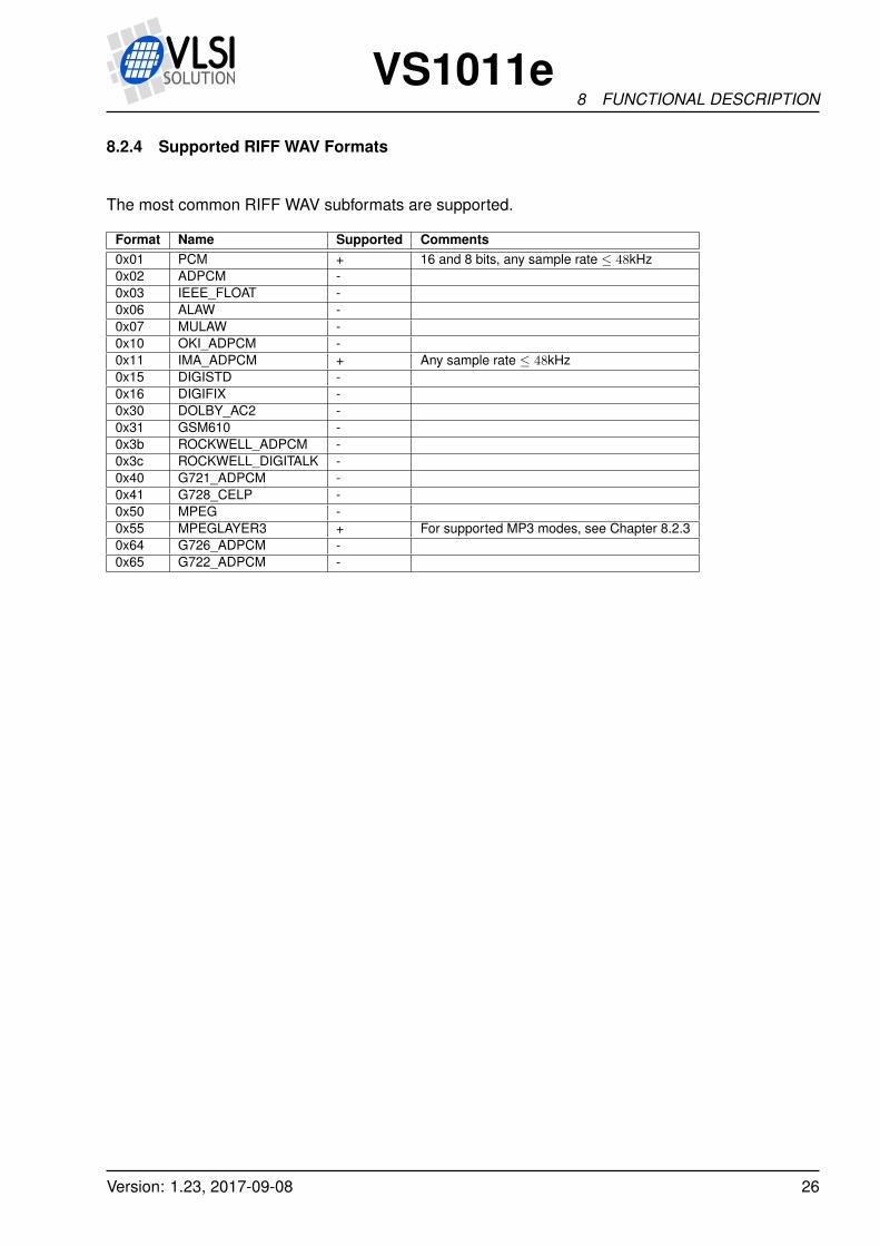
8.2.4 Supported RIFF WAV Formats
The most common RIFF WAV subformats are supported.
Format Name Supported Comments0x01 PCM + 16 and 8 bits, any sample rate ≤ 48kHz0x02 ADPCM -0x03 IEEE_FLOAT -0x06 ALAW -0x07 MULAW -0x10 OKI_ADPCM -0x11 IMA_ADPCM + Any sample rate ≤ 48kHz0x15 DIGISTD -0x16 DIGIFIX -0x30 DOLBY_AC2 -0x31 GSM610 -0x3b ROCKWELL_ADPCM -0x3c ROCKWELL_DIGITALK -0x40 G721_ADPCM -0x41 G728_CELP -0x50 MPEG -0x55 MPEGLAYER3 + For supported MP3 modes, see Chapter 8.2.30x64 G726_ADPCM -0x65 G722_ADPCM -
Version: 1.23, 2017-09-08 26
VS1011e8 FUNCTIONAL DESCRIPTION
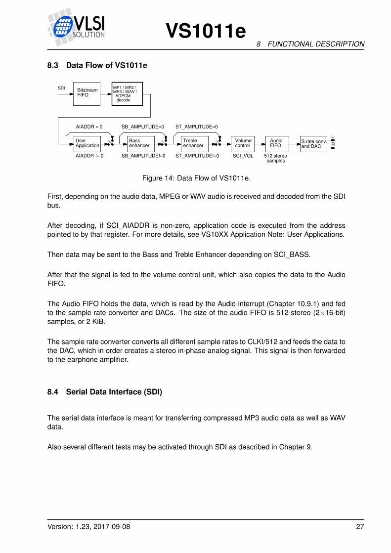
8.3 Data Flow of VS1011e
Volumecontrol
AudioFIFO
S.rate.conv.and DAC R
BitstreamFIFO
SDI
L
SCI_VOL
Bassenhancer
SB_AMPLITUDE=0
SB_AMPLITUDE!=0
AIADDR = 0
AIADDR != 0
UserApplication
ST_AMPLITUDE=0
ST_AMPLITUDE!=0
Trebleenhancer
MP1 / MP2 /MP3 / WAV / ADPCM decode
512 stereo samples
Figure 14: Data Flow of VS1011e.
First, depending on the audio data, MPEG or WAV audio is received and decoded from the SDIbus.
After decoding, if SCI_AIADDR is non-zero, application code is executed from the addresspointed to by that register. For more details, see VS10XX Application Note: User Applications.
Then data may be sent to the Bass and Treble Enhancer depending on SCI_BASS.
After that the signal is fed to the volume control unit, which also copies the data to the AudioFIFO.
The Audio FIFO holds the data, which is read by the Audio interrupt (Chapter 10.9.1) and fedto the sample rate converter and DACs. The size of the audio FIFO is 512 stereo (2×16-bit)samples, or 2 KiB.
The sample rate converter converts all different sample rates to CLKI/512 and feeds the data tothe DAC, which in order creates a stereo in-phase analog signal. This signal is then forwardedto the earphone amplifier.
8.4 Serial Data Interface (SDI)
The serial data interface is meant for transferring compressed MP3 audio data as well as WAVdata.
Also several different tests may be activated through SDI as described in Chapter 9.
Version: 1.23, 2017-09-08 27
VS1011e8 FUNCTIONAL DESCRIPTION
8.5 Serial Control Interface (SCI)
The serial control interface is compatible with the SPI bus specification. Data transfers arealways 16 bits. VS1011e is controlled by writing and reading the registers of the interface.
The main controls of the control interface are:
• control of the operation mode, clock, and builtin effects• access to status information and header data• access to encoded digital data• uploading user programs• feeding input data
8.6 SCI Registers
SCI registers, prefix SCI_Reg Type Reset Time1 Abbrev[bits] Description0x0 rw 0 70 CLKI4 MODE Mode control0x1 rw 0x2C3 40 CLKI STATUS Status of VS1011e0x2 rw 0 2100 CLKI BASS Built-in bass/treble enhancer0x3 rw 0 80 XTALI CLOCKF Clock freq + multiplier0x4 rw 0 40 CLKI DECODE_TIME Decode time in seconds0x5 rw 0 3200 CLKI AUDATA Misc. audio data0x6 rw 0 80 CLKI WRAM RAM write/read0x7 rw 0 80 CLKI WRAMADDR Base address for RAM
write/read0x8 r 0 - HDAT0 Stream header data 00x9 r 0 - HDAT1 Stream header data 10xA rw 0 3200 CLKI2 AIADDR Start address of application0xB rw 0 2100 CLKI VOL Volume control0xC rw 0 50 CLKI2 AICTRL0 Application control register 00xD rw 0 50 CLKI2 AICTRL1 Application control register 10xE rw 0 50 CLKI2 AICTRL2 Application control register 20xF rw 0 50 CLKI2 AICTRL3 Application control register 3
1 This is the worst-case time that DREQ stays low after writing to this register. The user maychoose to skip the DREQ check for those register writes that take less than 100 clock cycles toexecute.
2 In addition, the cycles spent in the user application routine must be counted.
3 Firmware changes the value of this register immediately to 0x28, and in less than 100 ms to0x20.
4 When mode register write specifies a software reset the worst-case time is 9600 XTALI cycles.
Note that if DREQ is low when an SCI write is done, DREQ also stays low after SCI writeprocessing.
Version: 1.23, 2017-09-08 28
VS1011e8 FUNCTIONAL DESCRIPTION
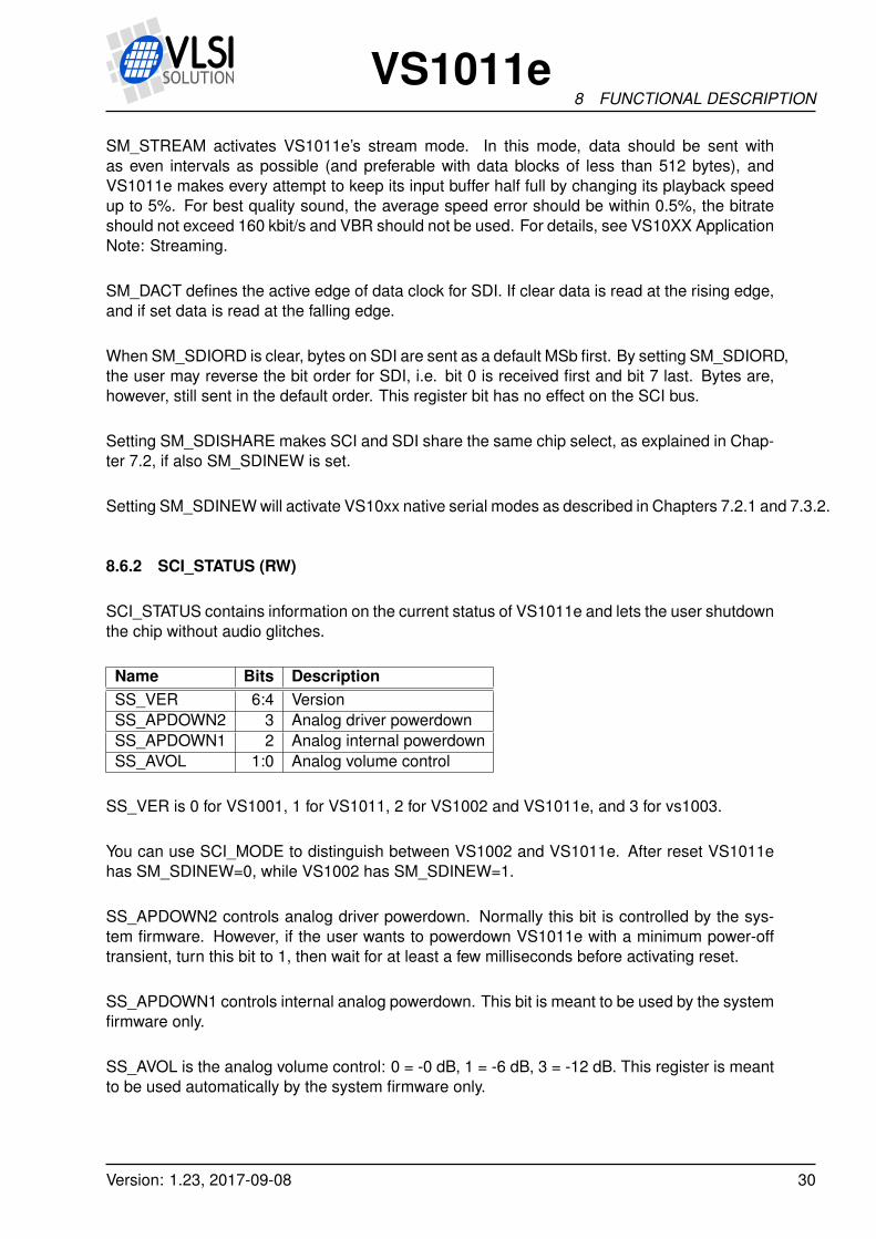
8.6.1 SCI_MODE (RW)
SCI_MODE is used to control operation of VS1011e.
Bit Name Function Value Description0 SM_DIFF Differential 0 normal in-phase audio
1 left channel inverted1 SM_LAYER12 Allow MPEG layers I & II 0 no
1 yes2 SM_RESET Soft reset 0 no reset
1 reset3 SM_OUTOFWAV Jump out of WAV decoding 0 no
1 yes4 SM_SETTOZERO1 set to zero 0 right
1 wrong5 SM_TESTS Allow SDI tests 0 not allowed
1 allowed6 SM_STREAM Stream mode 0 no
1 yes7 SM_SETTOZERO2 set to zero 0 right
1 wrong8 SM_DACT DCLK active edge 0 rising
1 falling9 SM_SDIORD SDI bit order 0 MSb first
1 MSb last10 SM_SDISHARE Share SPI chip select 0 no
1 yes11 SM_SDINEW VS10xx native SPI modes 0 no
1 yes12 SM_SETTOZERO3 set to zero 0 right
1 wrong13 SM_SETTOZERO4 set to zero 0 right
1 wrong
When SM_DIFF is set, the player inverts the left channel output. For a stereo input this createsa virtual surround, and for a mono input this effectively creates a differential left/right signal.
SM_LAYER12 determines whether it is allowed to decode MPEG 1 and 2 layers I and II inaddition to layer III.
By setting SM_RESET to 1, the player is software reset. This bit clears automatically.
When the user decoding a WAV file wants to get out of the file without playing it to the end, setSM_OUTOFWAV, and send zeros to VS1002e until SM_OUTOFWAV is again zero. If the userdoesn’t want to check SM_OUTOFWAV, send 128 zeros.
If SM_TESTS is set, SDI tests are allowed. For more details on SDI tests, look at Chapter 9.7.
Version: 1.23, 2017-09-08 29
VS1011e8 FUNCTIONAL DESCRIPTION
SM_STREAM activates VS1011e’s stream mode. In this mode, data should be sent withas even intervals as possible (and preferable with data blocks of less than 512 bytes), andVS1011e makes every attempt to keep its input buffer half full by changing its playback speedup to 5%. For best quality sound, the average speed error should be within 0.5%, the bitrateshould not exceed 160 kbit/s and VBR should not be used. For details, see VS10XX ApplicationNote: Streaming.
SM_DACT defines the active edge of data clock for SDI. If clear data is read at the rising edge,and if set data is read at the falling edge.
When SM_SDIORD is clear, bytes on SDI are sent as a default MSb first. By setting SM_SDIORD,the user may reverse the bit order for SDI, i.e. bit 0 is received first and bit 7 last. Bytes are,however, still sent in the default order. This register bit has no effect on the SCI bus.
Setting SM_SDISHARE makes SCI and SDI share the same chip select, as explained in Chap-ter 7.2, if also SM_SDINEW is set.
Setting SM_SDINEW will activate VS10xx native serial modes as described in Chapters 7.2.1 and 7.3.2.
8.6.2 SCI_STATUS (RW)
SCI_STATUS contains information on the current status of VS1011e and lets the user shutdownthe chip without audio glitches.
Name Bits DescriptionSS_VER 6:4 VersionSS_APDOWN2 3 Analog driver powerdownSS_APDOWN1 2 Analog internal powerdownSS_AVOL 1:0 Analog volume control
SS_VER is 0 for VS1001, 1 for VS1011, 2 for VS1002 and VS1011e, and 3 for vs1003.
You can use SCI_MODE to distinguish between VS1002 and VS1011e. After reset VS1011ehas SM_SDINEW=0, while VS1002 has SM_SDINEW=1.
SS_APDOWN2 controls analog driver powerdown. Normally this bit is controlled by the sys-tem firmware. However, if the user wants to powerdown VS1011e with a minimum power-offtransient, turn this bit to 1, then wait for at least a few milliseconds before activating reset.
SS_APDOWN1 controls internal analog powerdown. This bit is meant to be used by the systemfirmware only.
SS_AVOL is the analog volume control: 0 = -0 dB, 1 = -6 dB, 3 = -12 dB. This register is meantto be used automatically by the system firmware only.
Version: 1.23, 2017-09-08 30
VS1011e8 FUNCTIONAL DESCRIPTION
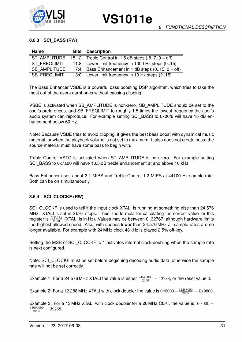
8.6.3 SCI_BASS (RW)
Name Bits DescriptionST_AMPLITUDE 15:12 Treble Control in 1.5 dB steps (-8..7, 0 = off)ST_FREQLIMIT 11:8 Lower limit frequency in 1000 Hz steps (0..15)SB_AMPLITUDE 7:4 Bass Enhancement in 1 dB steps (0..15, 0 = off)SB_FREQLIMIT 3:0 Lower limit frequency in 10 Hz steps (2..15)
The Bass Enhancer VSBE is a powerful bass boosting DSP algorithm, which tries to take themost out of the users earphones without causing clipping.
VSBE is activated when SB_AMPLITUDE is non-zero. SB_AMPLITUDE should be set to theuser’s preferences, and SB_FREQLIMIT to roughly 1.5 times the lowest frequency the user’saudio system can reproduce. For example setting SCI_BASS to 0x00f6 will have 15 dB en-hancement below 60 Hz.
Note: Because VSBE tries to avoid clipping, it gives the best bass boost with dynamical musicmaterial, or when the playback volume is not set to maximum. It also does not create bass: thesource material must have some bass to begin with.
Treble Control VSTC is activated when ST_AMPLITUDE is non-zero. For example settingSCI_BASS to 0x7a00 will have 10.5 dB treble enhancement at and above 10 kHz.
Bass Enhancer uses about 2.1 MIPS and Treble Control 1.2 MIPS at 44100 Hz sample rate.Both can be on simultaneously.
8.6.4 SCI_CLOCKF (RW)
SCI_CLOCKF is used to tell if the input clock XTALI is running at something else than 24.576MHz. XTALI is set in 2 kHz steps. Thus, the formula for calculating the correct value for thisregister is XTALI
2000 (XTALI is in Hz). Values may be between 0..32767, although hardware limitsthe highest allowed speed. Also, with speeds lower than 24.576 MHz all sample rates are nolonger available. For example with 24 MHz clock 48 kHz is played 2.5% off-key.
Setting the MSB of SCI_CLOCKF to 1 activates internal clock-doubling when the sample rateis next configured.
Note: SCI_CLOCKF must be set before beginning decoding audio data; otherwise the samplerate will not be set correctly.
Example 1: For a 24.576 MHz XTALI the value is either 245760002000 = 12288, or the reset value 0.
Example 2: For a 12.288 MHz XTALI with clock doubler the value is 0x8000+ 122880002000 = 0x9800.
Example 3: For a 13 MHz XTALI with clock doubler for a 26 MHz CLKI, the value is 0x8000 +13000000
2000 = 39268.
Version: 1.23, 2017-09-08 31
VS1011e8 FUNCTIONAL DESCRIPTION
8.6.5 SCI_DECODE_TIME (RW)
When decoding correct data, current decoded time is shown in this register in full seconds.
The user may change the value of this register. However, in that case the new value should bewritten twice.
SCI_DECODE_TIME is reset at every software reset.
8.6.6 SCI_AUDATA (RW)
When decoding correct data, the current sample rate and number of channels can be found inbits 15:1 and 0 of SCI_AUDATA, respectively. Bits 15:1 contain the sample rate divided by two,and bit 0 is 0 for mono data and 1 for stereo. Writing to this register will change the sample rateon the run to the number given.
Example: 44100 Hz stereo data reads as 0xAC45 (44101).Example: 11025 Hz mono data reads as 0x2B10 (11024).Example: Writing 0xAC80 sets sample rate to 44160 Hz, stereo mode does not change.
8.6.7 SCI_WRAM (RW)
SCI_WRAM is used to upload application programs and data to instruction and data RAMs.The start address must be initialized by writing to SCI_WRAMADDR prior to the first write/readof SCI_WRAM. As 16 bits of data can be transferred with one SCI_WRAM write/read, and theinstruction word is 32 bits long, two consecutive writes/reads are needed for each instructionword. The byte order is big-endian (i.e. MSBs first). After each full-word write/read, the internalpointer is autoincremented.
8.6.8 SCI_WRAMADDR (RW)
SCI_WRAMADDR is used to set the program address and memory bus for following SCI_WRAMwrites/reads.
SM_WRAMADDR Dest. addr. Bits/ DescriptionStart. . . End Start. . . End Word0x1380. . . 0x13FF 0x1380. . . 0x13FF 16 X data RAM0x4780. . . 0x47FF 0x0780. . . 0x07FF 16 Y data RAM0x8030. . . 0x84FF 0x0030. . . 0x04FF 32 Instruction RAM0xC000. . . 0xFFFF 0xC000. . . 0xFFFF 16 I/O
Version: 1.23, 2017-09-08 32
VS1011e8 FUNCTIONAL DESCRIPTION
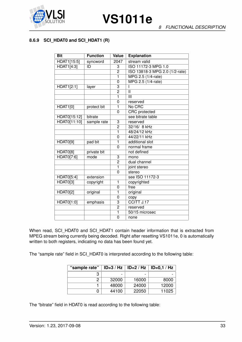
8.6.9 SCI_HDAT0 and SCI_HDAT1 (R)
Bit Function Value ExplanationHDAT1[15:5] syncword 2047 stream validHDAT1[4:3] ID 3 ISO 11172-3 MPG 1.0
2 ISO 13818-3 MPG 2.0 (1/2-rate)1 MPG 2.5 (1/4-rate)0 MPG 2.5 (1/4-rate)
HDAT1[2:1] layer 3 I2 II1 III0 reserved
HDAT1[0] protect bit 1 No CRC0 CRC protected
HDAT0[15:12] bitrate see bitrate tableHDAT0[11:10] sample rate 3 reserved
2 32/16/ 8 kHz1 48/24/12 kHz0 44/22/11 kHz
HDAT0[9] pad bit 1 additional slot0 normal frame
HDAT0[8] private bit not definedHDAT0[7:6] mode 3 mono
2 dual channel1 joint stereo0 stereo
HDAT0[5:4] extension see ISO 11172-3HDAT0[3] copyright 1 copyrighted
0 freeHDAT0[2] original 1 original
0 copyHDAT0[1:0] emphasis 3 CCITT J.17
2 reserved1 50/15 microsec0 none
When read, SCI_HDAT0 and SCI_HDAT1 contain header information that is extracted fromMPEG stream being currently being decoded. Right after resetting VS1011e, 0 is automaticallywritten to both registers, indicating no data has been found yet.
The “sample rate” field in SCI_HDAT0 is interpreted according to the following table:
“sample rate” ID=3 / Hz ID=2 / Hz ID=0,1 / Hz3 - - -2 32000 16000 80001 48000 24000 120000 44100 22050 11025
The “bitrate” field in HDAT0 is read according to the following table:
Version: 1.23, 2017-09-08 33
VS1011e8 FUNCTIONAL DESCRIPTION
Layer I Layer II Layer III“bitrate” ID=3 ID=0,1,2 ID=3 ID=0,1,2 ID=3 ID=0,1,2
kbit/s kbit/s kbit/s15 forbidden forbidden forbidden forbidden forbidden forbidden14 448 256 384 160 320 16013 416 224 320 144 256 14412 384 192 256 128 224 12811 352 176 224 112 192 11210 320 160 192 96 160 96
9 288 144 160 80 128 808 256 128 128 64 112 647 224 112 112 56 96 566 192 96 96 48 80 485 160 80 80 40 64 404 128 64 64 32 56 323 96 56 56 24 48 242 64 48 48 16 40 161 32 32 32 8 32 80 - - - - - -
When decoding a WAV file, SPI_HDAT0 and SPI_HDAT1 read as 0x7761 and 0x7665, respec-tively.
8.6.10 SCI_AIADDR (RW)
SCI_AIADDR indicates the start address of the application code written earlier with SCI_WRAMADDRand SCI_WRAM registers. If no application code is used, this register should not be initialized,or it should be initialized to zero. For more details, see VS10XX Application Note: User Appli-cations.
8.6.11 SCI_VOL (RW)
SCI_VOL is a volume control for the player hardware. For each channel, a value in the range of0..254 may be defined to set its attenuation from the maximum volume level (in 0.5 dB steps).The left channel value is then multiplied by 256 and the values are added. Thus, maximumvolume is 0 and total silence is 0xFEFE.
Example: for a volume of -2.0 dB for the left channel and -3.5 dB for the right channel: (4*256)+ 7 = 0x407. Note, that at startup volume is set to full volume. Resetting the software does notreset the volume setting.
Note: Setting SCI_VOL to 0xFFFF will activate analog powerdown mode.
8.6.12 SCI_AICTRL[x] (RW)
SCI_AICTRL[x] registers ( x=[0 .. 3] ) can be used to access the user’s application program.
Version: 1.23, 2017-09-08 34
VS1011e9 OPERATION
9 Operation
9.1 Clocking
VS1011e operates on a single, nominally 24.576 MHz fundamental frequency master clock.This clock can be generated by external circuitry (connected to pin XTALI) or by the internalclock crystal interface (pins XTALI and XTALO). Also, 12.288 MHz external clock can be in-ternally clock-doubled to 24.576 MHz. This clock is sufficient to support a high quality audiooutput for all codecs, sample rates and bitrates, with bass and treble enhancers.
9.2 Hardware Reset
When the XRESET -signal is driven low, VS1011e is reset and all the control registers andinternal states are set to the initial values. XRESET-signal is asynchronous to any externalclock. The reset mode doubles as a full-powerdown mode, where both digital and analog partsof VS1011e are in minimum power consumption stage, and where clocks are stopped. AlsoXTALO and XTALI are grounded.
After a hardware reset (or at power-up), the user should set such basic software registers asSCI_VOL for volume (and SCI_CLOCKF if the input clock is anything else than 24.576 MHz)before starting decoding.
9.3 Software Reset
In some cases the decoder software has to be reset. This is done by activating bit 2 inSCI_MODE register (Chapter 8.6.1). Then wait for at least 2 µs, then look at DREQ. DREQ willstay down for at least 6000 clock cycles, which means an approximate 250 µs delay if VS1011eis run at 24.576 MHz. After DREQ is up, you may continue playback as usual.
If you want to make sure VS1011e doesn’t cut the ending of low-bitrate data streams and youwant to do a software reset, it is recommended to feed 2048 zeros to the SDI bus after the fileand before the reset.
Version: 1.23, 2017-09-08 35
VS1011e9 OPERATION
9.4 SPI Boot
If GPIO0 is set with a pull-up resistor to 1 at boot time, VS1011e tries to boot from external SPImemory.
SPI boot redefines the following pins:
Normal Mode SPI Boot ModeGPIO0 xCSGPIO1 CLKDREQ MOSIGPIO2 MISO
The memory has to be an SPI Bus Serial EEPROM with 16-bit addresses (i.e. at least 1 KiB).The serial speed used by VS1011e is 490 kHz with the nominal 24.576 MHz clock. The firstthree bytes in the memory have to be 0x50, 0x26, 0x48. The exact record format is explainedin the Application Notes for VS10XX.
If SPI boot succeeds, SCI_MODE is left with value 0x0800.
9.5 Play/Decode
This is the normal operation mode of VS1011e. SDI data is decoded. Decoded samples areconverted to analog domain by the internal DAC. If no decodable data is found, SCI_HDAT0and SCI_HDAT1 are set to 0 and analog outputs are muted.
When there is no input for decoding, VS1011e goes into idle mode (lower power consumptionthan during decoding) and actively monitors the serial data input for valid data.
9.6 Feeding PCM data
VS1011e can be used as a PCM decoder by sending to it a WAV file header. If the length sentin the WAV file is 0 or 0xFFFFFFF, VS1011e will stay in PCM mode indefinitely. 8-bit linear and16-bit linear audio is supported in mono or stereo.
9.7 SDI Tests
There are several test modes in VS1011e, which allow the user to perform memory tests, SCIbus tests, and several different sine wave tests.
All tests are started in a similar way: VS1011e is hardware reset, SM_TESTS is set, and then atest command is sent to the SDI bus. Each test is started by sending a 4-byte special commandsequence, followed by 4 zeros. The sequences are described below.
Version: 1.23, 2017-09-08 36
VS1011e9 OPERATION
9.7.1 Sine Test
Sine test is initialized with the 8-byte sequence 0x53 0xEF 0x6E n 0 0 0 0, where n defines thesine test to use. n is defined as follows:
n bitsName Bits DescriptionF sIdx 7:5 Sample rate indexS 4:0 Sine skip speed
F sIdx F s
0 44100 Hz1 48000 Hz2 32000 Hz3 22050 Hz4 24000 Hz5 16000 Hz6 11025 Hz7 12000 Hz
The frequency of the sine to be output can now be calculated from F = F s × S128 .
Example: Sine test is activated with value 126, which is 0b01111110. Breaking n to its compo-nents, F sIdx = 0b011 = 3 and thus F s = 22050Hz. S = 0b11110 = 30, and thus the final sinefrequency F = 22050Hz × 30
128 ≈ 5168Hz.
To exit the sine test, send the sequence 0x45 0x78 0x69 0x74 0 0 0 0.
Note: Sine test signals go through the digital volume control, so it is possible to test channelsseparately.
9.7.2 Pin Test
Pin test is activated with the 8-byte sequence 0x50 0xED 0x6E 0x54 0 0 0 0. This test is meantfor chip production testing only.
9.7.3 Memory Test
Memory test mode is initialized with the 8-byte sequence 0x4D 0xEA 0x6D 0x54 0 0 0 0. Afterthis sequence, wait for 200000 clock cycles. The result can be read from the SCI registerSCI_HDAT0, and ’one’ bits are interpreted as follows:
Version: 1.23, 2017-09-08 37
VS1011e9 OPERATION
Bit(s) Mask Meaning15 0x8000 Test finished14:7 Unused6 0x0040 Mux test succeeded5 0x0020 Good I RAM4 0x0010 Good Y RAM3 0x0008 Good X RAM2 0x0004 Good I ROM1 0x0002 Good Y ROM0 0x0001 Good X ROM
0x807f All ok
Memory tests overwrite the current contents of the RAM memories.
9.7.4 SCI Test
Sci test is initialized with the 8-byte sequence 0x53 0x70 0xEE n 0 0 0 0, where n is theregister number to test. The content of the given register is read and copied to SCI_HDAT0. Ifthe register to be tested is HDAT0, the result is copied to SCI_HDAT1.
Example: if n is 0, contents of SCI register 0 (SCI_MODE) is copied to SCI_HDAT0.
Version: 1.23, 2017-09-08 38
VS1011e10 VS1011E REGISTERS
10 VS1011e Registers
10.1 Who Needs to Read This Chapter
User software is required when a user wishes to add some own functionality like DSP effectsto VS1011e.
However, most users of VS1011e don’t need to worry about writing their own code, or aboutthis chapter, including those who only download software plug-ins from VLSI Solution’s Website.
10.2 The Processor Core
VS_DSP is a 16/32-bit DSP processor core that also had extensive all-purpose processor fea-tures. VLSI Solution’s free VSKIT Software Package contains all the tools and documentationneeded to write, simulate and debug Assembly Language or Extended ANSI C programs for theVS_DSP processor core. VLSI Solution also offers a full Integrated Development EnvironmentVSIDE for full debug capabilities.
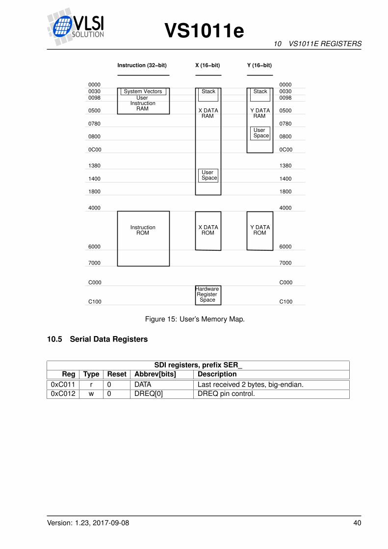
10.3 VS1011e Memory Map
VS1011e’s Memory Map is shown in Figure 15.
10.4 SCI Registers
SCI registers described in Chapter 8.6 can be found here between 0xC000..0xC00F. In additionto these registers, there is one in address 0xC010, called SPI_CHANGE.
SPI registers, prefix SPI_Reg Type Reset Abbrev[bits] Description
0xC010 r 0 CHANGE[5:0] Last SCI access address.
SPI_CHANGE bitsName Bits DescriptionSPI_CH_WRITE 4 1 if last access was a write cycle.SPI_CH_ADDR 3:0 SPI address of last access.
Version: 1.23, 2017-09-08 39
VS1011e10 VS1011E REGISTERS
00000000
Stack Stack
Instruction (32−bit) Y (16−bit)X (16−bit)
System Vectors
UserSpace
Y DATA ROM
X DATA ROM
4000
6000
4000
6000
7000 7000
Instruction ROM
Hardware Register Space
C000
C100 C100
C000
00980098
1380
UserSpace1400
1380
1400
18001800
UserInstruction RAM X DATA
RAMY DATA RAM
0C00
0800
0780 0780
0800
0C00
0030 0030
0500 0500
Figure 15: User’s Memory Map.
10.5 Serial Data Registers
SDI registers, prefix SER_Reg Type Reset Abbrev[bits] Description
0xC011 r 0 DATA Last received 2 bytes, big-endian.0xC012 w 0 DREQ[0] DREQ pin control.
Version: 1.23, 2017-09-08 40
VS1011e10 VS1011E REGISTERS
10.6 DAC Registers
DAC registers, prefix DAC_Reg Type Reset Abbrev[bits] Description
0xC013 rw 0 FCTLL DAC frequency control, 16 LSbs.0xC014 rw 0 FCTLH[4:0] Clock doubler + DAC frequency control MSbs.0xC015 rw 0 LEFT DAC left channel PCM value.0xC016 rw 0 RIGHT DAC right channel PCM value.
Every fourth clock cycle an internal 26-bit counter is added to by (DAC_FCTLH & 15) × 65536+ DAC_FCTLL. Whenever this counter overflows, values from DAC_LEFT and DAC_RIGHTare read and a DAC interrupt is generated.
If DAC_FCTL[4] is 1, the internal clock doubler is activated.
10.7 GPIO Registers
GPIO registers, prefix GPIO_Reg Type Reset Abbrev[bits] Description
0xC017 rw 0 DDR[3:0] Direction.0xC018 r 0 IDATA[3:0] Values read from the pins.0xC019 rw 0 ODATA[3:0] Values set to the pins.
GPIO_DIR is used to set the direction of the GPIO pins. 1 means output. GPIO_ODATAremembers its values even if a GPIO_DIR bit is set to input.
GPIO registers don’t generate interrupts.
Version: 1.23, 2017-09-08 41
VS1011e10 VS1011E REGISTERS
10.8 Interrupt Registers
Interrupt registers, prefix INT_Reg Type Reset Abbrev[bits] Description
0xC01A rw 0 ENABLE[2:0] Interrupt enable.0xC01B w 0 GLOB_DIS[-] Write to add to interrupt counter.0xC01C w 0 GLOB_ENA[-] Write to subtract from interript counter.0xC01D rw 0 COUNTER[4:0] Interrupt counter.
INT_ENABLE controls the interrupts. The control bits are as follows:
INT_ENABLE bitsName Bits DescriptionINT_EN_SDI 2 Enable Data interrupt.INT_EN_SCI 1 Enable SCI interrupt.INT_EN_DAC 0 Enable DAC interrupt.
Note: It may take up to 6 clock cycles before changing INT_ENABLE has any effect.
Writing any value to INT_GLOB_DIS adds one to the interrupt counter INT_COUNTER andeffectively disables all interrupts. It may take up to 6 clock cycles before writing to this registerhas any effect.
Writing any value to INT_GLOB_ENA subtracts one from the interrupt counter (unless INT_COUNTERalready was 0). If the interrupt counter becomes zero, interrupts selected with INT_ENABLEare restored. An interrupt routine should always write to this register as the last thing it does,because interrupts automatically add one to the interrupt counter, but subtracting it back to itsinitial value is the responsibility of the user. It may take up to 6 clock cycles before writing thisregister has any effect.
By reading INT_COUNTER the user may check if the interrupt counter is correct or not. If theregister is not 0, interrupts are disabled.
Version: 1.23, 2017-09-08 42
VS1011e10 VS1011E REGISTERS
10.9 System Vector Tags
The System Vector Tags are tags that may be replaced by the user to take control over severaldecoder functions.
10.9.1 AudioInt, 0x20
Normally contains the following VS_DSP assembly code:
jmpi DAC_INT_ADDRESS,(i6)+1
The user may, at will, replace the instruction with a jmpi command to gain control over theaudio interrupt.
10.9.2 SciInt, 0x21
Normally contains the following VS_DSP assembly code:
jmpi SCI_INT_ADDRESS,(i6)+1
The user may, at will, replace the instruction with a jmpi command to gain control over the SCIinterrupt.
10.9.3 DataInt, 0x22
Normally contains the following VS_DSP assembly code:
jmpi SDI_INT_ADDRESS,(i6)+1
The user may, at will, replace the instruction with a jmpi command to gain control over the SDIinterrupt.
10.9.4 UserCodec, 0x0
Normally contains the following VS_DSP assembly code:
jrnop
Version: 1.23, 2017-09-08 43
VS1011e10 VS1011E REGISTERS
If the user wants to take control away from the standard decoder, the first instruction should bereplaced with an appropriate j command to user’s own code.
Unless the user is feeding MP3 data at the same time, the system activates the user programin less than 1 ms. After this, the user should steal interrupt vectors from the system, and insertuser programs.
10.10 System Vector Functions
The System Vector Functions are pointers to some functions that the user may call to helpimplementing his own applications.
10.10.1 WriteIRam(), 0x2
VS_DSP C prototype:
void WriteIRam(register __i0 u_int16 *addr, register __a1 u_int16 msW, register __a0 u_int16lsW);
This is the only supported way to write to the User Instruction RAM. This is because InstructionRAM cannot be written when program control is in RAM. Thus, the actual implementation ofthis function is in ROM, and here is simply a tag to that routine.
10.10.2 ReadIRam(), 0x4
VS_DSP C prototype:
u_int32 ReadIRam(register __i0 u_int16 *addr);
This is the only supported way to read from the User Instruction RAM. This is because Instruc-tion RAM cannot be read when program control is in RAM. Thus, the actual implementation ofthis function is in ROM, and here is simply a tag to that routine.
A1 contains the MSBs and a0 the LSBs of the result.
10.10.3 DataBytes(), 0x6
VS_DSP C prototype:
Version: 1.23, 2017-09-08 44
VS1011e10 VS1011E REGISTERS
u_int16 DataBytes(void);
If the user has taken over the normal operation of the system by switching the pointer in User-Codec to point to his own code, he may read data from the Data Interface through this and thefollowing two functions.
This function returns the number of data bytes that can be read.
10.10.4 GetDataByte(), 0x8
VS_DSP C prototype:
u_int16 GetDataByte(void);
Reads and returns one data byte from the Data Interface. This function will wait until there isenough data in the input buffer.
10.10.5 GetDataWords(), 0xa
VS_DSP C prototype:
void GetDataWords(register __i0 __y u_int16 *d, register __a0 u_int16 n);
Read n data byte pairs and copy them in big-endian format (first byte to MSBs) to d. Thisfunction will wait until there is enough data in the input buffer.
Version: 1.23, 2017-09-08 45
VS1011e11 VS1011 VERSION CHANGES
11 VS1011 Version Changes
This chapter describes changes between different generations of VS1011.
11.1 Changes Between VS1011b and VS1011e, 2005-07-13
• Faster decoding: all codecs, bitrates and bass + treble controls can be used at CLKI = 24MHz.
• Register SCI_BASS now also has a treble control (Chapter 8.6.3). Loudness plugin notrequired.
• Can play IMA ADPCM in mono and stereo (Chapter 8.2.4).
• Register space can now be written to with SCI_WRAM (Chapter 8.6.7).
• Memory and register space can now be read from with SCI_WRAM (Chapter 8.6.7).
• Added optional playback of MPEG 1 and 2 layers I and II (MP1 and MP2) (Chapters 8.2.2,8.2.1 and 8.6.1).
• SPI Boot added (Chapter 9.4).
• MPEG 1, 2 and 2.5 layer III (MP3) decoding more robust against bit errors.
• MPEG 2.5 decoding compatibility enhanced.
• DREQ goes down during SCI operations. (Chapter 7.4).
• DREQ goes down during memory test. (Chapter 7.4).
• In VS1011e the SS_VER field in SCI_STATUS is 2.
• Also SOIC-28 is now a lead-free RoHS-compliant package.
11.2 Migration Checklist from VS1011b to VS1011e, 2005-07-13
• The SS_VER field in SCI_STATUS is 2. You can use SCI_STATUS and SCI_MODE todistinguish between VS1002 and VS1011e. VS1011b has SS_VER=1, SM_SDINEW=0,VS1011e has SS_VER=2, SM_SDINEW=0, and VS1002 has SS_VER=2, SM_SDINEW=1.
• Use built-in bass enhancer and treble control instead of the Loudness plugin. The loud-ness plugin works, but the builtin controls are much faster.
Version: 1.23, 2017-09-08 46
VS1011e12 DOCUMENT VERSION CHANGES
12 Document Version Changes
This chapter describes the latest and most important changes to this document.
Version 1.23, 2017-09-08
• Removed MP2 and MP3 license descriptions from Chapter 1, Licenses, and other rele-vant places, as all their patents have expired.
• Removed mentions of BGA-49 package.
• Other minor updates.
Version 1.22, 2014-12-19
• Updated telephone number in Chapter 13, Contact Information.
Version 1.21 for VS1011e, 2014-12-08
Updated Figure 4, Typical Connection Diagram Using LQFP-48.
Version 1.20 for VS1011e, 2014-02-25
Specification change affected recommended operating conditions if clock doubler is used inChapter 4.2, Recommended Operating Conditions.
Version 1.10 for VS1011e, 2012-02-29
• SCI Test description fixed in Chapter 9.7.4.
• Connection diagram in Chapter 6 updated for improved ESD protection (20Ω GBUF re-sistor replaced with 10Ω).
• Simplified drawing of LQFP48 package dimensions added to Chapter 5.1.1.
• Added SPI timing diagram to Chapter 7.2.1 for newmode SDI.
Version 1.05 for VS1011e, 2009-10-06
• SPI timing clarification (CLKI vs. XTALI) in section 7.6.
• Added CLOCKF example for 12.288 MHz clock to section 8.6.4.
Version: 1.23, 2017-09-08 47
VS1011e12 DOCUMENT VERSION CHANGES
Version 1.04 for VS1011e, 2007-10-08
• Starting from VS1011e also SOIC-28 is a RoHS-compliant lead-free package.
Version: 1.23, 2017-09-08 48
VS1011e13 CONTACT INFORMATION
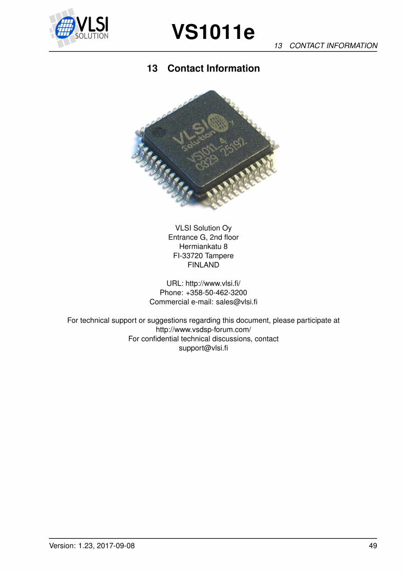
13 Contact Information
VLSI Solution OyEntrance G, 2nd floor
Hermiankatu 8FI-33720 Tampere
FINLAND
URL: http://www.vlsi.fi/Phone: +358-50-462-3200
Commercial e-mail: [email protected]
For technical support or suggestions regarding this document, please participate athttp://www.vsdsp-forum.com/
For confidential technical discussions, [email protected]
Version: 1.23, 2017-09-08 49