volume iii, issue v, may 2014 ijltemas issn 2278 - 2540 ... · designing of modified sepic...
TRANSCRIPT
Volume III, Issue V, May 2014 IJLTEMAS ISSN 2278 - 2540
www.ijltemas.in Page 234
Designing of Modified SEPIC Converter for LED
Lamp Driver
Vineet Sharma
Urooj Sultana Uttam Kumar Gupta
Electrical Engineering Electronics Engineering Electrical Engineering
DKNMU Newai, Rajasthan AIT Tonk,Rajasthan DKNMU Newai, Rajasthan
Newai, India 304021 Tonk, India 304021 Newai, India 304021
[email protected] [email protected] [email protected]
Abstract:-Due to the recent advancement in the Light
Emitting Diode (LED) technology, high brightness white
LED becomes feasible in residential, industry and
commercial applications to replace the incandescent bulbs,
halogen bulbs, and even compact fluorescent light bulbs. In
these offline applications, high power factor, and low
harmonics are of primary importance.
In this paper, we proposed a high power factor SEPIC
converter for the high brightness. The harmonics of the
input line current is reduced and power factor is high.
A current feedback loop is proposed to control the LED
brightness. This circuit has the advantages of one stage of
power conversion, no need to sense the input voltage, simple
feedback control, and voltage step-up and down, high power
factor and dimmable LED current.
LEDs plays a vital role in the industry and in our life. The
SEPIC converter is to increase the efficiency of LEDs and
get the better resolution than the other lighting application.
Keywords—harmonics, SEPIC, feedbackloop, conversion,
resolution.
I. INTRODUCTION
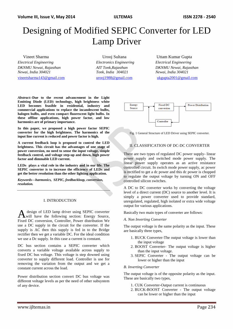
design of LED lamp driver using SEPIC converter
will have the following section: Energy Source,
Fixed DC conversion, Controller, Power distribution We
use a DC supply in the circuit for the converter. If the
supply is AC then this supply is fed in to the Bridge
rectifier then we get a variable DC. For the ideal condition
we use a Dc supply. In this case a current is constant.
DC bus section contains a SEPIC converter which
converts a variable voltage available across supply to
fixed DC bus voltage. This voltage is step downed using
converter to supply different load. Controller is use for
removing the variation from the output and we get a
constant current across the load.
Power distribution section convert DC bus voltage was
different voltage levels as per the need of other subsystem
of any device.
Fig. 1 General Structure of LED Driver using SEPIC converter.
II. CLASSIFICATION OF DC-DC CONVERTER
There are two types of regulated DC power supply- linear
power supply and switched mode power supply. The
linear power supply operates as an active resistance
controlled circuit. In switch mode power supply, ac power
is rectified to get a dc power and this dc power is chopped
to regulate the output voltage by turning ON and OFF
controlled silicon switches.
A DC to DC converter works by converting the voltage
level of a direct current (DC) source to another level. It is
simply a power converter used to provide standard,
unregulated, regulated, high isolated or extra wide voltage
output for various applications.
Basically two main types of converter are follows:
A. Non Inverting Converter
The output voltage is the same polarity as the input. These
are basically three types,
1. BUCK Converter-The output voltage is lower than
the input voltage
2. BOOST Converter- The output voltage is higher
than the input voltage.
3. SEPIC Converter - The output voltage can be
lower or higher than the input
B. Inverting Converter
The output voltage is of the opposite polarity as the input.
These are basically two types,
1. CUK Converter-Output current is continuous
2. BUCK-BOOST Converter - The output voltage
can be lower or higher than the input
A
Volume III, Issue V, May 2014 IJLTEMAS ISSN 2278 - 2540
www.ijltemas.in Page 235
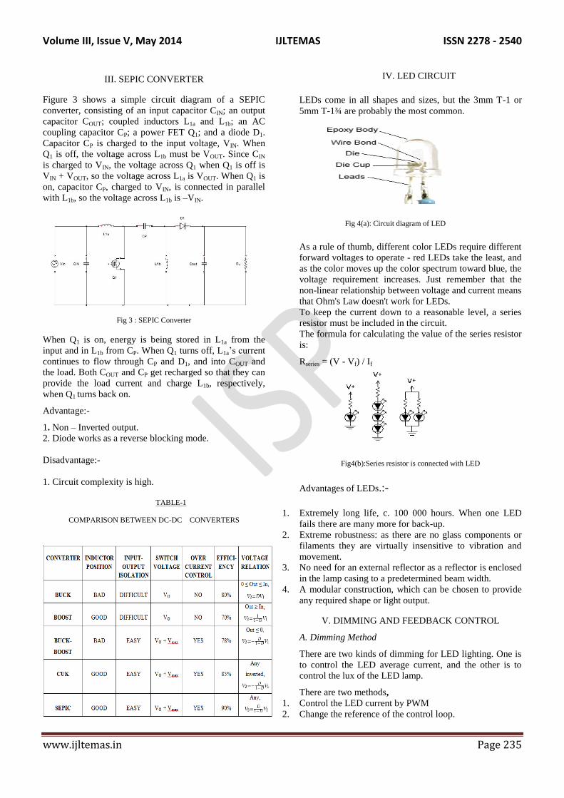
III. SEPIC CONVERTER
Figure 3 shows a simple circuit diagram of a SEPIC
converter, consisting of an input capacitor CIN; an output
capacitor COUT; coupled inductors L1a and L1b; an AC
coupling capacitor CP; a power FET Q1; and a diode D1.
Capacitor CP is charged to the input voltage, VIN. When
Q1 is off, the voltage across L1b must be VOUT. Since CIN
is charged to VIN, the voltage across Q1 when Q1 is off is
VIN + VOUT, so the voltage across L1a is VOUT. When Q1 is
on, capacitor CP, charged to VIN, is connected in parallel
with L1b, so the voltage across L1b is –VIN.
Fig 3 : SEPIC Converter
When Q1 is on, energy is being stored in L1a from the
input and in L1b from CP. When Q1 turns off, L1a’s current
continues to flow through CP and D1, and into COUT and
the load. Both COUT and CP get recharged so that they can
provide the load current and charge L1b, respectively,
when Q1 turns back on.
Advantage:-
1. Non – Inverted output.
2. Diode works as a reverse blocking mode.
Disadvantage:-
1. Circuit complexity is high.
TABLE-1
COMPARISON BETWEEN DC-DC CONVERTERS
IV. LED CIRCUIT
LEDs come in all shapes and sizes, but the 3mm T-1 or
5mm T-1¾ are probably the most common.
Fig 4(a): Circuit diagram of LED
As a rule of thumb, different color LEDs require different
forward voltages to operate - red LEDs take the least, and
as the color moves up the color spectrum toward blue, the
voltage requirement increases. Just remember that the
non-linear relationship between voltage and current means
that Ohm's Law doesn't work for LEDs.
To keep the current down to a reasonable level, a series
resistor must be included in the circuit.
The formula for calculating the value of the series resistor
is:
Rseries = (V - Vf) / If
Fig4(b):Series resistor is connected with LED
Advantages of LEDs.:-
1. Extremely long life, c. 100 000 hours. When one LED
fails there are many more for back-up.
2. Extreme robustness: as there are no glass components or
filaments they are virtually insensitive to vibration and
movement.
3. No need for an external reflector as a reflector is enclosed
in the lamp casing to a predetermined beam width.
4. A modular construction, which can be chosen to provide
any required shape or light output.
V. DIMMING AND FEEDBACK CONTROL
A. Dimming Method
There are two kinds of dimming for LED lighting. One is
to control the LED average current, and the other is to
control the lux of the LED lamp.
There are two methods,
1. Control the LED current by PWM
2. Change the reference of the control loop.
Volume III, Issue V, May 2014 IJLTEMAS ISSN 2278 - 2540
www.ijltemas.in Page 236
1). Control the LED current by PWM
In the PWM method, the LED current is controlled by a
small power MOSFET, the duty ratio D of which varies
for dimming. In dimming circuits, a low power MOSFET
is connected in series with the LED string. The MOSFET
is controlled by the PWM of the dimming frequency fd.
At D/fd, the LED conducts a constant current Io. So the
tune of the color does not change with the brightness. At
(1-D)/fd, LED current is turned off. The LED can be
turned on and off very fast without any negative effect.
The average of the LED current is DIo. Hence brightness
is changed with D. This method is widely used in display
applications.
2.Change the reference of the control loop.
The other is the so-called analog control, that is, to control
the reference of the loop. By changes the reference signal,
the LED current can be adjusted. In return, the brightness
of LED is changed. Based on how the reference signal is
adjusted, there are further two methods.
i. DC dimming method
ii. AC dimming method
i) DC Dimming Method.
In A DC Dimming Method, The Reference Is Obtained
From A Constant 5V Source And Is Changed Using A
Variable Resistor Or Digital Controlled Resistor.
ii) AC Dimming Method.
In This Method, The Reference Is In Proportion To The
Input Ac Average Voltage. Therefore, The Widely Used
Traditional Dimmer Can Be Used In Combination To
Adjust The LED Current. Both Of These Methods
Regulate The LED Current To Adjust The LED
Brightness.
VI. MODELING OF CONVERTER
Voltage across the LEDs varies depending upon the
isolation, temperature at which they are operating. This
voltage can vary over a wide range, we may need to step
up or step down the voltage. This can be done using either
BUCK-BOOST converter or SEPIC converter. SEPIC
converter is chosen because its output voltage is of same
sign as that of input. Connection diagram of system is as
shown in Fig 6.
Fig 6: Block Diagram of the System.
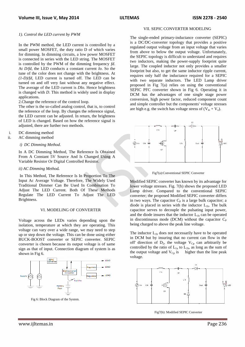
VII. SEPIC CONVERTER MODELING
The single-ended primary-inductance converter (SEPIC)
is a DC/DC-converter topology that provides a positive
regulated output voltage from an input voltage that varies
from above to below the output voltage. Unfortunately,
the SEPIC topology is difficult to understand and requires
two inductors, making the power-supply footprint quite
large. The coupled inductor not only provides a smaller
footprint but also, to get the same inductor ripple current,
requires only half the inductance required for a SEPIC
with two separate inductors. The LED Lamp driver
proposed in Fig 7(a) relies on using the conventional
SEPIC PFC converter shown in Fig 6. Operating it in
DCM has the advantages of one single stage power
conversion, high power factor, reduced component count
and simple controller but the components' voltage stresses
are high e.g. the switch has voltage stress of (Vin + Vo).
Fig7(a):Conventional SEPIC Converter
Modified SEPIC converter has known by its advantage for
lower voltage stresses. Fig. 7(b) shows the proposed LED
Lamp driver. Compared to the conventional SEPIC
converter; the proposed Modified SEPIC converter differs
in two ways. The capacitor CP is a large bulk capacitor; a
diode is placed in series with the inductor L1b. The bulk
capacitor serves to decouple the pulsating input power,
and the diode insures that the inductor L1b can be operated
in discontinuous mode (DCM) without the capacitor CP
being charged to above the peak line voltage.
The inductor L1b does not necessarily have to be operated
in DCM but by insuring that no current can flow in the
off' direction of D2, the voltage VCp can arbitrarily be
controlled by the ratio of L1a to L1b, as long as the sum of
the output voltage and VCp is higher than the line peak
voltage.
Fig7(b): Modified SEPIC Converter
Volume III, Issue V, May 2014 IJLTEMAS ISSN 2278 - 2540
www.ijltemas.in Page 237
Fig 7(c):SEPIC Component current during CCM
VIII. PRINCIPAL OF OPERATION AND ANALYSIS
Figure7(a) shows a simple circuit diagram of a Modified
SEPIC converter, consisting of an input capacitor CIN; an
output capacitor COUT; coupled inductors L1a and L1b; an
AC coupling capacitor CP; a power FET Q1 and a diode
D1. Capacitor CP is charged to the input voltage VIN.
Knowing this, we can easily determine the voltages as
shown in Fig7(c). When Q1 is off, the voltage across L1b
must be VOUT. Since CIN is charged to VIN, the voltage
across Q1 when Q1 is off is VIN + VOUT, so the voltage
across L1a is VOUT. When Q1 is on, capacitor CP, charged
to VIN, is connected in parallel with L1b, so the voltage
across L1b is –VIN. The currents flowing through various
circuit components are shown in Fig7(c)
Fig 8(a): CCM during when Q1 is on
When Q1 is on, energy is being stored in L1a from the
input and in L1b from CP. When Q1 turns off, L1a current
continues to flow through CP and D1, and into COUT and
the load. Both COUT and CP get recharged so that they can
provide the load current and charge L1b, respectively,
when Q1 turns back on.
Fig 8(b) :CCM during when Q1 is off.
IX. DESIGN OF PASSIVE COMPONENTS
A. Specification o f System
Input Voltage Vg = 140 V
Output Voltage Vo = 120 V
Switching Frequency fs = 75 kHz
Switching Period Ts = 13.3 µ sec
Maximum Inductor Current = 1.5 A
B. Design of Input Inductor (L1)
From system specifications and circuit parameters
inductance value is calculated using the following
equation.
L1 =
The inductance value was found as 160 µH.
C. Design of Output Inductor (L2)
For this inductor peak to peak ripple current is fixed to 5%
of inductor current.
L1 =
Following same steps for this inductor as that of above
inductor and using the above equation yields value of this
inductance as 80 µH.
D. Design of Capacitor, C1
This capacitor is designed by fixing the voltage ripple to
10%.Value of capacitance can be calculated as follows,
C1 = (2.8)
Capacitance value was found to be 180 µF.
E. Design of Output Capacitor, C2
Output capacitor is designed to filter out the ripple in load
current. capacitance can be calculated as follows
Volume III, Issue V, May 2014 IJLTEMAS ISSN 2278 - 2540
www.ijltemas.in Page 238
C2 =
Peak to peak ripple was fixed to 6% and substituting all
other values as per system specifications capacitance
value was found to be 82 µF.
X. CONTROLLER DESIGN CURRENT
PROGRAMMED MODE CONTROL
Analog Current programmed mode control involves
controlling of converter output voltage either by
controlling peak or valley current of switch or inductor. It
is called peak current mode control when maximum
current of switch or inductor is compared with reference.
Output voltage of converter is continuously compared
with reference voltage. Error obtained after comparison is
fed to the controller, which generates a current reference
iref .Whenever the switch is turned on inductor current
starts increasing. This inductor current is continuously
compared with reference generated by the controller.
Switch is turned off for later part of switching interval
when inductor current exceeds the reference. During turn
off inductor current starts decreasing. Inductor current
starts increasing when switch is turned on in next
switching interval.
Fig 9: Schematic diagram of converter incorporating current mode
control.
XI. DESIGN OF CONTROLLER:
As input voltage of the converter varies but we have to
keep the output voltage at a constant value. So an
appropriate controller is required to do this job. This
controller will generate current reference for inner
predictive loop; with the help of this current reference
duty cycle for next switching cycle will be generated.
Block diagram of this whole scheme is shown in Fig12.
Figure 12 : Control structure
The transfer function of the system is:
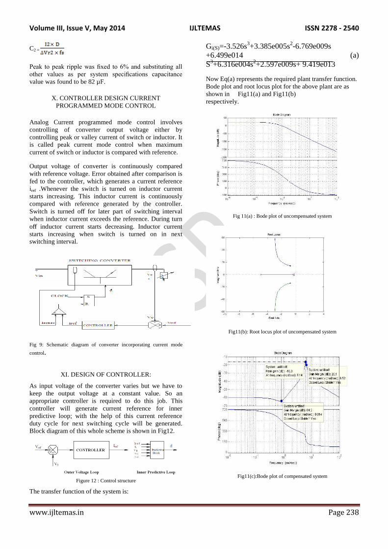
Gi(S)=-3.526s3+3.385e005s
2-6.769e009s
+6.499e014 (a)
S3+6.316e004s
2+2.597e009s+ 9.419e013
Now Eq(a) represents the required plant transfer function.
Bode plot and root locus plot for the above plant are as
shown in Fig11(a) and Fig11(b)
respectively.
Fig 11(a) : Bode plot of uncompensated system
Fig11(b): Root locus plot of uncompensated system
Fig11(c):Bode plot of compensated system
Volume III, Issue V, May 2014 IJLTEMAS ISSN 2278 - 2540
www.ijltemas.in Page 239
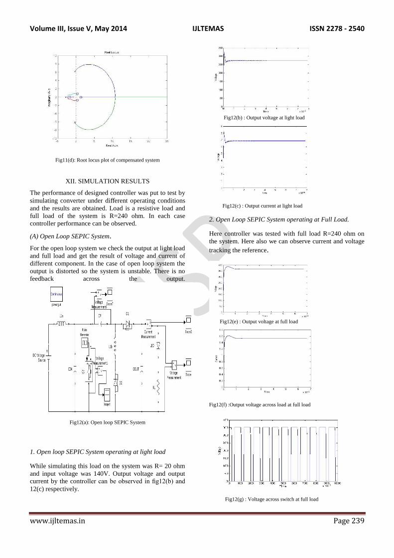
Fig11(d): Root locus plot of compensated system
XII. SIMULATION RESULTS
The performance of designed controller was put to test by
simulating converter under different operating conditions
and the results are obtained. Load is a resistive load and
full load of the system is R=240 ohm. In each case
controller performance can be observed.
(A) Open Loop SEPIC System.
For the open loop system we check the output at light load
and full load and get the result of voltage and current of
different component. In the case of open loop system the
output is distorted so the system is unstable. There is no
feedback across the output.
Fig12(a): Open loop SEPIC System
1. Open loop SEPIC System operating at light load
While simulating this load on the system was R= 20 ohm
and input voltage was 140V. Output voltage and output
current by the controller can be observed in fig12(b) and
12(c) respectively.
Fig12(b) : Output voltage at light load
Fig12(c) : Output current at light load
2. Open Loop SEPIC System operating at Full Load.
Here controller was tested with full load R=240 ohm on
the system. Here also we can observe current and voltage
tracking the reference.
Fig12(e) : Output voltage at full load
Fig12(f) :Output voltage across load at full load
Fig12(g) : Voltage across switch at full load

Volume III, Issue V, May 2014 IJLTEMAS ISSN 2278 - 2540
www.ijltemas.in Page 240
Fig12(h): Capacitor voltage across Cout at full load
(A) Closed Loop SEPIC System.
For the closed loop system we check the output at light
load and full load and get the result of voltage and current
of different component. In the case of closed loop system
the output is controllable so the system is stable. There is
feedback across the output. Closed loop SEPIC system
shown in Fig12(j).
1. Closed loop SEPIC system at light load
Closed loop results of SEPIC converter at light load
circuit were presented here. While taking these readings
input voltage was kept at 140V and period of switching
was 13.3µ sec. Light load R=20 ohm.
Fig12(i): Output voltage across load at light
load.
Fig12(j):Closed loop SEPIC system
Fig12(k) : Output current across the load at light load
Fig12(l): Voltage across Cp at light load
2 .Closed loop SEPIC system at full load.
Closed loop system of SEPIC system shown in Fig 4.11.
Result of voltage and current of different component at
full load R=240 ohm shown below.
Fig12(m) : Output voltage across load at full load
Fig12(n):Output current across load at full load

Volume III, Issue V, May 2014 IJLTEMAS ISSN 2278 - 2540
www.ijltemas.in Page 241
Fig12(o) : voltage across switch at full load
Fig12(p):Voltage across Cp at full load
Fig12(q) : MOSFET gate signal
CONCLUSIONS
This paper addresses design and implementation of peak
current mode controlled SEPIC converter that can be used
in low power applications.
General structure of LED lamp driver system was
explained and a suitable power supply structure was
proposed for lighting applications. SEPIC converter was
chosen to generate a fixed DC voltage from variable DC
available at supply.
Modelling of SEPIC converter under perturbed conditions
was done using state space averaging approach. Passive
components required for SEPIC converter are designed.
SEPIC converter is a 4th order system so predictive peak
current mode control was chosen because it offers simple
dynamics and inherent peak current protection. Developed
mathematical along with designed controller is simulated
using MATLAB/Simulink.Controller performance was
checked for different operating conditions. In each case it
was observed that both output voltage and inductor
current are tracking their references.
REFERENCES
[1] Soo-Seok Kim, Seung-Pil Mun, “A New Sepic- Flyback
Converter” IEEE lnduslrial Electronics Soclety, November 2 - 6, 2004, Busan, Korea.
[2] Pan TianFu, Chiu HuangJen, Cheng ShihJen, Chyng
ShihYen, “An Improved Single - Stage Flyback PFC Converter for High-Luminance Lighting LED Lamps,"
Electronic Measurement and Instruments, pp. 4-212 - 4- 215,
Aug. 16 2007.
[3] Zhongming Ye, Greenfeld, F., Zhixiang Liang, “Offline SEPIC converter to drive the high brightness white LED for
lighting applications", Industrial Electronics, pp. 1994 -
2000, Nov 2008.
[4] Shen, C.-L., Wu, Y.-E., Chen, M.-H., “A modified SEPIC converter with soft-switching feature for power factor
correction," Industrial Technology pp. 1 - 6, April 2008.
[5] Zhongming Ye, Fred Greenfeld, and Zhixiang Liang,
“Single-Stage Offline SEPIC Converter with Power Factor
Correction to Drive High Brightness LEDs” 2009.
[6] Diego Gonz´alez Lamar, Diego Gonz´alez Lamar, “A Very
Simple Control Strategy or Power Factor Correctors Driving High-Brightness LEDs” IEEE Transactions On Power
Electronics, Vol. 24, No. 8, August 2009 .
[7] Ying-Chun Chuang, Yu-Lung Ke “Single-Stage Power-
Factor-Correction Circuit with Flyback Converter to Drive LEDs for Lighting Applications” IEEE 2010.
[8] Petersen, L, “Input-current-shaper based on a modified
SEPIC converter with low voltage stress," Power Electronics Specialists Conference pp. 666-671 vol.2, June 2001.