voltage regulators - aeroflexams.aeroflex.com/pagesproduct/datasheets/vrg/vrg_ecatalog.pdf ·...
TRANSCRIPT

A passion for performance.
Voltage Regulators
From Aeroflex Plainview
HiRel Off-the-Shelf Products
Radiation HardnessAssurance Plan DLA Certified toMIL-PRF-38534,Appendix G
January 2012

ADJUSTABLE VOLTAGE REGULATORS SELECTION GUIDE
Click on Part Number for Detailed Data Sheet
Click on Drawing Number to View DSCC SMD
Click on Package Style for Detailed Mechanical Drawing
6-PinTO-257
PART NUMBER Su
rface Mount
# Leads
SMD
Part Nu
mber
Positive
Voltage
Range (V)
Total # Regula
tors
Thru-Hole
Positive
Output
Current (A
)
# Positive
Regulators
Package Style
Package Size
L x W x H
(inches)
Total D
ose krads(S
i)
# Ne
gative
Regulators
Negative Voltage
Range (V)
VRG8601 2 1 1.2 to 37 1 -1.2 to -27 1.5 1.5 100 TO-257 0.65x0.42x0.220 6 5962-0521901KXX
VRG8602 2 1 1.2 to 37 1 -1.2 to -27 1.5 1.5 100 TO-257 0.65x0.42x0.220 6 5962-0521901KYX
VRG8607 2 2 1.2 to 37 1.5 1.5 100 TO-257 0.65x0.42x0.220 6 5962-0521903KXX
VRG8608 2 2 1.2 to 37 1.5 1.5 100 TO-257 0.65x0.42x 0.220 6 5962-0521903KYX
VRG8609 2 2 -1.2 to -27 1.5 1.5 100 TO-257 0.65x0.42x0.220 6 5962-0521904KXX
VRG8610 2 2 -1.2 to -27 1.5 1.5 100 TO-257 0.65x0.42x 0.220 6 5962-0521904KYX
VRG8651 2 1.30 1 1.3 to 23 1 -2.5 to -25 1.0 3.0 100 TO-257 0.75x0.42x0.220 8 5962-0920101KUX
VRG8652 2 1.30 1 1.3 to 23 1 -2.5 to -25 1.0 3.0 100 TO-257 0.75x0.42x0.220 8 5962-0920101KZX
VRG8653 2 1.60 1 1.3 to 30 1 -2.5 to -25 3.0 3.0 100 TO-257 0.75x0.42x0.220 8 5962-1021301KUX
VRG8654 2 1.60 1 1.3 to 30 1 -2.5 to -25 3.0 3.0 100 TO-257 0.75x0.42x0.220 8 5962-1021301KZX
VRG8657 2 1.30 2 1.3 to 23 1.0 100 TO-257 0.65x0.42x0.220 6 5962-0920102KXX
VRG8658 2 1.30 2 1.3 to 23 1.0 100 TO-257 0.65x0.42x0.220 6 5962-0920102KYX
VRG8660 1 1 1.2 to 37 1.5 100 SMD-0.5 0.40x0.30x0.130 3 5962-0920601KXX
VRG8661 1 1 -1.2 to -27 1.5 100 SMD-0.5 0.40x0.30x0.130 3 5962-0920602KXX
VRG8662 1 1.30 1 1.3 to 23 1.0 100 SMD-0.5 0.40x0.30x0.130 3 5962-0920701KXX
VRG8663 1 1.05 1 -2.5 to -25 3.0 100 SMD 0.55x0.30x0.130 5 5962-0920702KYX
VRG8666 1 0.50 1 0.1 to 34 1.0 100 SMD 0.55x0.30x0.130 5 5962-1120502KYX
VRG8684 1 1.60 1 1.3 to 30 3.0 100 SMD-0.5 0.40x0.30x0.130 3 5962-0924501KXX
VRG8687 2 1.60 2 1.3 to 30 3.0 100 TO-257 0.75x0.42x0.220 8 5962-1021302KUX
VRG8688 2 1.60 2 1.3 to 30 3.0 100 TO-257 0.75x0.42x0.220 8 5962-1021302KZX
VRG8691 1 0.50 1 1.0 to 3.3 7.5 100 Power 0.90x1.00x0.220 12 5962-0923701KXX
VRG8692 1 0.50 1 1.0 to 3.3 7.5 100 Power 0.90x1.00x0.220 12 5962-0923701KYX
Negative Ou
tput
Current (A
)
LDO Regulator
Dropout Voltage
8-PinTO-257
12-PinHermetic
5-PadSMD
3-PadSMD-0.5
Aeroflex Plainview’s Radiation Hardness Assurance Plan is DLA Certified to MIL-PRF-38534, Appendix G

SCD8601 Rev T
DESCRIPTIONThe Aeroflex Plainview VGR8601/02 consists of a positive (RH117) and a negative (RH137) voltage regulator eachcapable of supplying in excess of 1.5Amps over the output voltage range as defined under recommended operatingconditions. Each regulator is exceptionally easy to set-up, requiring only 2 external resistors to set the output voltage.The module design has been optimized for excellent regulation and low thermal transients. There is full electricalisolation between positive and negative regulators and each regulator to the package.Further, the VRG8601/ 02 features internal current limiting, thermal shutdown and safe-area compensation, makingthem virtually blowout-proof against overloads. The VRG8601/02 serves a wide variety of applications includinglocal on-card regulation, programmable output voltage regulation or precision current regulation.The VRG8601/02 has been specifically designed to meet exposure to radiation environments. The VRG8601 isconfigured for a Thru-Hole 6 lead metal power package and the VRG8602 is configured for a Surface Mount 6 leadmetal power package. It is guaranteed operational from -55°C to +125°C. Available screened to MIL-STD-883, theVRG8601/ 02 is ideal for demanding military and space applications. For detailed performance characteristic curves, applications information and typical applications see thelatest Linear Technology Corporation ® data sheets for their RH/LT117 and RH/LT137, which is availableon-line at www.linear.com.
5
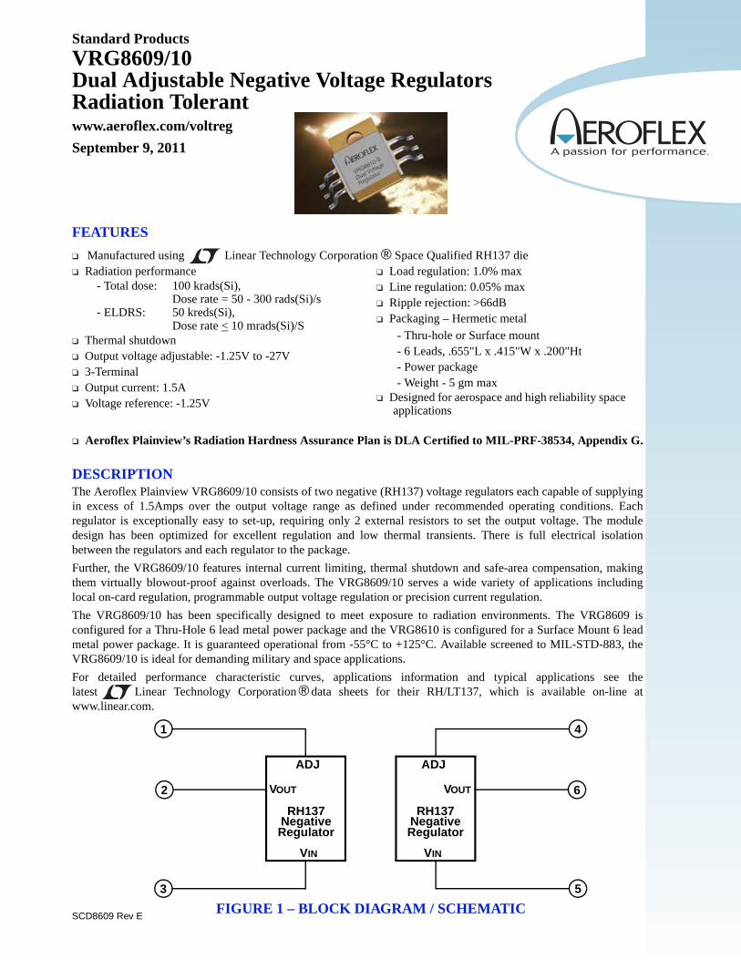
VIN
ADJ
VOUT
RH137
4
3
VIN
ADJ
VOUT
RH117
1
FIGURE 1 – BLOCK DIAGRAM / SCHEMATIC
2 6
PositiveRegulator Regulator
Negative
VRG8601/02
Radiation Tolerant
September 9, 2011
www.aeroflex.com/voltreg
Standard Products
Dual Adjustable Positive/Negative Voltage Regulators
FEATURES Manufactured using Linear Technology Corporation ® Space Qualified RH117 and RH137 die Radiation performance
- Total dose: 100 krads(Si), Dose rate = 50 - 300 rads(Si)/s
- ELDRS: 50 krads(Si), Dose rate < 10 mrads(Si)/s
Two-Independent voltage regulators Thermal shutdown 1.5A output current Adjustable Output Voltages Packaging – Hermetic metal
– Thru-hole or Surface mount– 6 Leads, .655"L x .415"W x .200"Ht– Power package– Weight - 5 gm max
Positive regulator features (RH117)– Output voltage adjustable: +1.25V to 37V– 3-Terminal – Voltage reference: 1.25V– Load regulation: 1.9% max– Line regulation: 0.06% max– Ripple rejection: >66dB
Negative regulator features (RH137)– Output voltage adjustable: -1.25V to -27V– 3-Terminal – Voltage reference: 1.25V– Load regulation: 1.0% typ– Line regulation: .05% typ– Ripple rejection: >66dB
Designed for aerospace and high reliability space applications
Aeroflex Plainview’s Radiation Hardness Assurance Plan is DLA Certified to MIL-PRF-38534, Appendix G.

2SCD8601 Rev T 9/9/11 Aeroflex Plainview
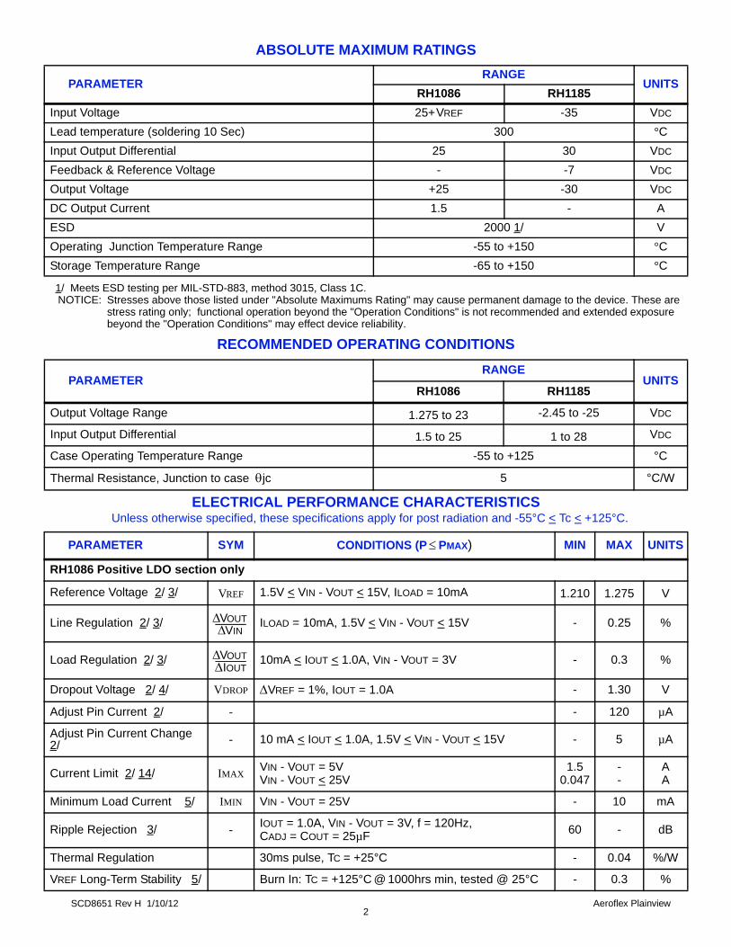
ABSOLUTE MAXIMUM RATINGS
PARAMETER RANGE UNITS
Operating (Junction) Temperature Range -55 to +150 C
Lead Temperature (soldering, 10 sec) 300 °C
Storage Temperature Range -65 to +150 C
Input-Output Voltage Differential 40 (Pos) 30 (Neg) V
Thermal Resistance (junction to case JC) each, Pos. & Neg. 5 °C/W
ESD Rating 1.999 1/ KV
1/ Meets ESD testing per MIL-STD-883, method 3015, Class 1C.
NOTICE: Stresses above those listed under "Absolute Maximums Rating" may cause permanent damage to the device. These are stress rating only; functional operation beyond the "Operation Conditions" is not recommended and extended exposure beyond the "Operation Conditions" may effect device reliability..
RECOMMENDED OPERATING CONDITIONS
PARAMETER RANGE UNITS
Output Voltage Range
Positive Voltage Regulator 1.3 to 37 VDC
Negative Voltage Regulator -1.3 to -27 VDC
Case Operating Temperature Range -55 to +125 °C
POSITIVE REGULATOR – ELECTRICAL PERFORMANCE CHARACTERISTICS 1/
PARAMETER SYM CONDITIONS (P PMAX MIN MAX UNITS
Reference Voltage 4/ VREF 3V < (VIN - VOUT) < VDIFF MAX, 10mA < IOUT < IMAX 1.20 1.30 V
Line Regulation 2/ 4/ 3V < (VIN - VOUT) < VDIFF MAX, IOUT = 10mA - 0.03 %/V
Load Regulation 2/ 4/ 10mA < IOUT < IMAX, VOUT < 5V10mA < IOUT < IMAX, VOUT > 5V
--
601.2
mV%
Thermal RegulationIOUT = 1.5A, (VIN - VOUT) = 13.3V, 20ms Pulse, 20W, TC = +25°C - 0.07 %/W
Ripple Rejection Ratio VOUT = 10V, f = 120Hz, CADJ = 10µF 66 - dB
Adjustment Pin Current 4/ IADJ IOUT = 10mA, 3V < (VIN - VOUT) < 40V - 100 µA
Adjustment Pin Current Change 4/ IADJ
10mA < IOUT < IMAX3V < (VIN - VOUT) < 40V
- 5 µA
Minimum Load Current 3/ 4/ IMIN (VIN - VOUT) = 40V - 5 mA
Current Limit 4/ 5/ IMAX(VIN - VOUT) < 15V 1.5 -
A(VIN - VOUT) = 40V, TC = +25°C 0.30 -
Long Term Stability 3/ TC = +125°C - 1 %
Thermal Resistance, each Regulator(Junction to Case) 3/
JC - 5 °C/W
VOUTVIN
VOUTIOUT
VOUTTIME

3SCD8601 Rev T 9/9/11 Aeroflex Plainview
NEGATIVE REGULATOR – ELECTRICAL PERFORMANCE CHARACTERISTICS 1/
PARAMETER SYM CONDITIONS MIN MAX UNITS
Reference Voltage 4/ VREF 3V < (VIN - VOUT) < VDIFF MAX,10mA < IOUT < IMAX -1.200 -1.300 V
Line Regulation 2/ 4/ 3V < (VIN - VOUT) < 30V, - 0.05 %/V
Load Regulation 2/ 4/10mA < IOUT < IMAX, VOUT < 5V - 50 mV
10mA < IOUT < IMAX, VOUT > 5V - 1.0 %
Thermal RegulationIOUT = 1.5A, (VIN - VOUT) = 13.3V, 20ms Pulse, 20W,TC = +25°C - 0.02 %/W
Ripple Rejection VOUT = -10V, f = 120Hz, CADJ = 10µF 66 - dB
Adjustment Pin Current 4/ IADJ IOUT = 10mA, 3V < (VIN - VOUT) < 30V - 100 µA
Adjustment Pin Current Change 4/ IADJ
10mA < IOUT < IMAX3V < (VIN - VOUT) < 30V
- 5 µA
Minimum Load Current 3/ 4/ IMIN(VIN - VOUT) = 30V - 5
mA(VIN - VOUT) < 10V - 3
Current Limit 4/ 5/ IMAX(VIN - VOUT) < 15V 1.5 -
A(VIN - VOUT) = 30V, TC = +25°C 0.24 -
Long Term Stability 3/ TC = +125°C - 1 %
Thermal Resistance, each Regulator (Junction to Case) 3/
JC - 5 °C/W
Notes:1/ Unless otherwise specified, these specifications apply for (Vin - Vout) = 5V, Iout = 0.5A and -55°C < Tc < +125°C.2/ Regulation is measured at a constant junction temperature, using pulse testing with a low duty cycle. Changes in output voltage due to
heating effects are covered under the specification for thermal regulation. Measurements taken at the output lead must be adjusted for lead resistance.
3/ Not tested. Shall be guaranteed to the specified limits. 4/ Specification derated to reflect High Dose Rate (1019 condition A) to 100 krad(Si) and Low Dose Rate (1019 condition D) to 50 krad(Si),
@ +25°C.5/ Pulsed @ < 10% duty cycle @ +25°C.
VOUTVIN
VOUTIOUT
VOUTTIME

4SCD8601 Rev T 9/9/11 Aeroflex Plainview
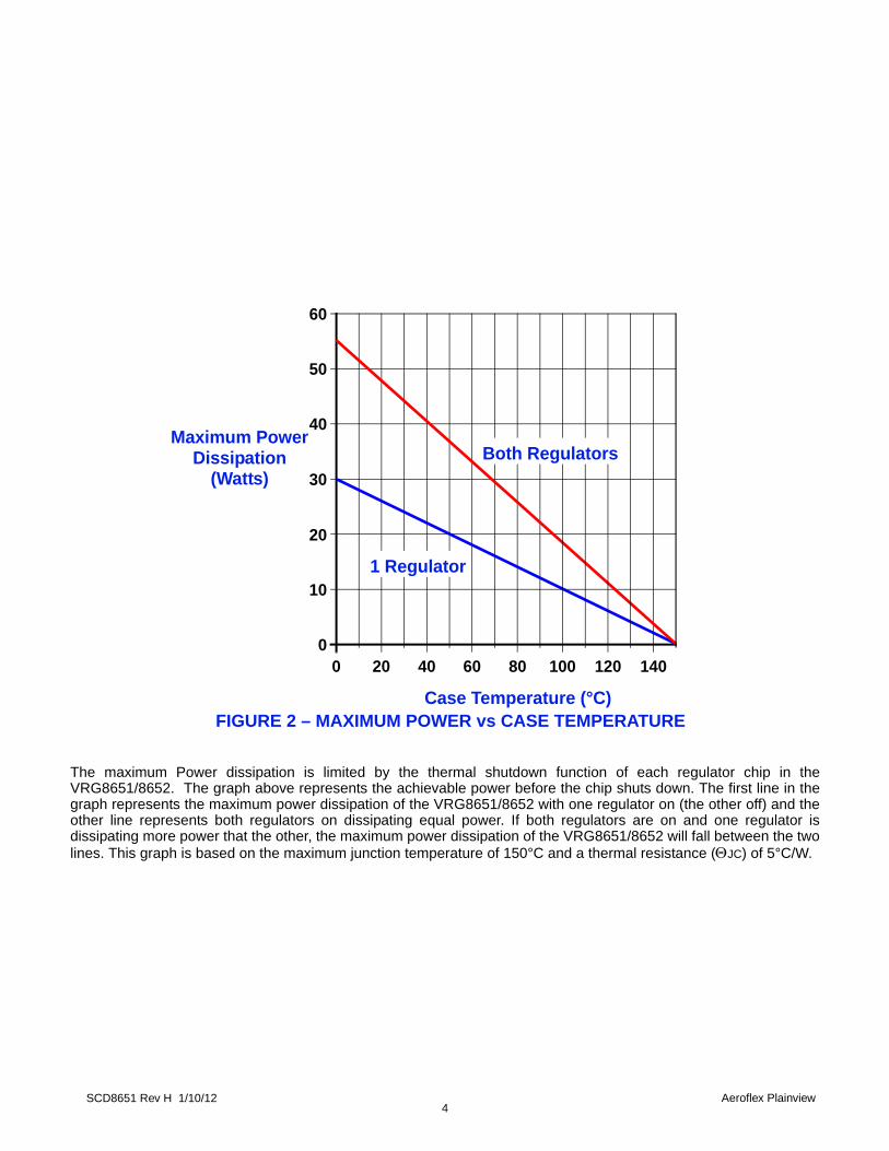
FIGURE 2 – MAXIMUM POWER vs CASE TEMPERATURE
The maximum Power dissipation is limited by the thermal shutdown function of each regulator chip in the VRG8601/02. Thegraph above represents the achievable power before the chip shuts down. The first line in the graph represents the maximumpower dissipation of the VRG8601/02 with one regulator on (the other off) and the other line represents both regulators ondissipating equal power. If both regulators are on and one regulator is dissipating more power that the other, the maximum powerdissipation of the VRG8601/02 will fall between the two lines. This graph is based on the maximum junction temperature of150°C and a thermal resistance (JC) of 5°C/W.
60
50
40
30
20
10
0 20 40 60 80 100 120 140
Case Temperature (°C)
1 Regulator
0
Both RegulatorsMaximum Power
Dissipation(Watts)
IADJ = 50µAVREF = 1.25V,
+Reg = VOUT = VREF (1+R2/R1) + (IADJ x R2)-Reg = VOUT = -VREF (1+R2/R1) + (-IADJ x R2)
VRG8601/02VIN VOUT
ADJ
R1
R2
VREF
Adjustable Regulator
FIGURE 3 – TYPICAL APPLICATIONS

5SCD8601 Rev T 9/9/11 Aeroflex Plainview
.108
.200
.100
.123
ø.145 THRU
.415.2075
R.065 TYP.4 PLCS
.655
.415 SQ
±.003
.220 MAX.
±.005
.040
±.002.030 DIA.
.150 REF. 2° MAX. TYP.
±.020.720MEASURED
LEAD TIP
IDENTESD/PIN 1
–B–
–A–
–C–
ø.010 B C A
Mø.010 C B A
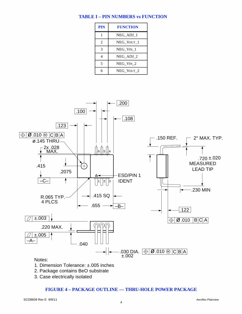
FIGURE 4 – PACKAGE OUTLINE — THRU-HOLE POWER PACKAGE
3
456
21
PIN NUMBERS vs FUNCTION
PIN FUNCTION
1 POS_ADJ_1
2 POS_VOUT_1
3 POS_VIN_1
4 NEG_ADJ_2
5 NEG_VIN_2
6 NEG_VOUT_2
2x .028
Mø.010 C B A
.230 MIN
Notes: 1. Dimension Tolerance: ±.005 inches2. Package contains BeO substrate3. Case electrically isolated
.122
MAX.

6SCD8601 Rev T 9/9/11 Aeroflex Plainview
.108
.200
.100
.123
ø.145 THRU
.415.2075
R.065 TYP.4 PLCS
.655
.415 SQ
±.003
.220 MAX.
±.005
.040 ±.002.030 DIA.
.122
.150 REF.
±.020.886
IDENTESD/PIN 1
–B–
–A–
–C–
ø.010 B C A
Mø.010 C B A
Notes:
FIGURE 5 – PACKAGE OUTLINE — SURFACE MOUNT POWER PACKAGE
1. Dimension Tolerance: ±.005 inches2. Package contains BeO substrate
3
456
21
PIN NUMBERS vs FUNCTION
PIN FUNCTION
1 POS_ADJ_1
2 POS_VOUT_1
3 POS_VIN_1
4 NEG_ADJ_2
5 NEG_VIN_2
6 NEG_VOUT_2
2x .028
Mø.010 C B A.020
.060
3. Case electrically isolated
MAX.

77SCD8601 Rev T 9/9/11
PLAINVIEW, NEW YORKToll Free: 800-THE-1553 Fax: 516-694-6715
SE AND MID-ATLANTIC Tel: 321-951-4164 Fax: 321-951-4254
INTERNATIONALTel: 805-778-9229Fax: 805-778-1980
WEST COAST Tel: 949-362-2260Fax: 949-362-2266
NORTHEASTTel: 603-888-3975Fax: 603-888-4585
CENTRALTel: 719-594-8017Fax: 719-594-8468
w w w . a e r o f l e x . c o m i n f o - a m s @ a e r o f l e x . c o m
Aeroflex Microelectronic Solutions reserves the right to change at any time without notice the specifications, design, function, or form of its products described herein. All parameters must be validated for each customer's application by engineering. No liability is assumed as a result of use of this product. No patent licenses are implied.
EXPORT CONTROL: EXPORT WARNING:This product is controlled for export under the International Traffic inArms Regulations (ITAR). A license from the U.S. Department ofState is required prior to the export of this product from the UnitedStates.
Aeroflex’s military and space products are controlled for export underthe International Traffic in Arms Regulations (ITAR) and may not besold or proposed or offered for sale to certain countries. (See ITAR126.1 for complete information.)
Our passion for performance is defined by threeattributes represented by these three icons:solution-minded, performance-driven and customer-focused
and the Linear Technology logo are registered trademarks and RH117 & RH137 are a copyright of Linear Technology Corporation.
ORDERING INFORMATION
MODEL DLA SMD # SCREENING PACKAGE
VRG8601-7 - Commercial Flow, +25°C testing only
6 Lead Thru-Hole
Power Pkg
VRG8601-S -Military Temperature, -55°C to +125°C
Screened in accordance with the individual Test Methodsof MIL-STD-883 for Space Applications
VRG8601-201-1S 5962-0521901KXCIn accordance with DLA SMD
VRG8601-201-2S 5962-0521901KXA
VRG8601-901-1S 5962R0521901KXC In accordance with DLA Certified RHA Program Planto RHA level "R", 100 krads(Si) VRG8601-901-2S 5962R0521901KXA
VRG8602-7 - Commercial Flow, +25°C testing only
6 Lead Surface Mount
Power Pkg
VRG8602-S -Military Temperature, -55°C to +125°C
Screened in accordance with the individual Test Methodsof MIL-STD-883 for Space Applications
VRG8602-201-1S 5962-0521901KYCIn accordance with DLA SMD
VRG8602-201-2S 5962-0521901KYA
VRG8602-901-1S 5962R0521901KYC In accordance with DLA Certified RHA Program Planto RHA level "R", 100 krads(Si) VRG8602-901-2S 5962R0521901KYA

SCD8607 Rev E
Manufactured using Linear Technology Corporation ® Space Qualified RH117 die Radiation performance
- Total dose: 100 krads(Si), Dose rate = 50 - 300 rads(Si)/s
- ELDRS: 50 krads(Si), Dose rate < 10 mrads(Si)/s
Thermal shutdown Output voltage adjustable: 1.25V to 37V 3-Terminal Output current: 1.5A Voltage reference: 1.25V
Load regulation: 1.9% max Line regulation: 0.06%/V max Ripple rejection: >66dB Packaging – Hermetic metal
- Thru-hole or Surface mount- 6 Leads, .655"L x .415"W x .200"Ht- Power package- Weight - 5 gm max
Designed for aerospace and high reliability space applications
DESCRIPTIONThe Aeroflex Plainview VRG8607/08 consists of two positive (RH117) voltage regulators each capable of supplyingin excess of 1.5Amps over the output voltage range as defined under recommended operating conditions. Eachregulator is exceptionally easy to set-up, requiring only 2 external resistors to set the output voltage. The moduledesign has been optimized for excellent regulation and low thermal transients. There is full electrical isolationbetween the regulators and each regulator to the package.
Further, the VRG8607/08 features internal current limiting, thermal shutdown and safe-area compensation, makingthem virtually blowout-proof against overloads. The VRG8607/08 serves a wide variety of applications includinglocal on-card regulation, programmable output voltage regulation or precision current regulation.
The VRG8607/08 has been specifically designed to meet exposure to radiation environments. The VRG8607 isconfigured for a Thru-Hole 6 lead metal power package and the VRG8608 is configured for a Surface Mount 6 leadmetal power package. It is guaranteed operational from -55°C to +125°C. Available screened to MIL-STD-883, theVRG8607/08 is ideal for demanding military and space applications.
For detailed performance characteristic curves, applications information and typical applications see the
latest Linear Technology Corporation ® data sheets for their RH/LT117, which is available on-line atwww.linear.com.
VRG8607/08
Radiation Tolerant
5
VIN
ADJ
VOUT
4
3
VIN
ADJ
VOUT
1
FIGURE 1 – BLOCK DIAGRAM / SCHEMATIC
September 9, 2011
www.aeroflex.com/voltreg
Standard Products
2 6
Dual Adjustable Positive Voltage Regulators
RH117Positive
Regulator
RH117Positive
Regulator
FEATURES
Aeroflex Plainview’s Radiation Hardness Assurance Plan is DLA Certified to MIL-PRF-38534, Appendix G.

2SCD8607 Rev E 9/9/11 Aeroflex Plainview
ABSOLUTE MAXIMUM RATINGS
PARAMETER RANGE UNITS
Operating (Junction) Temperature Range -55 to +150 C
Lead Temperature (soldering, 10 sec) 300 °C
Storage Temperature Range -65 to +150 C
Input-Output Voltage Differential 40 (Pos) V
Thermal Resistance (Junction to case JC) each Regulator 5 °C/W
ESD Rating 1.999 1/ KV
1/ Meets ESD testing per MIL-STD-883, method 3015, Class 1C.
NOTICE: Stresses above those listed under "Absolute Maximums Rating" may cause permanent damage to the device. These are stress rating only; functional operation beyond the "Operation Conditions" is not recommended and extended exposure beyond the "Operation Conditions" may effect device reliability.
RECOMMENDED OPERATING CONDITIONS
PARAMETER RANGE UNITS
Output Voltage Range 1.3 to 37 VDC
Case Operating Temperature Range -55 to +125 °C
ELECTRICAL PERFORMANCE CHARACTERISTICS 1/
PARAMETER SYM CONDITIONS (P PMAX MIN MAX UNITS
Reference Voltage 4/ VREF 3V < (VIN - VOUT) < VDIFF MAX, 10mA < IOUT < IMAX 1.200 1.300 V
Line Regulation 2/ 4/ 3V < (VIN - VOUT) < VDIFF MAX, IOUT = 10mA - 0.03 %/V
Load Regulation 2/ 4/ 10mA < IOUT < IMAX, VOUT < 5V10mA < IOUT < IMAX, VOUT > 5V
--
601.2
mV%
Thermal Regulation IOUT = 1.5A, (VIN - VOUT) = 13.3V, 20ms Pulse, 20W,TC = +25°C
- 0.07 %/W
Ripple Rejection Ratio VOUT = 10V, f = 120Hz, CADJ = 10µF 66 - dB
Adjustment Pin Current 4/ IADJ IOUT = 10mA, 3V < (VIN - VOUT) < 40V - 100 µA
Adjustment Pin Current Change 4/ IADJ
10mA < IOUT < IMAX3.0V < (VIN - VOUT) < 40V - 5 µA
Minimum Load Current 3/ 4/ IMIN (VIN - VOUT) = 40V - 5 mA
Current Limit 4/ 5/ IMAX(VIN - VOUT) < 15V 1.5 -
A(VIN - VOUT) = 40V, TC = +25°C 0.30 -
Long Term Stability 3/ TC = +125°C - 1 %
Thermal Resistance, each Regulator(Junction to Case) 3/
JC - 5 °C/W
Notes:1/ Unless otherwise specified, these specifications apply for (Vin - Vout) = 5V, Iout = 0.5A and -55°C < Tc < +125°C.2/ Regulation is measured at a constant junction temperature, using pulse testing with a low duty cycle. Changes in output voltage due to
heating effects are covered under the specification for thermal regulation. Measurements taken at the output lead must be adjusted for lead resistance.
3/ Not tested. Shall be guaranteed to the specified limits. 4/ Specification derated to reflect High Dose Rate (1019 condition A) to 100 krad(Si) and Low Dose Rate (1019 condition D) to 50 krad(Si),
@ +25°C.5/ Pulsed @ < 10% duty cycle @ +25°C.
VOUTVIN
VOUTIOUT
VOUTTIME

3SCD8607 Rev E 9/9/11 Aeroflex Plainview
The maximum Power dissipation is limited by the thermal shutdown function of each regulator chip in the VRG8607/08. Thegraph above represents the achievable power before the chip shuts down. The first line in the graph represents the maximumpower dissipation of the VRG8607/08 with one regulator on (the other off) and the other line represents both regulators ondissipating equal power. If both regulators are on and one regulator is dissipating more power that the other, the maximum powerdissipation of the VRG8607/08 will fall between the two lines. This graph is based on the maximum junction temperature of150°C and a thermal resistance (JC) of 5°C/W.
60
50
40
30
20
10
0 20 40 60 80 100 120 140
Case Temperature (°C)
1 Regulator
0
Both RegulatorsMaximum Power
Dissipation(Watts)
IADJ = 50µAVREF = 1.25V,
+Reg = VOUT = VREF (1+R2/R1) + (IADJ x R2)
VRG8607/08VIN VOUT
ADJ
R1
R2
VREF
Adjustable Regulator
FIGURE 3 – TYPICAL APPLICATIONS
FIGURE 2 – MAXIMUM POWER vs CASE TEMPERATURE

4SCD8607 Rev E 9/9/11 Aeroflex Plainview
.108
.200
.100
.123
ø.145 THRU
.415.2075
R.065 TYP.4 PLCS
.655
.415 SQ
±.003
.220 MAX.
±.005
.040
±.002.030 DIA.
.150 REF. 2° MAX. TYP.
±.020.720MEASURED
LEAD TIP
IDENTESD/PIN 1
–B–
–A–
–C–
ø.010 B C A
Mø.010 C B A
FIGURE 4 – PACKAGE OUTLINE — THRU-HOLE POWER PACKAGE
3
456
21
TABLE I – PIN NUMBERS vs FUNCTION
PIN FUNCTION
1 POS_ADJ_1
2 POS_VOUT_1
3 POS_VIN_1
4 POS_ADJ_2
5 POS_VIN_2
6 POS_VOUT_2
2x .028
Mø.010 C B A
.230 MIN
Notes: 1. Dimension Tolerance: ±.005 inches2. Package contains BeO substrate3. Case electrically isolated
.122
MAX.

5SCD8607 Rev E 9/9/11 Aeroflex Plainview
.108
.200
.100
.123
ø.145 THRU
.415.2075
R.065 TYP.4 PLCS
.655
.415 SQ
±.003
.220 MAX.
±.005
.040 ±.002.030 DIA.
.122
.150 REF.
±.020.886
IDENTESD/PIN 1
–B–
–A–
–C–
ø.010 B C A
Mø.010 C B A
Notes:
FIGURE 5 – PACKAGE OUTLINE — SURFACE MOUNT POWER PACKAGE
1. Dimension Tolerance: ±.005 inches2. Package contains BeO substrate
3
456
21
TABLE II – PIN NUMBERS vs FUNCTION
PIN FUNCTION
1 POS_ADJ_1
2 POS_VOUT_1
3 POS_VIN_1
4 POS_ADJ_2
5 POS_VIN_2
6 POS_VOUT_2
2x .028
Mø.010 C B A.020
.060
3. Case electrically isolated
MAX.

6SCD8607 Rev E 9/9/11
PLAINVIEW, NEW YORKToll Free: 800-THE-1553 Fax: 516-694-6715
SE AND MID-ATLANTIC Tel: 321-951-4164 Fax: 321-951-4254
INTERNATIONALTel: 805-778-9229Fax: 805-778-1980
WEST COAST Tel: 949-362-2260Fax: 949-362-2266
NORTHEASTTel: 603-888-3975Fax: 603-888-4585
CENTRALTel: 719-594-8017Fax: 719-594-8468
w w w . a e r o f l e x . c o m i n f o - a m s @ a e r o f l e x . c o m
Aeroflex Microelectronic Solutions reserves the right to change at any time without notice the specifications, design, function, or form of its products described herein. All parameters must be validated for each customer's application by engineering. No liability is assumed as a result of use of this product. No patent licenses are implied.
EXPORT CONTROL: EXPORT WARNING:This product is controlled for export under the International Traffic inArms Regulations (ITAR). A license from the U.S. Department ofState is required prior to the export of this product from the UnitedStates.
Aeroflex’s military and space products are controlled for export underthe International Traffic in Arms Regulations (ITAR) and may not besold or proposed or offered for sale to certain countries. (See ITAR126.1 for complete information.)
Our passion for performance is defined by threeattributes represented by these three icons:solution-minded, performance-driven and customer-focused
and the Linear Technology logo are registered trademarks and RH117 are a copyright of Linear Technology Corporation.
ORDERING INFORMATION
MODEL DLA SMD # SCREENING PACKAGE
VRG8607-7 - Commercial Flow, +25°C testing only
6 Lead Thru-Hole
Power Pkg
VRG8607-S -Military Temperature, -55°C to +125°C
Screened in accordance with the individual Test Methodsof MIL-STD-883 for Space Applications
VRG8607-201-1S 5962-0521903KXCIn accordance with DLA SMD
VRG8607-201-2S 5962-0521903KXA
VRG8607-901-1S 5962R0521903KXC In accordance with DLA Certified RHA Program Planto RHA level "R", 100 krads(Si)VRG8607-901-2S 5962R0521903KXA
VRG8608-7 - Commercial Flow, +25°C testing only
6 Lead Surface Mount
Power Pkg
VRG8608-S -Military Temperature, -55°C to +125°C
Screened in accordance with the individual Test Methodsof MIL-STD-883 for Space Applications
VRG8608-201-1S 5962-0521903KYCIn accordance with DLA SMD
VRG8608-201-2S 5962-0521903KYA
VRG8608-901-1S 5962R0521903KYC In accordance with DLA Certified RHA Program Planto RHA level "R", 100 krads(Si)VRG8608-901-2S 5962R0521903KYA
SCD8609 Rev E
DESCRIPTIONThe Aeroflex Plainview VRG8609/10 consists of two negative (RH137) voltage regulators each capable of supplyingin excess of 1.5Amps over the output voltage range as defined under recommended operating conditions. Eachregulator is exceptionally easy to set-up, requiring only 2 external resistors to set the output voltage. The moduledesign has been optimized for excellent regulation and low thermal transients. There is full electrical isolationbetween the regulators and each regulator to the package.
Further, the VRG8609/10 features internal current limiting, thermal shutdown and safe-area compensation, makingthem virtually blowout-proof against overloads. The VRG8609/10 serves a wide variety of applications includinglocal on-card regulation, programmable output voltage regulation or precision current regulation.
The VRG8609/10 has been specifically designed to meet exposure to radiation environments. The VRG8609 isconfigured for a Thru-Hole 6 lead metal power package and the VRG8610 is configured for a Surface Mount 6 leadmetal power package. It is guaranteed operational from -55°C to +125°C. Available screened to MIL-STD-883, theVRG8609/10 is ideal for demanding military and space applications.
For detailed performance characteristic curves, applications information and typical applications see thelatest Linear Technology Corporation ® data sheets for their RH/LT137, which is available on-line atwww.linear.com.
VRG8609/10
Radiation Tolerant
5
VIN
ADJ
VOUT
4
3
VIN
ADJ
VOUT
1
FIGURE 1 – BLOCK DIAGRAM / SCHEMATIC
September 9, 2011
www.aeroflex.com/voltreg
Standard Products
2 6
Dual Adjustable Negative Voltage Regulators
RH137NegativeRegulator
RH137NegativeRegulator
FEATURES
Manufactured using Linear Technology Corporation ® Space Qualified RH137 die Radiation performance
- Total dose: 100 krads(Si), Dose rate = 50 - 300 rads(Si)/s
- ELDRS: 50 kreds(Si),Dose rate < 10 mrads(Si)/S
Thermal shutdown Output voltage adjustable: -1.25V to -27V 3-Terminal Output current: 1.5A Voltage reference: -1.25V
Load regulation: 1.0% max Line regulation: 0.05% max Ripple rejection: >66dB Packaging – Hermetic metal
- Thru-hole or Surface mount- 6 Leads, .655"L x .415"W x .200"Ht- Power package- Weight - 5 gm max
Designed for aerospace and high reliability space applications
Aeroflex Plainview’s Radiation Hardness Assurance Plan is DLA Certified to MIL-PRF-38534, Appendix G.

2SCD8609 Rev E 9/9/11 Aeroflex Plainview
ABSOLUTE MAXIMUM RATINGS
PARAMETER RANGE UNITS
Operating (Junction) Temperature Range -55 to +150 C
Lead Temperature (soldering, 10 sec) 300 °C
Storage Temperature Range -65 to +150 C
Input-Output Voltage Differential 30 (Neg) V
Thermal Resistance (junction to case JC) each, Pos. & Neg. 5 °C/W
ESD Rating 1.999 1/ KV
1/ Meets ESD testing per MIL-STD-883, method 3015, Class 1C.
NOTICE: Stresses above those listed under "Absolute Maximums Rating" may cause permanent damage to the device. These are stress rating only; functional operation beyond the "Operation Conditions" is not recommended and extended exposure beyond the "Operation Conditions" may effect device reliability.
RECOMMENDED OPERATING CONDITIONS
PARAMETER RANGE UNITS
Output Voltage Range -1.3 to -27 VDC
Case Operating Temperature Range -55 to +125 °C
ELECTRICAL PERFORMANCE CHARACTERISTICS 1/
PARAMETER SYM CONDITIONS (P PMAX MIN MAX UNITS
Reference Voltage 4/ VREF 3V < (VIN - VOUT) < VDIFF MAX, 10mA < IOUT < IMAX -1.200 -1.300 V
Line Regulation 2/, 4/ 3V < (VIN - VOUT) < 30V, - 0.05 %/V
Load Regulation 2/, 4/ 10mA < IOUT < IMAX, VOUT < 5V10mA < IOUT < IMAX, VOUT > 5V
--
501.0
mV%
Thermal Regulation IOUT = 1.5A, (VIN - VOUT) = 13.3V, 20ms Pulse, 20W, TC = +25°C - 0.02 %/W
Ripple Rejection VOUT = -10V, f = 120Hz, CADJ = 10µF 66 - dB
Adjustment Pin Current 4/ IADJ IOUT = 10mA, 3V < (VIN - VOUT) < 30V - 100 µA
Adjustment Pin Current Change 4/ IADJ 3V < (VIN - VOUT) < 30V, 10mA < IOUT < IMAX - 5 µA
Minimum Load Current 3/ 4/ IMIN(VIN - VOUT) = 30V - 5
mA(VIN - VOUT) < 10V - 3
Current Limit 4/, 5/ IMAX(VIN - VOUT) < 15V 1.5 -
A(VIN - VOUT) = 30V, TC = +25°C 0.24 -
Long Term Stability 3/ TC = +125°C - 1 %
Thermal Resistance, each Regulator (Junction to Case) 3/
JC - 5 °C/W
Notes:1/ Unless otherwise specified, these specifications apply for, (Vin - Vout) = 5V, Iout = 0.5A and -55°C < Tc < +125°C.2/ Regulation is measured at a constant junction temperature, using pulse testing with a low duty cycle. Changes in output voltage due to
heating effects are covered under the specification for thermal regulation. Measurements taken at the output lead must be adjusted for lead resistance.
3/ Not tested. Shall be guaranteed to the specified limits. 4/ Specification derated to reflect High Dose Rate (1019 condition A) to 100krads(Si) and Low Dose Rate (1019 condition D) to
50krads(Si), @ +25°C.5/ Pulsed @ < 10% duty cycle @ +25°C.
VOUTVIN
VOUTIOUT
VOUTTIME

3SCD8609 Rev E 9/9/11 Aeroflex Plainview
The maximum Power dissipation is limited by the thermal shutdown function of each regulator chip in the VRG8609/10. Thegraph above represents the achievable power before the chip shuts down. The first line in the graph represents the maximumpower dissipation of the VRG8609/10 with one regulator on (the other off) and the other line represents both regulators ondissipating equal power. If both regulators are on and one regulator is dissipating more power that the other, the maximum powerdissipation of the VRG8609/10 will fall between the two lines. This graph is based on the maximum junction temperature of150°C and a thermal resistance (JC) of 5°C/W.
60
50
40
30
20
10
0 20 40 60 80 100 120 140
Case Temperature (°C)
1 Regulator
0
Both RegulatorsMaximum Power
Dissipation(Watts)
IADJ = 50µAVREF = 1.25V,
-Reg = VOUT = -VREF (1+R2/R1) + (-IADJ x R2)
Adjustable Regulator
VRG8609/10VIN VOUT
ADJ
R1
R2
VREF
FIGURE 2 – MAXIMUM POWER vs CASE TEMPERATURE
FIGURE 3 – TYPICAL APPLICATIONS
4SCD8609 Rev E 9/9/11 Aeroflex Plainview
TABLE I – PIN NUMBERS vs FUNCTION
PIN FUNCTION
1 NEG_ADJ_1
2 NEG_VOUT_1
3 NEG_VIN_1
4 NEG_ADJ_2
5 NEG_VIN_2
6 NEG_VOUT_2
.108
.200
.100
.123
ø.145 THRU
.415.2075
R.065 TYP.4 PLCS
.655
.415 SQ
±.003
.220 MAX.
±.005
.040
±.002.030 DIA.
.150 REF. 2° MAX. TYP.
±.020.720MEASURED
LEAD TIP
IDENTESD/PIN 1
–B–
–A–
–C–
ø.010 B C A
Mø.010 C B A
FIGURE 4 – PACKAGE OUTLINE — THRU-HOLE POWER PACKAGE
3
456
21
2x .028
Mø.010 C B A
.230 MIN
Notes: 1. Dimension Tolerance: ±.005 inches2. Package contains BeO substrate3. Case electrically isolated
.122
MAX.

5SCD8609 Rev E 9/9/11 Aeroflex Plainview
TABLE II – PIN NUMBERS vs FUNCTION
PIN FUNCTION
1 NEG_ADJ_1
2 NEG_VOUT_1
3 NEG_VIN_1
4 NEG_ADJ_2
5 NEG_VIN_2
6 NEG_VOUT_2
.108
.200
.100
.123
ø.145 THRU
.415.2075
R.065 TYP.4 PLCS
.655
.415 SQ
±.003
.220 MAX.
±.005
.040 ±.002.030 DIA.
.122
.150 REF.
±.020.886
IDENTESD/PIN 1
–B–
–A–
–C–
ø.010 B C A
Mø.010 C B A
Notes:
FIGURE 5 – PACKAGE OUTLINE — SURFACE MOUNT POWER PACKAGE
1. Dimension Tolerance: ±.005 inches2. Package contains BeO substrate
3
456
21
2x .028
Mø.010 C B A.020
.060
3. Case electrically isolated
MAX.

6SCD8609 Rev E 9/9/11
PLAINVIEW, NEW YORKToll Free: 800-THE-1553 Fax: 516-694-6715
SE AND MID-ATLANTIC Tel: 321-951-4164 Fax: 321-951-4254
INTERNATIONALTel: 805-778-9229Fax: 805-778-1980
WEST COAST Tel: 949-362-2260Fax: 949-362-2266
NORTHEASTTel: 603-888-3975Fax: 603-888-4585
CENTRALTel: 719-594-8017Fax: 719-594-8468
w w w . a e r o f l e x . c o m i n f o - a m s @ a e r o f l e x . c o m
Aeroflex Microelectronic Solutions reserves the right to change at any time without notice the specifications, design, function, or form of its products described herein. All parameters must be validated for each customer's application by engineering. No liability is assumed as a result of use of this product. No patent licenses are implied.
EXPORT CONTROL: EXPORT WARNING:This product is controlled for export under the International Traffic inArms Regulations (ITAR). A license from the U.S. Department ofState is required prior to the export of this product from the UnitedStates.
Aeroflex’s military and space products are controlled for export underthe International Traffic in Arms Regulations (ITAR) and may not besold or proposed or offered for sale to certain countries. (See ITAR126.1 for complete information.)
Our passion for performance is defined by threeattributes represented by these three icons:solution-minded, performance-driven and customer-focused
and the Linear Technology logo are registered trademarks and RH137 are a copyright of Linear Technology Corporation.
ORDERING INFORMATION
MODEL DLA SMD # SCREENING PACKAGE
VRG8609-7 - Commercial Flow, +25°C testing only
6 LeadThru-HolePower Pkg
VRG8609-S -Military Temperature, -55°C to +125°C
Screened in accordance with the individual Test Methodsof MIL-STD-883 for Space Applications
VRG8609-201-1S 5962-0521904KXCIn accordance with DLA SMD
VRG8609-201-2S 5962-0521904KXA
VRG8609-901-1S 5962R0521904KXC In accordance with DLA Certified RHA Program Planto RHA level "R", 100 krads(Si)VRG8609-901-2S 5962R0521904KXA
VRG8610-7 - Commercial Flow, +25°C testing only
6 LeadSurface Mount
Power Pkg
VRG8610-S -Military Temperature, -55°C to +125°C
Screened in accordance with the individual Test Methodsof MIL-STD-883 for Space Applications
VRG8610-201-1S 5962-0521904KYCIn accordance with DLA SMD
VRG8610-201-2S 5962-0521904KYA
VRG8610-901-1S 5962R0521904KYC In accordance with DLA Certified RHA Program Planto RHA level "R", 100 krads(Si)VRG8610-901-2S 5962R0521904KYA

SCD8651 Rev H
Manufactured using Space Qualified RH1086 and RH1185 die Radiation performance
- Total dose > 100 krad (Si), Dose rate = 50 - 300 rads(Si)/s
Two-Independent voltage regulators Thermal shutdown Adjustable Output Voltages
Positive regulator features (RH1086)– Output voltage adjustable: 1.25V to 23V– Dropout voltage: 1.3V at 1.0 Amps– 3-Terminal – Output current: 1.0A, See note 13 – Voltage reference: 1.25V +2%, -3.2%– Load regulation: 0.3% max– Line regulation: 0.25% max– Ripple rejection: >60dB
Packaging – Hermetic metal– Thru-hole or Surface mount– 8 Leads, .755"L x .415"W x .200"Ht– Power package– Weight - 6 gm max
Designed for aerospace and high reliability space applications
Negative regulator features (RH1185)– Output voltage adjustable: -2.37 to -25V– Dropout voltage: 1.05V at 3Amps– 5-Terminal – Output current: 3A – Voltage reference: -2.370V ±3%– Load regulation: 0.8% max– Line regulation: 0.02% max– Ripple rejection: >60dB
DESCRIPTIONThe Aeroflex Plainview VRG8651/8652 consists of one Positive Adjustable (RH1086) and one Negative Adjustable(RH1185) LDO voltage regulator capable of supplying 1.0Amps (RH1086) /3Amps(RH1185) respectively over theoutput voltage range as defined under recommended operating conditions. The VRG8651/8652 offers excellent lineand load regulation specifications and ripple rejection. There is full electrical isolation between the regulators andeach regulator to the package.
The VRG8651/8652 serves a wide variety of applications including SCSI-2 Active Terminator, High EfficiencyLinear Regulators, Post Regulators for Switching Supplies, Constant Current Regulators, Battery Chargers andMicroprocessor Supply.
The VRG8651/8652 has been specifically designed to meet exposure to radiation environments. The VRG8651 isconfigured for a Thru-Hole 8 lead metal power package and the VRG8652 is configured for a Surface Mount 8 leadmetal power package. It is guaranteed operational from -55°C to +125°C. Available screened to MIL-STD-883, theVRG8651/8652 is ideal for demanding military and space applications.
Dropout (VIN - VOUT) decreases at lower load currents for both regulators.
VIN
ADJ
VOUT
FIGURE 1 – BLOCK DIAGRAM / SCHEMATIC
January 10, 2012
Standard Products
7
PositiveRegulator
FEATURES
6GND
VOUT
RH1185
Feedback
VIN
2
3
5
RH1086
PositiveRegulator
NegativeRegulator
4
Reference
8
1
Radiation Tolerant
VRG8651/VRG8652 Dual Voltage Regulator, 1.0 Amp Pos and 3.0 Amp Neg Low Dropout (LDO), Adjustable
www.aeroflex.com/voltreg
Aeroflex Plainview’s Radiation Hardness Assurance Plan is DLA Certified to MIL-PRF-38534, Appendix G.
2SCD8651 Rev H 1/10/12 Aeroflex Plainview
ABSOLUTE MAXIMUM RATINGS
PARAMETERRANGE
UNITSRH1086 RH1185
Input Voltage 25+VREF -35 VDC
Lead temperature (soldering 10 Sec) 300 °CInput Output Differential 25 30 VDC
Feedback & Reference Voltage - -7 VDC
Output Voltage +25 -30 VDC
DC Output Current 1.5 - AESD 2000 1/ VOperating Junction Temperature Range -55 to +150 °CStorage Temperature Range -65 to +150 °C
1/ Meets ESD testing per MIL-STD-883, method 3015, Class 1C.NOTICE: Stresses above those listed under "Absolute Maximums Rating" may cause permanent damage to the device. These are
stress rating only; functional operation beyond the "Operation Conditions" is not recommended and extended exposure beyond the "Operation Conditions" may effect device reliability.
RECOMMENDED OPERATING CONDITIONS
PARAMETERRANGE
UNITSRH1086 RH1185
Output Voltage Range 1.275 to 23 -2.45 to -25 VDC
Input Output Differential 1.5 to 25 1 to 28 VDC
Case Operating Temperature Range -55 to +125 °C
Thermal Resistance, Junction to case jc 5 °C/W
ELECTRICAL PERFORMANCE CHARACTERISTICSUnless otherwise specified, these specifications apply for post radiation and -55°C < Tc < +125°C.
PARAMETER SYM CONDITIONS (PPMAX) MIN MAX UNITS
RH1086 Positive LDO section only
Reference Voltage 2/ 3/ VREF 1.5V < VIN - VOUT < 15V, ILOAD = 10mA 1.210 1.275 V
Line Regulation 2/ 3/ ILOAD = 10mA, 1.5V < VIN - VOUT < 15V - 0.25 %
Load Regulation 2/ 3/ 10mA < IOUT < 1.0A, VIN - VOUT = 3V - 0.3 %
Dropout Voltage 2/ 4/ VDROP VREF = 1%, IOUT = 1.0A - 1.30 V
Adjust Pin Current 2/ - - 120 µA
Adjust Pin Current Change 2/ - 10 mA < IOUT < 1.0A, 1.5V < VIN - VOUT < 15V - 5 µA
Current Limit 2/ 14/ IMAXVIN - VOUT = 5V VIN - VOUT < 25V
1.50.047
--
AA
Minimum Load Current 5/ IMIN VIN - VOUT = 25V - 10 mA
Ripple Rejection 3/ - IOUT = 1.0A, VIN - VOUT = 3V, f = 120Hz, CADJ = COUT = 25µF 60 - dB
Thermal Regulation 30ms pulse, TC = +25°C - 0.04 %/W
VREF Long-Term Stability 5/ Burn In: TC = +125°C @ 1000hrs min, tested @ 25°C - 0.3 %
VOUTVIN
VOUTIOUT

3SCD8651 Rev H 1/10/12 Aeroflex Plainview
RH1185 Negative LDO section only 1/, 9/
Reference Voltage (At pin 6) 2/ 9/ VREF 1mA < IOUT < 3A, VIN - VOUT = 1.2V to 28V, VOUT = -5V -2.29 -2.45 V
Dropout Voltage 2/ 6/ VDROPIOUT = 0.5A, VOUT = -5V - 0.425 V
IOUT = 3A, VOUT = -5V - 1.05 V
Line Regulation 2/ 10/ 1.0V < VIN - VOUT < 20V, VOUT = -5V - 0.02 %/V
Load Regulation 2/ 10/ 5mA < IOUT < 3A, VIN - VOUT = 1.5V to 10V, VOUT = -5V - 0.8 %
Minimum Input Voltage 2/ 7/ VIN MIN IOUT = 3A , VOUT = VREF - -4.50 V
Internal Current Limit (See Graph for Guaranteed Curve - See Figure 6) 2/ 14/
ICL
1.5V < VIN - VOUT < 10V 3.3 4.55 A
VIN - VOUT = 15V 2.0 4.5 A
VIN - VOUT = 20V 1.0 3.1 A
VIN - VOUT = 30V 5/ 0.2 1.6 A
External Current Limit 2/ ILIMRLIM = 5K 12/ 2.7 3.7 A
RLIM = 15K 12/ 0.9 1.6 A
Quiescent Supply Current 2/ 8/ IQ IOUT = 5mA, VOUT = VREF, -4V < VIN < -25V - 3.5 mA
Supply Current Change with Load 2/ IQ
VIN – VOUT = VSAT 11/ - 35 mA/A
VIN – VOUT 2V - 21 mA/A
Ripple Rejection - IOUT = 1.0A, VIN - VOUT = 3V, f = 120Hz, 60 - dB
Thermal Regulation (See application information LT1185) 5/
- VIN –VOUT = 10V, IOUT = 5mA to 2A, TC = +25°C - 0.014 %/W
Notes1. Meets ESD testing per MIL-STD-883, method 3015, Class 2.2. Specification derated to reflect High Dose Rate (1019 condition A) to 100Krad (Si) @ +25°C.3. Line and load regulation are guaranteed up to the maximum power dissipation of 15W. Power dissipation is determined by the
input/output differential voltage and the output current. Guaranteed maximum power dissipation will not be available over thefull input/output voltage range.
4. Dropout voltage is specified over the full output current range of the device. 5. Not tested. Shall be guaranteed by design, characterization, or correlation to other tested parameters. 6. Dropout voltage is tested by reducing input voltage until the output drops 1% below its nominal value. Tests are done at 0.5A
and 3A. The power transistor looks basically like a pure resistance in this range so that minimum differential at anyintermediate current can be calculated by interpolation; VDROPOUT = 0.25V + (0.25 x IOUT). For load current less than 0.5A,see Figure 4.
7. “Minimum input voltage” is limited by base emitter voltage drive of the power transistor section, not saturation as measured inNote 6. For output voltages below 4V, “minimum input voltage” specification may limit dropout voltage before transistorsaturation limitation.
8. Supply current is measured on the ground pin, and does not include load current, RLIM, or output divider current.9. The 25W power level is guaranteed for an input-output voltage of 8.3V to 17V. At lower voltages the 3A limit applies, and at
higher voltages the internal power limiting may restrict regulator power below 25W.10. Line and load regulation are measured on a pulse basis with a pulse width of 2ms, to minimize heating. DC regulation will be
affected by thermal regulation and temperature coefficient of the reference.11. VSAT is the maximum specified dropout voltage; 0.25V +(0.25 x IOUT).12. Current limit is programmed with a resistor from REF pin to GND pin. RLIM = 15K/ILIM.13. For compliance with MIL-STD- 883 revision C current density specification, the RH1086MK is derated to 1 Amp but is capable
of 1.5 Amps.14. Pulsed @ <10% duty cycle @ +25°C.
ELECTRICAL PERFORMANCE CHARACTERISTICSUnless otherwise specified, these specifications apply for post radiation and -55°C < Tc < +125°C.
PARAMETER SYM CONDITIONS (PPMAX) MIN MAX UNITS
VOUTVIN
VOUTIOUT
4SCD8651 Rev H 1/10/12 Aeroflex Plainview
FIGURE 2 – MAXIMUM POWER vs CASE TEMPERATURE
60
50
40
30
20
10
0 20 40 60 80 100 120 140
Case Temperature (°C)
1 Regulator
0
Both RegulatorsMaximum Power
Dissipation(Watts)
The maximum Power dissipation is limited by the thermal shutdown function of each regulator chip in theVRG8651/8652. The graph above represents the achievable power before the chip shuts down. The first line in thegraph represents the maximum power dissipation of the VRG8651/8652 with one regulator on (the other off) and theother line represents both regulators on dissipating equal power. If both regulators are on and one regulator isdissipating more power that the other, the maximum power dissipation of the VRG8651/8652 will fall between the twolines. This graph is based on the maximum junction temperature of 150°C and a thermal resistance (JC) of 5°C/W.

5SCD8651 Rev H 1/10/12 Aeroflex Plainview
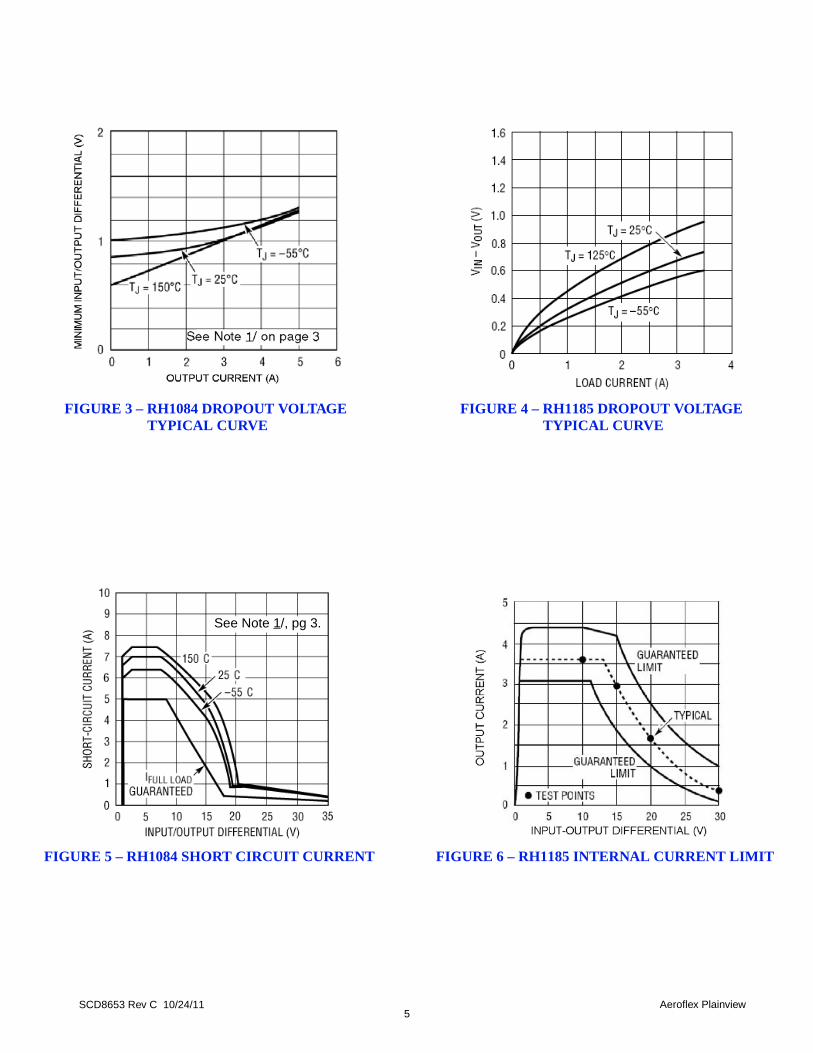
FIGURE 4 – RH1185 DROPOUT VOLTAGE FIGURE 3 – RH1086 DROPOUT VOLTAGE
FIGURE 5 – RH1086 SHORT CIRCUIT CURRENT FIGURE 6 – RH1185 INTERNAL CURRENT LIMIT
See Note 13, pg 3.
TYPICAL CURVETYPICAL CURVE
See Note 13, pg 3.

6SCD8651 Rev H 1/10/12 Aeroflex Plainview
FIGURE 8 – BASIC RH1185 ADJUSTABLE REGULATOR APPLICATION
R1 & R2 LOCATION & PROPER CONNECTION OF POSITIVE SENSE LEAD
FIGURE 7 – BASIC RH1086 ADJUSTABLE REGULATOR APPLICATION
VRG8651/52VIN Vout
ADJ
R1
R2
VREF10µFTant.
IADJ = 50µAVREF = 1.25V,+Reg = VOUT = VREF (1+R2/R1) + (IADJ x R2)
8 7
1
10µFTant.
SETTING OUTPUT VOLTAGE
(RH1086)
The RH1185 output voltage is set by two external resistors. The internal reference voltage is trimmed to 2.37V so that a standard 1% 2.37k resistor (R1) can be used to set divider current at 1mA. R2 is then selected from:
for R1 = 2.37k and VREF = 2.37V, this reduces to:
suggested values of 1% resistors are shown below:
R2 =(VOUT - 2.37) R1
VREF
R2 = VOUT - 2.37
VOUT R2 when R1 = 2.37k
2.5V 1303.3V 9305V 2.67k
12V 9.76k15V 12.7k
Parasitic
R2 GNDFB
VINVRG8651/52
(RH1185)
VOUT
*R1 should be connected directly to ground lead, not to the load, so that ra = 0. This limits the output voltage error to (IGND)(rb). Errors created by ra are multiplied by (1 + R2/R1). Note that VOUT increases with increasing ground pin current. R2 should be connected directly to load for remote sensing. C1 = C2 2µF Tantalum.
VIN
C1
+
– 5
Lead Resistance
Load2 4
1
3
RLIM ra
R2
R1*2.37k
- rb +IGND
+
+C2
VOUT
+
–

7SCD8651 Rev H 1/10/12 Aeroflex Plainview
ø.145 THRU
.415.2075
R.065 TYP.4 PLCS
±.003
.220 MAX.
±.005
.040
±.002.030 DIA.
.150 REF. 2° MAX.
±.020.720MEASURED
LEAD TIP
IDENT
–A–
–C–
ø.010 B C A
Mø.010 C B A
FIGURE 9 – PACKAGE OUTLINE — THRU-HOLE POWER PACKAGE
TABLE I – PIN NUMBERS vs FUNCTION
PIN FUNCTION
1 POS_ADJ_1
2 NEG_REF_2
3 NEG_VOUT_2
4 NEG_VIN_2
5 NEG_GND_2
6 NEG_FB_2
7 POS_VOUT_1
8 POS_VIN_1
2x .028
Mø.010 C B A
.230 MIN
Notes: 1. Dimension Tolerance: ±.005 inches2. Package contains BeO substrate3. Case electrically isolated
.122
MAX.
.108
.300
.100
.755
.515
ESD/PIN 1
–B–
4
567
32
8
1
.632
.0908X

8SCD8651 Rev H 1/10/12 Aeroflex Plainview
.108
.300
.100
ø.145 THRU
.415.2075
R.065 TYP.4 PLCS
.755
.515
±.003
.220 MAX.
±.005
.040±.002.030 DIA.
.122
.150 REF.
±.020.886
IDENTESD/PIN 1
–B–
–A–
–C–
ø.010 B C A
Mø.010 C B A
Notes:
FIGURE 10 – PACKAGE OUTLINE — SURFACE MOUNT POWER PACKAGE
1. Dimension Tolerance: ±.005 inches2. Package contains BeO substrate
4
567
32
TABLE II – PIN NUMBERS vs FUNCTION
PIN FUNCTION
1 POS_ADJ_1
2 NEG_REF_2
3 NEG_VOUT_2
4 NEG_VIN_2
5 NEG_GND_2
6 NEG_FB_2
7 POS_VOUT_1
8 POS_VIN_1
2x .028
Mø.010 C B A.020±.005
.060 ±.005
3. Case electrically isolated
MAX. 8
1
.632
.0908X

9SCD8651 Rev H 1/10/12
PLAINVIEW, NEW YORKToll Free: 800-THE-1553 Fax: 516-694-6715
SE AND MID-ATLANTIC Tel: 321-951-4164 Fax: 321-951-4254
INTERNATIONALTel: 805-778-9229Fax: 805-778-1980
WEST COAST Tel: 949-362-2260Fax: 949-362-2266
NORTHEASTTel: 603-888-3975Fax: 603-888-4585
CENTRALTel: 719-594-8017Fax: 719-594-8468
w w w . a e r o f l e x . c o m i n f o - a m s @ a e r o f l e x . c o m
Aeroflex Microelectronic Solutions reserves the right to change at any time without notice the specifications, design, function, or form of its products described herein. All parameters must be validated for each customer's application by engineering. No liability is assumed as a result of use of this product. No patent licenses are implied.
EXPORT CONTROL: EXPORT WARNING:This product is controlled for export under the International Traffic inArms Regulations (ITAR). A license from the U.S. Department ofState is required prior to the export of this product from the UnitedStates.
Aeroflex’s military and space products are controlled for export underthe International Traffic in Arms Regulations (ITAR) and may not besold or proposed or offered for sale to certain countries. (See ITAR126.1 for complete information.)
Our passion for performance is defined by threeattributes represented by these three icons:solution-minded, performance-driven and customer-focused
For detailed performance characteristic curves, applications information and typical applications see the latest datasheets for their RH1086 & RH1185, which are available on-line at www.linear.com.
LT, LTC, , Linear Technology and the Linear logo are registered trademarks and RH1086 & RH1185 are copyright Linear Technology Corporation.
ORDERING INFORMATION
MODEL DLA SMD # SCREENING PACKAGE
VRG8651-7 - Commercial Flow, +25°C testing only
8 LeadThru-Hole
Power Pkg
VRG8651-S -Military Temperature, -55°C to +125°C
Screened in accordance with the individual Test Methodsof MIL-STD-883 for Space Applications
VRG8651-201-1S 5962-0920101KUCIn accordance with DLA SMD
VRG8651-201-2S 5962-0920101KUA
VRG8651-901-1S 5962R0920101KUC In accordance with DLA Certified RHA Program Plan to RHA Level "R", 100krads(Si)
(Pending) VRG8651-901-2S 5962R0920101KUA
VRG8652-7 - Commercial Flow, +25°C testing only
8 LeadSurface Mount
Power Pkg
VRG8652-S -Military Temperature, -55°C to +125°C
Screened in accordance with the individual Test Methodsof MIL-STD-883 for Space Applications
VRG8652-201-1S 5962-0920101KZCIn accordance with DLA SMD
VRG8652-201-2S 5962-0920101KZA
VRG8652-901-1S 5962R0920101KZC In accordance with DLA Certified RHA Program Plan to RHA Level "R", 100krads(Si)
(Pending) VRG8652-901-2S 5962R0920101KZA

SCD8653 Rev C
Manufactured using Linear Technology Corporation ® Space Qualified RH1084 and RH1185 die Radiation performance
- Total dose > 100 krad (Si) Two-Independent voltage regulators Thermal shutdown Adjustable Output Voltages
Positive regulator features (RH1084)– Output voltage adjustable: 1.25V to 23V– Dropout voltage: 1.80V at 3.0A– 3-Terminal – Output current: 3.0A– Voltage reference: 1.25V +2%, -3.2%– Load regulation: 0.35% max– Line regulation: 0.25% max– Ripple rejection: >60dB
Packaging – Hermetic metal– Thru-hole or Surface mount– 8 Leads, .755"L x .415"W x .200"Ht– Power package– Weight - 6 gm max
Designed for aerospace and high reliability space applications
Negative regulator features (RH1185)– Output voltage adjustable: -2.37 to -25V– Dropout voltage: 1.05V at 3.0A– 5-Terminal – Output current: 3.0A – Voltage reference: -2.370V ±3.5%– Load regulation: 0.8% max– Line regulation: 0.02% max– Ripple rejection: >60dB
DESCRIPTIONThe Aeroflex Plainview VRG8653/54 consists of one Positive Adjustable (RH1084) and one Negative Adjustable(RH1185) LDO voltage regulator, both capable of supplying 3.0Aover the output voltage range as defined underrecommended operating conditions. The VRG8653/54 offers excellent line and load regulation specifications andripple rejection. There is full electrical isolation between the regulators and each regulator to the package.Dropout (VIN - VOUT) decreases at lower load currents for both regulators. The VRG8653/54 serves a wide variety of applications including SCSI-2 Active Terminator, High Efficiency LinearRegulators, Post Regulators for Switching Supplies, Constant Current Regulators, Battery Chargers andMicroprocessor Supply.The VRG8653/54 has been specifically designed to meet exposure to radiation environments. The VRG8653 isconfigured for a Thru-Hole 8 lead metal power package and the VRG8654 is configured for a Surface Mount 8 leadmetal power package. It is guaranteed operational from -55°C to +125°C. Available screened in accordance withMIL-PRF-38534, the VRG8653/54 is ideal for demanding military and space applications. For detailed performance characteristic curves, applications information and typical applications see thelatest Linear Technology Corporation ® data sheets for their RH/LT1084 and RH/LT1185, which is availableon-line at www.linear.com.
VIN
ADJ
VOUT
FIGURE 1 – SCHEMATIC
October 24, 2011
Standard Products
7
PositiveRegulator
FEATURES
6GND
VOUT
RH1185
FB
VIN
2
3
5
RH1084
PositiveRegulator
NegativeRegulator
4
REF
8
1
Radiation Tolerant
VRG8653/VRG8654 Dual Voltage Regulator, 3.0 Amp, Positive & NegativeLow Dropout (LDO), Adjustable
www.aeroflex.com/voltreg
Aeroflex Plainview’s Radiation Hardness Assurance Plan is DLA Certified to MIL-PRF-38534, Appendix G.

2SCD8653 Rev C 10/24/11 Aeroflex Plainview
ABSOLUTE MAXIMUM RATINGS
PARAMETERRANGE
UNITSRH1084 RH1185
Input Voltage +25 -35 VDC
Lead temperature (soldering 10 Sec) 300 C
Input Output Differential 25 30 VDC
Load Current, maximum +6.0 -4.5 A
Feedback & Reference Voltage - -7 VDC
Output Voltage +25 -30 VDC
ESD (MIL-STD-883, M3015, Class 2) 2000 to 3999 V
Operating Junction Temperature Range -55 to +150 C
Storage Temperature Range -65 to +150 C
Thermal Resistance, Junction to case jc 5 °C/W
NOTICE: Stresses above those listed under "Absolute Maximums Rating" may cause permanent damage to the device. These are stress rating only; functional operation beyond the "Operation Conditions" is not recommended and extended exposure beyond the "Operation Conditions" may effect device reliability.
RECOMMENDED OPERATING CONDITIONS
PARAMETERRANGE
UNITSRH1084 RH1185
Output Voltage Range 1.25 to 23 -2.37 to -25 VDC
Input Output Differential 1.8 to 24 1.05 to 29 VDC
Case Operating Temperature Range -55 to +125 °C
ELECTRICAL PERFORMANCE CHARACTERISTICSUNLESS OTHERWISE SPECIFIED: -55°C TC +125°C
PARAMETER SYM CONDITIONS (P PMAX MIN MAX UNITS
RH1084 Positive LDO section only 1/
Reference Voltage 2/, 3/ VREF 1.5V < (VIN - VOUT)< 15V, 10mA < IOUT < 3.0A 1.210 1.275 V
Line Regulation 2/, 3/ ILOAD = 10mA, 1.5V < (VIN - VOUT) < 15V - 0.25 %
Load Regulation 2/, 3/ 10mA < IOUT < 3.0A, (VIN - VOUT) = 3V - 0.35 %
Dropout Voltage 2/, 4/ VDROP VREF = 1%, IOUT = 3.0A - 1.8 V
Adjust Pin Current 2/ - - 120 µA
Adjust Pin Current Change 2/ - 10 mA < IOUT < 3.0A, 1.5V < (VIN - VOUT) < 15V - 5 µA
Minimum Load Current 5/ IMIN (VIN - VOUT) = 25V - 10 mA
Current Limit ICL (VIN - VOUT) = 5V 5.25 A
Ripple Rejection 3/ - IOUT = 3.0A, (VIN - VOUT) = 3V, f = 120Hz, CADJ = COUT = 25µF
60 - dB
Thermal Regulation - 30ms pulse, TC = +25°C - 0.015 %/W
VREF Long-Term Stability 5/ - Burn In: TC = +125°C @ 1000hrs minimum, tested @ 25°C - 1.0 %
VOUTVIN
VOUTIOUT

3SCD8653 Rev C 10/24/11 Aeroflex Plainview
RH1185 Negative LDO section only 9/
Reference Voltage (At pin 6) 2/ VREF 1mA < IOUT < 3A, VIN - VOUT = 1.2V to 28V, VOUT = -5V -2.29 -2.45 V
Dropout Voltage 2/, 6/ VDROPIOUT = 0.5A, VOUT = -5V - 0.425 V
IOUT = 3A, VOUT = -5V - 1.05 V
Line Regulation 2/, 10/ 1.0V < VIN - VOUT < 20V, VOUT = -5V - 0.02 %/V
Load Regulation 2/, 10/ 5mA < IOUT < 3A, VIN - VOUT = 1.5V to 10V, VOUT = -5V - 0.8 %
Minimum Input Voltage 2/, 7/ VIN MIN IOUT = 3A , VOUT = VREF - -4.50 V
Internal Current Limit (See Graph for Guaranteed Curve - See Figure 6) 2/, 13/
ICL
1.5V < VIN - VOUT < 10V 3.3 4.55 A
VIN - VOUT = 15V 2.0 4.5 A
VIN - VOUT = 20V 1.0 3.1 A
VIN - VOUT = 30V 5/ 0.2 1.6 A
External Current Limit 2/ ILIMRLIM = 5K, (VIN - VOUT) = 1.5V 12/ 2.7 3.7 A
RLIM = 15K, (VIN - VOUT) = 1.5V 12/ 0.9 1.6 A
Quiescent Supply Current 2/, 8/ IQ IOUT = 5mA, VOUT = VREF, -4V < VIN < -25V - 3.5 mA
Supply Current Change with Load 2/
IQVIN – VOUT = VSAT 11/ - 35 mA/A
VIN – VOUT 2V - 21 mA/A
Ripple Rejection - IOUT = 3.0A, VIN - VOUT = 3V, f = 120Hz, 60 - dB
Thermal Regulation (See application information LT1185) 5/
- VIN –VOUT = 10V, IOUT = 5mA to 2A, TC = +25°C - 0.014 %/W
Notes1/ The manufacturer’s output current rating for the RH1084MK positive regulator integrated circuit is 5.0 Amps. For Compliance with the
Current Density specifictation of MIL-STD-883 Rev. C, the electrical performance characteristics are specified at an output current of 3.0Amps.
2/ Specification derated to reflect total dose exposure to 100krads (Si) at +25°C.3/ Line and load regulation are guaranteed up to the maximum power dissipation of 25W. Power dissipation is determined by the input/output
differential voltage and the output current. Guaranteed maximum power dissipation will not be available over the full input/output voltagerange.
4/ Dropout voltage is specified over the full output current range of the device. 5/ Not tested. Shall be guaranteed by design, characterization, or correlation to other tested parameters. 6/ Dropout voltage is tested by reducing input voltage until the output drops 1% below its nominal value. Tests are done at 0.5A and 3A. The
power transistor looks basically like a pure resistance in this range so that minimum differential at any intermediate current can becalculated by interpolation; VDROPOUT = 0.25V + (0.25 x IOUT). For load current less than 0.5A, see Figure 4.
7/ “Minimum input voltage” is limited by base emitter voltage drive of the power transistor section, not saturation as measured in Note 6. Foroutput voltages below 4V, “minimum input voltage” specification may limit dropout voltage before transistor saturation limitation.
8/ Supply current is measured on the ground pin, and does not include load current, RLIM, or output divider current.9/ The 25W power level is guaranteed for an input-output voltage of 8.3V to 17V. At lower voltages the 3A limit applies, and at higher
voltages the internal power limiting may restrict regulator power below 25W.10/ Line and load regulation are measured on a pulse basis with a pulse width of 2ms, to minimize heating. DC regulation will be affected by
thermal regulation and temperature coefficient of the reference.11/ VSAT is the maximum specified dropout voltage; 0.25V +(0.25 x IOUT).12/ Current limit is programmed with a resistor from REF pin to GND pin. RLIM = 15K/ILIM.13/ Pulsed @ <10% duty cycle @ +25°C
ELECTRICAL PERFORMANCE CHARACTERISTICS (con’t)UNLESS OTHERWISE SPECIFIED: -55°C TC +125°C
PARAMETER SYM CONDITIONS (P PMAX MIN MAX UNITS
VOUTVIN
VOUTIOUT

4SCD8653 Rev C 10/24/11 Aeroflex Plainview
FIGURE 2 – MAXIMUM POWER vs CASE TEMPERATURE
60
50
40
30
20
10
0 20 40 60 80 100 120 140
Case Temperature (°C)
1 Regulator
0
Both RegulatorsMaximum Power
Dissipation(Watts)
The maximum Power dissipation is limited by the thermal shutdown function of each regulator chip in the VRG8653/54. Thegraph above represents the achievable power before the chip shuts down. The first line in the graph represents the maximumpower dissipation of the VRG8653/54 with one regulator on (the other off) and the other line represents both regulators ondissipating equal power. If both regulators are on and one regulator is dissipating more power that the other, the maximum powerdissipation of the VRG8653/54 will fall between the two lines. This graph is based on the maximum junction temperature of150°C and a thermal resistance (JC) of 5°C/W.
5SCD8653 Rev C 10/24/11 Aeroflex Plainview
FIGURE 4 – RH1185 DROPOUT VOLTAGE
FIGURE 6 – RH1185 INTERNAL CURRENT LIMIT
TYPICAL CURVEFIGURE 3 – RH1084 DROPOUT VOLTAGE
FIGURE 5 – RH1084 SHORT CIRCUIT CURRENT
TYPICAL CURVE
See Note 1/, pg 3.

6SCD8653 Rev C 10/24/11 Aeroflex Plainview
FIGURE 8 – BASIC RH1185 NEGATIVE ADJUSTABLE REGULATOR APPLICATION
R1 & R2 LOCATION & PROPER CONNECTION OF POSITIVE SENSE LEAD
FIGURE 7 – BASIC RH1084 POSITIVE ADJUSTABLE REGULATOR APPLICATION
VRG8653/54VIN Vout
ADJ
R1
R2
VREF
22µFTant.
IADJ = 55µAVREF = 1.25V,
+Reg = VOUT = VREF (1+R2/R1) + (IADJ x R2)
8 7
1
SETTING OUTPUT VOLTAGE
(RH1084)
The RH1185 output voltage is set by two external resistors.Internal reference voltage is trimmed to2.37V so that a standard 1% 2.37k resistor (R1) can beused to set divider current at 1mA. R2 is then selectedfrom:
for R1 = 2.37k and VREF = 2.37V, this reduces to:
VR2 =
10 -3OUT – 2.37
suggested values of 1% resistors are shown.
VOUT R2 WHEN R1 = 2.37k
130Ω930Ω
2.5V
5V.3.3V
2.67kk67.9V21k7.21V51
R2 = (VOUT – 2.37) R1
VREF
+
–
R1*2.37k
R2
REF GNDFB
VOUT
V4
2 5
6
3
INRH1185
RLIM
+
+
–
VIN
C1
VOUTLOAD
PARASITICLEAD RESISTANCES
– rb +IGND
ra
*R1 SHOULD BE CONNECTED DIRECTLY TO GROUND LEAD, NOT TO THE LOAD, SO THAT ra ≈ 0Ω. THIS LIMITS THE OUTPUT VOLTAGE ERROR TO (IGND)(rb). ERRORS CREATED BY ra ARE MULTIPLIED BY (1 + R2/R1). NOTE THAT VOUT INCREASES WITH INCREASING GROUND PIN CURRENT. R2 SHOULD BE CONNECTED DIRECTLY TO LOAD FOR REMOTE SENSING. C1 = C2 > 2µF Tantalum.
+C2
VRG8653/54 (RH1185)
10µFTant.

7SCD8653 Rev C 10/24/11 Aeroflex Plainview
ø.145 THRU
.415.2075
R.065 TYP.4 PLCS
±.003
.220 MAX.
±.005
.040
±.002.030 DIA.
.150 REF. 2° MAX. TYP.
±.020.720MEASURED
LEAD TIP
IDENT
–A–
–C–
ø.010 B C A
Mø.010 C B A
FIGURE 9 – VRG8653 PACKAGE OUTLINE — THRU-HOLE POWER PACKAGE
TABLE I – PIN NUMBERS vs FUNCTION
PIN FUNCTION
1 POS_ADJ_1
2 NEG_REF_2
3 NEG_VOUT_2
4 NEG_VIN_2
5 NEG_GND_2
6 NEG_FB_2
7 POS_VOUT_1
8 POS_VIN_1
2x .028
Mø.010 C B A
.230 MIN
Notes: 1. Dimension Tolerance: ±.005 inches2. Package contains BeO substrate3. Case electrically isolated
.122
MAX.
.108
.300
.100
.755
.515
ESD/PIN 1
–B–
4
567
32
8
1
.632
.0908X

8SCD8653 Rev C 10/24/11 Aeroflex Plainview
.108
.300
.100
ø.145 THRU
.415.2075
R.065 TYP.4 PLCS
.755
.515
±.003
.220 MAX.
±.005
.040±.002.030 DIA.
.122
.150 REF.
±.020.886
IDENTESD/PIN 1
–B–
–A–
–C–
ø.010 B C A
Mø.010 C B A
Notes:
FIGURE 10 – VRG8654 PACKAGE OUTLINE — SURFACE MOUNT POWER PACKAGE
1. Dimension Tolerance: ±.005 inches2. Package contains BeO substrate
4
567
32
TABLE II – PIN NUMBERS vs FUNCTION
PIN FUNCTION
1 POS_ADJ_1
2 NEG_REF_2
3 NEG_VOUT_2
4 NEG_VIN_2
5 NEG_GND_2
6 NEG_FB_2
7 POS_VOUT_1
8 POS_VIN_1
2x .028
Mø.010 C B A.020±.005
.060 ±.005
3. Case electrically isolated
MAX. 8
1
.632
.0908X

9SCD8653 Rev C 10/24/11
PLAINVIEW, NEW YORKToll Free: 800-THE-1553 Fax: 516-694-6715
SE AND MID-ATLANTIC Tel: 321-951-4164 Fax: 321-951-4254
INTERNATIONALTel: 805-778-9229Fax: 805-778-1980
WEST COAST Tel: 949-362-2260Fax: 949-362-2266
NORTHEASTTel: 603-888-3975Fax: 603-888-4585
CENTRALTel: 719-594-8017Fax: 719-594-8468
w w w . a e r o f l e x . c o m i n f o - a m s @ a e r o f l e x . c o m
Aeroflex Microelectronic Solutions reserves the right to change at any time without notice the specifications, design, function, or form of its products described herein. All parameters must be validated for each customer's application by engineering. No liability is assumed as a result of use of this product. No patent licenses are implied.
EXPORT CONTROL: EXPORT WARNING:This product is controlled for export under the International Traffic inArms Regulations (ITAR). A license from the U.S. Department ofState is required prior to the export of this product from the UnitedStates.
Aeroflex’s military and space products are controlled for export underthe International Traffic in Arms Regulations (ITAR) and may not besold or proposed or offered for sale to certain countries. (See ITAR126.1 for complete information.)
Our passion for performance is defined by threeattributes represented by these three icons:solution-minded, performance-driven and customer-focused
and the Linear Technology logo are registered trademarks and RH1084 & RH1185 are a copyright of Linear Technology Corporation.
ORDERING INFORMATION
MODEL DLA SMD # SCREENING PACKAGE
VRG8653-7 - Commercial Flow, +25°C testing only
8 LeadThru-Hole
Power Pkg
VRG8653-S -Military Temperature, -55°C to +125°C
Screened in accordance with the individual Test Methodsof MIL-STD-883 for Space Applications
VRG8653-201-1S 5962-1021301KUCDLA SMD Pending
VRG8653-201-2S 5962-1021301KUA
VRG8654-7 - Commercial Flow, +25°C testing only
8 LeadSurface Mount
Power Pkg
VRG8654-S -Military Temperature, -55°C to +125°C
Screened in accordance with the individual Test Methodsof MIL-STD-883 for Space Applications
VRG8654-201-1S 5962-1021301KZCDLA SMD Pending
VRG8654-201-2S 5962-1021301KZA
SCD8657 Rev J
Manufactured using Space Qualified RH1086 die Radiation performance
- Total dose > 100 krad (Si) Two-Independent voltage regulators Thermal shutdown Output voltage adjustable: 1.25V to 23V Dropout voltage: 1.3V at 1.0Amp 3-Terminal Output current: 1.0Amp Voltage reference: 1.25V +2%, -3.2% Load regulation: 0.3% max Line regulation: 0.25% max Ripple rejection: >60dB
Packaging – Hermetic metal- Thru-hole or Surface mount- 6 Leads, .655"L x .415"W x .200"Ht- Power package- Weight - 5 gm max
Designed for aerospace and high reliability space applications
DESCRIPTIONThe Aeroflex Plainview VRG8657/8658 consists of two Positive Adjustable (RH1086) LDO voltage regulators eachcapable of supplying 1.0Amps over the output voltage range as defined under recommended operating conditions. TheVRG8657/8658 offers excellent line and load regulation specifications and ripple rejection. There is full electricalisolation between the regulators and each regulator to the package.
The VRG8657/8658 serves a wide variety of applications including SCSI-2 Active Terminator, High EfficiencyLinear Regulators, Post Regulators for Switching Supplies, Constant Current Regulators, Battery Chargers andMicroprocessor Supply.
The VRG8657/8658 has been specifically designed to meet exposure to radiation environments. The VRG8657 isconfigured for a Thru-Hole 6 lead metal power package and the VRG8658 is configured for a Surface Mount 6 leadmetal power package. It is guaranteed operational from -55°C to +125°C. Available screened to MIL-STD-883, theVRG8657/8658 is ideal for demanding military and space applications.
Dropout (VIN - VOUT) decreases at lower load currents for both regulators.
Radiation Tolerant
FIGURE 1 – BLOCK DIAGRAM / SCHEMATIC
January 17, 2012
www.aeroflex.com/voltreg
Standard Products
FEATURES
VRG8657/VRG8658 Dual Voltage Regulator, 1.0 Amp, Positive
5
VIN
ADJ
VOUT
4
3
VIN
ADJ
VOUT
1
2 6
RH1086Positive
Regulator
RH1086Positive
Regulator
Low Dropout (LDO), Adjustable
Aeroflex Plainview’s Radiation Hardness Assurance Plan is DLA Certified to MIL-PRF-38534, Appendix G.

2SCD8657 Rev J 1/17/12 Aeroflex Plainview
ABSOLUTE MAXIMUM RATINGSPARAMETER RANGE UNITS
Input Voltage 25+VREF VDC
Lead temperature (soldering 10 Sec) 300 °CInput Output Differential 25 VDC
Output Voltage +25 VDC
DC Output Current 1.5 AESD (MIL-STD-883, M3015, Class 3A) >4000 VOperating Junction Temperature Range -55 to +150 °CStorage Temperature Range -65 to +150 °C
NOTICE: Stresses above those listed under "Absolute Maximums Rating" may cause permanent damage to the device. These are stress rating only; functional operation beyond the "Operation Conditions" is not recommended and extended exposure beyond the "Operation Conditions" may effect device reliability.
RECOMMENDED OPERATING CONDITIONS
PARAMETER RANGE UNITS
Output Voltage Range 1.275 to 23 VDC
Input Output Differential 3/ 1.5 to 25 VDC
Case Operating Temperature Range -55 to +125 °C
Thermal Resistance, Junction to case JC 5 °C/W
ELECTRICAL PERFORMANCE CHARACTERISTICSUnless otherwise specified, -55°C<TC<+125°C
PARAMETER SYM CONDITIONS (PPMAX) MIN MAX UNITS
Reference Voltage 2/ 3/ VREF 1.5V < VIN - VOUT < 15V, 10mA < IOUT < 1.0A 1.210 1.275 V
Line Regulation 2/ 3/ ILOAD = 10mA, 1.5V < VIN - VOUT < 15V - 0.25 %
Load Regulation 2/ 3/ 10mA < IOUT < 1.0A, VIN - VOUT = 3V - 0.3 %
Dropout Voltage 2/ 4/ VDROP VREF = 1%, IOUT = 1.0A - 1.30 V
Adjust Pin Current 2/ - - 120 µA
Adjust Pin Current Change 2/ - 10 mA < IOUT < 1A, 1.5V < VIN - VOUT < 15V - 5 µA
Current Limit 2/ 6/ IMAXVIN - VOUT = 5V VIN - VOUT < 25V
1.50.047
--
AA
Minimum Load Current 5/ IMIN VIN - VOUT = 25V - 10 mA
Ripple Rejection 3/ -IOUT = 1.0A, VIN - VOUT = 3V, f = 120Hz, CADJ = COUT = 25µF 60 - dB
Thermal Regulation - 30ms pulse, TC = +25°C - 0.04 %/W
VREF Long-Term Stability 5/ - Burn In: TC = +125°C @ 1000hrs minimum, tested @
25°C - 0.3 %
Notes:1/ For compliance with MIL-STD- 883 revision C current density specification, the RH1086MK is derated to 1 Amp but is capable of
1.5 Amps.3/ Line and load regulation are guaranteed up to the maximum power dissipation of 15W. Power dissipation is determined by the
input/output differential voltage and the output current. Guaranteed maximum power dissipation will not be available over the full input/output voltage range.
4/ Dropout voltage is specified over the full output current range of the device. 5/ Not tested. Shall be guaranteed by design, characterization, or correlation to other tested parameters.6/ Pulsed @ <10% duty cycle @ +25°C (See Note 1).
VOUTVIN
VOUTIOUT

3SCD8657 Rev J 1/17/12 Aeroflex Plainview
The maximum Power dissipation is limited by the thermal shutdown function of each regulator chip in theVG8657/8658. The graph above represents the achievable power before the chip shuts down. The first line in thegraph represents the maximum power dissipation of the VG8657/8658 with one regulator on (the other off) and theother line represents both regulators on dissipating equal power. If both regulators are on and one regulator isdissipating more power that the other, the maximum power dissipation of the VG8657/8658 will fall between the twolines. This graph is based on the maximum junction temperature of 150°C and a thermal resistance (JC) of 5°C/W.
60
50
40
30
20
10
0 20 40 60 80 100 120 140
Case Temperature (°C)
1 Regulator
0
Both RegulatorsMaximum Power
Dissipation(Watts)
FIGURE 2 – MAXIMUM POWER vs CASE TEMPERATURE

4SCD8657 Rev J 1/17/12 Aeroflex Plainview
FIGURE 4 – RH1086 DROPOUT VOLTAGE FIGURE 3 – RH1086 SHORT CIRCUIT CURRENT
See Note 1, pg 2.
See Note 1/, pg 2.
OUTPUT CURRENT (A)0
0
MIN
IMUM
INPU
T/OU
TPUT
DIF
FERE
NTIA
L (V
)
1
2
0.5 1 1.5
TJ = –55°CTJ = 25°CTJ = 150°C
See Note 1/, pg 2.
TYPICAL CURVE
VRG8657/58VIN Vout
ADJ
R1
R2
VREF10µFTant.
IADJ = 50µAVREF = 1.25V,+Reg = VOUT = VREF (1+R2/R1) + (IADJ x R2)
FIGURE 5 – BASIC RH1086 ADJUSTABLE REGULATOR APPLICATION
10µFTant.

5SCD8657 Rev J 1/17/12 Aeroflex Plainview
FIGURE 6 – PACKAGE OUTLINE — THRU-HOLE POWER PACKAGE
.108
.200
.100
.123
ø.145 THRU
.415.2075
R.065 TYP.4 PLCS
.655
.415 SQ
±.003
.220 MAX.
±.005
.040
±.002.030 DIA.
.150 REF. 2° MAX.
±.020.720MEASURED
LEAD TIP
IDENTESD/PIN 1
–B–
–A–
–C–
ø.010 B C A
Mø.010 C B A
3
456
21
2x .028
Mø.010 C B A
.230 MIN
Notes: 1. Dimension Tolerance: ±.005 inches2. Package contains BeO substrate3. Case electrically isolated
.122
MAX.
TABLE I – PIN NUMBERS vs FUNCTION
PIN FUNCTION
1 POS_ADJ_1
2 POS_VOUT_1
3 POS_VIN_1
4 POS_ADJ_2
5 POS_VIN_2
6 POS_VOUT_2

6SCD8657 Rev J 1/17/12 Aeroflex Plainview
FIGURE 7 – PACKAGE OUTLINE — SURFACE MOUNT POWER PACKAGE
.108
.200
.100
.123
ø.145 THRU
.415.2075
R.065 TYP.4 PLCS
.655
.415 SQ
±.003
.220 MAX.
±.005
.040 ±.002.030 DIA.
.122
.150 REF.
±.020.886
IDENTESD/PIN 1
–B–
–A–
–C–
ø.010 B C A
Mø.010 C B A
Notes: 1. Dimension Tolerance: ±.005 inches2. Package contains BeO substrate
3
456
21
TABLE II – PIN NUMBERS vs FUNCTION
PIN FUNCTION
1 POS_ADJ_1
2 POS_VOUT_1
3 POS_VIN_1
4 POS_ADJ_2
5 POS_VIN_2
6 POS_VOUT_2
2x .028
Mø.010 C B A.020
.060
3. Case electrically isolated
MAX.

7
PLAINVIEW, NEW YORKToll Free: 800-THE-1553 Fax: 516-694-6715
SE AND MID-ATLANTIC Tel: 321-951-4164 Fax: 321-951-4254
INTERNATIONALTel: 805-778-9229Fax: 805-778-1980
WEST COAST Tel: 949-362-2260Fax: 949-362-2266
NORTHEASTTel: 603-888-3975Fax: 603-888-4585
CENTRALTel: 719-594-8017Fax: 719-594-8468
w w w . a e r o f l e x . c o m i n f o - a m s @ a e r o f l e x . c o m
Aeroflex Microelectronic Solutions reserves the right to change at any time without notice the specifications, design, function, or form of its products described herein. All parameters must be validated for each customer's application by engineering. No liability is assumed as a result of use of this product. No patent licenses are implied.
EXPORT CONTROL: EXPORT WARNING:This product is controlled for export under the International Traffic inArms Regulations (ITAR). A license from the U.S. Department ofState is required prior to the export of this product from the UnitedStates.
Aeroflex’s military and space products are controlled for export underthe International Traffic in Arms Regulations (ITAR) and may not besold or proposed or offered for sale to certain countries. (See ITAR126.1 for complete information.)
SCD8657 Rev J 1/17/12
LT, LTC, , Linear Technology and the Linear logo are registered trademarks and RH1086 is copyright Linear Technology Corporation.
Our passion for performance is defined by threeattributes represented by these three icons:solution-minded, performance-driven and customer-focused
For detailed performance characteristic curves, applications information and typical applications see the latest datasheet for their RH1086, which is available on-line at www.linear.com.
ORDERING INFORMATION
MODEL DLA SMD # SCREENING PACKAGE
VRG8657-7 - Commercial Flow, +25°C testing only
6 LeadThru-HolePower Pkg
VRG8657-S -Military Temperature, -55°C to +125°C
Screened in accordance with the individual Test Methodsof MIL-STD-883 for Space Applications
VRG8657-201-1S 5962-0920102KXCIn accordance with DLA SMD
VRG8657-201-2S 5962-0920102KXA
VRG8657-901-1S 5962R0920102KXC In accordance with DLA Certified RHA Program Plan to RHA Level "R", 100krads(Si)
(Pending) VRG8657-901-2S 5962R0920102KXA
VRG8658-7 - Commercial Flow, +25°C testing only
6 LeadSurface Mount
Power Pkg
VRG8658-S -Military Temperature, -55°C to +125°C
Screened in accordance with the individual Test Methodsof MIL-STD-883 for Space Applications
VRG8658-201-1S 5962-0920102KYCIn accordance with DLA SMD
VRG8658-201-2S 5962-0920102KYA
VRG8658-901-1S 5962R0920102KYC In accordance with DLA Certified RHA Program Plan to RHA Level "R", 100krads(Si)
(Pending) VRG8658-901-2S 5962R0920102KYA

SCD8660 Rev E
Manufactured using Linear Technology Corporation ® Space Qualified RH117 die Radiation performance
- Total dose: 100 krads(Si), Dose rate = 50 - 300 rads(Si)/s Thermal shutdown Output voltage adjustable: 1.25V to 37V 3-Terminal Output current: 1.5A Voltage reference: 1.25V ±4% Load regulation: 1.9% max Line regulation: 0.06%/V max Ripple rejection: >66dB Packaging – Hermetic Ceramic
- SMD-0.5 Surface mount- 3 Pads, .400"L x .296"W x .120"Ht- Power package- Weight - 2 gm max
Designed for aerospace and high reliability space applications
Aeroflex Plainview’s Radiation Hardness Assurance Plan is DLA Certified to MIL-PRF-38534, Appendix G.
DESCRIPTIONThe Aeroflex Plainview VRG8660 consists of a Positive Adjustable (RH117) voltage regulator capable of supplying1.5Amps over the output voltage range as defined under recommended operating conditions. The VRG8660 offersexcellent line and load regulation specifications and ripple rejection. Dropout (Vin - Vout) decreases at lower loadcurrents.
The VRG8660 serves a wide variety of applications including High Efficiency Linear Regulators, Post Regulators forSwitching Supplies, Constant Current Regulators, Battery Chargers and Microprocessor Supply.
The VRG8660 has been specifically designed to meet exposure to radiation environments and is configured for aSMD-0.5 SMT power package. It is guaranteed operational from -55°C to +125°C. Available screened toMIL-STD-883, the VRG8660 is ideal for demanding military and space applications.
For detailed performance characteristic curves, applications information and typical applications see the
latest Linear Technology Corporation ® data sheets for their RH117, which is available on-line atwww.linear.com.
FIGURE 1 – BLOCK DIAGRAM / SCHEMATIC
September 9, 2011
www.aeroflex.com/voltreg
Standard Products
FEATURES
2
VIN
ADJ
VOUT
3
1
RH117Positive
Regulator
Radiation Tolerant
Standard Products
VRG8660 Adjustable Regulator Positive Voltage

2SCD8660 Rev E 9/9/11 Aeroflex Plainview
ABSOLUTE MAXIMUM RATINGS
PARAMETER RANGE UNITS
Lead temperature (soldering 10 Sec)DC 300 C
Input-Output Voltage Differential 40 VDC
ESD 1.999 1/ KV
Operating Junction Temperature Range -55 to +150 C
Storage Temperature Range -65 to +150 C
1/ Meets ESD testing per MIL-STD-883, method 3015, Class 1C.NOTICE: Stresses above those listed under "Absolute Maximums Rating" may cause permanent damage to the device. These are stress rating only;
functional operation beyond the "Operation Conditions" is not recommended and extended exposure beyond the "Operation Conditions" may effect device reliability.
RECOMMENDED OPERATING CONDITIONS
PARAMETER RANGE UNITS
Output Voltage Range 1.25 to 37 VDC
Case Operating Temperature Range -55 to +125 °C
ELECTRICAL PERFORMANCE CHARACTERISTICS Unless otherwise specified -55°C < TC <+125°C &(Vin-Vout)=5V, Iout-0.5A
PARAMETER (See Notes on sheet 3) SYM CONDITIONS (P PMAX MIN MAX UNITS
Reference Voltage 1/ 5/VREF
3V < (VIN - VOUT) < VDIFF MAX,
10mA < IOUT < IMAX1.20 1.30 V
Line Regulation 1/ 2/ 3V < (VIN - VOUT) < VDIFF MAX,
IOUT = 10mA- 0.06 %/V
Load Regulation 1/ 2/ 10mA < IOUT < IMAX, VOUT < 5V - 60 mV
10mA < IOUT < IMAX, VOUT > 5V - 1.2 %
Thermal Regulation-
IOUT = 1.5A, (VIN - VOUT) = 13.3V,
20ms Pulse, 20W, TC = +25°C- 0.07 %/W
Ripple Rejection Ratio - VOUT = 10V, f = 120Hz, CADJ = 10µF 66 - dB
Adjustment Pin Current 1/ IADJ - - 100 µA
Adjustment Pin Current Change 1/ IADJ
10mA < IOUT < IMAX- 5 µA
3.0V < (VIN - VOUT) < 40V,
Minimum Load Current 1/ 3/ IMIN (VIN - VOUT) = 40V - 5 mA
Current Limit 1/ 4/ IMAX
(VIN - VOUT) < 15V 1.50 -A
(VIN - VOUT) = 40V, TC = +25°C 0.30 -
Long Term Stability 3/TA = +125°C - 1 %
Thermal Resistance(Junction to Case) 3/ JC - - 3 °C/W
See footnotes at top of next page.
VOUTVIN
VOUTIOUT
VOUTTIME

3SCD8660 Rev E 9/9/11 Aeroflex Plainview
Notes:1/ Specification derated to reflect Total Dose exposure to 100Krad (Si) @ +25°C. 2/ Regulation is measured at a constant junction temperature, using pulse testing with a low duty cycle. Changes in output voltage due to
heating effects are covered under the specification for thermal regulation. Measurements taken at the output lead must be adjusted for lead resistance.
3/ Not tested. Shall be guaranteed to the specified limits. 4/ Pulsed at <10% duty cycle @ 25°C.5/ Testing over 12 watts is not performed over + 25°C.
The maximum Power dissipation is limited by the thermal shutdown function of the regulator chip in the VRG8660. The graphabove represents the achievable power before the chip shuts down. The line in the graph represents the maximum powerdissipation of the VRG8660 This graph is based on the maximum junction temperature of 150°C and a thermal resistance (JC)of 3°C/W.
60
50
40
30
20
10
0 20 40 60 80 100 120 140
Case Temperature (°C)
0
Maximum PowerDissipation
(Watts)
FIGURE 2 – MAXIMUM POWER vs CASE TEMPERATURE

4SCD8660 Rev E 9/9/11 Aeroflex Plainview
VRG8660VIN VOUT
ADJ
R1
R2
Adjustable Regulator
IADJ = 50µAVREF = 1.25V,
VOUT = VREF (1+R2/R1) + (IADJ x R2)
2 1
3
FIGURE 4 - TYPICAL CURRENT LIMIT
FIGURE 3 - TYPICAL APPLICATIONS

5SCD8660 Rev E 9/9/11 Aeroflex Plainview
NOTE: 1. Package And Lid are electrically isolated from signal pads
4X R.020
.405MAX
.301MAX
.127MAX
.0153 Places
.286
.005
.030MIN
R.025 MAX6 Places
.095
.030 MIN
.005
.005
2 Places.120
.225
.150
2 3
2 Places
1
.
FIGURE 5 – PACKAGE OUTLINE— SURFACE MOUNT

6SCD8660 Rev E 9/9/11
PLAINVIEW, NEW YORKToll Free: 800-THE-1553 Fax: 516-694-6715
SE AND MID-ATLANTIC Tel: 321-951-4164 Fax: 321-951-4254
INTERNATIONALTel: 805-778-9229Fax: 805-778-1980
WEST COAST Tel: 949-362-2260Fax: 949-362-2266
NORTHEASTTel: 603-888-3975Fax: 603-888-4585
CENTRALTel: 719-594-8017Fax: 719-594-8468
w w w . a e r o f l e x . c o m i n f o - a m s @ a e r o f l e x . c o m
Aeroflex Microelectronic Solutions reserves the right to change at any time without notice the specifications, design, function, or form of its products described herein. All parameters must be validated for each customer's application by engineering. No liability is assumed as a result of use of this product. No patent licenses are implied.
EXPORT CONTROL: EXPORT WARNING:This product is controlled for export under the International Traffic inArms Regulations (ITAR). A license from the U.S. Department ofState is required prior to the export of this product from the UnitedStates.
Aeroflex’s military and space products are controlled for export underthe International Traffic in Arms Regulations (ITAR) and may not besold or proposed or offered for sale to certain countries. (See ITAR126.1 for complete information.)
Our passion for performance is defined by threeattributes represented by these three icons:solution-minded, performance-driven and customer-focused
and the Linear Technology logo are registered trademarks and RH117 are a copyright of Linear Technology Corporation.
ORDERING INFORMATION
MODEL DLA SMD # SCREENING PACKAGE
VRG8660-7 - Commercial Flow, +25°C testing only
SMD-0.5Power Pkg
VRG8660-S -Military Temperature, -55°C to +125°C
Screened in accordance with the individual Test Methodsof MIL-STD-883 for Space Applications
VRG8660-201-1S 5962-0920601KXCIn accordance with DLA SMD
VRG8660-201-2S 5962-0920601KXA

SCD8661 Rev E
Manufactured using Linear Technology Corporation ® Space Qualified RH137 die Radiation performance
- Total dose: 100 krads(Si), Dose rate = 50 - 300 rads(Si)/s Thermal shutdown Output voltage adjustable: -1.25V to -27V 3-Terminal Output current: 1.5A Voltage reference: -1.25V ±4% Load regulation: 1.0% max Line regulation: 0.05% max Ripple rejection: >66dB Packaging – Hermetic Ceramic
-SMD-0.5 Surface mount- 3 Pads, .400"L x .296"W x .120"Ht- Power package- Weight - 2 gm max
Designed for aerospace and high reliability space applications
Aeroflex Plainview’s Radiation Hardness Assurance Plan is DLA Certified to MIL-PRF-38534, Appendix G.
DESCRIPTIONThe Aeroflex Plainview VRG8661 consists of a Negative Adjustable (RH137) voltage regulator capable of supplying1.5Amps over the output voltage range as defined under recommended operating conditions. The VRG8661 offersexcellent line and load regulation specifications and ripple rejection. Dropout (Vin - Vout) decreases at lower loadcurrents.
The VRG8661 serves a wide variety of applications including High Efficiency Linear Regulators, Post Regulators forSwitching Supplies, Constant Current Regulators, Battery Chargers and Microprocessor Supply.
The VRG8661 has been specifically designed to meet exposure to radiation environments and is configured for aSMD-0.5 SMT power package. It is guaranteed operational from -55°C to +125°C. Available screened toMIL-STD-883, the VRG8661 is ideal for demanding military and space applications.
For detailed performance characteristic curves, applications information and typical applications see the
latest Linear Technology Corporation ® data sheets for their RH137, which is available on-line atwww.linear.com.
FIGURE 1 – BLOCK DIAGRAM / SCHEMATIC
September 9, 2011
www.aeroflex.com/voltreg
Standard Products
FEATURES
1
VIN
ADJ
VOUT
3
2
RH137NegativeRegulator
Radiation Tolerant
Standard Products
VRG8661 Adjustable Regulator Negative Voltage
2SCD8661 Rev E 9/9/11 Aeroflex Plainview
Notes:1/ Specification derated to reflect Total Dose exposure to 100 Krad (Si) @25°C.2/ Regulation is measured at a constant junction temperature, using pulse testing with a low duty cycle. Changes in output voltage due to heating
effects are covered under the specification for thermal regulation. Measurements taken at the output lead must be adjusted for lead resistance. 3/ Not tested. Shall be guaranteed to the specified limits. 4/ Pulsed @ <10% duty cycle @ 25°C.5/ Testing over 12 watts is not performed over + 25°C.
ABSOLUTE MAXIMUM RATINGS
PARAMETER RANGE UNITS
Lead temperature (soldering 10 Sec) 300 CInput-Output Voltage Differential -30 VDC
ESD 2.000-3.999 1/ KV
Operating Junction Temperature Range -55 to +150 CStorage Temperature Range -65 to +150 C
1/ Meets ESD testing per MIL-STD-883, method 3015, Class 2NOTICE: Stresses above those listed under "Absolute Maximums Rating" may cause permanent damage to the device. These are stress rating only;
functional operation beyond the "Operation Conditions" is not recommended and extended exposure beyond the "Operation Conditions" may effect device reliability.
RECOMMENDED OPERATING CONDITIONS
PARAMETER RANGE UNITS
Output Voltage Range -1.25 to -27 VDC
Case Operating Temperature Range -55 to +125 °C
ELECTRICAL PERFORMANCE CHARACTERISTICS Unless otherwise specified (Vin - Vout) = 5V, Iout = 0.5A and -55°C < Tc < +125°C.
PARAMETER SYM CONDITIONS (P PMAX MIN MAX UNITS
Reference Voltage 1/ 5/ VREF -3V < (VIN - VOUT) < VDIFF MAX, 10mA < IOUT < IMAX -1.200 -1.300 V
Line Regulation 1/ 2/ -3V < (VIN - VOUT) < -27V, - 0.05 %/V
Load Regulation 1/ 2/10mA < IOUT < IMAX, VOUT < -5V - 50 mV
10mA < IOUT < IMAX, VOUT > -5V - 1.0 %
Thermal Regulation IOUT = 1.5A, (VIN - VOUT) = -13.3V, 20ms Pulse, 20W, TC = +25°C - 0.02 %/W
Ripple Rejection VOUT = -10V, f = 120Hz, CADJ = 10µF 66 - dB
Adjustment Pin Current 1/ IADJ - 100 µA
Adjustment Pin Current 1/ Change IADJ
10mA < IOUT < IMAX- 5 µA
-3V < (VIN - VOUT) < -27V
Minimum Load Current 1/ 3/IMIN
(VIN - VOUT) = -27V - 5mA
(VIN - VOUT) < -10V - 3
Current Limit 1/ 4/IMAX
(VIN - VOUT) < -15V 1.5 -A
(VIN - VOUT) = -27V, TC = +25°C 0.24 -
Long Term Stability 3/TA = +125°C - 1 %
Thermal Resistance(Junction to Case) 3/ JC - 3 °C/W
VOUTVIN
VOUTIOUT
VOUTTIME

3SCD8661 Rev E 9/9/11 Aeroflex Plainview
60
50
40
30
20
10
0 20 40 60 80 100 120 140
Case Temperature (°C)
0
Maximum PowerDissipation
(Watts)
FIGURE 2 – MAXIMUM POWER vs CASE TEMPERATURE
The maximum Power dissipation is limited by the thermal shutdown function of the regulator chip in the VRG8661. The graphabove represents the achievable power before the chip shuts down. The line in the graph represents the maximum powerdissipation of the VRG8661 This graph is based on the maximum junction temperature of 150°C and a thermal resistance (JC)of 3°C/W.

4SCD8661 Rev E 9/9/11 Aeroflex Plainview
VRG8661VIN VOUT
ADJ
R1
R2
IADJ = 50µAVREF = 1.25V,
VOUT = -VREF (1+R2/R1) + (-IADJ x R2)
1 2
3
Adjustable Regulator
FIGURE 3 – TYPICAL APPLICATIONS
FIGURE 4 – TYPICAL CURRENT LIMIT

5SCD8661 Rev E 9/9/11 Aeroflex Plainview
FIGURE 5– PACKAGE OUTLINE — SURFACE MOUNT
4X R.020
.405MAX
.301MAX
.127MAX
.0153 Places
.286
.005
.030MIN
R.025 MAX6 Places
.095
.030 MIN
.005
.005
2 Places.120
.225
.150
2 3
2 Places
1
NOTES:1. Package & Lid are electrically isolated from signal pads.2. ESD symbol denotes Pin 1.

6SCD8661 Rev E 9/9/11
PLAINVIEW, NEW YORKToll Free: 800-THE-1553 Fax: 516-694-6715
SE AND MID-ATLANTIC Tel: 321-951-4164 Fax: 321-951-4254
INTERNATIONALTel: 805-778-9229Fax: 805-778-1980
WEST COAST Tel: 949-362-2260Fax: 949-362-2266
NORTHEASTTel: 603-888-3975Fax: 603-888-4585
CENTRALTel: 719-594-8017Fax: 719-594-8468
w w w . a e r o f l e x . c o m i n f o - a m s @ a e r o f l e x . c o m
Aeroflex Microelectronic Solutions reserves the right to change at any time without notice the specifications, design, function, or form of its products described herein. All parameters must be validated for each customer's application by engineering. No liability is assumed as a result of use of this product. No patent licenses are implied.
EXPORT CONTROL: EXPORT WARNING:This product is controlled for export under the International Traffic inArms Regulations (ITAR). A license from the U.S. Department ofState is required prior to the export of this product from the UnitedStates.
Aeroflex’s military and space products are controlled for export underthe International Traffic in Arms Regulations (ITAR) and may not besold or proposed or offered for sale to certain countries. (See ITAR126.1 for complete information.)
Our passion for performance is defined by threeattributes represented by these three icons:solution-minded, performance-driven and customer-focused
and the Linear Technology logo are registered trademarks and RH137 are a copyright of Linear Technology Corporation.
ORDERING INFORMATION
MODEL DLA SMD # SCREENING PACKAGE
VRG8661-7 - Commercial Flow, +25°C testing only
SMD-0.5Power Pkg
VRG8661-S -Military Temperature, -55°C to +125°C
Screened in accordance with the individual Test Methodsof MIL-STD-883 for Space Applications
VRG8661-201-1S 5962-0920602KXCIn accordance with DLA SMD
VRG8661-201-2S 5962-0920602KXA

SCD8662 Rev F
Manufactured using Linear Technology Corporation ® Space Qualified RH1086 die Radiation performance
- Total dose: 100 krads(Si), Dose rate = 50 - 300 rads(Si)/s Thermal shutdown Output voltage adjustable: 1.25V to 23V Dropout voltage: 1.3V at 1.0Amps 3-Terminal Output current: 1.0A (See Note 1, pg 2) Voltage reference: 1.25V +2%, -3.2% Load regulation: 0.3% max Line regulation: 0.25% max Ripple rejection: >60dB Packaging – Hermetic Ceramic
- SMD-0.5 Surface mount- 3 Pads, .400"L x .296"W x .120"Ht- Power package- Weight - 2 gm max
Designed for aerospace and high reliability space applications
Aeroflex Plainview’s Radiation Hardness Assurance Plan is DLA Certified to MIL-PRF-38534, Appendix G.
DESCRIPTIONThe Aeroflex Plainview VRG8662 consists of a Positive Adjustable (RH1086) LDO voltage regulator capable ofsupplying 1.0Amps over the output voltage range as defined under recommended operating conditions. The VRG8662offers excellent line and load regulation specifications and ripple rejection. Dropout (VIN - VOUT) decreases at lowerload currents.
The VRG8662 serves a wide variety of applications including SCSI-2 Active Terminator, High Efficiency LinearRegulators, Post Regulators for Switching Supplies, Constant Current Regulators, Battery Chargers andMicroprocessor Supply.
The VRG8662 has been specifically designed to meet exposure to radiation environments and is configured for aSMD-0.5 SMT power package. It is guaranteed operational from -55°C to +125°C. Available screened toMIL-STD-883, the VRG8662 is ideal for demanding military and space applications.
For detailed performance characteristic curves, applications information and typical applications see the
latest Linear Technology Corporation ® data sheets for their RH/LT1086, which is available on-line atwww.linear.com.
Radiation Tolerant
FIGURE 1 – BLOCK DIAGRAM / SCHEMATIC
September 9, 2011
www.aeroflex.com/voltreg
Standard Products
FEATURES
VRG8662 Voltage Regulator, 1.0 Amp, Positive Low Dropout (LDO), Adjustable
2
VIN
ADJ
VOUT
3
1
RH1086Positive
Regulator

2SCD8662 Rev F 9/9/11 Aeroflex Plainview
ABSOLUTE MAXIMUM RATINGS
PARAMETER RANGE UNITS
Input Voltage +25+VREF VDC
DC Output Current 1.5 A
Lead temperature (soldering 10 Sec) 300 C
Input Output Differential 25 VDC
Output Voltage +25 VDC
ESD (MIL-STD-883, M3015, Class 3A) 4000 V
Operating Junction Temperature Range -55 to +150 C
Storage Temperature Range -65 to +150 C
NOTICE: Stresses above those listed under "Absolute Maximums Rating" may cause permanent damage to the device. These are stress rating only; functional operation beyond the "Operation Conditions" is not recommended and extended exposure beyond the "Operation Conditions" may effect device reliability.
RECOMMENDED OPERATING CONDITIONS
PARAMETER RANGE UNITS
Output Voltage Range 1.275 to 23 VDC
Input Output Differential 1.5 to 25 VDC
Case Operating Temperature Range -55 to +125 °C
ELECTRICAL PERFORMANCE CHARACTERISTICS Unless otherwise specified, -55°C < Tc < +125°C.
PARAMETER SYM CONDITIONS (P PMAX MIN MAX UNITS
Reference Voltage 2/ 3/ VREF 10mA < IOUT < 1.0A, 1.5V < VIN - VOUT < 15V 1.210 1.275 V
Line Regulation 2/ 3/ILOAD = 10mA, Tj = +25°C, 1.5V < VIN - VOUT < 15V - 0.25 %
Load Regulation 2/ 3/ 10mA < IOUT < 1.0A, (VIN - VOUT) = 3V - 0.40 %
Dropout Voltage 2/ 4/ VDROP VREF = 1%, IOUT = 1.0A - 1.30 V
Adjust Pin Current 2/ - - - 120 µA
Adjust Pin Current Change 2/ - 10 mA < IOUT < 1A, 1.5V < VIN - VOUT < 15V - 5 µA
Current Limit 2/ 6/ IMAXVIN - VOUT = 5V 1.5 - A
VIN - VOUT > 25V 0.047 - A
Minimum Load Current 5/ IMIN VIN - VOUT = 25V - 10 mA
Ripple Rejection 3/ -IOUT = 1.0A, (VIN - VOUT) = 3V, f = 120Hz, CADJ = COUT = 25µF
60 - dB
Thermal Regulation - 30ms pulse, TC = +25°C - 0.04 %/W
VREF Long-Term Stability 5/ - Burn In: TC = +125°C @ 1000hrs min. Tested at +25°C only. - 0.30 %
Thermal Resistance(Junction to Case) JC - - 3 °C/W
See footnotes at top of next page.
VOUTVIN
VOUTIOUT

3SCD8662 Rev F 9/9/11 Aeroflex Plainview
The maximum Power dissipation is limited by the thermal shutdown function of the regulator chip in the VRG8662. The graph
above represents the achievable power before the chip shuts down. The line in the graph represents the maximum power dissipation of the VRG8662 This graph is based on the maximum junction temperature of 150°C and a thermal resistance (JC) of 3°C/W.
Notes:1/ For compliance with MIL-STD- 883 revision C current density specification, the RH1086MK is derated to 1 Amp but is capable of 1.5 Amps.2/ Specification derated to reflect Total Dose exposure to 100 Krad (Si) @+25°C3/ Line and load regulation are guaranteed up to the maximum power dissipation of 15W. Power dissipation is determined by the input/output
differential voltage and the output current. Guaranteed maximum power dissipation will not be available over the full input/output voltage range.
4/ Dropout voltage is specified over the full output current range of the device.5/ Not tested. Shall be guaranteed by design, characterization, or correlation to other tested parameters. 6/ Pulsed @ <10% duty cycle @+25°C for characterization only. (See note 1)
60
50
40
30
20
10
0 20 40 60 80 100 120 140
Case Temperature (°C)
0
Maximum PowerDissipation
(Watts)
FIGURE 2 – MAXIMUM POWER vs CASE TEMPERATURE

4SCD8662 Rev F 9/9/11 Aeroflex Plainview
FIGURE 4 – RH1086 TYPICAL DROPOUT FIGURE 3 – RH1086 SHORT CIRCUIT CURRENT
See Note 1, pg 2.
VOLTAGE CURVE
See Note 4, pg 2.
VRG8662VIN Vout
ADJ
R1
R2
VREF10µFTant.
IADJ = 50µAVREF = 1.25V,
+Reg = VOUT = VREF (1+R2/R1) + (IADJ x R2)
2 1
3
FIGURE 5 – BASIC RH1086 ADJUSTABLE REGULATOR APPLICATION

5SCD8662 Rev F 9/9/11 Aeroflex Plainview
FIGURE 6 – PACKAGE OUTLINE — SURFACE MOUNT
NOTES:
4X R.020
.405MAX
.301MAX
.127MAX
.0153 Places
.286
.005
.030MIN
R.025 MAX6 Places
.095
.030 MIN
.005
.005
2 Places.120
.225
.150
2 3
2 Places
1
1. Package & Lid are electrically isolated from signal pads2. ESD symbol denotes Pin 1

6SCD8662 Rev F 9/9/11
PLAINVIEW, NEW YORKToll Free: 800-THE-1553 Fax: 516-694-6715
SE AND MID-ATLANTIC Tel: 321-951-4164 Fax: 321-951-4254
INTERNATIONALTel: 805-778-9229Fax: 805-778-1980
WEST COAST Tel: 949-362-2260Fax: 949-362-2266
NORTHEASTTel: 603-888-3975Fax: 603-888-4585
CENTRALTel: 719-594-8017Fax: 719-594-8468
w w w . a e r o f l e x . c o m i n f o - a m s @ a e r o f l e x . c o m
Aeroflex Microelectronic Solutions reserves the right to change at any time without notice the specifications, design, function, or form of its products described herein. All parameters must be validated for each customer's application by engineering. No liability is assumed as a result of use of this product. No patent licenses are implied.
EXPORT CONTROL: EXPORT WARNING:This product is controlled for export under the International Traffic inArms Regulations (ITAR). A license from the U.S. Department ofState is required prior to the export of this product from the UnitedStates.
Aeroflex’s military and space products are controlled for export underthe International Traffic in Arms Regulations (ITAR) and may not besold or proposed or offered for sale to certain countries. (See ITAR126.1 for complete information.)
Our passion for performance is defined by threeattributes represented by these three icons:solution-minded, performance-driven and customer-focused
and the Linear Technology logo are registered trademarks and RH1086 are a copyright of Linear Technology Corporation.
ORDERING INFORMATION
MODEL DLA SMD # SCREENING PACKAGE
VRG8662-7 - Commercial Flow, +25°C testing only
SMD-0.5Power Pkg
VRG8662-S -Military Temperature, -55°C to +125°C
Screened in accordance with the individual Test Methodsof MIL-STD-883 for Space Applications
VRG8662-201-1S 5962-0920701KXCIn accordance with DLA SMD
VRG8662-201-2S 5962-0920701KXA

SCD8663 Rev F
Manufactured using Linear Technology Corporation ® Space Qualified RH1185 die Radiation performance
- Total dose: 100 krads(Si), Dose rate = 50 - 300 rads(Si)/s Thermal shutdown Output voltage adjustable: -2.37 to -25V Dropout voltage: 1.05V at 3.0Amps 5-Terminal Output current: 3A Voltage reference: -2.370V ±3% Load regulation: 0.8% max Line regulation: 0.02% max Ripple rejection: >60dB
Packaging- Hermetic Surface Mount Power Package- 5 Pads, .545"L x .296"W x .120"Ht- Weight - 1.2 gm max
Designed for aerospace and high reliability space applications
Aeroflex Plainview’s Radiation Hardness Assurance Plan is DLA Certified to MIL-PRF-38534, Appendix G.
DESCRIPTIONThe Aeroflex Plainview VRG8663 consists of a Negative Adjustable (RH1185) LDO voltage regulator capable ofsupplying 3.0Amps over the output voltage range as defined under recommended operating conditions. The VRG8663offers excellent line and load regulation specifications and ripple rejection. Dropout (VIN - VOUT) decreases at lowerload currents.
The VRG8663 serves a wide variety of applications including High Efficiency Linear Regulators, Post Regulators forSwitching Supplies, Constant Current Regulators, Battery Chargers and Microprocessor Supply.
The VRG8663 has been specifically designed to meet exposure to radiation environments and is configured for aSMD power package. It is guaranteed operational from -55°C to +125°C. Available screened to MIL-STD-883, theVRG8663 is ideal for demanding military and space applications.
For detailed performance characteristic curves, applications information and typical applications see the
latest Linear Technology Corporation ® data sheets for their RH/LT1185, which is available on-line atwww.linear.com.
Radiation Tolerant
FIGURE 1 – BLOCK DIAGRAM / SCHEMATIC
September 9, 2011
www.aeroflex.com/voltreg
Standard Products
FEATURES
VRG8663 Voltage Regulator, 3.0 Amp, Negative Low Dropout (LDO), Adjustable
1GND
VOUT
RH1185
Feedback
VIN
2
3
4
5
Reference

2SCD8663 Rev F 9/9/11 Aeroflex Plainview
ABSOLUTE MAXIMUM RATINGS
PARAMETER RANGE UNITS
Input Voltage -35 VDC
Lead temperature (soldering 10 Sec) 300 C
Input Output Differential 30 VDC
Feedback & Reference Voltage -7 VDC
Output Voltage -30 VDC
ESD 2000 1/ V
Operating Junction Temperature Range -55 to +150 C
Storage Temperature Range -65 to +150 C
1/ Meets ESD testing per MIL-STD-883, method 3015, Class 1.NOTICE: Stresses above those listed under "Absolute Maximums Rating" may cause permanent damage to the device. These are stress rating only;
functional operation beyond the "Operation Conditions" is not recommended and extended exposure beyond the "Operation Conditions" may effect device reliability.
RECOMMENDED OPERATING CONDITIONS
PARAMETER RANGE UNITS
Output Voltage Range -2.45 to -25 VDC
Input Output Differential 1 to 28 VDC
Case Operating Temperature Range -55 to +125 °C
ELECTRICAL PERFORMANCE CHARACTERISTICS Unless otherwise specified, -55°C < Tc < +125°C.
PARAMETER SYM CONDITIONS (P PMAX MIN MAX UNITS
Reference Voltage (At pin 6) 2/ 7/
VREF 1mA < IOUT < 3A, VIN - VOUT = 1.2V to 28V, VOUT = -5V -2.29 -2.45 V
Dropout Voltage 2/ 4/ VDROPIOUT = 0.5A, VOUT = -5V - 0.425 V
IOUT = 3A, VOUT = -5V - 1.05 V
Line Regulation 2/ 8/ 1.0V < VIN - VOUT < 20V, VOUT = -5V - 0.02 %/V
Load Regulation 2/ 8/ 5mA < IOUT < 3A, VIN - VOUT = 1.5V to 10V, VOUT = -5V - 0.8 %
Minimum Input Voltage 2/ 5/ VIN MIN IOUT = 3A , VOUT = VREF - -4.50 V
Internal Current Limit(See Figure 4) 2/ 11/ ICL
1.5V < VIN - VOUT < 10V 3.3 4.55 A
VIN - VOUT = 15V 2.0 4.5 A
VIN - VOUT = 20V 1.0 3.1 A
VIN - VOUT = 28V /3 0.2 1.6 A
External Current Limit 2/ ILIMRLIM = 5K 10/ 2.7 3.7 A
RLIM = 15K 10/ 0.9 1.75 A
VOUTVIN
VOUTIOUT
See footnotes at top of next page.
3SCD8663 Rev F 9/9/11 Aeroflex Plainview
Quiescent Supply Current 2/ 6/ IQ IOUT = 5mA, VOUT = VREF, -4V < VIN < -25V - 3.5 mA
Supply Current Change with Load 2/ IQ
VIN – VOUT = VSAT 9/ - 35 mA/A
VIN – VOUT 2V - 21 mA/A
Ripple Rejection - IOUT = 1.0A, VIN - VOUT = 3V, f = 120Hz, 60 - dB
Thermal Regulation (See application info LT1185)3/
- VIN –VOUT = 10V, IOUT = 5mA to 2A, TC = +25°C - 0.014 %/W
Thermal Resistance(Junction to Case) JC - 3 °C/W
Notes:1/ Meets ESD testing per MIL-STD-883, method 3015, Class 2.2/ Specifications derated to reflect Total Dose exposure to 100Krad (Si) @ +25°C.3/ Not tested. Shall be guaranteed by design, characterization, or correlation to other tested parameters. 4/ Dropout voltage is tested by reducing input voltage until the output drops 1% below its nominal value. Tests are done at 0.5A and 3A. The
power transistor looks basically like a pure resistance in this range so that minimum differential at any intermediate current can be calculatedby interpolation; VDROPOUT = 0.25V + (0.25 x IOUT). For load current less than 0.5A, see Figure 3.
5/ “Minimum input voltage” is limited by base emitter voltage drive of the power transistor section, not saturation as measured in Note 4. Foroutput voltages below 4V, “minimum input voltage” specification may limit dropout voltage before transistor saturation limitation.
6/ Supply current is measured on the ground pin, and does not include load current, RLIM, or output divider current.7/ The 25W power level is guaranteed for an input-output voltage of 8.3V to 17V. At lower voltages the 3Amp limit applies, and at higher
voltages the internal power limiting may restrict regulator power below 25W.8/ Line and load regulation are measured on a pulse basis with a pulse width of 2ms, to minimize heating. DC regulation will be affected by
thermal regulation and temperature coefficient of the reference.9/ VSAT is the maximum specified dropout voltage: 0.25V + (0.25 x IOUT).
10/ Current limit is programmed with a resistor from REF pin to GND pin. RLIM = 15K/ILIM. 11/ Pulsed @<10% duty cycle @25°C.
ELECTRICAL PERFORMANCE CHARACTERISTICS Unless otherwise specified, -55°C < Tc < +125°C.
PARAMETER SYM CONDITIONS (P PMAX MIN MAX UNITS

4SCD8663 Rev F 9/9/11 Aeroflex Plainview
The maximum Power dissipation is limited by the thermal shutdown function of the regulator chip in the VRG8663. The graphabove represents the achievable power before the chip shuts down. The line in the graph represents the maximum powerdissipation of the VRG8663 This graph is based on the maximum junction temperature of 150°C and a thermal resistance (JC)of 3°C/W.
60
50
40
30
20
10
0 20 40 60 80 100 120 140
Case Temperature (°C)
0
Maximum PowerDissipation
(Watts)
FIGURE 2 – MAXIMUM POWER vs CASE TEMPERATURE
FIGURE 3 – RH1185 DROPOUT VOLTAGE FIGURE 4 – RH1185 INTERNAL CURRENT LIMITTYPICAL CURVE
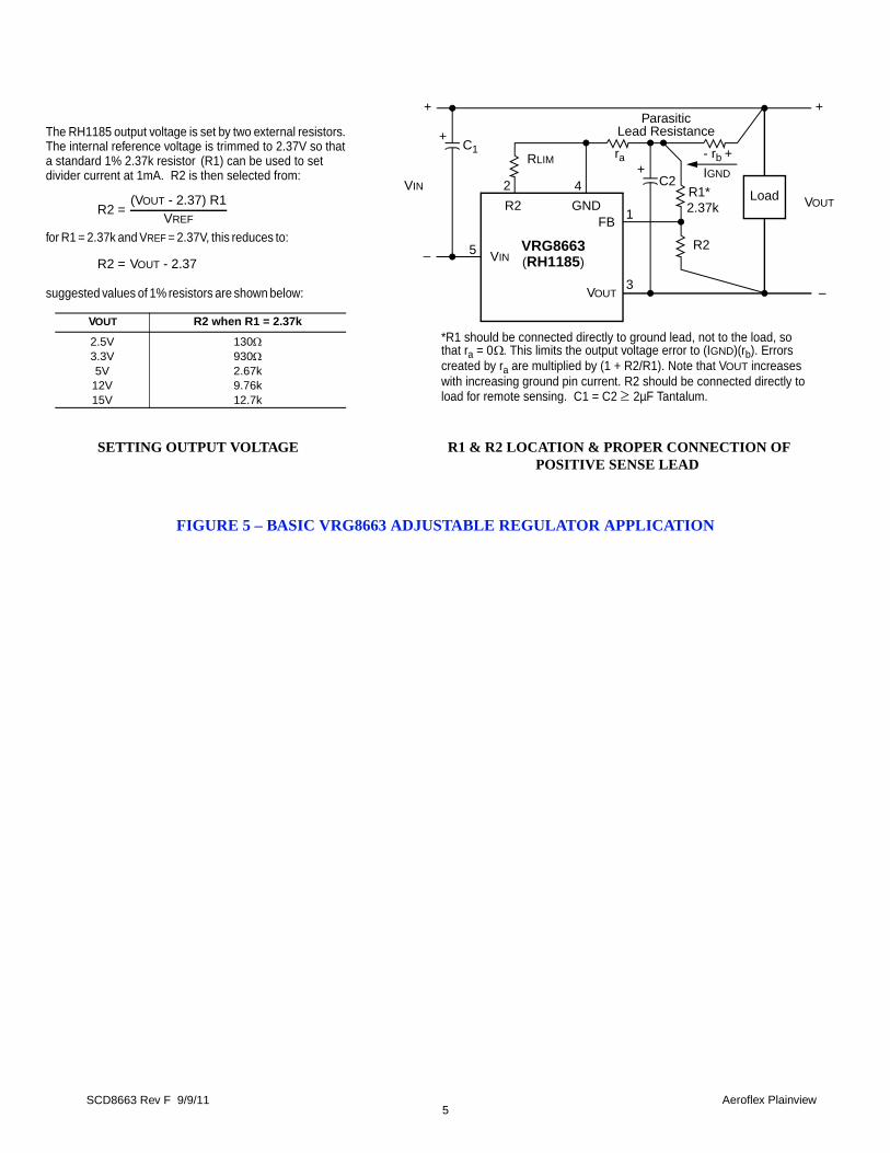
5SCD8663 Rev F 9/9/11 Aeroflex Plainview
FIGURE 5 – BASIC VRG8663 ADJUSTABLE REGULATOR APPLICATION
R1 & R2 LOCATION & PROPER CONNECTION OF POSITIVE SENSE LEAD
SETTING OUTPUT VOLTAGE
The RH1185 output voltage is set by two external resistors. The internal reference voltage is trimmed to 2.37V so that a standard 1% 2.37k resistor (R1) can be used to set divider current at 1mA. R2 is then selected from:
for R1 = 2.37k and VREF = 2.37V, this reduces to:
suggested values of 1% resistors are shown below:
R2 =(VOUT - 2.37) R1
VREF
R2 = VOUT - 2.37
VOUT R2 when R1 = 2.37k
2.5V 1303.3V 9305V 2.67k
12V 9.76k15V 12.7k
Parasitic
R2 GNDFB
VINVRG8663(RH1185)
VOUT
*R1 should be connected directly to ground lead, not to the load, so that ra = 0. This limits the output voltage error to (IGND)(rb). Errors created by ra are multiplied by (1 + R2/R1). Note that VOUT increases with increasing ground pin current. R2 should be connected directly to load for remote sensing. C1 = C2 2µF Tantalum.
VIN
C1
+
– 5
Lead Resistance
Load2 4
1
3
RLIM ra
R2
R1*2.37k
- rb +
IGND
+
+C2
VOUT
+
–

6SCD8663 Rev F 9/9/11 Aeroflex Plainview
FIGURE 6 – PACKAGE OUTLINE — SURFACE MOUNT
4X R.020
.550MAX
.301MAX
.127MAX
.0153 Places
.286
.005
.005
MIN.030
.030MIN
R.025 MAX6 Places
.095
.030 MIN
.005
.005
4 Places.120
.2005
.150
3 2
4 1
4 Places
PAD 1
NOTE 1. Package & Lid are electrically isolated from signal pads.

7SCD8663 Rev F 9/9/11
PLAINVIEW, NEW YORKToll Free: 800-THE-1553 Fax: 516-694-6715
SE AND MID-ATLANTIC Tel: 321-951-4164 Fax: 321-951-4254
INTERNATIONALTel: 805-778-9229Fax: 805-778-1980
WEST COAST Tel: 949-362-2260Fax: 949-362-2266
NORTHEASTTel: 603-888-3975Fax: 603-888-4585
CENTRALTel: 719-594-8017Fax: 719-594-8468
w w w . a e r o f l e x . c o m i n f o - a m s @ a e r o f l e x . c o m
Aeroflex Microelectronic Solutions reserves the right to change at any time without notice the specifications, design, function, or form of its products described herein. All parameters must be validated for each customer's application by engineering. No liability is assumed as a result of use of this product. No patent licenses are implied.
EXPORT CONTROL: EXPORT WARNING:This product is controlled for export under the International Traffic inArms Regulations (ITAR). A license from the U.S. Department ofState is required prior to the export of this product from the UnitedStates.
Aeroflex’s military and space products are controlled for export underthe International Traffic in Arms Regulations (ITAR) and may not besold or proposed or offered for sale to certain countries. (See ITAR126.1 for complete information.)
Our passion for performance is defined by threeattributes represented by these three icons:solution-minded, performance-driven and customer-focused
and the Linear Technology logo are registered trademarks and RH1185 are a copyright of Linear Technology Corporation.
ORDERING INFORMATION
MODEL DLA SMD # SCREENING PACKAGE
VRG8663-7 - Commercial Flow, +25°C testing only
SMD Power Pkg
VRG8663-S -Military Temperature, -55°C to +125°C
Screened in accordance with the individual Test Methodsof MIL-STD-883 for Space Applications
VRG8663-201-1S 5962-0920702KYCIn accordance with DLA SMD
VRG8663-201-2S 5962-0920702KYA

SCD8666 Rev C
Manufactured using Space Qualified RH3080 die Radiation performance
Total dose: 100 krads(Si), Dose rate = 50 - 300 rads(Si)/s Current Limit with Foldback and Over-temperature protection Output voltage adjustable: 0V to 36V Outputs may be paralleled for higher current Post Radiated Dropout voltage:
0.60V @ 1.0Amps 0.39V @ 0.5Amps
Output current: 1.0A Packaging – Hermetic Ceramic
Hermetic Surface Mount Power 5 Pads, .545"L x .296"W x .120"Ht Weight - 2.0 gm max
Designed for aerospace and high reliability space applications
Aeroflex Plainview’s Radiation Hardness Assurance Plan is DLA Certified to MIL-PRF-38534, Appendix G.
DESCRIPTIONThe Aeroflex Plainview VRG8666 consists of a Positive Adjustable (RH3080) ULDO voltage regulatorcapable of supplying 1.0Amps over the output voltage range as defined under recommended operatingconditions. The VRG8666 offers excellent line and load regulation specifications and ripple rejection.Dropout (VIN - VOUT) decreases at lower load currents. The VRG8666 serves a wide variety of applications including SCSI-2 Active Terminator, High EfficiencyLinear Regulators, Post Regulators for Switching Supplies, Constant Current Regulators, Battery Chargersand Microprocessor Supply.The VRG8666 has been specifically designed to meet exposure to radiation environments and is configuredfor an SMD power package. It is guaranteed operational from -55°C to +125°C. Available screened toMIL-STD-883, the VRG8666 is ideal for demanding military and space applications.
Radiation Tolerant
FIGURE 1 – BLOCK DIAGRAM / SCHEMATIC
January 10, 2012
www.aeroflex.com/voltreg
Standard Products
FEATURES
VRG8666 Voltage Regulator, 1.0 Amp, Positive Ultra Low Dropout (ULDO), Adjustable
1
IN
SET
OUT
3
5RH3080
Positive Regulator
2
4
SENSE
VCONTROL

2SCD8666 Rev C 1/10/12 Aeroflex Plainview
ABSOLUTE MAXIMUM RATINGS
Parameter Range Units
Input Voltage, VCONTROL (Voltages are Relative to VOUT) +40, -0.3 VDC
Output Short Circuit Duration Indefinite -
Lead temperature (soldering 10 Sec) 300 °C
Input Output Differential 26 VDC
Output Voltage +36 VDC
ESD 2000 1/ VOperating Junction Temperature Range -55 to +150 °CStorage Temperature Range -65 to +150 °C
Thermal Resistance (Junction to Case) JC 5 °C/W
1/ Meets ESD testing per MIL-STD-883, method 3015, Class 2.NOTICE: Stresses above those listed under "Absolute Maximums Rating" may cause permanent damage to the device. These are
stress rating only; functional operation beyond the "Operation Conditions" is not recommended and extended exposure beyond the "Operation Conditions" may effect device reliability.
RECOMMENDED OPERATING CONDITIONS
Parameter Range Units
Output Voltage Range 0 to 35 VDC
Input Output Differential 0.5 to 26 VDC
Case Operating Temperature Range -55 to +125 °C
Input Voltage (Voltages are Relative to VOUT) 1 to 36 V
VCONTROL (Voltages are Relative to VOUT) 2 to 36 V
ELECTRICAL PERFORMANCE CHARACTERISTICSUnless otherwise specified: -55°C < Tc < +125°C.
Parameter Symbol Conditions (P < PMAX) MIN MAX Units
Set Pin Current IREF1 1.0mA < ILOAD < 1.0A, 1.6V < (VIN - VOUT) < 25V 9.8 10.2 µA
Set Pin Current 1/, 3/ IREF2 VIN = 1V, VCONTROL = 2V, ILOAD = 1mA 9.8 10.2 µAOutput Offset Voltage(VOUT - VSET) VOS1 VIN = VCONTROL = 2V, ILOAD = 1mA -9.0 9.0 mV
Output Offset Voltage(VOUT - VSET) 1/, 3/ VOS2 VIN = 1V, VCONTROL = 2V, ILOAD = 1mA, -9.0 9.0 mV
Line Regulation 1/VOS
1V < VIN < 26V, 2V < VCONTROL < 26V,ILOAD = 1mA, TJ = +25C -0.15 0.15 mV/V
ISET 1V < VIN < 26V, 2V < VCONTROL < 26V, ILOAD = 1mA 4/ -0.9 0.9 nA/V
Load Regulation 1/VOS (VIN - VOUT) = 3V, ILOAD = 1mA to 0.1A -1.4 1.4 mVISET ILOAD = 1mA to 1A 4/ -25 25 nA
VCONTROL Dropout Voltage VCDROPILOAD = 1.0A - 1.60
VILOAD = 0.1A 1/, 3/ - 1.65
VIN Dropout Voltage VINDROPILOAD = 1.0A - 0.5
VILOAD = 0.1A 1/, 3/ - 0.3
Current Limit 1/, 3/ IMAX VIN = VCONTROL = +5V, VSET = 0V , VOUT = -0.1V 1.1 - AMinimum Load Current 1/ IMIN VIN = VCONTROL = 26V, VOUT = 0.1V - 1.0 mA
Ripple Rejection - ILOAD = 0.2A, (VIN - VOUT) = 3V, f = 120Hz, COUT = 2.2µF, CSET = 0.1µF 60 - dB
Thermal Regulation - 30ms pulse, TC = +25°C - 0.03 %/W
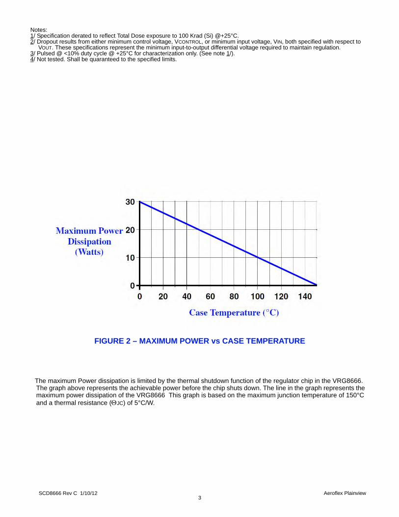
3SCD8666 Rev C 1/10/12 Aeroflex Plainview
The maximum Power dissipation is limited by the thermal shutdown function of the regulator chip in the VRG8666.
The graph above represents the achievable power before the chip shuts down. The line in the graph represents the maximum power dissipation of the VRG8666 This graph is based on the maximum junction temperature of 150°C and a thermal resistance (JC) of 5°C/W.
Notes:1/ Specification derated to reflect Total Dose exposure to 100 Krad (Si) @+25°C.2/ Dropout results from either minimum control voltage, VCONTROL, or minimum input voltage, VIN, both specified with respect to
VOUT. These specifications represent the minimum input-to-output differential voltage required to maintain regulation.3/ Pulsed @ <10% duty cycle @ +25°C for characterization only. (See note 1/).4/ Not tested. Shall be quaranteed to the specified limits.
FIGURE 2 – MAXIMUM POWER vs CASE TEMPERATURE

4SCD8666 Rev C 1/10/12 Aeroflex Plainview
FIGURE 4 – RH3080 TYPICAL DROPOUT FIGURE 3 – RH3080 CURRENT LIMIT
See Note 1, pg 2.
VOLTAGE CURVE
See Note 4, pg 2.
FIGURE 5 – BASIC VRG8666 ADJUSTABLE REGULATOR APPLICATION
Rset Vout10uA--------------=

5SCD8666 Rev C 1/10/12 Aeroflex Plainview
FIGURE 6 – PACKAGE OUTLINE — SURFACE MOUNT
NOTES:1. Package & Lid are electrically isolated from signal pads
4X R.020
.550MAX
.301MAX
.127MAX
.0153 Places
.286
.005
.005
MIN.030
.030MIN
R.025 MAX6 Places
.095
.030 MIN
.005
.005
4 Places.120
.2005
.150
3 2
4 1
4 PlacesPin 1 Epoxy Dot (on side)

6SCD8666 Rev C 1/10/12
PLAINVIEW, NEW YORKToll Free: 800-THE-1553 Fax: 516-694-6715
SE AND MID-ATLANTIC Tel: 321-951-4164 Fax: 321-951-4254
INTERNATIONALTel: 805-778-9229Fax: 805-778-1980
WEST COAST Tel: 949-362-2260Fax: 949-362-2266
NORTHEASTTel: 603-888-3975Fax: 603-888-4585
CENTRALTel: 719-594-8017Fax: 719-594-8468
w w w . a e r o f l e x . c o m i n f o - a m s @ a e r o f l e x . c o m
Aeroflex Microelectronic Solutions reserves the right to change at any time without notice the specifications, design, function, or form of its products described herein. All parameters must be validated for each customer's application by engineering. No liability is assumed as a result of use of this product. No patent licenses are implied.
EXPORT CONTROL: EXPORT WARNING:This product is controlled for export under the International Traffic inArms Regulations (ITAR). A license from the U.S. Department ofState is required prior to the export of this product from the UnitedStates.
Aeroflex’s military and space products are controlled for export underthe International Traffic in Arms Regulations (ITAR) and may not besold or proposed or offered for sale to certain countries. (See ITAR126.1 for complete information.)
Our passion for performance is defined by threeattributes represented by these three icons:solution-minded, performance-driven and customer-focused
LT, LTC, , Linear Technology and the Linear logo are registered trademarks and RH3080 is copyright Linear Technology Corporation.
For detailed performance characteristic curves, applications information and typical applications see the latest datasheets for their RH3080, which is available on-line at www.linear.com.
ORDERING INFORMATION
MODEL DLA SMD # SCREENING PACKAGE
VRG8666-7 - Commercial Flow, +25°C testing only
SMD Power Pkg
VRG8666-S -Military Temperature, -55°C to +125°C
Screened in accordance with the individual Test Methodsof MIL-STD-883 for Space Applications
VRG8666-201-1S 5962-1120502KYCDLA SMD Pending
VRG8666-201-2S 5962-1120502KYA
VRG8666-901-1S 5962R1120502KYCDLA SMD and Radiation Certification Pending
VRG8666-901-2S 5962R1120502KYA

SCD8684 Rev B
Manufactured using Space Qualified RH1084 die Radiation performance
- Total dose: 100 krads(Si), Dose rate = 50 - 300 rads(Si)/s Thermal shutdown Output voltage adjustable: 1.25V to 23V Dropout voltage: 1.80V at 3.0Amps 3-Terminal Output current: 3.0Amps Voltage reference: 1.25V +2%, -3.2% Load regulation: 0.35% max Line regulation: 0.25% max Ripple rejection: >60dB Packaging – Hermetic Ceramic
- SMD-0.5 Surface mount- 3 Pads, .400"L x .296"W x .120"Ht- Power package- Weight - 2 gm max
Designed for aerospace and high reliability space applications
Aeroflex Plainview’s Radiation Hardness Assurance Plan is DLA Certified to MIL-PRF-38534, Appendix G.
DESCRIPTIONThe Aeroflex Plainview VRG8684 consists of a Positive Adjustable (RH1084) LDO voltage regulator capable ofsupplying 3.0Amps over the output voltage range as defined under recommended operating conditions. The VRG8684offers excellent line and load regulation specifications and ripple rejection.
The VRG8684 serves a wide variety of applications including SCSI-2 Active Terminator, High Efficiency LinearRegulators, Post Regulators for Switching Supplies, Constant Current Regulators, Battery Chargers andMicroprocessor Supply.
The VRG8684 has been specifically designed to meet exposure to radiation environments and is configured for aSMD-0.5 SMT power package. It is guaranteed operational from -55°C to +125°C. Available screened in accordancewith MIL-PRF-38534, the VRG8684 is ideal for demanding military and space applications.
Dropout (VIN - VOUT) decreases at lower load currents.
Radiation Tolerant
FIGURE 1 – BLOCK DIAGRAM / SCHEMATIC
October 24, 2011
www.aeroflex.com/voltreg
Standard Products
FEATURES
VRG8684 Voltage Regulator, 3.0 Amp, PositiveLow Dropout (LDO), Adjustable
2
VIN
ADJ
VOUT
3
1
RH1084Positive
Regulator

2SCD8684 Rev B 10/24/11 Aeroflex Plainview
ABSOLUTE MAXIMUM RATINGS
PARAMETER RANGE UNITS
Input Voltage +25 VDC
Lead temperature (soldering 10 Sec) 300 °CInput Output Differential 25 VDC
Load Current, maximum 6.0 AOutput Voltage +25 VDC
ESD (MIL-STD-883, M3015, Class 2) 2000 to 3999 VOperating Junction Temperature Range -55 to +150 °CStorage Temperature Range -65 to +150 °CThermal Resistance (Junction to Case) JC 2 °C/W
NOTICE: Stresses above those listed under "Absolute Maximums Rating" may cause permanent damage to the device. These are stress rating only; functional operation beyond the "Operation Conditions" is not recommended and extended exposure beyond the "Operation Conditions" may effect device reliability.
RECOMMENDED OPERATING CONDITIONS
PARAMETER RANGE UNITS
Output Voltage Range 1.25 to 23 VDC
Input Output Differential 1.8 to 24 VDC
Case Operating Temperature Range -55 to +125 °C
ELECTRICAL PERFORMANCE CHARACTERISTICS 1/UNLESS OTHERWISE SPECIFIED: -55°CTC+125°C
PARAMETER SYM CONDITIONS (PPMAX) MIN MAX UNITS
Reference Voltage 3/, 2/ VREF 1.5V < (VIN - VOUT) < 15V, 10mA < IOUT < 3.0A 1.210 1.275 V
Dropout Voltage 4/, 2/ VDROP VREF = 1%, IOUT = 3.0A - 1.8 V
Line Regulation 3/, 2/ ILOAD = 10mA, 1.5V < (VIN - VOUT) < 15V - 0.25 %
Load Regulation 3/, 2/ 10mA < IOUT < 3.0A, (VIN - VOUT) = 3V - 0.35 %
Adjust Pin Current 2/ - 120 µAAdjust Pin Current Change 2/ 10 mA < IOUT < 3.0A, 1.5V < (VIN - VOUT) < 15V - 5 µA
Minimum Load Current 5/, 2/ IMIN (VIN - VOUT) = 25V - 10 mA
Current Limit 2/ ICL (VIN - VOUT) = 5V 5.25 A
Ripple Rejection 3/ IOUT = 3.0A, (VIN - VOUT) = 3V, f = 120Hz, CADJ = COUT = 25µF 60 - dB
Thermal Regulation 30ms pulse, TC = +25°C - 0.02 %/WVREF Long-Term Stability 5/ Burn In: TC = +125°C @ 1000hrs minimum, Tested at +25°C. - 1.0 %
Notes:1/ The manufacturer’s output current rating for the RH1084MK positive regulator integrated circuit is 5.0 Amps. For Compliance with
the Current Density specifictation of MIL-STD-883 Rev. C, the electrical performance characteristics are specified at an output current of 3.0 Amps.
2/ Specification derated to reflect total dose exposure to 100krads (Si) at +25°C.3/ Line and load regulation are guaranteed up to the maximum power dissipation of 15W. Power dissipation is determined by the
input/output differential voltage and the output current. Guaranteed maximum power dissipation will not be available over the full input/output voltage range.
4/ Dropout voltage is specified over the full output current range of the device.5/ Not tested. Shall be guaranteed by design, characterization, or correlation to other tested parameters.
VOUTVIN
VOUTIOUT

3SCD8684 Rev B 10/24/11 Aeroflex Plainview
FIGURE 3 – RH1084 DROPOUT VOLTAGE CURVE
FIGURE 2 – MAXIMUM POWER vs CASE TEMPERATURE
RH1084
The maximum Power dissipation is limited by the thermal shutdown function of the regulator chip in the VRG8684.The graph above represents the achievable power before the chip shuts down. The line in the graph represents themaximum power dissipation of the VRG8684 This graph is based on the maximum junction temperature of 150°Cand a thermal resistance (JC) of 2°C/W.
Case Temperature (Degrees C)
Max
imu
m P
ow
er D
issi
pat
ion
(Wat
ts)
VRG8684
See Note 1/ on page 2

4SCD8684 Rev B 10/24/11 Aeroflex Plainview
VRG8684VIN Vout
ADJ
R1
R2
VREF22µFTant.
IADJ = 55µAVREF = 1.25V,+Reg = VOUT = VREF (1+R2/R1) + (IADJ x R2)
FIGURE 5 – BASIC RH1084 ADJUSTABLE REGULATOR APPLICATION
2 1
3
FIGURE 4 – RH1084 SHORT CIRCUIT CURRENT
RH1084
10µFTant.
See Note 1/ on page 2

5SCD8684 Rev B 10/24/11 Aeroflex Plainview
1
2 3
FIGURE 6 – VRG8684 PACKAGE OUTLINE — SURFACE MOUNT
NOTE: Package & Lid are electrically isolated from signal pads.

6SCD8684 Rev B 10/24/11
PLAINVIEW, NEW YORKToll Free: 800-THE-1553 Fax: 516-694-6715
SE AND MID-ATLANTIC Tel: 321-951-4164 Fax: 321-951-4254
INTERNATIONALTel: 805-778-9229Fax: 805-778-1980
WEST COAST Tel: 949-362-2260Fax: 949-362-2266
NORTHEASTTel: 603-888-3975Fax: 603-888-4585
CENTRALTel: 719-594-8017Fax: 719-594-8468
w w w . a e r o f l e x . c o m i n f o - a m s @ a e r o f l e x . c o m
Aeroflex Microelectronic Solutions reserves the right to change at any time without notice the specifications, design, function, or form of its products described herein. All parameters must be validated for each customer's application by engineering. No liability is assumed as a result of use of this product. No patent licenses are implied.
EXPORT CONTROL: EXPORT WARNING:This product is controlled for export under the International Traffic inArms Regulations (ITAR). A license from the U.S. Department ofState is required prior to the export of this product from the UnitedStates.
Aeroflex’s military and space products are controlled for export underthe International Traffic in Arms Regulations (ITAR) and may not besold or proposed or offered for sale to certain countries. (See ITAR126.1 for complete information.)
LT, LTC, , Linear Technology and the Linear logo are registered trademarks and RH1084 is copyright Linear Technology Corporation.
For detailed performance characteristic curves, applications information and typical applications see the latest datasheet for their RH1084, which is available on-line at www.linear.com.
Our passion for performance is defined by threeattributes represented by these three icons:solution-minded, performance-driven and customer-focused
ORDERING INFORMATION
MODEL DLA SMD # SCREENING PACKAGE
VRG8684-7 - Commercial Flow, +25°C testing only
SMD-0.5Power Pkg
VRG8684-S -Military Temperature, -55°C to +125°C
Screened in accordance with the individual Test Methodsof MIL-STD-883 for Space Applications
VRG8684-201-1S 5962-0924501KXCDLA SMD Pending
VRG8684-201-2S 5962-0924501KXA

SCD8687 Rev B
Manufactured using Linear Technology Corporation ® Space Qualified RH1084 die Radiation performance
- Total dose > 100 krad (Si), Dose rate = 50 - 300 rads(Si)/s
Two-Independent voltage regulators Thermal shutdown Output voltage adjustable: 1.25V to 23V Dropout voltage: 1.80V at 3.0Amps 3-Terminal Output current: 3.0Amps Voltage reference: 1.25V +2%, -3.2% Load regulation: 0.35% max Line regulation: 0.25% max Ripple rejection: >60dB
Packaging – Hermetic metal- Thru-hole or Surface mount- 8 Leads, .755"L x .415"W x .200"Ht- Power package- Weight - 6 gm max
Designed for aerospace and high reliability space applications
DESCRIPTIONThe Aeroflex Plainview VRG8687/8688 consists of two Positive Adjustable (RH1084) LDO voltage regulators eachcapable of supplying 3.0Amps over the output voltage range as defined under recommended operating conditions. TheVRG8687/8688 offers excellent line and load regulation specifications and ripple rejection. There is full electricalisolation between the regulators and each regulator to the package.Dropout (VIN - VOUT) decreases at lower load currents for both regulators. The VRG8687/8688 serves a wide variety of applications including SCSI-2 Active Terminator, High EfficiencyLinear Regulators, Post Regulators for Switching Supplies, Constant Current Regulators, Battery Chargers andMicroprocessor Supply.The VRG8687/8688 has been specifically designed to meet exposure to radiation environments. The VRG8687 isconfigured for a Thru-Hole 8 lead metal power package and the VRG8688 is configured for a Surface Mount 8 leadmetal power package. It is guaranteed operational from -55°C to +125°C. Available screened in accordance withMIL-PRF-38534, the VRG8687/8688 is ideal for demanding military and space applications. For detailed performance characteristic curves, applications information and typical applications see thelatest Linear Technology Corporation ® data sheets for their RH/LT1084, which is available on-line atwww.linear.com.
Radiation Tolerant
FIGURE 1 – BLOCK DIAGRAM / SCHEMATIC
October 24, 2011
www.aeroflex.com/voltreg
Standard Products
FEATURES
VRG8687/VRG8688Dual Voltage Regulator, 3.0 Amp, Positive
4
VIN_2
ADJ_2
VOUT_2
5
8
VIN_1
ADJ_1
VOUT_1
1
2 6RH1084Positive
Regulator
RH1084Positive
Regulator
Low Dropout (LDO), Adjustable
3 7SENSE_2SENSE_1
Aeroflex Plainview’s Radiation Hardness Assurance Plan is DLA Certified to MIL-PRF-38534, Appendix G.

2SCD8687 Rev B 10/24/11 Aeroflex Plainview
ABSOLUTE MAXIMUM RATINGS
Parameter Range Units
Input Voltage +25 VDC
Lead temperature (soldering 10 Sec) 300 °CInput Output Differential 25 VDC
Load Current, maximum 6.0 AOutput Voltage +25 VDC
ESD (MIL-STD-883, M3015, Class 2) 2000 to 3999 VOperating Junction Temperature Range -55 to +150 °CStorage Temperature Range -65 to +150 °C
Thermal Resistance, Junction to case JC 5 °C/W
NOTICE: Stresses above those listed under "Absolute Maximums Rating" may cause permanent damage to the device. These are stress rating only; functional operation beyond the "Operation Conditions" is not recommended and extended exposure beyond the "Operation Conditions" may effect device reliability.
RECOMMENDED OPERATING CONDITIONS
Parameter Range Units
Output Voltage Range 1.25 to 23 VDC
Input Output Differential 3/ 1.8 to 24 VDC
Case Operating Temperature Range -55 to +125 °C
ELECTRICAL PERFORMANCE CHARACTERISTICS 1/UNLESS OTHERWISE SPECIFIED: -55°C TC +125°C
Parameter Symbol Conditions (PPMAX) Min Max Units
Reference Voltage 3/, 2/ VREF 1.5V < (VIN - VOUT) < 15V, 10mA < IOUT < 3.0A 1.210 1.275 V
Line Regulation 3/, 2/ ILOAD = 10mA, 1.5V < (VIN - VOUT) < 15V - 0.25 %
Load Regulation 3/, 2/ 10mA < IOUT < 3.0A, (VIN - VOUT) = 3V - 0.35 %
Dropout Voltage 4/, 2/ VDROP VREF = 1%, IOUT = 3.0A - 1.8 V
Adjust Pin Current 2/ - - 120 µA
Adjust Pin Current Change 2/ - 10 mA < IOUT < 3.0A, 1.5V < (VIN - VOUT) < 15V - 5 µA
Minimum Load Current 5/, 2/ IMIN (VIN - VOUT) = 25V - 10 mA
Current Limit 2/ ICL (VIN - VOUT) = 5V 5.25 - A
Ripple Rejection 3/ - IOUT = 3.0A, (VIN - VOUT) = 3V, f = 120Hz, CADJ = COUT = 25µF 60 - dB
Thermal Regulation - 30ms pulse, TC = +25°C - 0.015 %/W
VREF Long-Term Stability 5/ - Burn In: TC = +125°C @ 1000hrs minimum, tested @ 25°C - 1.0 %Notes:1/ The manufacturer’s output current rating for the RH1084MK positive regulator integrated circuit is 5.0 Amps. For Compliance with the
Current Density specifictation of MIL-STD-883 Rev. C, the electrical performance characteristics are specified at an output current of 3.0 Amps.
2/ Specification derated to reflect total dose exposure to 100krads (Si) at +25°C.3/ Line and load regulation are guaranteed up to the maximum power dissipation of 15W per device. Power dissipation is determined by
the input/output differential voltage and the output current. Guaranteed maximum power dissipation will not be available over the full input/output voltage range.
4/ Dropout voltage is specified over the full output current range of the device. 5/ Not tested. Shall be guaranteed by design, characterization, or correlation to other tested parameters.
VOUTVIN
VOUTIOUT

3SCD8687 Rev B 10/24/11 Aeroflex Plainview
FIGURE 3 – RH1084 SHORT CIRCUIT CURRENT
The maximum Power dissipation is limited by the thermal shutdown function of each regulator chip in theVG8687/8688. The graph above represents the achievable power before the chip shuts down. The first line in thegraph represents the maximum power dissipation of the VG8687/8688 with one regulator on (the other off) and theother line represents both regulators on dissipating equal power. If both regulators are on and one regulator isdissipating more power that the other, the maximum power dissipation of the VG8687/8688 will fall between the twolines. This graph is based on the maximum junction temperature of 150°C and a thermal resistance (JC) of 5°C/W.
60
50
40
30
20
10
0 20 40 60 80 100 120 140
Case Temperature (°C)
1 Regulator
0
Both RegulatorsMaximum Power
Dissipation(Watts)
FIGURE 2 – MAXIMUM POWER vs CASE TEMPERATURE
See Note 1/ on page 2
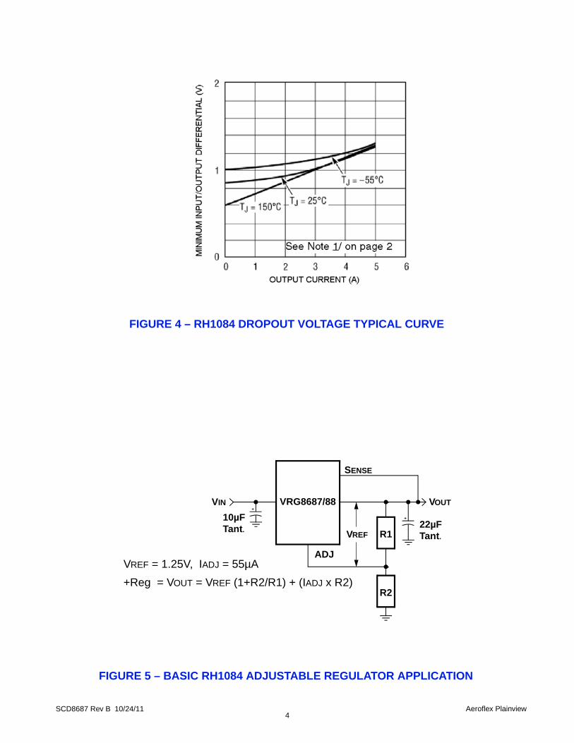
4SCD8687 Rev B 10/24/11 Aeroflex Plainview
VRG8687/88VIN VOUT
ADJ
R1
R2
VREF22µFTant.
IADJ = 55µAVREF = 1.25V,+Reg = VOUT = VREF (1+R2/R1) + (IADJ x R2)
FIGURE 5 – BASIC RH1084 ADJUSTABLE REGULATOR APPLICATION
SENSE
10µFTant.
FIGURE 4 – RH1084 DROPOUT VOLTAGE TYPICAL CURVE

5SCD8687 Rev B 10/24/11 Aeroflex Plainview
FIGURE 5 – VRG8687 PACKAGE OUTLINE — THRU-HOLE POWER PACKAGE
TABLE I – PIN NUMBERS vs FUNCTION
PIN FUNCTION
1 ADJ_1
2 VOUT_1
3 SENSE_1
4 VIN_2
5 ADJ_2
6 VOUT_2
7 SENSE_2
8 VIN_1
ø.145 THRU
.415.2075
R.065 TYP.4 PLCS
±.003
.220 MAX.
±.005
.040
±.002.030 DIA.
.150 REF. 2° MAX. TYP.
±.020.720MEASURED
LEAD TIP
IDENT
–A–
–C–
ø.010 B C A
Mø.010 C B A
2x .028
Mø.010 C B A
.230 MIN
.122
MAX.
.108
.300
.100
.755
.515
ESD/PIN 1
–B–
4
567
32
8
1
.632
.0908X
Notes: 1. Dimension Tolerance: ±.005 inches2. Package contains BeO substrate3. Case electrically isolated

6SCD8687 Rev B 10/24/11 Aeroflex Plainview
FIGURE 6 – VRG8688 PACKAGE OUTLINE — SURFACE MOUNT POWER PACKAGE
Notes: 1. Dimension Tolerance: ±.005 inches2. Package contains BeO substrate
TABLE II – PIN NUMBERS vs FUNCTION
PIN FUNCTION
1 ADJ_1
2 VOUT_1
3 SENSE_1
4 VIN_2
5 ADJ_2
6 VOUT_2
7 SENSE_2
8 VIN_1
3. Case electrically isolated
.108
.300
.100
ø.145 THRU
.415.2075
R.065 TYP.4 PLCS
.755
.515
±.003
.220 MAX.
±.005
.040±.002.030 DIA.
.122
.150 REF.
±.020.886
IDENTESD/PIN 1
–B–
–A–
–C–
ø.010 B C A
Mø.010 C B A
4
567
32
2x .028
Mø.010 C B A.020±.005
.060 ±.005
MAX. 8
1
.632
.0908X

7
PLAINVIEW, NEW YORKToll Free: 800-THE-1553 Fax: 516-694-6715
SE AND MID-ATLANTIC Tel: 321-951-4164 Fax: 321-951-4254
INTERNATIONALTel: 805-778-9229Fax: 805-778-1980
WEST COAST Tel: 949-362-2260Fax: 949-362-2266
NORTHEASTTel: 603-888-3975Fax: 603-888-4585
CENTRALTel: 719-594-8017Fax: 719-594-8468
w w w . a e r o f l e x . c o m i n f o - a m s @ a e r o f l e x . c o m
Aeroflex Microelectronic Solutions reserves the right to change at any time without notice the specifications, design, function, or form of its products described herein. All parameters must be validated for each customer's application by engineering. No liability is assumed as a result of use of this product. No patent licenses are implied.
EXPORT CONTROL: EXPORT WARNING:This product is controlled for export under the International Traffic inArms Regulations (ITAR). A license from the U.S. Department ofState is required prior to the export of this product from the UnitedStates.
Aeroflex’s military and space products are controlled for export underthe International Traffic in Arms Regulations (ITAR) and may not besold or proposed or offered for sale to certain countries. (See ITAR126.1 for complete information.)
SCD8687 Rev B 10/24/11
Our passion for performance is defined by threeattributes represented by these three icons:solution-minded, performance-driven and customer-focused
and the Linear Technology logo are registered trademarks and RH1084 are a copyright of Linear Technology Corporation.
ORDERING INFORMATION
MODEL DLA SMD # SCREENING PACKAGE
VRG8687-7 - Commercial Flow, +25°C testing only
8 LeadThru-HolePower Pkg
VRG8687-S -Military Temperature, -55°C to +125°C
Screened in accordance with the individual Test Methodsof MIL-STD-883 for Space Applications
VRG8687-201-1S 5962-1021302KUCDLA SMD Pending
VRG8687-201-2S 5962-1021302KUA
VRG8688-7 - Commercial Flow, +25°C testing only
8 LeadSurface Mount
Power Pkg
VRG8688-S -Military Temperature, -55°C to +125°C
Screened in accordance with the individual Test Methodsof MIL-STD-883 for Space Applications
VRG8688-201-1S 5962-1021302KZCDLA SMD Pending
VRG8688-201-2S 5962-1021302KZA

SCD8691 Rev F
11
12
10
Radiation performance- Total dose: 100 krads(Si),
Dose rate = 50 - 300 rads(Si)/s Output voltage adjustable: 1.0V to 3.3V Output current: 7.5A Dropout voltage: 0.5V at 7.5Amps Voltage reference: 1.0V ±0.5% Load regulation: 0.5% max Line regulation: 0.2% max Ripple rejection: >80dB
Enable Input - TTL / CMOS Compatible Slow Start capability Stable with multiple ceramic output capacitors Packaging – Hermetic metal
- Thru-hole or Surface mount- 12 Leads, 0.900"L x 1.000"W x .205"Ht- Power package- Weight - 18 gm max
Designed for aerospace and high reliability space applications
DESCRIPTIONThe Aeroflex Plainview VRG8691/92 is capable of supplying in excess of 7.5Amps over the output voltage range asdefined under recommended operating conditions. The regulator is exceptionally easy to set-up, requiring only 2external resistors to set the output voltage. The module design has been optimized for excellent regulation and lowdrop-out voltage. Figures 2 through 5 illustrate setting output voltage, setting current limits and choosing a slow startcapacitor. The VRG8691/92 serves a wide variety of applications including local on-card regulation, programmableoutput voltage regulation or precision current regulation.
The VRG8691/92 has been specifically designed to meet exposure to radiation environments. The VRG8691 isconfigured for a Thru-Hole 12 lead metal power package and the VRG8692 is configured for a Surface Mount 12 leadmetal power package. It is guaranteed operational from -55°C to +125°C. Available screened to MIL-STD-883, theVRG8691/92 is ideal for demanding military and space applications.
CURRENT LIMIT (ICL)The VRG8691/92 features internal current limiting making them virtually blowout-proof against overloads. The limitis nominally 11.5A @ Vin = 5V (see Table 2), but may be increased or decreased with the addition of one externalresistor (see Application Note 2). When the load current exceeds the ICL setting, the output of the VRG8691/92 willbe latched in an OFF state. To reset the latch condition, the ENABLE function (pin 5) can be cycled, enabled -disabled - enabled, or the VBIAS may be cycled ON - OFF - ON (if the Figure 5 configuration is being utilized).
VRG8691/92
Radiation Tolerant
FIGURE 1 – BLOCK DIAGRAM / SCHEMATIC
September 9, 2011
www.aeroflex.com/voltreg
Standard Products
Adjustable 7.5A Positive LDO Regulator
FEATURES
8
VRG8691/929
6
5
4
VOUT
VSENSE
Current Limit
GND
ENABLE
VBIAS
VIN
7 Slow Start
2
1
3
Aeroflex Plainview’s Radiation Hardness Assurance Plan is DLA Certified to MIL-PRF-38534, Appendix G.

2SCD8691 Rev F 9/9/11 Aeroflex Plainview
ABSOLUTE MAXIMUM RATINGS
PARAMETER RANGE UNITS
Operating (Junction) Temperature Range -55 to +150 °C
Lead Temperature (soldering, 10 sec) 300 °C
Storage Temperature Range -65 to +150 °C
VBIAS, VIN 7 V
Thermal Resistance (Junction to case JC) 1 °C/W
Power 25 1/ W
1/ Based on pass transistor limitations of (VIN - VO) x IO and JC < 1°C/W with 25°C max TJ rise and TC = +125°C.
NOTICE: Stresses above those listed under “Absolute Maximum Ratings” may cause permanent damage to the device. These are stress ratings only; functional operation beyond the “Operation Conditions” is not recommended and extended exposure beyond the “Operation Conditions” may effect device reliability.
RECOMMENDED OPERATING CONDITIONS
PARAMETER RANGE UNITS
Output Voltage Range 1.0 to 3.3 VDC
Case Operating Temperature Range -55 to +125 °C
Output Current 0 to 7.5 A
VBIAS 3.3 to 5.5 1/ VDC
VIN 1.8 to 5.5 2/ VDC
1/ VBIAS must maintain a level equal or above VIN but not fall below 3.3V2/ Depending upon VOUT setting.
ELECTRICAL PERFORMANCE CHARACTERISTICS 1/
PARAMETER SYM CONDITIONS MIN MAX UNITS
Reference Voltage VREF VIN = VBIAS = 5V, ENABLE = 0, 0A < IOUT < 7.5A 0.995 1.005 V
Line Regulation2V < VIN < 3V, VOUT = 1.0V, CIN > 47µF,
4.3V < VIN < 5.3V, VOUT = 3.3V, COUT > 47µF,- 0.2 %/V
Load Regulation 0A < IOUT < 7.5A, CIN > 47µF, COUT > 47µF, - 0.5 %
Ripple Rejection Ratio f = 120Hz, CLOAD = 47µF, VIN + VRIP > VOUT + VDROP(MAX) @ 5A,VIN = 4.3V, VRIP = 1VP-P, VOUT = 3.3V
80 - dB
Dropout Voltage VDROP @VOUT = 1%, 0A < IOUT < 7.5A - 0.5 V
Adjustment Pin Current IADJ - 3 µA
Minimum Load Current IMIN - 0 mA
Current Limit 2/ ICL 9.5 13.5 A
Long Term Stability 3/ - 1 %
Supply Current (VBIAS) IBIAS - 15 mANotes:1/ Unless otherwise specified, these specifications apply for post radiation: VBIAS = VIN = 5V, VOUT = 3.3V, IOUT = 7.5A and -55°C < Tc <+125°C, Min
Input/Output capacity of 47µF Tant with 1µF ceramic in parallel.2/ Current Limit is adjustable as shown in Application Note 2, Figures 3 and 4.3/ Not tested. Shall be guaranteed to the specified limits after 1000hr life test.
VOUTVIN
VOUTIOUT
VOUTTIME
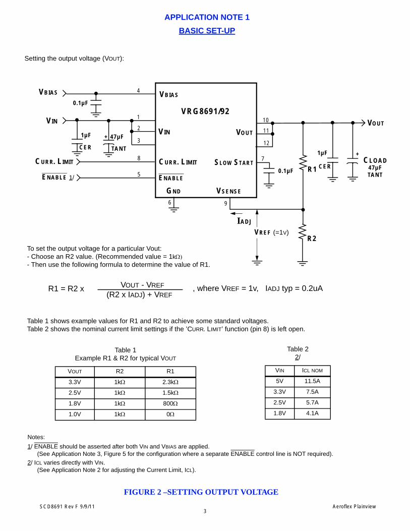
3SCD8691 Rev F 9/9/11 Aeroflex Plainview
VRG8691/92
VIN VOUT
VSENSE
R1
R2 VREF (=1V)
CURR. LIMIT
10
11
12
4
3
2
1
8
ENABLE
6 9
IADJ
7
5
0.1µF
47µF+
VBIAS
SLOW START
VBIAS
VIN
CURR. LIMIT
GND
0.1µF
FIGURE 2 –SETTING OUTPUT VOLTAGE
ENABLE 1/
Notes:1/ ENABLE should be asserted after both VIN and VBIAS are applied.
(See Application Note 3, Figure 5 for the configuration where a separate ENABLE control line is NOT required).2/ ICL varies directly with VIN.
(See Application Note 2 for adjusting the Current Limit, ICL).
To set the output voltage for a particular Vout: - Choose an R2 value. (Recommended value = 1k- Then use the following formula to determine the value of R1.
Table 1 shows example values for R1 and R2 to achieve some standard voltages.Table 2 shows the nominal current limit settings if the ’CURR. LIMIT’ function (pin 8) is left open.
CLOAD47µF
VOUT
+
Table 22/
VIN ICL NOM
5V 11.5A
3.3V 7.5A
2.5V 5.7A
1.8V 4.1A
Table 1Example R1 & R2 for typical VOUT
VOUT R2 R1
3.3V 1k 2.3k
2.5V 1k 1.5k
1.8V 1k 800
1.0V 1k 0
APPLICATION NOTE 1
BASIC SET-UP
Setting the output voltage (VOUT):
VOUT - VREF(R2 x IADJ) + VREF
R1 = R2 x , where VREF = 1v, IADJ typ = 0.2uA
1µF
TANT
1µFTANTCER
CER

4SCD8691 Rev F 9/9/11 Aeroflex Plainview
VRG8691/92
VIN VOUT
VSENSE CURR. LIMIT
RINC
10
11
12
4
3
2
1
8
ENABLE
6 9
75
0.1µF
47µF+
VBIAS
SLOW START
VBIAS
VIN
GND
0.1µF
FIGURE 3 – INCREASING THE CURRENT LIMIT (ICL)
ENABLE
- If the ’CURR. LIMIT’ function (pin 8) is left open, the ICL decreases from 11.5 A(NOM) as VIN is decreased from 5V (Table 3).
- To increase the current limit above the nominal setting for any VIN and ICL combination, use the following formula:
- To maintain ICL at the 11.5 A setting, for commonly found VIN voltages, apply RINC value found in Table 4.
Table 3
VIN RINC ICL NOM
5V Open 11.5 A
3.3V Open 7.5 A
2.5V Open 5.7 A
1.8V Open 4.1 A
Table 4
VIN RINC ICL NOM
5V Open 11.5 A
3.3V 56k 11.5 A
2.5V 30k 11.5 A
1.8V 16k 11.5 A
APPLICATION NOTE 2
SETTING THE CURRENT LIMIT
To Increase the Current Limit (ICL):
RINC(K-OHMS) = 30 x VIN30 x ICL
69- VIN( )
R1
R2 VREF (=1V)
IADJ
CLOAD47µF
VOUT
+
TANT
1µF
1µF
TANTCER
CER

5SCD8691 Rev F 9/9/11 Aeroflex Plainview
VRG8691/92
VIN VOUT
VSENSE
CURR. LIMIT
10
11
12
4
3
2
1
8
ENABLE
6 9
7
5
0.1µF
47µF+
VBIAS
SLOW START
VBIAS
VIN
CURR. LIMIT
GND
0.1µFENABLE
- As shown in Table 3, if the ’CURR. LIMIT’ function (pin 8) is left open, the ICL decreases from 11.5 A(NOM) as VIN is decreased from 5V.
- To achieve any ICL, less than nominal, use RDEC which can be calculated using the following formula:
RDEC
FIGURE 4 – DECREASING THE CURRENT LIMIT (ICL)
APPLICATION NOTE 2 (CONTINUED)
SETTING THE CURRENT LIMIT
To Decrease the Current Limit (ICL):
RDEC(K-OHMS) = 31 x VIN69 x VIN
30- ICL( )
R1
R2 VREF (=1V)
IADJ
CLOAD47µF
VOUT
+
TANT
1µF
1µF
TANTCER
CER

6SCD8691 Rev F 9/9/11 Aeroflex Plainview
VRG8691/92
VIN VOUT
VSENSE
CURR. LIMIT
10
11
12
4
3
2
1
8
ENABLE
6 9
7
5
0.1µF
47µF+
VBIAS
SLOW START
VBIAS
VIN
GND
0.1µF
CDELAY+
FIGURE 5 – DELAYED ENABLE
+++
APPLICATION NOTE 3
START UP SEQUENCE
Recommended Power Supply Sequencing Options:
- OPTION 1: Controlling the ENABLE line with a Digital signal (TTL / CMOS compatible).- Prior to applying power, disable the regulator by setting the ENABLE control line to a HIGH state.- Apply VIN and VBIAS. 1/- Wait until both VIN and VBIAS supplies have reached their operating levels.- Toggle the ENABLE control line to a LOW state to turn on VOUT of the regulator.
- OPTION 2: Controlling the ENABLE line using the CDELAY feature.- Connect a CDELAY capacitor between VBIAS and the ENABLE as shown in Figure 5 below. 2/- Apply VIN and VBIAS. 1/- CDELAY causes the regulator to self-enable after VBIAS has reached operating level.
NOTE: The ENABLE should always be asserted AFTER VIN and VBIAS have reached operating level.
NOTES:1/ VIN should be applied before VBIAS if the Slow Start feature is used.2/ CDELAY capacitor of 10uF is adequate for VBIAS rise times of up to 50ms.
1/
2/
R1
R2 VREF (=1V)
IADJ
CLOAD47µF
VOUT
+
TANT
1µF
1µF
TANTCER
CER

7SCD8691 Rev F 9/9/11 Aeroflex Plainview
FIGURE 6 – SLOW START
VRG8691/92
VIN VOUT
VSENSE
CURR. LIMIT
10
11
12
4
3
2
1
8
ENABLE
6 9
7
5
0.1µF
47µF+
VBIAS
SLOW START
VBIAS
VIN
GND
0.1µF
0 CSS+ENABLE
If it is desirable to control the output rise time, a capacitor (CSS) can be asserted on the Slow Start pin to adjust the rise time for the following:
A. Large load capacitance will cause high surge currents which will trip the current limit circuitry. The use of CSS will allow the output voltage to rise slowly thus mitigate the surge current phenomenon.
B. CSS may be used solely to control VOUT RISE TIME (Tr), when CLOAD is not an issue.
C. CSS is effective only when VIN is applied prior to VBIAS or ENABLE.
>CSSCLOAD
0.4 X VBIAS1300XVOUT NOM
ICL - ILOAD NOM
Note: CSS in Farads and TR in seconds.TR = VBIASVBIAS - 2.5( )CSS X 1300 X LN
APPLICATION NOTE 4
VOUT START UP RISE TIME CONTROL
Utilizing the Slow Start option:
When the VRG8691/92 is first powered up, using the Slow Start function controls the rate at which VOUT rises to the required voltage set by R1 and R2.
Note: VIN should be applied before VBIAS when the Slow Start feature is used.
R1
R2 VREF (=1V)
IADJ
CLOAD47µF
VOUT
+
TANT
1µF
1µF
TANT
CER
CER
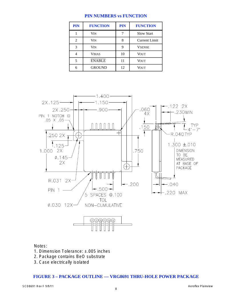
8SCD8691 Rev F 9/9/11 Aeroflex Plainview
FIGURE 3 – PACKAGE OUTLINE — VRG8691 THRU-HOLE POWER PACKAGE
PIN NUMBERS vs FUNCTION
PIN FUNCTION PIN FUNCTION
1 VIN 7 Slow Start
2 VIN 8 Current Limit
3 VIN 9 VSENSE
4 VBIAS 10 VOUT
5 ENABLE 11 VOUT
6 GROUND 12 VOUT
Notes: 1. Dimension Tolerance: ±.005 inches2. Package contains BeO substrate3. Case electrically isolated

9SCD8691 Rev F 9/9/11 Aeroflex Plainview
Notes:
FIGURE 4 – PACKAGE OUTLINE — VRG8692 SURFACE MOUNT POWER PACKAGE
1. Dimension Tolerance: ±.005 inches2. Package contains BeO substrate3. Case electrically isolated
PIN NUMBERS vs FUNCTION
PIN FUNCTION PIN FUNCTION
1 VIN 7 Slow Start
2 VIN 8 Current Limit
3 VIN 9 VSENSE
4 VBIAS 10 VOUT
5 ENABLE 11 VOUT
6 GROUND 12 VOUT

10SCD8691 Rev F 9/9/11
PLAINVIEW, NEW YORKToll Free: 800-THE-1553 Fax: 516-694-6715
SE AND MID-ATLANTIC Tel: 321-951-4164 Fax: 321-951-4254
INTERNATIONALTel: 805-778-9229Fax: 805-778-1980
WEST COAST Tel: 949-362-2260Fax: 949-362-2266
NORTHEASTTel: 603-888-3975Fax: 603-888-4585
CENTRALTel: 719-594-8017Fax: 719-594-8468
w w w . a e r o f l e x . c o m i n f o - a m s @ a e r o f l e x . c o m
Aeroflex Microelectronic Solutions reserves the right to change at any time without notice the specifications, design, function, or form of its products described herein. All parameters must be validated for each customer's application by engineering. No liability is assumed as a result of use of this product. No patent licenses are implied.
Our passion for performance is defined by threeattributes represented by these three icons:solution-minded, performance-driven and customer-focused
EXPORT CONTROL: EXPORT WARNING:This product is controlled for export under the International Traffic inArms Regulations (ITAR). A license from the U.S. Department ofState is required prior to the export of this product from the UnitedStates.
Aeroflex’s military and space products are controlled for export underthe International Traffic in Arms Regulations (ITAR) and may not besold or proposed or offered for sale to certain countries. (See ITAR126.1 for complete information.)
ORDERING INFORMATION
MODEL DLA SMD # SCREENING PACKAGE
VRG8691-7 - Commercial Flow, +25°C testing only
12 LeadThru-HolePower Pkg
VRG8691-S -Military Temperature, -55°C to +125°C
Screened in accordance with the individual Test Methodsof MIL-STD-883 for Space Applications
VRG8691-201-1S 5962-0923701KXCDLA SMD Pending
VRG8691-201-2S 5962-0923701KXA
VRG8692-7 - Commercial Flow, +25°C testing only
12 LeadSurface Mount
Power Pkg
VRG8692-S -Military Temperature, -55°C to +125°C
Screened in accordance with the individual Test Methodsof MIL-STD-883 for Space Applications
VRG8692-201-1S 5962-0923701KYCDLA SMD Pending
VRG8692-201-2S 5962-0923701KYA

REVISIONS
LTR DESCRIPTION DATE (YR-MO-DA) APPROVED
A Added device type 03 and 04. Paragraph 1.4 changed the output voltage , negative voltage regulator for device type 01 from -1.2 V to -22 V dc to -1.2 V to -27 V dc. Table I; corrected the limit for the current limit test IMAX, should be specified as a min limit. -sld
07-11-28
Robert M. Heber
B
Sheet 5; made changes to the thermal regulation and current limit tests. Sheet 6; made changes to the thermal regulation, adjustment pin current change, and the minimum load current tests. Sheet 7; made changes to the current limit and long term stability tests. -sld
08-08-11
Robert M. Heber
C
Corrected Figure 1 to show the pin configuration without the ceramic seal accross all pins but only to show the seal on each pin individually. Figure 1 corrected the dimensions R and S1, removed the dimension D2 for case outline X. -sld
08-10-23
Robert M. Heber
REV
SHEET
REV C C
SHEET 15 16
REV STATUS REV C C C C C C C C C C C C C C OF SHEETS SHEET 1 2 3 4 5 6 7 8 9 10 11 12 13 14
PMIC N/A PREPARED BY Steve Duncan
DEFENSE SUPPLY CENTER COLUMBUS
STANDARD MICROCIRCUIT
DRAWING
CHECKED BY Greg Cecil
COLUMBUS, OHIO 43218-3990 http://www.dscc.dla.mil/
APPROVED BY Robert M. Heber
MICROCIRCUIT, HYBRID, DUAL VOLTAGE REGULATOR, POSTIVE AND NEGATIVE, ADJUSTABLE
THIS DRAWING IS AVAILABLE
FOR USE BY ALL DEPARTMENTS
AND AGENCIES OF THE DEPARTMENT OF DEFENSE
DRAWING APPROVAL DATE 07-04-25
AMSC N/A
REVISION LEVEL C
SIZE A
CAGE CODE 67268
5962-05219
SHEET 1 OF
16
DSCC FORM 2233 APR 97 5962-E020-09

STANDARD MICROCIRCUIT DRAWING
SIZE
A
5962-05219
DEFENSE SUPPLY CENTER COLUMBUS
COLUMBUS, OHIO 43218-3990
REVISION LEVEL C
SHEET 2
DSCC FORM 2234 APR 97
1. SCOPE
1.1 Scope. This drawing documents five product assurance classes as defined in paragraph 1.2.3 and MIL-PRF-38534. A choice of case outlines and lead finishes which are available and are reflected in the Part or Identifying Number (PIN). When available, a choice of radiation hardness assurance levels are reflected in the PIN.
1.2 PIN. The PIN shall be as shown in the following example:
5962 - 05219 01 K X X
Federal RHA Device Device Case Lead stock class designator type class outline finish designator (see 1.2.1) (see 1.2.2) designator (see 1.2.4) (see 1.2.5)
\ / (see 1.2.3) \/ Drawing number
1.2.1 Radiation hardness assurance (RHA) designator. RHA marked devices shall meet the MIL-PRF-38534 specified RHA
levels and shall be marked with the appropriate RHA designator. A dash (-) indicates a non-RHA device.
1.2.2 Device type(s). The device type(s) identify the circuit function as follows:
Device type Generic number Circuit function
01 8601, 8602 Dual voltage regulator, positive and negative, adjustable 02 8603, 8604 Dual voltage regulator, positive and negative, adjustable 03 8607, 8608 Dual voltage regulator, positive, adjustable 04 8609, 8610 Dual voltage regulator, negative, adjustable
1.2.3 Device class designator. This device class designator shall be a single letter identifying the product assurance level. All levels are defined by the requirements of MIL-PRF-38534 and require QML Certification as well as qualification (Class H, K, and E) or QML Listing (Class G and D). The product assurance levels are as follows:
Device class Device performance documentation
K Highest reliability class available. This level is intended for use in space applications. H Standard military quality class level. This level is intended for use in applications
where non-space high reliability devices are required. G Reduced testing version of the standard military quality class. This level uses the
Class H screening and In-Process Inspections with a possible limited temperature range, manufacturer specified incoming flow, and the manufacturer guarantees (but may not test) periodic and conformance inspections (Group A, B, C and D).
E Designates devices which are based upon one of the other classes (K, H, or G)
with exception(s) taken to the requirements of that class. These exception(s) must be specified in the device acquisition document; therefore the acquisition document should be reviewed to ensure that the exception(s) taken will not adversely affect system performance.
D Manufacturer specified quality class. Quality level is defined by the manufacturers internal, QML certified flow. This product may have a limited temperature range.

STANDARD MICROCIRCUIT DRAWING
SIZE
A
5962-05219
DEFENSE SUPPLY CENTER COLUMBUS
COLUMBUS, OHIO 43218-3990
REVISION LEVEL C
SHEET 3
DSCC FORM 2234 APR 97
1.2.4 Case outline(s). The case outline(s) are as designated in MIL-STD-1835 and as follows:
Outline letter Descriptive designator Terminals Package style
X See figure 1 6 Dual-in-line Y See figure 1 6 Surface Mount
1.2.5 Lead finish. The lead finish shall be as specified in MIL-PRF-38534. 1.3 Absolute maximum ratings. 1/
Input-Output differential voltage: Positive regulator
Device types 01, 02 and 03 ................................................ 40 V Negative regulator:
Device types 01 and 04 ...................................................... -30 V Device type 02.................................................................... -40 V
Operating junction temperature range ....................................... -55°C to +150°C Thermal resistance, junction-to-case (θJC) each regulator ......... 5°C/W Lead temperature (soldering, 10 seconds)................................. 300°C Storage temperature range........................................................ -65°C to +150°C
1.4 Recommended operating conditions.
Output voltage range: Postive voltage regulator
Device types 01, 02, and 03 ............................................... +1.2 V to +37 V dc Negative voltage regulator:
Device type 01 and 04........................................................ -1.2 V to -27 V dc Device type 02.................................................................... -1.2 V to -37 V dc
Case operating temperature range (TC) ...................................... -55°C to +125°C
2. APPLICABLE DOCUMENTS
2.1 Government specification, standards, and handbooks. The following specification, standards, and handbooks form a part of this drawing to the extent specified herein. Unless otherwise specified, the issues of these documents are those cited in the solicitation or contract.
DEPARTMENT OF DEFENSE SPECIFICATIONS
MIL-PRF-38534 - Hybrid Microcircuits, General Specification for.
DEPARTMENT OF DEFENSE STANDARDS
MIL-STD-883 - Test Method Standard Microcircuits. MIL-STD-1835 - Interface Standard Electronic Component Case Outlines.
DEPARTMENT OF DEFENSE HANDBOOKS
MIL-HDBK-103 - List of Standard Microcircuit Drawings. MIL-HDBK-780 - Standard Microcircuit Drawings.
(Copies of these documents are available online at http://assist.daps.dla.mil/quicksearch/ or from the Standardization
Document Order Desk, 700 Robbins Avenue, Building 4D, Philadelphia, PA 19111-5094.)
________ 1/ Stresses above the absolute maximum ratings may cause permanent damage to the device. Extended operation at the maximum levels may degrade performance and affect reliability.

STANDARD MICROCIRCUIT DRAWING
SIZE
A
5962-05219
DEFENSE SUPPLY CENTER COLUMBUS
COLUMBUS, OHIO 43218-3990
REVISION LEVEL C
SHEET 4
DSCC FORM 2234 APR 97
2.2 Order of precedence. In the event of a conflict between the text of this drawing and the references cited herein, the text of this drawing takes precedence. Nothing in this document, however, supersedes applicable laws and regulations unless a specific exemption has been obtained.
3. REQUIREMENTS
3.1 Item requirements. The individual item performance requirements for device classes D, E, G, H, and K shall be in accordance with MIL-PRF-38534. Compliance with MIL-PRF-38534 shall include the performance of all tests herein or as designated in the device manufacturer's Quality Management (QM) plan or as designated for the applicable device class. The manufacturer may eliminate, modify or optimize the tests and inspections herein, however the performance requirements as defined in MIL-PRF-38534 shall be met for the applicable device class. In addition, the modification in the QM plan shall not affect the form, fit, or function of the device for the applicable device class.
3.2 Design, construction, and physical dimensions. The design, construction, and physical dimensions shall be as specified in MIL-PRF-38534 and herein.
3.2.1 Case outline(s). The case outline(s) shall be in accordance with 1.2.4 herein and figure 1.
3.2.2 Terminal connections. The terminal connections shall be as specified on figure 2. 3.2.3 Block diagram. The block diagram shall be as specified on figure 3.
3.2.4 Maximum power dissipation verses case temperature table. The maximum power dissipation verses case temperature
is specified in table IA.
3.3 Electrical performance characteristics. Unless otherwise specified herein, the electrical performance characteristics are as specified in table I and shall apply over the full specified operating temperature range.
3.4 Electrical test requirements. The electrical test requirements shall be the subgroups specified in table II. The electrical tests for each subgroup are defined in table I.
3.5 Marking of device(s). Marking of device(s) shall be in accordance with MIL-PRF-38534. The device shall be marked with the PIN listed in 1.2 herein. In addition, the manufacturer's vendor similar PIN may also be marked.
3.6 Data. In addition to the general performance requirements of MIL-PRF-38534, the manufacturer of the device described herein shall maintain the electrical test data (variables format) from the initial quality conformance inspection group A lot sample, for each device type listed herein. Also, the data should include a summary of all parameters manually tested, and for those which, if any, are guaranteed. This data shall be maintained under document revision level control by the manufacturer and be made available to the preparing activity (DSCC-VA) upon request.
3.7 Certificate of compliance. A certificate of compliance shall be required from a manufacturer in order to supply to this drawing. The certificate of compliance (original copy) submitted to DSCC-VA shall affirm that the manufacturer's product meets the performance requirements of MIL-PRF-38534 and herein.
3.8 Certificate of conformance. A certificate of conformance as required in MIL-PRF-38534 shall be provided with each lot of microcircuits delivered to this drawing.
4. VERIFICATION
4.1 Sampling and inspection. Sampling and inspection procedures shall be in accordance with MIL-PRF-38534 or as modified in the device manufacturer's Quality Management (QM) plan. The modification in the QM plan shall not affect the form, fit, or function as described herein.

STANDARD MICROCIRCUIT DRAWING
SIZE
A
5962-05219
DEFENSE SUPPLY CENTER COLUMBUS
COLUMBUS, OHIO 43218-3990
REVISION LEVEL C
SHEET 5
DSCC FORM 2234 APR 97
TABLE I. Electrical performance characteristics.
Limits
Test
Symbol
Conditions
-55°C ≤ TC ≤+125°C VIN -VOUT = 5 V, IOUT = 0.5 A,
P ≤ PMAX unless otherwise specified
Group A subgroups
Device types
Min
Max
Unit
POSITIVE REGULATOR Reference voltage
VREF
3 V ≤ (VIN - VOUT) ≤ VDIFF Max, 10 mA ≤ IOUT ≤ IMAX
1,2,3
01-03
1.20
1.30
V
01,03
0.02
Line regulation 1/
ΔVOUT ΔVIN
3 V ≤ (VIN - VOUT) ≤ VDIFF Max, IOUT = 10 mA
1,2,3
02
0.05
%/V
10 mA ≤ IOUT ≤ IMAX, VOUT ≤ 5 V
15
mV
Load regulation 1/
ΔVOUT ΔIOUT
10 mA ≤ IOUT ≤ IMAX, VOUT ≥ 5 V
1,2,3
01-03
0.3
%
Thermal regulation
IOUT = 1.5 A, (VIN - VOUT) = 13.3 V, 20 ms pulse, 20 W, TC = +25°C
1
01-03
0.07
%/W
Ripple rejection ratio
VOUT = 10 V, f = 120 Hz, CADJ = 10 μf
1,2,3
01-03
66
dB
Adjustment pin current
IADJ
1,2,3
01-03
100
μA
10 mA ≤ IOUT ≤ IMAX
Adjustment pin current change
ΔIADJ
3.0 V ≤ (VIN - VOUT) ≤ 40 V, IOUT = 10 mA
1,2,3
01-03
5
μA
Minimum load current 2/
IMIN
(VIN - VOUT) = 40 V
1,2,3
01-03
5
mA
(VIN - VOUT) ≤ 15 V
1,2,3
1.5
Current limit
IMAX
(VIN - VOUT) = 40 V, TC = +25°C
1
01-03
0.30
A
Long term stability 2/
ΔVOUT ΔTIME
TA = +125°C
2
01-03
1
%
Thermal resistance, each regulator, 2/ junction-to-case
θJC
1,2,3
01-03
5
°C/W
See footnotes at end of table.
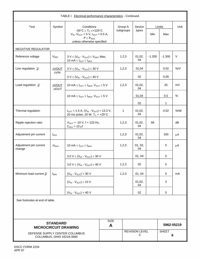
STANDARD MICROCIRCUIT DRAWING
SIZE
A
5962-05219
DEFENSE SUPPLY CENTER COLUMBUS
COLUMBUS, OHIO 43218-3990
REVISION LEVEL C
SHEET 6
DSCC FORM 2234 APR 97
TABLE I. Electrical performance characteristics - Continued.
Limits
Test
Symbol
Conditions
-55°C ≤ TC ≤+125°C VIN -VOUT = 5 V, IOUT = 0.5 A,
P ≤ PMAX unless otherwise specified
Group A subgroups
Device types
Min
Max
Unit
NEGATIVE REGULATOR Reference voltage
VREF
3 V ≤ (VIN - VOUT) ≤ VDIFF Max, 10 mA ≤ IOUT ≤ IMAX
1,2,3
01,02,
04
-1.200
-1.300
V
3 V ≤ (VIN - VOUT) ≤ 30 V
01,04
0.02
Line regulation 1/
ΔVOUT ΔVIN
3 V ≤ (VIN - VOUT) ≤ 40 V
1,2,3
02
0.05
%/V
10 mA ≤ IOUT ≤ IMAX, VOUT ≤ 5 V
01,02,
04
25
mV
01,04
0.5
Load regulation 1/
ΔVOUT ΔIOUT
10 mA ≤ IOUT ≤ IMAX, VOUT ≥ 5 V
1,2,3
02
1
%
Thermal regulation
IOUT = 1.5 A, (VIN - VOUT) = 13.3 V, 20 ms pulse, 20 W, TC = +25°C
1
01,02,
04
0.02
%/W
Ripple rejection ratio
VOUT = -10 V, f = 120 Hz, CADJ = 10 μf
1,2,3
01,02,
04
66
dB
Adjustment pin current
IADJ
1,2,3
01,02,
04
100
μA
10 mA ≤ IOUT ≤ IMAX
01, 02,
04
5
3.0 V ≤ (VIN - VOUT) ≤ 30 V
1,2,3
01, 04
5
Adjustment pin current change
ΔIADJ
3.0 V ≤ (VIN - VOUT) ≤ 40 V
1,2,3
02
5
μA
(VIN - VOUT) = 30 V
01, 04
5
(VIN - VOUT) ≤ 10 V
01,02,
04
3
Minimum load current 2/
IMIN
(VIN - VOUT) = 40 V
1,2,3
02
5
mA
See footnotes at end of table.

STANDARD MICROCIRCUIT DRAWING
SIZE
A
5962-05219
DEFENSE SUPPLY CENTER COLUMBUS
COLUMBUS, OHIO 43218-3990
REVISION LEVEL C
SHEET 7
DSCC FORM 2234 APR 97
TABLE I. Electrical performance characteristics - Continued.
Limits
Test
Symbol
Conditions
-55°C ≤ TC ≤+125°C VIN -VOUT = 5 V, IOUT = 0.5 A,
P ≤ PMAX unless otherwise specified
Group A subgroups
Device types
Min
Max
Unit
NEGATIVE REGULATOR - Continued.
(VIN - VOUT) ≤ 15 V,
1,2,3
01, 04
1.5
(VIN - VOUT) = 30 V, TC = +25°C
1
01, 04
0.24
Current limit
IMAX
(VIN - VOUT) = 40 V, TC = +25°C
1
02
0.24
A
Long term stability 2/
ΔVOUT ΔTIME
TA = +125°C
2
01,02,
04
1
%
Thermal resistance, each regulator, 2/ junction-to-case
θJC
1,2,3
01,02,
04
5
°C/W
1/ Regulation is measured at a constant junction temperature, using pulse testing with a low duty cycle. Changes in output voltage due to heating effects are covered under the specification for thermal regulation. Measurements taken at the output lead must be adjusted for lead resistance. 2/ Parameter shall be tested at intial device characterization and after design or process changes. Parameter shall be guaranteed to the limits specified in table I for all lots not specifically tested.

STANDARD MICROCIRCUIT DRAWING
SIZE
A
5962-05219
DEFENSE SUPPLY CENTER COLUMBUS
COLUMBUS, OHIO 43218-3990
REVISION LEVEL C
SHEET 8
DSCC FORM 2234 APR 97
Table IA. Maximum power dissipation verses case temperature table.
Maximum power dissipation
(Watts)
Case
Temperature (°C)
One regulator "ON"
Both regulators
"ON" 0 30 53 5 29 51
10 28 49 15 27 48 20 26 46 25 25 44 30 24 42 35 23 41 40 22 39 45 21 37 50 20 35 55 19 34 60 18 32 65 17 30 70 16 28 75 15 26 80 14 25 85 13 23 90 12 21 95 11 19 100 10 18 105 9 16 110 8 14 115 7 12 120 6 11 125 5 9 130 4 7 135 3 5 140 2 4 145 1 2 150 0 0
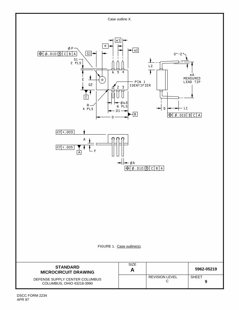
STANDARD MICROCIRCUIT DRAWING
SIZE
A
5962-05219
DEFENSE SUPPLY CENTER COLUMBUS
COLUMBUS, OHIO 43218-3990
REVISION LEVEL C
SHEET 9
DSCC FORM 2234 APR 97
Case outline X.
FIGURE 1. Case outline(s).

STANDARD MICROCIRCUIT DRAWING
SIZE
A
5962-05219
DEFENSE SUPPLY CENTER COLUMBUS
COLUMBUS, OHIO 43218-3990
REVISION LEVEL C
SHEET 10
DSCC FORM 2234 APR 97
Case outline X - Continued.
Inches Millimeters Symbol
Min Max Min Max
A .220 5.59
∅b .028 .032 0.71 0.81
∅b3 .085 .095 2.12 2.41
D .650 .660 16.51 16.76
D1 .410 .420 10.41 10.67
e .100 BSC 2.54 BSC
e1 .200 BSC 5.08 BSC
e2 .108 BSC 2.74 BSC
eA .700 .740 17.78 18.80
E .410 .420 10.41 10.67
F .035 .045 0.90 1.14
G1 .123 BSC 3.12 BSC
G2 .2025 .2125 5.144 5.408
L1 .230 5.84
L2 .150 REF 3.81 REF
∅p .140 .150 3.56 3.81
Q .122 TYP 3.10 TYP
R .065 TYP 1.65 TYP
S1 .028 0.71
NOTES: 1. The U.S. preferred system of measurement is the metric SI. This item was designed using inch-pound units of measurement. In case of problems involving conflicts between the metric and inch-pound units, the inch-pound units shall rule. 2. The package contains a BeO substrate. 3. The case is electrically isolated.
FIGURE 1. Case outline(s) - Continued.

STANDARD MICROCIRCUIT DRAWING
SIZE
A
5962-05219
DEFENSE SUPPLY CENTER COLUMBUS
COLUMBUS, OHIO 43218-3990
REVISION LEVEL C
SHEET 11
DSCC FORM 2234 APR 97
Case outline Y.
FIGURE 1. Case outline(s) - Continued.

STANDARD MICROCIRCUIT DRAWING
SIZE
A
5962-05219
DEFENSE SUPPLY CENTER COLUMBUS
COLUMBUS, OHIO 43218-3990
REVISION LEVEL C
SHEET 12
DSCC FORM 2234 APR 97
Case outline Y - continued.
Inches Millimeters Symbol
Min Max Min Max
A .220 5.59
A2 .015 .025 0.38 0.64
∅b .028 .032 0.71 0.81
∅b3 .085 .095 2.12 2.41
D .650 .660 16.51 16.76
D1 .410 .420 10.41 10.67
e .100 BSC 2.54 BSC
e1 .200 BSC 5.08 BSC
e2 .108 BSC 2.74 BSC
E .410 .420 10.41 10.67
F .035 .045 0.90 1.14
G1 .123 BSC 3.12 BSC
G2 .2025 .2125 5.144 5.408
H .866 .906 22.00 23.01
L1 .055 .065 1.40 1.65
L2 .150 REF 3.81 REF
∅p .140 .150 3.56 3.81
Q .122 TYP 3.10 TYP
R .065 TYP 1.65 TYP
S1 .028 0.71
NOTES: 1. The U.S. preferred system of measurement is the metric SI. This item was designed using inch-pound units of measurement. In case of problems involving conflicts between the metric and inch-pound units, the inch-pound units shall rule. 2. The package contains a BeO substrate. 3. The case is electrically isolated.
FIGURE 1. Case outline(s) - Continued.

STANDARD MICROCIRCUIT DRAWING
SIZE
A
5962-05219
DEFENSE SUPPLY CENTER COLUMBUS
COLUMBUS, OHIO 43218-3990
REVISION LEVEL C
SHEET 13
DSCC FORM 2234 APR 97
Device types 01 and 02 03 04 Case outlines X and Y
Terminal number Terminal symbol
1 2 3 4 5 6
Positive ADJ Positive VOUT Positive VIN
Negative ADJ Negative VIN
Negative VOUT
POS_ADJ_1 POS_VOUT_1 POS_VIN_1 POS_ADJ_2 POS_VIN_2
POS_VOUT_2
NEG_ADJ_1 NEG_VOUT_1 NEG_VIN_1 NEG_ADJ_2 NEG_VIN_2
NEG_VOUT_2
FIGURE 2. Terminal connections.
Device types 01 and 02
FIGURE 3. Block diagram.

STANDARD MICROCIRCUIT DRAWING
SIZE
A
5962-05219
DEFENSE SUPPLY CENTER COLUMBUS
COLUMBUS, OHIO 43218-3990
REVISION LEVEL C
SHEET 14
DSCC FORM 2234 APR 97
Device type 03
Device type 04
FIGURE 3. Block diagram - Continued.

STANDARD MICROCIRCUIT DRAWING
SIZE
A
5962-05219
DEFENSE SUPPLY CENTER COLUMBUS
COLUMBUS, OHIO 43218-3990
REVISION LEVEL C
SHEET 15
DSCC FORM 2234 APR 97
TABLE II. Electrical test requirements.
MIL-PRF-38534 test requirements
Subgroups
(in accordance with MIL-PRF-38534, group A
test table) Interim electrical parameters
Final electrical parameters
1,2,3
Group A test requirements
1,2,3
Group C end-point electrical parameters
1,2,3
End-point electrical parameters for Radiation Hardness Assurance (RHA) devices
Not applicable
* PDA applies to subgroup 1.
4.2 Screening. Screening shall be in accordance with MIL-PRF-38534. The following additional criteria shall apply:
a. Burn-in test, method 1015 of MIL-STD-883.
(1) Test condition A, B, C, or D. The test circuit shall be maintained by the manufacturer under document revision level control and shall be made available to either DSCC-VA or the acquiring activity upon request. Also, the test circuit shall specify the inputs, outputs, biases, and power dissipation, as applicable, in accordance with the intent specified in method 1015 of MIL-STD-883.
(2) TA as specified in accordance with table I of method 1015 of MIL-STD-883.
b. Interim and final electrical test parameters shall be as specified in table II herein, except interim electrical parameter
tests prior to burn-in are optional at the discretion of the manufacturer.
4.3 Conformance and periodic inspections. Conformance inspection (CI) and periodic inspection (PI) shall be in accordance with MIL-PRF-38534 and as specified herein.
4.3.1 Group A inspection (CI). Group A inspection shall be in accordance with MIL-PRF-38534 and as follows:
a. Tests shall be as specified in table II herein.
b. Subgroups 4, 5, 6, 7, 8A, 8B, 9, 10, and 11 shall be omitted.
4.3.2 Group B inspection (PI). Group B inspection shall be in accordance with MIL-PRF-38534.

STANDARD MICROCIRCUIT DRAWING
SIZE
A
5962-05219
DEFENSE SUPPLY CENTER COLUMBUS
COLUMBUS, OHIO 43218-3990
REVISION LEVEL C
SHEET 16
DSCC FORM 2234 APR 97
4.3.3 Group C inspection (PI). Group C inspection shall be in accordance with MIL-PRF-38534 and as follows:
a. End-point electrical parameters shall be as specified in table II herein.
b. Steady-state life test, method 1005 of MIL-STD-883.
(1) Test condition A, B, C, or D. The test circuit shall be maintained by the manufacturer under document revision level control and shall be made available to either DSCC-VA or the acquiring activity upon request. Also, the test circuit shall specify the inputs, outputs, biases, and power dissipation, as applicable, in accordance with the intent specified in method 1005 of MIL-STD-883.
(2) TA as specified in accordance with table I of method 1005 of MIL-STD-883.
(3) Test duration: 1,000 hours, except as permitted by method 1005 of MIL-STD-883.
4.3.4 Group D inspection (PI). Group D inspection shall be in accordance with MIL-PRF-38534.
4.3.5 Radiation Hardness Assurance (RHA) inspection. RHA inspection is not currently applicable to this drawing.
5. PACKAGING
5.1 Packaging requirements. The requirements for packaging shall be in accordance with MIL-PRF-38534.
6. NOTES
6.1 Intended use. Microcircuits conforming to this drawing are intended for use for Government microcircuit applications
(original equipment), design applications, and logistics purposes. 6.2 Replaceability. Microcircuits covered by this drawing will replace the same generic device covered by a contractor-prepared specification or drawing.
6.3 Configuration control of SMD's. All proposed changes to existing SMD's will be coordinated as specified in MIL-PRF-
38534. 6.4 Record of users. Military and industrial users shall inform Defense Supply Center Columbus (DSCC) when a system
application requires configuration control and the applicable SMD. DSCC will maintain a record of users and this list will be used for coordination and distribution of changes to the drawings. Users of drawings covering microelectronic devices (FSC 5962) should contact DSCC-VA, telephone (614) 692-0544.
6.5 Comments. Comments on this drawing should be directed to DSCC-VA, Columbus, Ohio 43218-3990, or telephone (614)
692-1081.
6.6 Sources of supply. Sources of supply are listed in MIL-HDBK-103 and QML-38534. The vendors listed in MIL-HDBK-103 and QML-38534 have submitted a certificate of compliance (see 3.7 herein) to DSCC-VA and have agreed to this drawing.

STANDARD MICROCIRCUIT DRAWING BULLETIN DATE: 08-10-23 Approved sources of supply for SMD 5962-05219 are listed below for immediate acquisition information only and shall be added to MIL-HDBK-103 and QML-38534 during the next revisions. MIL-HDBK-103 and QML-38534 will be revised to include the addition or deletion of sources. The vendors listed below have agreed to this drawing and a certificate of compliance has been submitted to and accepted by DSCC-VA. This information bulletin is superseded by the next dated revisions of MIL-HDBK-103 and QML-38534. DSCC maintains an online database of all current sources of supply at http://www.dscc.dla.mil/Programs/Smcr/.
Standard
microcircuit drawing PIN 1/
Vendor CAGE number
Vendor similar PIN 2/
5962-0521901KXA 5962-0521901KXC 5962-0521901KYA 5962-0521901KYC
88379 88379 88379 88379
VRG8601-201-2S VRG8601-201-1S VRG8602-201-2S VRG8602-201-1S
5962-0521902KXA 5962-0521902KXC 5962-0521902KYA 5962-0521902KYC
3/ 3/ 3/ 3/
VRG8603-201-2S VRG8603-201-1S VRG8604-201-2S VRG8604-201-1S
5962-0521903KXA 5962-0521903KXC 5962-0521903KYA 5962-0521903KYC
88379 88379 88379 88379
VRG8607-201-2S VRG8607-201-1S VRG8608-201-2S VRG8608-201-1S
5962-0521904KXA 5962-0521904KXC 5962-0521904KYA 5962-0521904KYC
88379 88379 88379 88379
VRG8609-201-2S VRG8609-201-1S VRG8610-201-2S VRG8610-201-1S
1/ The lead finish shown for each PIN representing
a hermetic package is the most readily available from the manufacturer listed for that part. If the desired lead finish is not listed contact the Vendor to determine its availability.
2/ Caution. Do not use this number for item acquisition. Items acquired to this number may not satisfy the performance requirements of this drawing.
3/ This device is no longer available.
Vendor CAGE Vendor name number and address
88379 Aeroflex Plainview Incorporated, (Aeroflex Microelectronics Solutions)
35 South Service Road Plainview, NY 11803-4193
The information contained herein is disseminated for convenience only and the Government assumes no liability whatsoever for any inaccuracies in the information bulletin.

REVISIONS
LTR DESCRIPTION DATE (YR-MO-DA) APPROVED
A Table I; changed the max limit for the Dropout voltage test from 1.55 V to 1.30 V. Removed 3/ on the Standard Microcircuit Drawing Bulletin page and added Vendor CAGE number 88379. -sld
09-10-01 Charles F. Saffle
B Added case outline T. -sld 10-06-22 Charles F. Saffle REV
SHEET
REV B B BA B B B B B
SHEET 15 16 17 18 19 20 21 22
REV STATUS REV B B B B B B B B B B B B B B OF SHEETS SHEET 1 2 3 4 5 6 7 8 9 10 11 12 13 14
PMIC N/A
PREPARED BY Steve Duncan
DEFENSE SUPPLY CENTER COLUMBUS COLUMBUS, OHIO 43218-3990
http://www.dscc.dla.mil/
STANDARD MICROCIRCUIT DRAWING
CHECKED BY Greg Cecil
THIS DRAWING IS AVAILABLE
FOR USE BY ALL DEPARTMENTS
AND AGENCIES OF THE DEPARTMENT OF DEFENSE
APPROVED BY Charles F. Saffle
MICROCIRCUIT, HYBRID, DUAL VOLTAGE REGULATOR, POSITIVE AND NEGATIVE, LOW DROPOUT, ADJUSTABLE
DRAWING APPROVAL DATE
09-08-19
AMSC N/A
REVISION LEVEL B
SIZE A
CAGE CODE 67268
5962-09201
SHEET 1 OF
22
DSCC FORM 2233 APR 97 5962-E282-10
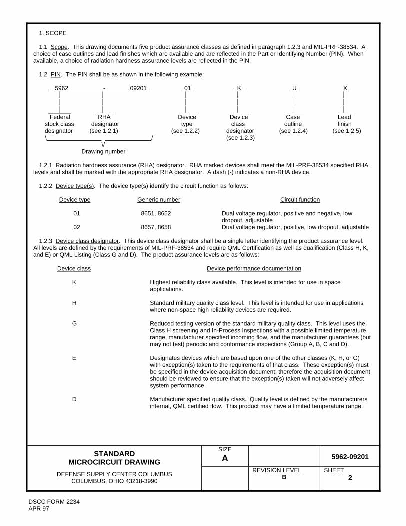
STANDARD MICROCIRCUIT DRAWING
SIZE A
5962-09201
DEFENSE SUPPLY CENTER COLUMBUS
COLUMBUS, OHIO 43218-3990
REVISION LEVEL B
SHEET 2
DSCC FORM 2234 APR 97
1. SCOPE
1.1 Scope. This drawing documents five product assurance classes as defined in paragraph 1.2.3 and MIL-PRF-38534. A choice of case outlines and lead finishes which are available and are reflected in the Part or Identifying Number (PIN). When available, a choice of radiation hardness assurance levels are reflected in the PIN.
1.2 PIN. The PIN shall be as shown in the following example:
5962 - 09201 01 K U X
Federal RHA Device Device Case Lead stock class designator type class outline finish designator (see 1.2.1) (see 1.2.2) designator (see 1.2.4) (see 1.2.5)
\ / (see 1.2.3) \/ Drawing number
1.2.1 Radiation hardness assurance (RHA) designator. RHA marked devices shall meet the MIL-PRF-38534 specified RHA
levels and shall be marked with the appropriate RHA designator. A dash (-) indicates a non-RHA device.
1.2.2 Device type(s). The device type(s) identify the circuit function as follows:
Device type Generic number Circuit function
01 8651, 8652 Dual voltage regulator, positive and negative, low dropout, adjustable 02 8657, 8658 Dual voltage regulator, positive, low dropout, adjustable
1.2.3 Device class designator. This device class designator shall be a single letter identifying the product assurance level. All levels are defined by the requirements of MIL-PRF-38534 and require QML Certification as well as qualification (Class H, K, and E) or QML Listing (Class G and D). The product assurance levels are as follows:
Device class Device performance documentation
K Highest reliability class available. This level is intended for use in space applications. H Standard military quality class level. This level is intended for use in applications
where non-space high reliability devices are required. G Reduced testing version of the standard military quality class. This level uses the
Class H screening and In-Process Inspections with a possible limited temperature range, manufacturer specified incoming flow, and the manufacturer guarantees (but may not test) periodic and conformance inspections (Group A, B, C and D).
E Designates devices which are based upon one of the other classes (K, H, or G)
with exception(s) taken to the requirements of that class. These exception(s) must be specified in the device acquisition document; therefore the acquisition document should be reviewed to ensure that the exception(s) taken will not adversely affect system performance.
D Manufacturer specified quality class. Quality level is defined by the manufacturers internal, QML certified flow. This product may have a limited temperature range.

STANDARD MICROCIRCUIT DRAWING
SIZE A
5962-09201
DEFENSE SUPPLY CENTER COLUMBUS
COLUMBUS, OHIO 43218-3990
REVISION LEVEL B
SHEET 3
DSCC FORM 2234 APR 97
1.2.4 Case outline(s). The case outline(s) are as designated in MIL-STD-1835 and as follows:
Outline letter Descriptive designator Terminals Package style
X See figure 1 6 Thru-Hole Y See figure 1 6 Surface Mount U See figure 1 8 Thru-hole T See figure 1 6 Surface Mount with unformed leads Z See figure 1 8 Surface Mount
1.2.5 Lead finish. The lead finish shall be as specified in MIL-PRF-38534. 1.3 Absolute maximum ratings. 1/
Input voltage: Positive regulator: Device type 01 and 02 ........................................................ 25+VREF Negative regulator: Device type 01 .................................................................... -35 V Input-Output differential voltage: Positive regulator:
Device types 01and 02 ...................................................... 25 V Negative regulator:
Device type 01 .................................................................... 30 V Junction temperature (TJ) .......................................................... +150C Thermal resistance, junction-to-case (JC) each regulator ......... 5C/W Lead temperature (soldering, 10 seconds) ................................ 300C Storage temperature range ........................................................ -65C to +150C
1.4 Recommended operating conditions.
Output voltage range: Postive voltage regulator
Device types 01 and 02 ..................................................... +1.275 V to +23 V dc Negative voltage regulator:
Device type 01 .................................................................... -2.45 V to -25 V dc Case operating temperature range (TC) ...................................... -55C to +125C
2. APPLICABLE DOCUMENTS
2.1 Government specification, standards, and handbooks. The following specification, standards, and handbooks form a part
of this drawing to the extent specified herein. Unless otherwise specified, the issues of these documents are those cited in the solicitation or contract.
DEPARTMENT OF DEFENSE SPECIFICATIONS
MIL-PRF-38534 - Hybrid Microcircuits, General Specification for.
DEPARTMENT OF DEFENSE STANDARDS
MIL-STD-883 - Test Method Standard Microcircuits. MIL-STD-1835 - Interface Standard Electronic Component Case Outlines.
DEPARTMENT OF DEFENSE HANDBOOKS
MIL-HDBK-103 - List of Standard Microcircuit Drawings. MIL-HDBK-780 - Standard Microcircuit Drawings.
________ 1/ Stresses above the absolute maximum ratings may cause permanent damage to the device. Extended operation at the maximum levels may degrade performance and affect reliability.

STANDARD MICROCIRCUIT DRAWING
SIZE A
5962-09201
DEFENSE SUPPLY CENTER COLUMBUS
COLUMBUS, OHIO 43218-3990
REVISION LEVEL B
SHEET 4
DSCC FORM 2234 APR 97
(Copies of these documents are available online at https://assist.daps.dla.mil/quicksearch/ or from the Standardization Document Order Desk, 700 Robbins Avenue, Building 4D, Philadelphia, PA 19111-5094.)
2.2 Order of precedence. In the event of a conflict between the text of this drawing and the references cited herein, the text of this drawing takes precedence. Nothing in this document, however, supersedes applicable laws and regulations unless a specific exemption has been obtained.
3. REQUIREMENTS
3.1 Item requirements. The individual item performance requirements for device classes D, E, G, H, and K shall be in accordance with MIL-PRF-38534. Compliance with MIL-PRF-38534 shall include the performance of all tests herein or as designated in the device manufacturer's Quality Management (QM) plan or as designated for the applicable device class. The manufacturer may eliminate, modify or optimize the tests and inspections herein, however the performance requirements as defined in MIL-PRF-38534 shall be met for the applicable device class. In addition, the modification in the QM plan shall not affect the form, fit, or function of the device for the applicable device class.
3.2 Design, construction, and physical dimensions. The design, construction, and physical dimensions shall be as specified in MIL-PRF-38534 and herein.
3.2.1 Case outline(s). The case outline(s) shall be in accordance with 1.2.4 herein and figure 1.
3.2.2 Terminal connections. The terminal connections shall be as specified on figure 2. 3.2.3 Block diagram. The block diagram shall be as specified on figure 3.
3.2.4 Maximum power dissipation verses case temperature table. The maximum power dissipation verses case temperature
is specified in table IA.
3.3 Electrical performance characteristics. Unless otherwise specified herein, the electrical performance characteristics are as specified in table I and shall apply over the full specified operating temperature range.
3.4 Electrical test requirements. The electrical test requirements shall be the subgroups specified in table II. The electrical tests for each subgroup are defined in table I.
3.5 Marking of device(s). Marking of device(s) shall be in accordance with MIL-PRF-38534. The device shall be marked with the PIN listed in 1.2 herein. In addition, the manufacturer's vendor similar PIN may also be marked.
3.6 Data. In addition to the general performance requirements of MIL-PRF-38534, the manufacturer of the device described herein shall maintain the electrical test data (variables format) from the initial quality conformance inspection group A lot sample, for each device type listed herein. Also, the data should include a summary of all parameters manually tested, and for those which, if any, are guaranteed. This data shall be maintained under document revision level control by the manufacturer and be made available to the preparing activity (DSCC-VA) upon request.
3.7 Certificate of compliance. A certificate of compliance shall be required from a manufacturer in order to supply to this drawing. The certificate of compliance (original copy) submitted to DSCC-VA shall affirm that the manufacturer's product meets the performance requirements of MIL-PRF-38534 and herein.
3.8 Certificate of conformance. A certificate of conformance as required in MIL-PRF-38534 shall be provided with each lot of microcircuits delivered to this drawing.
4. VERIFICATION
4.1 Sampling and inspection. Sampling and inspection procedures shall be in accordance with MIL-PRF-38534 or as modified in the device manufacturer's Quality Management (QM) plan. The modification in the QM plan shall not affect the form, fit, or function as described herein.

STANDARD MICROCIRCUIT DRAWING
SIZE A
5962-09201
DEFENSE SUPPLY CENTER COLUMBUS
COLUMBUS, OHIO 43218-3990
REVISION LEVEL B
SHEET 5
DSCC FORM 2234 APR 97
TABLE I. Electrical performance characteristics.
Test
Symbol
Conditions
-55C TC +125C P PMAX
unless otherwise specified
Group A subgroups
Device types
Limits
Unit
Min
Max
POSITIVE REGULATOR Reference voltage
VREF
1.5 V (VIN - VOUT) 15 V, ILOAD = 10 mA
1,2,3
01,02
1.210
1.275
V
Line regulation 1/
ΔVOUT
ΔVIN
1.5 V (VIN - VOUT) 15 V, ILOAD = 10 mA
1,2,3
01,02
0.25
%
Load regulation 1/
ΔVOUT
ΔIOUT
10 mA IOUT 1.0 A, (VIN - VOUT) = 3 V
1,2,3
01,02
0.3
%
Thermal regulation
30 ms pulse, TC = +25C
1
01,02
0.04
%/W
Dropout voltage
VDROP
VREF = 1%, IOUT = 1.0 A
1,2,3
01,02
1.30
V
Ripple rejection
IOUT = 1.0 A, (VIN - VOUT) = 3 V, f = 120 Hz, CADJ = COUT = 25 F
1,2,3
01,02
60
dB
Adjustment pin current
IADJ
TC = +25C
1
01,02
120
A
Adjustment pin current change
IADJ
10 mA IOUT 1.0 A, 1.5 V (VIN - VOUT) 15 V
1,2,3
01,02
5
A
Minimum load current 2/
IMIN
(VIN - VOUT) = 25 V
1,2,3
01,02
10
mA
Current limit
IMAX
(VIN - VOUT) 5 V
1,2,3
01,02
1.0
A
(VIN - VOUT) 25 V
1,2,3
0.047
VREF Long term stability 2/
ΔVOUT
ΔTIME
Burn-in: TC = +125C at 1000 hours minimum, tested at +25C
1
01,02
0.3
%
NEGATIVE REGULATOR Reference voltage
VREF
VIN - VOUT = -1.2 V to -28 V, 1 mA IOUT 3 A, VOUT = -5 V, TC = +25C and -55C
1,3
01
-2.29
-2.45
V
See footnotes at end of table.

STANDARD MICROCIRCUIT DRAWING
SIZE A
5962-09201
DEFENSE SUPPLY CENTER COLUMBUS
COLUMBUS, OHIO 43218-3990
REVISION LEVEL B
SHEET 6
DSCC FORM 2234 APR 97
TABLE I. Electrical performance characteristics - Continued.
Test
Symbol
Conditions
-55C TC +125C P PMAX
unless otherwise specified
Group A subgroups
Device types
Limits
Unit
Min
Max
NEGATIVE REGULATOR - CONTINUED Dropout Voltage
VDROP
IOUT = 0.5 A, VOUT = -5 V
1,2,3
01
V
IOUT = 3 A, VOUT = -5 V
1.05
Ripple rejection
IOUT = 1.0 A, (VIN - VOUT) = 3 V, f = 120 Hz, CADJ = COUT = 25 F
1,2,3
01
60
dB
Line regulation 1/
ΔVOUT
ΔVIN
1 V VIN - VOUT) 20V, VOUT = -5 V
1,2,3
01
0.02
%/V
Load regulation 1/
ΔVOUT
ΔIOUT
5 mA IOUT 3 A, (VIN - VOUT) = -15 V to -10 V, VOUT = -5 V
1,2,3
01
0.8
%
Thermal regulation 2/
VIN - VOUT = 10 V, IOUT = 5 mA to 2 A, TC = +25C
1
01
0.014
%/W
Minimum input voltage
VIN MIN
IOUT = 3 A, VOUT = VREF
1,2,3
01
V
Internal Current limit
IMAX
-1.5 V (VIN - VOUT) -10 V, TC = +25C and -55C
1,3
01
3.3
4.55
A
(VIN - VOUT) =-15 V, TC = +25C and -55C
2.0
4.5
(VIN - VOUT) -20 V, TC = +25C and -55C
1.0
3.1
(VIN - VOUT) = -30 V, 2/ TC = +25C and -55C
0.2
1.6
External current limit
ILIM
RLIM = 5 k
1,2,3
01
2.7
3. 7
A
RLIM = 15 k
0.9
1.6
See footnotes at end of table.

STANDARD MICROCIRCUIT DRAWING
SIZE A
5962-09201
DEFENSE SUPPLY CENTER COLUMBUS
COLUMBUS, OHIO 43218-3990
REVISION LEVEL B
SHEET 7
DSCC FORM 2234 APR 97
TABLE I. Electrical performance characteristics - Continued.
Test
Symbol
Conditions
-55°C TC +125C P PMAX
unless otherwise specified
Group A subgroups
Device types
Limits
Unit
Min
Max
NEGATIVE REGULATOR - CONTINUED Quiescent supply current
IQ
IOUT = 5 mA, VOUT = VREF, (-4 V VIN -25 V)
1,2,3
01
3.5
mA
Supply current change with load
IQ
(VIN - VOUT) = .25 V +(.25 x IOUT)
1,2,3
01
35
mA/A
(VIN - VOUT) -2 V
21
1/ Regulation is measured at a constant junction temperature, using pulse testing with a low duty cycle. Changes in output voltage due to heating effects are covered under the specification for thermal regulation. Measurements taken at the output lead must be adjusted for lead resistance. 2/ Parameter shall be tested at intial device characterization and after design or process changes. Parameter shall be guaranteed to the limits specified in table I for all lots not specifically tested.

STANDARD MICROCIRCUIT DRAWING
SIZE A
5962-09201
DEFENSE SUPPLY CENTER COLUMBUS
COLUMBUS, OHIO 43218-3990
REVISION LEVEL B
SHEET 8
DSCC FORM 2234 APR 97
Table IA. Maximum power dissipation verses case temperature table.
Case
Temperature (C)
Maximum power dissipation
(Watts)
One regulator "ON"
Both regulators
"ON" 0 30 53 5 29 51
10 28 49 15 27 48 20 26 46 25 25 44 30 24 42 35 23 41 40 22 39 45 21 37 50 20 35 55 19 34 60 18 32 65 17 30 70 16 28 75 15 26 80 14 25 85 13 23 90 12 21 95 11 19
100 10 18 105 9 16 110 8 14 115 7 12 120 6 11 125 5 9 130 4 7 135 3 5 140 2 4 145 1 2 150 0 0

STANDARD MICROCIRCUIT DRAWING
SIZE A
5962-09201
DEFENSE SUPPLY CENTER COLUMBUS
COLUMBUS, OHIO 43218-3990
REVISION LEVEL B
SHEET 9
DSCC FORM 2234 APR 97
Case U
FIGURE 1. Case outline(s).

STANDARD MICROCIRCUIT DRAWING
SIZE A
5962-09201
DEFENSE SUPPLY CENTER COLUMBUS
COLUMBUS, OHIO 43218-3990
REVISION LEVEL B
SHEET 10
DSCC FORM 2234 APR 97
Case U - Continued.
Symbol Inches Millimeters
Min Max Min Max
A .220 5.59
b .028 .032 0.71 0.81
b3 .085 .095 2.12 2.41
D .750 .760 19.05 19.30
D1 .510 .520 12.95 13.21
e .100 BSC 2.54 BSC
e1 .300 BSC 7.62 BSC
e2 .108 BSC 2.74 BSC
eA .700 .740 17.78 18.80
E .410 .420 10.41 10.67
F .035 .045 0.90 1.14
G1 .632 BSC 16.05 BSC
G2 .2025 .2125 5.144 5.408
L1 .230 5.84
L2 .150 REF 3.81 REF
p .140 .150 3.56 3.81
Q .122 TYP 3.10 TYP
R .065 TYP 1.65 TYP
S1 .028 0.71
NOTES: 1. The U.S. preferred system of measurement is the metric SI. This item was designed using inch-pound units of measurement. In case of problems involving conflicts between the metric and inch-pound units, the inch-pound units shall rule. 2. The package contains a BeO substrate. 3. The case is electrically isolated.
FIGURE 1. Case outline(s) - Continued.
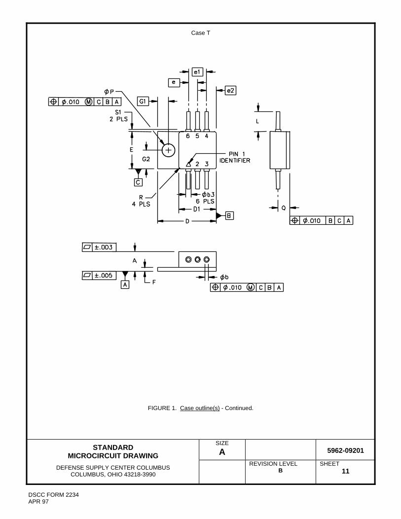
STANDARD MICROCIRCUIT DRAWING
SIZE A
5962-09201
DEFENSE SUPPLY CENTER COLUMBUS
COLUMBUS, OHIO 43218-3990
REVISION LEVEL B
SHEET 11
DSCC FORM 2234 APR 97
Case T
FIGURE 1. Case outline(s) - Continued.
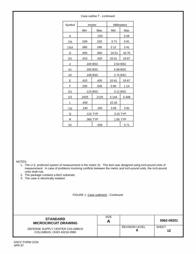
STANDARD MICROCIRCUIT DRAWING
SIZE A
5962-09201
DEFENSE SUPPLY CENTER COLUMBUS
COLUMBUS, OHIO 43218-3990
REVISION LEVEL B
SHEET 12
DSCC FORM 2234 APR 97
Case outline T - continued.
Symbol Inches Millimeters
Min Max Min Max
A .220 5.59
b .028 .032 0.71 0.81
b3 .085 .095 2.12 2.41
D .650 .660 16.51 16.76
D1 .410 .420 10.41 10.67
e .100 BSC 2.54 BSC
e1 .200 BSC 5.08 BSC
e2 .108 BSC 2.74 BSC
E .410 .420 10.41 10.67
F .035 .045 0.90 1.14
G1 .123 BSC 3.12 BSC
G2 .2025 .2125 5.144 5.408
L .400 10.16
p .140 .150 3.56 3.81
Q .122 TYP 3.10 TYP
R .065 TYP 1.65 TYP
S1 .028 0.71
NOTES: 1. The U.S. preferred system of measurement is the metric SI. This item was designed using inch-pound units of measurement. In case of problems involving conflicts between the metric and inch-pound units, the inch-pound units shall rule. 2. The package contains a BeO substrate. 3. The case is electrically isolated.
FIGURE 1. Case outline(s) - Continued.

STANDARD MICROCIRCUIT DRAWING
SIZE A
5962-09201
DEFENSE SUPPLY CENTER COLUMBUS
COLUMBUS, OHIO 43218-3990
REVISION LEVEL B
SHEET 13
DSCC FORM 2234 APR 97
Case outline X.
FIGURE 1. Case outline(s) - Continued.

STANDARD MICROCIRCUIT DRAWING
SIZE A
5962-09201
DEFENSE SUPPLY CENTER COLUMBUS
COLUMBUS, OHIO 43218-3990
REVISION LEVEL B
SHEET 14
DSCC FORM 2234 APR 97
Case outline X - Continued.
Symbol Inches Millimeters
Min Max Min Max
A .220 5.59
b .028 .032 0.71 0.81
b3 .085 .095 2.12 2.41
D .650 .660 16.51 16.76
D1 .410 .420 10.41 10.67
e .100 BSC 2.54 BSC
e1 .200 BSC 5.08 BSC
e2 .108 BSC 2.74 BSC
eA .700 .740 17.78 18.80
E .410 .420 10.41 10.67
F .035 .045 0.90 1.14
G1 .123 BSC 3.12 BSC
G2 .2025 .2125 5.144 5.408
L1 .230 5.84
L2 .150 REF 3.81 REF
p .140 .150 3.56 3.81
Q .122 TYP 3.10 TYP
R .065 TYP 1.65 TYP
S1 .028 0.71
NOTES: 1. The U.S. preferred system of measurement is the metric SI. This item was designed using inch-pound units of measurement. In case of problems involving conflicts between the metric and inch-pound units, the inch-pound units shall rule. 2. The package contains a BeO substrate. 3. The case is electrically isolated.
FIGURE 1. Case outline(s) - Continued.

STANDARD MICROCIRCUIT DRAWING
SIZE A
5962-09201
DEFENSE SUPPLY CENTER COLUMBUS
COLUMBUS, OHIO 43218-3990
REVISION LEVEL B
SHEET 15
DSCC FORM 2234 APR 97
Case outline Y.
FIGURE 1. Case outline(s) - Continued.

STANDARD MICROCIRCUIT DRAWING
SIZE A
5962-09201
DEFENSE SUPPLY CENTER COLUMBUS
COLUMBUS, OHIO 43218-3990
REVISION LEVEL B
SHEET 16
DSCC FORM 2234 APR 97
Case outline Y - continued.
Symbol Inches Millimeters
Min Max Min Max
A .220 5.59
A2 .015 .025 0.38 0.64
b .028 .032 0.71 0.81
b3 .085 .095 2.12 2.41
D .650 .660 16.51 16.76
D1 .410 .420 10.41 10.67
e .100 BSC 2.54 BSC
e1 .200 BSC 5.08 BSC
e2 .108 BSC 2.74 BSC
E .410 .420 10.41 10.67
F .035 .045 0.90 1.14
G1 .123 BSC 3.12 BSC
G2 .2025 .2125 5.144 5.408
H .866 .906 22.00 23.01
L1 .055 .065 1.40 1.65
L2 .150 REF 3.81 REF
p .140 .150 3.56 3.81
Q .122 TYP 3.10 TYP
R .065 TYP 1.65 TYP
S1 .028 0.71
NOTES: 1. The U.S. preferred system of measurement is the metric SI. This item was designed using inch-pound units of measurement. In case of problems involving conflicts between the metric and inch-pound units, the inch-pound units shall rule. 2. The package contains a BeO substrate. 3. The case is electrically isolated.
FIGURE 1. Case outline(s) - Continued.

STANDARD MICROCIRCUIT DRAWING
SIZE A
5962-09201
DEFENSE SUPPLY CENTER COLUMBUS
COLUMBUS, OHIO 43218-3990
REVISION LEVEL B
SHEET 17
DSCC FORM 2234 APR 97
Case Z
FIGURE 1. Case outlines(s) - Continued.

STANDARD MICROCIRCUIT DRAWING
SIZE A
5962-09201
DEFENSE SUPPLY CENTER COLUMBUS
COLUMBUS, OHIO 43218-3990
REVISION LEVEL B
SHEET 18
DSCC FORM 2234 APR 97
Case Z - Continued.
Symbol Inches Millimeters
Min Max Min Max
A .220 5.59
A1 .015 .025 0.38 0.64
b .028 .032 0.71 0.81
b3 .085 .095 2.12 2.41
D .750 .760 19.05 19.30
D1 .510 .520 12.95 13.21
e .100 BSC 2.54 BSC
e1 .300 BSC 7.62 BSC
e2 .108 BSC 2.74 BSC
E .410 .420 10.41 10.67
F .035 .045 0.90 1.14
G1 .632 BSC 16.05 BSC
G2 .2025 .2125 5.144 5.408
H .866 .906 22.00 23.01
L1 .055 .065 1.40 1.65
L2 .150 REF 3.81 REF
p .140 .150 3.56 3.81
Q .122 TYP 3.10 TYP
R .065 TYP 1.65 TYP
S1 .028 0.71
NOTES: 1. The U.S. preferred system of measurement is the metric SI. This item was designed using inch-pound units of measurement. In case of problems involving conflicts between the metric and inch-pound units, the inch-pound units shall rule. 2. The package contains a BeO substrate. 3. The case is electrically isolated.
FIGURE 1. Case outline(s) - Continued.

STANDARD MICROCIRCUIT DRAWING
SIZE A
5962-09201
DEFENSE SUPPLY CENTER COLUMBUS
COLUMBUS, OHIO 43218-3990
REVISION LEVEL B
SHEET 19
DSCC FORM 2234 APR 97
Device types 01 02 Case outlines U and Z X , Y and T
Terminal number Terminal symbol
1 2 3 4 5 6 7 8
POS_ ADJ_1 NEG_REF_2 NEG_VOUT_2 NEG_VIN_2
NEG_GND_2 NEG_FB_2
POS_VOUT_1 POS_VIN_1
POS_ADJ_1 POS_VOUT_1 POS_VIN_1 POS_ADJ_2 POS_VIN_2
POS_VOUT_2
FIGURE 2. Terminal connections.
Device type 01
FIGURE 3. Block diagram.

STANDARD MICROCIRCUIT DRAWING
SIZE A
5962-09201
DEFENSE SUPPLY CENTER COLUMBUS
COLUMBUS, OHIO 43218-3990
REVISION LEVEL B
SHEET 20
DSCC FORM 2234 APR 97
Device type 02
FIGURE 3. Block diagram - Continued.

STANDARD MICROCIRCUIT DRAWING
SIZE A
5962-09201
DEFENSE SUPPLY CENTER COLUMBUS
COLUMBUS, OHIO 43218-3990
REVISION LEVEL B
SHEET 21
DSCC FORM 2234 APR 97
TABLE II. Electrical test requirements.
MIL-PRF-38534 test requirements Subgroups
(in accordance with MIL-PRF-38534, group A
test table) Interim electrical parameters
---
Final electrical parameters
1,2,3
Group A test requirements
1,2,3
Group C end-point electrical parameters
1,2,3
End-point electrical parameters for Radiation Hardness Assurance (RHA) devices
Not applicable
* PDA applies to subgroup 1.
4.2 Screening. Screening shall be in accordance with MIL-PRF-38534. The following additional criteria shall apply:
a. Burn-in test, method 1015 of MIL-STD-883.
(1) Test condition A, B, C, or D. The test circuit shall be maintained by the manufacturer under document revision level control and shall be made available to either DSCC-VA or the acquiring activity upon request. Also, the test circuit shall specify the inputs, outputs, biases, and power dissipation, as applicable, in accordance with the intent specified in method 1015 of MIL-STD-883.
(2) TA as specified in accordance with table I of method 1015 of MIL-STD-883.
b. Interim and final electrical test parameters shall be as specified in table II herein, except interim electrical parameter
tests prior to burn-in are optional at the discretion of the manufacturer.
4.3 Conformance and periodic inspections. Conformance inspection (CI) and periodic inspection (PI) shall be in accordance with MIL-PRF-38534 and as specified herein.
4.3.1 Group A inspection (CI). Group A inspection shall be in accordance with MIL-PRF-38534 and as follows:
a. Tests shall be as specified in table II herein.
b. Subgroups 4, 5, 6, 7, 8A, 8B, 9, 10, and 11 shall be omitted.
4.3.2 Group B inspection (PI). Group B inspection shall be in accordance with MIL-PRF-38534.
STANDARD MICROCIRCUIT DRAWING
SIZE A
5962-09201
DEFENSE SUPPLY CENTER COLUMBUS
COLUMBUS, OHIO 43218-3990
REVISION LEVEL B
SHEET 22
DSCC FORM 2234 APR 97
4.3.3 Group C inspection (PI). Group C inspection shall be in accordance with MIL-PRF-38534 and as follows:
a. End-point electrical parameters shall be as specified in table II herein.
b. Steady-state life test, method 1005 of MIL-STD-883.
(1) Test condition A, B, C, or D. The test circuit shall be maintained by the manufacturer under document revision level control and shall be made available to either DSCC-VA or the acquiring activity upon request. Also, the test circuit shall specify the inputs, outputs, biases, and power dissipation, as applicable, in accordance with the intent specified in method 1005 of MIL-STD-883.
(2) TA as specified in accordance with table I of method 1005 of MIL-STD-883.
(3) Test duration: 1,000 hours, except as permitted by method 1005 of MIL-STD-883.
4.3.4 Group D inspection (PI). Group D inspection shall be in accordance with MIL-PRF-38534.
4.3.5 Radiation Hardness Assurance (RHA) inspection. RHA inspection is not currently applicable to this drawing.
5. PACKAGING
5.1 Packaging requirements. The requirements for packaging shall be in accordance with MIL-PRF-38534.
6. NOTES
6.1 Intended use. Microcircuits conforming to this drawing are intended for use for Government microcircuit applications
(original equipment), design applications, and logistics purposes. 6.2 Replaceability. Microcircuits covered by this drawing will replace the same generic device covered by a contractor-prepared specification or drawing.
6.3 Configuration control of SMD's. All proposed changes to existing SMD's will be coordinated as specified in MIL-PRF-
38534. 6.4 Record of users. Military and industrial users shall inform Defense Supply Center Columbus (DSCC) when a system
application requires configuration control and the applicable SMD. DSCC will maintain a record of users and this list will be used for coordination and distribution of changes to the drawings. Users of drawings covering microelectronic devices (FSC 5962) should contact DSCC-VA, telephone (614) 692-0544.
6.5 Comments. Comments on this drawing should be directed to DSCC-VA, Columbus, Ohio 43218-3990, or telephone (614)
692-1081.
6.6 Sources of supply. Sources of supply are listed in MIL-HDBK-103 and QML-38534. The vendors listed in MIL-HDBK-103 and QML-38534 have submitted a certificate of compliance (see 3.7 herein) to DSCC-VA and have agreed to this drawing.

STANDARD MICROCIRCUIT DRAWING BULLETIN DATE: 10-06-22 Approved sources of supply for SMD 5962-09201 are listed below for immediate acquisition information only and shall be added to MIL-HDBK-103 and QML-38534 during the next revisions. MIL-HDBK-103 and QML-38534 will be revised to include the addition or deletion of sources. The vendors listed below have agreed to this drawing and a certificate of compliance has been submitted to and accepted by DSCC-VA. This information bulletin is superseded by the next dated revisions of MIL-HDBK-103 and QML-38534. DSCC maintains an online database of all current sources of supply at http://www.dscc.dla.mil/Programs/Smcr/.
Standard
microcircuit drawing PIN 1/
Vendor CAGE
number
Vendor similar PIN 2/
5962-0920101KUA 5962-0920101KUC 5962-0920101KZA 5962-0920101KZC
88379 88379 88379 88379
VRG8651-201-2S VRG8651-201-1S VRG8652-201-2S VRG8652-201-1S
5962-0920102KXA 5962-0920102KXC 5962-0920102KYA 5962-0920102KYC 5962-0920102KTC
88379 88379 88379 88379 88379
VRG8657-201-2S VRG8657-201-1S VRG8658-201-2S VRG8658-201-1S VRG8658-202-1S
1/ The lead finish shown for each PIN representing
a hermetic package is the most readily available from the manufacturer listed for that part. If the desired lead finish is not listed contact the Vendor to determine its availability.
2/ Caution. Do not use this number for item acquisition. Items acquired to this number may not satisfy the performance requirements of this drawing.
Vendor CAGE Vendor name number and address
88379 Aeroflex Plainview Incorporated, (Aeroflex Microelectronics Solutions)
35 South Service Road Plainview, NY 11803-4193
The information contained herein is disseminated for convenience only and the Government assumes no liability whatsoever for any inaccuracies in the information bulletin.

REVISIONS
LTR DESCRIPTION DATE (YR-MO-DA) APPROVED
REV
SHEET
REV
SHEET
REV STATUS REV OF SHEETS SHEET 1 2 3 4 5 6 7 8 9 10 11 12 13
PMIC N/A PREPARED BY Steve Duncan
DEFENSE SUPPLY CENTER COLUMBUS COLUMBUS, OHIO 43218-3990
http://www.dscc.dla.mil/ STANDARD MICROCIRCUIT
DRAWING
CHECKED BY Greg Cecil
THIS DRAWING IS AVAILABLE
FOR USE BY ALL DEPARTMENTS
AND AGENCIES OF THE DEPARTMENT OF DEFENSE
APPROVED BY Charles F. Saffle
MICROCIRCUIT, HYBRID, VOLTAGE REGULATOR, POSTIVE AND NEGATIVE, ADJUSTABLE DRAWING APPROVAL DATE
09-12-08
AMSC N/A
REVISION LEVEL
SIZE A
CAGE CODE 67268
5962-09206
SHEET 1 OF
13
DSCC FORM 2233 APR 97 5962-E049-09

STANDARD MICROCIRCUIT DRAWING
SIZE A
5962-09206
DEFENSE SUPPLY CENTER COLUMBUS
COLUMBUS, OHIO 43218-3990
REVISION LEVEL
SHEET 2
DSCC FORM 2234 APR 97
1. SCOPE
1.1 Scope. This drawing documents five product assurance classes as defined in paragraph 1.2.3 and MIL-PRF-38534. A choice of case outlines and lead finishes which are available and are reflected in the Part or Identifying Number (PIN). When available, a choice of radiation hardness assurance levels are reflected in the PIN.
1.2 PIN. The PIN shall be as shown in the following example:
5962 - 09206 01 K X X
Federal RHA Device Device Case Lead stock class designator type class outline finish designator (see 1.2.1) (see 1.2.2) designator (see 1.2.4) (see 1.2.5)
\ / (see 1.2.3) \/ Drawing number
1.2.1 Radiation hardness assurance (RHA) designator. RHA marked devices shall meet the MIL-PRF-38534 specified RHA
levels and shall be marked with the appropriate RHA designator. A dash (-) indicates a non-RHA device.
1.2.2 Device type(s). The device type(s) identify the circuit function as follows:
Device type Generic number Circuit function
01 8660 Voltage regulator, positive, adjustable 02 8661 Voltage regulator, negative, adjustable
1.2.3 Device class designator. This device class designator shall be a single letter identifying the product assurance level. All levels are defined by the requirements of MIL-PRF-38534 and require QML Certification as well as qualification (Class H, K, and E) or QML Listing (Class G and D). The product assurance levels are as follows:
Device class Device performance documentation
K Highest reliability class available. This level is intended for use in space applications. H Standard military quality class level. This level is intended for use in applications
where non-space high reliability devices are required. G Reduced testing version of the standard military quality class. This level uses the
Class H screening and In-Process Inspections with a possible limited temperature range, manufacturer specified incoming flow, and the manufacturer guarantees (but may not test) periodic and conformance inspections (Group A, B, C and D).
E Designates devices which are based upon one of the other classes (K, H, or G)
with exception(s) taken to the requirements of that class. These exception(s) must be specified in the device acquisition document; therefore the acquisition document should be reviewed to ensure that the exception(s) taken will not adversely affect system performance.
D Manufacturer specified quality class. Quality level is defined by the manufacturers internal, QML certified flow. This product may have a limited temperature range.

STANDARD MICROCIRCUIT DRAWING
SIZE A
5962-09206
DEFENSE SUPPLY CENTER COLUMBUS
COLUMBUS, OHIO 43218-3990
REVISION LEVEL
SHEET 3
DSCC FORM 2234 APR 97
1.2.4 Case outline(s). The case outline(s) are as designated in MIL-STD-1835 and as follows:
Outline letter Descriptive designator Terminals Package style
X See figure 1 3 Bottom terminal chip carrier, ceramic
1.2.5 Lead finish. The lead finish shall be as specified in MIL-PRF-38534. 1.3 Absolute maximum ratings. 1/
Input-Output differential voltage: Positive regulator
Device type 01 .................................................................... 40 V Negative regulator:
Device type 02 .................................................................... -30 V Operating junction temperature range ....................................... -55°C to +150°C Junction temperature (TJ) .......................................................... +150°C Thermal resistance, junction-to-case (θJC) each regulator ......... 3°C/W Lead temperature (soldering, 10 seconds) ................................ 300°C Storage temperature range ........................................................ -65°C to +150°C
1.4 Recommended operating conditions.
Output voltage range: Postive voltage regulator
Device type 01 .................................................................... +1.25 V to +37 V dc Negative voltage regulator:
Device type 02 .................................................................... -1.25 V to -27 V dc Case operating temperature range (TC) ...................................... -55°C to +125°C
2. APPLICABLE DOCUMENTS
2.1 Government specification, standards, and handbooks. The following specification, standards, and handbooks form a part
of this drawing to the extent specified herein. Unless otherwise specified, the issues of these documents are those cited in the solicitation or contract.
DEPARTMENT OF DEFENSE SPECIFICATIONS
MIL-PRF-38534 - Hybrid Microcircuits, General Specification for.
DEPARTMENT OF DEFENSE STANDARDS
MIL-STD-883 - Test Method Standard Microcircuits. MIL-STD-1835 - Interface Standard Electronic Component Case Outlines.
DEPARTMENT OF DEFENSE HANDBOOKS
MIL-HDBK-103 - List of Standard Microcircuit Drawings. MIL-HDBK-780 - Standard Microcircuit Drawings.
(Copies of these documents are available online at https://assist.daps.dla.mil/quicksearch/ or from the Standardization
Document Order Desk, 700 Robbins Avenue, Building 4D, Philadelphia, PA 19111-5094.)
________ 1/ Stresses above the absolute maximum ratings may cause permanent damage to the device. Extended operation at the maximum levels may degrade performance and affect reliability.

STANDARD MICROCIRCUIT DRAWING
SIZE A
5962-09206
DEFENSE SUPPLY CENTER COLUMBUS
COLUMBUS, OHIO 43218-3990
REVISION LEVEL
SHEET 4
DSCC FORM 2234 APR 97
2.2 Order of precedence. In the event of a conflict between the text of this drawing and the references cited herein, the text of this drawing takes precedence. Nothing in this document, however, supersedes applicable laws and regulations unless a specific exemption has been obtained.
3. REQUIREMENTS
3.1 Item requirements. The individual item performance requirements for device classes D, E, G, H, and K shall be in accordance with MIL-PRF-38534. Compliance with MIL-PRF-38534 shall include the performance of all tests herein or as designated in the device manufacturer's Quality Management (QM) plan or as designated for the applicable device class. The manufacturer may eliminate, modify or optimize the tests and inspections herein, however the performance requirements as defined in MIL-PRF-38534 shall be met for the applicable device class. In addition, the modification in the QM plan shall not affect the form, fit, or function of the device for the applicable device class.
3.2 Design, construction, and physical dimensions. The design, construction, and physical dimensions shall be as specified in MIL-PRF-38534 and herein.
3.2.1 Case outline(s). The case outline(s) shall be in accordance with 1.2.4 herein and figure 1.
3.2.2 Terminal connections. The terminal connections shall be as specified on figure 2. 3.2.3 Block diagram. The block diagram shall be as specified on figure 3.
3.2.4 Maximum power dissipation verses case temperature chart. The maximum power dissipation verses case temperature
is specified on figure 4.
3.3 Electrical performance characteristics. Unless otherwise specified herein, the electrical performance characteristics are as specified in table I and shall apply over the full specified operating temperature range.
3.4 Electrical test requirements. The electrical test requirements shall be the subgroups specified in table II. The electrical tests for each subgroup are defined in table I.
3.5 Marking of device(s). Marking of device(s) shall be in accordance with MIL-PRF-38534. The device shall be marked with the PIN listed in 1.2 herein. In addition, the manufacturer's vendor similar PIN may also be marked.
3.6 Data. In addition to the general performance requirements of MIL-PRF-38534, the manufacturer of the device described herein shall maintain the electrical test data (variables format) from the initial quality conformance inspection group A lot sample, for each device type listed herein. Also, the data should include a summary of all parameters manually tested, and for those which, if any, are guaranteed. This data shall be maintained under document revision level control by the manufacturer and be made available to the preparing activity (DSCC-VA) upon request.
3.7 Certificate of compliance. A certificate of compliance shall be required from a manufacturer in order to supply to this drawing. The certificate of compliance (original copy) submitted to DSCC-VA shall affirm that the manufacturer's product meets the performance requirements of MIL-PRF-38534 and herein.
3.8 Certificate of conformance. A certificate of conformance as required in MIL-PRF-38534 shall be provided with each lot of microcircuits delivered to this drawing.
4. VERIFICATION
4.1 Sampling and inspection. Sampling and inspection procedures shall be in accordance with MIL-PRF-38534 or as modified in the device manufacturer's Quality Management (QM) plan. The modification in the QM plan shall not affect the form, fit, or function as described herein.

STANDARD MICROCIRCUIT DRAWING
SIZE A
5962-09206
DEFENSE SUPPLY CENTER COLUMBUS
COLUMBUS, OHIO 43218-3990
REVISION LEVEL
SHEET 5
DSCC FORM 2234 APR 97
TABLE I. Electrical performance characteristics.
Test
Symbol
Conditions
-55°C ≤ TC ≤+125°C VIN -VOUT = 5 V, IOUT = 0.5 A,
P ≤ PMAX unless otherwise specified
Group A subgroups
Device types
Limits
Unit
Min
Max
POSITIVE REGULATOR Reference voltage
VREF
3 V ≤ (VIN - VOUT) ≤ VDIFF Max, 10 mA ≤ IOUT ≤ IMAX
1,2,3
01
1.20
1.30
V
Line regulation 1/
∆VOUT ∆VIN
3 V ≤ (VIN - VOUT) ≤ VDIFF Max, IOUT = 10 mA
1,2,3
01
0.06
%/V
Load regulation 1/
∆VOUT ∆IOUT
10 mA ≤ IOUT ≤ IMAX, VOUT ≤ 5 V
1,2,3
01
60
mV
10 mA ≤ IOUT ≤ IMAX, VOUT ≥ 5 V
1.2
%
Thermal regulation
IOUT = 1.5 A, (VIN - VOUT) = 13.3 V, 20 ms pulse, 20 W, TC = +25°C
1
01
0.07
%/W
Ripple rejection ratio
VOUT = 10 V, f = 120 Hz, CADJ = 10 µf
1,2,3
01
66
dB
Adjustment pin current
IADJ
1,2,3
01
100
µA
Adjustment pin current change
∆IADJ
10 mA ≤ IOUT ≤ IMAX 3.0 V ≤ (VIN - VOUT) ≤ 40 V
1,2,3
01
5
µA
Minimum load current 2/
IMIN
(VIN - VOUT) = 40 V
1,2,3
01
5
mA
Current limit
IMAX
(VIN - VOUT) ≤ 15 V, TC = +25°C
1
01
1.5
A
(VIN - VOUT) = 40 V, TC = +25°C
1
0.30
Long term stability 2/
∆VOUT ∆TIME
TA = +125°C
2
01
1
%
Thermal resistance, 2/ junction-to-case
θJC
1,2,3
01
3
°C/W
See footnotes at end of table.

STANDARD MICROCIRCUIT DRAWING
SIZE A
5962-09206
DEFENSE SUPPLY CENTER COLUMBUS
COLUMBUS, OHIO 43218-3990
REVISION LEVEL
SHEET 6
DSCC FORM 2234 APR 97
TABLE I. Electrical performance characteristics - Continued.
Test
Symbol
Conditions
-55°C ≤ TC ≤+125°C VIN -VOUT = 5 V, IOUT = 0.5 A,
P ≤ PMAX unless otherwise specified
Group A subgroups
Device types
Limits
Unit
Min
Max
NEGATIVE REGULATOR Reference voltage
VREF
-3 V ≤ (VIN - VOUT) ≤ VDIFF Max, 10 mA ≤ IOUT ≤ IMAX
1,2,3
02
-1.200
-1.300
V
Line regulation 1/
∆VOUT ∆VIN
-3 V ≤ (VIN - VOUT) ≤ -30 V, IOUT = 10 mA
1,2,3
02
0.05
%/V
Load regulation 1/
∆VOUT ∆IOUT
10 mA ≤ IOUT ≤ IMAX, VOUT ≤ 5 V
1,2,3
02
50
mV
10 mA ≤ IOUT ≤ IMAX, VOUT ≥ 5 V
02
1.0
%
Thermal regulation
IOUT = 1.5 A, (VIN - VOUT) = -13.3 V, 20 ms pulse, 20 W, TC = +25°C
1
02
0.02
%/W
Ripple rejection ratio
VOUT = -10 V, f = 120 Hz, CADJ = 10 µf
1,2,3
02
66
dB
Adjustment pin current
IADJ
1,2,3
02
100
µA
Adjustment pin current change
∆IADJ
10 mA ≤ IOUT ≤ IMAX, -3 V ≤ (VIN - VOUT) ≤ -30 V
1,2,3
02
5
µA
Minimum load current 2/
IMIN
(VIN - VOUT) = -30 V
1,2,3
02
5
mA
(VIN - VOUT) ≤ -10 V
02
3
See footnotes at end of table.

STANDARD MICROCIRCUIT DRAWING
SIZE A
5962-09206
DEFENSE SUPPLY CENTER COLUMBUS
COLUMBUS, OHIO 43218-3990
REVISION LEVEL
SHEET 7
DSCC FORM 2234 APR 97
TABLE I. Electrical performance characteristics - Continued.
Test
Symbol
Conditions
-55°C ≤ TC ≤+125°C VIN -VOUT = 5 V, IOUT = 0.5 A,
P ≤ PMAX unless otherwise specified
Group A subgroups
Device types
Limits
Unit
Min
Max
NEGATIVE REGULATOR - Continued. Current limit
IMAX
(VIN - VOUT) ≤ -15 V,
1,2,3
02
1.5
A
(VIN - VOUT) = -30 V, TC = +25°C
1
02
0.24
Long term stability 2/
∆VOUT ∆TIME
TA = +125°C
2
02
1
%
Thermal resistance, 2/ junction-to-case
θJC
1,2,3
02
3
°C/W
1/ Regulation is measured at a constant junction temperature, using pulse testing with a low duty cycle. Changes in output voltage due to heating effects are covered under the specification for thermal regulation. Measurements taken at the output lead must be adjusted for lead resistance. 2/ Parameter shall be tested at intial device characterization and after design or process changes. Parameter shall be guaranteed to the limits specified in table I for all lots not specifically tested.

STANDARD MICROCIRCUIT DRAWING
SIZE A
5962-09206
DEFENSE SUPPLY CENTER COLUMBUS
COLUMBUS, OHIO 43218-3990
REVISION LEVEL
SHEET 8
DSCC FORM 2234 APR 97
Case outline X
FIGURE 1. Case outline(s).

STANDARD MICROCIRCUIT DRAWING
SIZE A
5962-09206
DEFENSE SUPPLY CENTER COLUMBUS
COLUMBUS, OHIO 43218-3990
REVISION LEVEL
SHEET 9
DSCC FORM 2234 APR 97
Case outline X - Continued.
Symbol Inches Millimeters
Min Max Min Max
A .127 3.23
A1 .010 .020 .25 .51
b .281 .291 7.14 7.39
b1 .220 .230 5.59 5.84
b2 .090 .101 2.29 2.56
b3 .115 .125 2.92 3.18
D .405 10.29
D1 .030 7.62
E .301 7.65
e .030 7.62
R .015 .025 .38 .64
S .010 .25
NOTES: 1. The U.S. preferred system of measurement is the metric SI. This item was designed using inch-pound units of measurement. In case of problems involving conflicts between the metric and inch-pound units, the inch-pound units shall rule. 2. The package and lid are electrically isolated.
FIGURE 1. Case outline(s) - Continued.

STANDARD MICROCIRCUIT DRAWING
SIZE A
5962-09206
DEFENSE SUPPLY CENTER COLUMBUS
COLUMBUS, OHIO 43218-3990
REVISION LEVEL
SHEET 10
DSCC FORM 2234 APR 97
Device types 01 02 Case outline X
Terminal number Terminal symbol
1 2 3
Positive VOUT Positive VIN Positive ADJ
Negative VIN
Negative VOUT Negative ADJ
FIGURE 2. Terminal connections.
FIGURE 3. Block diagram.

STANDARD MICROCIRCUIT DRAWING
SIZE A
5962-09206
DEFENSE SUPPLY CENTER COLUMBUS
COLUMBUS, OHIO 43218-3990
REVISION LEVEL
SHEET 11
DSCC FORM 2234 APR 97
Case
Temperature (°C)
Maximum power
dissipation (Watts)
0 50.00 5 48.33
10 46.67 15 45.00 20 43.33 25 41.67 30 40.00 35 38.33 40 36.67 45 35.00 50 33.33 55 31.67 60 30.00 65 28.33 70 26.67 75 25.00 80 23.33 85 21.67 90 20.00 95 18.33
100 16.67 105 15.00 110 13.33 115 11.67 120 10.00 125 8.33 130 6.67 135 5.00 140 3.33 145 1.67 150 0.00
FIGURE 4. Maximum power dissipation verses case temperature chart.

STANDARD MICROCIRCUIT DRAWING
SIZE A
5962-09206
DEFENSE SUPPLY CENTER COLUMBUS
COLUMBUS, OHIO 43218-3990
REVISION LEVEL
SHEET 12
DSCC FORM 2234 APR 97
TABLE II. Electrical test requirements.
MIL-PRF-38534 test requirements
Subgroups
(in accordance with MIL-PRF-38534, group A
test table) Interim electrical parameters
Final electrical parameters
1*,2,3
Group A test requirements
1,2,3
Group C end-point electrical parameters
1,2,3
End-point electrical parameters for Radiation Hardness Assurance (RHA) devices
Not applicable
* PDA applies to subgroup 1.
4.2 Screening. Screening shall be in accordance with MIL-PRF-38534. The following additional criteria shall apply:
a. Burn-in test, method 1015 of MIL-STD-883.
(1) Test condition A, B, C, or D. The test circuit shall be maintained by the manufacturer under document revision level control and shall be made available to either DSCC-VA or the acquiring activity upon request. Also, the test circuit shall specify the inputs, outputs, biases, and power dissipation, as applicable, in accordance with the intent specified in method 1015 of MIL-STD-883.
(2) TA as specified in accordance with table I of method 1015 of MIL-STD-883.
b. Interim and final electrical test parameters shall be as specified in table II herein, except interim electrical parameter
tests prior to burn-in are optional at the discretion of the manufacturer.
4.3 Conformance and periodic inspections. Conformance inspection (CI) and periodic inspection (PI) shall be in accordance with MIL-PRF-38534 and as specified herein.
4.3.1 Group A inspection (CI). Group A inspection shall be in accordance with MIL-PRF-38534 and as follows:
a. Tests shall be as specified in table II herein.
b. Subgroups 4, 5, 6, 7, 8A, 8B, 9, 10, and 11 shall be omitted.
4.3.2 Group B inspection (PI). Group B inspection shall be in accordance with MIL-PRF-38534.

STANDARD MICROCIRCUIT DRAWING
SIZE A
5962-09206
DEFENSE SUPPLY CENTER COLUMBUS
COLUMBUS, OHIO 43218-3990
REVISION LEVEL
SHEET 13
DSCC FORM 2234 APR 97
4.3.3 Group C inspection (PI). Group C inspection shall be in accordance with MIL-PRF-38534 and as follows:
a. End-point electrical parameters shall be as specified in table II herein.
b. Steady-state life test, method 1005 of MIL-STD-883.
(1) Test condition A, B, C, or D. The test circuit shall be maintained by the manufacturer under document revision level control and shall be made available to either DSCC-VA or the acquiring activity upon request. Also, the test circuit shall specify the inputs, outputs, biases, and power dissipation, as applicable, in accordance with the intent specified in method 1005 of MIL-STD-883.
(2) TA as specified in accordance with table I of method 1005 of MIL-STD-883.
(3) Test duration: 1,000 hours, except as permitted by method 1005 of MIL-STD-883.
4.3.4 Group D inspection (PI). Group D inspection shall be in accordance with MIL-PRF-38534.
4.3.5 Radiation Hardness Assurance (RHA) inspection. RHA inspection is not currently applicable to this drawing.
5. PACKAGING
5.1 Packaging requirements. The requirements for packaging shall be in accordance with MIL-PRF-38534.
6. NOTES
6.1 Intended use. Microcircuits conforming to this drawing are intended for use for Government microcircuit applications
(original equipment), design applications, and logistics purposes. 6.2 Replaceability. Microcircuits covered by this drawing will replace the same generic device covered by a contractor-prepared specification or drawing.
6.3 Configuration control of SMD's. All proposed changes to existing SMD's will be coordinated as specified in MIL-PRF-
38534. 6.4 Record of users. Military and industrial users shall inform Defense Supply Center Columbus (DSCC) when a system
application requires configuration control and the applicable SMD. DSCC will maintain a record of users and this list will be used for coordination and distribution of changes to the drawings. Users of drawings covering microelectronic devices (FSC 5962) should contact DSCC-VA, telephone (614) 692-0544.
6.5 Comments. Comments on this drawing should be directed to DSCC-VA, Columbus, Ohio 43218-3990, or telephone (614)
692-1081.
6.6 Sources of supply. Sources of supply are listed in MIL-HDBK-103 and QML-38534. The vendors listed in MIL-HDBK-103 and QML-38534 have submitted a certificate of compliance (see 3.7 herein) to DSCC-VA and have agreed to this drawing.

STANDARD MICROCIRCUIT DRAWING BULLETIN DATE: 09-12-08 Approved sources of supply for SMD 5962-09206 are listed below for immediate acquisition information only and shall be added to MIL-HDBK-103 and QML-38534 during the next revisions. MIL-HDBK-103 and QML-38534 will be revised to include the addition or deletion of sources. The vendors listed below have agreed to this drawing and a certificate of compliance has been submitted to and accepted by DSCC-VA. This information bulletin is superseded by the next dated revisions of MIL-HDBK-103 and QML-38534. DSCC maintains an online database of all current sources of supply at http://www.dscc.dla.mil/Programs/Smcr/.
Standard
microcircuit drawing PIN 1/
Vendor CAGE
number
Vendor similar PIN 2/
5962-0920601KXA 5962-0920601KXC
88379 88379
VRG8660-201-2S VRG8660-201-1S
5962-0920602KXA 5962-0920602KXC
88379 88379
VRG8661-201-2S VRG8661-201-1S
1/ The lead finish shown for each PIN representing
a hermetic package is the most readily available from the manufacturer listed for that part. If the desired lead finish is not listed contact the Vendor to determine its availability.
2/ Caution. Do not use this number for item acquisition. Items acquired to this number may not satisfy the performance requirements of this drawing.
Vendor CAGE Vendor name number and address
88379 Aeroflex Plainview Incorporated, (Aeroflex Microelectronics Solutions)
35 South Service Road Plainview, NY 11803-4193
The information contained herein is disseminated for convenience only and the Government assumes no liability whatsoever for any inaccuracies in the information bulletin.

REVISIONS
LTR DESCRIPTION DATE (YR-MO-DA) APPROVED
A Corrected title mis-spelling. Added cage code 88379 for device type 02. Removed footnote 3 from the Standrard Microcircuit Drawing Bulletin. -sld
10-01-20 Charles F. Saffle
REV
SHEET
REV
SHEET
REV STATUS REV A A A A A A A A A A A A A A OF SHEETS SHEET 1 2 3 4 5 6 7 8 9 10 11 12 13 14
PMIC N/A PREPARED BY Steve Duncan
DEFENSE SUPPLY CENTER COLUMBUS COLUMBUS, OHIO 43218-3990
http://www.dscc.dla.mil/ STANDARD MICROCIRCUIT
DRAWING
CHECKED BY Greg Cecil
THIS DRAWING IS AVAILABLE
FOR USE BY ALL DEPARTMENTS
AND AGENCIES OF THE DEPARTMENT OF DEFENSE
APPROVED BY Charles F. Saffle
MICROCIRCUIT, HYBRID, VOLTAGE REGULATOR LOW DROPOUT, POSITIVE AND NEGATIVE, ADJUSTABLE DRAWING APPROVAL DATE
09-12-01
AMSC N/A
REVISION LEVEL A
SIZE A
CAGE CODE 67268
5962-09207
SHEET 1 OF
14
DSCC FORM 2233 APR 97 5962-E150-10

STANDARD MICROCIRCUIT DRAWING
SIZE A
5962-09207
DEFENSE SUPPLY CENTER COLUMBUS
COLUMBUS, OHIO 43218-3990
REVISION LEVEL A
SHEET 2
DSCC FORM 2234 APR 97
1. SCOPE
1.1 Scope. This drawing documents five product assurance classes as defined in paragraph 1.2.3 and MIL-PRF-38534. A choice of case outlines and lead finishes which are available and are reflected in the Part or Identifying Number (PIN). When available, a choice of radiation hardness assurance levels are reflected in the PIN.
1.2 PIN. The PIN shall be as shown in the following example:
5962 - 09207 01 K U X
Federal RHA Device Device Case Lead stock class designator type class outline finish designator (see 1.2.1) (see 1.2.2) designator (see 1.2.4) (see 1.2.5)
\ / (see 1.2.3) \/ Drawing number
1.2.1 Radiation hardness assurance (RHA) designator. RHA marked devices shall meet the MIL-PRF-38534 specified RHA
levels and shall be marked with the appropriate RHA designator. A dash (-) indicates a non-RHA device.
1.2.2 Device type(s). The device type(s) identify the circuit function as follows:
Device type Generic number Circuit function
01 8662 Voltage regulator, positive, low dropout, adjustable 02 8663 Voltage regulator, negative, low dropout, adjustable
1.2.3 Device class designator. This device class designator shall be a single letter identifying the product assurance level. All levels are defined by the requirements of MIL-PRF-38534 and require QML Certification as well as qualification (Class H, K, and E) or QML Listing (Class G and D). The product assurance levels are as follows:
Device class Device performance documentation
K Highest reliability class available. This level is intended for use in space applications. H Standard military quality class level. This level is intended for use in applications
where non-space high reliability devices are required. G Reduced testing version of the standard military quality class. This level uses the
Class H screening and In-Process Inspections with a possible limited temperature range, manufacturer specified incoming flow, and the manufacturer guarantees (but may not test) periodic and conformance inspections (Group A, B, C and D).
E Designates devices which are based upon one of the other classes (K, H, or G)
with exception(s) taken to the requirements of that class. These exception(s) must be specified in the device acquisition document; therefore the acquisition document should be reviewed to ensure that the exception(s) taken will not adversely affect system performance.
D Manufacturer specified quality class. Quality level is defined by the manufacturers internal, QML certified flow. This product may have a limited temperature range.

STANDARD MICROCIRCUIT DRAWING
SIZE A
5962-09207
DEFENSE SUPPLY CENTER COLUMBUS
COLUMBUS, OHIO 43218-3990
REVISION LEVEL A
SHEET 3
DSCC FORM 2234 APR 97
1.2.4 Case outline(s). The case outline(s) are as designated in MIL-STD-1835 and as follows:
Outline letter Descriptive designator Terminals Package style
X See figure 1 3 Bottom terminal chip carrier, ceramic Y See figure 1 5 Bottom terminal chip carrier, ceramic
1.2.5 Lead finish. The lead finish shall be as specified in MIL-PRF-38534. 1.3 Absolute maximum ratings. 1/
Input voltage: Positive regulator: Device type 01 .................................................................... 25+VREF Negative regulator: Device type 02 .................................................................... -35 V Input-Output differential voltage: Positive regulator: Device type 01 .................................................................... 25 V Negative regulator: Device type 02 .................................................................... 30 V DC output current: Positive regulator: Device type 01 .................................................................... 1.5 A Operating junction temperature range ....................................... -55°C to +150°C Junction temperature (TJ) .......................................................... +150°C Thermal resistance, junction-to-case (θJC) each regulator ......... 3°C/W Lead temperature (soldering, 10 seconds) ................................ 300°C Storage temperature range ........................................................ -65°C to +150°C
1.4 Recommended operating conditions. Output voltage range: Postive voltage regulator:
Device type 01 ................................................................... +1.275 V to +23 V dc Negative voltage regulator:
Device type 02 .................................................................... -2.45 V to -28 V dc Case operating temperature range (TC) ...................................... -55°C to +125°C
2. APPLICABLE DOCUMENTS
2.1 Government specification, standards, and handbooks. The following specification, standards, and handbooks form a part
of this drawing to the extent specified herein. Unless otherwise specified, the issues of these documents are those cited in the solicitation or contract.
DEPARTMENT OF DEFENSE SPECIFICATIONS
MIL-PRF-38534 - Hybrid Microcircuits, General Specification for.
DEPARTMENT OF DEFENSE STANDARDS
MIL-STD-883 - Test Method Standard Microcircuits. MIL-STD-1835 - Interface Standard Electronic Component Case Outlines.
________ 1/ Stresses above the absolute maximum ratings may cause permanent damage to the device. Extended operation at the maximum levels may degrade performance and affect reliability.

STANDARD MICROCIRCUIT DRAWING
SIZE A
5962-09207
DEFENSE SUPPLY CENTER COLUMBUS
COLUMBUS, OHIO 43218-3990
REVISION LEVEL A
SHEET 4
DSCC FORM 2234 APR 97
DEPARTMENT OF DEFENSE HANDBOOKS
MIL-HDBK-103 - List of Standard Microcircuit Drawings. MIL-HDBK-780 - Standard Microcircuit Drawings.
(Copies of these documents are available online at https://assist.daps.dla.mil/quicksearch/ or from the Standardization Document Order Desk, 700 Robbins Avenue, Building 4D, Philadelphia, PA 19111-5094.)
2.2 Order of precedence. In the event of a conflict between the text of this drawing and the references cited herein, the text of this drawing takes precedence. Nothing in this document, however, supersedes applicable laws and regulations unless a specific exemption has been obtained.
3. REQUIREMENTS
3.1 Item requirements. The individual item performance requirements for device classes D, E, G, H, and K shall be in accordance with MIL-PRF-38534. Compliance with MIL-PRF-38534 shall include the performance of all tests herein or as designated in the device manufacturer's Quality Management (QM) plan or as designated for the applicable device class. The manufacturer may eliminate, modify or optimize the tests and inspections herein, however the performance requirements as defined in MIL-PRF-38534 shall be met for the applicable device class. In addition, the modification in the QM plan shall not affect the form, fit, or function of the device for the applicable device class.
3.2 Design, construction, and physical dimensions. The design, construction, and physical dimensions shall be as specified in MIL-PRF-38534 and herein.
3.2.1 Case outline(s). The case outline(s) shall be in accordance with 1.2.4 herein and figure 1.
3.2.2 Terminal connections. The terminal connections shall be as specified on figure 2. 3.2.3 Block diagram. The block diagram shall be as specified on figure 3.
3.2.4 Maximum power dissipation verses case temperature chart. The maximum power dissipation verses case temperature is
specified on figure 4.
3.3 Electrical performance characteristics. Unless otherwise specified herein, the electrical performance characteristics are as specified in table I and shall apply over the full specified operating temperature range.
3.4 Electrical test requirements. The electrical test requirements shall be the subgroups specified in table II. The electrical tests for each subgroup are defined in table I.
3.5 Marking of device(s). Marking of device(s) shall be in accordance with MIL-PRF-38534. The device shall be marked with the PIN listed in 1.2 herein. In addition, the manufacturer's vendor similar PIN may also be marked.
3.6 Data. In addition to the general performance requirements of MIL-PRF-38534, the manufacturer of the device described herein shall maintain the electrical test data (variables format) from the initial quality conformance inspection group A lot sample, for each device type listed herein. Also, the data should include a summary of all parameters manually tested, and for those which, if any, are guaranteed. This data shall be maintained under document revision level control by the manufacturer and be made available to the preparing activity (DSCC-VA) upon request.
3.7 Certificate of compliance. A certificate of compliance shall be required from a manufacturer in order to supply to this drawing. The certificate of compliance (original copy) submitted to DSCC-VA shall affirm that the manufacturer's product meets the performance requirements of MIL-PRF-38534 and herein.
3.8 Certificate of conformance. A certificate of conformance as required in MIL-PRF-38534 shall be provided with each lot of microcircuits delivered to this drawing.

STANDARD MICROCIRCUIT DRAWING
SIZE A
5962-09207
DEFENSE SUPPLY CENTER COLUMBUS
COLUMBUS, OHIO 43218-3990
REVISION LEVEL A
SHEET 5
DSCC FORM 2234 APR 97
TABLE I. Electrical performance characteristics.
Test
Symbol
Conditions
-55°C ≤ TC ≤+125°C P ≤ PMAX, IOUT = 0.5 A
unless otherwise specified
Group A subgroups
Device types
Limits
Unit
Min
Max
POSITIVE REGULATOR Reference voltage
VREF
1.5 V ≤ (VIN - VOUT) ≤ 15 V, ILOAD = 10 mA
1,2,3
01
1.210
1.275
V
Line regulation 1/
∆VOUT ∆VIN
1.5 V ≤ (VIN - VOUT) ≤ 15 V, ILOAD = 10 mA
1,2,3
01
0.25
%
Load regulation 1/
∆VOUT ∆IOUT
10 mA ≤ IOUT ≤ 1.0 A, (VIN - VOUT) = 3 V
1,2,3
01
0.4
%
Thermal regulation
30 ms pulse, TC = +25°C
1
01
0.04
%/W
Dropout voltage
VDROP
∆VREF = 1%, IOUT = 1.0 A
1,2,3
01
1.30
V
Ripple rejection
IOUT = 1.0 A, (VIN - VOUT) = 3 V, f = 120 Hz, CADJ = COUT = 25 µF
1,2,3
01
60
dB
Adjustment pin current
IADJ
TC = +25°C
1
01
120
µA
Adjustment pin current change
∆IADJ
10 mA ≤ IOUT ≤ 1.0 A, 1.5 V ≤ (VIN - VOUT) ≤ 15 V
1,2,3
01
5
µA
Minimum load current 2/
IMIN
(VIN - VOUT) = 25 V
1,2,3
01
10
mA
VREF Long term stability 2/
∆VOUT ∆TIME
Burn-in: TC = +125°C at 1000 hours minimum, tested at +25°C
1
01
0.3
%
NEGATIVE REGULATOR Reference voltage
VREF
VIN - VOUT = -1.2 V to -28 V, 1 mA ≤ IOUT ≤ 3 A, VOUT = -5 V
1,3
02
-2.29
-2.45
V
Dropout Voltage
VDROP
IOUT = 0.5 A, VOUT = -5 V
1,2,3
02
-0.425
V
IOUT = 3 A, VOUT = -5 V
-1.05
See footnotes at end of table.

STANDARD MICROCIRCUIT DRAWING
SIZE A
5962-09207
DEFENSE SUPPLY CENTER COLUMBUS
COLUMBUS, OHIO 43218-3990
REVISION LEVEL A
SHEET 6
DSCC FORM 2234 APR 97
TABLE I. Electrical performance characteristics - Continued.
Test
Symbol
Conditions
-55°C ≤ TC ≤+125°C P ≤ PMAX, IOUT = 0.5 A
unless otherwise specified
Group A subgroups
Device types
Limits
Unit
Min
Max
NEGATIVE REGULATOR - CONTINUED Ripple rejection
IOUT = 1.0 A, (VIN - VOUT) = 3 V, f = 120 Hz, CADJ = COUT = 25 µF
1,2,3
02
60
dB
Line regulation 1/
∆VOUT ∆VIN
1 V ≤ (VIN - VOUT) ≤ 20 V, VOUT = -5 V
1,2,3
02
0.02
%/V
Load regulation 1/
∆VOUT ∆IOUT
5 mA ≤ IOUT ≤ 3 A, (VIN - VOUT) = -1.5 V to -10 V, VOUT = -5 V
1,2,3
02
0.8
%
Thermal regulation 2/
VIN - VOUT = 10 V, IOUT = 5 mA to 2 A, TC = +25°C
1
02
0.014
%/W
Minimum input voltage
VIN MIN
IOUT = 3 A, VOUT = VREF
1,2,3
02
-4.5
V
Internal Current limit
IMAX
-1.5 V ≤ (VIN - VOUT) ≤ -10 V, TC = +25°C
1
02
3.3
4.55
A
(VIN - VOUT) =-15 V, TC = +25°C
2.0
4.5
(VIN - VOUT) = -20 V, TC = +25°C
1.0
3.1
(VIN - VOUT) = -30 V , TC = +25°C 2/
0.2
1.6
External current limit
ILIM
RLIM = 5 kΩ
1,2,3
02
2.7
3.7
A
RLIM = 15 kΩ
0.9
1.75
Quiescent supply current
IQ
IOUT = 5 mA, VOUT = VREF, (-4 V ≤ VIN ≤ -25 V)
1,2,3
02
3.5
mA
Supply current change with load
IQ∆
(VIN - VOUT) = .25 V +(.25Ω x IOUT)
1,2,3
02
35
mA/A
(VIN - VOUT) ≥ -2 V
21
1/ Regulation is measured at a constant junction temperature, using pulse testing with a low duty cycle. Changes in output voltage due to heating effects are covered under the specification for thermal regulation. Measurements taken at the output lead must be adjusted for lead resistance. 2/ Parameter shall be tested at intial device characterization and after design or process changes. Parameter shall be guaranteed to the limits specified in table I for all lots not specifically tested.

STANDARD MICROCIRCUIT DRAWING
SIZE A
5962-09207
DEFENSE SUPPLY CENTER COLUMBUS
COLUMBUS, OHIO 43218-3990
REVISION LEVEL A
SHEET 7
DSCC FORM 2234 APR 97
Case X
FIGURE 1. Case outline(s).

STANDARD MICROCIRCUIT DRAWING
SIZE A
5962-09207
DEFENSE SUPPLY CENTER COLUMBUS
COLUMBUS, OHIO 43218-3990
REVISION LEVEL A
SHEET 8
DSCC FORM 2234 APR 97
Case X - Continued.
Symbol Inches Millimeters
Min Max Min Max
A .127 3.23
A1 .010 .020 .25 .51
b .281 .291 7.14 7.39
b1 .220 .230 5.59 5.84
b2 .090 .100 2.29 2.54
b3 .115 .125 2.92 3.18
D .405 10.29
D1 .030 7.62
E .301 7.65
e .030 7.62
R .015 .025 .38 .64
S .010 .25
NOTE: 1. The U.S. preferred system of measurement is the metric SI. This item was designed using inch-pound units of measurement. In case of problems involving conflicts between the metric and inch-pound units, the inch-pound units shall rule. 2. The package and lid are electrically isolated.
FIGURE 1. Case outline(s) - Continued.

STANDARD MICROCIRCUIT DRAWING
SIZE A
5962-09207
DEFENSE SUPPLY CENTER COLUMBUS
COLUMBUS, OHIO 43218-3990
REVISION LEVEL A
SHEET 9
DSCC FORM 2234 APR 97
Case Y
FIGURE 1. Case outlines(s) - Continued.

STANDARD MICROCIRCUIT DRAWING
SIZE A
5962-09207
DEFENSE SUPPLY CENTER COLUMBUS
COLUMBUS, OHIO 43218-3990
REVISION LEVEL A
SHEET 10
DSCC FORM 2234 APR 97
Case Y - Continued.
Symbol Inches Millimeters
Min Max Min Max
A .127 3.23
A1 .010 .020 .25 .51
b .281 .291 7.14 7.39
b1 .220 .230 5.59 5.84
b2 .090 .100 2.29 2.54
b3 .115 .125 2.92 3.18
D .550 12.83
E .301 7.65
e .030 7.62
e1 .030 7.62
R .015 .025 .38 .64
S .010 .25
NOTE: 1. The U.S. preferred system of measurement is the metric SI. This item was designed using inch-pound units of measurement. In case of problems involving conflicts between the metric and inch-pound units, the inch-pound units shall rule. 2. The package and lid are electrically isolated.
FIGURE 1. Case outline(s) - Continued.

STANDARD MICROCIRCUIT DRAWING
SIZE A
5962-09207
DEFENSE SUPPLY CENTER COLUMBUS
COLUMBUS, OHIO 43218-3990
REVISION LEVEL A
SHEET 11
DSCC FORM 2234 APR 97
Device types 01 02 Case outlines X Y
Terminal number Terminal symbol
1 2 3 4 5
POS VOUT POS VIN POS Adj
--- ---
NEG Feedback NEG Reference
NEG VOUT NEG Gnd NEG VIN
FIGURE 2. Terminal connections.
FIGURE 3. Block diagram.

STANDARD MICROCIRCUIT DRAWING
SIZE A
5962-09207
DEFENSE SUPPLY CENTER COLUMBUS
COLUMBUS, OHIO 43218-3990
REVISION LEVEL A
SHEET 12
DSCC FORM 2234 APR 97
Case
Temperature (°C)
Maximum power
dissipation (Watts)
0 50.00 5 48.33
10 46.67 15 45.00 20 43.33 25 41.67 30 40.00 35 38.33 40 36.67 45 35.00 50 33.33 55 31.67 60 30.00 65 28.33 70 26.67 75 25.00 80 23.33 85 21.67 90 20.00 95 18.33
100 16.67 105 15.00 110 13.33 115 11.67 120 10.00 125 8.33 130 6.67 135 5.00 140 3.33 145 1.67 150 0.00
FIGURE 4. Maximum power dissipation verses case temperature chart.

STANDARD MICROCIRCUIT DRAWING
SIZE A
5962-09207
DEFENSE SUPPLY CENTER COLUMBUS
COLUMBUS, OHIO 43218-3990
REVISION LEVEL A
SHEET 13
DSCC FORM 2234 APR 97
TABLE II. Electrical test requirements.
MIL-PRF-38534 test requirements
Subgroups
(in accordance with MIL-PRF-38534, group A
test table) Interim electrical parameters
---
Final electrical parameters
1*,2,3
Group A test requirements
1,2,3
Group C end-point electrical parameters
1,2,3
End-point electrical parameters for Radiation Hardness Assurance (RHA) devices
Not applicable
* PDA applies to subgroup 1.
4. VERIFICATION
4.1 Sampling and inspection. Sampling and inspection procedures shall be in accordance with MIL-PRF-38534 or as modified
in the device manufacturer's Quality Management (QM) plan. The modification in the QM plan shall not affect the form, fit, or function as described herein. 4.2 Screening. Screening shall be in accordance with MIL-PRF-38534. The following additional criteria shall apply:
a. Burn-in test, method 1015 of MIL-STD-883.
(1) Test condition A, B, C, or D. The test circuit shall be maintained by the manufacturer under document revision level control and shall be made available to either DSCC-VA or the acquiring activity upon request. Also, the test circuit shall specify the inputs, outputs, biases, and power dissipation, as applicable, in accordance with the intent specified
in method 1015 of MIL-STD-883.
(2) TA as specified in accordance with table I of method 1015 of MIL-STD-883.
b. Interim and final electrical test parameters shall be as specified in table II herein, except interim electrical parameter tests prior to burn-in are optional at the discretion of the manufacturer.
4.3 Conformance and periodic inspections. Conformance inspection (CI) and periodic inspection (PI) shall be in accordance
with MIL-PRF-38534 and as specified herein.
4.3.1 Group A inspection (CI). Group A inspection shall be in accordance with MIL-PRF-38534 and as follows:
a. Tests shall be as specified in table II herein.
b. Subgroups 4, 5, 6, 7, 8A, 8B, 9, 10, and 11 shall be omitted.
4.3.2 Group B inspection (PI). Group B inspection shall be in accordance with MIL-PRF-38534.

STANDARD MICROCIRCUIT DRAWING
SIZE A
5962-09207
DEFENSE SUPPLY CENTER COLUMBUS
COLUMBUS, OHIO 43218-3990
REVISION LEVEL A
SHEET 14
DSCC FORM 2234 APR 97
4.3.3 Group C inspection (PI). Group C inspection shall be in accordance with MIL-PRF-38534 and as follows:
a. End-point electrical parameters shall be as specified in table II herein.
b. Steady-state life test, method 1005 of MIL-STD-883.
(1) Test condition A, B, C, or D. The test circuit shall be maintained by the manufacturer under document revision level control and shall be made available to either DSCC-VA or the acquiring activity upon request. Also, the test circuit shall specify the inputs, outputs, biases, and power dissipation, as applicable, in accordance with the intent specified
in method 1005 of MIL-STD-883.
(2) TA as specified in accordance with table I of method 1005 of MIL-STD-883.
(3) Test duration: 1,000 hours, except as permitted by method 1005 of MIL-STD-883. 4.3.4 Group D inspection (PI). Group D inspection shall be in accordance with MIL-PRF-38534.
4.3.5 Radiation Hardness Assurance (RHA) inspection. RHA inspection is not currently applicable to this drawing.
5. PACKAGING
5.1 Packaging requirements. The requirements for packaging shall be in accordance with MIL-PRF-38534.
6. NOTES
6.1 Intended use. Microcircuits conforming to this drawing are intended for use for Government microcircuit applications
(original equipment), design applications, and logistics purposes. 6.2 Replaceability. Microcircuits covered by this drawing will replace the same generic device covered by a contractor- prepared specification or drawing.
6.3 Configuration control of SMD's. All proposed changes to existing SMD's will be coordinated as specified in MIL-PRF-
38534. 6.4 Record of users. Military and industrial users shall inform Defense Supply Center Columbus (DSCC) when a system
application requires configuration control and the applicable SMD. DSCC will maintain a record of users and this list will be used for coordination and distribution of changes to the drawings. Users of drawings covering microelectronic devices (FSC 5962) should contact DSCC-VA, telephone (614) 692-0544.
6.5 Comments. Comments on this drawing should be directed to DSCC-VA, Columbus, Ohio 43218-3990, or telephone (614)
692-1081.
6.6 Sources of supply. Sources of supply are listed in MIL-HDBK-103 and QML-38534. The vendors listed in MIL-HDBK-103 and QML-38534 have submitted a certificate of compliance (see 3.7 herein) to DSCC-VA and have agreed to this drawing.

STANDARD MICROCIRCUIT DRAWING BULLETIN DATE: 10-01-20 Approved sources of supply for SMD 5962-09207 are listed below for immediate acquisition information only and shall be added to MIL-HDBK-103 and QML-38534 during the next revisions. MIL-HDBK-103 and QML-38534 will be revised to include the addition or deletion of sources. The vendors listed below have agreed to this drawing and a certificate of compliance has been submitted to and accepted by DSCC-VA. This information bulletin is superseded by the next dated revisions of MIL-HDBK-103 and QML-38534. DSCC maintains an online database of all current sources of supply at http://www.dscc.dla.mil/Programs/Smcr/.
Standard
microcircuit drawing PIN 1/
Vendor CAGE
number
Vendor similar PIN 2/
5962-0920701KXA 5962-0920701KXC
88379 88379
VRG8662-201-2S VRG8662-201-1S
5962-0920702KYA 5962-0920702KYC
88379 88379
VRG8663-201-2S VRG8663-201-1S
1/ The lead finish shown for each PIN representing
a hermetic package is the most readily available from the manufacturer listed for that part. If the desired lead finish is not listed contact the Vendor to determine its availability.
2/ Caution. Do not use this number for item acquisition. Items acquired to this number may not satisfy the performance requirements of this drawing.
3/ This part is not available at this time.
Vendor CAGE Vendor name number and address
88379 Aeroflex Plainview Incorporated, (Aeroflex Microelectronics Solutions)
35 South Service Road Plainview, NY 11803-4193
The information contained herein is disseminated for convenience only and the Government assumes no liability whatsoever for any inaccuracies in the information bulletin.

REVISIONS
LTR DESCRIPTION DATE (YR-MO-DA) APPROVED
"Preliminary Draft 02-02-10" REV
SHEET
REV
SHEET
REV STATUS REV OF SHEETS SHEET 1 2 3 4 5 6 7 8 9 10 11 12
PMIC N/A
PREPARED BY Steve Duncan
DEFENSE SUPPLY CENTER COLUMBUS COLUMBUS, OHIO 43218-3990
http://www.dscc.dla.mil/
STANDARD MICROCIRCUIT DRAWING
CHECKED BY Greg Cecil
THIS DRAWING IS AVAILABLE
FOR USE BY ALL DEPARTMENTS
AND AGENCIES OF THE DEPARTMENT OF DEFENSE
APPROVED BY Charles F. Saffle
MICROCIRCUIT, HYBRID, POSITIVE VOLTAGE REGULATOR, 7.5 AMPS, LOW DROPOUT, ADJUSTABLE DRAWING APPROVAL DATE
AMSC N/A
REVISION LEVEL
SIZE A
CAGE CODE 67268
5962-09237
SHEET 1 OF
12
DSCC FORM 2233 APR 97 5962-E458-09

STANDARD MICROCIRCUIT DRAWING
SIZE A
5962-09237
DEFENSE SUPPLY CENTER COLUMBUS
COLUMBUS, OHIO 43218-3990
REVISION LEVEL
SHEET 2
DSCC FORM 2234 APR 97
1. SCOPE
1.1 Scope. This drawing documents five product assurance classes as defined in paragraph 1.2.3 and MIL-PRF-38534. A choice of case outlines and lead finishes which are available and are reflected in the Part or Identifying Number (PIN). When available, a choice of radiation hardness assurance levels are reflected in the PIN.
1.2 PIN. The PIN shall be as shown in the following example:
5962 - 09237 01 K X X
Federal RHA Device Device Case Lead stock class designator type class outline finish designator (see 1.2.1) (see 1.2.2) designator (see 1.2.4) (see 1.2.5)
\ / (see 1.2.3) \/ Drawing number
1.2.1 Radiation hardness assurance (RHA) designator. RHA marked devices shall meet the MIL-PRF-38534 specified RHA
levels and shall be marked with the appropriate RHA designator. A dash (-) indicates a non-RHA device.
1.2.2 Device type(s). The device type(s) identify the circuit function as follows:
Device type Generic number Circuit function
01 VRG8691, VRG8692 Voltage regulator, positive, low dropout, adjustable
1.2.3 Device class designator. This device class designator shall be a single letter identifying the product assurance level. All levels are defined by the requirements of MIL-PRF-38534 and require QML Certification as well as qualification (Class H, K, and E) or QML Listing (Class G and D). The product assurance levels are as follows:
Device class Device performance documentation
K Highest reliability class available. This level is intended for use in space applications. H Standard military quality class level. This level is intended for use in applications
where non-space high reliability devices are required. G Reduced testing version of the standard military quality class. This level uses the
Class H screening and In-Process Inspections with a possible limited temperature range, manufacturer specified incoming flow, and the manufacturer guarantees (but may not test) periodic and conformance inspections (Group A, B, C and D).
E Designates devices which are based upon one of the other classes (K, H, or G)
with exception(s) taken to the requirements of that class. These exception(s) must be specified in the device acquisition document; therefore the acquisition document should be reviewed to ensure that the exception(s) taken will not adversely affect system performance.
D Manufacturer specified quality class. Quality level is defined by the manufacturers internal, QML certified flow. This product may have a limited temperature range.

STANDARD MICROCIRCUIT DRAWING
SIZE A
5962-09237
DEFENSE SUPPLY CENTER COLUMBUS
COLUMBUS, OHIO 43218-3990
REVISION LEVEL
SHEET 3
DSCC FORM 2234 APR 97
1.2.4 Case outline(s). The case outline(s) are as designated in MIL-STD-1835 and as follows:
Outline letter Descriptive designator Terminals Package style
X See figure 1 12 Thru-Hole Y See figure 1 12 Surface Mount
1.2.5 Lead finish. The lead finish shall be as specified in MIL-PRF-38534. 1.3 Absolute maximum ratings. 1/
VBIAS, VIN ................................................................................... +7.0 V Power......................................................................................... 25 W 2/ Junction temperature (TJ) .......................................................... +150°C Thermal resistance, junction-to-case (θJC) ................................. 1°C/W Lead temperature (soldering, 10 seconds) ................................ 300°C Storage temperature range ........................................................ -65°C to +150°C
1.4 Recommended operating conditions.
Output voltage range ................................................................. +1.0 to +3.3 V dc Output current range ................................................................. 0 to 7.5 A Voltage Bias (VBIAS) range ......................................................... +3.3 V to +5.5 V dc 3/ Voltage Input (VIN) range ........................................................... +1.8 V to +5.5 V dc Case operating temperature range (TC) .................................... -55°C to +125°C
2. APPLICABLE DOCUMENTS
2.1 Government specification, standards, and handbooks. The following specification, standards, and handbooks form a part
of this drawing to the extent specified herein. Unless otherwise specified, the issues of these documents are those cited in the solicitation or contract.
DEPARTMENT OF DEFENSE SPECIFICATIONS
MIL-PRF-38534 - Hybrid Microcircuits, General Specification for.
DEPARTMENT OF DEFENSE STANDARDS
MIL-STD-883 - Test Method Standard Microcircuits. MIL-STD-1835 - Interface Standard Electronic Component Case Outlines.
DEPARTMENT OF DEFENSE HANDBOOKS
MIL-HDBK-103 - List of Standard Microcircuit Drawings. MIL-HDBK-780 - Standard Microcircuit Drawings.
(Copies of these documents are available online at https://assist.daps.dla.mil/quicksearch/ or from the Standardization Document Order Desk, 700 Robbins Avenue, Building 4D, Philadelphia, PA 19111-5094.) 1/ Stresses above the absolute maximum ratings may cause permanent damage to the device. Extended operation at the maximum levels may degrade performance and affect reliability. 2/ Based on pass transistor limitations of (VIN - VO) x IO and θJC ≤ 1°C/W with 25°C max TJ rise at TC = +125°C. 3/ VBIAS must maintain a level equal or above VIN but not fall below +3.3 V.

STANDARD MICROCIRCUIT DRAWING
SIZE A
5962-09237
DEFENSE SUPPLY CENTER COLUMBUS
COLUMBUS, OHIO 43218-3990
REVISION LEVEL
SHEET 4
DSCC FORM 2234 APR 97
2.2 Order of precedence. In the event of a conflict between the text of this drawing and the references cited herein, the text of this drawing takes precedence. Nothing in this document, however, supersedes applicable laws and regulations unless a specific exemption has been obtained.
3. REQUIREMENTS
3.1 Item requirements. The individual item performance requirements for device classes D, E, G, H, and K shall be in accordance with MIL-PRF-38534. Compliance with MIL-PRF-38534 shall include the performance of all tests herein or as designated in the device manufacturer's Quality Management (QM) plan or as designated for the applicable device class. The manufacturer may eliminate, modify or optimize the tests and inspections herein, however the performance requirements as defined in MIL-PRF-38534 shall be met for the applicable device class. In addition, the modification in the QM plan shall not affect the form, fit, or function of the device for the applicable device class.
3.2 Design, construction, and physical dimensions. The design, construction, and physical dimensions shall be as specified in MIL-PRF-38534 and herein.
3.2.1 Case outline(s). The case outline(s) shall be in accordance with 1.2.4 herein and figure 1.
3.2.2 Terminal connections. The terminal connections shall be as specified on figure 2. 3.2.3 Block diagram. The block diagram shall be as specified on figure 3.
3.3 Electrical performance characteristics. Unless otherwise specified herein, the electrical performance characteristics are as specified in table I and shall apply over the full specified operating temperature range.
3.4 Electrical test requirements. The electrical test requirements shall be the subgroups specified in table II. The electrical tests for each subgroup are defined in table I.
3.5 Marking of device(s). Marking of device(s) shall be in accordance with MIL-PRF-38534. The device shall be marked with the PIN listed in 1.2 herein. In addition, the manufacturer's vendor similar PIN may also be marked.
3.6 Data. In addition to the general performance requirements of MIL-PRF-38534, the manufacturer of the device described herein shall maintain the electrical test data (variables format) from the initial quality conformance inspection group A lot sample, for each device type listed herein. Also, the data should include a summary of all parameters manually tested, and for those which, if any, are guaranteed. This data shall be maintained under document revision level control by the manufacturer and be made available to the preparing activity (DSCC-VA) upon request.
3.7 Certificate of compliance. A certificate of compliance shall be required from a manufacturer in order to supply to this drawing. The certificate of compliance (original copy) submitted to DSCC-VA shall affirm that the manufacturer's product meets the performance requirements of MIL-PRF-38534 and herein.
3.8 Certificate of conformance. A certificate of conformance as required in MIL-PRF-38534 shall be provided with each lot of microcircuits delivered to this drawing.
4. VERIFICATION
4.1 Sampling and inspection. Sampling and inspection procedures shall be in accordance with MIL-PRF-38534 or as modified in the device manufacturer's Quality Management (QM) plan. The modification in the QM plan shall not affect the form, fit, or function as described herein.

STANDARD MICROCIRCUIT DRAWING
SIZE A
5962-09237
DEFENSE SUPPLY CENTER COLUMBUS
COLUMBUS, OHIO 43218-3990
REVISION LEVEL
SHEET 5
DSCC FORM 2234 APR 97
TABLE I. Electrical performance characteristics.
Test
Symbol
Conditions
-55°C ≤ TC ≤+125°C VBIAS = VIN = 5 V, = 0 VOUT = 3.3 V, IOUT = 7.5 A unless otherwise specified
Group A subgroups
Device types
Limits
Unit
Min
Max
POSITIVE REGULATOR
voltage VREF
VIN = VBIAS = 5 V
1,2,3
01
0.995
1.005
V
Line regulation
1,2,3
01
0.2
%/V
Load regulation
0 A ≤ IOUT ≤ 7.5 A
1,2,3
01
0.5
%
Thermal resistance 1/ (Junction to Case)
θJC
1,2,3
01
1
°C/W
Dropout voltage
VDROP
∆VOUT = 1%
1,2,3
01
0.8
V
Ripple rejection ratio
f = 120 Hz, CLOAD = 47µF
4,5,6
01
66
dB
Adjustment pin current
IADJ
1,2,3
01
3
µA
Minimum load current
IMIN
1,2,3
01
0
mA
Current limit
IMAX
Pin 8 open
1,2,3
01
9.5
13.5
A
Long term stability 2/
1,2,3
01
1
%
Supply current (VBIAS)
IBIAS
1,2,3
01
15
mA
1/ Guaranteed by design. 2/ Not tested. Parameter shall be guaranteed to the specified limits after 1000 hour life test.

STANDARD MICROCIRCUIT DRAWING
SIZE A
5962-09237
DEFENSE SUPPLY CENTER COLUMBUS
COLUMBUS, OHIO 43218-3990
REVISION LEVEL
SHEET 6
DSCC FORM 2234 APR 97
Case X
FIGURE 1. Case outline(s).

STANDARD MICROCIRCUIT DRAWING
SIZE A
5962-09237
DEFENSE SUPPLY CENTER COLUMBUS
COLUMBUS, OHIO 43218-3990
REVISION LEVEL
SHEET 7
DSCC FORM 2234 APR 97
Case X - Continued.
Symbol Inches Millimeters
Min Max Min Max
A .220 5.60
∅b .028 .032 .71 .81
D 1.395 1.405 35.43 35.69
D1 .895 .905 22.73 22.99
e .100 BSC 2.54 BSC
e1 .500 BSC 12.70 BSC
e2 .200 BSC 5.08 BSC
eA 1.285 1.325 32.64 33.66
E .995 1.005 25.27 25.53
F .035 .045 .89 1.14
F1 .245 .255 6.22 6.48
F2 .120 .130 3.05 3.30
F3 .245 .255 6.22 6.48
G1 1.145 1.155 29.08 29.34
G2 .120 .130 3.05 3.30
G3 .745 .755 18.92 19.18
L1 .230 5.84
L2 .150 REF 3.81 REF
Q .122 TYP 3.10 TYP
∅p .140 .150 3.56 3.81
R .065 TYP 1.65 TYP
NOTES: 1. The U.S. preferred system of measurement is the metric SI. This item was designed using inch-pound units of measurement. In case of problems involving conflicts between the metric and inch-pound units, the inch-pound units shall rule. 2. The package contains a BeO substrate. 3. The case is electrically isolated.
FIGURE 1. Case outline(s) - Continued.

STANDARD MICROCIRCUIT DRAWING
SIZE A
5962-09237
DEFENSE SUPPLY CENTER COLUMBUS
COLUMBUS, OHIO 43218-3990
REVISION LEVEL
SHEET 8
DSCC FORM 2234 APR 97
Case outline Y.
FIGURE 1. Case outline(s) - Continued.

STANDARD MICROCIRCUIT DRAWING
SIZE A
5962-09237
DEFENSE SUPPLY CENTER COLUMBUS
COLUMBUS, OHIO 43218-3990
REVISION LEVEL
SHEET 9
DSCC FORM 2234 APR 97
Case outline Y - continued.
Symbol Inches Millimeters
Min Max Min Max
A .222 5.64
A1 .010 .020 0.25 0.51
∅b .028 .032 0.71 0.81
D 1.395 1.405 35.43 35.69
D1 .895 .905 22.73 22.98
e .100 BSC 2.54 BSC
e1 .500 BSC 12.70 BSC
e2 .200 BSC 5.08 BSC
E .995 1.005 25.27 25.53
F .035 .045 .89 1.14
F1 .245 .255 6.22 6.48
F2 .120 .130 3.05 3.30
F3 .245 .255 6.22 6.48
G1 1.145 1.155 29.08 29.34
G2 .120 .130 3.05 3.30
G3 .745 .755 18.92 19.18
H 1.456 1.496 36.98 38.00
L1 .055 .065 1.40 1.65
L2 .150 REF 3.81 REF
∅p .140 .150 3.56 3.81
Q .122 TYP 3.10 TYP
R .065 TYP 1.65 TYP
NOTES: 1. The U.S. preferred system of measurement is the metric SI. This item was designed using inch-pound units of measurement. In case of problems involving conflicts between the metric and inch-pound units, the inch-pound units shall rule. 2. The package contains a BeO substrate. 3. The case is electrically isolated.
FIGURE 1. Case outline(s) - Continued.

STANDARD MICROCIRCUIT DRAWING
SIZE A
5962-09237
DEFENSE SUPPLY CENTER COLUMBUS
COLUMBUS, OHIO 43218-3990
REVISION LEVEL
SHEET 10
DSCC FORM 2234 APR 97
Device type 01 Case outlines X and Y
Terminal number Terminal symbol
1 2 3 4 5 6 7 8 9 10 11 12
VIN VIN VIN
VBIAS
GROUND SLOW_START
CURRENT_LIMIT VSENSE VOUT VOUT VOUT
FIGURE 2. Terminal connections.
FIGURE 3. Block diagram.

STANDARD MICROCIRCUIT DRAWING
SIZE A
5962-09237
DEFENSE SUPPLY CENTER COLUMBUS
COLUMBUS, OHIO 43218-3990
REVISION LEVEL
SHEET 11
DSCC FORM 2234 APR 97
TABLE II. Electrical test requirements.
MIL-PRF-38534 test requirements
Subgroups
(in accordance with MIL-PRF-38534, group A
test table) Interim electrical parameters
---
Final electrical parameters
1,2,3
Group A test requirements
1,2,3
Group C end-point electrical parameters
1,2,3
End-point electrical parameters for Radiation Hardness Assurance (RHA) devices
Not applicable
* PDA applies to subgroup 1.
4.2 Screening. Screening shall be in accordance with MIL-PRF-38534. The following additional criteria shall apply:
a. Burn-in test, method 1015 of MIL-STD-883.
(1) Test condition A, B, C, or D. The test circuit shall be maintained by the manufacturer under document revision level control and shall be made available to either DSCC-VA or the acquiring activity upon request. Also, the test circuit shall specify the inputs, outputs, biases, and power dissipation, as applicable, in accordance with the intent specified in method 1015 of MIL-STD-883.
(2) TC as specified in accordance with table I of method 1015 of MIL-STD-883.
b. Interim and final electrical test parameters shall be as specified in table II herein, except interim electrical parameter
tests prior to burn-in are optional at the discretion of the manufacturer.
4.3 Conformance and periodic inspections. Conformance inspection (CI) and periodic inspection (PI) shall be in accordance with MIL-PRF-38534 and as specified herein.
4.3.1 Group A inspection (CI). Group A inspection shall be in accordance with MIL-PRF-38534 and as follows:
a. Tests shall be as specified in table II herein.
b. Subgroups 4, 5, 6, 7, 8A, 8B, 9, 10, and 11 shall be omitted.
4.3.2 Group B inspection (PI). Group B inspection shall be in accordance with MIL-PRF-38534.

STANDARD MICROCIRCUIT DRAWING
SIZE A
5962-09237
DEFENSE SUPPLY CENTER COLUMBUS
COLUMBUS, OHIO 43218-3990
REVISION LEVEL
SHEET 12
DSCC FORM 2234 APR 97
4.3.3 Group C inspection (PI). Group C inspection shall be in accordance with MIL-PRF-38534 and as follows:
a. End-point electrical parameters shall be as specified in table II herein.
b. Steady-state life test, method 1005 of MIL-STD-883.
(1) Test condition A, B, C, or D. The test circuit shall be maintained by the manufacturer under document revision level control and shall be made available to either DSCC-VA or the acquiring activity upon request. Also, the test circuit shall specify the inputs, outputs, biases, and power dissipation, as applicable, in accordance with the intent specified in method 1005 of MIL-STD-883.
(2) TC as specified in accordance with table I of method 1005 of MIL-STD-883.
(3) Test duration: 1,000 hours, except as permitted by method 1005 of MIL-STD-883.
4.3.4 Group D inspection (PI). Group D inspection shall be in accordance with MIL-PRF-38534.
4.3.5 Radiation Hardness Assurance (RHA) inspection. RHA inspection is not currently applicable to this drawing.
5. PACKAGING
5.1 Packaging requirements. The requirements for packaging shall be in accordance with MIL-PRF-38534.
6. NOTES
6.1 Intended use. Microcircuits conforming to this drawing are intended for use for Government microcircuit applications
(original equipment), design applications, and logistics purposes. 6.2 Replaceability. Microcircuits covered by this drawing will replace the same generic device covered by a contractor-prepared specification or drawing.
6.3 Configuration control of SMD's. All proposed changes to existing SMD's will be coordinated as specified in MIL-PRF-
38534. 6.4 Record of users. Military and industrial users shall inform Defense Supply Center Columbus (DSCC) when a system
application requires configuration control and the applicable SMD. DSCC will maintain a record of users and this list will be used for coordination and distribution of changes to the drawings. Users of drawings covering microelectronic devices (FSC 5962) should contact DSCC-VA, telephone (614) 692-0544.
6.5 Comments. Comments on this drawing should be directed to DSCC-VA, Columbus, Ohio 43218-3990, or telephone (614)
692-1081.
6.6 Sources of supply. Sources of supply are listed in MIL-HDBK-103 and QML-38534. The vendors listed in MIL-HDBK-103 and QML-38534 have submitted a certificate of compliance (see 3.7 herein) to DSCC-VA and have agreed to this drawing.

STANDARD MICROCIRCUIT DRAWING BULLETIN DATE: Approved sources of supply for SMD 5962-09237 are listed below for immediate acquisition information only and shall be added to MIL-HDBK-103 and QML-38534 during the next revisions. MIL-HDBK-103 and QML-38534 will be revised to include the addition or deletion of sources. The vendors listed below have agreed to this drawing and a certificate of compliance has been submitted to and accepted by DSCC-VA. This information bulletin is superseded by the next dated revisions of MIL-HDBK-103 and QML-38534. DSCC maintains an online database of all current sources of supply at http://www.dscc.dla.mil/Programs/Smcr/.
Standard
microcircuit drawing PIN 1/
Vendor CAGE
number
Vendor similar PIN 2/
5962-0923701KXA 5962-0923701KXC 5962-0923701KYA 5962-0923701KYC
88379 88379 88379 88379
VRG8691-201-2S VRG8691-201-1S VRG8692-201-2S VRG8692-201-1S
1/ The lead finish shown for each PIN representing
a hermetic package is the most readily available from the manufacturer listed for that part. If the desired lead finish is not listed contact the Vendor to determine its availability.
2/ Caution. Do not use this number for item acquisition. Items acquired to this number may not satisfy the performance requirements of this drawing.
Vendor CAGE Vendor name number and address
88379 Aeroflex Plainview Incorporated, (Aeroflex Microelectronics Solutions)
35 South Service Road Plainview, NY 11803-4193
The information contained herein is disseminated for convenience only and the Government assumes no liability whatsoever for any inaccuracies in the information bulletin.
REVISIONS
LTR DESCRIPTION DATE (YR-MO-DA) APPROVED
"Preliminary Draft 11-19-10" REV
SHEET
REV
SHEET
REV STATUS REV OF SHEETS SHEET 1 2 3 4 5 6 7 8 9 10 11
PMIC N/A PREPARED BY Steve Duncan
DLA LAND AND MARITIME
COLUMBUS, OHIO 43218-3990 http://www.dscc.dla.mil/ STANDARD
MICROCIRCUIT DRAWING
CHECKED BY Greg Cecil
THIS DRAWING IS AVAILABLE
FOR USE BY ALL DEPARTMENTS
AND AGENCIES OF THE DEPARTMENT OF DEFENSE
APPROVED BY Charles F. Saffle
MICROCIRCUIT, HYBRID, REGULATOR , POSTIVE VOLTAGE, LOW DROPOUT, ADJUSTABLE
DRAWING APPROVAL DATE
AMSC N/A
REVISION LEVEL
SIZE A
CAGE CODE 67268
5962-09245
SHEET 1 OF
11
DSCC FORM 2233 APR 97 5962-E505-09

STANDARD MICROCIRCUIT DRAWING
SIZE A
5962-09245
DLA LAND AND MARITIME COLUMBUS, OHIO 43218-3990
REVISION LEVEL
SHEET 2
DSCC FORM 2234 APR 97
1. SCOPE
1.1 Scope. This drawing documents five product assurance classes as defined in paragraph 1.2.3 and MIL-PRF-38534. A choice of case outlines and lead finishes which are available and are reflected in the Part or Identifying Number (PIN). When available, a choice of radiation hardness assurance levels are reflected in the PIN.
1.2 PIN. The PIN shall be as shown in the following example:
5962 - 09245 01 K X X
Federal RHA Device Device Case Lead stock class designator type class outline finish designator (see 1.2.1) (see 1.2.2) designator (see 1.2.4) (see 1.2.5)
\ / (see 1.2.3) \/ Drawing number
1.2.1 Radiation hardness assurance (RHA) designator. RHA marked devices shall meet the MIL-PRF-38534 specified RHA
levels and shall be marked with the appropriate RHA designator. A dash (-) indicates a non-RHA device.
1.2.2 Device type(s). The device type(s) identify the circuit function as follows:
Device type Generic number Circuit function
01 8684 Voltage regulator, positive, low dropout, adjustable
1.2.3 Device class designator. This device class designator shall be a single letter identifying the product assurance level. All levels are defined by the requirements of MIL-PRF-38534 and require QML Certification as well as qualification (Class H, K, and E) or QML Listing (Class G and D). The product assurance levels are as follows:
Device class Device performance documentation
K Highest reliability class available. This level is intended for use in space applications. H Standard military quality class level. This level is intended for use in applications
where non-space high reliability devices are required. G Reduced testing version of the standard military quality class. This level uses the
Class H screening and In-Process Inspections with a possible limited temperature range, manufacturer specified incoming flow, and the manufacturer guarantees (but may not test) periodic and conformance inspections (Group A, B, C and D).
E Designates devices which are based upon one of the other classes (K, H, or G)
with exception(s) taken to the requirements of that class. These exception(s) must be specified in the device acquisition document; therefore the acquisition document should be reviewed to ensure that the exception(s) taken will not adversely affect system performance.
D Manufacturer specified quality class. Quality level is defined by the manufacturers internal, QML certified flow. This product may have a limited temperature range.
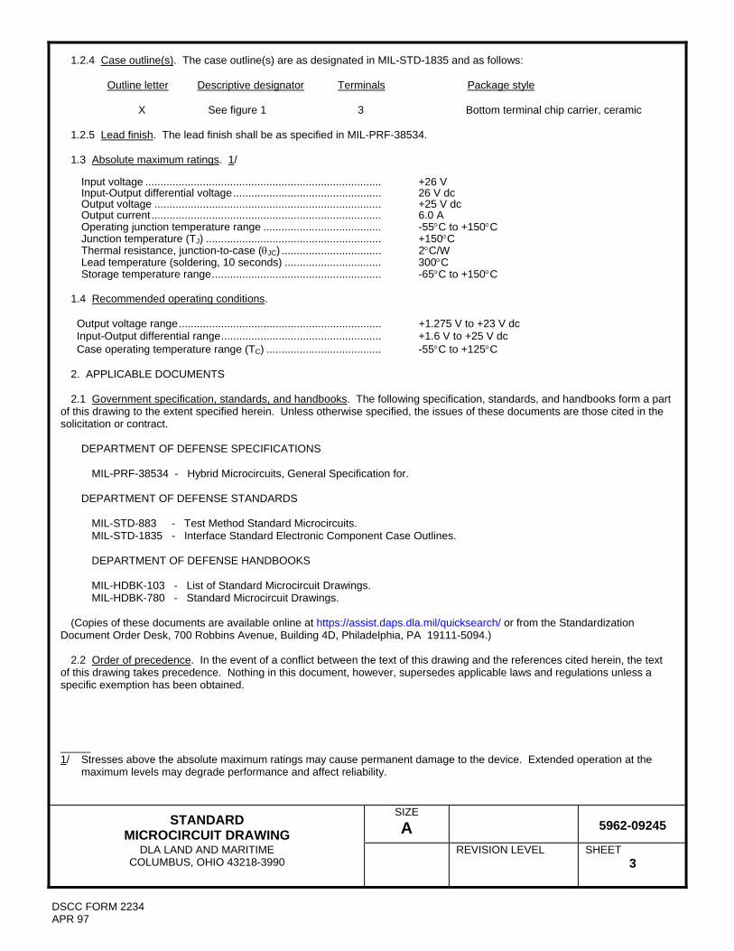
STANDARD MICROCIRCUIT DRAWING
SIZE A
5962-09245
DLA LAND AND MARITIME COLUMBUS, OHIO 43218-3990
REVISION LEVEL
SHEET 3
DSCC FORM 2234 APR 97
1.2.4 Case outline(s). The case outline(s) are as designated in MIL-STD-1835 and as follows:
Outline letter Descriptive designator Terminals Package style
X See figure 1 3 Bottom terminal chip carrier, ceramic
1.2.5 Lead finish. The lead finish shall be as specified in MIL-PRF-38534. 1.3 Absolute maximum ratings. 1/
Input voltage .............................................................................. +26 V Input-Output differential voltage ................................................. 26 V dc Output voltage ........................................................................... +25 V dc Output current ............................................................................ 6.0 A Operating junction temperature range ....................................... -55C to +150C Junction temperature (TJ) .......................................................... +150C Thermal resistance, junction-to-case (JC) ................................. 2C/W Lead temperature (soldering, 10 seconds) ................................ 300C Storage temperature range ........................................................ -65C to +150C
1.4 Recommended operating conditions.
Output voltage range ................................................................... +1.275 V to +23 V dc Input-Output differential range ..................................................... +1.6 V to +25 V dc Case operating temperature range (TC) ...................................... -55C to +125C
2. APPLICABLE DOCUMENTS
2.1 Government specification, standards, and handbooks. The following specification, standards, and handbooks form a part
of this drawing to the extent specified herein. Unless otherwise specified, the issues of these documents are those cited in the solicitation or contract.
DEPARTMENT OF DEFENSE SPECIFICATIONS
MIL-PRF-38534 - Hybrid Microcircuits, General Specification for.
DEPARTMENT OF DEFENSE STANDARDS
MIL-STD-883 - Test Method Standard Microcircuits. MIL-STD-1835 - Interface Standard Electronic Component Case Outlines.
DEPARTMENT OF DEFENSE HANDBOOKS
MIL-HDBK-103 - List of Standard Microcircuit Drawings. MIL-HDBK-780 - Standard Microcircuit Drawings.
(Copies of these documents are available online at https://assist.daps.dla.mil/quicksearch/ or from the Standardization Document Order Desk, 700 Robbins Avenue, Building 4D, Philadelphia, PA 19111-5094.)
2.2 Order of precedence. In the event of a conflict between the text of this drawing and the references cited herein, the text of this drawing takes precedence. Nothing in this document, however, supersedes applicable laws and regulations unless a specific exemption has been obtained. _____ 1/ Stresses above the absolute maximum ratings may cause permanent damage to the device. Extended operation at the maximum levels may degrade performance and affect reliability.

STANDARD MICROCIRCUIT DRAWING
SIZE A
5962-09245
DLA LAND AND MARITIME COLUMBUS, OHIO 43218-3990
REVISION LEVEL
SHEET 4
DSCC FORM 2234 APR 97
3. REQUIREMENTS
3.1 Item requirements. The individual item performance requirements for device classes D, E, G, H, and K shall be in accordance with MIL-PRF-38534. Compliance with MIL-PRF-38534 shall include the performance of all tests herein or as designated in the device manufacturer's Quality Management (QM) plan or as designated for the applicable device class. The manufacturer may eliminate, modify or optimize the tests and inspections herein, however the performance requirements as defined in MIL-PRF-38534 shall be met for the applicable device class. In addition, the modification in the QM plan shall not affect the form, fit, or function of the device for the applicable device class.
3.2 Design, construction, and physical dimensions. The design, construction, and physical dimensions shall be as specified in MIL-PRF-38534 and herein.
3.2.1 Case outline(s). The case outline(s) shall be in accordance with 1.2.4 herein and figure 1.
3.2.2 Terminal connections. The terminal connections shall be as specified on figure 2. 3.2.3 Block diagram. The block diagram shall be as specified on figure 3.
3.2.4 Maximum power dissipation verses case temperature chart. The maximum power dissipation verses case temperature is specified on figure 4.
3.3 Electrical performance characteristics. Unless otherwise specified herein, the electrical performance characteristics are as specified in table I and shall apply over the full specified operating temperature range.
3.4 Electrical test requirements. The electrical test requirements shall be the subgroups specified in table II. The electrical tests for each subgroup are defined in table I.
3.5 Marking of device(s). Marking of device(s) shall be in accordance with MIL-PRF-38534. The device shall be marked with the PIN listed in 1.2 herein. In addition, the manufacturer's vendor similar PIN may also be marked.
3.6 Data. In addition to the general performance requirements of MIL-PRF-38534, the manufacturer of the device described herein shall maintain the electrical test data (variables format) from the initial quality conformance inspection group A lot sample, for each device type listed herein. Also, the data should include a summary of all parameters manually tested, and for those which, if any, are guaranteed. This data shall be maintained under document revision level control by the manufacturer and be made available to the preparing activity DLA Land and Maritime-VA upon request.
3.7 Certificate of compliance. A certificate of compliance shall be required from a manufacturer in order to supply to this drawing. The certificate of compliance (original copy) submitted to DLA Land and Maritime-VA shall affirm that the manufacturer's product meets the performance requirements of MIL-PRF-38534 and herein.
3.8 Certificate of conformance. A certificate of conformance as required in MIL-PRF-38534 shall be provided with each lot of microcircuits delivered to this drawing.
4. VERIFICATION
4.1 Sampling and inspection. Sampling and inspection procedures shall be in accordance with MIL-PRF-38534 or as modified in the device manufacturer's Quality Management (QM) plan. The modification in the QM plan shall not affect the form, fit, or function as described herein.

STANDARD MICROCIRCUIT DRAWING
SIZE A
5962-09245
DLA LAND AND MARITIME COLUMBUS, OHIO 43218-3990
REVISION LEVEL
SHEET 5
DSCC FORM 2234 APR 97
TABLE I. Electrical performance characteristics.
Test
Symbol
Conditions
-55C TC +125C P PMAX, IOUT = 0.5 A
unless otherwise specified
Group A subgroups
Device types
Limits
Unit
Min
Max
Reference voltage
VREF
1.5 V (VIN - VOUT) 15 V, 10 mA IOUT 3.0 A
1,2,3
01
1.210
1.275
V
Line regulation 1/
ΔVOUT
ΔVIN
1.5 V (VIN - VOUT) 15 V, ILOAD = 10 mA, TJ = +25°C
1,2,3
01
0.25
%
Load regulation 1/
ΔVOUT
ΔIOUT
10 mA IOUT 3.0 A, (VIN - VOUT) = 3 V
1,2,3
01
0.40
%
Thermal regulation
30 ms pulse, TC = +25C
1
01
0.04
%/W
Dropout voltage
VDROP
VREF = 1%, IOUT = 3.0 A
1,2,3
01
1.60
V
Ripple rejection
IOUT = 3.0 A, (VIN - VOUT) = 3 V, f = 120 Hz, CADJ = COUT = 25 F
1,2,3
01
60
dB
Adjustment pin current
IADJ
TC = +25C
1
01
120
A
Adjustment pin current change
IADJ
10 mA IOUT 3.0 A, 1.5 V (VIN - VOUT) 15 V
1,2,3
01
5
A
Minimum load current 2/
IMIN
(VIN - VOUT) = 25 V
1,2,3
01
10
mA
Current limit
IMAX
(VIN - VOUT) 5 V
1,2,3
01
5.25
A
VREF Long term stability 3/
ΔVOUT
ΔTIME
Burn-in: TC = +125C at 1000 hours minimum, tested at +25C
1
01
1.0
%
1/ Regulation is measured at a constant junction temperature, using pulse testing with a low duty cycle. Changes in output voltage due to heating effects are covered under the specification for thermal regulation. Measurements taken at the output lead must be adjusted for lead resistance. 2/ Guaranteed by design. 3/ Not tested. Parameter shall be guaranteed to the specified limits after 1000 hour life test.

STANDARD MICROCIRCUIT DRAWING
SIZE A
5962-09245
DLA LAND AND MARITIME COLUMBUS, OHIO 43218-3990
REVISION LEVEL
SHEET 6
DSCC FORM 2234 APR 97
Case X
FIGURE 1. Case outline(s).

STANDARD MICROCIRCUIT DRAWING
SIZE A
5962-09245
DLA LAND AND MARITIME COLUMBUS, OHIO 43218-3990
REVISION LEVEL
SHEET 7
DSCC FORM 2234 APR 97
Case X - Continued.
Symbol Inches Millimeters
Min Max Min Max
A .127 3.23
A1 .010 .020 .25 .51
b .281 .291 7.14 7.39
b1 .220 .230 5.59 5.84
b2 .090 .100 2.29 2.54
b3 .115 .125 2.92 3.18
D .405 10.29
D1 .030 7.62
E .301 7.65
e .030 7.62
R .015 .025 .38 .64
S .010 .25
NOTE: 1. The U.S. preferred system of measurement is the metric SI. This item was designed using inch-pound units of measurement. In case of problems involving conflicts between the metric and inch-pound units, the inch-pound units shall rule. 2 The package and lid are electrically isolated from signal pads.
FIGURE 1. Case outline(s) - Continued.

STANDARD MICROCIRCUIT DRAWING
SIZE A
5962-09245
DLA LAND AND MARITIME COLUMBUS, OHIO 43218-3990
REVISION LEVEL
SHEET 8
DSCC FORM 2234 APR 97
Device type 01 Case outline X
Terminal number Terminal symbol
1 2 3
VOUT VIN ADJ
FIGURE 2. Terminal connections.
FIGURE 3. Block diagram.

STANDARD MICROCIRCUIT DRAWING
SIZE A
5962-09245
DLA LAND AND MARITIME COLUMBUS, OHIO 43218-3990
REVISION LEVEL
SHEET 9
DSCC FORM 2234 APR 97
Case
Temperature (C)
Maximum power
dissipation (Watts)
0 75.0 5 72.0
10 70.0 15 67.5 20 65.0 25 62.5 30 60.0 35 57.5 40 55.0 45 52.5 50 50.0 55 47.5 60 45.0 65 42.5 70 40.0 75 37.5 80 35.0 85 32.5 90 30.0 95 27.5
100 25.0 105 22.5 110 20.0 115 17.5 120 15.0 125 12.5 130 10.0 135 7.5 140 5.0 145 2.5 150 0.0
FIGURE 4. Maximum power dissipation verses case temperature chart.

STANDARD MICROCIRCUIT DRAWING
SIZE A
5962-09245
DLA LAND AND MARITIME COLUMBUS, OHIO 43218-3990
REVISION LEVEL
SHEET 10
DSCC FORM 2234 APR 97
TABLE II. Electrical test requirements.
MIL-PRF-38534 test requirements Subgroups
(in accordance with MIL-PRF-38534, group A
test table) Interim electrical parameters
1,2,3
Final electrical parameters
1*,2,3
Group A test requirements
1,2,3
Group C end-point electrical parameters
1,2,3
End-point electrical parameters for Radiation Hardness Assurance (RHA) devices
Not applicable
* PDA applies to subgroup 1.
4.2 Screening. Screening shall be in accordance with MIL-PRF-38534. The following additional criteria shall apply:
a. Burn-in test, method 1015 of MIL-STD-883.
(1) Test condition A, B, C, or D. The test circuit shall be maintained by the manufacturer under document revision level control and shall be made available to either DLA Land and Maritime-VA or the acquiring activity upon request. Also, the test circuit shall specify the inputs, outputs, biases, and power dissipation, as applicable, in accordance with the intent specified in method 1015 of MIL-STD-883.
(2) TC as specified in accordance with table I of method 1015 of MIL-STD-883.
b. Interim and final electrical test parameters shall be as specified in table II herein, except interim electrical parameter
tests prior to burn-in are optional at the discretion of the manufacturer.
4.3 Conformance and periodic inspections. Conformance inspection (CI) and periodic inspection (PI) shall be in accordance with MIL-PRF-38534 and as specified herein.
4.3.1 Group A inspection (CI). Group A inspection shall be in accordance with MIL-PRF-38534 and as follows:
a. Tests shall be as specified in table II herein.
b. Subgroups 4, 5, 6, 7, 8A, 8B, 9, 10, and 11 shall be omitted.
4.3.2 Group B inspection (PI). Group B inspection shall be in accordance with MIL-PRF-38534.

STANDARD MICROCIRCUIT DRAWING
SIZE A
5962-09245
DLA LAND AND MARITIME COLUMBUS, OHIO 43218-3990
REVISION LEVEL
SHEET 11
DSCC FORM 2234 APR 97
4.3.3 Group C inspection (PI). Group C inspection shall be in accordance with MIL-PRF-38534 and as follows:
a. End-point electrical parameters shall be as specified in table II herein.
b. Steady-state life test, method 1005 of MIL-STD-883.
(1) Test condition A, B, C, or D. The test circuit shall be maintained by the manufacturer under document revision level control and shall be made available to either DLA Land and Maritime-VA or the acquiring activity upon request. Also, the test circuit shall specify the inputs, outputs, biases, and power dissipation, as applicable, in accordance with the intent specified in method 1005 of MIL-STD-883.
(2) TC as specified in accordance with table I of method 1005 of MIL-STD-883.
(3) Test duration: 1,000 hours, except as permitted by method 1005 of MIL-STD-883.
4.3.4 Group D inspection (PI). Group D inspection shall be in accordance with MIL-PRF-38534.
4.3.5 Radiation Hardness Assurance (RHA) inspection. RHA inspection is not currently applicable to this drawing.
5. PACKAGING
5.1 Packaging requirements. The requirements for packaging shall be in accordance with MIL-PRF-38534.
6. NOTES
6.1 Intended use. Microcircuits conforming to this drawing are intended for use for Government microcircuit applications
(original equipment), design applications, and logistics purposes. 6.2 Replaceability. Microcircuits covered by this drawing will replace the same generic device covered by a contractor-prepared specification or drawing.
6.3 Configuration control of SMD's. All proposed changes to existing SMD's will be coordinated as specified in MIL-PRF-
38534. 6.4 Record of users. Military and industrial users shall inform DLA Land and Maritime when a system application requires
configuration control and the applicable SMD. DLA Land and Maritime will maintain a record of users and this list will be used for coordination and distribution of changes to the drawings. Users of drawings covering microelectronic devices (FSC 5962) should contact DLA Land and Maritime-VA, telephone (614) 692-0544.
6.5 Comments. Comments on this drawing should be directed to DLA Land and Maritime-VA, Columbus, Ohio 43218-3990,
or telephone (614) 692-1081.
6.6 Sources of supply. Sources of supply are listed in MIL-HDBK-103 and QML-38534. The vendors listed in MIL-HDBK-103 and QML-38534 have submitted a certificate of compliance (see 3.7 herein) to DLA Land and Maritime-VA and have agreed to this drawing.

STANDARD MICROCIRCUIT DRAWING BULLETIN DATE: Approved sources of supply for SMD 5962-09245 are listed below for immediate acquisition information only and shall be added to MIL-HDBK-103 and QML-38534 during the next revisions. MIL-HDBK-103 and QML-38534 will be revised to include the addition or deletion of sources. The vendors listed below have agreed to this drawing and a certificate of compliance has been submitted to and accepted by DLA Land and Maritime-VA. This information bulletin is superseded by the next dated revisions of MIL-HDBK-103 and QML-38534. DLA Land and Maritime maintains an online database of all current sources of supply at http://www.dscc.dla.mil/Programs/Smcr/.
Standard
microcircuit drawing PIN 1/
Vendor CAGE
number
Vendor similar PIN 2/
5962-0924501KXA 5962-0924501KXC
88379 88379
VRG8684-201-2S VRG8684-201-1S
1/ The lead finish shown for each PIN representing
a hermetic package is the most readily available from the manufacturer listed for that part. If the desired lead finish is not listed contact the Vendor to determine its availability.
2/ Caution. Do not use this number for item acquisition. Items acquired to this number may not satisfy the performance requirements of this drawing.
Vendor CAGE Vendor name number and address
88379 Aeroflex Plainview Incorporated, (Aeroflex Microelectronics Solutions)
35 South Service Road Plainview, NY 11803-4193
The information contained herein is disseminated for convenience only and the Government assumes no liability whatsoever for any inaccuracies in the information bulletin.

REVISIONS
LTR DESCRIPTION DATE (YR-MO-DA) APPROVED
"PRELIMINARY DRAFT 11-18-10" REV
SHEET
REV
SHEET 15 16
REV STATUS REV OF SHEETS SHEET 1 2 3 4 5 6 7 8 9 10 11 12 13 14
PMIC N/A
PREPARED BY Steve Duncan
DLA LAND AND MARITIME COLUMBUS, OHIO 43218-3990
http://www.dscc.dla.mil/
STANDARD MICROCIRCUIT DRAWING
CHECKED BY Greg Cecil
THIS DRAWING IS AVAILABLE
FOR USE BY ALL DEPARTMENTS
AND AGENCIES OF THE DEPARTMENT OF DEFENSE
APPROVED BY Charles F. Saffle
MICROCIRCUIT, HYBRID, DUAL VOLTAGE REGULATOR, 3 AMP, POSITIVE AND NEGATIVE, LOW DROPOUT, ADJUSTABLE
DRAWING APPROVAL DATE
AMSC N/A
REVISION LEVEL
SIZE A
CAGE CODE 67268
5962-10213
SHEET 1 OF
15
DSCC FORM 2233 APR 97 5962-E166-10

STANDARD MICROCIRCUIT DRAWING
SIZE A
5962-10213
DLA LAND AND MARITIME COLUMBUS, OHIO 43218-3990
REVISION LEVEL
SHEET 2
DSCC FORM 2234 APR 97
1. SCOPE
1.1 Scope. This drawing documents five product assurance classes as defined in paragraph 1.2.3 and MIL-PRF-38534. A choice of case outlines and lead finishes which are available and are reflected in the Part or Identifying Number (PIN). When available, a choice of radiation hardness assurance levels are reflected in the PIN.
1.2 PIN. The PIN shall be as shown in the following example:
5962 - 10213 01 K U X
Federal RHA Device Device Case Lead stock class designator type class outline finish designator (see 1.2.1) (see 1.2.2) designator (see 1.2.4) (see 1.2.5)
\ / (see 1.2.3) \/ Drawing number
1.2.1 Radiation hardness assurance (RHA) designator. RHA marked devices shall meet the MIL-PRF-38534 specified RHA
levels and shall be marked with the appropriate RHA designator. A dash (-) indicates a non-RHA device.
1.2.2 Device type(s). The device type(s) identify the circuit function as follows:
Device type Generic number Circuit function
01 8653, 8654 Dual voltage regulator, 3 amp, positive and negative, low dropout, adjustable
02 8687, 8688 Dual voltage regulator, 3 amp, positive, low dropout adjustable
1.2.3 Device class designator. This device class designator shall be a single letter identifying the product assurance level. All levels are defined by the requirements of MIL-PRF-38534 and require QML Certification as well as qualification (Class H, K, and E) or QML Listing (Class G and D). The product assurance levels are as follows:
Device class Device performance documentation
K Highest reliability class available. This level is intended for use in space applications. H Standard military quality class level. This level is intended for use in applications
where non-space high reliability devices are required. G Reduced testing version of the standard military quality class. This level uses the
Class H screening and In-Process Inspections with a possible limited temperature range, manufacturer specified incoming flow, and the manufacturer guarantees (but may not test) periodic and conformance inspections (Group A, B, C and D).
E Designates devices which are based upon one of the other classes (K, H, or G)
with exception(s) taken to the requirements of that class. These exception(s) must be specified in the device acquisition document; therefore the acquisition document should be reviewed to ensure that the exception(s) taken will not adversely affect system performance.
D Manufacturer specified quality class. Quality level is defined by the manufacturers internal, QML certified flow. This product may have a limited temperature range.

STANDARD MICROCIRCUIT DRAWING
SIZE A
5962-10213
DLA LAND AND MARITIME COLUMBUS, OHIO 43218-3990
REVISION LEVEL
SHEET 3
DSCC FORM 2234 APR 97
1.2.4 Case outline(s). The case outline(s) are as designated in MIL-STD-1835 and as follows:
Outline letter Descriptive designator Terminals Package style
U See figure 1 8 Thru-hole Z See figure 1 8 Surface Mount
1.2.5 Lead finish. The lead finish shall be as specified in MIL-PRF-38534. 1.3 Absolute maximum ratings. 1/
Input voltage: Positive regulator .................................................................... +26 V Negative regulator .................................................................. -35 V Input-Output differential voltage: Positive regulator .................................................................... 26 V Negative regulator .................................................................. 30 V Output voltage: Positive regulator .................................................................... +25 V Negative regulator .................................................................. -30 V Output current: Positive regulator .................................................................... 6 A Junction temperature (TJ) .......................................................... +150C Power Dissipation (PD) ............................................................... See table IA herein Thermal resistance, junction-to-case (JC) each regulator ......... 5C/W Lead temperature (soldering, 10 seconds) ................................ 300C Storage temperature range ........................................................ -65C to +150C
1.4 Recommended operating conditions.
Output voltage range: Postive voltage regulator ....................................................... +1.275 V to +23 V dc Negative voltage regulator ...................................................... -2.45 V to -25 V dc Input- Output differential range Positive regulator .................................................................... +1.6 V to +25 V Negative regulator .................................................................. -1 V to -28 V Output current: Positive regulator .................................................................... 3 A maximum Neagtive regulator .................................................................. 3 A maximum Case operating temperature range (TC) ...................................... -55C to +125C
2. APPLICABLE DOCUMENTS
2.1 Government specification, standards, and handbooks. The following specification, standards, and handbooks form a part
of this drawing to the extent specified herein. Unless otherwise specified, the issues of these documents are those cited in the solicitation or contract.
DEPARTMENT OF DEFENSE SPECIFICATIONS
MIL-PRF-38534 - Hybrid Microcircuits, General Specification for. ________ 1/ Stresses above the absolute maximum ratings may cause permanent damage to the device. Extended operation at the maximum levels may degrade performance and affect reliability.

STANDARD MICROCIRCUIT DRAWING
SIZE A
5962-10213
DLA LAND AND MARITIME COLUMBUS, OHIO 43218-3990
REVISION LEVEL
SHEET 4
DSCC FORM 2234 APR 97
DEPARTMENT OF DEFENSE STANDARDS
MIL-STD-883 - Test Method Standard Microcircuits. MIL-STD-1835 - Interface Standard Electronic Component Case Outlines.
MIL-HDBK-103 - List of Standard Microcircuit Drawings.
MIL-HDBK-780 - Standard Microcircuit Drawings. (Copies of these documents are available online at https://assist.daps.dla.mil/quicksearch/ or from the Standardization Document Order Desk, 700 Robbins Avenue, Building 4D, Philadelphia, PA 19111-5094.)
2.2 Order of precedence. In the event of a conflict between the text of this drawing and the references cited herein, the text of this drawing takes precedence. Nothing in this document, however, supersedes applicable laws and regulations unless a specific exemption has been obtained.
3. REQUIREMENTS
3.1 Item requirements. The individual item performance requirements for device classes D, E, G, H, and K shall be in accordance with MIL-PRF-38534. Compliance with MIL-PRF-38534 shall include the performance of all tests herein or as designated in the device manufacturer's Quality Management (QM) plan or as designated for the applicable device class. The manufacturer may eliminate, modify or optimize the tests and inspections herein, however the performance requirements as defined in MIL-PRF-38534 shall be met for the applicable device class. In addition, the modification in the QM plan shall not affect the form, fit, or function of the device for the applicable device class.
3.2 Design, construction, and physical dimensions. The design, construction, and physical dimensions shall be as specified in MIL-PRF-38534 and herein.
3.2.1 Case outline(s). The case outline(s) shall be in accordance with 1.2.4 herein and figure 1.
3.2.2 Terminal connections. The terminal connections shall be as specified on figure 2. 3.2.3 Block diagram. The block diagram shall be as specified on figure 3.
3.2.4 Maximum power dissipation verses case temperature table. The maximum power dissipation verses case temperature
is specified in table IA.
3.3 Electrical performance characteristics. Unless otherwise specified herein, the electrical performance characteristics are as specified in table I and shall apply over the full specified operating temperature range.
3.4 Electrical test requirements. The electrical test requirements shall be the subgroups specified in table II. The electrical tests for each subgroup are defined in table I.
3.5 Marking of device(s). Marking of device(s) shall be in accordance with MIL-PRF-38534. The device shall be marked with the PIN listed in 1.2 herein. In addition, the manufacturer's vendor similar PIN may also be marked.
3.6 Data. In addition to the general performance requirements of MIL-PRF-38534, the manufacturer of the device described herein shall maintain the electrical test data (variables format) from the initial quality conformance inspection group A lot sample, for each device type listed herein. Also, the data should include a summary of all parameters manually tested, and for those which, if any, are guaranteed. This data shall be maintained under document revision level control by the manufacturer and be made available to the preparing activity (DLA Land and Maritime -VA) upon request.
3.7 Certificate of compliance. A certificate of compliance shall be required from a manufacturer in order to supply to this drawing. The certificate of compliance (original copy) submitted to DLA Land and Maritime -VA shall affirm that the manufacturer's product meets the performance requirements of MIL-PRF-38534 and herein.
3.8 Certificate of conformance. A certificate of conformance as required in MIL-PRF-38534 shall be provided with each lot of microcircuits delivered to this drawing.

STANDARD MICROCIRCUIT DRAWING
SIZE A
5962-10213
DLA LAND AND MARITIME COLUMBUS, OHIO 43218-3990
REVISION LEVEL
SHEET 5
DSCC FORM 2234 APR 97
TABLE I. Electrical performance characteristics.
Test
Symbol
Conditions
-55C TC +125C P PMAX
unless otherwise specified
Group A subgroups
Device types
Limits
Unit
Min
Max
POSITIVE REGULATOR Reference voltage
VREF
1.5 V (VIN - VOUT) 15 V, ILOAD = 10 mA
1,2,3
01,02
1.210
1.275
V
Line regulation 1/
ΔVOUT
ΔVIN
1.5 V (VIN - VOUT) 15 V, ILOAD = 10 mA
1,2,3
01,02
0.25
%
Load regulation 1/
ΔVOUT
ΔIOUT
10 mA IOUT 3.0 A, (VIN - VOUT) = 3 V
4,5,6
01,02
0.40
%
Thermal regulation
30 ms pulse, TC = +25C
4
01,02
0.04
%/W
Dropout voltage
VDROP
VREF = 1%, IOUT = 3.0 A
9,10,11
01,02
1.60
V
Ripple rejection
IOUT = 3.0 A, (VIN - VOUT) = 3 V, f = 120 Hz, CADJ = COUT = 25 F
9,10,11
01,02
60
dB
Adjustment pin current
IADJ
1,2,3
01,02
120
A
Adjustment pin current change
IADJ
10 mA IOUT 3.0 A, 1.5 V (VIN - VOUT) 15 V
1,2,3
01,02
5
A
Minimum load current 2/
IMIN
(VIN - VOUT) = 25V
1,2,3
01,02
10
mA
VREF Long term stability 2/
ΔVOUT
ΔTIME
Burn-in: TC = +125C at 1000 hours minimum, tested at +25C
1
01,02
1.0
%
Current limit
ICL
(VIN - VOUT) = 5 V
4
01,02
5.25
A
NEGATIVE REGULATOR Reference voltage
VREF
VIN - VOUT = -1.2 V to -28 V, 1 mA IOUT 3 A, VOUT = -5 V
1,2,3
01
-2.29
-2.45
V
See footnotes at end of table.

STANDARD MICROCIRCUIT DRAWING
SIZE A
5962-10213
DLA LAND AND MARITIME COLUMBUS, OHIO 43218-3990
REVISION LEVEL
SHEET 6
DSCC FORM 2234 APR 97
TABLE I. Electrical performance characteristics - Continued.
Test
Symbol
Conditions
-55C TC +125C P PMAX
unless otherwise specified
Group A subgroups
Device types
Limits
Unit
Min
Max
NEGATIVE REGULATOR - CONTINUED Dropout Voltage
VDROP
IOUT = 0.5 A, VOUT = -5 V
9,10,11
01
0.425
V
IOUT = 3 A, VOUT = -5 V
1.05
Ripple rejection
IOUT = 1.0 A, (VIN - VOUT) = 3 V, f = 120 Hz, CADJ = COUT = 25 F
9,10,11
01
60
dB
Line regulation 1/
ΔVOUT
ΔVIN
1 V VIN - VOUT) 20V, VOUT = -5 V
1,2,3
01
0.02
%/V
Load regulation 1/
ΔVOUT
ΔIOUT
5 mA IOUT 3 A, (VIN - VOUT) = -15 V to -10 V, VOUT = -5 V
4,5,6
01
0.8
%
Thermal regulation 2/
VIN - VOUT = 10 V, IOUT = 5 mA to 2 A, TC = +25C
4
01
0.014
%/W
Minimum input voltage
VIN MIN
IOUT = 3 A, VOUT = VREF
9,10,11
01
-4.5
V
Internal current limit
IMAX
-1.5 V (VIN - VOUT) -10 V, TC = +25C
4
01
3.3
4.55
A
(VIN - VOUT) =-15 V, TC = +25C
2.0
4.5
(VIN - VOUT) -20 V, TC = +25
1.0
3.1
(VIN - VOUT) = -30 V, 2/ TC = +25C and -55C
0.2
1.6
External current limit
ILIM
RLIM = 5 k
4,5,6
01
2.7
3.7
A
RLIM = 15 k
0.9
1.6
See footnotes at end of table.

STANDARD MICROCIRCUIT DRAWING
SIZE A
5962-10213
DLA LAND AND MARITIME COLUMBUS, OHIO 43218-3990
REVISION LEVEL
SHEET 7
DSCC FORM 2234 APR 97
TABLE I. Electrical performance characteristics - Continued.
Test
Symbol
Conditions
-55°C TC +125C P PMAX
unless otherwise specified
Group A subgroups
Device types
Limits
Unit
Min
Max
NEGATIVE REGULATOR - CONTINUED Quiescent supply current
IQ
IOUT = 5 mA, VOUT = VREF, (-4 V VIN -25 V)
1,2,3
01
3.5
mA
Supply current change with load
IQ
(VIN - VOUT) = .25 V +(.25 x IOUT)
1,2,3
01
35
mA/A
(VIN - VOUT) -2 V
21
1/ Regulation is measured at a constant junction temperature, using pulse testing with a low duty cycle. Changes in output voltage due to heating effects are covered under the specification for thermal regulation. Measurements taken at the output lead must be adjusted for lead resistance. 2/ Parameter shall be tested at intial device characterization and after design or process changes. Parameter shall be guaranteed to the limits specified in table I for all lots not specifically tested.
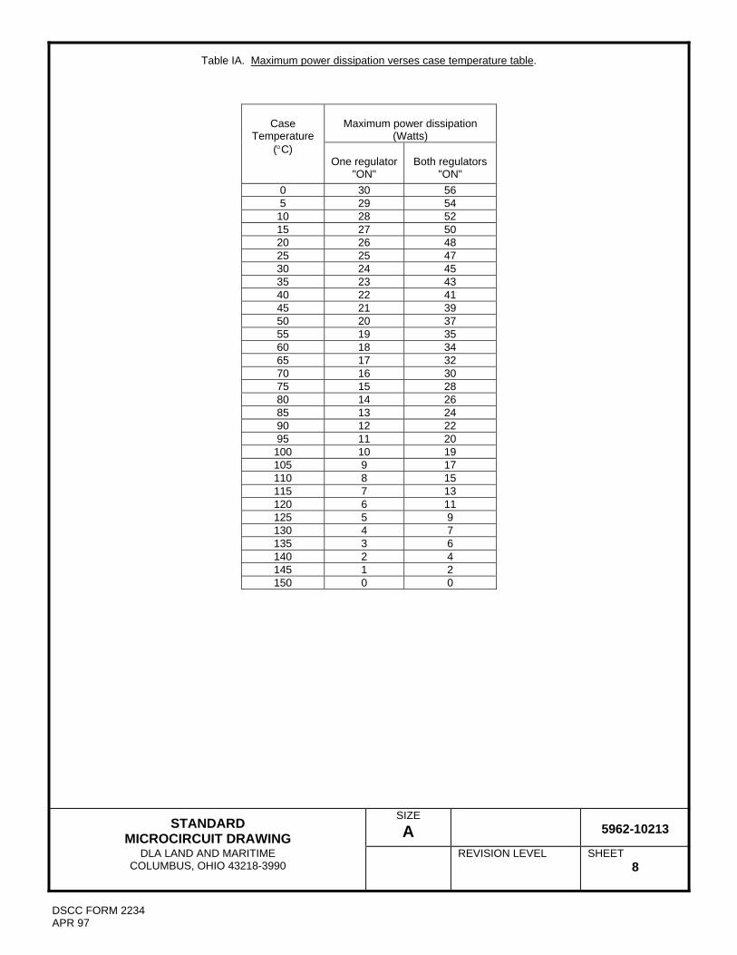
STANDARD MICROCIRCUIT DRAWING
SIZE A
5962-10213
DLA LAND AND MARITIME COLUMBUS, OHIO 43218-3990
REVISION LEVEL
SHEET 8
DSCC FORM 2234 APR 97
Table IA. Maximum power dissipation verses case temperature table.
Case
Temperature (C)
Maximum power dissipation
(Watts)
One regulator "ON"
Both regulators
"ON" 0 30 56 5 29 54
10 28 52 15 27 50 20 26 48 25 25 47 30 24 45 35 23 43 40 22 41 45 21 39 50 20 37 55 19 35 60 18 34 65 17 32 70 16 30 75 15 28 80 14 26 85 13 24 90 12 22 95 11 20
100 10 19 105 9 17 110 8 15 115 7 13 120 6 11 125 5 9 130 4 7 135 3 6 140 2 4 145 1 2 150 0 0

STANDARD MICROCIRCUIT DRAWING
SIZE A
5962-10213
DLA LAND AND MARITIME COLUMBUS, OHIO 43218-3990
REVISION LEVEL
SHEET 9
DSCC FORM 2234 APR 97
Case U
FIGURE 1. Case outline(s).

STANDARD MICROCIRCUIT DRAWING
SIZE A
5962-10213
DLA LAND AND MARITIME COLUMBUS, OHIO 43218-3990
REVISION LEVEL
SHEET 10
DSCC FORM 2234 APR 97
Case U - Continued.
Symbol Inches Millimeters
Min Max Min Max
A .220 5.59
b .028 .032 0.71 0.81
b3 .085 .095 2.12 2.41
D .750 .760 19.05 19.30
D1 .510 .520 12.95 13.21
e .100 BSC 2.54 BSC
e1 .300 BSC 7.62 BSC
e2 .108 BSC 2.74 BSC
eA .700 .740 17.78 18.80
E .410 .420 10.41 10.67
F .035 .045 0.90 1.14
G1 .632 BSC 16.05 BSC
G2 .2025 .2125 5.144 5.408
L1 .230 5.84
L2 .150 REF 3.81 REF
p .140 .150 3.56 3.81
Q .122 TYP 3.10 TYP
R .065 TYP 1.65 TYP
S1 .028 0.71
NOTES: 1. The U.S. preferred system of measurement is the metric SI. This item was designed using inch-pound units of measurement. In case of problems involving conflicts between the metric and inch-pound units, the inch-pound units shall rule. 2. The package contains a BeO substrate. 3. The case is electrically isolated.
FIGURE 1. Case outline(s) - Continued.

STANDARD MICROCIRCUIT DRAWING
SIZE A
5962-10213
DLA LAND AND MARITIME COLUMBUS, OHIO 43218-3990
REVISION LEVEL
SHEET 11
DSCC FORM 2234 APR 97
Case Z
FIGURE 1. Case outlines(s) - Continued.

STANDARD MICROCIRCUIT DRAWING
SIZE A
5962-10213
DLA LAND AND MARITIME COLUMBUS, OHIO 43218-3990
REVISION LEVEL
SHEET 12
DSCC FORM 2234 APR 97
Case Z - Continued.
Symbol Inches Millimeters
Min Max Min Max
A .220 5.59
A1 .015 .025 0.38 0.64
b .028 .032 0.71 0.81
b3 .085 .095 2.12 2.41
D .750 .760 19.05 19.30
D1 .510 .520 12.95 13.21
e .100 BSC 2.54 BSC
e1 .300 BSC 7.62 BSC
e2 .108 BSC 2.74 BSC
E .410 .420 10.41 10.67
F .035 .045 0.90 1.14
G1 .632 BSC 16.05 BSC
G2 .2025 .2125 5.144 5.408
H .866 .906 22.00 23.01
L1 .055 .065 1.40 1.65
L2 .150 REF 3.81 REF
p .140 .150 3.56 3.81
Q .122 TYP 3.10 TYP
R .065 TYP 1.65 TYP
S1 .028 0.71
NOTES: 1. The U.S. preferred system of measurement is the metric SI. This item was designed using inch-pound units of measurement. In case of problems involving conflicts between the metric and inch-pound units, the inch-pound units shall rule. 2. The package contains a BeO substrate. 3. The case is electrically isolated.
FIGURE 1. Case outline(s) - Continued.

STANDARD MICROCIRCUIT DRAWING
SIZE A
5962-10213
DLA LAND AND MARITIME COLUMBUS, OHIO 43218-3990
REVISION LEVEL
SHEET 13
DSCC FORM 2234 APR 97
Device types 01 02 Case outlines U and Z
Terminal number Terminal symbol Terminal symbol
1 2 3 4 5 6 7 8
POS_ ADJ_1 NEG_REF_2 NEG_VOUT_2 NEG_VIN_2
NEG_GND_2 NEG_FB_2
POS_VOUT_1 POS_VIN_1
ADJ_1 VOUT_1
SENSE_1 VIN_2 ADJ_2 VOUT_2
SENSE_2 VIN_1
FIGURE 2. Terminal connections.
FIGURE 3. Block diagram.

STANDARD MICROCIRCUIT DRAWING
SIZE A
5962-10213
DLA LAND AND MARITIME COLUMBUS, OHIO 43218-3990
REVISION LEVEL
SHEET 14
DSCC FORM 2234 APR 97
FIGURE 3. Block diagram - Continued.

STANDARD MICROCIRCUIT DRAWING
SIZE A
5962-10213
DLA LAND AND MARITIME COLUMBUS, OHIO 43218-3990
REVISION LEVEL
SHEET 15
DSCC FORM 2234 APR 97
TABLE II. Electrical test requirements.
MIL-PRF-38534 test requirements Subgroups
(in accordance with MIL-PRF-38534, group A
test table) Interim electrical parameters
1,2,3,4,5,6,9,10,11
Final electrical parameters
1*,2,3,4,5,6,9,10,11
Group A test requirements
1,2,3,4,5,6,9,10,11
Group C end-point electrical parameters
1,2,3,4,5,6,9,10,11
End-point electrical parameters for Radiation Hardness Assurance (RHA) devices
Not applicable
* PDA applies to subgroup 1.
4. VERIFICATION
4.1 Sampling and inspection. Sampling and inspection procedures shall be in accordance with MIL-PRF-38534 or as
modified in the device manufacturer's Quality Management (QM) plan. The modification in the QM plan shall not affect the form, fit, or function as described herein. 4.2 Screening. Screening shall be in accordance with MIL-PRF-38534. The following additional criteria shall apply:
a. Burn-in test, method 1015 of MIL-STD-883.
(1) Test condition A, B, C, or D. The test circuit shall be maintained by the manufacturer under document revision level control and shall be made available to either DLA Land and Maritime -VA or the acquiring activity upon request. Also, the test circuit shall specify the inputs, outputs, biases, and power dissipation, as applicable, in accordance with the intent specified in method 1015 of MIL-STD-883.
(2) TA as specified in accordance with table I of method 1015 of MIL-STD-883.
b. Interim and final electrical test parameters shall be as specified in table II herein, except interim electrical parameter
tests prior to burn-in are optional at the discretion of the manufacturer.
4.3 Conformance and periodic inspections. Conformance inspection (CI) and periodic inspection (PI) shall be in accordance with MIL-PRF-38534 and as specified herein.
4.3.1 Group A inspection (CI). Group A inspection shall be in accordance with MIL-PRF-38534 and as follows:
a. Tests shall be as specified in table II herein.
b. Subgroups 7, 8A, and 8B shall be omitted.
4.3.2 Group B inspection (PI). Group B inspection shall be in accordance with MIL-PRF-38534.

STANDARD MICROCIRCUIT DRAWING
SIZE A
5962-10213
DLA LAND AND MARITIME COLUMBUS, OHIO 43218-3990
REVISION LEVEL
SHEET 16
DSCC FORM 2234 APR 97
4.3.3 Group C inspection (PI). Group C inspection shall be in accordance with MIL-PRF-38534 and as follows:
a. End-point electrical parameters shall be as specified in table II herein.
b. Steady-state life test, method 1005 of MIL-STD-883.
(1) Test condition A, B, C, or D. The test circuit shall be maintained by the manufacturer under document revision level control and shall be made available to either DLA Land and Maritime -VA or the acquiring activity upon request. Also, the test circuit shall specify the inputs, outputs, biases, and power dissipation, as applicable, in accordance with the intent specified in method 1005 of MIL-STD-883.
(2) TA as specified in accordance with table I of method 1005 of MIL-STD-883.
(3) Test duration: 1,000 hours, except as permitted by method 1005 of MIL-STD-883.
4.3.4 Group D inspection (PI). Group D inspection shall be in accordance with MIL-PRF-38534.
4.3.5 Radiation Hardness Assurance (RHA) inspection. RHA inspection is not currently applicable to this drawing.
5. PACKAGING
5.1 Packaging requirements. The requirements for packaging shall be in accordance with MIL-PRF-38534.
6. NOTES
6.1 Intended use. Microcircuits conforming to this drawing are intended for use for Government microcircuit applications
(original equipment), design applications, and logistics purposes. 6.2 Replaceability. Microcircuits covered by this drawing will replace the same generic device covered by a contractor-prepared specification or drawing.
6.3 Configuration control of SMD's. All proposed changes to existing SMD's will be coordinated as specified in MIL-PRF-
38534. 6.4 Record of users. Military and industrial users shall inform DLA Land and Maritime -VA when a system application
requires configuration control and the applicable SMD. DLA Land and Maritime -VA will maintain a record of users and this list will be used for coordination and distribution of changes to the drawings. Users of drawings covering microelectronic devices (FSC 5962) should contact DLA Land and Maritime -VA, telephone (614) 692-0544.
6.5 Comments. Comments on this drawing should be directed to DLA Land and Maritime -VA, Columbus, Ohio 43218-3990,
or telephone (614) 692-1081.
6.6 Sources of supply. Sources of supply are listed in MIL-HDBK-103 and QML-38534. The vendors listed in MIL-HDBK-103 and QML-38534 have submitted a certificate of compliance (see 3.7 herein) to DLA Land and Maritime -VA and have agreed to this drawing.

STANDARD MICROCIRCUIT DRAWING BULLETIN DATE: Approved sources of supply for SMD 5962-10213 are listed below for immediate acquisition information only and shall be added to MIL-HDBK-103 and QML-38534 during the next revisions. MIL-HDBK-103 and QML-38534 will be revised to include the addition or deletion of sources. The vendors listed below have agreed to this drawing and a certificate of compliance has been submitted to and accepted by DLA Land and Maritime -VA. This information bulletin is superseded by the next dated revisions of MIL-HDBK-103 and QML-38534. DLA Land and Maritime maintains an online database of all current sources of supply at http://www.dscc.dla.mil/Programs/Smcr/.
Standard
microcircuit drawing PIN 1/
Vendor CAGE
number
Vendor similar PIN 2/
5962-1021301KUA 5962-1021301KUC 5962-1021301KZA 5962-1021301KZC
88379 88379 88379 88379
VRG8653-201-2S VRG8653-201-1S VRG8654-201-2S VRG8654-201-1S
5962-1021302KUA 5962-1021302KUC 5962-1021302KZA 5962-1021302KZC
88379 88379 88379 88379
VRG8687-201-2S VRG8687-201-1S VRG8688-201-2S VRG8688-201-1S
1/ The lead finish shown for each PIN representing
a hermetic package is the most readily available from the manufacturer listed for that part. If the desired lead finish is not listed contact the Vendor to determine its availability.
2/ Caution. Do not use this number for item acquisition. Items acquired to this number may not satisfy the performance requirements of this drawing.
Vendor CAGE Vendor name number and address
88379 Aeroflex Plainview Incorporated, (Aeroflex Microelectronics Solutions)
35 South Service Road Plainview, NY 11803-4193
The information contained herein is disseminated for convenience only and the Government assumes no liability whatsoever for any inaccuracies in the information bulletin.

REVISIONS
LTR DESCRIPTION DATE (YR-MO-DA) APPROVED
"Preliminary Draft 08/31/11" REV
SHEET
REV
SHEET
REV STATUS REV OF SHEETS SHEET 1 2 3 4 5 6 7 8 9 10 11 12 13 14
PMIC N/A PREPARED BY
DLA LAND AND MARITIME
COLUMBUS, OHIO 43218-3990 http://www.landandmaritime.dla.mil/ STANDARD
MICROCIRCUIT DRAWING
CHECKED BY
THIS DRAWING IS AVAILABLE
FOR USE BY ALL DEPARTMENTS
AND AGENCIES OF THE DEPARTMENT OF DEFENSE
APPROVED BY
MICROCIRCUIT, HYBRID, VOLTAGE REGULATOR ULTRA LOW DROPOUT, POSITIVE, ADJUSTABLE,
DRAWING APPROVAL DATE
AMSC N/A
REVISION LEVEL
SIZE A
CAGE CODE 67268
5962-11205
SHEET 1 OF
14
DSCC FORM 2233 APR 97 5962-Exxx-11

STANDARD MICROCIRCUIT DRAWING
SIZE A
5962-11205
DLA LAND AND MARITIME COLUMBUS, OHIO 43218-3990
REVISION LEVEL
SHEET 2
DSCC FORM 2234 APR 97
1. SCOPE
1.1 Scope. This drawing documents five product assurance classes as defined in paragraph 1.2.3 and MIL-PRF-38534. A choice of case outlines and lead finishes which are available and are reflected in the Part or Identifying Number (PIN). When available, a choice of radiation hardness assurance levels are reflected in the PIN.
1.2 PIN. The PIN shall be as shown in the following example:
5962 R 11205 01 K X X
Federal RHA Device Device Case Lead stock class designator type class outline finish designator (see 1.2.1) (see 1.2.2) designator (see 1.2.4) (see 1.2.5)
\ / (see 1.2.3) \/ Drawing number
1.2.1 Radiation hardness assurance (RHA) designator. RHA marked devices shall meet the MIL-PRF-38534 specified RHA
levels and shall be marked with the appropriate RHA designator. A dash (-) indicates a non-RHA device.
1.2.2 Device type(s). The device type(s) identify the circuit function as follows:
Device type Generic number Circuit function
01 8665 Radiation hardened, voltage regulator, positive, low dropout, adjustable 02 8666 Radiation hardened , voltage regulator, positive , low dropout, adjustable
1.2.3 Device class designator. This device class designator shall be a single letter identifying the product assurance level. All levels are defined by the requirements of MIL-PRF-38534 and require QML Certification as well as qualification (Class H, K, and E) or QML Listing (Class G and D). The product assurance levels are as follows:
Device class Device performance documentation
K Highest reliability class available. This level is intended for use in space applications. H Standard military quality class level. This level is intended for use in applications
where non-space high reliability devices are required. G Reduced testing version of the standard military quality class. This level uses the
Class H screening and In-Process Inspections with a possible limited temperature range, manufacturer specified incoming flow, and the manufacturer guarantees (but may not test) periodic and conformance inspections (Group A, B, C and D).
E Designates devices which are based upon one of the other classes (K, H, or G)
with exception(s) taken to the requirements of that class. These exception(s) must be specified in the device acquisition document; therefore the acquisition document should be reviewed to ensure that the exception(s) taken will not adversely affect system performance.
D Manufacturer specified quality class. Quality level is defined by the manufacturers internal, QML certified flow. This product may have a limited temperature range.

STANDARD MICROCIRCUIT DRAWING
SIZE A
5962-11205
DLA LAND AND MARITIME COLUMBUS, OHIO 43218-3990
REVISION LEVEL
SHEET 3
DSCC FORM 2234 APR 97
1.2.4 Case outline(s). The case outline(s) are as designated in MIL-STD-1835 and as follows:
Outline letter Descriptive designator Terminals Package style
X See figure 1 3 Bottom terminal chip carrier, ceramic Y See figure 1 5 Bottom terminal chip carrier, ceramic
1.2.5 Lead finish. The lead finish shall be as specified in MIL-PRF-38534. 1.3 Absolute maximum ratings. 1/
Input voltage, Vcontrol ................................................................ 40 V dc Output current ............................................................................ 1.2 A Input-Output differential voltage ................................................. 25 V dc Output voltage ........................................................................... 38 V dc Operating junction temperature range ....................................... -55C to +150C Thermal Resistance, Junction temperature (өJC) ....................... 5°C/W Lead temperature (soldering, 10 seconds) ................................ +300C Storage temperature range ........................................................ -65C to +150C
1.4 Recommended operating conditions. Input voltage range ...................................................................... 1.0 V to 36 V Output voltage range .................................................................. 0.1 V to +34 V dc Input-Output differential voltage range ........................................ 1.6 V to 25 V dc Case operating temperature range (TC) ...................................... -55C to +125C
1.5 Radiation features 2/ Maximum total dose available (Dose rate = 50 - 300 rads(Si)/s) ............................................................................................... 100 Krads(Si) 2. APPLICABLE DOCUMENTS
2.1 Government specification, standards, and handbooks. The following specification, standards, and handbooks form a part
of this drawing to the extent specified herein. Unless otherwise specified, the issues of these documents are those cited in the solicitation or contract.
DEPARTMENT OF DEFENSE SPECIFICATIONS
MIL-PRF-38534 - Hybrid Microcircuits, General Specification for.
DEPARTMENT OF DEFENSE STANDARDS
MIL-STD-883 - Test Method Standard Microcircuits. MIL-STD-1835 - Interface Standard Electronic Component Case Outlines.
________ 1/ Stresses above the absolute maximum ratings may cause permanent damage to the device. Extended operation at the maximum levels may degrade performance and affect reliability. 2/ These parts may be dose rate sensitive in a space enviroment and may demonstrate enhanced low dose rate effects. Radiation end-point limits for the noted parameters are guaranteed only for the conditions as specified in MIL-STD-883, method 1019, condition A. Dose rate shall be in accordance with MIL-STD-883, method 1019, condition A.

STANDARD MICROCIRCUIT DRAWING
SIZE A
5962-11205
DLA LAND AND MARITIME COLUMBUS, OHIO 43218-3990
REVISION LEVEL
SHEET 4
DSCC FORM 2234 APR 97
DEPARTMENT OF DEFENSE HANDBOOKS
MIL-HDBK-103 - List of Standard Microcircuit Drawings. MIL-HDBK-780 - Standard Microcircuit Drawings.
(Copies of these documents are available online at https://assist.daps.dla.mil/quicksearch/ or from the Standardization Document Order Desk, 700 Robbins Avenue, Building 4D, Philadelphia, PA 19111-5094.)
2.2 Order of precedence. In the event of a conflict between the text of this drawing and the references cited herein, the text of this drawing takes precedence. Nothing in this document, however, supersedes applicable laws and regulations unless a specific exemption has been obtained.
3. REQUIREMENTS
3.1 Item requirements. The individual item performance requirements for device classes D, E, G, H, and K shall be in accordance with MIL-PRF-38534. Compliance with MIL-PRF-38534 shall include the performance of all tests herein or as designated in the device manufacturer's Quality Management (QM) plan or as designated for the applicable device class. The manufacturer may eliminate, modify or optimize the tests and inspections herein, however the performance requirements as defined in MIL-PRF-38534 shall be met for the applicable device class. In addition, the modification in the QM plan shall not affect the form, fit, or function of the device for the applicable device class.
3.2 Design, construction, and physical dimensions. The design, construction, and physical dimensions shall be as specified in MIL-PRF-38534 and herein.
3.2.1 Case outline(s). The case outline(s) shall be in accordance with 1.2.4 herein and figure 1.
3.2.2 Terminal connections. The terminal connections shall be as specified on figure 2. 3.2.3 Block diagram. The block diagram shall be as specified on figure 3.
3.2.4 Maximum power dissipation verses case temperature chart. The maximum power dissipation verses case temperature is
specified on figure 4. 3.2.5 Radiation exposure circuit. The radiation exposure circuit shall be maintained by the manufacturer under document revision level control and shall be made available to the preparing and acquiring activity upon request.
3.3 Electrical performance characteristics. Unless otherwise specified herein, the electrical performance characteristics are as
specified in table I and shall apply over the full specified operating temperature range.
3.4 Electrical test requirements. The electrical test requirements shall be the subgroups specified in table II. The electrical tests for each subgroup are defined in table I.
3.5 Marking of device(s). Marking of device(s) shall be in accordance with MIL-PRF-38534. The device shall be marked with the PIN listed in 1.2 herein. In addition, the manufacturer's vendor similar PIN may also be marked.
3.6 Data. In addition to the general performance requirements of MIL-PRF-38534, the manufacturer of the device described herein shall maintain the electrical test data (variables format) from the initial quality conformance inspection group A lot sample, for each device type listed herein. Also, the data should include a summary of all parameters manually tested, and for those which, if any, are guaranteed. This data shall be maintained under document revision level control by the manufacturer and be made available to the preparing activity (DLA Land and Maritime -VA) upon request.
3.7 Certificate of compliance. A certificate of compliance shall be required from a manufacturer in order to supply to this drawing. The certificate of compliance (original copy) submitted to DLA Land and Maritime -VA shall affirm that the manufacturer's product meets the performance requirements of MIL-PRF-38534 and herein.
3.8 Certificate of conformance. A certificate of conformance as required in MIL-PRF-38534 shall be provided with each lot of microcircuits delivered to this drawing.

STANDARD MICROCIRCUIT DRAWING
SIZE A
5962-11205
DLA LAND AND MARITIME COLUMBUS, OHIO 43218-3990
REVISION LEVEL
SHEET 5
DSCC FORM 2234 APR 97
TABLE I. Electrical performance characteristics.
Test
Symbol
Conditions 1/ 2/
-55C TC +125C VCONTROL = 2.0 V, P PMAX, unless otherwise specified
Group A subgroups
Device types
Limits
Unit
Min
Max
Set pin current 3/
IREF
1.0 mA IOUT 1.0 A, 1.6 V VIN - VOUT 25 V
1,2,3
01,02
9.8
10.2
µA
Output offset voltage
VOS
VIN = 2 V, IOUT = 1 mA
1,2,3
01,02
-6.0
+6.0
mV
Line regulation 3/
VOS
2.0 V VCONTROL 26 V 1.6 V VIN - VOUT 25 V, ILOAD = 10 mA
1,2,3
01,02
-0.05
0.05
mV/V
Load regulation 3/
VOS
1.0 mA IOUT 1.0 A, (VIN - VOUT) = 3 V
1,2,3
01,02
-1.3
1.3
mV
Thermal regulation
30 ms pulse, TC = +25C
1
01,02
0.03
%/W
Dropout voltage 3/ 4/
VDROP
IOUT = 1.0 A
1,2,3
01
1.60
V
IOUT = 1.0 A, VCONTROL = VIN
02
1.60
IOUT = 1.0 A, VCONTROL ≥ 1.6 V
02
0.5
Minimum load current 5/
IMIN
VIN = VCONTROL = 26 V, VOUT = 0.1 V
1,2,3
01,02
1.0
mA
Ripple rejection
IOUT = 0.2 A, (VIN - VOUT) = 3 V, f = 120 Hz, COUT = 2.2 F, CSET =0.1 µf
1,2,3
01,02
60
dB
VREF Long term stability 5/
Burn-in: TC = +125C at 1000 hours minimum, tested at +25C
1
01
0.30
%
1/ These devices have been characterized at level R of irradiation. Pre and post irradiation values meet the limits as specified in table I. When performing post irradiation electrical measurements for any RHA level, TC = +25C. 2/ These parts may be dose rate sensitive in a space environment and may demonstrate enhanced low dose rate effects. Radiation end-point limits for the noted parameters are guaranteed only for the conditions as specified in MIL-STD-883, method 1019, condition A. 3/ Specifications derated to reflect total dose exposure to 100 Krad(Si) at +25°C. 4/ Dropout voltage is specified over the full output current range of the device. 5/ Not tested. Shall be guaranteed by design, characterization, or correlation to other tested parameters.

STANDARD MICROCIRCUIT DRAWING
SIZE A
5962-11205
DLA LAND AND MARITIME COLUMBUS, OHIO 43218-3990
REVISION LEVEL
SHEET 6
DSCC FORM 2234 APR 97
Case X
FIGURE 1. Case outline(s).

STANDARD MICROCIRCUIT DRAWING
SIZE A
5962-11205
DLA LAND AND MARITIME COLUMBUS, OHIO 43218-3990
REVISION LEVEL
SHEET 7
DSCC FORM 2234 APR 97
Case X - Continued.
Symbol Inches Millimeters
Min Max Min Max
A .127 3.23
A1 .010 .020 .25 .51
b .281 .291 7.14 7.39
b1 .220 .230 5.59 5.84
b2 .090 .100 2.29 2.54
b3 .115 .125 2.92 3.18
D .405 10.29
D1 .030 7.62
E .301 7.65
e .030 7.62
R .015 .025 .38 .64
S .010 .25
NOTE: 1. The U.S. preferred system of measurement is the metric SI. This item was designed using inch-pound units of measurement. In case of problems involving conflicts between the metric and inch-pound units, the inch-pound units shall rule. 2. The package and lid are electrically isolated.
FIGURE 1. Case outline(s) - Continued.

STANDARD MICROCIRCUIT DRAWING
SIZE A
5962-11205
DLA LAND AND MARITIME COLUMBUS, OHIO 43218-3990
REVISION LEVEL
SHEET 8
DSCC FORM 2234 APR 97
Case Y
FIGURE 1. Case outlines(s) - Continued.
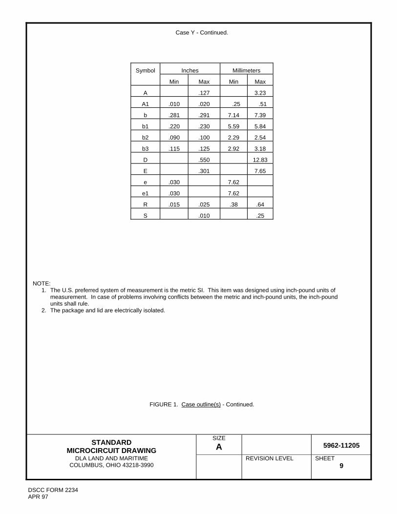
STANDARD MICROCIRCUIT DRAWING
SIZE A
5962-11205
DLA LAND AND MARITIME COLUMBUS, OHIO 43218-3990
REVISION LEVEL
SHEET 9
DSCC FORM 2234 APR 97
Case Y - Continued.
Symbol Inches Millimeters
Min Max Min Max
A .127 3.23
A1 .010 .020 .25 .51
b .281 .291 7.14 7.39
b1 .220 .230 5.59 5.84
b2 .090 .100 2.29 2.54
b3 .115 .125 2.92 3.18
D .550 12.83
E .301 7.65
e .030 7.62
e1 .030 7.62
R .015 .025 .38 .64
S .010 .25
NOTE: 1. The U.S. preferred system of measurement is the metric SI. This item was designed using inch-pound units of measurement. In case of problems involving conflicts between the metric and inch-pound units, the inch-pound units shall rule. 2. The package and lid are electrically isolated.
FIGURE 1. Case outline(s) - Continued.

STANDARD MICROCIRCUIT DRAWING
SIZE A
5962-11205
DLA LAND AND MARITIME COLUMBUS, OHIO 43218-3990
REVISION LEVEL
SHEET 10
DSCC FORM 2234 APR 97
Device types 01 02 Case outlines X Y
Terminal number Terminal symbol 1 2 3 4 5
VOUT RSET VIN ---
VIN
VSENSE RSET
VCONTROL
VOUT
FIGURE 2. Terminal connections.
FIGURE 3. Block diagram.

STANDARD MICROCIRCUIT DRAWING
SIZE A
5962-11205
DLA LAND AND MARITIME COLUMBUS, OHIO 43218-3990
REVISION LEVEL
SHEET 11
DSCC FORM 2234 APR 97
FIGURE 3. Block diagram - Continued..

STANDARD MICROCIRCUIT DRAWING
SIZE A
5962-11205
DLA LAND AND MARITIME COLUMBUS, OHIO 43218-3990
REVISION LEVEL
SHEET 12
DSCC FORM 2234 APR 97
Case
Temperature (C)
Maximum power
dissipation (Watts)
0 30.0 10 28.0 20 26.0 30 24.0 40 22.0 50 20.0 60 18.0 70 16.0 80 14.0 90 12.0
100 10.0 110 8.0 120 6.0 130 4.0 140 2.0 150 0.0
FIGURE 4. Maximum power dissipation verses case temperature chart.

STANDARD MICROCIRCUIT DRAWING
SIZE A
5962-11205
DLA LAND AND MARITIME COLUMBUS, OHIO 43218-3990
REVISION LEVEL
SHEET 13
DSCC FORM 2234 APR 97
TABLE II. Electrical test requirements.
MIL-PRF-38534 test requirements Subgroups
(in accordance with MIL-PRF-38534, group A
test table) Interim electrical parameters
---
Final electrical parameters
1*,2,3
Group A test requirements
1,2,3
Group C end-point electrical parameters
1,2,3
End-point electrical parameters for Radiation Hardness Assurance (RHA) devices
1
* PDA applies to subgroup 1.
4. VERIFICATION
4.1 Sampling and inspection. Sampling and inspection procedures shall be in accordance with MIL-PRF-38534 or as modified
in the device manufacturer's Quality Management (QM) plan. The modification in the QM plan shall not affect the form, fit, or function as described herein. 4.2 Screening. Screening shall be in accordance with MIL-PRF-38534. The following additional criteria shall apply:
a. Burn-in test, method 1015 of MIL-STD-883.
(1) Test condition A, B, C, or D. The test circuit shall be maintained by the manufacturer under document revision level control and shall be made available to either DLA Land and Maritime -VA or the acquiring activity upon request. Also, the test circuit shall specify the inputs, outputs, biases, and power dissipation, as applicable, in accordance with the intent specified in method 1015 of MIL-STD-883.
(2) TA as specified in accordance with table I of method 1015 of MIL-STD-883.
b. Interim and final electrical test parameters shall be as specified in table II herein, except interim electrical parameter tests
prior to burn-in are optional at the discretion of the manufacturer.
4.3 Conformance and periodic inspections. Conformance inspection (CI) and periodic inspection (PI) shall be in accordance with MIL-PRF-38534 and as specified herein.
4.3.1 Group A inspection (CI). Group A inspection shall be in accordance with MIL-PRF-38534 and as follows:
a. Tests shall be as specified in table II herein.
b. Subgroups 4, 5, 6, 7, 8A, 8B, 9, 10, and 11 shall be omitted.
4.3.2 Group B inspection (PI). Group B inspection shall be in accordance with MIL-PRF-38534.

STANDARD MICROCIRCUIT DRAWING
SIZE A
5962-11205
DLA LAND AND MARITIME COLUMBUS, OHIO 43218-3990
REVISION LEVEL
SHEET 14
DSCC FORM 2234 APR 97
4.3.3 Group C inspection (PI). Group C inspection shall be in accordance with MIL-PRF-38534 and as follows:
a. End-point electrical parameters shall be as specified in table II herein.
b. Steady-state life test, method 1005 of MIL-STD-883.
(1) Test condition A, B, C, or D. The test circuit shall be maintained by the manufacturer under document revision level control and shall be made available to either DLA Land and Maritime -VA or the acquiring activity upon request. Also, the test circuit shall specify the inputs, outputs, biases, and power dissipation, as applicable, in accordance with the intent specified in method 1005 of MIL-STD-883.
(2) TA as specified in accordance with table I of method 1005 of MIL-STD-883.
(3) Test duration: 1,000 hours, except as permitted by method 1005 of MIL-STD-883.
4.3.4 Group D inspection (PI). Group D inspection shall be in accordance with MIL-PRF-38534.
4.3.5 Radiation Hardness Assurance (RHA) inspection. RHA qualification is required for those devices with the RHA
designator as specified herein. End-point electrical parameters for radiation hardness assurance (RHA) devices shall be specified in table II. Radiation testing will be in accordance with the qualifying activity (DLA Land and Maritime -VQ) approved plan and with MIL-PRF-38534, Appendix G.
4.3.5.1 Total dose irradiation testing. Total dose irradiation testing shall be in accordance with MIL-STD-883 method 1019,
condition A and as specified herein. Sample testing in accordance with table I shall be performed on a representative device type (similar device) at initial qualification and after any design or process changes which may affect the RHA response. Sample size is a minimum of 8 devices (4 biased and 4 not biased). This sample testing is repeated for each new combination for wafers of active elements on the most complex device.
5. PACKAGING
5.1 Packaging requirements. The requirements for packaging shall be in accordance with MIL-PRF-38534.
6. NOTES
6.1 Intended use. Microcircuits conforming to this drawing are intended for use for Government microcircuit applications
(original equipment), design applications, and logistics purposes. 6.2 Replaceability. Microcircuits covered by this drawing will replace the same generic device covered by a contractor- prepared specification or drawing.
6.3 Configuration control of SMD's. All proposed changes to existing SMD's will be coordinated as specified in MIL-PRF-
38534. 6.4 Record of users. Military and industrial users shall inform DLA Land and Maritime when a system application requires
configuration control and the applicable SMD. DLA Land and Maritime will maintain a record of users and this list will be used for coordination and distribution of changes to the drawings. Users of drawings covering microelectronic devices (FSC 5962) should contact DLA Land and Maritime -VA, telephone (614) 692-0544.
6.5 Comments. Comments on this drawing should be directed to DLA Land and Maritime -VA, Columbus, Ohio 43218-3990, or
telephone (614) 692-1081.
6.6 Sources of supply. Sources of supply are listed in MIL-HDBK-103 and QML-38534. The vendors listed in MIL-HDBK-103 and QML-38534 have submitted a certificate of compliance (see 3.7 herein) to DLA Land and Maritime -VA and have agreed to this drawing.

STANDARD MICROCIRCUIT DRAWING BULLETIN DATE: Approved sources of supply for SMD 5962-11205 are listed below for immediate acquisition information only and shall be added to MIL-HDBK-103 and QML-38534 during the next revisions. MIL-HDBK-103 and QML-38534 will be revised to include the addition or deletion of sources. The vendors listed below have agreed to this drawing and a certificate of compliance has been submitted to and accepted by DLA Land and Maritime -VA. This information bulletin is superseded by the next dated revisions of MIL-HDBK-103 and QML-38534. DLA Land and Maritime maintains an online database of all current sources of supply at http://www.landandmaritime.dla.mil/Programs/Smcr/.
Standard
microcircuit drawing PIN 1/
Vendor CAGE
number
Vendor similar PIN 2/
5962-1120501KXA 5962R1120501KXA 5962-1120501KXC 5962R1120501KXC
88379 88379 88379 88379
VRG8665-201-2S VRG8665-901-2S VRG8665-201-1S VRG8665-901-1S
5962-1120502KYA 5962R1120502KYA 5962-1120502KYC 5962R1120502KYC
88379 88379 88379 88379
VRG8666-201-2S VRG8666-901-2S VRG8666-201-1S VRG8666-901-1S
1/ The lead finish shown for each PIN representing
a hermetic package is the most readily available from the manufacturer listed for that part. If the desired lead finish is not listed contact the Vendor to determine its availability.
2/ Caution. Do not use this number for item acquisition. Items acquired to this number may not satisfy the performance requirements of this drawing.
.
Vendor CAGE Vendor name number and address
88379 Aeroflex Plainview Incorporated, (Aeroflex Microelectronics Solutions)
35 South Service Road Plainview, NY 11803-4193
The information contained herein is disseminated for convenience only and the Government assumes no liability whatsoever for any inaccuracies in the information bulletin.
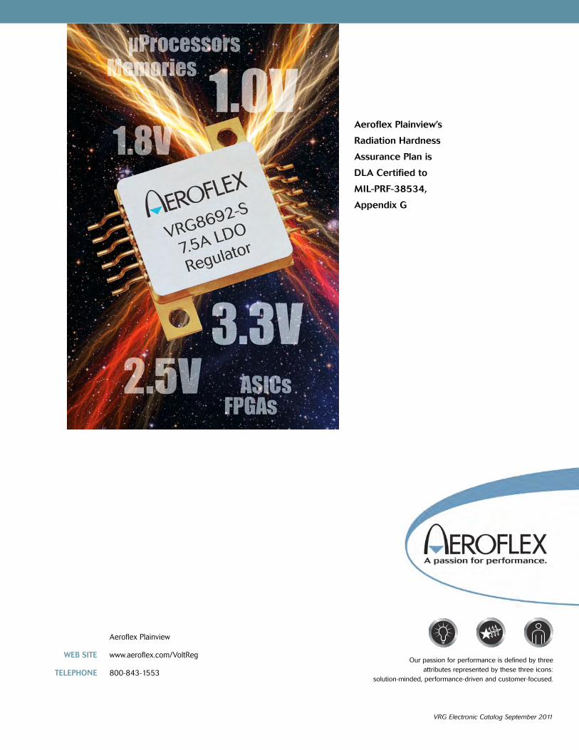
Aeroflex Plainview
WEB SITE www.aeroflex.com/VoltReg
TELEPHONE 800-843-1553
Our passion for performance is defined by three attributes represented by these three icons:
solution-minded, performance-driven and customer-focused.
VRG Electronic Catalog September 2011
Aeroflex Plainview’s
Radiation Hardness
Assurance Plan is
DLA Certified to
MIL-PRF-38534,
Appendix G