vm7000a paperless recorder communication …tw.accukloud.com/photo/article/220/file172.pdf ·...
TRANSCRIPT

VM7000A PAPERLESS RECORDER
COMMUNICATION FUNCTION OPERATION MANUAL
WXPVM70mnA0002E March, 2014(Rev.5)
Copyright © 2009-2014, Ohkura Electric Co.,Ltd. All Rights Reserved.
- i -
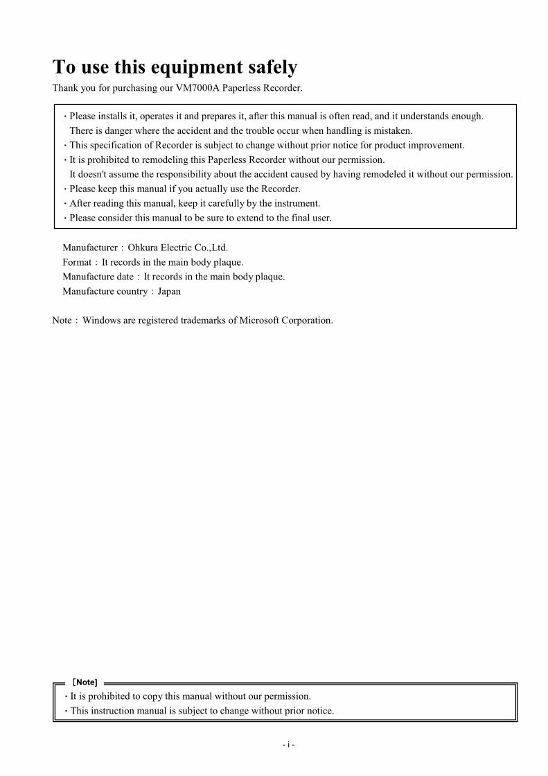
To use this equipment safely Thank you for purchasing our VM7000A Paperless Recorder.
Manufacturer:Ohkura Electric Co.,Ltd. Format:It records in the main body plaque. Manufacture date:It records in the main body plaque. Manufacture country:Japan Note:Windows are registered trademarks of Microsoft Corporation.
・Please installs it, operates it and prepares it, after this manual is often read, and it understands enough. There is danger where the accident and the trouble occur when handling is mistaken. ・This specification of Recorder is subject to change without prior notice for product improvement. ・It is prohibited to remodeling this Paperless Recorder without our permission. It doesn't assume the responsibility about the accident caused by having remodeled it without our permission. ・Please keep this manual if you actually use the Recorder. ・After reading this manual, keep it carefully by the instrument. ・Please consider this manual to be sure to extend to the final user.
・It is prohibited to copy this manual without our permission. ・This instruction manual is subject to change without prior notice.
[Note]

- ii -
The symbols below are used on this instrument for the cautioning information.
Be sure to observe the following warnings/cautions and those provided in the text in order to secure safety in handling the instrument.
WARNING ● In order to prevent electric shock; be to disconnect this instrument from the main
power source when wiring it.
● In order to prevent an electric shock; be sure to provide protective grounding prior to turning on this instrument.
● Do not cut a protective grounding conductor or disconnect protective grounding.
● Make sure that the supply voltage for this instrument conforms to the voltage of the supply source.
● Do not operate this instrument in the environment where it is exposed to a
combustible / explosive / corrosive gas or water / steam.
● Provide input and output wring after turning off the power.
Symbols used on the instrument
This shows “Caution for handling”. This symbol is used on the parts need to reference the instruction manual for saving human body and the instrument.
This shows “Protective grounding”. Be sure to provide protective grounding prior to operate this instrument.
This shows “Risk of electric shock”. This symbol is used on the parts, which has a risk of electric shock.
General
Pro tect ive Grounding
Power Source
Working Envi ronment
Input and Output W i r ing

- iii -
CAUTION
● Do not use empty terminals for other purposes such as relaying, etc.
● Please confirm the direction to the insertion of SD card. When forcibly inserting it in a wrong direction, SD card and the terminal on the main body side might be destroyed. Please mote that the damage of the equipment by the reverse-insertion becomes off the subject of amends.
● Do not replace the main unit or printed circuit boards. When this is neglected, we cannot guarantee functioning of the instrument. Contact our dealer where you purchased the instrument, or our sales representative.
[Note]
● Deliver this instruction manual to an end user. ● Prior to handling this instrument, be sure to read this manual. ● If you have any questions on this manual or find any errors or omissions in this
manual, contact our sales representative. ● After reading this manual, keep it carefully by the instrument. ● When the manual is lost or stained, contact our sales representative. ● It is prohibited to copy or reproduce this manual without our permission. ● When installing this instrument, put on a protective gear such as safety shoes,
helmet, etc. for your safety. ● Do not put your foot on the installed instrument or get on it, because it is dangerous. ● Only our serviceman or persons authorized are allowed to remove and take the inner
module, the main unit and printed circuit boards apart. ● Use dry cloth to clean the surface of this instrument. ● Do not use any organic solvent. ● Cleaning the instrument after turning off the power. ● This instruction manual is subject to change without prior notice.
Inside of Ins trument
Input and Output Wiring
Reverse-insertion attention
Ins truct ion Manual
Ins ta l lat ion
Maintenance
Cleaning
Revis ions

- iv -
<CONTENTS>
1. INTRODUCTION .......................................................................................... 1-1
1.1 About the communication protocol ........................................................................................................ 1-1 1.2 Outline of Ethernet communication function.......................................................................................... 1-1 1.3 RS-485(option) ...................................................................................................................................... 1-1 1.4 Preparation ........................................................................................................................................... 1-1 1.5 Modbus RTU protocol ........................................................................................................................... 1-2 1.6 Modbus TCP protocol ........................................................................................................................... 1-2 1.7 Addition of new items and map version ................................................................................................ 1-2
2. READ AND WRITE OF DATA ..................................................................... 2-1 2.1 Communication Protocol (Modbus TCP or Modbus RTU)..................................................................... 2-1 2.2 Function code ....................................................................................................................................... 2-1 2.3 Error Response ..................................................................................................................................... 2-2 2.4 Reading of input register area ............................................................................................................... 2-3 2.5 Read and write of holding register area ................................................................................................ 2-16 2.6 Other setting range ............................................................................................................................... 2-33

1-1
1. INTRODUCTION
1.1 About the communication protocol This equipment is equipped with the Modbus protocol. The Modbus protocol has been described to protocol specifications (PI-MBUS-300 Rev.J) by the communication protocol that Modicon Inc.(AEG Schneider Automation International S.A.S) developed for PLC. Please see this specifications for the specification of the Modbus protocol. In this manual, the function code and the content of data of the Modbus protocol that can be chiefly used with this equipment have been described.
1.2 Outline of Ethernet communication function The following functions can be used according to the Ethernet communication. (1) FTP server The Recorded data preserved on the SD card installed in the recorder can be read with attached Data Viewer software. (2) Web server The status of measurements, state of the warning generation, and record start/stop condition etc. of the recorder can be easily confirmed by a browser of the personal computer. (A browser must use Internet Explorer. ) (3) Modbus TCP function It communicates with equipment such as the Modbus TCP function personal computers and PLC, and measurements and various data can be sent and received. (4) SNTP clients The time data is regularly received from the time server by using the network, and the time of the recorder is corrected.
1.3 RS-485(option) It is possible to communicate by RS-485 (option). The protocol becomes Modbus RTU.
1.4 Preparation Push the MENU button of the main body of the recorder. Next, touch in order of the System and Comm. Various set menus concerning the communication are displayed. Please set it variously referring to the manual of the main body of the recorder. (Refer item 8.6 of Paperless Recorder Manual for Comm.)
1-2
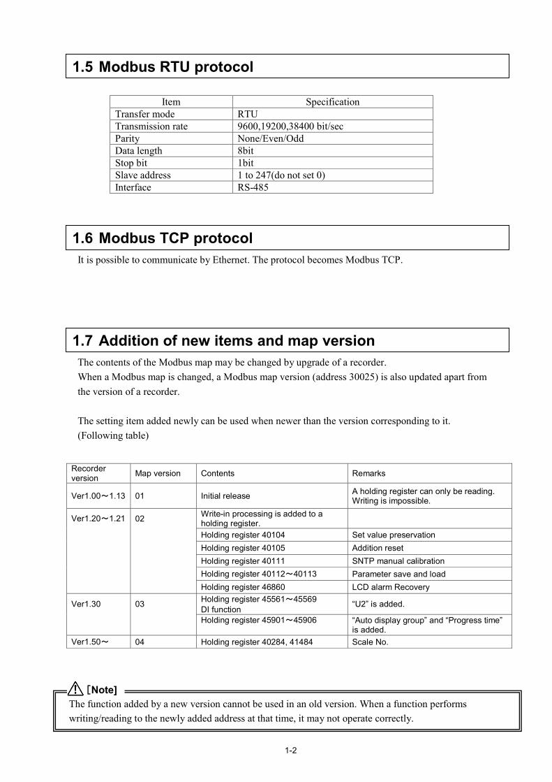
1.5 Modbus RTU protocol
Item Specification Transfer mode RTU Transmission rate 9600,19200,38400 bit/sec Parity None/Even/Odd Data length 8bit Stop bit 1bit Slave address 1 to 247(do not set 0) Interface RS-485
1.6 Modbus TCP protocol It is possible to communicate by Ethernet. The protocol becomes Modbus TCP.
1.7 Addition of new items and map version The contents of the Modbus map may be changed by upgrade of a recorder. When a Modbus map is changed, a Modbus map version (address 30025) is also updated apart from the version of a recorder. The setting item added newly can be used when newer than the version corresponding to it. (Following table)
Recorder version Map version Contents Remarks
Ver1.00~1.13 01 Initial release A holding register can only be reading. Writing is impossible.
Ver1.20~1.21 02 Write-in processing is added to a holding register.
Holding register 40104 Set value preservation Holding register 40105 Addition reset Holding register 40111 SNTP manual calibration Holding register 40112~40113 Parameter save and load Holding register 46860 LCD alarm Recovery
Ver1.30 03 Holding register 45561~45569 DI function “U2” is added.
Holding register 45901~45906
“Auto display group” and “Progress time” is added.
Ver1.50~ 04 Holding register 40284, 41484 Scale No.
The function added by a new version cannot be used in an old version. When a function performs writing/reading to the newly added address at that time, it may not operate correctly.
[Note]

2-1
2. READ AND WRITE OF DATA 2.1 Communication Protocol (Modbus TCP or Modbus RTU) This product supports two types of Modbus protocols: Modbus TCP protocol that works on Ethernet and
Modbus RTU that works on RS-485.
Shown below are the differences between these two protocols. The function code and data sections are the
same, but there are differences in the header and error check sections.
Modbus TCP MBAP header
(7 bytes) Function code
(1 byte) Data
(variable)
MBAP header
Transfer ID (2 bytes)
Protocol ID (2 bytes)
Data length (2 bytes)
Slave address (1 byte)
High-order Low-order High-order Low-order High-order Low-order
[MBAP header]
Function
Transfer ID The ID for data recognition. The same ID will return in every response.
Protocol ID Fixed to 0.
Data length The sum of the lengths of the slave address, function code, and data sections.
Slave address Indicates the slave address. (It is used, for example, to convert between Modbus TCP and Modbus RTU.)
Modbus RTU Slave address
(1 byte) Function code
(1 byte) Data
(variable) CRC
(2 bytes)
2.2 Function code The function code that can be used with this equipment is as follows.
Code Function Maximum data length Modbus original function (reference)
03H Reading of the setting data 123 words Holding register content reading
04H Reading of content of input register 123 words Reading of content of input register
06H Writing of data 1 words Holding register content writing

2-2
2.3 Error Response In accordance with the communication protocol for the pertinent function code, if an error occurs during
command transmission, an error response is returned in the fixed format described in this section.
■ Example of slave response (function code = 06H, command error = 10H)
Component Data length Data TCP RTU MBAP header (only for Modbus TCP) 7 - - Slave address (only for Modbus RTU) - 1 - Function code + 80H 1 1 86H Error code 1 1 10H Error check (only for Modbus RTU) - 2 CRC Total number of bytes 9 5 -
● Error codes and their occurrence conditions Error code Description Occurrence condition(s)
01H Invalid function code An unsupported function code is specified.
02H Invalid register address The relative address range exceeds "9999."
03H Invalid number of registers
- The length of the accessed data is "0" or the sum of the relative address and data length exceeds the limit. - It is assumed that two or more function codes, each executable for one area, are involved. - Data longer than 2 words is specified for a one-time write command. - The data length exceeds 123 words.
04H Device error The received data is shorter than the predefined data length. 10H Command error An attempt at a write over an area exceeding the writable range.

2-3
2.4 Reading of input register area It is an area only for reading. The starting address of the read data (relative address) and the number of data (Every one word = two bytes) are specified. Function code: 04H
■ Example of transmitting master(starting address=0032H, data length=2words)
Component Data length Data TCP RTU MBAP header (only for Modbus TCP) 7 - - Slave address - 1 - Function code 1 1 04H
Data
Relative start address (high-order) 1 1 00H Relative start address (low-order) 1 1 32H Read data count (high-order) 1 1 00H Read data count (low-order) 1 1 02H
Error check - 2 CRC (16 bits) Total number of bytes 12 8
■Example of slave's responding (starting address=0032H, data length =2words)
Component Data length Data TCP RTU MBAP header (only for Modbus TCP) 7 - - Slave address - 1 - Function code 1 1 04H
Data
Number of data bytes 1 1 04H Data 1 (high-order) 1 1 00H Data 1 (low-order) 1 1 09H Data 2 (high-order) 1 1 00H Data 2 (low-order) 1 1 0AH
Error check - 2 CRC (16 bits) Total number of bytes 13 9

2-4
【Input register area map】Function code: 04H
Address Relative address (HEX)
Item Array Content Remarks
30001 0 Production number 1 ASCII 30002 1 Production number 2 ASCII 30003 2 Production number 3 ASCII 30004 3 Production number 4 ASCII 30005 4 Production number 5 ASCII 30006 5 Production number 6 ASCII 30007 6 Production number 7 ASCII 30008 7 Production number 8 ASCII 30009 8 Software version 1 ASCII 30010 9 Software version 2 ASCII 30011 A Software version 3 ASCII 30012 B Software version 4 ASCII 30013 C Software version 5 ASCII 30014 D Software version 6 ASCII 30015 E Software version 7 ASCII 30016 F Software version 8 ASCII 30017 10 Software version 9 ASCII 30018 11 Software version 10 ASCII 30019 12 Software version 11 ASCII 30020 13 Software version 12 ASCII 30021 14 Software version 13 ASCII 30022 15 Software version 14 ASCII 30023 16 Software version 15 ASCII 30024 17 Software version 16 ASCII 30025 18 Modbus Map version 1 Binary ※ Refer item 1.7 30026 19 Reserve 1 30027 1A Reserve 2 30028 1B Reserve 3 30029 1C Reserve 4 30030 1D Reserve 5 30031 1E Reserve 6 30032 1F Reserve 7 30033 20 Reserve 8 30034 21 Reserve 9 30035 22 Reserve 10 30036 23 MAC address 1 30037 24 MAC address 2 30038 25 MAC address 3 30039 26 Reserve 30040 27 Reserve 30041 28 Reserve 30042 29 Reserve 30043 2A Reserve 30044 2B Reserve 30045 2C Reserve 30046 2D Reserve 30047 2E Reserve 30048 2F Reserve 30049 30 Reserve

2-5
Address Relative address (HEX)
Item Array Content Remarks
30050 31 Reserve 30051 32 Year 0~99 30052 33 Month 1~12 30053 34 Day 1~31 30054 35 Hour 0~24 30055 36 Minute 0~59 30056 37 Second 0~59
30057 38 State of internal memory remainder 0~1000
Unit: % (one digit after the decimal point)
30058 39 SD card connection 0~1 0:Unconnection 1: Connection
30059 3A SD card remainder capacity 0~1000 Unit: % (one digit after the decimal point)
30060 3B State of record 0~1 0:Record stop 1: Record start 30061 3C State of subrecord 0~1 0:Record stop 1: Record start 30062 3D State of battery 0~1 0:Normality 1: Abnormality 30063 3E Reserve 30064 3F Reserve 30065 40 Reserve 30066 41 Reserve 30067 42 Reserve 30068 43 Reserve 30069 44 Reserve 30070 45 Reserve 30071 46 Reserve 30072 47 Reserve 30073 48 Reserve 30074 49 Reserve 30075 4A Reserve 30076 4B Reserve 30077 4C Reserve 30078 4D Reserve 30079 4E Reserve 30080 4F Reserve 30081 50 Reserve 30082 51 Reserve 30083 52 Reserve 30084 53 Reserve 30085 54 Reserve 30086 55 Reserve 30087 56 Reserve 30088 57 Reserve 30089 58 Reserve 30090 59 Reserve 30091 5A Reserve 30092 5B Reserve 30093 5C Reserve 30094 5D Reserve 30095 5E Reserve 30096 5F Reserve 30097 60 Reserve 30098 61 Reserve 30099 62 Reserve

2-6
Address Relative address (HEX)
Item Array Content Remarks
30100 63 Reserve 30101 64 Measurements CH01 -32000~32000 30102 65 Measurements CH02 -32000~32000 30103 66 Measurements CH03 -32000~32000 30104 67 Measurements CH04 -32000~32000 30105 68 Measurements CH05 -32000~32000 30106 69 Measurements CH06 -32000~32000 30107 6A Measurements CH07 -32000~32000 30108 6B Measurements CH08 -32000~32000 30109 6C Measurements CH09 -32000~32000 30110 6D Measurements CH10 -32000~32000 30111 6E Measurements CH11 -32000~32000 30112 6F Measurements CH12 -32000~32000 30113 70 Measurements CH13 -32000~32000 30114 71 Measurements CH14 -32000~32000 30115 72 Measurements CH15 -32000~32000 30116 73 Measurements CH16 -32000~32000 30117 74 Measurements CH17 -32000~32000 30118 75 Measurements CH18 -32000~32000 30119 76 Measurements CH19 -32000~32000 30120 77 Measurements CH20 -32000~32000 30121 78 Measurements CH21 -32000~32000 30122 79 Measurements CH22 -32000~32000 30123 7A Measurements CH23 -32000~32000 30124 7B Measurements CH24 -32000~32000 30125 7C Measurements CH25 -32000~32000 30126 7D Measurements CH26 -32000~32000 30127 7E Measurements CH27 -32000~32000 30128 7F Measurements CH28 -32000~32000 30129 80 Measurements CH29 -32000~32000 30130 81 Measurements CH30 -32000~32000 30131 82 Measurements CH31 -32000~32000 30132 83 Measurements CH32 -32000~32000 30133 84 Measurements CH33 -32000~32000 30134 85 Measurements CH34 -32000~32000 30135 86 Measurements CH35 -32000~32000 30136 87 Measurements CH36 -32000~32000 30137 88 Measurements CH37 -32000~32000 30138 89 Measurements CH38 -32000~32000 30139 8A Measurements CH39 -32000~32000 30140 8B Measurements CH40 -32000~32000 30141 8C Measurements CH41 -32000~32000 30142 8D Measurements CH42 -32000~32000 30143 8E Measurements CH43 -32000~32000 30144 8F Measurements CH44 -32000~32000 30145 90 Measurements CH45 -32000~32000 30146 91 Measurements CH46 -32000~32000 30147 92 Measurements CH47 -32000~32000 30148 93 Measurements CH48 -32000~32000 30149 94 Reserve 30150 95 Reserve

2-7
Address Relative address (HEX)
Item Array Content Remarks
30151 96 Reserve 30152 97 Reserve 30153 98 Reserve 30154 99 Reserve 30155 9A Reserve 30156 9B Reserve 30157 9C Reserve 30158 9D Reserve 30159 9E Reserve 30160 9F Reserve 30161 A0 Reserve 30162 A1 Reserve 30163 A2 Reserve 30164 A3 Reserve 30165 A4 Reserve 30166 A5 Reserve 30167 A6 Reserve 30168 A7 Reserve 30169 A8 Reserve 30170 A9 Reserve 30171 AA Reserve 30172 AB Reserve 30173 AC Reserve 30174 AD Reserve 30175 AE Reserve 30176 AF Reserve 30177 B0 Reserve 30178 B1 Reserve 30179 B2 Reserve 30180 B3 Reserve 30181 B4 Reserve 30182 B5 Reserve 30183 B6 Reserve 30184 B7 Reserve 30185 B8 Reserve 30186 B9 Reserve 30187 BA Reserve 30188 BB Reserve 30189 BC Reserve 30190 BD Reserve 30191 BE Reserve 30192 BF Reserve 30193 C0 Reserve 30194 C1 Reserve 30195 C2 Reserve 30196 C3 Reserve 30197 C4 Reserve 30198 C5 Reserve 30199 C6 Reserve 30200 C7 Reserve

2-8
Address Relative address (HEX)
Item Array Content Remarks
30201 C8 State of channel CH01 Bit watch (Details are the following) 30202 C9 State of channel CH02 00bit: Alarm1 1= generation 0= release 30203 CA State of channel CH03 01bit: Alarm1 1= generation 0= release 30204 CB State of channel CH04 02bit: Alarm1 1= generation 0= release 30205 CC State of channel CH05 03bit: Alarm1 1= generation 0= release 30206 CD State of channel CH06 08bit:H over 1= generation 0= release 30207 CE State of channel CH07 09bit:L over 1= generation 0= release 30208 CF State of channel CH08 10bit:Burnout 1= generation 0= release 30209 D0 State of channel CH09 11bit:Fault 1= generation 0= release 30210 D1 State of channel CH10 12bit:AD abnormal 1= generation 0= release 30211 D2 State of channel CH11 30212 D3 State of channel CH12 30213 D4 State of channel CH13 30214 D5 State of channel CH14 30215 D6 State of channel CH15 30216 D7 State of channel CH16 30217 D8 State of channel CH17 30218 D9 State of channel CH18 30219 DA State of channel CH19 30220 DB State of channel CH20 30221 DC State of channel CH21 30222 DD State of channel CH22 30223 DE State of channel CH23 30224 DF State of channel CH24 30225 E0 State of channel CH25 30226 E1 State of channel CH26 30227 E2 State of channel CH27 30228 E3 State of channel CH28 30229 E4 State of channel CH29 30230 E5 State of channel CH30 30231 E6 State of channel CH31 30232 E7 State of channel CH32 30233 E8 State of channel CH33 30234 E9 State of channel CH34 30235 EA State of channel CH35 30236 EB State of channel CH36 30237 EC State of channel CH37 30238 ED State of channel CH38 30239 EE State of channel CH39 30240 EF State of channel CH40 30241 F0 State of channel CH41 30242 F1 State of channel CH42 30243 F2 State of channel CH43 30244 F3 State of channel CH44 30245 F4 State of channel CH45 30246 F5 State of channel CH46 30247 F6 State of channel CH47 30248 F7 State of channel CH48 30249 F8 Reserve 30250 F9 Reserve 30251 FA Reserve
2-9
Address Relative address (HEX)
Item Array Content Remarks
30252 FB Reserve 30253 FC Reserve 30254 FD Reserve 30255 FE Reserve 30256 FF Reserve 30257 100 Reserve 30258 101 Reserve 30259 102 Reserve 30260 103 Reserve 30261 104 Reserve 30262 105 Reserve 30263 106 Reserve 30264 107 Reserve 30265 108 Reserve 30266 109 Reserve 30267 10A Reserve 30268 10B Reserve 30269 10C Reserve 30270 10D Reserve 30271 10E Reserve 30272 10F Reserve 30273 110 Reserve 30274 111 Reserve 30275 112 Reserve 30276 113 Reserve 30277 114 Reserve 30278 115 Reserve 30279 116 Reserve 30280 117 Reserve 30281 118 Reserve 30282 119 Reserve 30283 11A Reserve 30284 11B Reserve 30285 11C Reserve 30286 11D Reserve 30287 11E Reserve 30288 11F Reserve 30289 120 Reserve 30290 121 Reserve 30291 122 Reserve 30292 123 Reserve 30293 124 Reserve 30294 125 Reserve 30295 126 Reserve 30296 127 Reserve 30297 128 Reserve 30298 129 Reserve 30299 12A Reserve 30300 12B Reserve

2-10
Address Relative address (HEX)
Item Array Content Remarks
30301 12C Decimal point position CH01 0~4 30302 12D Decimal point position CH02 0~4 30303 12E Decimal point position CH03 0~4 30304 12F Decimal point position CH04 0~4 30305 130 Decimal point position CH05 0~4 30306 131 Decimal point position CH06 0~4
30307 132 Decimal point position CH07 0~4 30308 133 Decimal point position CH08 0~4 30309 134 Decimal point position CH09 0~4 30310 135 Decimal point position CH10 0~4 30311 136 Decimal point position CH11 0~4 30312 137 Decimal point position CH12 0~4 30313 138 Decimal point position CH13 0~4 30314 139 Decimal point position CH14 0~4 30315 13A Decimal point position CH15 0~4 30316 13B Decimal point position CH16 0~4 30317 13C Decimal point position CH17 0~4 30318 13D Decimal point position CH18 0~4 30319 13E Decimal point position CH19 0~4 30320 13F Decimal point position CH20 0~4 30321 140 Decimal point position CH21 0~4 30322 141 Decimal point position CH22 0~4 30323 142 Decimal point position CH23 0~4 30324 143 Decimal point position CH24 0~4 30325 144 Decimal point position CH25 0~4 30326 145 Decimal point position CH26 0~4 30327 146 Decimal point position CH27 0~4 30328 147 Decimal point position CH28 0~4 30329 148 Decimal point position CH29 0~4 30330 149 Decimal point position CH30 0~4 30331 14A Decimal point position CH31 0~4 30332 14B Decimal point position CH32 0~4 30333 14C Decimal point position CH33 0~4 30334 14D Decimal point position CH34 0~4 30335 14E Decimal point position CH35 0~4 30336 14F Decimal point position CH36 0~4 30337 150 Decimal point position CH37 0~4 30338 151 Decimal point position CH38 0~4 30339 152 Decimal point position CH39 0~4 30340 153 Decimal point position CH40 0~4 30341 154 Decimal point position CH41 0~4 30342 155 Decimal point position CH42 0~4 30343 156 Decimal point position CH43 0~4 30344 157 Decimal point position CH44 0~4 30345 158 Decimal point position CH45 0~4 30346 159 Decimal point position CH46 0~4 30347 15A Decimal point position CH47 0~4 30348 15B Decimal point position CH48 0~4 30349 15C Reserve 30350 15D Reserve
30351 15E Reserve

2-11
Address Relative address (HEX)
Item Array Content Remarks
30352 15F Reserve 30353 160 Reserve 30354 161 Reserve 30355 162 Reserve 30356 163 Reserve 30357 164 Reserve 30358 165 Reserve 30359 166 Reserve 30360 167 Reserve 30361 168 Reserve 30362 169 Reserve 30363 16A Reserve 30364 16B Reserve 30365 16C Reserve 30366 16D Reserve 30367 16E Reserve 30368 16F Reserve 30369 170 Reserve 30370 171 Reserve 30371 172 Reserve 30372 173 Reserve 30373 174 Reserve 30374 175 Reserve 30375 176 Reserve 30376 177 Reserve 30377 178 Reserve 30378 179 Reserve 30379 17A Reserve 30380 17B Reserve 30381 17C Reserve 30382 17D Reserve 30383 17E Reserve 30384 17F Reserve 30385 180 Reserve 30386 181 Reserve 30387 182 Reserve 30388 183 Reserve 30389 184 Reserve 30390 185 Reserve 30391 186 Reserve 30392 187 Reserve 30393 188 Reserve 30394 189 Reserve 30395 18A Reserve 30396 18B Reserve 30397 18C Reserve 30398 18D Reserve 30399 18E Reserve 30400 18F Reserve 30401 190 Unit (1/4) CH01 30402 191 Unit (2/4) CH01
2-12
Address Relative address (HEX)
Item Array Content Remarks
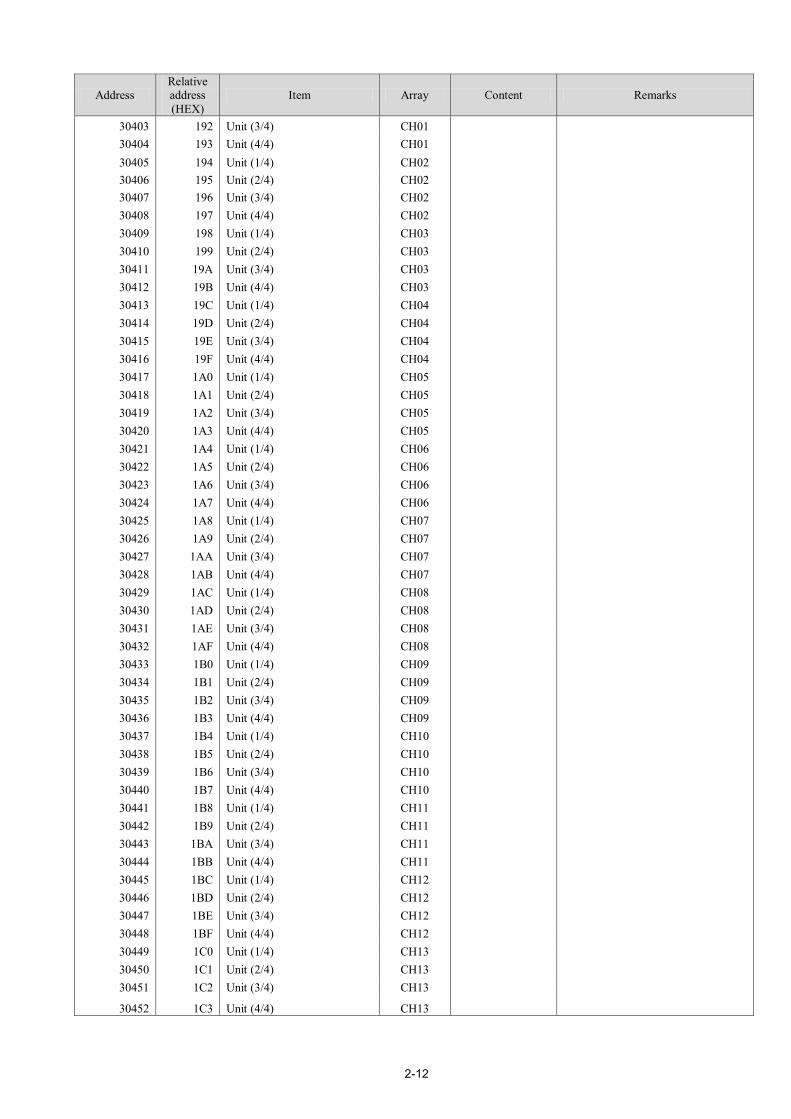
30403 192 Unit (3/4) CH01 30404 193 Unit (4/4) CH01 30405 194 Unit (1/4) CH02 30406 195 Unit (2/4) CH02 30407 196 Unit (3/4) CH02 30408 197 Unit (4/4) CH02 30409 198 Unit (1/4) CH03 30410 199 Unit (2/4) CH03 30411 19A Unit (3/4) CH03 30412 19B Unit (4/4) CH03 30413 19C Unit (1/4) CH04 30414 19D Unit (2/4) CH04 30415 19E Unit (3/4) CH04 30416 19F Unit (4/4) CH04 30417 1A0 Unit (1/4) CH05 30418 1A1 Unit (2/4) CH05 30419 1A2 Unit (3/4) CH05 30420 1A3 Unit (4/4) CH05 30421 1A4 Unit (1/4) CH06 30422 1A5 Unit (2/4) CH06 30423 1A6 Unit (3/4) CH06 30424 1A7 Unit (4/4) CH06 30425 1A8 Unit (1/4) CH07 30426 1A9 Unit (2/4) CH07 30427 1AA Unit (3/4) CH07 30428 1AB Unit (4/4) CH07 30429 1AC Unit (1/4) CH08 30430 1AD Unit (2/4) CH08 30431 1AE Unit (3/4) CH08 30432 1AF Unit (4/4) CH08 30433 1B0 Unit (1/4) CH09 30434 1B1 Unit (2/4) CH09 30435 1B2 Unit (3/4) CH09 30436 1B3 Unit (4/4) CH09 30437 1B4 Unit (1/4) CH10 30438 1B5 Unit (2/4) CH10 30439 1B6 Unit (3/4) CH10 30440 1B7 Unit (4/4) CH10 30441 1B8 Unit (1/4) CH11 30442 1B9 Unit (2/4) CH11 30443 1BA Unit (3/4) CH11 30444 1BB Unit (4/4) CH11 30445 1BC Unit (1/4) CH12 30446 1BD Unit (2/4) CH12 30447 1BE Unit (3/4) CH12 30448 1BF Unit (4/4) CH12 30449 1C0 Unit (1/4) CH13 30450 1C1 Unit (2/4) CH13 30451 1C2 Unit (3/4) CH13
30452 1C3 Unit (4/4) CH13

2-13
Address Relative address (HEX)
Item Array Content Remarks
30453 1C4 Unit (1/4) CH14 30454 1C5 Unit (2/4) CH14 30455 1C6 Unit (3/4) CH14 30456 1C7 Unit (4/4) CH14 30457 1C8 Unit (1/4) CH15 30458 1C9 Unit (2/4) CH15 30459 1CA Unit (3/4) CH15 30460 1CB Unit (4/4) CH15 30461 1CC Unit (1/4) CH16 30462 1CD Unit (2/4) CH16 30463 1CE Unit (3/4) CH16 30464 1CF Unit (4/4) CH16 30465 1D0 Unit (1/4) CH17 30466 1D1 Unit (2/4) CH17 30467 1D2 Unit (3/4) CH17 30468 1D3 Unit (4/4) CH17 30469 1D4 Unit (1/4) CH18 30470 1D5 Unit (2/4) CH18 30471 1D6 Unit (3/4) CH18 30472 1D7 Unit (4/4) CH18 30473 1D8 Unit (1/4) CH19 30474 1D9 Unit (2/4) CH19 30475 1DA Unit (3/4) CH19 30476 1DB Unit (4/4) CH19 30477 1DC Unit (1/4) CH20 30478 1DD Unit (2/4) CH20 30479 1DE Unit (3/4) CH20 30480 1DF Unit (4/4) CH20 30481 1E0 Unit (1/4) CH21 30482 1E1 Unit (2/4) CH21 30483 1E2 Unit(3/4) CH21 30484 1E3 Unit(4/4) CH21 30485 1E4 Unit(1/4) CH22 30486 1E5 Unit(2/4) CH22 30487 1E6 Unit(3/4) CH22 30488 1E7 Unit(4/4) CH22 30489 1E8 Unit(1/4) CH23 30490 1E9 Unit(2/4) CH23 30491 1EA Unit(3/4) CH23 30492 1EB Unit(4/4) CH23 30493 1EC Unit(1/4) CH24 30494 1ED Unit(2/4) CH24 30495 1EE Unit(3/4) CH24 30496 1EF Unit(4/4) CH24 30497 1F0 Unit(1/4) CH25 30498 1F1 Unit(2/4) CH25 30499 1F2 Unit(3/4) CH25 30500 1F3 Unit(4/4) CH25 30501 1F4 Unit(1/4) CH26
30502 1F5 Unit(2/4) CH26

2-14
Address Relative address (HEX)
Item Array Content Remarks
30503 1F6 Unit(3/4) CH26 30504 1F7 Unit(4/4) CH26 30505 1F8 Unit(1/4) CH27 30506 1F9 Unit(2/4) CH27 30507 1FA Unit(3/4) CH27 30508 1FB Unit(4/4) CH27 30509 1FC Unit(1/4) CH28 30510 1FD Unit(2/4) CH28 30511 1FE Unit(3/4) CH28 30512 1FF Unit(4/4) CH28 30513 200 Unit(1/4) CH29 30514 201 Unit(2/4) CH29 30515 202 Unit(3/4) CH29 30516 203 Unit(4/4) CH29 30517 204 Unit(1/4) CH30 30518 205 Unit(2/4) CH30 30519 206 Unit(3/4) CH30 30520 207 Unit(4/4) CH30 30521 208 Unit(1/4) CH31 30522 209 Unit(2/4) CH31 30523 20A Unit(3/4) CH31 30524 20B Unit(4/4) CH31 30525 20C Unit(1/4) CH32 30526 20D Unit(2/4) CH32 30527 20E Unit(3/4) CH32 30528 20F Unit(4/4) CH32 30529 210 Unit(1/4) CH33 30530 211 Unit(2/4) CH33 30531 212 Unit(3/4) CH33 30532 213 Unit(4/4) CH33 30533 214 Unit(1/4) CH34 30534 215 Unit(2/4) CH34 30535 216 Unit(3/4) CH34 30536 217 Unit(4/4) CH34 30537 218 Unit(1/4) CH35 30538 219 Unit(2/4) CH35 30539 21A Unit(3/4) CH35 30540 21B Unit(4/4) CH35 30541 21C Unit(1/4) CH36 30542 21D Unit(2/4) CH36 30543 21E Unit(3/4) CH36 30544 21F Unit(4/4) CH36 30545 220 Unit(1/4) CH37 30546 221 Unit(2/4) CH37 30547 222 Unit(3/4) CH37 30548 223 Unit(4/4) CH37 30549 224 Unit(1/4) CH38 30550 225 Unit(2/4) CH38 30551 226 Unit(3/4) CH38 30552 227 Unit(4/4) CH38
2-15
Address Relative address (HEX)
Item Array Content Remarks
30553 228 Unit(1/4) CH39 30554 229 Unit(2/4) CH39 30555 22A Unit(3/4) CH39 30556 22B Unit(4/4) CH39 30557 22C Unit(1/4) CH40 30558 22D Unit(2/4) CH40 30559 22E Unit(3/4) CH40 30560 22F Unit(4/4) CH40 30561 230 Unit(1/4) CH41 30562 231 Unit(2/4) CH41 30563 232 Unit(3/4) CH41 30564 233 Unit(4/4) CH41 30565 234 Unit(1/4) CH42 30566 235 Unit(2/4) CH42 30567 236 Unit(3/4) CH42 30568 237 Unit(4/4) CH42 30569 238 Unit(1/4) CH43 30570 239 Unit(2/4) CH43 30571 23A Unit(3/4) CH43 30572 23B Unit(4/4) CH43 30573 23C Unit(1/4) CH44 30574 23D Unit(2/4) CH44 30575 23E Unit(3/4) CH44 30576 23F Unit(4/4) CH44 30577 240 Unit(1/4) CH45 30578 241 Unit(2/4) CH45 30579 242 Unit(3/4) CH45 30580 243 Unit(4/4) CH45 30581 244 Unit(1/4) CH46 30582 245 Unit(2/4) CH46 30583 246 Unit(3/4) CH46 30584 247 Unit(4/4) CH46 30585 248 Unit(1/4) CH47 30586 249 Unit(2/4) CH47 30587 24A Unit(3/4) CH47 30588 24B Unit(4/4) CH47 30589 24C Unit(1/4) CH48 30590 24D Unit(2/4) CH48 30591 24E Unit(3/4) CH48 30592 24F Unit(4/4) CH48 30593 250 Reserve ・・・ ・・・ ・・・ 39000 2327 Reserve

2-16
2.5 Read and write of holding register area It is an area for reading and writing. The starting address of the read data (relative address) and the number of data (Every one word = two bytes) are specified. Refer item 2.4 ”Setting range and special setting ” for item of “※”. Function code (Reading): 03H ■ Example of transmitting master(starting address=00C8H, data length=2words)
Component Data length Data TCP RTU MBAP header (only for Modbus TCP) 7 - - Slave address - 1 - Function code 1 1 03H
Data
Relative start address (high-order) 1 1 00H Relative start address (low-order) 1 1 C8H Read data count (high-order) 1 1 00H Read data count (low-order) 1 1 02H
Error check - 2 CRC (16 bits) Total number of bytes 12 8
■Example of slave's responding (starting address=0032H, data length =2words)
Component Data length Data TCP RTU MBAP header (only for Modbus TCP) 7 - - Slave address - 1 - Function code 1 1 03H
Data
Number of data bytes 1 1 04H Data 1 (high-order) 1 1 00H Data 1 (low-order) 1 1 05H Data 2 (high-order) 1 1 00H Data 2 (low-order) 1 1 00H
Error check - 2 CRC (16 bits) Total number of bytes 13 9

2-17
Function code (Writing): 06H ■ Example of transmitting master(starting address=00C8H, data =5)
Component Data length Data TCP RTU MBAP header (only for Modbus TCP) 7 - - Slave address - 1 - Function code 1 1 06H
Data
Relative start address (high-order) 1 1 00H Relative start address (low-order) 1 1 C8H Write data (high-order) 1 1 00H Write data (low-order) 1 1 05H
Error check - 2 CRC (16 bits) Total number of bytes 12 8
■Example of slave's responding (starting address=00C8H, data =5)
Component Data length Data TCP RTU MBAP header (only for Modbus TCP) 7 - - Slave address - 1 - Function code 1 1 06H
Data
Relative start address (high-order) 1 1 00H Relative start address (low-order) 1 1 C8H Write data (high-order) 1 1 00H Write data (low-order) 1 1 05H
Error check - 2 CRC (16 bits) Total number of bytes 12 8 8
2-18
【Holding register area map】Function code: 03H, 06H
Address Relative address (HEX)
Item Array Content Remarks
40001 0 Communication channel 1-value of input 0-01 -32000~32000
40002 1 2-value of input 0-02 -32000~32000 40003 2 3-value of input 0-03 -32000~32000 40004 3 4-value of input 0-04 -32000~32000 40005 4 5-value of input 0-05 -32000~32000 40006 5 6-value of input 0-06 -32000~32000 40007 6 7-value of input 0-07 -32000~32000 40008 7 8-value of input 0-08 -32000~32000 40009 8 9-value of input 0-09 -32000~32000 40010 9 10-value of input 0-10 -32000~32000 40011 A 11-value of input 0-11 -32000~32000 40012 B 12-value of input 0-12 -32000~32000 40013 C 13-value of input 0-13 -32000~32000 40014 D 13-value of input 0-14 -32000~32000 40015 E 15-value of input 0-15 -32000~32000 40016 F 16-value of input 0-16 -32000~32000 40017 10 17-value of input 0-17 -32000~32000 40018 11 18-value of input 0-18 -32000~32000 40019 12 19-value of input 0-19 -32000~32000 40020 13 20-value of input 0-20 -32000~32000 40021 14 21-value of input 0-21 -32000~32000 40022 15 22-value of input 0-22 -32000~32000 40023 16 23-value of input 0-23 -32000~32000 40024 17 24-value of input 0-24 -32000~32000 40025 18 25-value of input 0-25 -32000~32000 40026 19 26-value of input 0-26 -32000~32000 40027 1A 27-value of input 0-27 -32000~32000 40028 1B 28-value of input 0-28 -32000~32000 40029 1C 29-value of input 0-29 -32000~32000 40030 1D 30-value of input 0-30 -32000~32000 40031 1E 31-value of input 0-31 -32000~32000 40032 1F 32-value of input 0-32 -32000~32000 40033 20 33-value of input 0-33 -32000~32000 40034 21 34-value of input 0-34 -32000~32000 40035 22 35-value of input 0-35 -32000~32000 40036 23 36-value of input 0-36 -32000~32000
40037 24 Communication channel 1-position of decimal point 0-01 0~4
40038 25 2-position of decimal point 0-02 0~4 40039 26 3-position of decimal point 0-03 0~4 40040 27 4-position of decimal point 0-04 0~4 40041 28 5-position of decimal point 0-05 0~4 40042 29 6-position of decimal point 0-06 0~4 40043 2A 7-position of decimal point 0-07 0~4 40044 2B 8-position of decimal point 0-08 0~4 40045 2C 9-position of decimal point 0-09 0~4 40046 2D 10-position of decimal point 0-10 0~4 40047 2E 11-position of decimal point 0-11 0~4

2-19
Address Relative address (HEX)
Item Array Content Remarks
40048 2F 12-position of decimal point 0-12 0~4 40049 30 13-position of decimal point 0-13 0~4 40050 31 14-position of decimal point 0-14 0~4 40051 32 15-position of decimal point 0-15 0~4 40052 33 16-position of decimal point 0-16 0~4 40053 34 17-position of decimal point 0-17 0~4 40054 35 18-position of decimal point 0-18 0~4 40055 36 19-position of decimal point 0-19 0~4 40056 37 20-position of decimal point 0-20 0~4 40057 38 21-position of decimal point 0-21 0~4 40058 39 22-position of decimal point 0-22 0~4 40059 3A 23-position of decimal point 0-23 0~4 40060 3B 24-position of decimal point 0-24 0~4 40061 3C 25-position of decimal point 0-25 0~4 40062 3D 26-position of decimal point 0-26 0~4 40063 3E 27-position of decimal point 0-27 0~4 40064 3F 28-position of decimal point 0-28 0~4 40065 40 29-position of decimal point 0-29 0~4 40066 41 30-position of decimal point 0-30 0~4 40067 42 31-position of decimal point 0-31 0~4 40068 43 32-position of decimal point 0-32 0~4 40069 44 33-position of decimal point 0-33 0~4 40070 45 34-position of decimal point 0-34 0~4 40071 46 35-position of decimal point 0-35 0~4 40072 47 36-position of decimal point 0-36 0~4 40073 48 Reserve 40074 49 Reserve 40075 4A Reserve 40076 4B Reserve 40077 4C Reserve 40078 4D Reserve 40079 4E Reserve 40080 4F Reserve 40081 50 Reserve 40082 51 Reserve 40083 52 Reserve 40084 53 Reserve 40085 54 Reserve 40086 55 Reserve 40087 56 Reserve 40088 57 Reserve 40089 58 Reserve 40090 59 Reserve 40091 5A Reserve 40092 5B Reserve 40093 5C Reserve 40094 5D Reserve 40095 5E Reserve 40096 5F Reserve 40097 60 Reserve 40098 61 Reserve

2-20
Address Relative address (HEX)
Item Array Content Remarks
40099 62 Reserve 40100 63 Reserve
40101 64 Record start/stop AA01:start AA00:stop
Invalid except the left "DI" is selected when invalid.
40102 65 Sub record start/stop
AA01:Start AA00:Stop
Invalid except the left When assigned to the Func key.
40103 66 LCD ON/OFF AA01:ON Invalid except the left According to the recorder set.
40104 67 Set value preservation AA01:preservation Invalid except the left 40105 68 Addition reset AA01:Reset ※It supports after the map version 02. 40106 69 Reserve (Refer item 1.7) 40107 6A Reserve 40108 6B Reserve 40109 6C Reserve 40110 6D Reserve 40111 6E SNTP manual calibration AA01:Calibration ※9 Refer item 2.4 40112 6F Pram save (Recorder → SD) AA01:Save ※10 Refer item 2.4 40113 70 Pram load (SD → Recorder) AA01:Load ※11 Refer item 2.4 40114 71 Reserve ※About an address 40104, 40105, 40115 72 Reserve 40111~40113, 40116 73 Reserve it supports after the map version 02. 40117 74 Reserve 40118 75 Reserve 40119 76 Reserve 40120 77 Reserve 40121 78 Reserve 40122 79 Reserve 40123 7A Reserve 40124 7B Reserve 40125 7C Reserve 40126 7D Reserve 40127 7E Reserve 40128 7F Reserve 40129 80 Reserve 40130 81 Reserve 40131 82 Reserve 40132 83 Reserve 40133 84 Reserve 40134 85 Reserve 40135 86 Reserve 40136 87 Reserve 40137 88 Reserve 40138 89 Reserve 40139 8A Reserve 40140 8B Reserve 40141 8C Reserve 40142 8D Reserve 40143 8E Reserve

2-21
Address Relative address (HEX)
Item Array Content Remarks
40144 8F Reserve 40145 90 Reserve 40146 91 Reserve 40147 92 Reserve 40148 93 Reserve 40149 94 Reserve 40150 95 Reserve 40151 96 Reserve 40152 97 Reserve 40153 98 Reserve 40154 99 Reserve 40155 9A Reserve 40156 9B Reserve 40157 9C Reserve 40158 9D Reserve 40159 9E Reserve 40160 9F Reserve 40161 A0 Reserve 40162 A1 Reserve 40163 A2 Reserve 40164 A3 Reserve 40165 A4 Reserve 40166 A5 Reserve 40167 A6 Reserve 40168 A7 Reserve 40169 A8 Reserve 40170 A9 Reserve 40171 AA Reserve 40172 AB Reserve 40173 AC Reserve 40174 AD Reserve 40175 AE Reserve 40176 AF Reserve 40177 B0 Reserve 40178 B1 Reserve 40179 B2 Reserve 40180 B3 Reserve 40181 B4 Reserve 40182 B5 Reserve 40183 B6 Reserve 40184 B7 Reserve 40185 B8 Reserve 40186 B9 Reserve 40187 BA Reserve 40188 BB Reserve 40189 BC Reserve 40190 BD Reserve 40191 BE Reserve 40192 BF Reserve 40193 C0 Reserve 40194 C1 Reserve

2-22
Address Relative address (HEX)
Item Array Content Remarks
40195 C2 Reserve 40196 C3 Reserve 40197 C4 Reserve 40198 C5 Reserve 40199 C6 Reserve 40200 C7 Reserve 40201 C8 Input type CH01 0~33 Input channel ※1 Refer item 2.4 40202 C9 Burnout 0~1 0:OFF 1:ON 40203 CA RJC 0~2 0:OFF 1:Internal 2:Assignment CH 40204 CB RJC channel 0~47 0:CH01 47:CH48 40205 CC Measurement range (L) Depends on range ※1 Refer item 2.4 40206 CD Measurement range (H) Depends on range ※1 Refer item 2.4 40207 CE Scaling 0~2 0:OFF 1:ON 2:Square root ON 40208 CF Scaling range (L) -32000~32000 40209 D0 Scaling range (H) -32000~32000 40210 D1 Decimal point position 0~4 Decimal point when the Scaling ON 40211 D2 Unit (1/4) ASCII Unit when the Scaling ON 40212 D3 Unit (2/4) ASCII 40213 D4 Unit (3/4) ASCII 40214 D5 Unit (4/4) ASCII 40215 D6 Tag (1/4) ASCII 40216 D7 Tag (2/4) ASCII 40217 D8 Tag (3/4) ASCII 40218 D9 Tag (4/4) ASCII 40219 DA Description (01/26) ASCII 40220 DB Description (02/26) ASCII 40221 DC Description (03/26) ASCII 40222 DD Description (04/26) ASCII 40223 DE Description (05/26) ASCII 40224 DF Description (06/26) ASCII 40225 E0 Description (07/26) ASCII 40226 E1 Description (08/26) ASCII 40227 E2 Description (09/26) ASCII 40228 E3 Description (10/26) ASCII 40229 E4 Description (11/26) ASCII 40230 E5 Description (12/26) ASCII 40231 E6 Description (13/26) ASCII 40232 E7 Description (14/26) ASCII 40233 E8 Description (15/26) ASCII 40234 E9 Description (16/26) ASCII 40235 EA Description (17/26) ASCII 40236 EB Description (18/26) ASCII 40237 EC Description (19/26) ASCII 40238 ED Description (20/26) ASCII 40239 EE Description (21/26) ASCII 40240 EF Description (22/26) ASCII 40241 F0 Description (23/26) ASCII 40242 F1 Description (24/26) ASCII 40243 F2 Description (25/26) ASCII 40244 F3 Description (26/26) ASCII 40245 F4 Display Color 0~15 ※2 Refer item 2.4

2-23
Address Relative address (HEX)
Item Array Content Remarks
40246 F5 Scale generation CH01 0 Now unused
40247 F6 Scaling range (L) -32000~32000 The position is the decimal point changeable.
40248 F7 Scaling range (H) -32000~32000 The position is the decimal point changeable.
40249 F8 Scaling file (01/16) ASCII Now unused 40250 F9 Scaling file name (02/16) ASCII 40251 FA Scaling file name (03/16) ASCII 40252 FB Scaling file name (04/16) ASCII 40253 FC Scaling file name (05/16) ASCII 40254 FD Scaling file name (06/16) ASCII 40255 FE Scaling file name (07/16) ASCII 40256 FF Scaling file name (08/16) ASCII 40257 100 Scaling file name (09/16) ASCII 40258 101 Scaling file name (10/16) ASCII 40259 102 Scaling file name (11/16) ASCII 40260 103 Scaling file name (12/16) ASCII 40261 104 Scaling file name (13/16) ASCII 40262 105 Scaling file name (14/16) ASCII 40263 106 Scaling file name (15/16) ASCII 40264 107 Scaling file name (16/16) ASCII 40265 108 Partition 0~20 40266 109 Alarm1 action 0~3 0:OFF 1:HI 2:LOW 3:Fault
40267 10A Alarm1 DO No. 0~16 0:Common 1~6:Relay 7~12:Transistor 16:OFF
40268 10B Alarm1 set value -32000~32000 The position is the decimal point changeable.
40269 10C Alarm2 action 0~3 40270 10D Alarm2 DO No. 0~16 40271 10E Alarm2 set value -32000~32000 40272 10F Alarm3 action 0~3 40273 110 Alarm3 DO No. 0~16 40274 111 Alarm3 set value -32000~32000 40275 112 Alarm4 action 0~3 40276 113 Alarm4 DO No. 0~16 40277 114 Alarm4 set value -32000~32000
40278 115 Hysteresis 0~1000(%) One digit at decimal point position fixation.
40279 116 Delay 0~3600(sec) Zero digit at decimal point position fixation.
40280 117 Input filter 0~99(sec)
40281 118 Record type 0~3 0:OFF 1:Max/Min 2:Average 3:Instant value
40282 119 Offset -32000~32000 The position is the decimal point changeable.
40283 11A Gain -32000~32000 Two digit at decimal point position fixation
40284 11B Scale No. 0~2 0:Scale No.1 1:Scale No.2 2:Scale No.3 40285 11C Reserve 40286 11D Reserve 40287 11E Reserve 40288 11F Reserve 40289 120 Reserve 40290 121 Reserve 40291 122 Reserve
2-24
Address Relative address (HEX)
Item Array Content Remarks
40292 123 Reserve 40293 124 Reserve 40294 125 Reserve 40295 126 Reserve 40296 127 Reserve 40297 128 Reserve 40298 129 Reserve 40299 12A Reserve 40300 12B Reserve 40301 12C Input type CH02 Input channel
The same composition as CH1
40401 190 Input type CH03 Input channel 40501 1F4 Input type CH04 Input channel 40601 258 Input type CH05 Input channel 40701 2BC Input type CH06 Input channel 40801 320 Input type CH07 Input channel 40901 384 Input type CH08 Input channel 41001 3E8 Input type CH09 Input channel 41101 44C Input type CH10 Input channel 41201 4B0 Input type CH11 Input channel 41301 514 Input type CH12 Input channel 41401 578 Input type (Input CH only) CH13 Calc. channel Calc. channel – parameter 41402 579 Reserve 41403 57A Reserve 41404 57B Reserve 41405 57C Reserve 41406 57D Reserve 41407 57E Reserve 41408 57F Reserve 41409 580 Reserve 41410 581 Decimal point position 0~4 Decimal point when the Scaling ON 41411 582 Unit (1/4) ASCII Unit when the Scaling ON 41412 583 Unit (2/4) ASCII 41413 584 Unit (3/4) ASCII 41414 585 Unit (4/4) ASCII 41415 586 Tag (1/4) ASCII 41416 587 Tag (2/4) ASCII 41417 588 Tag (3/4) ASCII 41418 589 Tag (4/4) ASCII 41419 58A Description (01/26) ASCII 41420 58B Description (02/26) ASCII 41421 58C Description (03/26) ASCII 41422 58D Description (04/26) ASCII 41423 58E Description (05/26) ASCII 41424 58F Description (06/26) CH13 ASCII 41425 590 Description (07/26) ASCII 41426 591 Description (08/26) ASCII 41427 592 Description (09/26) ASCII 41428 593 Description (10/26) ASCII 41429 594 Description (11/26) ASCII 41430 595 Description (12/26) ASCII

2-25
Address Relative address (HEX)
Item Array Content Remarks
41431 596 Description (13/26) ASCII 41432 597 Description (14/26) ASCII 41433 598 Description (15/26) ASCII 41434 599 Description (16/26) ASCII 41435 59A Description (17/26) ASCII 41436 59B Description (18/26) ASCII 41437 59C Description (19/26) ASCII 41438 59D Description (20/26) ASCII 41439 59E Description (21/26) ASCII 41440 59F Description (22/26) ASCII 41441 5A0 Description (23/26) ASCII 41442 5A1 Description (24/26) ASCII 41443 5A2 Description (25/26) ASCII 41444 5A3 Description (26/26) ASCII 41445 5A4 Display Color 0~15 ※2 Refer item 2.4 41446 5A5 Scale generation 0 Now unused
41447 5A6 Scaling range (L) -32000~32000 The position is the decimal point changeable.
41448 5A7 Scaling range (H) -32000~32000 The position is the decimal point changeable.
41449 5A8 Scaling file name (01/16) ASCII Now unused 41450 5A9 Scaling file name (02/16) ASCII 41451 5AA Scaling file name (03/16) ASCII 41452 5AB Scaling file name (04/16) ASCII 41453 5AC Scaling file name (05/16) ASCII 41454 5AD Scaling file name (06/16) ASCII 41455 5AE Scaling file name (07/16) ASCII 41456 5AF Scaling file name (08/16) ASCII 41457 5B0 Scaling file name (09/16) ASCII 41458 5B1 Scaling file name (10/16) ASCII 41459 5B2 Scaling file name (11/16) ASCII 41460 5B3 Scaling file name (12/16) ASCII 41461 5B4 Scaling file name (13/16) ASCII 41462 5B5 Scaling file name (14/16) ASCII 41463 5B6 Scaling file name (15/16) ASCII 41464 5B7 Scaling file name (16/16) ASCII 41465 5B8 Partition 0~20 41466 5B9 Alarm1 action 0~3 0:OFF 1:HI 2:LOW 3:Fault
41467 5BA Alarm1 DO No. 0~16 0:Common 1~6:Relay 7~12:Transistor 16:OFF
41468 5BB Alarm1 set value -32000~32000 The position is the decimal point changeable.
41469 5BC Alarm2 action 0~3 41470 5BD Alarm2 DO No. 0~16 41471 5BE Alarm2 set value -32000~32000 41472 5BF Alarm3 action CH13 0~3 41473 5C0 Alarm3 DO No. 0~16 41474 5C1 Alarm3 set value -32000~32000 41475 5C2 Alarm4 action 0~3 41476 5C3 Alarm4 DO No. 0~16 41477 5C4 Alarm4 set value -32000~32000
41478 5C5 Hysteresis 0~1000(%) One digit at decimal point position fixation.

2-26
Address Relative address (HEX)
Item Array Content Remarks
41479 5C6 Delay 0~3600(sec) Zero digit at decimal point position fixation.
41480 5C7 Input filter 0~99(sec)
41481 5C8 Record type 0~3 0:OFF 1:Max/Min 2:Average 3:Instant value
41482 5C9 Offset -32000~32000 The position is the decimal point changeable.
41483 5CA Gain -32000~32000 Two digit at decimal point position fixation
41484 5CB Scale No. 0~2 0:Scale No.1 1:Scale No.2 2:Scale No.3 41485 5CC Reserve 41486 5CD Reserve 41487 5CE Reserve 41488 5CF Reserve 41489 5D0 Reserve 41490 5D1 Reserve 41491 5D2 Reserve 41492 5D3 Reserve 41493 5D4 Reserve 41494 5D5 Reserve 41495 5D6 Reserve 41496 5D7 Reserve 41497 5D8 Reserve 41498 5D9 Reserve 41499 5DA Reserve 41500 5DB Reserve 41501 5DC Input type(Input CH only) CH14
The same composition as CH13
41601 640 Input type(Input CH only) CH15 41701 6A4 Input type(Input CH only) CH16 41801 708 Input type(Input CH only) CH17 41901 76C Input type(Input CH only) CH18 42001 7D0 Input type(Input CH only) CH19 42101 834 Input type(Input CH only) CH20 42201 898 Input type(Input CH only) CH21 42301 8FC Input type(Input CH only) CH22 42401 960 Input type(Input CH only) CH23 42501 9C4 Input type(Input CH only) CH24 42601 A28 Input type(Input CH only) CH25 42701 A8C Input type(Input CH only) CH26 42801 AF0 Input type(Input CH only) CH27 42901 B54 Input type(Input CH only) CH28 43001 BB8 Input type(Input CH only) CH29 43101 C1C Input type(Input CH only) CH30 43201 C80 Input type(Input CH only) CH31 43301 CE4 Input type(Input CH only) CH32 43401 D48 Input type(Input CH only) CH33 43501 DAC Input type(Input CH only) CH34 43601 E10 Input type(Input CH only) CH35 43701 E74 Input type(Input CH only) CH36 43801 ED8 Input type(Input CH only) CH37 43901 F3C Input type(Input CH only) CH38 44001 FA0 Input type(Input CH only) CH39

2-27
Address Relative address (HEX)
Item Array Content Remarks
44101 1004 Input type(Input CH only) CH40
The same composition as CH13
44201 1068 Input type(Input CH only) CH41 44301 10CC Input type(Input CH only) CH42 44401 1130 Input type(Input CH only) CH43 44501 1194 Input type(Input CH only) CH44 44601 11F8 Input type(Input CH only) CH45 44701 125C Input type(Input CH only) CH46 44801 12C0 Input type(Input CH only) CH47 44901 1324 Input type(Input CH only) CH48 45001 1388 Display name (1/12) Group01 ASCII Group setting 45002 1389 Display name (2/12) ASCII 45003 138A Display name (3/12) ASCII 45004 138B Display name (4/12) ASCII 45005 138C Display name (5/12) ASCII 45006 138D Display name (6/12) ASCII 45007 138E Display name (7/12) ASCII 45008 138F Display name (8/12) ASCII 45009 1390 Display name (9/12) ASCII 45010 1391 Display name (10/12) ASCII 45011 1392 Display name (11/12) ASCII 45012 1393 Display name (12/12) ASCII 45013 1394 Tag disp set 0~1 0:Channel No. 1:TAG
45014 1395 Display ON/OFF 0~1 0:OFF 1:ON ※Group1,7(Sub) is always ON.
45015 1396 Horizontal trend ON/OFF 0~1 0:OFF 1:ON 45016 1397 Vertical trend ON/OFF 0~1 0:OFF 1:ON 45017 1398 Bar graph ON/OFF 0~1 0:OFF 1:ON 45018 1399 Digital display ON/OFF 0~1 0:OFF 1:ON 45019 139A Display channel (01/12) 0~48 0:OFF ※3 Refer item 2.4 45020 139B Display channel (02/12) 45021 139C Display channel (03/12) 45022 139D Display channel (04/12) 45023 139E Display channel 05/12) 45024 139F Display channel (06/12) 45025 13A0 Display channel (07/12) 45026 13A1 Display channel (08/12) 45027 13A2 Display channel (09/12) 45028 13A3 Display channel (10/12) 45029 13A4 Display channel (11/12) 45030 13A5 Display channel (12/12) 45031 13A6 Display name (1/12) Group02
The same composition as Group1 45061 13C4 Display name (1/12) Group03 45091 13E2 Display name (1/12) Group04 45121 1400 Display name (1/12) Group05
The same composition as Group1 45151 141E Display name (1/12) Group06 45181 143C Display name (1/12) SubGroup 45211 145A Record Cycle-Main 2~18 Record setting ※4 Refer item 2.4 45212 145B File record cycle-Main 1~5 ※5 Refer item 2.4 45213 145C File superscription 0~1 0:OFF 1:ON 45214 145D Record Cycle-Sub 1~18 ※4 Refer item 2.4 45215 145E Pre-record. -Sub 0~1 0:OFF 1:ON

2-28
Address Relative address (HEX)
Item Array Content Remarks
45216 145F Record timing-Sub 0~4 ※6 Refer item 2.4 45217 1460 DI No. 1~9 When “Record timing-sub” DI select 45218 1461 Reserve 45219 1462 Reserve 45220 1463 Schedule record ON/OFF 0~1 0:OFF 1:ON 45221 1464 Start time-Hour 0~23 local time 45222 1465 Start time-Minute 0~59 45223 1466 Start time-Second 0~59 45224 1467 End time-Hour 0~23 45225 1468 End time-Minute 0~59 45226 1469 End time-Second 0~59 45227 146A A day of the week-Sunday 0~1 0:OFF 1:ON 45228 146B A day of the week-Monday 0~1 0:OFF 1:ON 45229 146C A day of the week-Tuesday 0~1 0:OFF 1:ON
45230 146D A day of the week-Wednesday 0~1 0:OFF 1:ON
45231 146E A day of the week-Thursday 0~1 0:OFF 1:ON 45232 146F A day of the week-Friday 0~1 0:OFF 1:ON 45233 1470 A day of the week-Saturday 0~1 0:OFF 1:ON 45234 1471 Reserve
45241 1478 Message timing Mes01 0~5
Message setting 0:OFF 1:Func key 2:Alarm occurred 3:Alarm cleared 4:DI ON 5:DI OFF
45242 1479 DI No./channel No. DI No.:0~8 CH No.:0~47
Timing = DI select 0:DI1 8:DI9 Timing = Alarm 0:CH01 47:CH48
45243 147A Alarm No. 0~3 Timing = Alarm 0:Alarm1 3:Alarm4 45244 147B Message (1/8) ASCII 45245 147C Message (2/8) ASCII 45246 147D Message (3/8) ASCII 45247 147E Message (4/8) ASCII 45248 147F Message (5/8) ASCII 45249 1480 Message (6/8) ASCII 45250 1481 Message (7/8) ASCII 45251 1482 Message (8/8) ASCII 45252 1483 Reserve 45253 1484 Reserve 45254 1485 Reserve 45255 1486 Reserve 45256 1487 Reserve 45257 1488 Message timing Mes02 0~5
The same composition as Mes01
45273 1498 Message timing Mes03 0~5 45289 14A8 Message timing Mes04 0~5 45305 14B8 Message timing Mes05 0~5 45321 14C8 Message timing Mes06 0~5 45337 14D8 Message timing Mes07 0~5 45353 14E8 Message timing Mes08 0~5 45369 14F8 Message timing Mes09 0~5 45385 1508 Message timing Mes10 0~5 45401 1518 Message timing Mes11 0~5 45417 1528 Message timing Mes12 0~5 45433 1538 Message timing Mes13 0~5 45449 1548 Message timing Mes14 0~5
2-29
Address Relative address (HEX)
Item Array Content Remarks
45465 1558 Message timing Mes15 0~5
The same composition as Mes01
45481 1568 Message timing Mes16 0~5 45497 1578 Message timing Mes17 0~5 45513 1588 Message timing Mes18 0~5 45529 1598 Message timing Mes19 0~5 45545 15A8 Message timing Mes20 0~5
45561 15B8 DI function DI01 0~4 0:OFF 1:Record ON/OFF 2:LCD ON/OFF 3:U1 4:U2
45562 15B9 DI function DI02 0~4 ※4: About an “U2”, 45563 15BA DI function DI03 0~4 it supports after the map version 03. 45564 15BB DI function DI04 0~4 (Refer item 1.7) 45565 15BC DI function DI05 0~4 45566 15BD DI function DI06 0~4 45567 15BE DI function DI07 0~4 45568 15BF DI function DI08 0~4 45569 15C0 DI function DI09 0~4 45570 15C1 Reserve 45571 15C2 Reserve 45572 15C3 Reserve 45573 15C4 Reserve 45574 15C5 Reserve 45575 15C6 Reserve 45576 15C7 Reserve 45577 15C8 Reserve 45578 15C9 Reserve 45579 15CA Reserve 45580 15CB Reserve 45581 15CC User Unit(1/4) 1 ASCII Read Only 45582 15CD User Unit (2/4) ASCII 45583 15CE User Unit(3/4) ASCII 45584 15CF User Unit(4/4) ASCII 45585 15D0 User Unit(1/4) 2 ASCII 45589 15D4 User Unit(1/4) 3 ASCII 45593 15D8 User Unit(1/4) 4 ASCII 45597 15DC User Unit(1/4) 5 ASCII 45601 15E0 User Unit(1/4) 6 ASCII 45605 15E4 User Unit(1/4) 7 ASCII 45609 15E8 User Unit(1/4) 8 ASCII 45613 15EC User Unit(1/4) 9 ASCII 45617 15F0 User Unit(1/4) 10 ASCII 45621 15F4 User Unit(1/4) 11 ASCII 45625 15F8 User Unit(1/4) 12 ASCII 45629 15FC User Unit(1/4) 13 ASCII 45633 1600 User Unit(1/4) 14 ASCII 45637 1604 User Unit(1/4) 15 ASCII 45641 1608 User Unit(1/4) 16 ASCII 45645 160C User Unit(1/4) 17 ASCII 45649 1610 User Unit(1/4) 18 ASCII 45653 1614 User Unit(1/4) 19 ASCII 45657 1618 User Unit(1/4) 20 ASCII

2-30
Address Relative address (HEX)
Item Array Content Remarks
45661 161C Reserve - -
45901 170C Auto display group 0~1 0:OFF 1:ON
45902 170D Change cycle 0~4 0:5 sec 1:10 sec 2:15 sec
3:30 sec 4:60 sec 45903 170E Progress time 0~1 0:OFF 1:ON 45904 170F Condition 0~2 0:Record 1:Alarm 2:DI
45905
1710
DI No. / CH No.
DI No. :0~8 CH No. :0~48
Condition=DI 0:DI1 8:DI9 Condition=Alarm 0:All
1:CH01 48:CH48
45906 1711 Alarm No. 0~4 Condition=Alarm 0:All
1:Alarm1 4:Alarm4 45907 1712 Reserve ※About an address 45901~45906, ・・・ ・・・ ・・・ it supports after the map version 03.
46000 176F Reserve 46001 1770 IP address (01/03) ASCII System ※7 Refer item 2.4 46002 1771 IP address (02/03) ASCII 46003 1772 IP address (03/03) Reserve treatment 46004 1773 Subnet mask (01/03) ASCII ※7 Refer item 2.4 46005 1774 Subnet mask (02/03) ASCII 46006 1775 Subnet mask (03/03) Reserve treatment 46007 1776 Default gateway (01/03) ASCII ※7 Refer item 2.4 46008 1777 Default gateway (02/03) ASCII 46009 1778 Default gateway (03/03) Reserve treatment 46010 1779 DNS server address (01/03) ASCII ※7 Refer item 2.4 46011 177A DNS server address (02/03) ASCII 46012 177B DNS server address (03/03) Reserve treatment 46013 177C Keep alive ON/OFF 0~1 0:OFF 1:OFF 46014 177D Keep alive Cycle 1~240(min) 46015 177E Reserve 46016 177F 46017 1780 46018 1781 46019 1782 46020 1783 46021 1784 SNTP ON/OFF 0~1 0:OFF 1:ON 46022 1785 Proofreading cycle at time 1~200(hour)
46023 1786 Operation when SNTP power supply is turned on ON/OFF 0~1 0:OFF 1:ON
46024 1787 Time zone 0~30 ※8 Refer item 2.4 46025 1788 SNTP server address (01/16) ASCII 46026 1789 SNTP server address (02/16) ASCII 46027 178A SNTP server address (03/16) ASCII 46028 178B SNTP server address (04/16) ASCII 46029 178C SNTP server address (05/16) ASCII 46030 178D SNTP server address (06/16) ASCII 46031 178E SNTP server address (07/16) ASCII 46032 178F SNTP server address (08/16) ASCII 46033 1790 SNTP server address (09/16) ASCII 46034 1791 SNTP server address (10/16) ASCII 46035 1792 SNTP server address (11/16) ASCII 46036 1793 SNTP server address (12/16) ASCII 46037 1794 SNTP server address (13/16) ASCII

2-31
Address Relative address (HEX)
Item Array Content Remarks
46038 1795 SNTP server address (14/16) ASCII 46039 1796 SNTP server address (15/16) ASCII 46040 1797 SNTP server address (16/16) ASCII 46041 1798 FTP user(01/16) User01 ASCII Read only 46042 1799 FTP user(02/16) ASCII 46043 179A FTP user (03/16) ASCII 46044 179B FTP user (04/16) ASCII 46045 179C FTP user (05/16) ASCII 46046 179D FTP user (06/16) ASCII 46047 179E FTP user (07/16) ASCII 46048 179F FTP user (08/16) ASCII 46049 17A0 FTP user (09/16) ASCII 46050 17A1 FTP user (10/16) ASCII 46051 17A2 FTP user (11/16) ASCII 46052 17A3 FTP user (12/16) ASCII 46053 17A4 FTP user (13/16) ASCII 46054 17A5 FTP user (14/16) ASCII 46055 17A6 FTP user (15/16) ASCII 46056 17A7 FTP user (16/16) ASCII 46057 17A8 Password (01/16) ASCII Read only 46058 17A9 Password (02/16) ASCII 46059 17AA Password (03/16) ASCII 46060 17AB Password (04/16) ASCII 46061 17AC Password (05/16) ASCII 46062 17AD Password (06/16) ASCII 46063 17AE Password (07/16) ASCII 46064 17AF Password (08/16) ASCII 46065 17B0 Password (09/16) ASCII 46066 17B1 Password (10/16) ASCII 46067 17B2 Password (11/16) ASCII 46068 17B3 Password (12/16) ASCII 46069 17B4 Password (13/16) ASCII 46070 17B5 Password (14/16) ASCII 46071 17B6 Password (15/16) ASCII 46072 17B7 Password (16/16) ASCII 46073 17B8 Level 0~1 Read only 0:Administrator 1:User 46074 17B9 Reserve 46075 17BA Reserve 46076 17BB Reserve 46077 17BC Reserve 46078 17BD Reserve 46079 17BE Reserve 46080 17BF Reserve 46081 17C0 FTP user User 02
The same composition as User01
46121 17E8 FTP user User 03 46161 1810 FTP user User 04 46201 1838 FTP user User 05 46241 1860 FTP user User 06 46281 1888 FTP user User 07 46321 18B0 FTP user User 08 46361 18D8 FTP user User 09

2-32
Address Relative address (HEX)
Item Array Content Remarks
46401 1900 FTP user User 10
The same composition as User01
46441 1928 FTP user User 11 46481 1950 FTP user User 12 46521 1978 FTP user User 13 46561 19A0 FTP user User 14 46601 19C8 FTP user User 15 46641 19F0 FTP user User 16 46681 1A18 FTP user User 17 46721 1A40 FTP user User 18 46761 1A68 FTP user User 19 46801 1A90 FTP user User 20
46841 1AB8 Modbus Ope. mode 0~1
Modbus 0:Modbus TCP(Ethernet) 1:Modbus RTU(RS-485)
46842 1AB9 Station No 0~247 0 is not connected 46843 1ABA ModbusTCP Timeout 1~240 (min) 46844 1ABB Reserve 46845 1ABC Reserve 46846 1ABD Reserve 46847 1ABE RS-485 Parity 0~2 0:Even, 1:Odd, 2:None 46848 1ABF Reserve 46849 1AC0 Reserve 46850 1AC1 Reserve 46851 1AC2 LCD Off time 0~60 (min) Other setting 46852 1AC3 LCD active brightness 2~5 46853 1AC4 LCD sleep brightness 0~4
46854 1AC5 Func key setting 0~4 0:OFF 1:Change display 2:Capture 3:Message 4:Addition reset
46855 1AC6 File format 0~1 0:Binary 1:Binary+CSV 46856 1AC7 Operation mode 0~1 0:Normal 1:Advanced 46857 1AC8 46858 1AC9 46859 1ACA
46860 1ACB Alarm Recovery 0~1
0:OFF 1:ON ※It supports after the map version 02.
(Refer item 1.7) 46861 1ACC Jump menu(01/08) Read only 46862 1ACD Jump menu (02/08) 46863 1ACE Jump menu (03/08) 46864 1ACF Jump menu (04/08) 46865 1AD0 Jump menu (05/08) 46866 1AD1 Jump menu (06/08) 46867 1AD2 Jump menu (07/08) 46868 1AD3 Jump menu (08/08) 46869 1AD4 Reserve ・・・ ・・・ ・・・ 49964 26EB Reserve

2-33
2.6 Other setting range The setting range for each item in the case of the holding register writing is explained.
※1 Input type, Measurement range Data No. Input type Measurement range ※
0 DC voltage ±10mV (-10.00 to 10.00)
1 0-20mv (0.00 to 20.00)
2 0-50mV (0.00 to 50.00)
3 ±0.2V (-0.200 to 0.200)
4 ±1V (-1.000 to 1.000)
5 ±10V (-10.00 to 10.00)
6 0-5V (-0.000 to 5.000)
7 DC current 4-20mA (4.00 to 20.00)
8 TC
(Unit:℃)
(Au-Fe is K)
B (0.0 to 1820.0)
9 R1 (0.0 to 1760.0)
10 R2 (0.0 to 1200.0)
11 S (0.0 to 1760.0)
12 K1 (-200.0 to 1370.0)
13 K2 (-200.0 to 600.0)
14 K3 (-200.0 to 300.0)
15 E1 (-200.0 to 800.0)
16 E2 (-200.0 to 300.0)
17 E3 (-200.0 to 150.0)
18 J1 (-200.0 to 1100.0)
19 J2 (-200.0 to 400.0)
20 J3 (-200.0 to 200.0)
21 T1 (-200.0 to 400.0)
22 T2 (-200.0 to 400.0)
23 C (0.0 to 2320.0)
24 Au-Fe (1.0 to 300.0)
25 N (0.0 to 1300.0)
26 PR40-20 (0.0 to 1880.0)
27 PL2 (0.0 to 1390.0)
28 U (-200.0 to 400.0)
29 L (-200.0 to 900.0)
30 RTD
(Unit:℃)
Pt100-1 (-200.0 to 650.0)
31 Pt100-2 (-200.0 to 200.0)
32 JPt100-1 (-200.0 to 630.0)
33 JPt100-2 (-200.0 to 200.0)
※ It depends for a measurement range on an “Input type”. Moreover, the measurement range is the value without the decimal point. (±10.00mV → -1000~1000)
2-34
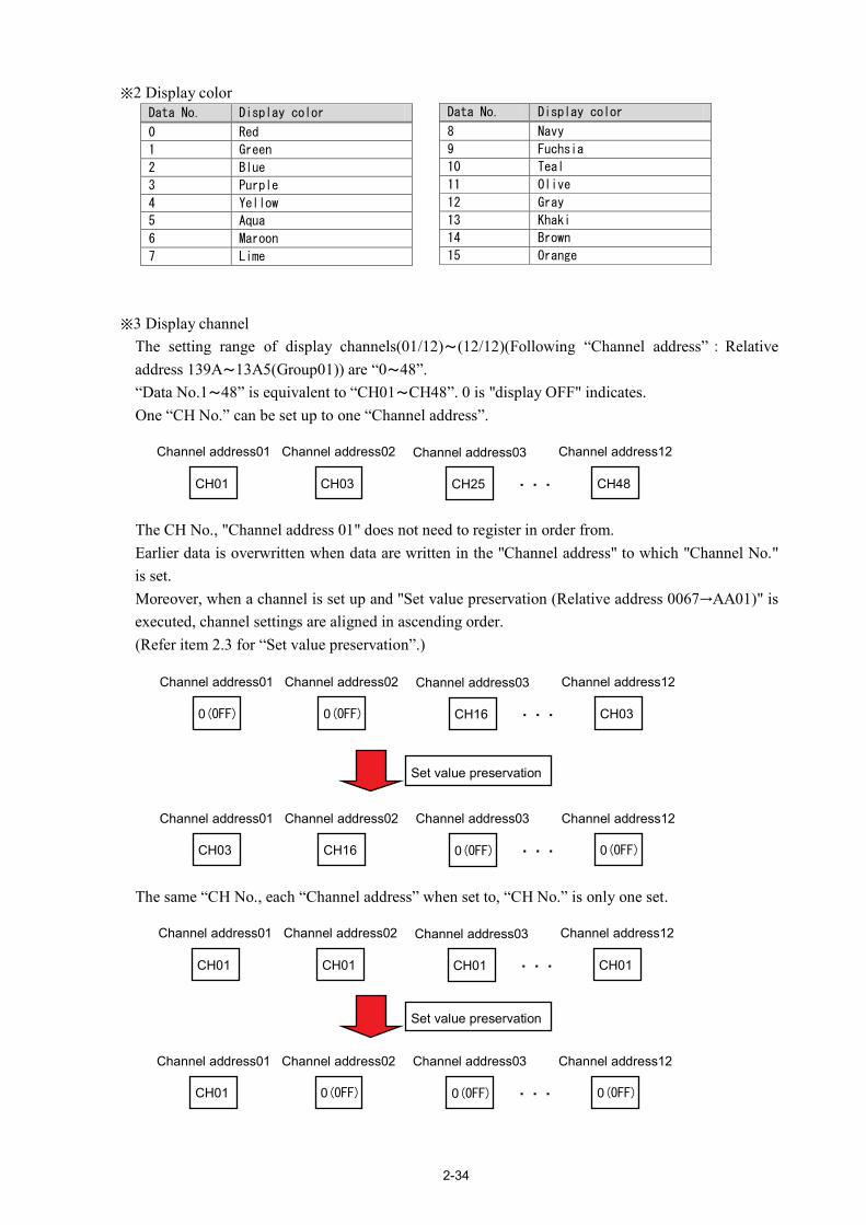
※2 Display color Data No. Display color
0 Red
1 Green
2 Blue
3 Purple
4 Yellow
5 Aqua
6 Maroon
7 Lime
※3 Display channel The setting range of display channels(01/12)~(12/12)(Following “Channel address”:Relative address 139A~13A5(Group01)) are “0~48”. “Data No.1~48” is equivalent to “CH01~CH48”. 0 is "display OFF" indicates. One “CH No.” can be set up to one “Channel address”.
The CH No., "Channel address 01" does not need to register in order from. Earlier data is overwritten when data are written in the "Channel address" to which "Channel No." is set. Moreover, when a channel is set up and "Set value preservation (Relative address 0067→AA01)" is executed, channel settings are aligned in ascending order. (Refer item 2.3 for “Set value preservation”.)
The same “CH No., each “Channel address” when set to, “CH No.” is only one set.
Data No. Display color
8 Navy
9 Fuchsia
10 Teal
11 Olive
12 Gray
13 Khaki
14 Brown
15 Orange
CH48
Channel address12
・・・
Set value preservation
CH25
Channel address03
CH03
Channel address02
CH01
Channel address01
CH03
Channel address12
・・・ CH16
Channel address03
0(OFF)
Channel address02
0(OFF)
Channel address01
0(OFF)
Channel address12
・・・ 0(OFF)
Channel address03
CH16
Channel address02
CH03
Channel address01
CH01
Channel address12
・・・ CH01
Channel address03
CH01
Channel address02
CH01
Channel address01
Set value preservation
0(OFF)
Channel address12
・・・ 0(OFF)
Channel address03
0(OFF)
Channel address02
CH01
Channel address01

2-35
※4 Record cycle Data No. Record cycle
1 100ms (Sub record only)
2 1sec
3 2sec
4 3sec
5 5sec
6 10sec
7 15sec
8 20sec
9 30sec
10 1min
11 2min
12 3min
13 5min
14 10min
15 15min
16 20min
17 30min
18 60min
※5 File record cycle The "File record cycle" depends on the "Record cycle".
Data No. File record cycle Record cycle
1 1 hour 100ms~5sec
2 1 hour, 1 day 10sec~1min
3 1 hour, 1 day, 1 week 2min~3min
4 1 hour, 1 day, 1 week, 1 month 5min~30min
5 1 hour, 1 day, 1 week, 1 month, 1 year 60min
※6 Sub record timing System Settings “Device / Other” ⇒ “FUNC key” is “OFF” only when you can choose “1:Func key”. (Refer item 7.20 or 8.15 of Paperless Recorder Manual (WXPVM70mnA0001E) for details.)
Data No. Sub record timing
0 OFF
1 Func key
2 Alarm
3 DI
4 Sync.
※7 IP Address, Subnet Mask, Default GW, DNS address “IP Address (01/03)” and “IP address (02/03)” is a pair. (“IP Address (03/03)” is not used.) Ex) IP Address set “192.168.0.1”. 192. 168. 0. 1
Enter the IP address by HEX. 192(DEC) = C0(HEX)、168(DEC) = A8(HEX) ⇒【IP Address(01/03)】:C0A8 0(DEC) = 00(HEX)、1(DEC) = 01(HEX) ⇒【IP Address(02/03)】:0001
【IP Address(01/03)】 【IP Address(02/03)】

2-36
※8 Time zone (UTC) Data No. Time zone (UTC)
0 -12:00
1 -11:00
2 -10:00
3 -09:00
4 -08:00
5 -07:00
6 -06:00
7 -05:00
8 -04:00
9 -03:00
10 -02:00
11 -01:00
12 +00:00
13 +01:00
14 +02:00
15 +03:00
※9 SNTP manual calibration Time is calibrated by SNTP function. (Only record stop) The result of SNTP manual calibration can get by reading the same address "006E." (Status response value) ● The check on a Modbus protocol ①Data receive only "0000H" or "AA01H". (The other command becomes a command error.) ②When data is "0000H", "0000H" is set as a status response value. (Manual calibration is not started.) ③Calibrate when data is "AA01H", and the following conditions are satisfied.
・The last status response value = 0000H ・"SNTP function" of System is "ON". ・Main record is not started.
Manual calibration is started. A status response value becomes "5500H". ※ Setting of SNTP uses what is beforehand set up by the recorder.
(Refer item 8.8 of Paperless Recorder Manual for SNTP function.) ● The status response after a SNTP manual calibration reception.
A status response is as follows. (A communication state continues for a maximum of 30 seconds.) 5500H = Now communicating 5501H = Calibration success 5510H = Link down 5511H = DNS error 5512H = Address error 5513H = Time out 0000H = SNTP reception preparation completion (When 0000H is received.)
※ In order to check completion of action, please wait until a status response becomes except for "5500H" or "0000H".
Data No. Time zone (UTC)
16 +04:00
17 +05:00
18 +06:00
19 +07:00
20 +08:00
21 +09:00
22 +10:00
23 +11:00
24 +12:00
25 +13:00
26 +14:00
27 +04:30
28 +05:45
29 +05:30
30 +09:30

2-37
※10 Parameter save (Recorder → SD) The current parameter and system state is saved to an SD card. The result of save of parameter can get by reading the same address "006F". (Status response value)
(A file name is "modprm.dps" fixation. Keep the file of a same name from existing on an SD card. Moreover, it becomes an error if a file already exists. Please save after deleting a file previously.)
● The check on a Modbus protocol ①Data receive only "0000H" or "AA01H". (The other command becomes a command error.) ②When data is "0000H", "0000H" is set as a status response value.(Save of parameter is not
started.) ③Save the parameter when data is "AA01H", and the following conditions are satisfied. ・The last status response value of parameter read = 0000H ・The last status response value of parameter write = 0000H ・The SD card is inserted. Save of parameter is started. A status response value becomes "5500H".
● The status response after a save of parameter. A status response is as follows.
5500H = Now writing 5501H = Writing success 5510H = A file already exists. 5511H = File writing error 0000H = "Write of parameter" preparation completion
※ In order to check completion of action, please wait until a status response becomes except for "5500H" or "0000H".
※11 Parameter load (SD → Recorder)
A parameter file (DPS file) is written to recorder from a host computer by FTP, and it is read with a recorder.(A file name is "modprm.dps" fixation.) The result of read of parameter can get by reading the same address "0070." (Status response value)
● The check on a Modbus protocol ①Data receive only "0000H" or "AA01H". (The other command becomes a command error.) ②When data is "0000H", "0000H" is set as a status response value.(Read of parameter is not
started.) ③Read of parameter when data is "AA01H", and the following conditions are satisfied.
・The last status response value of parameter read = 0000H ・The last status response value of parameter write = 0000H ・The SD card is inserted. ・Main record is not started.
Read of parameter is started. A status response value becomes "5500H". ● The status response after a read of parameter.
A status response is as follows. 5500H = Now reading 5501H = Reading success 5510H = A file already exists. 5511H = File reading error 0000H = "Read of parameter" preparation completion
※ In order to check completion of action, please wait until a status response becomes except for "5500H" or "0000H".