vlsiアーキテクチャ 4 坂井 修一sakai/vlsi/vlsi4.pdfvlsiアーキテクチャ...
TRANSCRIPT

東大・電気VLSIアーキテクチャ
VLSIアーキテクチャ(4)
坂井 修一東京大学大学院 情報理工学系研究科電子情報学専攻
東京大学 工学部電子情報工学科/電気工学科
工学部講義
• はじめに
• CPUの設計(3)

はじめに 本講義の目的
– VLSIアーキテクチャの基本を学ぶ: 機能 ⇒ VLSI
対象者: 工学部4年生以上
担当者– 坂井修一 プロセッサ → VLSI
– 池田 誠 アルゴリズム→ VLSI
時間・場所– 水曜日 8:30 - 10:15
– 工学部2号館243
前提となる知識– 電気回路、電子回路
– ディジタル論理回路
– 半導体デバイス、VLSI
– コンピュータアーキテクチャ
VLSIアーキテクチャ 東大・電気

教科書、成績
教科書– 坂井修一『実践 コンピュータアーキテクチャ』(コロナ社)
坂井部分は教科書通りやります
– (池田先生の教科書)
参考書: 電子デバイス、論理回路、コンピュータアーキテクチャ– 坂井修一『論理回路入門』、培風館
– 坂井修一『コンピュータアーキテクチャ』、コロナ社
– 電子回路、VLSI
(池田先生推薦の本)
http://www.mtl.t.u-tokyo.ac.jp/~sakai/vlsi/
成績– 実習レポート+出席
VLSIアーキテクチャ 東大・電気

講義の概要と予定
VLSIアーキテクチャ入門
– 坂井 4/11
CPU設計論
– 坂井 4/18, 5/9, 16, 6/13 (5/16 レポート出題)
専用回路設計論
– 池田 4/25, 5/2, 23, 6/6, 27
まとめ・将来展望
– 坂井 6/20
– 池田 7/4
予備 7/11
VLSIアーキテクチャ

CPUの構成と設計の基本方針(復習)
VLSIアーキテクチャ 東大・電気
データメモリ
データ選択
命
令
演算制御
命令デコーダ
選択回路
PC
命令メモリ
レジスタファイル(読み)
レジスタアドレス デ
ータ選択
+
ALU
即値
メモリアドレス
データメモリ変位
メモリアドレス
メモリ制御
レジスタファイル(書き)
命令メモリ変位0
+ PC
セット
命令アドレス
①命令フェッチ(F) ②命令デコード(D) ③演算実行(E) ④結果格納(W)
アドレスの流れ 制御の流れ データの流れ
1
フラグ
動作に着目したプロセッサの内部構成
設計方針
(1) 上位モジュールは「動作」を基本とし、①命令フェッチ、②命令デコード、③実行、④結果の格納をそれぞれモジュールとして設計する。
(2) 下位モジュールは「ハードウェアの実体」に近いものとする。

シミュレーションによる検証 シミュレーションによる動作検証:方法と手順
– Modelsim: Verilogテストモジュールを用いる
– 要素から全体へ
• 単純なモジュールや関数のシミュレーション
• 上位モジュールのシミュレーション
• トップモジュールのシミュレーション
• 実応用の(に近い)シミュレーション
階層構造
VLSIアーキテクチャ 東大・電気
computer fetch
data_mem
execute opr_gen
alu
wrengen
wreg
calc
npc
writeback
regr_file

構成要素 (1): 命令フェッチ部
命令フェッチ部
– アセンブラによる機械語プログラム生成
– ファイルからの機械語プログラムのロード
• $readmemb
– フェッチ動作: 命令メモリの読み出し
• fetch, $monitor
– Modelsimによるメモリ内容の表示
VLSIアーキテクチャ 東大・電気

アセンブラによる機械語プログラムの生成
VLSIアーキテクチャ 東大・電気
addi r1, r0, 1addi r2, r1, 1 アセンブラ プログラム (1+1=2)
> perl asm.pl sample.asm > sample.bnr>
Windows コマンドによるアセンブル
000001_00000_00001_0000000000000001_000001_00001_00010_0000000000000001_
ファイル名: sample.bnr
機械語プログラム

機械語プログラムのロード
VLSIアーキテクチャ 東大・電気
module fetch(pc, ins);input [31:0] pc;output [31:0] ins;reg [31:0] ins_mem [0:255];
assign ins = ins_mem[pc] ;initial$readmemb("sample.bnr", ins_mem [0:255]);
endmodule
$readmemb(“filename”, array);⇒ filenameのファイルからarrayにデータを読み込む

フェッチ動作のテスト
VLSIアーキテクチャ 東大・電気
module tfetch;reg clk, rst;reg [31:0] pc;wire [31:0] ins;
initialbeginclk = 0; forever #50 clk = !clk;
end
initialbegin
rstd = 1;#10 rst = 0;#20 rst = 1;
end
always @(negedge rst or posedge clk)begin
if (rst == 0) pc <= 0;else if (clk == 1) pc <= pc + 1;
end
initial$monitor($stime, "¥rstd=%b, clk=%b, pc=%d, ins=%b", rstd, clk, pc, ins);
fetch fetch_body(pc, ins);endmodule
列挙した信号に変化があればプリントする

テスト結果
VLSIアーキテクチャ 東大・電気
VSIM1> run# 0 rstd=1, clk=0, pc= x, ins=xxxxxxxxxxxxxxxxxxxxxxxxxxxxxxxx# 10 rstd=0, clk=0, pc= 0, ins=00000100000000010000000000000001# 30 rstd=1, clk=0, pc= 0, ins=00000100000000010000000000000001# 50 rstd=1, clk=1, pc=1, ins=00000100001000100000000000000001# 100 rstd=1, clk=0, pc= 1, ins=00000100001000100000000000000001# 150 rstd=1, clk=1, pc=2, ins=xxxxxxxxxxxxxxxxxxxxxxxxxxxxxxxx

Modelsimによるメモリ内容の表示
VLSIアーキテクチャ 東大・電気
WorkspaceウィンドウのMemoriesタブをクリックして表示させる

構成要素のシミュレーション(2)
実行部
– 演算回路• ALU演算の指定回路(opr_gen): 組合せ回路の場合を
尽くす
• ALU: case文 → 場合の数が多い– 典型的なパターンと極端なパターンのテスト
– プログラム実行によるテスト
• 結果データの生成・分岐・書き込みレジスタの選択:case文が多い
– ALUと同様の方法でテスト
VLSIアーキテクチャ 東大・電気

opr_genのテスト: 演算を決定する回路
VLSIアーキテクチャ 東大・電気
module test_opr_gen;reg [5:0] op;reg [4:0] operation;reg [4:0] opr;
function [4:0] opr_gen;input [5:0] op;input [4:0] operation;case (op)6'd0: opr_gen = operation;6'd1: opr_gen = 5'd0;6'd4: opr_gen = 5'd8;6'd5: opr_gen = 5'd9;6'd6: opr_gen = 5'd10;default: opr_gen = 5'h1f;endcaseendfunction
initialbegin
op = 6'd0; operation = 5'd0; opr = opr_gen(op, operation);#100 op = 6'd0; operation = 5'd8; opr = opr_gen(op, operation);#100 op = 6'd0; operation = 5'd11; opr = opr_gen(op, operation);#100 op = 6'd1; operation = 5'd0; opr = opr_gen(op, operation);#100 op = 6'd4; operation = 5'd3; opr = opr_gen(op, operation);#100 op = 6'd5; operation = 5'd9; opr = opr_gen(op, operation);#100 op = 6'd6; operation = 5'd11; opr = opr_gen(op, operation);#100 op = 6'd2; operation = 5'd0; opr = opr_gen(op, operation);#100 op = 6'd10; operation = 5'd11; opr = opr_gen(op, operation);
end
initial$monitor($stime, " op=%d, operation=%d, opr=%d", op, operation, opr);
endmodule
100ユニットごとに異なる入力を与える
列挙した信号に変化があればプリントする

opr_genのテスト結果
VLSIアーキテクチャ 東大・電気
VSIM1> run# 0 op= 0, operation= 0, opr= 0# 100 op= 0, operation= 8, opr= 8# 200 op= 0, operation=11, opr=11# 300 op= 1, operation= 0, opr= 0# 400 op= 4, operation= 3, opr= 8# 500 op= 5, operation= 9, opr= 9# 600 op= 6, operation=11, opr=10# 700 op= 2, operation= 0, opr=31# 800 op=10, operation=11, opr=31

ALUのテスト
VLSIアーキテクチャ 東大・電気
module test_alu;reg[4:0] operation, shift;reg [31:0] operand1, operand2, result;
function [31:0] alu;前述の通り
endfunction
initialbegin
opr = 0; shift = 0;operand1=32'h00000000;operand2=32'h00000000;result = alu(opr, shift, operand1,operand2);#100 operand1 = 32'h00000000; operand2 = 32'h00000001; result = alu(opr, shift, operand1,operand2);#100 operand1 = 32'h0fffffff; operand2 = 32'h00000001; result = alu(opr, shift, operand1,operand2);#100 operand1 = 32'hffffffff; operand2 = 32'hffffffff; result = alu(opr, shift, operand1,operand2);#100 opr = 1; operand1 = 32'h00000000; operand2 = 32'h00000000;result = alu(opr,shift, operand1,operand2);#100 operand1 = 32'hffffffff; operand2 = 32'hfffffffe; result = alu(opr, shift, operand1,operand2);#100 opr = 8;operand1 = 32'h00000000; operand2 = 32'hffffffff; result = alu(opr, shift, operand1,operand2);#100 operand1 = 32'h55555555; operand2 = 32'haaaaaaaa; result = alu(opr, shift, operand1,operand2);#100 operand1 = 32‘hffffffff; operand2 = 32’hffffffff; result = alu(opr, shift, operand1,operand2);#100 opr = 9;operand1 = 32'h00000000; operand2 = 32'hffffffff; result = alu(opr, shift, operand1,operand2);#100 operand1 = 32'h55555555; operand2 = 32'haaaaaaaa; result = alu(opr, shift, operand1,operand2);#100 opr = 10;operand1 = 32'h00000000; operand2 = 32'hffffffff; result = alu(opr, shift, operand1,operand2);#100 operand1 = 32'h55555555; operand2 = 32'h55555555; result = alu(operand1,operand2, opr, shift);#100 opr = 11;operand1 = 32'h00000000; operand2 = 32'hffffffff; result = alu(opr, shift, operand1,operand2);#100 operand1 = 32'h55555555; operand2 = 32'h55555555; result = alu(operand1,operand2, opr, shift);#100 opr = 16;operand1 = 32'h12345678; shift = 2'h1; result = alu(opr, shift, operand1,operand2);#100 opr = 16;operand1 = 32'h12345678; shift = 2'h1; result = alu(opr, shift, operand1,operand2);#100 opr = 17;operand1 = 32'h12345678; shift = 2'h1; result = alu(opr, shift, operand1,operand2);#100 opr = 18;operand1 = 32'h12345678; shift = 2'h1; result = alu(operand1,operand2, opr, shift);
#100 operand1 = 32'h92345678; shift = 2'h1; result = alu(opr, shift, operand1,operand2);#100 opereation = 2; result = alu(opr, shift, operand1,operand2);
end
initial$monitor($stime, " op=%h, shift=%h, op1=%h, op2=%h, result=%h", opr, shift, operand1, operand2, result);
endmodule
100ユニットごとに異なる入力を与える
列挙した信号に変化があればプリントする

ALUのテスト結果
VLSIアーキテクチャ 東大・電気
> VSIM5 run -all# 0 op=00, shift=00, op1=00000000, op2=00000000, result=00000000# 100 op=00, shift=00, op1=00000000, op2=00000001, result=00000001# 200 op=00, shift=00, op1=0fffffff, op2=00000001, result=10000000# 300 op=00, shift=00, op1=ffffffff, op2=ffffffff, result=fffffffe# 400 op=01, shift=00, op1=00000000, op2=00000000, result=00000000# 500 op=01, shift=00, op1=ffffffff, op2=fffffffe, result=00000001# 600 op=08, shift=00, op1=00000000, op2=ffffffff, result=00000000# 700 op=08, shift=00, op1=55555555, op2=aaaaaaaa, result=00000000# 800 op=08, shift=00, op1=ffffffff, op2=ffffffff, result=ffffffff# 900 op=09, shift=00, op1=00000000, op2=ffffffff, result=ffffffff# 1000 op=09, shift=00, op1=55555555, op2=aaaaaaaa, result=ffffffff# 1100 op=0a, shift=00, op1=00000000, op2=ffffffff, result=ffffffff# 1200 op=0a, shift=00, op1=55555555, op2=55555555, result=ffffffff# 1300 op=0b, shift=00, op1=00000000, op2=ffffffff, result=ffffffff# 1400 op=0b, shift=00, op1=55555555, op2=55555555, result=ffffffff# 1500 op=10, shift=01, op1=12345678, op2=55555555, result=2468acf0# 1700 op=11, shift=01, op1=12345678, op2=55555555, result=091a2b3c# 1800 op=12, shift=01, op1=12345678, op2=55555555, result=ffffffff# 1900 op=12, shift=01, op1=92345678, op2=55555555, result=491a2b3c# 2000 op=02, shift=01, op1=92345678, op2=55555555, result=ffffffff
ALUのテスト → プログラムでテストパターンを生成し、結果パターンを別途作成しておいてプログラムで照合するなどの方法を採るのが一般的

結果データの生成・分岐・書き込みレジスタの選択
結果データの生成
分岐
書き込みレジスタの選択
– すべてcase文で与えられる組み合わせ回路
→ ALUと同様の方法でシミュレーションする
VLSIアーキテクチャ 東大・電気

構成要素のシミュレーション(3)
データメモリ読み書き– 書き込んだデータを読み出す
書き戻し部– PCのリセットまたは+1: 場合を尽くす (簡単な回路)
レジスタファイル– データメモリのシミュレーションと同様に読み書きのシミュレーショ
ン
– ポート間同時アクセスのシミュレーション、チェック
VLSIアーキテクチャ 東大・電気

データメモリのテスト
VLSIアーキテクチャ 東大・電気
module data_mem(address, clk, write_data, wren, read_data);図7.9と同じ
module test_mem;reg[7:0] address;reg clk, wren;
reg [31:0] ra, wa, write_datawire [31:0] read_data;
initial beginclk = 0; forever #50 clk = ~clk;end
initialbegin
#40 address = 0; write_data=8'h21; wren = 0;#100 address = 1; write_data=8'h43; wren = 0;#100 address = 2; write_data = 8'h65; wren = 1;#100 address = 2; write_data = 8'h87; wren = 0;#100 address = 3; write_data = 8'ha9; wren = 0;#100 address = 0; wren = 1;#100 address = 1; wren = 1;#100 address = 2; wren = 1;#100 address = 3; wren = 1;
end
initial $monitor($stime, "address=%d, clk=%d, write_data=%h, wren=%d,read_data=%h", address, clk, write_date, read_data);
data_mem data_mem_body(address, clk, write_data, wren, read_data))endmodule
1クロックごとにメモリに異なる入力を与える
列挙した信号に変化があればプリントする

データメモリのテスト結果
VLSIアーキテクチャ 東大・電気
isim1> run# 0 address= x, clk=0, write_data=xx, wren=x, read_data=xx# 40 address= 0, clk=0, write_data=21, wren=0, read_data=xx# 50 address= 0, clk=1, write_data=21, wren=0, read_data=21# 100 address= 0, clk=0, write_data=21, wren=0, read_data=21# 140 address= 1, clk=0, write_data=43, wren=0, read_data=xx# 150 address= 1, clk=1, write_data=43, wren=0, read_data=43# 200 address= 1, clk=0, write_data=43, wren=0, read_data=43# 240 address= 2, clk=0, write_data=65, wren=1, read_data=xx# 250 address= 2, clk=1, write_data=65, wren=1, read_data=xx# 300 address= 2, clk=0, write_data=65, wren=1, read_data=xx# 340 address= 2, clk=0, write_data=87, wren=0, read_data=xx# 350 address= 2, clk=1, write_data=87, wren=0, read_data=87# 400 address= 2, clk=0, write_data=87, wren=0, read_data=87# 440 address= 3, clk=0, write_data=a9, wren=0, read_data=xx# 450 address= 3, clk=1, write_data=a9, wren=0, read_data=a9# 500 address= 3, clk=0, write_data=a9, wren=0, read_data=a9# 540 address= 0, clk=0, write_data=a9, wren=1, read_data=21# 550 address= 0, clk=1, write_data=a9, wren=1, read_data=21# 600 address= 0, clk=0, write_data=a9, wren=1, read_data=21# 640 address= 1, clk=0, write_data=a9, wren=1, read_data=43# 650 address= 1, clk=1, write_data=a9, wren=1, read_data=43# 700 address= 1, clk=0, write_data=a9, wren=1, read_data=43# 740 address= 2, clk=0, write_data=a9, wren=1, read_data=87# 750 address= 2, clk=1, write_data=a9, wren=1, read_data=87# 800 address= 2, clk=0, write_data=a9, wren=1, read_data=87# 840 address= 3, clk=0, write_data=a9, wren=1, read_data=a9# 850 address= 3, clk=1, write_data=a9, wren=1, read_data=a9
00000000 2100000001 4300000002 8700000003 a900000004 xx
メモリの中身

構成要素のシミュレーション(4)
書き戻し部
– PCのリセットまたは+1: 場合を尽くす (簡単な回路)
VLSIアーキテクチャ 東大・電気

書き戻し部のテスト
VLSIアーキテクチャ 東大・電気
module test_writeback;reg clk, rstd;reg [31:0] nextpc;wire [31:0] pc;
initialbeginclk = 0; forever #50 clk = ~clk;
end
initialbegin
rstd = 1;#10 rstd = 0;#20 rstd = 1;end
initialbegin#30 nextpc = 0'h00000001;#100 nextpc = 0'h12345678;#100 nextpc = 0'h87654321;#100 nextpc = 0'hffffffff;
end
writeback writeback_body(clk, rstd, nextpc, pc);
initial $monitor($stime, " rstd=%d, clk=%d, nextpc=%h, pc=%h", rstd, clk, nextpc, pc);endmodule
1クロックごとに異なる入力を与える
列挙した信号に変化があればプリントする
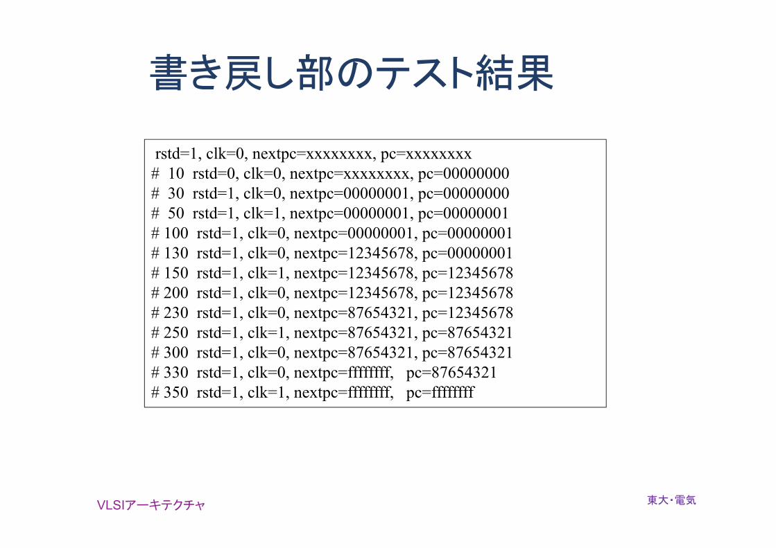
書き戻し部のテスト結果
VLSIアーキテクチャ 東大・電気
rstd=1, clk=0, nextpc=xxxxxxxx, pc=xxxxxxxx# 10 rstd=0, clk=0, nextpc=xxxxxxxx, pc=00000000# 30 rstd=1, clk=0, nextpc=00000001, pc=00000000# 50 rstd=1, clk=1, nextpc=00000001, pc=00000001# 100 rstd=1, clk=0, nextpc=00000001, pc=00000001# 130 rstd=1, clk=0, nextpc=12345678, pc=00000001# 150 rstd=1, clk=1, nextpc=12345678, pc=12345678# 200 rstd=1, clk=0, nextpc=12345678, pc=12345678# 230 rstd=1, clk=0, nextpc=87654321, pc=12345678# 250 rstd=1, clk=1, nextpc=87654321, pc=87654321# 300 rstd=1, clk=0, nextpc=87654321, pc=87654321# 330 rstd=1, clk=0, nextpc=ffffffff, pc=87654321# 350 rstd=1, clk=1, nextpc=ffffffff, pc=ffffffff

構成要素のシミュレーション(5)
レジスタファイル
– データメモリのシミュレーションと同様に読み書きのシミュレーション
– ポート間同時アクセスのシミュレーション、チェック
VLSIアーキテクチャ 東大・電気

レジスタファイルのテスト
VLSIアーキテクチャ 東大・電気
module test_register_file;reg clk, rstd, wren;reg [4:0] ra1, ra2, wa;wire [31:0] rr1, rr2;reg [31:0] wr;
initialbegin
clk = 0; forever #50 clk = !clk;end
initialbegin
rstd = 1;#30 rstd = 0;#40 rstd = 1;
#10 wren=0; ra1=1; ra2=2; wa=3; wr=32'haaaaaaaa;#100 ra1=3; ra2=3; wa=4; wr=32'h55555555;#100 ra1=4; ra2=5; wa=5; wr=32'h12345678;#100 ra1=5; ra2=4; wa=6; wr=32'h87654321;#100 ra1=6; ra2=0; wa=1; wr=32'h11111111;#100 ra1=1; ra2=6; wa=2; wr=32'h22222222;#100 ra1=1; ra2=2; wa=7; wr=32'h77777777;#100 wren=1; ra1=1; ra2=2; wa=8; wr=32'haaaaaaaa;#100 ra1=3; ra2=4; wa=9; wr=32'h11111111;#100 ra1=5; ra2=6; wa=10; wr=32'hbbbbbbbb;#100 ra1=7; ra2=8; wa=11; wr=32'hcccccccc;#100 ra1=9; ra2=10; wa=11; wr=32'hdddddddd;
// #100 ....end
reg_file rf_body(clk, rstd, wr, ra1, ra2, wa, wren, rr1, rr2);
initial$monitor($stime, " clk=%d, rstd=%d, ra1=%h, ra2=%h, wa=%h, rr1=%h,
rr2=%h, wr=%h, wren=%h", clk, rstd, ra1, ra2, wa, rr1, rr2, wr, wren);endmodule
1クロックごとに異なる入力を与える
列挙した信号に変化があればプリントする

レジスタファイルのテスト結果
VLSIアーキテクチャ 東大・電気
Vsim > run# 0 clk=0, rstd=1, ra1=xx, ra2=xx, wa=xx, rr1=xxxxxxxx, rr2=xxxxxxxx, wr=xxxxxxxx, wren=x# 30 clk=0, rstd=0, ra1=xx, ra2=xx, wa=xx, rr1=xxxxxxxx, rr2=xxxxxxxx, wr=xxxxxxxx, wren=x# 50 clk=1, rstd=0, ra1=xx, ra2=xx, wa=xx, rr1=xxxxxxxx, rr2=xxxxxxxx, wr=xxxxxxxx, wren=x# 70 clk=1, rstd=1, ra1=xx, ra2=xx, wa=xx, rr1=xxxxxxxx, rr2=xxxxxxxx, wr=xxxxxxxx, wren=x# 80 clk=1, rstd=1, ra1=01, ra2=02, wa=03, rr1=xxxxxxxx, rr2=xxxxxxxx, wr=aaaaaaaa, wren=0# 100 clk=0, rstd=1, ra1=01, ra2=02, wa=03, rr1=xxxxxxxx, rr2=xxxxxxxx, wr=aaaaaaaa, wren=0# 150 clk=1, rstd=1, ra1=01, ra2=02, wa=03, rr1=xxxxxxxx, rr2=xxxxxxxx, wr=aaaaaaaa, wren=0# 180 clk=1, rstd=1, ra1=03, ra2=03, wa=04, rr1=aaaaaaaa, rr2=aaaaaaaa, wr=55555555, wren=0# 200 clk=0, rstd=1, ra1=03, ra2=03, wa=04, rr1=aaaaaaaa, rr2=aaaaaaaa, wr=55555555, wren=0# 250 clk=1, rstd=1, ra1=03, ra2=03, wa=04, rr1=aaaaaaaa, rr2=aaaaaaaa, wr=55555555, wren=0# 280 clk=1, rstd=1, ra1=04, ra2=05, wa=05, rr1=55555555, rr2=xxxxxxxx, wr=12345678, wren=0# 300 clk=0, rstd=1, ra1=04, ra2=05, wa=05, rr1=55555555, rr2=xxxxxxxx, wr=12345678, wren=0# 350 clk=1, rstd=1, ra1=04, ra2=05, wa=05, rr1=55555555, rr2=12345678, wr=12345678, wren=0# 380 clk=1, rstd=1, ra1=05, ra2=04, wa=06, rr1=12345678, rr2=55555555, wr=87654321, wren=0# 400 clk=0, rstd=1, ra1=05, ra2=04, wa=06, rr1=12345678, rr2=55555555, wr=87654321, wren=0# 450 clk=1, rstd=1, ra1=05, ra2=04, wa=06, rr1=12345678, rr2=55555555, wr=87654321, wren=0# 480 clk=1, rstd=1, ra1=06, ra2=00, wa=01, rr1=87654321, rr2=00000000, wr=11111111, wren=0# 500 clk=0, rstd=1, ra1=06, ra2=00, wa=01, rr1=87654321, rr2=00000000, wr=11111111, wren=0# 550 clk=1, rstd=1, ra1=06, ra2=00, wa=01, rr1=87654321, rr2=00000000, wr=11111111, wren=0# 580 clk=1, rstd=1, ra1=01, ra2=06, wa=02, rr1=11111111, rr2=87654321, wr=22222222, wren=0# 600 clk=0, rstd=1, ra1=01, ra2=06, wa=02, rr1=11111111, rr2=87654321, wr=22222222, wren=0# 650 clk=1, rstd=1, ra1=01, ra2=06, wa=02, rr1=11111111, rr2=87654321, wr=22222222, wren=0# 680 clk=1, rstd=1, ra1=01, ra2=02, wa=07, rr1=11111111, rr2=22222222, wr=77777777, wren=0# 700 clk=0, rstd=1, ra1=01, ra2=02, wa=07, rr1=11111111, rr2=22222222, wr=77777777, wren=0# 750 clk=1, rstd=1, ra1=01, ra2=02, wa=07, rr1=11111111, rr2=22222222, wr=77777777, wren=0# 780 clk=1, rstd=1, ra1=01, ra2=02, wa=08, rr1=11111111, rr2=22222222, wr=aaaaaaaa, wren=1# 800 clk=0, rstd=1, ra1=01, ra2=02, wa=08, rr1=11111111, rr2=22222222, wr=aaaaaaaa, wren=1# 850 clk=1, rstd=1, ra1=01, ra2=02, wa=08, rr1=11111111, rr2=22222222, wr=aaaaaaaa, wren=1# 880 clk=1, rstd=1, ra1=03, ra2=04, wa=09, rr1=aaaaaaaa, rr2=55555555, wr=11111111, wren=1# 900 clk=0, rstd=1, ra1=03, ra2=04, wa=09, rr1=aaaaaaaa, rr2=55555555, wr=11111111, wren=1# 950 clk=1, rstd=1, ra1=03, ra2=04, wa=09, rr1=aaaaaaaa, rr2=55555555, wr=11111111, wren=1# 980 clk=1, rstd=1, ra1=05, ra2=06, wa=0a, rr1=12345678, rr2=87654321, wr=bbbbbbbb, wren=1#1000 clk=0, rstd=1, ra1=05, ra2=06, wa=0a, rr1=12345678, rr2=87654321, wr=bbbbbbbb, wren=1#1050 clk=1, rstd=1, ra1=05, ra2=06, wa=0a, rr1=12345678, rr2=87654321, wr=bbbbbbbb, wren=1#1080 clk=1, rstd=1, ra1=07, ra2=08, wa=0b, rr1=77777777, rr2=xxxxxxxx, wr=cccccccc, wren=1#1100 clk=0, rstd=1, ra1=07, ra2=08, wa=0b, rr1=77777777, rr2=xxxxxxxx, wr=cccccccc, wren=1#1150 clk=1, rstd=1, ra1=07, ra2=08, wa=0b, rr1=77777777, rr2=xxxxxxxx, wr=cccccccc, wren=1#1180 clk=1, rstd=1, ra1=09, ra2=0a, wa=0b, rr1=xxxxxxxx, rr2=xxxxxxxx, wr=dddddddd, wren=1#1200 clk=0, rstd=1, ra1=09, ra2=0a, wa=0b, rr1=xxxxxxxx, rr2=xxxxxxxx, wr=dddddddd, wren=1#1250 clk=1, rstd=1, ra1=09, ra2=0a, wa=0b, rr1=xxxxxxxx, rr2=xxxxxxxx, wr=dddddddd, wren=1#1300 clk=0, rstd=1, ra1=09, ra2=0a, wa=0b, rr1=xxxxxxxx, rr2=xxxxxxxx, wr=dddddddd, wren=1

全体シミュレーション
信号レベルのシミュレーション– ブレークポイントを設定して信号線やメモリセルの値を観察する
– システムタスクを利用して、重要な信号の変化を表示させる
命令実行のシミュレーション– すべての命令が仕様通り稼働するか?
– 命令の続き具合に依存する誤動作がないか?
プログラムのシミュレーション– アセンブリ言語でプログラムを書く
– アセンブル
– 命令メモリにプログラムをロードする(命令フェッチ部のテストと同じ)
– Modelsimでシミュレーション実行
コンピュータアーキテクチャ 東大・坂井

トップモジュール (HDL記述)
VLSIアーキテクチャ 東大・電気
module computer(clk, rstd);input clk, rstd;wire [31:0] pc, ins, reg1,reg2, result, nextpc;wire [4:0] wra;wire [3:0] wren;
fetch fetch_body (pc[7:0], ins);execute execute_body (clk, ins, pc, reg1, reg2, wra, result, nextpc);writeback writeback_body (clk, rstd, nextpc, pc);reg_file rf_body (clk, rstd, result, ins[25:21], ins[20:16], wra, (~| wra), reg1, reg2);
endmodule

トップモジュールのシミュレーション
VLSIアーキテクチャ 東大・電気
module tcomputer3;reg clk, rstd;
initialbegin rstd =1;#10 rst = 0;#10 rst = 1;
end
initialbegin clk = 0; forever #50 clk = ~clk;end
computer computer3_body(clk, rst);endmodule
initial $monitor($time, " rstd=%d, clk=%d, pc=%h, ins=%h, reg1=%h, reg2=%h",rstd, clk, pc, ins, reg1, reg2);
重要な信号変化の表示: computerに入れておく
クロック毎の動作をシミュレートする
プログラムは別途命令メモリに入れておく

1+1=2 のシミュレーション結果
VLSIアーキテクチャ 東大・電気

階和計算のプログラム
VLSIアーキテクチャ 東大・電気
addi r1, r0, 20addi r2, r0, 0addi r3, r0, 0
label: addi r2, r2, 1add r3, r2, r3blt r2 r1 label
end: j end
N=20
000001_00000_00001_0000000000010100_000001_00000_00010_0000000000000000_000001_00000_00011_0000000000000000_000001_00010_00010_0000000000000001_000000_00010_00011_00011_00000000000_100010_00010_00001_1111111111111101_101000_00000000000000000000000110_
アセンブル

階和計算のシミュレーション結果
VLSIアーキテクチャ 東大・電気
1+2+3+…+20 = 210 = 11010010(binary) (R3の値)

宿題4 この授業で作成したプロセッサをVerilog HDLで記述せよ
教科書にしたがって、次の各モジュールをシミュレーションせよ– 命令フェッチ部
– 実行部: ALU
– データメモリ読み書き
– 書き戻し部
– レジスタファイル
教科書にしたがって、1+1=2などのプログラムをシミュレータ上で動作させよ
提出の必要はないが、次のレポート課題のためには必須となる。
VLSIアーキテクチャ 東大・電気

レポート課題(別紙)
提出
6月29日(金)17時まで
に
電気系事務室
レポートボックスへ
遅れた場合は理由のいかんによらず受理しませんVLSIアーキテクチャ 東大・電気