virtex-5 fpga embedded tri-mode ethernet mac...
TRANSCRIPT

R
Virtex-5 FPGA Embedded Tri-Mode Ethernet MAC Wrapper v1.4
Getting Started GuideUG340 March 24, 2008

www.xilinx.com Virtex-5 FPGA Embedded Tri-Mode Ethernet MAC v1.4UG340 March 24, 2008
Xilinx is disclosing this Specification to you solely for use in the development of designs to operate on Xilinx FPGAs. Except as stated herein, none of the Specification may be copied, reproduced, distributed, republished, downloaded, displayed, posted, or transmitted in any form or by any means including, but not limited to, electronic, mechanical, photocopying, recording, or otherwise, without the prior written consent of Xilinx. Any unauthorized use of this Specification may violate copyright laws, trademark laws, the laws of privacy and publicity, and communications regulations and statutes.
Xilinx does not assume any liability arising out of the application or use of the Specification; nor does Xilinx convey any license under its patents, copyrights, or any rights of others. You are responsible for obtaining any rights you may require for your use or implementation of the Specification. Xilinx reserves the right to make changes, at any time, to the Specification as deemed desirable in the sole discretion of Xilinx. Xilinx assumes no obligation to correct any errors contained herein or to advise you of any correction if such be made. Xilinx will not assume any liability for the accuracy or correctness of any engineering or technical support or assistance provided to you in connection with the Specification.
THE SPECIFICATION IS PROVIDED “AS IS" WITH ALL FAULTS, AND THE ENTIRE RISK AS TO ITS FUNCTION AND IMPLEMENTATION IS WITH YOU. YOU ACKNOWLEDGE AND AGREE THAT YOU HAVE NOT RELIED ON ANY ORAL OR WRITTEN INFORMATION OR ADVICE, WHETHER GIVEN BY XILINX, OR ITS AGENTS OR EMPLOYEES. XILINX MAKES NO OTHER WARRANTIES, WHETHER EXPRESS, IMPLIED, OR STATUTORY, REGARDING THE SPECIFICATION, INCLUDING ANY WARRANTIES OF MERCHANTABILITY, FITNESS FOR A PARTICULAR PURPOSE, TITLE, AND NONINFRINGEMENT OF THIRD-PARTY RIGHTS.
IN NO EVENT WILL XILINX BE LIABLE FOR ANY CONSEQUENTIAL, INDIRECT, EXEMPLARY, SPECIAL, OR INCIDENTAL DAMAGES, INCLUDING ANY LOST DATA AND LOST PROFITS, ARISING FROM OR RELATING TO YOUR USE OF THE SPECIFICATION, EVEN IF YOU HAVE BEEN ADVISED OF THE POSSIBILITY OF SUCH DAMAGES. THE TOTAL CUMULATIVE LIABILITY OF XILINX IN CONNECTION WITH YOUR USE OF THE SPECIFICATION, WHETHER IN CONTRACT OR TORT OR OTHERWISE, WILL IN NO EVENT EXCEED THE AMOUNT OF FEES PAID BY YOU TO XILINX HEREUNDER FOR USE OF THE SPECIFICATION. YOU ACKNOWLEDGE THAT THE FEES, IF ANY, REFLECT THE ALLOCATION OF RISK SET FORTH IN THIS AGREEMENT AND THAT XILINX WOULD NOT MAKE AVAILABLE THE SPECIFICATION TO YOU WITHOUT THESE LIMITATIONS OF LIABILITY.
The Specification is not designed or intended for use in the development of on-line control equipment in hazardous environments requiring fail-safe controls, such as in the operation of nuclear facilities, aircraft navigation or communications systems, air traffic control, life support, or weapons systems (“High-Risk Applications”). Xilinx specifically disclaims any express or implied warranties of fitness for such High-Risk Applications. You represent that use of the Specification in such High-Risk Applications is fully at your risk.
© 2006-2008 Xilinx, Inc. All rights reserved. XILINX, the Xilinx logo, and other designated brands included herein are trademarks of Xilinx, Inc. All other trademarks are the property of their respective owners.
Virtex-5 FPGA Embedded Tri-Mode Ethernet MAC Wrapper Getting Started Guide
The following table shows the revision history for this document.
R
Version Revision
10/23/06 1.1 Initial Xilinx release.
2/15/07 2.1 Update for version 1.2 of the core; Xilinx tools 9.1i.
5/5/07 3.1 Update for version 1.3 of the core; early access only version.
8/8/07 4.1 Update for full version 1.3 release of the core.
3/24/08 5.1 Update to core version 1.4; Xilinx tools 10.1; Virtex-5 FPGA FXT support.

Virtex-5 FPGA Embedded Tri-Mode Ethernet MAC v1.4 www.xilinx.comUG340 Getting Started Guide March 24, 2008
Schedule of Figures . . . . . . . . . . . . . . . . . . . . . . . . . . . . . . . . . . . . . . . . . . . . . . . . . . . . . . . . . . 7
Preface: About This GuideContents. . . . . . . . . . . . . . . . . . . . . . . . . . . . . . . . . . . . . . . . . . . . . . . . . . . . . . . . . . . . . . . . . . . . . 9Conventions . . . . . . . . . . . . . . . . . . . . . . . . . . . . . . . . . . . . . . . . . . . . . . . . . . . . . . . . . . . . . . . . 10
Typographical . . . . . . . . . . . . . . . . . . . . . . . . . . . . . . . . . . . . . . . . . . . . . . . . . . . . . . . . . . . . 10Online Document . . . . . . . . . . . . . . . . . . . . . . . . . . . . . . . . . . . . . . . . . . . . . . . . . . . . . . . . . 11
Chapter 1: IntroductionSystem Requirements . . . . . . . . . . . . . . . . . . . . . . . . . . . . . . . . . . . . . . . . . . . . . . . . . . . . . . 13About the Ethernet MAC Wrapper Core. . . . . . . . . . . . . . . . . . . . . . . . . . . . . . . . . . . . . 13
Designs Using RocketIO Transceivers . . . . . . . . . . . . . . . . . . . . . . . . . . . . . . . . . . . . . . . 13Recommended Design Experience . . . . . . . . . . . . . . . . . . . . . . . . . . . . . . . . . . . . . . . . . 14Additional Resources. . . . . . . . . . . . . . . . . . . . . . . . . . . . . . . . . . . . . . . . . . . . . . . . . . . . . . . 14Technical Support . . . . . . . . . . . . . . . . . . . . . . . . . . . . . . . . . . . . . . . . . . . . . . . . . . . . . . . . . . 14Feedback . . . . . . . . . . . . . . . . . . . . . . . . . . . . . . . . . . . . . . . . . . . . . . . . . . . . . . . . . . . . . . . . . . . 14
Ethernet MAC Wrapper . . . . . . . . . . . . . . . . . . . . . . . . . . . . . . . . . . . . . . . . . . . . . . . . . . . 14Document . . . . . . . . . . . . . . . . . . . . . . . . . . . . . . . . . . . . . . . . . . . . . . . . . . . . . . . . . . . . . . . 14
Chapter 2: Quick Start Example DesignOverview . . . . . . . . . . . . . . . . . . . . . . . . . . . . . . . . . . . . . . . . . . . . . . . . . . . . . . . . . . . . . . . . . . . 15Generating the Ethernet MAC Wrapper . . . . . . . . . . . . . . . . . . . . . . . . . . . . . . . . . . . . . 17Implementing the Example Design . . . . . . . . . . . . . . . . . . . . . . . . . . . . . . . . . . . . . . . . . 18Running the Simulation . . . . . . . . . . . . . . . . . . . . . . . . . . . . . . . . . . . . . . . . . . . . . . . . . . . . 18
Functional Simulation . . . . . . . . . . . . . . . . . . . . . . . . . . . . . . . . . . . . . . . . . . . . . . . . . . . . . 18Timing Simulation . . . . . . . . . . . . . . . . . . . . . . . . . . . . . . . . . . . . . . . . . . . . . . . . . . . . . . . . 19
What’s Next? . . . . . . . . . . . . . . . . . . . . . . . . . . . . . . . . . . . . . . . . . . . . . . . . . . . . . . . . . . . . . . . 20
Chapter 3: Customizing the CoreEthernet MAC Wrapper Screens . . . . . . . . . . . . . . . . . . . . . . . . . . . . . . . . . . . . . . . . . . . . 21
Core Configuration Options: Screen 1 . . . . . . . . . . . . . . . . . . . . . . . . . . . . . . . . . . . . . . . 22EMAC Configuration Options: Screen 2 . . . . . . . . . . . . . . . . . . . . . . . . . . . . . . . . . . . . . 23EMAC Configuration: Screen 3 . . . . . . . . . . . . . . . . . . . . . . . . . . . . . . . . . . . . . . . . . . . . . 25MDIO/EMAC Configuration: Screen 4 . . . . . . . . . . . . . . . . . . . . . . . . . . . . . . . . . . . . . . 27
Chapter 4: Detailed Example DesignDirectory Structure and File Descriptions . . . . . . . . . . . . . . . . . . . . . . . . . . . . . . . . . . 29
<project directory> . . . . . . . . . . . . . . . . . . . . . . . . . . . . . . . . . . . . . . . . . . . . . . . . . . . . . . . 30<project directory>/<component name> . . . . . . . . . . . . . . . . . . . . . . . . . . . . . . . . . . . . 30<component name>/doc . . . . . . . . . . . . . . . . . . . . . . . . . . . . . . . . . . . . . . . . . . . . . . . . . . 30<component name>/example_design . . . . . . . . . . . . . . . . . . . . . . . . . . . . . . . . . . . . . . . 31<component name>/example_design/client . . . . . . . . . . . . . . . . . . . . . . . . . . . . . . . . . 31<component_name>/example_design/client/fifo . . . . . . . . . . . . . . . . . . . . . . . . . . . . 32<component_name>/example_design/physical . . . . . . . . . . . . . . . . . . . . . . . . . . . . . . 32<component name>/implement . . . . . . . . . . . . . . . . . . . . . . . . . . . . . . . . . . . . . . . . . . . . 33implement/results . . . . . . . . . . . . . . . . . . . . . . . . . . . . . . . . . . . . . . . . . . . . . . . . . . . . . . . . 34<component name>/simulation . . . . . . . . . . . . . . . . . . . . . . . . . . . . . . . . . . . . . . . . . . . . 34
Table of Contents

Virtex-5 FPGA Embedded Tri-Mode Ethernet MAC v1.4 www.xilinx.comUG340 Getting Started Guide March 24, 2008
simulation/functional . . . . . . . . . . . . . . . . . . . . . . . . . . . . . . . . . . . . . . . . . . . . . . . . . . . . . 35simulation/timing . . . . . . . . . . . . . . . . . . . . . . . . . . . . . . . . . . . . . . . . . . . . . . . . . . . . . . . . 35
Implementation and Test Scripts . . . . . . . . . . . . . . . . . . . . . . . . . . . . . . . . . . . . . . . . . . . 36Setting up for Simulation . . . . . . . . . . . . . . . . . . . . . . . . . . . . . . . . . . . . . . . . . . . . . . . . . . 36VImplementation Scripts for Timing Simulation . . . . . . . . . . . . . . . . . . . . . . . . . . . . . . 36Test Scripts For Timing Simulation . . . . . . . . . . . . . . . . . . . . . . . . . . . . . . . . . . . . . . . . . . 37Test Scripts For Functional Simulation . . . . . . . . . . . . . . . . . . . . . . . . . . . . . . . . . . . . . . . 37
Example Design . . . . . . . . . . . . . . . . . . . . . . . . . . . . . . . . . . . . . . . . . . . . . . . . . . . . . . . . . . . . 39HDL Example Design . . . . . . . . . . . . . . . . . . . . . . . . . . . . . . . . . . . . . . . . . . . . . . . . . . . . . 3910 Mbps, 100 Mbps, 1 Gbps Ethernet FIFO . . . . . . . . . . . . . . . . . . . . . . . . . . . . . . . . . . . 40Address Swap Module . . . . . . . . . . . . . . . . . . . . . . . . . . . . . . . . . . . . . . . . . . . . . . . . . . . . 42Physical Interface . . . . . . . . . . . . . . . . . . . . . . . . . . . . . . . . . . . . . . . . . . . . . . . . . . . . . . . . . 42
Demonstration Test Bench . . . . . . . . . . . . . . . . . . . . . . . . . . . . . . . . . . . . . . . . . . . . . . . . . 43Test Bench Functionality . . . . . . . . . . . . . . . . . . . . . . . . . . . . . . . . . . . . . . . . . . . . . . . . . . . 43Changing the Test Bench . . . . . . . . . . . . . . . . . . . . . . . . . . . . . . . . . . . . . . . . . . . . . . . . . . 45
Appendix A: Using the Client Side FIFOOverview of LocalLink Interface . . . . . . . . . . . . . . . . . . . . . . . . . . . . . . . . . . . . . . . . . . . . 47Receive FIFO Operation . . . . . . . . . . . . . . . . . . . . . . . . . . . . . . . . . . . . . . . . . . . . . . . . . . . . 48
LocalLink Interface . . . . . . . . . . . . . . . . . . . . . . . . . . . . . . . . . . . . . . . . . . . . . . . . . . . . . . . 48Transmit FIFO Operation . . . . . . . . . . . . . . . . . . . . . . . . . . . . . . . . . . . . . . . . . . . . . . . . . . . 49
LocalLink Interface . . . . . . . . . . . . . . . . . . . . . . . . . . . . . . . . . . . . . . . . . . . . . . . . . . . . . . . 49Clock Requirements . . . . . . . . . . . . . . . . . . . . . . . . . . . . . . . . . . . . . . . . . . . . . . . . . . . . . . . . 50User Interface Data Width Conversion . . . . . . . . . . . . . . . . . . . . . . . . . . . . . . . . . . . . . . 50
Appendix B: Ethernet MAC ClockingSingle-Speed Clocking . . . . . . . . . . . . . . . . . . . . . . . . . . . . . . . . . . . . . . . . . . . . . . . . . . . . . 51
1000Base-X PCS/PMA: Virtex-5 LXT and SXT Devices . . . . . . . . . . . . . . . . . . . . . . . . . 511000Base-X PCS/PMA: Virtex-5 FXT Devices . . . . . . . . . . . . . . . . . . . . . . . . . . . . . . . . . 53PCS/PMA in Overclocking Mode: Virtex-5 LXT, SXT, and FXT Devices . . . . . . . . . . 54GMII/RGMII at 1000 Mbps . . . . . . . . . . . . . . . . . . . . . . . . . . . . . . . . . . . . . . . . . . . . . . . . 55
Multi-Speed Clocking . . . . . . . . . . . . . . . . . . . . . . . . . . . . . . . . . . . . . . . . . . . . . . . . . . . . . . . 55SGMII at Multiple Speeds: Virtex-5 LXT and SXT Devices . . . . . . . . . . . . . . . . . . . . . . 56SGMII at Multiple Speeds: Virtex-5 FXT Devices . . . . . . . . . . . . . . . . . . . . . . . . . . . . . . 57GMII/MII/RGMII at Multiple Speeds . . . . . . . . . . . . . . . . . . . . . . . . . . . . . . . . . . . . . . . 58GMII/MII at Multiple Speeds with Clock Enable . . . . . . . . . . . . . . . . . . . . . . . . . . . . . . 60RGMII at Multiple Speeds with Clock Enable . . . . . . . . . . . . . . . . . . . . . . . . . . . . . . . . . 61GMII/MII at Multiple Speeds with Byte PHY. . . . . . . . . . . . . . . . . . . . . . . . . . . . . . . . . 61
Appendix C: Constraining the Example DesignBlock Level Constraints . . . . . . . . . . . . . . . . . . . . . . . . . . . . . . . . . . . . . . . . . . . . . . . . . . . . 63
PCS/PMA/SGMII Clock Constraints . . . . . . . . . . . . . . . . . . . . . . . . . . . . . . . . . . . . . . . . 63GMII/RGMII 1000 Mbps Clock Constraints . . . . . . . . . . . . . . . . . . . . . . . . . . . . . . . . . . 64GMII/MII/RGMII 10/100/1000 Mbps Clock Constraints . . . . . . . . . . . . . . . . . . . . . . 65GMII IDELAY_VALUE Constraints . . . . . . . . . . . . . . . . . . . . . . . . . . . . . . . . . . . . . . . . . 66RGMII IDELAY_VALUE Constraints . . . . . . . . . . . . . . . . . . . . . . . . . . . . . . . . . . . . . . . . 67
LocalLink Level Constraints . . . . . . . . . . . . . . . . . . . . . . . . . . . . . . . . . . . . . . . . . . . . . . . . 68Example Design Level Constraints . . . . . . . . . . . . . . . . . . . . . . . . . . . . . . . . . . . . . . . . . 69

Virtex-5 FPGA Embedded Tri-Mode Ethernet MAC v1.4 www.xilinx.comUG340 Getting Started Guide March 24, 2008
GMII/MII Interface . . . . . . . . . . . . . . . . . . . . . . . . . . . . . . . . . . . . . . . . . . . . . . . . . . . . . . . 69RGMII v2.0 Interface . . . . . . . . . . . . . . . . . . . . . . . . . . . . . . . . . . . . . . . . . . . . . . . . . . . . . . 69Example Placement . . . . . . . . . . . . . . . . . . . . . . . . . . . . . . . . . . . . . . . . . . . . . . . . . . . . . . . 69GMII/RGMII IODELAY Controller Clock Constraint . . . . . . . . . . . . . . . . . . . . . . . . . . 70Host Interface Clock Constraint . . . . . . . . . . . . . . . . . . . . . . . . . . . . . . . . . . . . . . . . . . . . . 70DCR Interface Clock Constraint. . . . . . . . . . . . . . . . . . . . . . . . . . . . . . . . . . . . . . . . . . . . . 70
Appendix D: SGMII Receiver Elastic BufferSGMII Capabilities . . . . . . . . . . . . . . . . . . . . . . . . . . . . . . . . . . . . . . . . . . . . . . . . . . . . . . . . . . 71
FPGA Fabric Rx Elastic Buffer Requirement . . . . . . . . . . . . . . . . . . . . . . . . . . . . . . . . . . 71The RocketIO Rx Elastic Buffer . . . . . . . . . . . . . . . . . . . . . . . . . . . . . . . . . . . . . . . . . . . . . 73Jumbo Frame Reception . . . . . . . . . . . . . . . . . . . . . . . . . . . . . . . . . . . . . . . . . . . . . . . . . . . 74

www.xilinx.com Virtex-5 FPGA Embedded Tri-Mode Ethernet MAC v1.4UG340 Getting Started Guide March 24, 2008

Virtex-5 FPGA Embedded Tri-Mode Ethernet MAC v1.4 www.xilinx.comUG340 Getting Started Guide March 24, 2008
Chapter 2: Quick Start Example DesignFigure 2-1: Default Example Design and Test Bench . . . . . . . . . . . . . . . . . . . . . . . . . . . . . . . . . . . 16Figure 2-2: Virtex-5 Embedded Tri-Mode Ethernet MAC Wrapper Main Screen . . . . . . . . . . . . . . . 17
Chapter 3: Customizing the CoreFigure 3-1: Core Configuration Options . . . . . . . . . . . . . . . . . . . . . . . . . . . . . . . . . . . . . . . . . . . . . 22Figure 3-2: EMAC Configuration Options. . . . . . . . . . . . . . . . . . . . . . . . . . . . . . . . . . . . . . . . . . . . 23Figure 3-3: EMAC Configuration Options. . . . . . . . . . . . . . . . . . . . . . . . . . . . . . . . . . . . . . . . . . . . 25Figure 3-4: MDIO Configuration . . . . . . . . . . . . . . . . . . . . . . . . . . . . . . . . . . . . . . . . . . . . . . . . . . . 27
Chapter 4: Detailed Example DesignFigure 4-1: HDL Example Design . . . . . . . . . . . . . . . . . . . . . . . . . . . . . . . . . . . . . . . . . . . . . . . . . . 39Figure 4-2: Frame Transfer across LocalLink Interface . . . . . . . . . . . . . . . . . . . . . . . . . . . . . . . . . 40Figure 4-3: Modification of Frame Data by Address Swap Module . . . . . . . . . . . . . . . . . . . . . . . . 42Figure 4-4: Demonstration Test Bench. . . . . . . . . . . . . . . . . . . . . . . . . . . . . . . . . . . . . . . . . . . . . . 43
Appendix A: Using the Client Side FIFOFigure A-1: Typical 10M/100M/1G Ethernet FIFO Implementation . . . . . . . . . . . . . . . . . . . . . . . . . 47Figure A-2: Frame Transfer across LocalLink Interface. . . . . . . . . . . . . . . . . . . . . . . . . . . . . . . . . 48Figure A-3: Frame Transfer with Flow Control . . . . . . . . . . . . . . . . . . . . . . . . . . . . . . . . . . . . . . . . 48
Appendix B: Ethernet MAC ClockingFigure B-1: PCS/PMA/SGMII Clocking at 1000 Mbps: Virtex-5 LXT and SXT . . . . . . . . . . . . . . . . . 52Figure B-2: PCS/PMA/SGMII Clocking at 1000 Mbps: Virtex-5 FXT Devices . . . . . . . . . . . . . . . . . 53Figure B-3: PCS/PMA Clocking at 2000 Mbps . . . . . . . . . . . . . . . . . . . . . . . . . . . . . . . . . . . . . . . . 54Figure B-4: GMII/RGMII Clocking at 1000 Mbps . . . . . . . . . . . . . . . . . . . . . . . . . . . . . . . . . . . . . . . 55Figure B-5: SGMII Clocking at 10/100/1000 Mbps: Virtex-5 LXT and SXT Devices . . . . . . . . . . . . 56Figure B-6: SGMII Clocking at 10/100/1000 Mbps: Virtex-5 FXT Devices . . . . . . . . . . . . . . . . . . . . 57Figure B-7: GMII/RGMII Clocking at 10/100/1000 Mbps . . . . . . . . . . . . . . . . . . . . . . . . . . . . . . . . . 58Figure B-8: MII Clocking at 10/100 Mbps . . . . . . . . . . . . . . . . . . . . . . . . . . . . . . . . . . . . . . . . . . . . 59Figure B-9: GMII/MII Clocking at 10/100/1000 Mbps with Clock Enables . . . . . . . . . . . . . . . . . . . . 60Figure B-10: RGMII Clocking at 10/100/1000 Mbps with Clock Enable. . . . . . . . . . . . . . . . . . . . . . 61Figure B-11: GMII Clocking at 10/100/1000 Mbps with Byte PHY . . . . . . . . . . . . . . . . . . . . . . . . . . 62Figure B-12: MII Clocking at 10/100 Mbps with Byte PHY . . . . . . . . . . . . . . . . . . . . . . . . . . . . . . . 62
Schedule of Figures

www.xilinx.com Virtex-5 FPGA Embedded Tri-Mode Ethernet MAC v1.4UG340 Getting Started Guide March 24, 2008
R
Appendix C: Constraining the Example DesignFigure C-1: Input GMII Timing . . . . . . . . . . . . . . . . . . . . . . . . . . . . . . . . . . . . . . . . . . . . . . . . . . . . 66Figure C-2: RGMII Input Timing . . . . . . . . . . . . . . . . . . . . . . . . . . . . . . . . . . . . . . . . . . . . . . . . . . . 67
Appendix D: SGMII Receiver Elastic BufferFigure D-1: SGMII Implementation: Separate Clock Sources . . . . . . . . . . . . . . . . . . . . . . . . . . . . 72Figure D-2: SGMII Implementation: Shared Clock Sources . . . . . . . . . . . . . . . . . . . . . . . . . . . . . . 73

Virtex-5 FPGA Embedded Tri-Mode Ethernet MAC v1.4 www.xilinx.com 9UG340 Getting Started Guide March 24, 2008
R
Preface
About This Guide
The Virtex-5™ FPGA Embedded Tri-Mode Ethernet MAC Wrapper Getting Started Guide provides information about generating an embedded Tri-Mode Ethernet MAC for Virtex-5 FPGA devices, customizing and simulating the wrapper files utilizing the provided example design, and running the design files through implementation using the Xilinx tools.
ContentsThis guide contains the following chapters:
• Preface, “About this Guide” introduces the organization and purpose of this guide and the conventions used in this guide.
• Chapter 1, “Introduction” describes the Virtex-5 FPGA Embedded Tri-Mode Ethernet MAC wrapper and related information, including recommended design experience, additional resources, technical support, and submitting feedback to Xilinx.
• Chapter 2, “Quick Start Example Design,”describes how to quickly generate the example design using the CORE Generator™ Graphical User Interface (GUI) software.
• Chapter 3, “Customizing the Core,”describes the CORE Generator software customization options.
• Chapter 4, “Detailed Example Design,”provides detailed information about the example design and demonstration test bench.
• Appendix A, “Using the Client Side FIFO,” describes the operation of the example design client side FIFO.
• Appendix B, “Ethernet MAC Clocking,” describes the provided clocking scheme for each interface.
• Appendix C, “Constraining the Example Design,” describes the timing and placement constraints included with the example design.
• Appendix D, “SGMII Receiver Elastic Buffer,” defines the SGMII capabilities for the core.

10 www.xilinx.com Virtex-5 FPGA Embedded Tri-Mode Ethernet MAC v1.4UG340 Getting Started Guide March 24, 2008
Preface: About This GuideR
ConventionsThis document uses the following conventions. An example illustrates each convention.
TypographicalThe following typographical conventions are used in this document:
Convention Meaning or Use Example
Courier fontMessages, prompts, and program files that the system displays
speed grade: - 100
Courier boldLiteral commands that you enter in a syntactical statement
ngdbuild design_name
Italic font
References to other manualsSee the Development System Reference Guide for more information.
Emphasis in textIf a wire is drawn so that it overlaps the pin of a symbol, the two nets are not connected.
<text in brackets> User-defined variable for directory names. <component_name>
Square brackets [ ]
An optional entry or parameter. However, in bus specifications, such as bus[7:0], they are required.
Also used with pipe symbol to indicate either one or the other.
ngdbuild [option_name] design_name
client_loopback_[8 | 16].v
Braces { } A list of items from which you must choose one or more
lowpwr ={on|off}
Vertical bar | Separates items in a list of choices
lowpwr ={on|off}
Vertical ellipsis...
Repetitive material that has been omitted
IOB #1: Name = QOUT’ IOB #2: Name = CLKIN’...
Horizontal ellipsis . . .Repetitive material that has been omitted
allow block block_name loc1 loc2 ... locn;

Virtex-5 FPGA Embedded Tri-Mode Ethernet MAC v1.4 www.xilinx.com 11UG340 Getting Started Guide March 24, 2008
ConventionsR
Online DocumentThe following conventions are used in this document:
Convention Meaning or Use Example
Blue textCross-reference link to a location in the current document
See the section “Additional Resources” for details.
See “Title Formats” in Chapter 1 for details.
Blue, underlined text Hyperlink to a website (URL)Go to http://www.xilinx.com for the latest speed files.

12 www.xilinx.com Virtex-5 FPGA Embedded Tri-Mode Ethernet MAC v1.4UG340 Getting Started Guide March 24, 2008
Preface: About This GuideR

Virtex-5 FPGA Embedded Tri-Mode Ethernet MAC v1.4 www.xilinx.com 13UG340 Getting Started Guide March 24, 2008
R
Chapter 1
Introduction
This chapter introduces the Virtex-5 FPGA Embedded Tri-Mode Ethernet MAC (Ethernet MAC) wrapper and provides related information, including recommended design experience, additional resources, technical support, and submitting feedback to Xilinx. The Ethernet MAC wrapper supports Verilog HDL and VHDL.
System Requirements
Windows
• Windows XP® Professional 32-bit/64-bit
• Windows Vista® Business 32-bit/64-bit
Linux
• Red Hat® Enterprise WS 4.0 32-bit/64-bit
• Red Hat Enterprise Desktop 5.0 32-bit/64-bit (with Workstation option)
• SUSE Linux Enterprise (SLE) v10.1 32-bit/64-bit
Software
• ISE™ 10.1
About the Ethernet MAC Wrapper Core The Ethernet MAC wrapper is included in the latest IP Update on the Xilinx IP Center. For detailed information about the core, visit the Ethernet MAC wrapper product page. The Ethernet MAC wrapper is provided to all licensed Xilinx ISE customers free of charge and is generated using the Xilinx CORE Generator v10.1 or higher.
Designs Using RocketIO TransceiversRocketIO transceivers are defined by device family in the following way:
• For Virtex-5 LXT and SXT devices, RocketIO GTP transceivers
• For Virtex-5 FXT devices, RocketIO GTX transceivers
Throughout this guide, the term RocketIO transceiver is used to represent any or all of the RocketIO transceivers; select the RocketIO transceiver specific to the desired target device.

14 www.xilinx.com Virtex-5 FPGA Embedded Tri-Mode Ethernet MAC v1.4UG340 Getting Started Guide March 24, 2008
Chapter 1: IntroductionR
Recommended Design ExperienceAlthough the Ethernet MAC wrapper is fully verified, the challenge associated with implementing a complete design varies depending on the configuration and functionality of the application. For best results, previous experience building high performance, pipelined FPGA designs using Xilinx implementation software and user constraint files (UCF) is recommended. Contact your local Xilinx representative for a closer review and estimation for your specific requirements.
Additional ResourcesFor additional details and updates, see the Virtex-5 FPGA Embedded Tri-Mode Ethernet MAC User Guide, available from www.xilinx.com/support/documentation/virtex-5_user_guides.htm.
Technical SupportThe fastest method for obtaining specific technical support for the Ethernet MAC wrapper is through the www.xilinx.com/support website. Questions are routed to a technical support team with specific expertise using the Ethernet MAC wrapper.
Xilinx provides technical support for use of this product as described in the Virtex-5 FPGA Embedded Tri-Mode Ethernet MAC Data Sheet, Virtex-5 FPGA Embedded Tri-Mode Ethernet MAC Getting Started Guide, and the Virtex-5 FPGA Embedded Tri-Mode Ethernet MAC User Guide. Xilinx does not guarantee timing, functionality, or support of this product for designs that do not follow these guidelines.
FeedbackXilinx welcomes comments and suggestions about the Ethernet MAC wrapper and the supplied documentation.
Ethernet MAC WrapperFor comments or suggestions about the Ethernet MAC wrapper, please submit a webcase from www.xilinx.com/support. Be sure to include the following information:
• Product name
• Version number
• Explanation of your comments
Document For comments or suggestions about this document, please submit a webcase from www.xilinx.com/support. Be sure to include the following information:
• Document title
• Document number
• Page number(s) to which your comments refer
• Explanation of your comments

Virtex-5 FPGA Embedded Tri-Mode Ethernet MAC v1.4 www.xilinx.com 15UG340 Getting Started Guide March 24, 2008
R
Chapter 2
Quick Start Example Design
This chapter provides instructions for generating the Ethernet MAC wrapper using the CORE Generator GUI.
OverviewThe Ethernet MAC wrapper consists of the following:
• A wrapper file that assigns the attributes of each Ethernet MAC to the values selected in the Core Generator GUI. In addition, unused inputs are tied low and unused outputs are disconnected.
• An example design with a three-level hierarchy:
− The block-level wrapper instantiates the Ethernet MAC wrapper and the interface logic for each of the selected physical interfaces.
− The LocalLink wrapper connects the transmit and receive client interfaces of each selected Ethernet MAC to a LocalLink FIFO.
− The example design wrapper connects the FIFOs so that data received at the client looped back to the transmitter. A small address-swap module is also instantiated to swap the source and destination addresses of the incoming frame. Clock management logic including DCMs and Global Clock Buffer instances, where required, is also included.
• A demonstration test bench to exercise the wrappers and the example design. This injects frames into the physical interface receiver of each selected Ethernet MAC and monitors the data that is output at the transmitter.

16 www.xilinx.com Virtex-5 FPGA Embedded Tri-Mode Ethernet MAC v1.4UG340 Getting Started Guide March 24, 2008
Chapter 2: Quick Start Example DesignR
Figure 2-1 displays the example design and test bench provided with the Ethernet MAC wrapper. The example design has been tested with Xilinx ISE 10.1, Cadence® IUS v6.1, Mentor Graphics® ModelSim® 6.3c, and Synopsys® VCS 2006.06-SP1.
Figure 2-1: Default Example Design and Test Bench
AddressSwap
Module
Reset
Demonstration Testbench
Clock Gen
Monitor
Management
Stimulus
AddressSwap
Module
Monitor
Stimulus
Wrapper
Attribute Assignment
Local Link Wrapper
Example DesignWrapper
Virtex-5 EmbeddedEMAC
EMAC0
EMAC1
Phy
sica
l Inte
rface
Logic
and IO
Bs
ManagementIOBs
Phy
sica
l Inte
rface
Logic
and IO
Bs
Block Level Wrapper
10/100/1000 Mbps
Ethernet FIFO
Rx Client FIFO
Tx ClientFIFO
Rx Client FIFO
Tx ClientFIFO
10/100/1G Ethernet FIFO
Clock IOBsand Management

Virtex-5 FPGA Embedded Tri-Mode Ethernet MAC v1.4 www.xilinx.com 17UG340 Getting Started Guide March 24, 2008
Generating the Ethernet MAC WrapperR
Generating the Ethernet MAC WrapperTo generate the Ethernet MAC wrapper and example design, do the following:
1. Start the CORE Generator.
For help starting and using the CORE Generator tool, the CORE Generator Guide at http://www.xilinx.com/support/software_manuals.htm.
2. Choose File > New Project.
3. Set the following project options:
− From Target Architecture, select Virtex-5.
Note: If an unsupported silicon family or part is selected, the Ethernet MAC wrapper is not displayed in the taxonomy tree.
− For Design Entry, select either VHDL or Verilog; for Vendor, select Other.
4. After creating the project, locate the directory containing the Ethernet MAC wrapper in the taxonomy tree. The project appears under one of the following:
− Communications & Networking /Ethernet
− Communications & Networking /Networking
− Communications & Networking/Telecommunications
5. Double-click Virtex-5 Embedded Tri-Mode Ethernet MAC Wrapper. The initial customization screen appears.
Figure 2-2: Virtex-5 Embedded Tri-Mode Ethernet MAC Wrapper Main Screen

18 www.xilinx.com Virtex-5 FPGA Embedded Tri-Mode Ethernet MAC v1.4UG340 Getting Started Guide March 24, 2008
Chapter 2: Quick Start Example DesignR
6. In the Component Name field, enter a name for the core instance, and then click Finish to generate the example design using the default values.
The wrapper and its supporting files, including the example design, are generated in your project directory. For a detailed description of the design example files and directories, see Chapter 4, “Detailed Example Design.”
A functional simulation directory is created that contains scripts to simulate the example design using the structural hdl models. For more information see “Functional Simulation,” page 18.
Implementing the Example DesignThe HDL example design can be processed using the Xilinx implementation toolset. The generated output files include several scripts to assist the user in running the Xilinx software.
In the examples below, <project_dir> is the CORE Generator project directory and <component_name> is the name entered in the Component Name field.
Open a command prompt or shell in your project directory, then enter the following commands:
For Linux
% cd <component_name>/implement
% ./implement.sh
For Windows
ms-dos> cd <component_name>\implement
ms-dos> implement.bat
These commands execute a script that synthesizes, builds, maps, and place-and-routes the example design. The resulting files are placed in the results directory.
These commands start a script that synthesizes the HDL example design and builds the design. The script also maps and place-and-routes the example design. It then creates gate-level netlist HDL files in both VHDL and Verilog, along with associated timing information (SDF) files.
Running the Simulation
Functional SimulationTo run the functional simulation you must have the Xilinx Simulation Libraries compiled for your system. For more information, see Compiling Xilinx Simulation Libraries (COMPXLIB) in the Xilinx ISE Synthesis and Verification Design Guide, which can be obtained from www.xilinx.com/support/software_manuals.htm. In addition, use the following guidelines to determine the simulator required for your design:
Virtex-5 Devices
Virtex-5 device designs require either a Verilog LRM-IEEE 1364-2005 encryption-compliant simulator or a SWIFT-compliant simulator.

Virtex-5 FPGA Embedded Tri-Mode Ethernet MAC v1.4 www.xilinx.com 19UG340 Getting Started Guide March 24, 2008
Running the SimulationR
• For a Verilog LRM-IEEE 1364-2005 encryption-compliant simulator, ModelSim v6.3c is currently supported.
• For a SWIFT-compliant simulator, Cadence IUS v6.1 and Synopsys VCS 2006.06-SP1 are currently supported.
In the simulation examples that follow, <project_dir> is the CORE Generator project directory, and <component_name> is the component name as entered in the core customization dialog box.
VHDL Simulation
To run a VHDL functional simulation:
• Launch the simulator and set the current directory to <project_dir>/<component_name>/simulation/functional
• For ModelSim map the UNISIM library:
ModelSim> vmap unisim <path to compiled libraries>/unisim
• Launch the simulation script:
ModelSim> do simulate_mti.do
IUS> ./simulate_ncsim.sh
The scripts compile the example design files and the demonstration test bench, add some relevant signals to a wave window, then run the simulation to completion. At this point, you can review the simulation transcript and waveform to observe the operation of the Ethernet MACs.
Verilog Simulation
To run a Verilog functional simulation:
• Launch the simulator and set the current directory to <project_dir>/<component_name>/simulation/functional
• For ModelSim map the UNISIM library:
ModelSim> vmap unisims_ver <path to compiled libraries>/unisims_ver
• Launch the simulation script:
ModelSim> do simulate_mti.do
IUS> ./simulate_ncsim.sh
The scripts compile the example design files and the demonstration test bench, add some relevant signals to a wave window, then run the simulation to completion. At this point, you can review the simulation transcript and waveform to observe the operation of the Ethernet MACs.
Timing SimulationTo run the gate-level simulation you must have the Xilinx Simulation Libraries compiled for your system. For more information, see Compiling Xilinx Simulation Libraries (COMPXLIB) in the Xilinx ISE Synthesis and Verification Design Guide, which can be obtained from http://www.xilinx.com/support/software_manuals.htm.
In the simulation examples that follow, <project_dir> is the CORE Generator project directory; <component_name> is the component name as entered in the core customization dialog box.

20 www.xilinx.com Virtex-5 FPGA Embedded Tri-Mode Ethernet MAC v1.4UG340 Getting Started Guide March 24, 2008
Chapter 2: Quick Start Example DesignR
VHDL Simulation
To run a VHDL timing simulation:
• Launch the simulator and set the current directory to <project_dir>/<component_name>/simulation/timing
• For ModelSim map the SIMPRIM library:
ModelSim> vmap simprim <path to compiled libraries>/simprim
• Launch the simulation script:
ModelSim> do simulate_mti.do
IUS> ./simulate_ncsim.sh
The scripts compile the gate-level model and the demonstration test bench, add some relevant signals to a wave window, then run the simulation to completion. At this point, you can review the simulation transcript and waveform to observe the operation of the Ethernet MACs.
Verilog Simulation
To run a Verilog timing simulation:
• Launch the ModelSim simulator and set the current directory to <project_dir>/<component_name>/simulation/timing
• For ModelSim map the SIMPRIM library:
ModelSim> vmap simprims_ver <path to compiled_libraries>/simprims_ver
• Launch the simulation script:
ModelSim> do simulate_mti.do
IUS> ./simulate_ncsim.sh
The scripts compile the gate-level model and the demonstration test bench, add some relevant signals to a wave window, then run the simulation to completion. At this point, you can review the simulation transcript and waveform to observe the operation of the Ethernet MACs.
What’s Next? For detailed information about the example design, including guidelines for modifying the design and extending the test bench, see Chapter 4, “Detailed Example Design.”

Virtex-5 FPGA Embedded Tri-Mode Ethernet MAC v1.4 www.xilinx.com 21UG340 Getting Started Guide March 24, 2008
R
Chapter 3
Customizing the Core
This chapter describes Virtex-5 FPGA Embedded Tri-Mode Ethernet MAC Wrapper GUI to customize the functions of the core.
Ethernet MAC Wrapper ScreensThe Ethernet MAC Wrapper GUI consists of several screens. The first screen is used to set core parameters and enable one or both Ethernet MACs. Subsequent screens are used to configure all enabled EMACs. Note that if both EMACs are enabled, the subsequent screens are displayed twice—once each for each enabled EMAC.
• Core Configuration Options: Screen 1. Used to name the core, select the desired interface, and enable the number of EMACs.
• EMAC Configuration Options: Screen 2. Used to select the PHY interface, speed, data width, global buffer usage, management data (MDIO) bus enable, and flow control configuration for the specified EMAC. If both EMACs are enabled, this screen is displayed twice; once for each enabled EMAC.
• EMAC Configuration: Screen 3. Used to set transmitter, receiver, and address filter configuration. If both EMACs are enabled, this screen is displayed twice; once for each enabled EMAC.
• MDIO/EMAC Configuration: Screen 4. This screen is only displayed if the Enable Management Data (MDIO) option is selected on the first screen.

22 www.xilinx.com Virtex-5 FPGA Embedded Tri-Mode Ethernet MAC v1.4UG340 Getting Started Guide March 24, 2008
Chapter 3: Customizing the CoreR
Core Configuration Options: Screen 1Use the initial configuration screen to define the core name, select options for shared interfaces and host type, and enable one or both EMACs.
Component Name
Enter the base name of the output files generated for the core. The name must begin with a letter and be composed of the following characters: a to z, 0 to 9, and “_.”
Host Type
Select the core host bus interface in one of the following ways:
• Device Control Registers (DCR). Accesses the configuration registers through DCR interface. When the DCR bus is used to access the internal registers of the Ethernet MAC, the DCR bus bridge in the host interface translates commands carried over the DCR bus into Ethernet MAC host bus signals. The resulting signals are input into one of the Ethernet MACs.
• Host. Accesses the Host Interface through the fabric. When the generic host bus is used, the HOSTEMAC1SEL signal selects either the host access of EMAC0 or EMAC1. When HOSTEMAC1SEL is asserted, the host accesses EMAC1. HOSTEMAC1SEL acts as the host address bit 10. If only one Ethernet MAC is used, this signal can be tied off to use either one of the Ethernet MACs during the power-up FPGA configuration.
• None. The Ethernet MACs are configured using attributes set depending on the configuration options selected in the GUI, and are loaded into the Ethernet MACs on power-up or when reset is asserted. If None is selected, the transmit and receive engines must be enabled to ensure proper operation of the Ethernet MAC.
Figure 3-1: Core Configuration Options

Virtex-5 FPGA Embedded Tri-Mode Ethernet MAC v1.4 www.xilinx.com 23UG340 Getting Started Guide March 24, 2008
Ethernet MAC Wrapper ScreensR
Enable EMACs
Select one or both to enable one or both EMACs; at least one EMAC must be enabled to generate a core. Note that in this chapter, the EMAC configuration screens (screens 2, 3, and 4) define options for EMAC 0 only. Note that if EMAC 1 is also enabled, an additional set of configuration screens appear for EMAC 1 after configuration of EMAC 0 is complete.
DCR-specific Options
EMAC 0 and EMAC 1. Enter a unique address for each enabled EMAC in the DCR Base Address field.
EMAC Configuration Options: Screen 2This EMAC configuration screen lets you determine the Physical (Phy) interface, speed, data width, global buffer usage, management data (MDIO) bus enable, and flow control configuration for the specified EMAC. Some options on this screen are dimmed depending on the Phy Interface selected; not all options are available with all Phy interface types.
Figure 3-2: EMAC Configuration Options

24 www.xilinx.com Virtex-5 FPGA Embedded Tri-Mode Ethernet MAC v1.4UG340 Getting Started Guide March 24, 2008
Chapter 3: Customizing the CoreR
PHY Interface
Select the Phy interface type from the drop-down list:
• MII
• GMII
• RGMII v1.3
• RGMII v2.0
• SGMII
• 1000BASE-X PCS/PMA
Speed
Configures the core to run at a single or tri-speed rate.
• Tri-speed. Configures the core to run at a tri-speed rate.
• 1000 Mbps. Configures the core to run at a single rate.
• 10/100 Mbps. Configures the core to run at 10 or 100 Mbps.
Client Side Data Width
• 8-bit. An 8-bit data width is available for all interface types.
• 16-bit. A 16-bit client interface is available for the 100BASE-X PCS/PMA interface, which enables the EMAC to operate at 250 MHz, while the logic in the FPGA fabric is clocked at 125 MHz. The 16-bit option yields a 2.5 Gbps line rate.
Global Buffer Usage
• Clock Enable. Selecting Clock Enable reduces the number of BUFGs by requiring the user logic to use a separate clock-enable signal. See the Virtex-5 FPGA Tri-Mode Ethernet MAC User Guide for more information about determining the clock-enable signal setup. This option is available for 10 or 100 Mbps operation using the MII interface as well as for Tri-speed operation in GMII and RGMII modes.
• Byte PHY. In Tri-Speed GMII mode, selecting Byte PHY reduces the number of BUFGs by adding the Byte PHY to the physical side logic. See the Virtex-5 FPGA Embedded Tri-Mode Ethernet MAC User Guide for more information about Byte PHY mode.
Management Data
MDIO. When selected, the MDIO option enables the MDIO ports on the core to access the registers in the internal and external PHY. When the MDIO option is selected for one or both EMACs, an MDIO configuration screen appears (for each EMAC) before generating the core. When unselected, the MDIO configuration screen is not displayed.
SGMII Capabilities
• 10/100/1000 Mbps (no clock constraints required). Default setting; provides the implementation using the Receiver Elastic Buffer in FPGA fabric. This alternative Receiver Elastic Buffer utilizes a single block RAM to create a buffer twice as large as the one present in the RocketIO transceiver, subsequently consuming extra logic resources. However, this default mode provides reliable SGMII operation under all conditions.

Virtex-5 FPGA Embedded Tri-Mode Ethernet MAC v1.4 www.xilinx.com 25UG340 Getting Started Guide March 24, 2008
Ethernet MAC Wrapper ScreensR
• 10/100/1000 Mbps OR 100/1000 Mbps (clock constraints required). Uses the receiver elastic buffer present in the RocketIO transceivers. This is half the size and can potentially under- or overflow during SGMII frame reception at 10 Mbps operation. However, there are logical implementations where this can be proven reliable: if so it is favored because of its lower logic utilization.
For detailed information about SGMII capabilities, see Appendix D, “SGMII Receiver Elastic Buffer.”
Flow Control Configuration
Allows both the receive and transmit flow control to be enabled or disabled. Flow control is disabled by default.
• Tx Flow Control Enable. Enable transmit flow control.
• Rx Flow Control Enable. Enable receive flow control.
EMAC Configuration: Screen 3The next EMAC configuration screen defines the configuration of each EMAC. For each enabled EMAC, a separate screen is provided, with the selected EMAC displayed at the top of the screen.
Figure 3-3: EMAC Configuration Options

26 www.xilinx.com Virtex-5 FPGA Embedded Tri-Mode Ethernet MAC v1.4UG340 Getting Started Guide March 24, 2008
Chapter 3: Customizing the CoreR
Transmitter Configuration
Transmitter configuration refers to the Ethernet MAC configuration registers located at 0x280. Initial values for several bits of this register can be set using the GUI. Changes to the register bits can be written using one of the host interfaces, if enabled. For more information, see “Configuration Registers,” in the Virtex-5 FPGA Embedded Tri-Mode Ethernet Ethernet MAC User Guide.
• TX Reset. When Host type is set to None, the Initial value of this bit cannot be changed.
• Jumbo Frame Enable. When selected, the transmitter sends frames greater than the maximum length specified in the IEEE Std 802.3-2002. When unselected, the transmitter sends only frames less than the specified maximum length.
• In-band FCS Enable. When selected, this bit sets the Ethernet MAC transmitter to be ready for the FCS field from the client.
• TX Enable 0. When Host type is set to None, the Initial value of this bit cannot be changed.
• VLAN Enable. When selected, the VLAN transmitter allows transmission of the VLAN-tagged frames.
• Half-Duplex Enable. When selected, the transmitter operates in half-duplex mode (applicable only for 10 and 100 Mbps). When unselected, the transmitter operates in full-duplex mode.
• IFG Adjust Enable. When selected, the transmitter reads the value of CLIENTEMAC#TXIFGDELAY at the start of frame transmission and adjusts the IFG.
Receiver Configuration
Receiver configuration refers to the Ethernet MAC configuration registers located at 0x240. Initial values for several bits of this register can be set using the GUI. Changes to the register bits may be written using one of the host interfaces, if enabled. For more information, see “Configuration Registers,” in the Virtex-5 FPGA Embedded Tri-Mode Ethernet Ethernet MAC User Guide.
• RX Reset. When Host type is set to None, the Initial value of this bit cannot be changed.
• Jumbo Frame Enable. When selected, the Ethernet MAC receiver accepts frames over the maximum length specified in the IEEE Std 802.3-2002 specification. When unselected, the receiver accepts only frames up to the specified maximum.
• In-band FCS Enable. When selected, the receiver passes the FCS field up to the client. When unselected, the FCS field is not passed to the client. In either case, the FCS is verified on the frame.
• RX Enable. When Host type is set to None, the Initial value of this bit cannot be changed.
• VLAN Enable. When selected, the receiver accepts VLAN tagged frames. The maximum payload length increases by four bytes.
• Half-Duplex Enable. When selected, the receiver operates in half-duplex mode. When unselected, the receiver operates in full-duplex mode.
• RX Disable Length. When selected, disables the Length/Type field check on the frame.

Virtex-5 FPGA Embedded Tri-Mode Ethernet MAC v1.4 www.xilinx.com 27UG340 Getting Started Guide March 24, 2008
Ethernet MAC Wrapper ScreensR
Address Filter Configuration
The Unicast Pause MAC Address (entered by the user) is used by the EMAC to compare the destination address of any incoming flow control frames, and as the source address for any outbound flow control frames.
The address is ordered for the least significant byte in the register to have the first byte transmitted or received, for example, an EMAC address of AA-BB-CC-DD-EE-FF is entered as FF-EE-DD-CC-BB-AA.
MDIO/EMAC Configuration: Screen 4The MDIO Configuration screen is only displayed if the 1000BASE-X PCS/PMA or SGMII PHY interface is selected and the Enable Management Data (MDIO) option is selected in the “Management Data” section of the first EMAC configuration screen.
If both EMACs are enabled identically, the screen appears twice; if only one EMAC uses the 1000BASE-X PCS/PMA or SGMII PHY interface and MDIO option, the screen appears only once for the enabled EMAC.
MDIO Configuration
• PHY Reset. If selected, the PHY is reset.
• PHY AN Enable. If selected, auto-negotiation is enabled.
• PHY Isolate. If selected, the PHY is electrically isolated.
• PHY Powerdown. If selected, the PHY powers down.
• PHY Loopback MSB. If selected, the PHY loopback is enabled.
Figure 3-4: MDIO Configuration

28 www.xilinx.com Virtex-5 FPGA Embedded Tri-Mode Ethernet MAC v1.4UG340 Getting Started Guide March 24, 2008
Chapter 3: Customizing the CoreR
• PHY Unidirection Enable. If selected, the PHY is capable of transmitting data regardless of whether a valid link has been established.
• PHY Loopback in Transceiver. If selected, loopback occurs in the RocketIO transceiver. Otherwise loopback occurs in the Ethernet MAC.
• PHY Link Timer Value. Programmable auto negotiation link timer value.

Virtex-5 FPGA Embedded Tri-Mode Ethernet MAC v1.4 www.xilinx.com 29UG340 Getting Started Guide March 24, 2008
R
Chapter 4
Detailed Example Design
This chapter provides detailed information about working with the example design, including a description of files and the directory structure generated by the CORE Generator software, the purpose and contents of the implementation scripts, the contents of the example HDL wrappers, and the operation of the demonstration test bench.
Directory Structure and File DescriptionsThe Virtex-5 FPGA Embedded Tri-Mode Ethernet MAC core directories and their associated files are defined in the sections that follow. To go to a specific directory, click a link below.
<project directory>topdirectory
Top-level project directory; user-defined name
<project directory>/<component name> Core release notes file
<component name>/doc Product documentation
<component name>/example_designVerilog and VHDL (or whichever, if it’s only one) design files
<component name>/example_design/clientSupport files for the example client loopback logic
<component_name>/example_design/client/fifoFiles for the FIFO instances in the LocalLink client
<component_name>/example_design/physicalFiles that describe the physical interfaces of the Ethernet MAC
<component name>/implementImplementation script files
implement/results Results directory, created after implementation scripts are run, and contains implement script results
<component name>/simulationTest bench HDL (Verilog or VHDL)
simulation/functionalFunctional simulation scripts
simulation/timingTiming simulation scripts

30 www.xilinx.com Virtex-5 FPGA Embedded Tri-Mode Ethernet MAC v1.4UG340 Getting Started Guide March 24, 2008
Chapter 4: Detailed Example DesignR
<project directory> The <project directory> contains all the CORE Generator project files.
<project directory>/<component name>The <component name> directory contains the release notes file provided with the core, which may include last-minute changes and updates.
<component name>/docThe doc directory contains Ethernet MAC documentation. For detailed information about the Virtex-5 FPGA Embedded Tri-Mode Ethernet MAC, see the Virtex-5 FPGA Embedded Tri-Mode Ethernet MAC User Guide, available from www.xilinx.com/bvdocs/userguides/ug194.pdf.
Table 4-1: Project Directory
Name Description
<project_dir>
<component_name>.xco As an output file, the XCO file is a log file which records the settings used to generate a particular instance of the Ethernet MAC wrapper. An XCO file is generated by the CORE Generator System for each core that it creates in the current project directory. An XCO file can also be used as an input to the CORE Generator.
<component_name>_flist.txt A text file listing all the output files produced when the wrapper and example design files were generated in the CORE Generator.
Back to Top
Table 4-2: Component Name Directory
Name Description
<project_dir>/<component_name>
v5_emac_readme.txt Virtex-5 FPGA Embedded Tri-Mode Ethernet MAC Wrapper release notes text file.
Back to Top
Table 4-3: Doc Directory
Name Description
<project_dir>/<component_name>/doc
v5_emac_ds550.pdf Virtex-5 FPGA Embedded Tri-Mode Ethernet MAC Wrapper Data Sheet.

Virtex-5 FPGA Embedded Tri-Mode Ethernet MAC v1.4 www.xilinx.com 31UG340 Getting Started Guide March 24, 2008
Directory Structure and File DescriptionsR
<component name>/example_designThe example design directory and its sub-directories contain the support files necessary for a Verilog or VHDL implementation of the example design. See “Example Design,” page 39 for more information. The main Embedded Ethernet MAC Wrapper file and the top-level file for the example design are contained in this directory.
<component name>/example_design/clientThis directory contains the support files necessary for the example client loopback logic, which is connected to the Ethernet MAC client interfaces. The 8-bit versions of the following files are only present when an 8-bit client interface is selected. Similarly, the 16-bit versions are only present when a 16-bit client interface is selected.
v5_emac_gsg340.pdf Virtex-5 Embedded Tri-Mode Ethernet MAC Wrapper Getting Started Guide.
Back to Top
Table 4-3: Doc Directory (Continued)
Name Description
Table 4-4: Example Design Directory
Name Description
<project_dir>/<component_name>/example_design
<component_name>.v[hd] Ethernet MAC wrapper file.
<component_name>_block.v[hd] Block-level Ethernet MAC wrapper with instantiation of physical interface circuitry.
<component_name>_locallink.v[hd] Top-level example design with a LocalLink client interface provided by the instantiation of the receive and transmit FIFOs.
<component_name>_example_design.v[hd] Top-level example design providing a simple loopback function and clock buffer instantiation.
<component_name>_example_design.ucf UCF for the design. See Appendix C, “Constraining the Example Design” for more information.
Back to Top
Table 4-5: Example Design Directory
Name Description
<project_dir>/<component_name>/example_design/client
address_swap_module_[8 | 16].v[hd] The client loopback instances this to swap the source and destination addresses of the incoming frames.
Back to Top

32 www.xilinx.com Virtex-5 FPGA Embedded Tri-Mode Ethernet MAC v1.4UG340 Getting Started Guide March 24, 2008
Chapter 4: Detailed Example DesignR
<component_name>/example_design/client/fifoThis directory contains the files for the FIFO instanced in the LocalLink client wrapper. For more information about the FIFO see “10 Mbps, 100 Mbps, 1 Gbps Ethernet FIFO,” page 40.
<component_name>/example_design/physicalThis directory contains the files that describe the physical interfaces of the Ethernet MAC. Appropriate files are delivered by the CORE Generator depending on the options selected.
Table 4-6: Example Design Directory
Name Description
<project_dir>/<component_name>/example_design/client/fifo
eth_fifo_[8 | 16].v[hd] The FIFO top level, which instantiates the transmit and receive client FIFOs.
tx_client_fifo_[8 | 16].v[hd] The transmit client FIFO. Takes data from the client in LocalLink format, stores it, and sends it to the MAC.
rx_client_fifo_[8 | 16].v[hd] The receive client FIFO. Reads in and stores data from the MAC before outputting it to the client in LocalLink format.
Back to Top
Table 4-7: Example Design Directory
Name Description
<project_dir>/<component_name>/example_design/physical
gmii_if.v[hd] If GMII is selected on one or both Ethernet MACs without the Advanced Clocking option (Byte PHY).
gmii_byte_phy_if.v[hd] If GMII is selected on one or both Ethernet MACs with the Byte PHY Advanced Clocking option.
mii_if.v[hd] If MII is selected on one or both of the Ethernet MACs.
mii_byte_phy_if.v[hd] If MII is selected on one or both Ethernet MACs with the Byte PHY Advanced Clocking option.
rgmii_if.v[hd] If RGMII version 1.3 is selected on one or both of the Ethernet MACs.
rgmii_v2_0_if.v[hd] If RGMII version 2.0 is selected on one or both of the Ethernet MACs.

Virtex-5 FPGA Embedded Tri-Mode Ethernet MAC v1.4 www.xilinx.com 33UG340 Getting Started Guide March 24, 2008
Directory Structure and File DescriptionsR
<component name>/implementThe implement directory contains the core implementation script files.
gtp_dual_1000X.v[hd] If a Virtex-5 LXT or SXT device is targeted and a SGMII or 1000Base-X PCS/PMA interface is selected on one or both Ethernet MACs, these files collectively connect the RocketIO GTP transceivers to the physical interface.
gtx_dual_1000X.v[hd] If a Virtex-5 FXT device is targeted and an SGMII or 1000Base-X PCS/PMA interface is selected on one or both Ethernet MACs, these files collectively connect the RocketIO GTX transceivers to the physical interface.
rx_elastic_buffer.v[hd] If the Tri-speed SGMII interface and SGMII Capabilities 10/100/1000 Mb/s (no clock constraints required) options are selected (Screen 2 of the GUI), the clock correction has to be implemented in the fabric to prevent buffer errors from occurring in long frames at 10 Mbps. This file implements a clock correction buffer using a RAMB18.
Back to Top
Table 4-7: Example Design Directory (Continued)
Name Description
Table 4-8: Implement Directory
Name Description
<project_dir>/<component_name>/implement
implement.bat A Windows batch file that processes the example design through the Xilinx tool flow.
implement.sh A Linux shell script that processes the example design through the Xilinx tool flow.
xst.scr The XST script file for the top-level example design.
xst.prj The XST project file for the design; it enumerates all the HDL files that need to be synthesised.
Back to Top

34 www.xilinx.com Virtex-5 FPGA Embedded Tri-Mode Ethernet MAC v1.4UG340 Getting Started Guide March 24, 2008
Chapter 4: Detailed Example DesignR
implement/resultsThe results directory is created by the implement scripts and is used to run the example design files and the Ethernet MAC wrapper file through the Xilinx implementation tools. After these scripts are run, timing simulation files appear in the directory.
<component name>/simulationThe simulation directory and its sub-directories provide the files necessary to test a Verilog or VHDL implementation of the example design.
Table 4-9: Results Directory
Name Description
<project_dir>/<component_name>/implement/results
routed.v[hd] The back-annotated simprim based Verilog or VHDL design. Used for timing simulation.
routed.sdf The timing information for simulation is contained in this file.
Back to Top
Table 4-10: Simulation Directory
Name Description
<project_dir>/<component_name>/simulation
demo_tb.v[hd] The Verilog or VHDL demonstration test bench for the Ethernet MAC wrapper.
configuration_tb.v[hd] The configuration test bench is instantiated in demo_tb.vhd. It provides stimuli to configure the Ethernet MACs via the selected management interface.
emac0_phy_tb.v[hd] The physical interface test bench for EMAC0. This stimulates the receiver ports and monitors the transmitter ports of the EMAC0 physical interface. This is instantiated in demo_tb.vhd and is only present when EMAC0 is selected.
emac1_phy_tb.v[hd] The physical interface test bench for EMAC1. This stimulates the receiver ports and monitors the transmitter ports of the EMAC1 physical interface. This is instantiated in demo_tb.vhd and is only present when EMAC1 is selected.
Back to Top

Virtex-5 FPGA Embedded Tri-Mode Ethernet MAC v1.4 www.xilinx.com 35UG340 Getting Started Guide March 24, 2008
Directory Structure and File DescriptionsR
simulation/functionalThe functional directory contains functional simulation scripts provided with the core.
simulation/timingThe timing directory contains timing simulation scripts provided with the core.
Table 4-11: Functional Directory
Name Description
<project_dir>/<component_name>/simulation/functional
simulate_mti.do A ModelSim macro file that compiles the example design sources and the structural simulation model then runs the functional simulation to completion.
wave_mti.do A ModelSim macro file that opens a wave windows and adds interesting signals to it. It is called used by the simulate_mti.do macro file.
simulate_ncsim.sh An IUS script file that compiles the example design sources and the structural simulation model and then runs the functional simulation to completion.
wave_ncsim.sv An IUS macro file that opens a wave window and adds interesting signals to it.
simulate_vcs.sh VCS script file that compiles the Verilog sources and runs the simulation to completion.
vcs_commands.key The file sourced by VCS at the start of simulation; it configures the simulator.
vcs_session.tcl VCS macro file that opens a wave window and adds signals of interest. It is called by the simulate_vcs.sh script file.
Back to Top
Table 4-12: Timing Directory
Name Description
<project_dir>/<component_name>/simulation/timing
simulate_mti.do A ModelSim macro file that compiles the Verilog or VHDL timing model and demo test bench then runs the timing simulation to completion.
wave_mti.do A ModelSim macro file that opens a wave windows and adds interesting signals to it. It is called used by the simulate_mti.do macro file.

36 www.xilinx.com Virtex-5 FPGA Embedded Tri-Mode Ethernet MAC v1.4UG340 Getting Started Guide March 24, 2008
Chapter 4: Detailed Example DesignR
Implementation and Test Scripts
Setting up for SimulationThe Xilinx UniSim and SmartModel libraries must be mapped into the simulator. If the UniSim and SmartModel libraries are not set up for your environment, go to Answer Record 15338 for assistance compiling Xilinx simulation models and for setting up the simulator environment.
Virtex-5 Device Requirements
Virtex-5 device designs require either a Verilog LRM-IEEE 1364-2005 encryption-compliant simulator or a SWIFT-compliant simulator.
• For a Verilog LRM-IEEE 1364-2005 encryption-compliant simulator, ModelSim v6.3c is currently supported.
• For a SWIFT-compliant simulator, Cadence IUS v6.1 and Synopsys VCS 2006.06-SP1 are currently supported.
Implementation Scripts for Timing SimulationThe implementation script, generated in the implement directory, is either a shell script or batch file that processes the example design through the Xilinx tool flow.
<project_dir>/<component_name>/implement
Figure 4-1 shows a block diagram of the design.
Linux
<project_dir>/<component_name>/implement/implement.sh
Windows
<project_dir>/<component_name>/implement/implement.bat
simulate_ncsim.sh An IUS script file that compiles the Verilog or VHDL timing model and demo test bench and then runs the timing simulation to completion.
wave_ncsim.sv An IUS macro file that opens a wave window and adds interesting signals to it.
simulate_vcs.sh VCS script file that compiles the Verilog timing model and runs the simulation to completion.
vcs_commands.key The file sourced by VCS at the start of simulation; it configures the simulator.
vcs_session.tcl VCS macro file that opens a wave window and adds signals of interest. It is called by the simulate_vcs.sh script file.
Back to Top
Table 4-12: Timing Directory (Continued)
Name Description

Virtex-5 FPGA Embedded Tri-Mode Ethernet MAC v1.4 www.xilinx.com 37UG340 Getting Started Guide March 24, 2008
Implementation and Test ScriptsR
The implement script performs the following steps:
1. The HDL example design is synthesised using XST.
2. Ngdbuild is run to produce an NGD file containing the entire design. A constraints file is also used at this stage to constrain the clocks to operate at the correct speed for Ethernet implementations. This file also contains constraints to control any clock domain crossings present in the design and example pin placements where appropriate.
For detailed information about the constraints files, see Appendix C, “Constraining the Example Design.”
3. The design is placed-and-routed on the target device.
4. Static timing analysis is performed on the routed design using trce.
5. A bitstream is generated.
6. Netgen runs on the routed design to generate Verilog and VHDL netlists and timing information in the form of SDF files.
The Xilinx tool flow generates several output and report files. These files are saved in the following directory which is created by the implement script:
<project_dir>/<component_name>/implement/results
Test Scripts For Timing SimulationThe test script macro that automates the simulation of the test bench. The test scripts do the following:
• Compile the gate-level netlist
• Compile the demonstration test bench
• Start a simulation of the test bench
• Open a Wave window and adds some signals of interest (wave_mti.do, wave_ncsim.sv, vcs_session.tcl)
• Run the simulation to completion
For ModelSim
Verilog
<project_dir>/<component_name>/simulation/timing/simulate_mti.do
VHDL
<project_dir>/<component_name>/simulation/timing/simulate_mti.do
For IUS
Verilog
<project_dir>/<component_name>/simulation/timing/simulate_ncsim.sh
VHDL
<project_dir>/<component_name>/simulation/timing/simulate_ncsim.sh

38 www.xilinx.com Virtex-5 FPGA Embedded Tri-Mode Ethernet MAC v1.4UG340 Getting Started Guide March 24, 2008
Chapter 4: Detailed Example DesignR
For VCS
Verilog
<project_dir>/<component_name>/simulation/timing/simulate_vcs.sh
Test Scripts For Functional SimulationThe test script that automates the functional simulation of the test bench. The test scripts do the following:
• Compile the Ethernet MAC wrapper
• Compile the example design files
• Compile the demonstration test bench
• Start a simulation of the test bench with no timing information
• Open a Wave window and adds some signals of interest (wave_mti.do, wave_ncsim.sv,vcs_session.tcl)
• Run the simulation to completion
For ModelSim
Verilog
<project_dir>/<component_name>/simulation/functional/simulate_mti.do
VHDL
<project_dir>/<component_name>/simulation/functional/simulate_mti.do
For IUS
Verilog
<project_dir>/<component_name>/simulation/functional/simulate_ncsim.sh
VHDL
<project_dir>/<component_name>/simulation/functional/simulate_ncsim.sh
For VCS
Verilog
<project_dir>/<component_name>/simulation/functional/simulate_vcs.sh

Virtex-5 FPGA Embedded Tri-Mode Ethernet MAC v1.4 www.xilinx.com 39UG340 Getting Started Guide March 24, 2008
Example DesignR
Example Design
HDL Example Design
The top-level example design for the Ethernet MAC wrapper is defined in the following files:
Verilog
<project_dir>/<component_name>/example_design/<component_name>_example_design.v
VHDL
<project_dir>/<component_name>/example_design/<component_name>_example_design.vhd
The HDL example design contains the following:
Figure 4-1: HDL Example Design
Embedded EthernetMAC Wrapper
FPGAFabric
ClockCircuitry
Physical I/F
(GMII/MII,RGMII,
or RocketIO
Physical I/F
(GMII/MII,RGMII,
orRocketIO)
EMAC1
HostInterface
EMAC0
EmbeddedEthernet MAC
Physical Interface
component_name_block
component_name_example_design
AddressSwap
Module
AddressSwap
Module
10M/100M/1GEthernet FIFO
10M/100M/1GEthernet FIFO
ClientInterface
component_name_locallink
Tx ClientFIFO
Rx ClientFIFO
Tx ClientFIFO
Rx ClientFIFO
Loca
lLin
k In
terf
ace
Loca
lLin
k In
terf
ace

40 www.xilinx.com Virtex-5 FPGA Embedded Tri-Mode Ethernet MAC v1.4UG340 Getting Started Guide March 24, 2008
Chapter 4: Detailed Example DesignR
• An instance of the Ethernet MAC wrapper
• An instance of the block level EMAC wrapper containing GMII/MII, RGMII, SGMII or 1000Base-X PCS/PMA interface logic
• An instance of the LocalLink wrapper containing transmit and receive LocalLink FIFOs
• An instance of the top-level example design containing an address swap module, which loops the received data back to the transmitter. Clock management logic including DCMs and Global Clock Buffer instances where required, is also instantiated. This allows the functionality of the core to be demonstrated either using a simulation package, as discussed in this guide, or in hardware, if placed on a suitable board
10 Mbps, 100 Mbps, 1 Gbps Ethernet FIFOThe 10 Mbps, 100 Mbps, 1 Gbps Ethernet FIFO is defined in the following files:
Verilog
<project_dir>/<component_name>/example_design/client/fifo/
eth_fifo_[8|16|8,16].v
<project_dir>/<component_name>/example_design/client/fifo/
tx_client_fifo_[8|16|8,16].v
<project_dir>/<component_name>/example_design/client/fifo/
rx_client_fifo_[8|16|8,16].v
VHDL
<project_dir>/<component_name>/example_design/client/fifo/
eth_fifo_[8|16|8,16].vhd
<project_dir>/<component_name>/example_design/client/fifo/
tx_client_fifo_[8|16|8,16].vhd
<project_dir>/<component_name>/example_design/client/fifo/
rx_client_fifo_[8|16|8,16].vhd
The 10 Mbps, 100 Mbps, 1 Gbps Ethernet FIFO contains an instance of tx_client_fifo to connect to the Ethernet MAC client side transmitter interface, and an instance of the rx_client_fifo to connect to the Ethernet MAC client receiver interface. Both transmit and receive FIFO components implement a LocalLink user interface, through which the frame data can be read and written.
Figure 4-2 illustrates a simple frame transfer across the LocalLink. For more information about the FIFO, see Appendix A, “Using the Client Side FIFO.”
Figure 4-2: Frame Transfer across LocalLink Interface
clock
data[7:0]
sof_n
eof_n
src_rdy_n
dst_rdy_n
0 1 2 3 4 5 6 7

Virtex-5 FPGA Embedded Tri-Mode Ethernet MAC v1.4 www.xilinx.com 41UG340 Getting Started Guide March 24, 2008
Example DesignR
rx_client_fifo
The rx_client_fifo is built around 2 Dual Port block RAMs, providing a total memory capacity of 4096 bytes of frame data. The receive FIFO will write in data received through the Ethernet MAC. If the frame is marked as good, that frame will be presented on the LocalLink interface for reading by the user, (in this case the tx_client_fifo module). If the frame is marked as bad, that frame is dropped by the receive FIFO.
If the receive FIFO memory overflows, the frame currently being received will be dropped, regardless of whether it is a good or bad frame, and the signal rx_overflow will be asserted. Situations in which the memory may overflow are:
• The FIFO may overflow if the receiver clock is running at a faster rate than the transmitter clock or if the inter-packet gap between the received frames is smaller than the inter-packet gap between the transmitted frames. If this is the case, the Tx fifo cannot read data from the rx fifo as fast as it is being received.
• The FIFO size of 4096 bytes limits the size of the frames that it can store without error. If a frame is larger than 4000 bytes, the FIFO can overflow and data will be lost. For this reason, it is recommended that the example design not be used with the Ethernet MAC in jumbo frame mode for frames larger than 4000 bytes.
tx_client_fifo
The tx_client_fifo is built around 2 Dual Port block RAMs, providing a total memory capacity of 4096 bytes of frame data. When a full frame has been written into the transmit FIFO, the FIFO presents data to the MAC transmitter. On receiving the acknowledge signal from the Ethernet MAC, the rest of the frame is transmitted providing there is no retransmit request output by the Ethernet MAC. If a retransmission request is received, the frame is queued for retransmission.
If the FIFO memory fills to capacity, the dst_rdy_out_n signal is used to halt the LocalLink interface writing data until space becomes available in the FIFO. If the FIFO memory fills but no full frames are available for transmission, that is, if a frame larger than 4000 bytes is written into the FIFO, the FIFO asserts tx_overflow and continues to accept the rest of the frame from the user. The overflow frame is dropped by the FIFO to ensure that the LocalLink interface does not lock up.

42 www.xilinx.com Virtex-5 FPGA Embedded Tri-Mode Ethernet MAC v1.4UG340 Getting Started Guide March 24, 2008
Chapter 4: Detailed Example DesignR
Address Swap Module
The address swap module is described in the following files:
Verilog
<project_dir>/<component_name>/example_design/client/address_swap_module_[8|16|8,16].v
VHDL
<project_dir>/<component_name>/example_design/client/address_swap_module_[8|16|8,16].vhd
The address swap module takes frame data from the Ethernet MAC LocalLink client interface. The module swaps the destination and source addresses of each frame (as shown in Figure 4-3) to ensure that the outgoing frame destination address matches the source address of the link partner. The module transmits the frame control signals with an equal latency to the frame data.
Physical InterfaceAn appropriate Physical Interface is provided for each selected EMAC0/EMAC1. This connects the physical interface of the Ethernet MAC block to the I/O of the FPGA, and as required, contains the following components:
• For GMII/MII, this component contains Input/Output block (IOB) buffers and IOB flip-flops.
• For RGMII, this component contains IOB buffers and IOB Double-Data Rate flip-flops. IODELAYs are also instantiated on the receiver data input. These are configured in FIXED mode and align the received data with the clock. If RGMII v2.0 is selected, an IODELAY is used to delay the transmitter clock output by the 2ns required by the specification.
• For 1000BASE-X PCS/PMA or SGMII, this component instantiates and connects the RocketIO transceivers.
Figure 4-3: Modification of Frame Data by Address Swap Module
rx_ll_data_in
rx_ll_sof_in_n
rx_ll_eof_in_n
rx_ll_data_out
rx_ll_sof_out_n
rx_ll_eof_out_n
6 Byte SA 6 Byte DA DATAL/T FCS
rx_ll_src_rdy_in_n
rx_ll_src_rdy_out_n
rx_ll_dst_rdy_in_n
6 Byte DA DATAL/T FCS6 Byte SA

Virtex-5 FPGA Embedded Tri-Mode Ethernet MAC v1.4 www.xilinx.com 43UG340 Getting Started Guide March 24, 2008
Demonstration Test BenchR
Demonstration Test Bench
Test Bench FunctionalityThe demonstration test bench, illustrated in Figure 4-4, is a simple VHDL or Verilog program to exercise the example design and the core itself.
The demonstration test bench is defined in the following files:
Verilog
<project_dir>/<component_name>/simulation/demo_tb.v
<project_dir>/<component_name>/simulation/configuration_tb.v
<project_dir>/<component_name>/simulation/emac0_phy_tb.v
<project_dir>/<component_name>/simulation/emac1_phy_tb.v
VHDL
<project_dir>/<component_name>/simulation/demo_tb.vhd
<project_dir>/<component_name>/simulation/configuration_tb.vhd
<project_dir>/<component_name>/simulation/emac0_phy_tb.vhd
<project_dir>/<component_name>/simulation/emac1_phy_tb.vhd
The top-level test bench (demo_tb.vhd, demo_tb.v) consists of the following:
• Clock generators
Figure 4-4: Demonstration Test Bench
Example Design
Monitor
Management
Stimulus
Management & Reset Testbench control
demo_tb
emac1_phy_tb
configuration_tb
Monitor
Stimulus
emac0_phy_tb
EMAC1 RX
EMAC1 TX
EMAC0 RX
EMAC0 TX

44 www.xilinx.com Virtex-5 FPGA Embedded Tri-Mode Ethernet MAC v1.4UG340 Getting Started Guide March 24, 2008
Chapter 4: Detailed Example DesignR
• A control mechanism to manage the interaction of management, stimulus, and monitor blocks.
The configuration test bench (configuration_tb.vhd, configuration_tb.v) consists of the following:
• A management block to exercise the host or DCR interfaces (if selected) or to configure the Ethernet MACs through the configuration vector
• Semaphores to indicate configuration status to the top level test bench
The physical layer test benches (emac0/1_phy_tb.vhd, emac0/1_phy_tb.v) each consist of the following:
• A stimulus block, which connects to the physical receiver interface of the example design
• A monitor block to check data returned through the physical transmitter interface
Demonstration Test Bench Tasks
The demonstration test bench performs the following tasks:
• Input clock signals are generated.
• A reset is applied to the example design.
• The selected Ethernet MACs are configured through the management or configuration interface, setting up the MDC clock frequency, disabling auto-negotiation in SGMII and 1000Base-X PCS/PMA modes, and disabling flow control.
• The configuration test bench then sets the speed of the selected Ethernet MACs.
• If EMAC0 is selected to run at 1000 Mbps or in Tri-Speed mode, the following four frames are pushed into the EMAC0 receiver interface at 1 Gbps:
+ The first frame is a minimum length frame
+ The second frame is a type frame
+ The third frame is an errored frame
+ The fourth frame is a padded frame
• If EMAC1 is selected to run at 1000 Mbps or in Tri-Speed mode, the same four frames are applied to the EMAC1 receiver interface simultaneously.
• The frames received at the transmitter of each Ethernet MAC interface are checked against the stimulus frames to ensure data is the same. The monitor process takes into account the source/destination address field and FCS modifications resulting from the address swap module.
• If applicable, the selected Ethernet MACs are configured through the management interface to run at 100 Mbps. The same four frames are then sent to the receiver interface and checked against the stimulus frames.
• If applicable, the selected Ethernet MACs are then configured through the management interface to run at 10 Mbps. The same four frames are then sent to the receiver interface and checked against the stimulus frames.

Virtex-5 FPGA Embedded Tri-Mode Ethernet MAC v1.4 www.xilinx.com 45UG340 Getting Started Guide March 24, 2008
Demonstration Test BenchR
Changing the Test Bench
Changing Frame Data
The contents of the frame data passed into the Ethernet MAC receivers can be modified by changing the DATA fields for each frame defined in the test bench. More frames can be added by defining a new frame of data.
Changing Frame Error Status
Errors can be inserted into any of the pre-defined frames by changing the ERROR field to ‘1’ in any column of that frame. When an error is introduced into a frame, the BAD_FRAME field for that frame must be set in order to disable the monitor checking for that frame. The error currently written into the third frame can be removed by setting all ERROR fields for the frame to ‘0’ and unsetting the BAD_FRAME field.
Changing the Tri-Mode Ethernet MAC Configuration
The configuration of the Ethernet MACs used in the demonstration test bench can be altered.
Caution: Certain Ethernet MAC configurations cause the test bench either to result in failure or cause processes to run indefinitely. Be sure to determine which configurations can be used safely with the test bench.
The Ethernet MACs can be reconfigured by adding more steps in the test bench management process to write new configurations to the Ethernet MAC.

46 www.xilinx.com Virtex-5 FPGA Embedded Tri-Mode Ethernet MAC v1.4UG340 Getting Started Guide March 24, 2008
Chapter 4: Detailed Example DesignR

Virtex-5 FPGA Embedded Tri-Mode Ethernet MAC v1.4 www.xilinx.com 47UG340 Getting Started Guide March 24, 2008
R
Appendix A
Using the Client Side FIFO
The example design provided with the Ethernet MAC wrapper contains a LocalLink FIFO used to interface to the client side of the Ethernet MAC. The source code for the FIFO is provided and can be used and adjusted for user applications.
The 10 Mbps, 100 Mbps, 1 Gbps Ethernet FIFO consists of independent transmit and receive FIFOs embedded in a top-level wrapper. Figure A-1 shows how the FIFO fits into a typical implementation. Each FIFO is built around 2 Dual Port block RAMs providing a memory capacity of 4096 bytes in each FIFO.
Overview of LocalLink InterfaceData is transferred on the LocalLink interface from source to destination, with the flow governed by the four active low control signals sof_n, eof_n, src_rdy_n, and dst_rdy_n. The flow of data is controlled by the src_rdy_n and dst_rdy_n signals. Only when these signals are asserted simultaneously is data transferred from source to destination. The individual packet boundaries are marked by the sof_n and eof_n signals. For more information on the LocalLink interface, see Xilinx Application Note XAPP691. Figure A-2 shows the transfer of an 8-byte frame.
Figure A-1: Typical 10M/100M/1G Ethernet FIFO Implementation
EMAC Wrapper
User LogicEMAC PHY
Interface
GMII/MII, RGMII, SGMII,100Base-X PCS/PMA
10M/100M/1G Ethernet MAC FIFO
Transmit FIFO
Receive FIFO
Local Link Interface Client Interface

48 www.xilinx.com Virtex-5 FPGA Embedded Tri-Mode Ethernet MAC v1.4UG340 Getting Started Guide March 24, 2008
Appendix A: Using the Client Side FIFOR
Figure A-3 illustrates frame transfer of a 5-byte frame, where both the src_rdy_n and dst_rdy_n signals are used to control the flow of data across the interface.
Receive FIFO OperationThe receive FIFO takes data from the client interface of the Ethernet MAC core and converts it into LocalLink format. See the Virtex-5 FPGA Embedded Tri-Mode Ethernet MAC User Guide for a description of the Ethernet MAC receive client interface. If the frame is marked as good by the Ethernet MAC, that frame is presented on the LocalLink interface for reading by the user. If the frame is marked as bad, that frame is dropped by the FIFO.
LocalLink InterfaceTable A-1 describes the receive FIFO LocalLink interface.
Figure A-2: Frame Transfer across LocalLink Interface
Figure A-3: Frame Transfer with Flow Control
clock
data[7:0]
sof_n
eof_n
src_rdy_n
dst_rdy_n
0 1 2 3 4 5 6 7
clock
data[7:0]
sof_n
eof_n
src_rdy_n
dst_rdy_n
0 1 2 3 4
Table A-1: Receive FIFO LocalLink Interface
Signal DirectionClock
DomainDescription
rx_ll_clock Input N/A Read clock for LocalLink interface
rx_ll_reset Input rx_ll_clock Synchronous reset
rx_ll_data_out[7:0] Output rx_ll_clock Data read from FIFO

Virtex-5 FPGA Embedded Tri-Mode Ethernet MAC v1.4 www.xilinx.com 49UG340 Getting Started Guide March 24, 2008
Transmit FIFO OperationR
If the receive FIFO memory overflows, the frame currently being received is dropped, regardless of its status (good or bad), and the rx_overflow is asserted. Frames continue to be dropped until space is made available in the FIFO by reading data out. The FIFO status signal indicates the occupancy of the FIFO.
Transmit FIFO OperationThe transmit FIFO accepts frames in LocalLink format and stores them in block RAM for transmission through the EMAC. When a full frame is written into the transmit FIFO, the FIFO presents the data to the Ethernet MAC transmitter client interface. On receiving the acknowledge signal from the Ethernet MAC, the rest of the frame is transmitted. For a description of the Ethernet MAC transmit client interface, see the Virtex-5 FPGA Embedded Tri-Mode Ethernet MAC User Guide.
LocalLink InterfaceTable A-2 defines the transmit FIFO LocalLink interface signals.
In half-duplex operation, if the client interface collision signal is asserted by the EMAC, the current frame transmission is terminated. If the retransmit signal is also asserted, the FIFO re-queues the frame for transmission.
If the FIFO memory fills to capacity, the dst_rdy_out_n signal is used to halt the LocalLink interface writing in data until space becomes available in the FIFO. If the FIFO memory
rx_ll_sof_out_n Output rx_ll_clock Start of frame indicator
rx_ll_eof_out_n Output rx_ll_clock End of frame indicator
rx_ll_src_rdy_out_n Output rx_ll_clock Source ready indicator
rx_ll_dst_rdy_in_n Input rx_ll_clock Destination ready indicator
rx_fifo_status[3:0] Output rx_ll_clock FIFO memory status
Table A-1: Receive FIFO LocalLink Interface (Continued)
Signal DirectionClock
DomainDescription
Table A-2: Transmit FIFO LocalLink Interface
Signal DirectionClock
DomainDescription
tx_ll_clock Input N/A Write clock for LocalLink interface
tx_ll_reset Input tx_ll_clock Synchronous reset
tx_ll_data_in[7:0] Input tx_ll_clock Write data to be sent to transmitter
tx_ll_sof_in_n Input tx_ll_clock Start of frame indicator
tx_ll_eof_in_n Input tx_ll_clock End of frame indicator
tx_ll_src_rdy_in_n Input tx_ll_clock Source ready indicator
tx_ll_dst_rdy_out_n Output tx_ll_clock Destination ready indicator
tx_fifo_status[3:0] Output tx_ll_clock FIFO memory status

50 www.xilinx.com Virtex-5 FPGA Embedded Tri-Mode Ethernet MAC v1.4UG340 Getting Started Guide March 24, 2008
Appendix A: Using the Client Side FIFOR
fills to capacity but no frames are available for transmission, that is, if a frame larger than 4000 bytes is written into the FIFO, the FIFO asserts the tx_overflow signal and continues to accept the rest of the frame from the user. The overflow frame is dropped by the FIFO to ensure that the LocalLink interface does not lock up.
Clock RequirementsThe FIFO is designed to work with the client clocks running at speeds in the range of 125 MHz to 1.25 MHz. The rx_ll_clock should be no slower than the clock on the receiver client interface and the tx_ll_clock should be no slower than the clock on the transmitter client interface. For this reason, is suggested that the rx_ll_clock and tx_ll_clock are always 125 MHz or faster.
User Interface Data Width ConversionConversion of the user interface 8-bit data path to a 16, 32, 64, or 128 bit data path can be made by connecting the LocalLink interface directly to the Parameterizable LocalLink FIFO (XAPP691).

Virtex-5 FPGA Embedded Tri-Mode Ethernet MAC v1.4 www.xilinx.com 51UG340 Getting Started Guide March 24, 2008
R
Appendix B
Ethernet MAC Clocking
The Ethernet MAC example design provides clocking schemes for each supported interface. This chapter provides details about the supplied clocking schemes. Clocking is implemented in the <component_name>_example_design.v/vhd file. For more information about Ethernet MAC clock management, see the Virtex-5 FPGA Embedded Tri-Mode Ethernet MAC User Guide. In the following examples, # refers to the Ethernet MAC number (EMAC0 or EMAC1).
Single-Speed Clocking
1000Base-X PCS/PMA: Virtex-5 LXT and SXT DevicesIn PCS/PMA and SGMII modes (Figure B-1) the user supplies a high quality differential clock to the RocketIO GTP transceiver. This is input to the wrappers on the CLK_DS port. This clock can be shared between multiple instantiations of the wrappers.
A 125 MHz clock is used to drive the transmit and receive sections of the wrappers. This is supplied via a BUFG and input on the CLK125 port. The REFCLKOUT output from the transceiver is made available to the user and can be used to drive CLK125. This clock can be shared between multiple instantiations of the wrappers.

52 www.xilinx.com Virtex-5 FPGA Embedded Tri-Mode Ethernet MAC v1.4UG340 Getting Started Guide March 24, 2008
Appendix B: Ethernet MAC ClockingR
Figure B-1: PCS/PMA/SGMII Clocking at 1000 Mbps: Virtex-5 LXT and SXT
BUFG
CLK125
CLK125_OUT
IBUFDS
MGTCLK_PMGTCLK_N
CLK_DS
<component_name>_example_design
LocalLink/Block-level wrapper
Ethernet MAC
RocketIO GTPTransceiver
PHYEMAC#GTXCLK
REFCLKOUT
CLKIN

Virtex-5 FPGA Embedded Tri-Mode Ethernet MAC v1.4 www.xilinx.com 53UG340 Getting Started Guide March 24, 2008
Single-Speed ClockingR
1000Base-X PCS/PMA: Virtex-5 FXT DevicesThe RocketIO transceiver in Virtex-5 FXT devices requires an additional 62.5 MHz clock input. This drives the transceiver 2-byte internal data path. This clock should be generated from REFCLKOUT via a DCM as illustrated in Figure B-2.
Figure B-2: PCS/PMA/SGMII Clocking at 1000 Mbps: Virtex-5 FXT Devices
CLK125
CLK125_OUT
IBUFDS
MGTCLK_PMGTCLK_N
CLK_DS
DCM
CLKIN
CLKFB CLK0
BUFG
BUFG
<component_name>_example_design
locallink/block level wrapper
CLKDV_DIVIDE=2.0
CLKDV CLK62_5
RocketIO GTX Transceiver
Ethernet MAC
PHYEMAC#GTXCLK
REFCLKOUT
CLKIN

54 www.xilinx.com Virtex-5 FPGA Embedded Tri-Mode Ethernet MAC v1.4UG340 Getting Started Guide March 24, 2008
Appendix B: Ethernet MAC ClockingR
PCS/PMA in Overclocking Mode: Virtex-5 LXT, SXT, and FXT Devices When operating at 2000 Mbps using the 16-bit client mode (Figure B-3) an additional 250 MHz clock (CLK250) is input to the wrappers. This is used to clock the RocketIO transceiver and the physical side of the Ethernet MAC. CLK250 is generated from the REFCLKOUT output of the transceiver through a DCM and can be shared between multiple instantiations of the wrappers.
As in the 1000Base-X PCS/PMA scheme in Figure B-1, the client logic is driven by the 125 MHz clock supplied on the CLK125 port. This can be shared between multiple instantiations of the wrappers.
Figure B-3: PCS/PMA Clocking at 2000 Mbps
CLKIN
REFCLKOUT
CLK125
CLK125_OUT
IBUFDS
MGTCLK_PMGTCLK_N
CLK_DS
CLK250
DCM
CLKIN
CLKFB CLK0
CLKFXBUFG
BUFG
PHYEMAC#GTXCLK
<component_name>_example_design
CLKFX_MULTIPLY = 2
LocalLink/Block-level wrapper
Ethernet MAC
RocketIO GTX Transceiver

Virtex-5 FPGA Embedded Tri-Mode Ethernet MAC v1.4 www.xilinx.com 55UG340 Getting Started Guide March 24, 2008
Multi-Speed ClockingR
GMII/RGMII at 1000 MbpsFigure B-4 shows the clocking for a parallel interface (GMII or RGMII) operating at 1000 Mbps. TX_CLK_# clocks the transmitter circuitry and is driven by a high quality 125 MHz clock. This can be shared between multiple instantiations of the wrappers.
The receiver is driven by the input clock from the PHY chip via an IDELAY element. The IDELAY is used to align the clock to the data inputs as they enter the FPGA. The delayed clock is routed through a BUFG (or BUFR) and cannot be shared between multiple Ethernet MACs.
Multi-Speed ClockingThis section illustrates the clocking for the Ethernet MAC wrapper when operating at multiple speeds. For most interfaces, the Ethernet MAC supplies a clock output that can be used to drive the client logic at all speeds. The frequency of the clock output is dependent on the setting of the speed selection bits in the Ethernet MAC Mode Configuration Register.
For the implementation of some interfaces the Ethernet MAC EMAC#SPEEDIS10100 output is exposed at the wrapper interface. This is asserted when the Ethernet MAC is operating at 10 or 100 Mbps. This signal can be used to select between different clock inputs depending on the current speed of operation. For information about the Ethernet MAC signals and register definitions please see the Virtex-5 FPGA Embedded Tri-Mode Ethernet MAC User Guide.
Figure B-4: GMII/RGMII Clocking at 1000 Mbps
BUFG
TX_CLK_#
BUFG
GMII_RX_CLK_#RGMII_RXC_#
GMII_RX_CLK_#RGMII_RXC_#
GTX_CLK
Ethernet MAC
<component_name>_example_design
locallink/block level wrapper
IDELAY

56 www.xilinx.com Virtex-5 FPGA Embedded Tri-Mode Ethernet MAC v1.4UG340 Getting Started Guide March 24, 2008
Appendix B: Ethernet MAC ClockingR
SGMII at Multiple Speeds: Virtex-5 LXT and SXT DevicesFor SGMII operation at multiple speeds the user supplies the high quality differential clock (CLK_DS) and 125 MHz reference clock (CLK125) described in Figure B-1. These are used to clock the RocketIO transceiver and the physical side of the Ethernet MAC and can be shared between multiple instantiations of the wrappers.
In addition a 1.25/12.5/125 MHz client clock (CLIENT_CLK_#) must be supplied. This is used to drive the client logic at all 3 speeds. The EMAC#CLIENTTXCLIENTCLKOUT output from the EMAC is made available to the user on the CLIENT_CLK_OUT_# port and this is used to drive CLIENT_CLK_#. This clock cannot be shared between multiple Ethernet MACs unless they all operate at the same speed. Figure B-5 shows the supplied clocking scheme.
Figure B-5: SGMII Clocking at 10/100/1000 Mbps: Virtex-5 LXT and SXT Devices
<component_name>_example_design
BUFG
CLK125
CLK125_OUT
IBUFDS
MGTCLK_PMGTCLK_N
CLK_DS
BUFG
CLIENT_CLK_#
CLIENT_CLK_OUT_#
LocalLink/Block-level wrapper
Ethernet MAC
RocketIO GTPTransceiver
EMAC#CLIENTTXCLIENTCLKOUT
REFCLKOUT
CLKIN
PHYEMAC#GTXCLK

Virtex-5 FPGA Embedded Tri-Mode Ethernet MAC v1.4 www.xilinx.com 57UG340 Getting Started Guide March 24, 2008
Multi-Speed ClockingR
SGMII at Multiple Speeds: Virtex-5 FXT DevicesFor SGMII implementation in Virtex-5 FXT devices the user supplies the high-quality differential clock (CLK_DS) and 125 MHz reference clock (CLK125). These are used to clock the RocketIO GTX transceiver and the physical side of the Ethernet MAC and can be shared between multiple instantiations of the wrappers.
The RocketIO GTX transceiver also requires a 62.5MHz clock input. This drives the transceiver 2-byte internal data path. This clock should be generated from REFCLKOUT via a DCM. In addition a 1.25/12.5/125 MHz client clock (CLIENT_CLK_#) must be supplied. This is used to drive the client logic at all 3 speeds. The EMAC#CLIENTTXCLIENTCLKOUT output from the EMAC is made available to the user on the CLIENT_CLK_OUT_# port and this is used to drive CLIENT_CLK_#. This clock cannot be shared between multiple Ethernet MACs unless they all operate at the same speed. Figure B-6 shows the supplied clocking scheme.
Figure B-6: SGMII Clocking at 10/100/1000 Mbps: Virtex-5 FXT Devices
<component_name>_example_design
BUFG
CLK125
CLK125_OUT
IBUFDS
MGTCLK_PMGTCLK_N
CLK_DS
CLIENT_CLK_#
CLIENT_CLK_OUT_#
DCM
CLKIN
CLKFB CLK0
CLKDV_DIVIDE=2.0
CLKDV
BUFG
BUFG
CLK62_5
locallink/block level wrapper
RocketIO GTX Transceiver
Ethernet MAC
REFCLKOUT
EMAC#CLIENTTXCLIENTCLKOUT
CLKIN

58 www.xilinx.com Virtex-5 FPGA Embedded Tri-Mode Ethernet MAC v1.4UG340 Getting Started Guide March 24, 2008
Appendix B: Ethernet MAC ClockingR
GMII/MII/RGMII at Multiple SpeedsThere are a variety of clocking schemes available when using a parallel PHY interface at multiple speeds. Figure B-7 and Figure B-8 show the default method, where the user supplies 1.25/12.5/125 MHz clocks for the transmit and receive client interfaces and 2.5/25/125 MHz clocks for the physical interface. The signals are generated from the clock outputs of the Ethernet MAC.
Because this method uses a large amount of clocking resources, Xilinx recommends that you use the clock enable or Byte PHY methods shown in Figure B-9, Figure B-10, and Figure B-11.
Figure B-7: GMII/RGMII Clocking at 10/100/1000 Mbps
BUFG
BUFG
EMAC#CLIENTRXCLIENTCLKOUT
EMAC#CLIENTTXCLIENTCLKOUT
EMAC#PHYTXGMIIMIICLKOUT
TX_CLIENT_CLK_OUT_#
TX_CLIENT_CLK_#
RX_CLIENT_CLK_OUT_#
RX_CLIENT_CLK_#
TX_PHY_CLK_OUT_#
TX_PHY_CLK_#
GMII_RX_CLK_#RGMII_RXC_#
BUFG (or BUFR)
GMII_RX_CLK_#RGMII_RXC_#
PHYEMAC#GTXCLK
locallink/block level wrapper
BUFG (or BUFR)
TX PhysicalClockDomain
RX PhysicalClockDomain
TX ClientClockDomain
RX ClientClockDomain
<component_name>_example_design
PHYEMAC#MIITXCLK MII_TX_CLK_#(not RGMII)
IDELAY
Ethernet MAC
GTX_CLK_#

Virtex-5 FPGA Embedded Tri-Mode Ethernet MAC v1.4 www.xilinx.com 59UG340 Getting Started Guide March 24, 2008
Multi-Speed ClockingR
Figure B-8: MII Clocking at 10/100 Mbps
BUFG
BUFG
TX_CLIENT_CLK_OUT_#
TX_CLIENT_CLK_#
RX_CLIENT_CLK_OUT_#
RX_CLIENT_CLK_#
TX_PHY_CLK_#
BUFG (or BUFR)
locallink/block level wrapper
BUFG (or BUFR)
TX PhysicalClockDomain
RX PhysicalClockDomain
TX ClientClockDomain
RX ClientClockDomain
<component_name>_example_design
MII_RX_CLK_# MII_RX_CLK_#
MII_TX_CLK_#
Ethernet MAC
EMAC#CLIENTTXCLIENTCLKOUT
EMAC#CLIENTRXCLIENTCLKOUT

60 www.xilinx.com Virtex-5 FPGA Embedded Tri-Mode Ethernet MAC v1.4UG340 Getting Started Guide March 24, 2008
Appendix B: Ethernet MAC ClockingR
GMII/MII at Multiple Speeds with Clock EnableClock enable mode is used to reduce the amount of clocking resources that are used when running at multiple speeds with a parallel interface (Figure B-9). In this mode the transmitter clock is supplied from a high quality 125 MHz reference clock (GTX_CLK_#) at 1000 Mbps and from the 2.5/25 MHz TX input clock from the PHY (MII_TX_CLK_#) at 10/100 Mbps. The receiver is clocked by the 2.5/25/125 MHz receiver clock from the PHY (GMII/MII_RX_CLK_#). In GMII mode an IDELAY element is also used to align the clock to the data inputs as they enter the FPGA.
The clock enable outputs (tx_enable_#_i and rx_enable_#_i) are used by the 8-bit client logic in order to maintain the correct data rate through the system. At 1000 Mbps the clock enables are held high. At slower speeds the clock enables are high on each alternate clock cycle. This gives a data throughput of 100 Mbps on the 25 MHz clock and 10 Mbps on the 2.5 MHz clock.
If the MII interface is used (10/100 Mbps only) the BUFGMUX is replaced by a BUFG with MII_TX_CLK_# as its input. It should be noted that, together with the receiver clock, the transmitter clock must still be constrained to run at 125 MHz even if the design does not operate at 1000Mbps.
Figure B-9: GMII/MII Clocking at 10/100/1000 Mbps with Clock Enables
BUFGMUX
EMAC#CLIENTRXCLIENTCLKOUT
EMAC#CLIENTTXCLIENTCLKOUT
GMII_RX_CLK_#MII_RX_CLK_#
TX_CLK_#
GMII_RX_CLK_#MII_RX_CLK_#
BUFG
GTX_CLK_#
MII_TX_CLK_#
EMAC#SPEEDIS10100
tx_enable_#_i
rx_enable_#_i
1
0
<component_name>_example_design
TX ClockDomain
RX ClockDomain
LocalLink/Block-level wrapper
Ethernet MAC
IDELAY

Virtex-5 FPGA Embedded Tri-Mode Ethernet MAC v1.4 www.xilinx.com 61UG340 Getting Started Guide March 24, 2008
Multi-Speed ClockingR
RGMII at Multiple Speeds with Clock EnableFigure B-10 shows the clocking scheme used when running at multiple speeds with the RGMII interface. In this case, the transmit clock runs at 2.5, 25, or 125 MHz depending on the speed of operation. The TX_CLK_OUT_# output carries the EMAC#CLIENTTXCLIENTCLKOUT output from the Ethernet MAC and is used to drive the transmitter input clock (TX_CLK_#).
The receiver is clocked by the input clock from the PHY through an IDELAY and a BUFG. The IDELAY element is used to align the clock to the data inputs as they enter the FPGA. Clock enables are used to control the data throughput at the client interface.
GMII/MII at Multiple Speeds with Byte PHYAn alternative to clock enable is to use Byte PHY mode, illustrated in Figure B-11. This has advantages for MII operation at 10/100 Mbps as the transmit and receive clocks do not need to be constrained to run at 125 MHz. In addition the client circuitry does not need to be clock enabled.
When running at all three speeds, the transmitter circuitry is driven by the 125 MHz reference clock at 1000 Mbps and by the MII_TX_CLK_# input from the PHY at slower speeds. However, at the slower speeds the frequency of MII_TX_CLK_# is divided by 2. A similar setup is used for the receiver circuitry. If the design does not run at 1000 Mbps, the BUFG MUXs are replaced by BUFGs that take the divided MII_TX_CLK_# and MII_RX_CLK signals as inputs, as illustrated in Figure B-12.
Figure B-10: RGMII Clocking at 10/100/1000 Mbps with Clock Enable
BUFG
EMAC#CLIENTRXCLIENTCLKOUT
EMAC#CLIENTTXCLIENTCLKOUT
RGMII_RXC_#
TX_CLK_#
BUFG
tx_enable_#_i
rx_enable_#_i
TX_CLK_OUT_# EMAC#CLIENTTXCLIENTCLKOUT
RGMII_RXC_#
PHYEMAC#GTXCLKGTX_CLK_#
<component_name>_example_design
TX ClockDomain
RX ClockDomain
LocalLink/Block-level wrapper
Ethernet MAC
IDELAY

62 www.xilinx.com Virtex-5 FPGA Embedded Tri-Mode Ethernet MAC v1.4UG340 Getting Started Guide March 24, 2008
Appendix B: Ethernet MAC ClockingR
Figure B-11: GMII Clocking at 10/100/1000 Mbps with Byte PHY
BUFGMUX
TX_CLK_#
GTX_CLK_#
MII_TX_CLK_#
EMAC#SPEEDIS10100
BUFGMUX
D Q
DQ
0
1
1
0
<component_name>_example_design
GMII_RX_CLK_#
GMII_RX_CLK_#
TX ClockDomain
RX ClockDomain
LocalLink/Block-level wrapper
Ethernet MAC
IDELAY
Figure B-12: MII Clocking at 10/100 Mbps with Byte PHY
BUFGTX_CLK_#
MII_TX_CLK_#
D Q
DQ
<component_name>_example_design
MII_RX_CLK_#
MII_RX_CLK_#
TX ClockDomain
RX ClockDomain
BUFG
LocalLink/Block-level wrapper
Ethernet MAC

Virtex-5 FPGA Embedded Tri-Mode Ethernet MAC v1.4 www.xilinx.com 63UG340 Getting Started Guide March 24, 2008
R
Appendix C
Constraining the Example Design
An example UCF file, separated into three sections, is provided with the HDL example design, and provides examples of constraint requirements for the block, LocalLink, and example_design levels. In all the examples, (#) represents the Ethernet MAC number (EMAC0 or EMAC1).
Block Level ConstraintsThe block level UCF file (<component_name>_block.ucf) contains the constraints for the clocks in the design. For more information on the clocking schemes used for the various physical interfaces please see Appendix B, “Ethernet MAC Clocking.”
PCS/PMA/SGMII Clock ConstraintsThe following constraints must be used with a RocketIO transceiver. This constrains the Ethernet MAC input clock to run at 125MHz.
# 125MHz clock input from BUFGNET "CLK125" TNM_NET = "clk_gtp";TIMEGRP "<component_name>_gtp_clk" = "clk_gtp";TIMESPEC "TS_<component_name>_gtp_clk" = PERIOD "<c_component_name>_gtp_clk" 7700 ps HIGH 50 %;
If SGMII is selected and the device is to operate at 10/100/1000 Mbps, the CLIENT_CLK_# input must be constrained to run at 125MHz.
# EMAC# Tri-speed clock input from BUFGNET "CLIENT_CLK_#" TNM_NET = "clk_client#";TIMEGRP "<component_name>_gtp_clk_client#" = "clk_client#";TIMESPEC "TS_<component_name>_gtp_clk_client#" = PERIOD "<component_name>_gtp_clk_client#" 7700 ps HIGH 50 %;
When the Ethernet MAC is used in overclocking mode (Client Interface Width = 16-bit) then the CLK250 input should be constrained to run at 250MHz.
# 250MHz clock input from DCMNET "CLK250" TNM_NET = "clk_2x";TIMEGRP "<component_name>_gtp_clk_2x" = "clk_2x";TIMESPEC "TS_<component_name>_gtp_clk_2x" = PERIOD "<component_name>_gtp_clk_2x" 3700 ps HIGH 50 %;
If a Virtex-5 LXT or SXT device is targeted and the Ethernet MAC is configured in No Clock SGMII mode, the following constraints should be applied to constrain the recovered clock and remove meta-stability in the fabric buffer.

64 www.xilinx.com Virtex-5 FPGA Embedded Tri-Mode Ethernet MAC v1.4UG340 Getting Started Guide March 24, 2008
Appendix C: Constraining the Example DesignR
#-----------------------------------------------------------# EMAC# Fabric Rx Elastic Buffer Timing Constraints: -#-----------------------------------------------------------NET "GTP_DUAL_1000X_inst?RXRECCLK_#_BUFR" TNM_NET = "clk_rec_clk#";TIMEGRP "<component_name>_client_rec_clk#" = "clk_rec_clk#";TIMESPEC "TS_<component_name>_rec_clk#" = PERIOD "<component_name>_client_rec_clk#" 7700 ps HIGH 50 %;
# Control Gray Code delay and skewNET "GTP_DUAL_1000X_inst?rx_elastic_buffer_inst_#?wr_addr_gray<?>" MAXDELAY = 6 ns;
# Reduce clock period to allow 3 ns for metastability settling timeINST "GTP_DUAL_1000X_inst?rx_elastic_buffer_inst_#?rd_wr_addr_gray*" TNM = "rx_graycode_#";INST "GTP_DUAL_1000X_inst?rx_elastic_buffer_inst_#?rd_occupancy*" TNM = "rx_binary_#";TIMESPEC "ts_rx_buf_meta_protect_#" = FROM "rx_graycode_#" TO "rx_binary_#" 5 ns;
If a Virtex-5 FXT device is targeted and the Ethernet MAC is configured in No Clock SGMII mode, the following constraints should be applied to constrain the recovered clock and remove meta-stability in the fabric buffer.
#-----------------------------------------------------------# EMAC# Fabric Rx Elastic Buffer Timing Constraints: -#-----------------------------------------------------------NET "GTX_DUAL_1000X_inst?RXRECCLK_#_BUFR" TNM_NET = "clk_rec_clk#";TIMEGRP "<component_name>_client_rec_clk#" = "clk_rec_clk#";TIMESPEC "TS_<component_name>_rec_clk#" = PERIOD"<component_name>_client_rec_clk#" 7700 ps HIGH 50 %;# Control Gray Code delay and skewNET "GTX_DUAL_1000X_inst?rx_elastic_buffer_inst_#?wr_addr_gray<?>"MAXDELAY = 6 ns;# Reduce clock period to allow 3 ns for metastability settling timeINST "GTX_DUAL_1000X_inst?rx_elastic_buffer_inst_#?rd_wr_addr_gray*"TNM = "rx_graycode_#";INST "GTX_DUAL_1000X_inst?rx_elastic_buffer_inst_#?rd_occupancy*"TNM = "rx_binary_#";TIMESPEC "ts_rx_buf_meta_protect_#" = FROM "rx_graycode_#" TO"rx_binary_#" 5 ns;
GMII/RGMII 1000 Mbps Clock ConstraintsIf GMII or RGMII are selected and the speed is set to 1000 Mbps then the following constraints should be applied to the design.
# EMAC# TX Clock input from BUFGNET "TX_CLK_#" TNM_NET = "clk_tx#";TIMEGRP "<component_name>_gtx_clk#" = "clk_tx#";TIMESPEC "TS_<component_name>_gtx_clk#" = PERIOD "<component_name>_gtx_clk#" 7700 ps HIGH 50 %;
# EMAC# RX PHY ClockNET "GMII_RX_CLK_#" TNM_NET = "phy_clk_rx#";TIMEGRP "<component_name>_gclk_phy_rx#" = "phy_clk_rx#";

Virtex-5 FPGA Embedded Tri-Mode Ethernet MAC v1.4 www.xilinx.com 65UG340 Getting Started Guide March 24, 2008
Block Level ConstraintsR
TIMESPEC "TS_<component_name>_gclk_phy_rx#" = PERIOD "<component_name>_gclk_phy_rx#" 7700 ps HIGH 50 %;
If the Ethernet MAC is configured in RGMII mode RGMII_RXC_# replaces GMII_RX_CLK_#.
GMII/MII/RGMII 10/100/1000 Mbps Clock ConstraintsIf the design is used in multi-speed mode the constraints are dependant on whether clock enable or byte PHY modes are being used.
If the clock enable or Byte PHY options are selected then the following constraints should be applied to the design.
# EMAC0 TX Clock input from BUFGNET "TX_CLK_#" TNM_NET = "clk_tx#";TIMEGRP "<component_name>_tx_clk#" = "clk_tx#";TIMESPEC "TS_<component_name>_tx_clk#" = PERIOD "<component_name>_tx_clk#" 7700 ps HIGH 50 %;
# EMAC0 RX PHY ClockNET "GMII_RX_CLK_#" TNM_NET = "phy_clk_rx#";TIMEGRP "<component_name>_clk_phy_rx#" = "phy_clk_rx#";TIMESPEC "TS_<component_name>_clk_phy_rx#" = PERIOD "<component_name>_clk_phy_rx#" 7700 ps HIGH 50 %;
If MII is selected, these constraints can be relaxed in Byte PHY mode.
If no advanced clocking options are selected then the following constraints are included in the <component_name>_block.ucf file.
# EMAC# TX Client Clock input from BUFGNET "TX_CLIENT_CLK_#" TNM_NET = "clk_client_tx#";TIMEGRP "<component_name>_client_clk_tx#" = "clk_client_tx#";TIMESPEC "TS_<component_name>_client_clk_tx#" = PERIOD "<component_name>_client_clk_tx#" 7700 ps HIGH 50 %;
# EMAC# RX Client Clock input from BUFGNET "RX_CLIENT_CLK_#" TNM_NET = "clk_client_rx#";TIMEGRP "<component_name>_client_clk_rx#" = "clk_client_rx#";TIMESPEC "TS_<component_name>_client_clk_rx#" = PERIOD "<component_name>_client_clk_rx#" 7700 ps HIGH 50 %;
# EMAC# TX PHY Clock input from BUFGNET "TX_PHY_CLK_#" TNM_NET = "clk_phy_tx#";TIMEGRP "<component_name>_phy_clk_tx#" = "clk_phy_tx#";TIMESPEC "TS_<component_name>_phy_clk_tx#" = PERIOD "<component_name>_phy_clk_tx#" 7700 ps HIGH 50 %;
# EMAC# RX PHY ClockNET "GMII_RX_CLK_#" TNM_NET = "phy_clk_rx#";TIMEGRP "<component_name>_clk_phy_rx#" = "phy_clk_rx#";TIMESPEC "TS_<component_name>_clk_phy_rx#" = PERIOD "<component_name>_clk_phy_rx#" 7700 ps HIGH 50 %;
If the Ethernet MAC is configured in RGMII mode RGMII_RXC_# replaces GMII_RX_CLK_#. In MII mode MII_RX_CLK_# replaces GMII_RX_CLK_#. If MII is selected, these constraints can be relaxed.

66 www.xilinx.com Virtex-5 FPGA Embedded Tri-Mode Ethernet MAC v1.4UG340 Getting Started Guide March 24, 2008
Appendix C: Constraining the Example DesignR
GMII IDELAY_VALUE Constraints
Figure C-1 and Table C-1 illustrate the input setup and hold time window for the input GMII signals. These are the worst-case data valid window presented to the FPGA device pins.
There is, in total, a 2 ns data valid window of guaranteed data that is presented across the GMII input bus. This must be correctly sampled by the FPGA.
In order to do this IDELAY elements are placed on the GMII_RX_CLK_#, GMII_RXD_#[7:0], GMII_RX_EN_# and GMII_RX_ER_# inputs. The IDELAY_VALUE parameters of these elements is set in the UCF file so that the data is sampled correctly. The constraints shown below are for the example placement given.
# Data and control inputsINST "*gmii#?ideldv" IDELAY_VALUE = 38;INST "*gmii#?ideld0" IDELAY_VALUE = 38;INST "*gmii#?ideld1" IDELAY_VALUE = 38;INST "*gmii#?ideld2" IDELAY_VALUE = 38;INST "*gmii#?ideld3" IDELAY_VALUE = 38;INST "*gmii#?ideld4" IDELAY_VALUE = 38;INST "*gmii#?ideld5" IDELAY_VALUE = 38;INST "*gmii#?ideld6" IDELAY_VALUE = 38;INST "*gmii#?ideld7" IDELAY_VALUE = 38;INST "*gmii#?ideler" IDELAY_VALUE = 38;
# Clock inputINST "*gmii_rxc#_delay" IDELAY_VALUE = 0;
Setup and hold information is included in the timing report when the trce command is invoked with the -u option. This gives information that can be used to set the IDELAY_VALUE parameters correctly.
Figure C-1: Input GMII Timing
Table C-1: Input GMII Timing
Symbol Min Max Units
tSETUP 2.00 - ns
tHOLD 0.00 - ns
tSETUP
tHOLD
GMII_RX_CLK_#
GMII_RXD_#[7:0]GMII_RX_EN_#GMII_RX_ER_#

Virtex-5 FPGA Embedded Tri-Mode Ethernet MAC v1.4 www.xilinx.com 67UG340 Getting Started Guide March 24, 2008
Block Level ConstraintsR
RGMII IDELAY_VALUE Constraints
Figure C-2 and Table C-2 illustrate the input setup and hold time window for the input RGMII signals. These are the worst-case data valid window presented to the FPGA device pins.
There is, in total, a 2 ns data valid window of guaranteed data that is presented across the RGMII input bus. This must be correctly sampled by the FPGA.
In order to do this IDELAY elements are placed on the RGMII_RXC_#, RGMII_RXD_#[3:0] and RGMII_RX_CTL_# inputs. The IDELAY_VALUE parameters of these elements is set in the UCF file so that the data is sampled correctly. The constraints shown below are for the example placement given.
# Data and control inputsINST "*rgmii#?rgmii_rx_ctl_delay" IDELAY_VALUE = 25;INST "*rgmii#?rgmii_rx_d0_delay" IDELAY_VALUE = 25;INST "*rgmii#?rgmii_rx_d1_delay" IDELAY_VALUE = 25;INST "*rgmii#?rgmii_rx_d2_delay" IDELAY_VALUE = 25;INST "*rgmii#?rgmii_rx_d3_delay" IDELAY_VALUE = 25;
# Clock inputINST "*rgmii_rxc#_delay" IDELAY_VALUE = 0;
Setup and hold information is included in the timing report when the trce command is invoked with the -u option. This gives information that can be used to set the IDELAY_VALUE parameters correctly.
Figure C-2: RGMII Input Timing
Table C-2: Input RGMII Timing
Symbol Min Max Units
tSETUP 1.00 - ns
tHOLD 1.00 - ns
tSETUP
tHOLD
RGMII_RXC_#
RGMII_RXD_#[3:0]RGMII_RX_CTL_#

68 www.xilinx.com Virtex-5 FPGA Embedded Tri-Mode Ethernet MAC v1.4UG340 Getting Started Guide March 24, 2008
Appendix C: Constraining the Example DesignR
LocalLink Level ConstraintsThe LocalLink level UCF file (<component_name>_locallink.ucf) includes constraints to handle clock domain crossing in the client FIFOs.
# EMAC1 LocalLink client FIFO constraints.
INST "*client_side_FIFO_emac#?tx_fifo_i?rd_tran_frame_tog" TNM = "tx_fifo_rd_to_wr_1";INST "*client_side_FIFO_emac#?tx_fifo_i?rd_retran_frame_tog" TNM = "tx_fifo_rd_to_wr_1";INST "*client_side_FIFO_emac#?tx_fifo_i?rd_col_window_pipe_1" TNM = "tx_fifo_rd_to_wr_1";INST "*client_side_FIFO_emac#?tx_fifo_i?rd_addr_txfer*" TNM = "tx_fifo_rd_to_wr_1";INST "*client_side_FIFO_emac#?tx_fifo_i?rd_txfer_tog" TNM = "tx_fifo_rd_to_wr_1";INST "*client_side_FIFO_emac#?tx_fifo_i?wr_frame_in_fifo" TNM = "tx_fifo_wr_to_rd_1";
TIMESPEC "TS_tx_fifo_rd_to_wr_#" = FROM "tx_fifo_rd_to_wr_#" TO "tx_local_link_clock_#" 8000 ps DATAPATHONLY;TIMESPEC "TS_tx_fifo_wr_to_rd_#" = FROM "tx_fifo_wr_to_rd_#" TO "tx_client_clk_#" 8000 ps DATAPATHONLY;
# Reduce clock period to allow 3 ns for metastability settling timeINST "*client_side_FIFO_emac#?tx_fifo_i?wr_tran_frame_tog" TNM = "tx_metastable_#";INST "*client_side_FIFO_emac#?tx_fifo_i?wr_rd_addr*" TNM = "tx_metastable_#";INST "*client_side_FIFO_emac#?tx_fifo_i?wr_txfer_tog" TNM = "tx_metastable_#";INST "*client_side_FIFO_emac#?tx_fifo_i?frame_in_fifo" TNM = "tx_metastable_#";INST "*client_side_FIFO_emac#?tx_fifo_i?wr_retran_frame_tog*" TNM = "tx_metastable_#";INST "*client_side_FIFO_emac#?tx_fifo_i?wr_col_window_pipe_0" TNM = "tx_metastable_#";
TIMESPEC "ts_tx_meta_protect_#" = FROM "tx_metastable_#" 5 ns DATAPATHONLY;
INST "*client_side_FIFO_emac#?tx_fifo_i?rd_addr_txfer*" TNM = "tx_addr_rd_#";INST "*client_side_FIFO_emac#?tx_fifo_i?wr_rd_addr*" TNM = "tx_addr_wr_#";TIMESPEC "TS_tx_fifo_addr_#" = FROM "tx_addr_rd_#" TO "tx_addr_wr_#" 10ns;

Virtex-5 FPGA Embedded Tri-Mode Ethernet MAC v1.4 www.xilinx.com 69UG340 Getting Started Guide March 24, 2008
Example Design Level ConstraintsR
Example Design Level ConstraintsThe top-level example design UCF file (<component_name>_example_design.ucf) sets the part to a 5vlx50tff1136-1 device. This should be changed to the desired Virtex-5 FPGA.
The file also contains example placement and IO standard specification. In addition constraints are provided for the management interface and IODELAY controller clocks.
GMII/MII Interface The GMII and MII interfaces are specified to operate at the LVTTL standard.
# GMII Logic Standard ConstraintsINST "gmii_txd_#<?>" IOSTANDARD = LVTTL;INST "gmii_tx_en_#" IOSTANDARD = LVTTL;INST "gmii_tx_er_#" IOSTANDARD = LVTTL;INST "gmii_rxd_#<?>" IOSTANDARD = LVTTL;INST "gmii_rx_dv_#" IOSTANDARD = LVTTL;INST "gmii_rx_er_#" IOSTANDARD = LVTTL;INST "gmii_tx_clk_#" IOSTANDARD = LVTTL;INST "gmii_rx_clk_#" IOSTANDARD = LVTTL;INST "mii_tx_clk_#" IOSTANDARD = LVTTL;
RGMII v2.0 InterfaceThe RGMII version 2.0 interface is constrained to operate at the HSTL_I standard.
INST "rgmii_txd_#<?>" IOSTANDARD = HSTL_I;INST "rgmii_tx_ctl_#" IOSTANDARD = HSTL_I;INST "rgmii_rxd_#<?>" IOSTANDARD = HSTL_I;INST "rgmii_rx_ctl_#" IOSTANDARD = HSTL_I;INST "rgmii_txc_#" IOSTANDARD = HSTL_I;INST "rgmii_rxc_#" IOSTANDARD = HSTL_I;
Example PlacementExample pin placement is specified for the GMII and RGMII interfaces. For all interfaces the clock inputs are constrained to banks that contain global clock capable inputs.
INST "rgmii_rxd_#<0>" LOC = "BANK4";INST "rgmii_rxd_#<1>" LOC = "BANK4";INST "rgmii_rxd_#<2>" LOC = "BANK4";INST "rgmii_rxd_#<3>" LOC = "BANK4";INST "rgmii_rx_ctl_#" LOC = "BANK4";
INST "rgmii_rxc_#" LOC = "AF18";
INST "GTX_CLK" LOC = "BANK4";INST "REFCLK" LOC = "BANK4";
When a serial IO interface is selected, the transceiver is placed in a specific GTP_DUAL or GTX_DUAL site. This should be changed to the transceiver that is being used:
For Virtex-5 LXT and SXT Devices
INST "*GTP_DUAL_1000X_inst?GTP_1000X" LOC = "GTP_DUAL_X0Y2";

70 www.xilinx.com Virtex-5 FPGA Embedded Tri-Mode Ethernet MAC v1.4UG340 Getting Started Guide March 24, 2008
Appendix C: Constraining the Example DesignR
INST "MGTCLK_N" LOC = "Y3";INST "MGTCLK_P" LOC = "Y4";
For Virtex-5 FXT Devices
INST "*GTX_DUAL_1000X_inst?GTX_1000X" LOC = "GTX_DUAL_X0Y3";INST "MGTCLK_N" LOC = "Y3";INST "MGTCLK_P" LOC = "Y4";
GMII/RGMII IODELAY Controller Clock ConstraintIn GMII and RGMII modes a 200MHz clock must be provided to control the IODELAY components. This is constrained in the <component_name>_example_design.ucf file.
NET "*refclk_bufg_i" TNM_NET = "clk_ref_clk";TIMEGRP "ref_clk" = "clk_ref_clk";TIMESPEC "TS_ref_clk" = PERIOD "ref_clk" 5000 ps HIGH 50 %;
Host Interface Clock ConstraintIf the optional host interface is selected, the following clock constraint is applied in <component_name>_example_design.ucf. The host interface can share any of the other Ethernet MAC clocks.
NET "*host_clk_i" TNM_NET = "host_clock";TIMEGRP "clk_host" = "host_clock";TIMESPEC "TS_clk_host" = PERIOD "clk_host" 10000 ps HIGH 50 %;
DCR Interface Clock ConstraintIf the optional DCR interface is selected, the following clock constraint is applied in <component_name>_example_design.ucf. The DCR interface can share any of the other Ethernet MAC clocks.
NET "*dcr_clk_i" TNM_NET = "host_clock";TIMEGRP "clk_host" = "host_clock";TIMESPEC "TS_clk_host" = PERIOD "clk_host" 10000 ps HIGH 50 %;
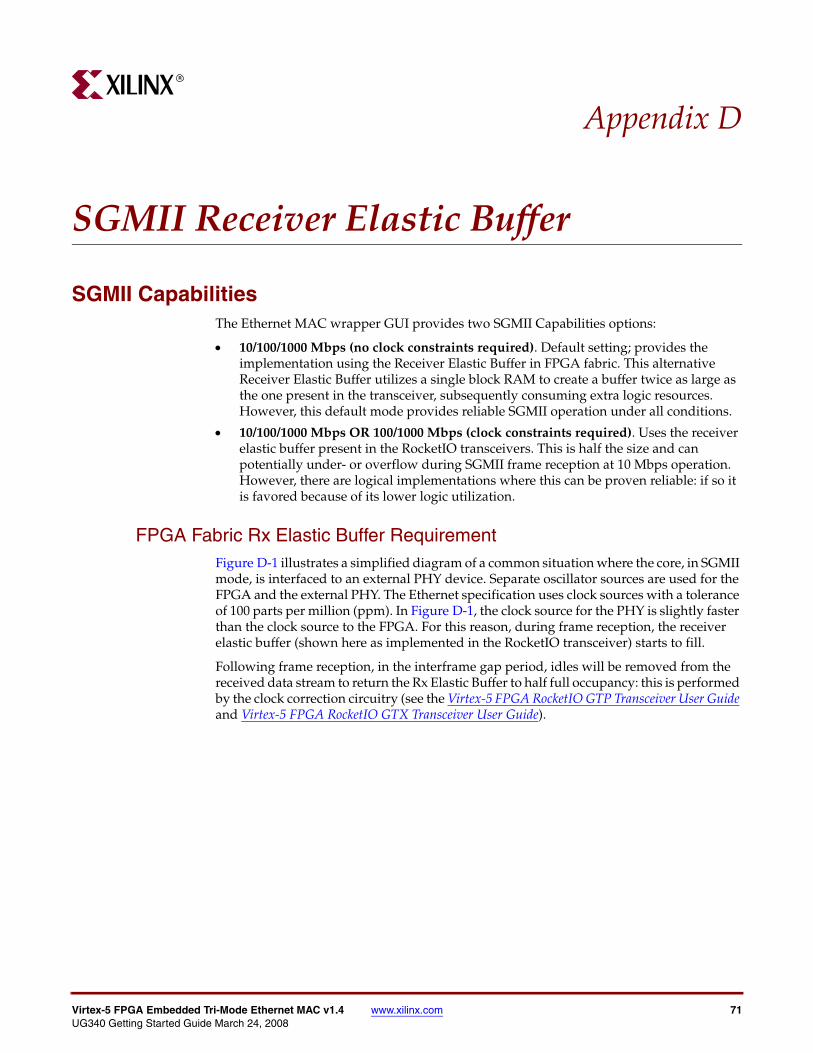
Virtex-5 FPGA Embedded Tri-Mode Ethernet MAC v1.4 www.xilinx.com 71UG340 Getting Started Guide March 24, 2008
R
Appendix D
SGMII Receiver Elastic Buffer
SGMII CapabilitiesThe Ethernet MAC wrapper GUI provides two SGMII Capabilities options:
• 10/100/1000 Mbps (no clock constraints required). Default setting; provides the implementation using the Receiver Elastic Buffer in FPGA fabric. This alternative Receiver Elastic Buffer utilizes a single block RAM to create a buffer twice as large as the one present in the transceiver, subsequently consuming extra logic resources. However, this default mode provides reliable SGMII operation under all conditions.
• 10/100/1000 Mbps OR 100/1000 Mbps (clock constraints required). Uses the receiver elastic buffer present in the RocketIO transceivers. This is half the size and can potentially under- or overflow during SGMII frame reception at 10 Mbps operation. However, there are logical implementations where this can be proven reliable: if so it is favored because of its lower logic utilization.
FPGA Fabric Rx Elastic Buffer RequirementFigure D-1 illustrates a simplified diagram of a common situation where the core, in SGMII mode, is interfaced to an external PHY device. Separate oscillator sources are used for the FPGA and the external PHY. The Ethernet specification uses clock sources with a tolerance of 100 parts per million (ppm). In Figure D-1, the clock source for the PHY is slightly faster than the clock source to the FPGA. For this reason, during frame reception, the receiver elastic buffer (shown here as implemented in the RocketIO transceiver) starts to fill.
Following frame reception, in the interframe gap period, idles will be removed from the received data stream to return the Rx Elastic Buffer to half full occupancy: this is performed by the clock correction circuitry (see the Virtex-5 FPGA RocketIO GTP Transceiver User Guide and Virtex-5 FPGA RocketIO GTX Transceiver User Guide).

72 www.xilinx.com Virtex-5 FPGA Embedded Tri-Mode Ethernet MAC v1.4UG340 Getting Started Guide March 24, 2008
Appendix D: SGMII Receiver Elastic BufferR
Analysis
Assuming separate clock sources, each with a tolerance of 100 ppm, the maximum frequency difference between the two devices can be 200 ppm. It can be shown that this translates into a full clock period difference every 5000 clock periods.
Relating this to an Ethernet frame, a single byte of difference every 5000 bytes of received frame data occurs, causing the Rx Elastic Buffer to either fill or empty by an occupancy of one.
The maximum sized Ethernet frame (non-jumbo) is of size 1522 bytes for a VLAN frame:
• At 1 Gbps operation, this translates into 1522 clock cycles
• At 100 Mbps operation, this translates into 15220 clock cycles (since each byte is repeated 10 times
• At 10 Mbps operation, this translates into 152200 clock cycles (since each byte is repeated 100 times).
Considering the 10 Mbps case, we would need 152200/5000 = 31 FIFO entries in the Elastic Buffer above and below the half way point to guarantee that the buffer will not under or overflow during frame reception. This assumes that frame reception begins when the buffer is exactly half full.
The size of the Rx Elastic Buffer in the RocketIOs is of size 64 entries. However, we cannot assume that the buffer is exactly half-full at the start of frame reception. Additionally, the underflow and overflow thresholds are not exact. See the RocketIO User Guides, available from www.xilinx.com:
• Virtex-5 FPGA RocketIO GTP Transceiver User Guide (UG196)
• Virtex-5 FPGA RocketIO GTX Transceiver User Guide (UG198)
Figure D-1: SGMII Implementation: Separate Clock Sources
RxElasticBuffer
TXP/TXN
RXP/RXN
SGMII Link
10 BASE-T
100BASE-T
1000BASE-T
PHY
FPGA
125 MHz -100 ppm 125 MHz + 100ppm
Virtex-5 Embedded Tri-Mode Ethernet
MAC Wrapper
RocketIO
Transceiver
Twisted
Copper
Pair

Virtex-5 FPGA Embedded Tri-Mode Ethernet MAC v1.4 www.xilinx.com 73UG340 Getting Started Guide March 24, 2008
SGMII CapabilitiesR
To guarantee reliable SGMII operation at 10 Mbps (non-jumbo frames), the RocketIO Elastic Buffer must be bypassed and a larger buffer implemented in the FPGA fabric. The fabric buffer, provided by the example design, is twice the size and so nominally provides 64 entries above and below the half full threshold. This has been proven to cope with standard (non-jumbo) Ethernet frames at all three SGMII speeds.
The RocketIO Rx Elastic BufferThe Elastic Buffer in the RocketIO can be used reliably under the following conditions:
• When 10 Mbps operation is not required (for example, when connecting the core to the 1-Gigabit Ethernet MAC to provide only 1 Gbps operation). Please note that both 1 Gbps and 100 Mbps operation are guaranteed.
• When the clocks are closely related (see below).
If any uncertainty exists, select the FPGA fabric Rx Elastic Buffer Implementation.
Closely Related Clock Sources
Scenario 1
Figure D-2 illustrates a simplified diagram of a common situation where the core, in SGMII mode, is interfaced to an external PHY device. Note that a common oscillator source is used for both the FPGA and the external PHY.
If the PHY device sources the receiver SGMII stream synchronously from the shared oscillator (check PHY data sheet), then the RocketIO will receive data at exactly the same rate as that used by the core: the receiver elastic buffer will neither empty nor fill, having the same frequency clock on either side.
In this situation, the receiver elastic buffer will not under or overflow and the elastic buffer implementation in the RocketIO should be used to save logic resources.
Figure D-2: SGMII Implementation: Shared Clock Sources
RxElasticBuffer
TXP/TXN
RXP/RXN
SGMII Link
10 BASE-T
100BASE-T
1000BASE-T
PHY
FPGA
125MHz -100ppm
Virtex-5 Embedded Tri-Mode Ethernet
MAC Wrapper
RocketIO
Transceiver
Twisted
Copper
Pair

74 www.xilinx.com Virtex-5 FPGA Embedded Tri-Mode Ethernet MAC v1.4UG340 Getting Started Guide March 24, 2008
Appendix D: SGMII Receiver Elastic BufferR
Scenario 2
Now consider again the case illustrated by Figure D-1. However, this time, assume that the clock sources used are both 50 ppm. Now the maximum frequency difference between the two devices is 100 ppm. It can be shown that this translates into a full clock period difference every 10000 clock periods, resulting in a requirement for 16 FIFO entries above and below the half-full point. It can be demonstrated that this provides reliable operation with the RocketIO Rx Elastic Buffers. Again, see the PHY data sheet to ensure that the PHY device sources the receiver SGMII stream synchronously to its reference oscillator.
Jumbo Frame ReceptionA jumbo frame is an Ethernet frame that is deliberately larger than the maximum-size Ethernet frame allowed in the IEEE802.3 specification. Jumbo frames require special consideration to reliably receive frames. Table D-1 defines the maximum-size jumbo frames that can be received reliably when using the Receiver Elastic Buffer.
Table D-1: Maximum Frame Sizes for Fabric Rx Elastic Buffers (100 ppm Clock Tolerance)
Standard/Speed Maximum Frame Size
1000BASE-X (1 Gbps only) 280000
SGMII (1 Gbps) 280000
SGMII (100 Mbps) 28000
SGMII (10 Mbps) 2800