viii. simple cmos operational amplifiers (op …nicoskun/allan_hollberg_opamp_design.pdf ·...
TRANSCRIPT
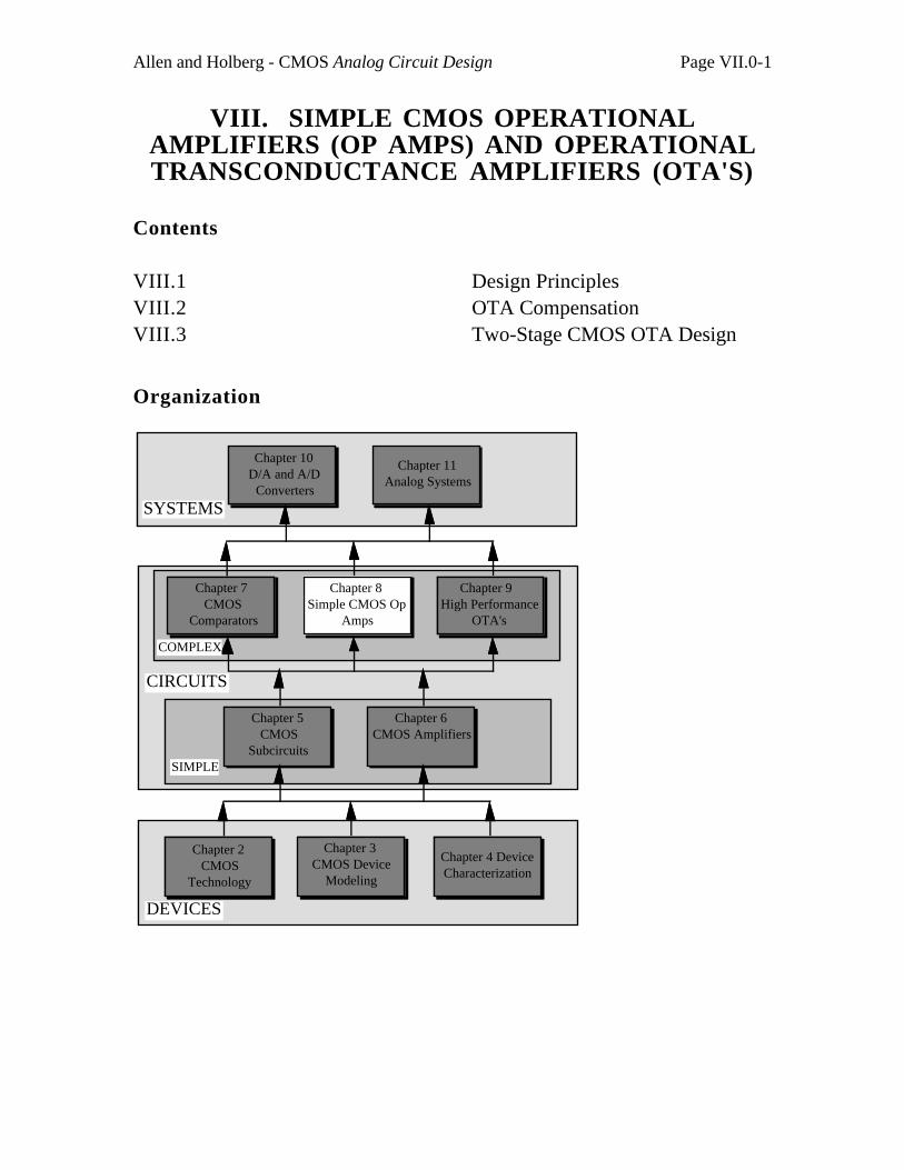
Allen and Holberg - CMOS Analog Circuit Design Page VII.0-1
VIII. SIMPLE CMOS OPERATIONALAMPLIFIERS (OP AMPS) AND OPERATIONALTRANSCONDUCTANCE AMPLIFIERS (OTA'S)
Contents
VIII.1 Design PrinciplesVIII.2 OTA CompensationVIII.3 Two-Stage CMOS OTA Design
Organization
DEVICES
SYSTEMS
CIRCUITS
Chapter 2 CMOS
Technology
Chapter 3 CMOS Device
Modeling
Chapter 4 Device Characterization
Chapter 7 CMOS
Comparators
Chapter 8 Simple CMOS Op
Amps
Chapter 9 High Performance
OTA's
Chapter 5 CMOS
Subcircuits
Chapter 6 CMOS Amplifiers
Chapter 10D/A and A/D
Converters
Chapter 11Analog Systems
SIMPLE
COMPLEX
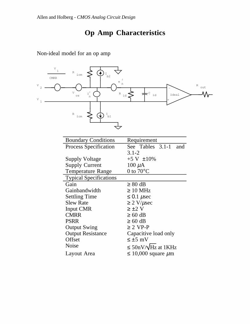
Allen and Holberg - CMOS Analog Circuit Design
Op Amp Characteristics
Non-ideal model for an op amp
b1I
b2I
Ricm
Ricm
CMRR
V1
CidR
idV1
V2
Ideal
+
-R
out
en
2
nI2V
os
Boundary Conditions RequirementProcess Specification See Tables 3.1-1 and
3.1-2Supply Voltage +5 V ±10%Supply Current 100 µATemperature Range 0 to 70°CTypical SpecificationsGain ≥ 80 dBGainbandwidth ≥ 10 MHzSettling Time ≤ 0.1 µsecSlew Rate ≥ 2 V/µsecInput CMR ≥ ±2 VCMRR ≥ 60 dBPSRR ≥ 60 dBOutput Swing ≥ 2 VP-POutput Resistance Capacitive load onlyOffset ≤ ±5 mVNoise ≤ 50nV/ Hz at 1KHzLayout Area ≤ 10,000 square µm
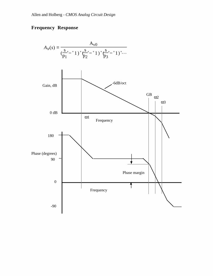
Allen and Holberg - CMOS Analog Circuit Design
Frequency Response
Av(s) = Av0
(s
p1 − 1 ) (
sp2
− 1 ) (s
p3 − 1) . . .
Gain, dB
Phase (degrees)
180
90
0
-6dB/oct
GBω2
ω3
ω1Frequency
Frequency
Phase margin
0 dB
-90
Allen and Holberg - CMOS Analog Circuit Design
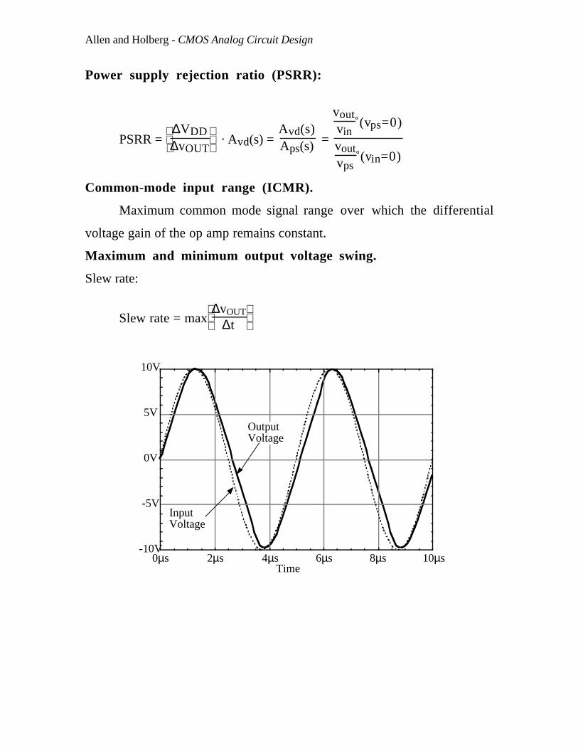
Power supply rejection ratio (PSRR):
PSRR =
∆VDD
∆vOUT · Avd(s) =
Avd(s)Aps(s) =
voutvin
(vps=0)
voutvps
(vin=0)
Common-mode input range (ICMR).
Maximum common mode signal range over which the differential
voltage gain of the op amp remains constant.
Maximum and minimum output voltage swing.
Slew rate:
Slew rate = max
∆vOUT
∆t
-10V
-5V
0V
5V
10V
0µs 2µs 4µs 6µs 8µs 10µs
InputVoltage
OutputVoltage
Time
Allen and Holberg - CMOS Analog Circuit Design
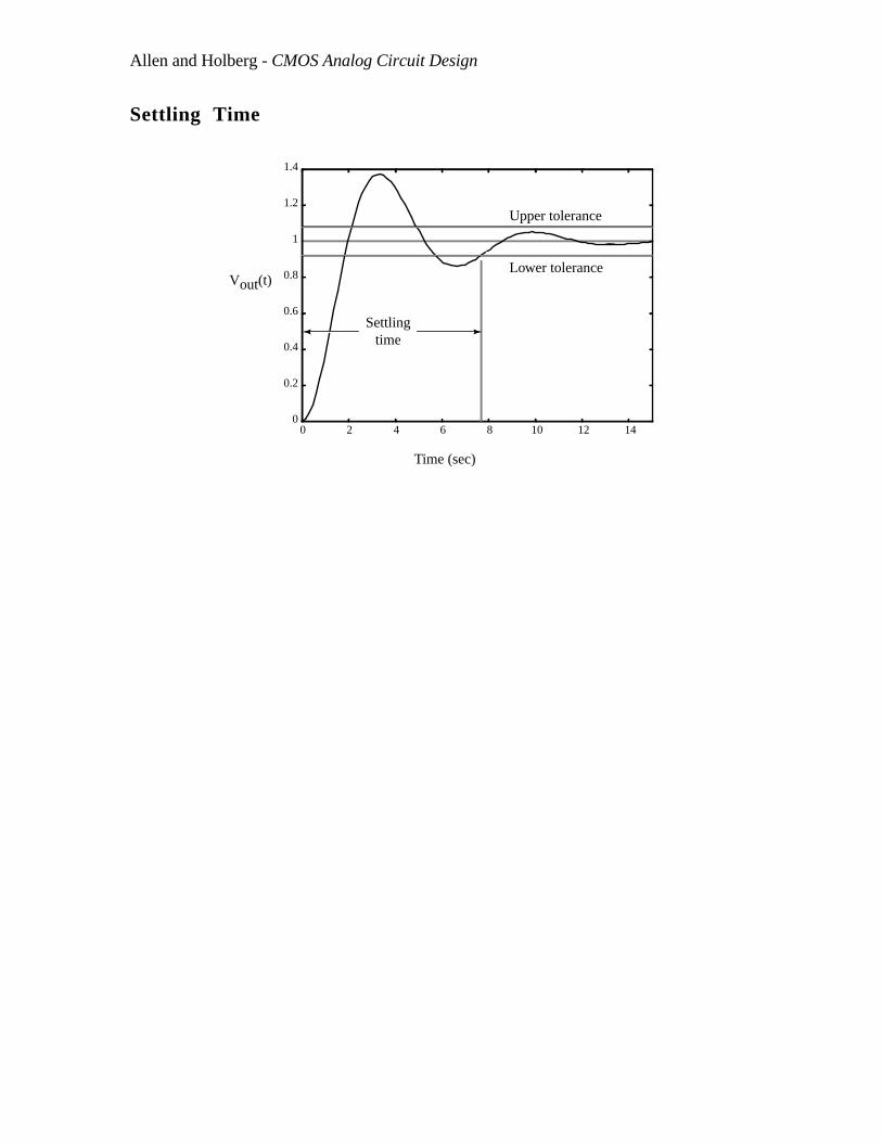
Settling Time
0
0.2
0.4
0.6
0.8
1
1.2
1.4
0 2 4 6 8 10 12 14
Lower tolerance
Upper tolerance
Settling time
Time (sec)
Vout(t)

Allen and Holberg - CMOS Analog Circuit Design
Design Approach
SpecificationsAnalysis
Simulation
Modify
Design
Iterate
Specifications:
• Gain • Bandwidth
• Output voltage swing • PSRR
• Settling time • CMRR
• Power dissipation • Noise
• Supply voltage • Common-mode input range
• Silicon area

Allen and Holberg - CMOS Analog Circuit Design
Design Strategy
The design process involves two distinct activities:
Architecture Design
• Find an architecture already available and adapt it to present
requirements
• Create a new architecture that can meet requirements
Component Design
• Design transistor sizes
• Design compensation network
If available architectures do not meet requirements, then an existing
architecture must be modified, or a new one designed. Once a satisfactory
architecture has been obtained, then devices and the compensation network
must be designed.

Allen and Holberg - CMOS Analog Circuit Design
Op Amp Architecture
M4M3
M1
+-M2
M5
M6
M7
IBias
VDD
vOUTCompensation

Allen and Holberg - CMOS Analog Circuit Design
Compensation
In virtually all op amp applications, feedback will be applied around the
amplifier. Therefore, stable performance requires that the amplifier be
compensated. Essentially we desire that the loop gain be less than unity
when the phase shift around the loop is greater than 135˚
Σ
β
A+
-
OUTIN
OUT
IN
A
A=
+1 β
Goal: 1 + Aβ > 0
Rule of thumb: arg[Aβ] < 135˚ at mag[Aβ] = 1

Allen and Holberg - CMOS Analog Circuit Design
Graphical Illustration of Stability Requirements
|Aβ| (dB)
180o
90o
0o
-6dB/oct
GB
ω2ω1Frequency
Frequency
-12dB/oct
Arg[Aβ]
β=1
0 dB
Allen and Holberg - CMOS Analog Circuit Design
Step Response of Two-Pole SystemImpact of placing ω2 at different locations:
0s 5us 10us 15us 20us
Timev(5)
1.5V
1.0V
0.5V
0V
stabilityDate/Time run: 04/08/97 19:45:36 Temperature: 27.0
ω1 = 1000 rps
Case 1: ω2 = 1 x 10⁶ rps
Case 2: ω2 = 0.5 x 10⁶ rps
Case 3: ω2 = 0.25 x 10⁶ rps
1
2
3

Allen and Holberg - CMOS Analog Circuit Design
Types of Compensation
1. Miller - Use of a capacitor feeding back around a high-gain, inverting
stage.
• Miller capacitor only
• Miller capacitor with an unity-gain buffer to block the forward
path through the compensation capacitor. Can eliminate the RHP
zero.
• Miller with a nulling resistor. Similar to Miller but with an added
series resistance to gain control over the RHP zero.
2. Self compensating - Load capacitor compensates the op amp (later).
3. Feedforward - Bypassing a positive gain amplifier resulting in phase
lead. Gain can be less than unity.

Allen and Holberg - CMOS Analog Circuit Design
Miller Compensation
M4M3
M1
+-M2
M5
M6
M7
IBias
VDD
vOUT
C1CL
CM Cc
Small-signal model
+
- -
+
CLC1
Cc
CMgm1 v1
gm3gm2
vin2
-vin2 rds1
1
gm4v1
v2
gds2+gds4
1
gm6v2
gds6+gds71
-
+
vout
Simplified small-signal model
-
+
CLC1
Cc
gm1vinv2
gds2+gds4
1
gm6v2
gds6+gds7
1
-
+
voutvin
-
+

Allen and Holberg - CMOS Analog Circuit Design
Analysis
Vo(s)
Vin(s) = (gmI)(gmII)(RI)(RII)(1 - sCc/gmII)
1 + s[RI(C1 + Cc) + RII(CL + Cc) + gmIIRIRIICc] + s2RIRII[C1CL + Cc(C1+ CL)]
p1 ≅ -1
gmII RI RII Cc
p2 ≅ -gmIICc
C1CL + CLCc + C1Cc
p2 ≅ -gmIICL
z1 = gmIICc
wheregmI = gm1 = gm2 gmII = gm6
RI = 1
gds2+gds4RII =
1gds6+gds7

Allen and Holberg - CMOS Analog Circuit Design
Miller Compensation
Phase margin
180o
90o
0o
-6dB/oct
GB
ω2ω1Frequency
Frequency
-12dB/oct
Arg[Aβ]
β=1
Before compensation
After compensation
Before compensation
After compensation
|Aβ| (dB)

Allen and Holberg - CMOS Analog Circuit Design
Conditions for Stability
• Unity-gainbandwith is given as:
GB = Av(0)·|p1| = ( )gmIgmIIRIRII ·
1
gmIIRIRIICc =
gmICc
• The requirement for 45° phase margin is:
Arg[Aß] = ±180° - tan-1
ω
|p1| - tan-1
ω
|p2| - tan-1
ω
z = 45°
Let ω = GB and assume that z ≥ 10GB, therefore we get,
±180° - tan-1
GB
|p1| - tan-1
GB
|p2| - tan-1
GB
z = 45°
or
135° ≈ tan-1(Av(0)) + tan-1
GB
|p2| + tan-1(0.1) = 90° + tan-1
GB
|p2 | + 5.7°
39.3° ≈ tan-1
GB
|p2| ⇒ GB|p2| = 0.818 ⇒ |p2| ≥ 1.22GB
• The requirement for 60° phase margin:
| p2 | ≥ 2.2GB if z ≥ 10GB

Allen and Holberg - CMOS Analog Circuit Design
• If 60° phase margin is required, then the following relationships apply:
gmIICc
> 10gmI
Cc ⇒ gm II > 10gm I
Furthermore,gmIIC2
> 2.2gmI
Cc
which after substitution gives:
Cc > 0.22C2
Note:gmI = gm1 = gm2 and gmII = gm6

Allen and Holberg - CMOS Analog Circuit Design
Phase margin = 45 degreesPhase margin = 60 degrees
Parasitic pole, ω2, held constantwhile dominant pole, ω1, is moved.
Allen and Holberg - CMOS Analog Circuit Design
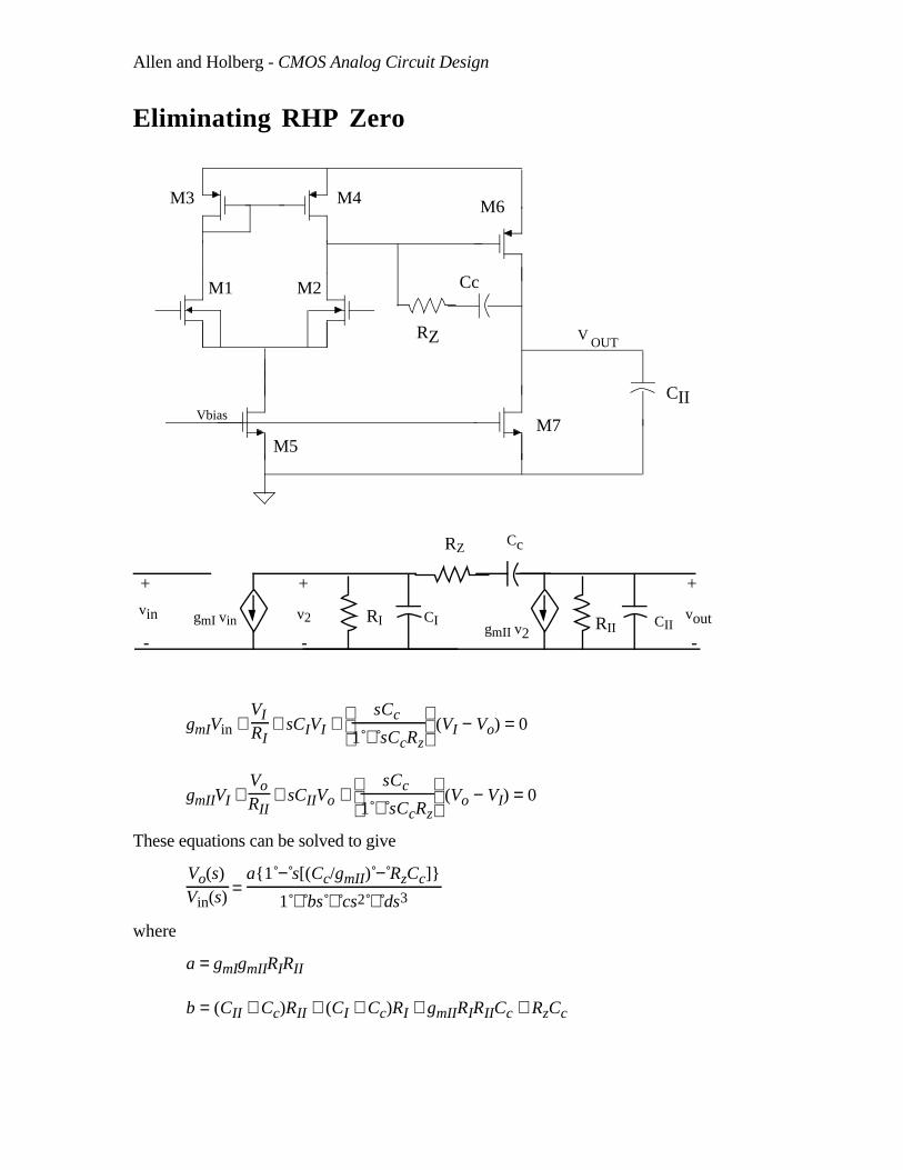
Eliminating RHP Zero
V OUT
M7
M1 M2
M3 M4
M5
M6
Vbias
Cc
CII
-
+
CIICI
Cc
gmI vin v2gmII v2
-
+
voutvin
-
+
RI RII
RZ
RZ
gmIVin + VIRI
+ sCIVI +
sCc
1 + sCcRz (VI − Vo) = 0
gmIIVI + VoRII
+ sCIIVo +
sCc
1 + sCcRz (Vo − VI) = 0
These equations can be solved to give
Vo(s)Vin(s) =
a{1 − s[(Cc/gmII) − RzCc]}
1 + bs + cs2 + ds3
where
a = gmIgmIIRIRII
b = (CII + Cc)RII + (CI + Cc)RI + gmIIRIRIICc + RzCc

Allen and Holberg - CMOS Analog Circuit Design
c = [RIRII(CICII + CcCI + CcCII) + RzCc(RICI + RIICII)]
d = RIRIIRzCICIICc
If Rz is assumed to be less than RI or RII and the poles widely spaced, then the roots are
p1 ≅ −1
(1 + gmIIRII)RICc ≅
−1gmIIRIIRICc
p2 ≅ −gmIICc
CICII + CcCI + CcCII ≅
−gmIICII
p3 = −1
RzCI
and
z1 = 1
Cc(1/gmII − Rz)
By setting
Rz = 1/gmII
The RHP zero moves to infinity
Allen and Holberg - CMOS Analog Circuit Design
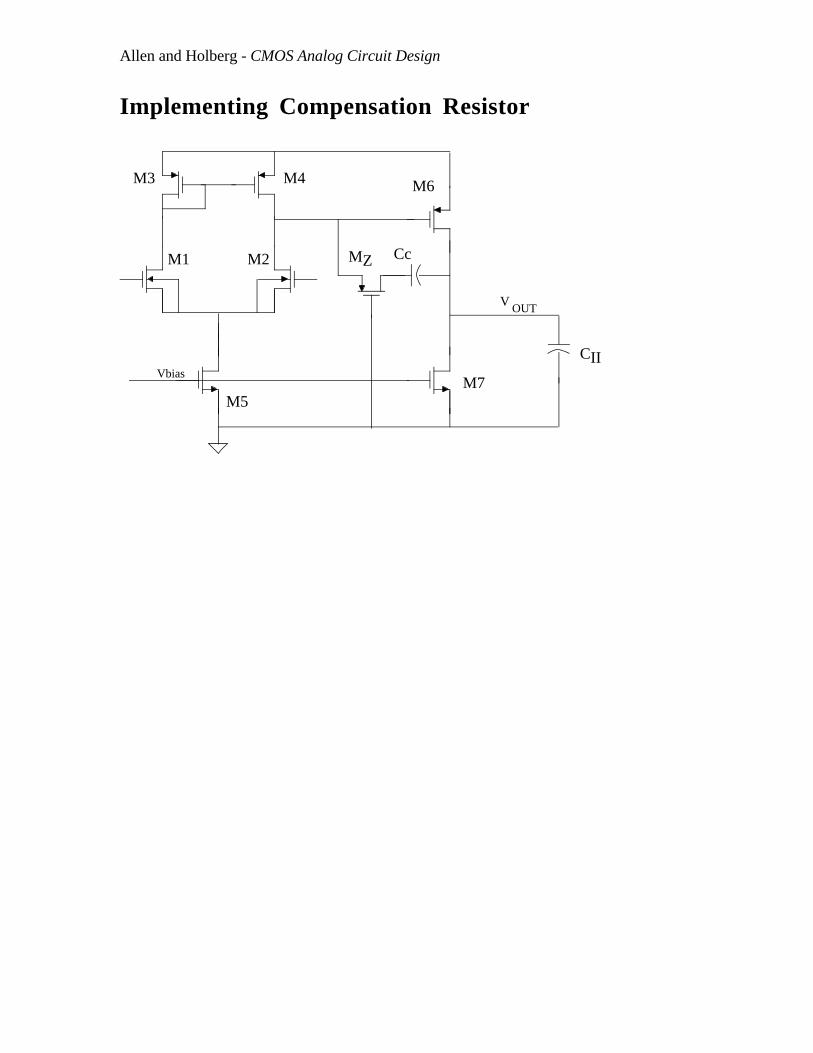
Implementing Compensation Resistor
V OUT
M7
M1 M2
M3 M4
M5
M6
Vbias
Cc
CII
MZ

Allen and Holberg - CMOS Analog Circuit Design
Two-Stage Operational Amplifier Design
-
+
vin
M1 M2
M3 M4
M5
M6
M7
vout
VDD
VSS
VBias+
-
Cc
CL
Figure 6.3-1 Schematic of an unbuffered, two-stage CMOS op amp with an n-channel input pair.Important relationships:
gm1 = gm2 = gmI, gm6 = gmII, gds2 + gds4 = GI, and gds6 + gds7 = GII.
Slew rate SR = I5Cc
(1)
First-stage gain Av1 = gm1
gds2 + gds4 =
2gm1
I5(λ2 + λ4)(2)
Second-stage gain Av2 = gm6
gds6 + gds7 =
gm6
I6(λ6 + λ7)(3)
Gain-bandwidth GB = gm1Cc
(4)
Output pole p2 = −gm6CL
(5)
RHP zero z1 = gm6Cc
(6)
Positive CMR Vin(max) = VDD − I5
β3 − |VT03|(max) + VT1(min)) (7)

Allen and Holberg - CMOS Analog Circuit Design
Negative CMR Vin(min) = VSS + I5
β1 + VT1(max) + VDS5(sat) (8)
Saturation voltageVDS(sat) = 2IDS
β(9)
All transistors are in saturation for the above relationships.
The following design procedure assumes that specifications for the following parametersare given.
1. Gain at dc, Av(0)2. Gain-bandwidth, GB3. Input common-mode range, ICMR4. Load Capacitance, CL5. Slew-rate, SR6. Output voltage swing7. Power dissipation, Pdiss
Choose a device length to establish of the channel-length modulation parameter λ.
Design the compensation capacitor Cc. It was shown that placing the loading pole p2 2.2
times higher than the GB permitted a 60° phase margin (assuming that the RHP zero z1 isplaced at or beyond ten times GB). This results in the following requirement for theminimum value for Cc.
Cc > (2.2/10)CL
Next, determine the minimum value for the tail current I5, based upon slew-raterequirements. Using Eq. (1), the value for I5 is determined to be
I5 = SR (Cc)
If the slew-rate specification is not given, then one can choose a value based upon settling-time requirements. Determine a value that is roughly ten times faster than the settling-timespecification, assuming that the output slews approximately one-half of the supply rail. Thevalue of I5 resulting from this calculation can be changed later if need be.
The aspect ratio of M3 can now be determined by using the requirement for positive inputcommon-mode range. The following design equation for (W/L)3 was derived fromEq. (7).
S3 = (W/L)3 = I5
(K'3) [VDD − Vin(max) − |VT03|(max) + VT1(min)]2
If the value determined for (W/L)3 is less than one, then it should be increased to a valuethat minimizes the product of W and L. This minimizes the area of the gate region, which
Allen and Holberg - CMOS Analog Circuit Design
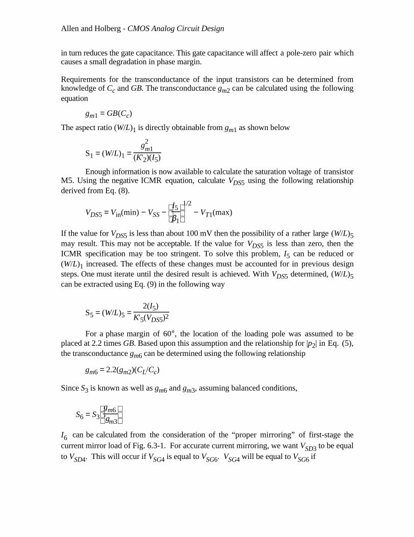
in turn reduces the gate capacitance. This gate capacitance will affect a pole-zero pair whichcauses a small degradation in phase margin.
Requirements for the transconductance of the input transistors can be determined fromknowledge of Cc and GB. The transconductance gm2 can be calculated using the followingequation
gm1 = GB(Cc)
The aspect ratio (W/L)1 is directly obtainable from gm1 as shown below
S1 = (W/L)1 = g2
m1(K'2)(I5)
Enough information is now available to calculate the saturation voltage of transistorM5. Using the negative ICMR equation, calculate VDS5 using the following relationshipderived from Eq. (8).
VDS5 = Vin(min) − VSS −
I5
β1
1/2
− VT1(max)
If the value for VDS5 is less than about 100 mV then the possibility of a rather large (W/L)5may result. This may not be acceptable. If the value for VDS5 is less than zero, then theICMR specification may be too stringent. To solve this problem, I5 can be reduced or(W/L)1 increased. The effects of these changes must be accounted for in previous designsteps. One must iterate until the desired result is achieved. With VDS5 determined, (W/L)5can be extracted using Eq. (9) in the following way
S5 = (W/L)5 = 2(I5)
K'5(VDS5)2
For a phase margin of 60°, the location of the loading pole was assumed to beplaced at 2.2 times GB. Based upon this assumption and the relationship for |p2| in Eq. (5),the transconductance gm6 can be determined using the following relationship
gm6 = 2.2(gm2)(CL/Cc)
Since S3 is known as well as gm6 and gm3, assuming balanced conditions,
S6 = S3
gm6
gm3
I6 can be calculated from the consideration of the “proper mirroring” of first-stage thecurrent mirror load of Fig. 6.3-1. For accurate current mirroring, we want VSD3 to be equalto VSD4. This will occur if VSG4 is equal to VSG6. VSG4 will be equal to VSG6 if
Allen and Holberg - CMOS Analog Circuit Design
I6 = (W/L)6(W/L)4
I1 =
S6
S4 I1
Choose the larger of these two values for I6 (Eq. 19 or Eq. 20). If the larger value is foundin Eq (19), then (W/L)6 must be increased to satisfy Eq. (20). If the larger value is found inEq. (20), then no other adjustments must be made. One also should check the powerdissipation requirements since I6 will most likely determine the majority of the powerdissipation.
The device size of M7 can be determined from the balance equation given below
S7 = (W/L)7 = (W/L)5
I6
I5 = S5
I6
I5
The first-cut design of all W/L ratios are now complete. Fig. 6.3-2 illustrates the abovedesign procedure showing the various design relationships and where they apply in thetwo-stage CMOS op amp.
-
+
vin M1 M2
M3 M4
M5
M6
M7
vout
VDD
VSS
VBias+
-
Cc
CL
VSG4+
-
Max. ICMRand/or p3
VSG6+
-
Vout(max)
I6
gm6 or Proper Mirroring
VSG4=VSG6
Cc ≈ 0.2CL(PM = 60°)
GB =gm1Cc
Min. ICMR I5 I5 = SR·Cc Vout(min)
Figure 6.3-2 Illustration of the design relationships and the circuit fora two-stage CMOS op amp.
At this point in the design procedure, the total amplifier gain must be checked against thespecifications.
Av = (2)(gm2)(gm6)
I5(λ2 + λ3)I6(λ6 + λ7)
If the gain is too low, a number of things can be adjusted. The best way to do this is to usethe table below, which shows the effects of various device sizes and currents on the
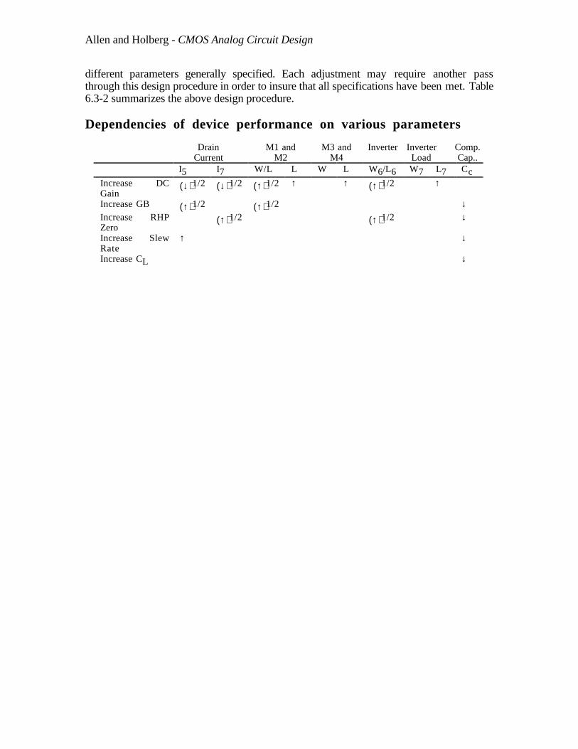
Allen and Holberg - CMOS Analog Circuit Design
different parameters generally specified. Each adjustment may require another passthrough this design procedure in order to insure that all specifications have been met. Table6.3-2 summarizes the above design procedure.
Dependencies of device performance on various parameters
Drain M1 and M3 and Inverter Inverter Comp.Current M2 M4 Load Cap..
I5 I7 W/L L W L W6/L6 W7 L7 CcIncrease DCGain
(↓)1/2 (↓)1/2 (↑)1/2 ↑ ↑ (↑)1/2 ↑
Increase GB (↑)1/2 (↑)1/2 ↓Increase RHPZero
(↑)1/2 (↑)1/2 ↓
Increase SlewRate
↑ ↓
Increase CL ↓
Allen and Holberg - CMOS Analog Circuit Design
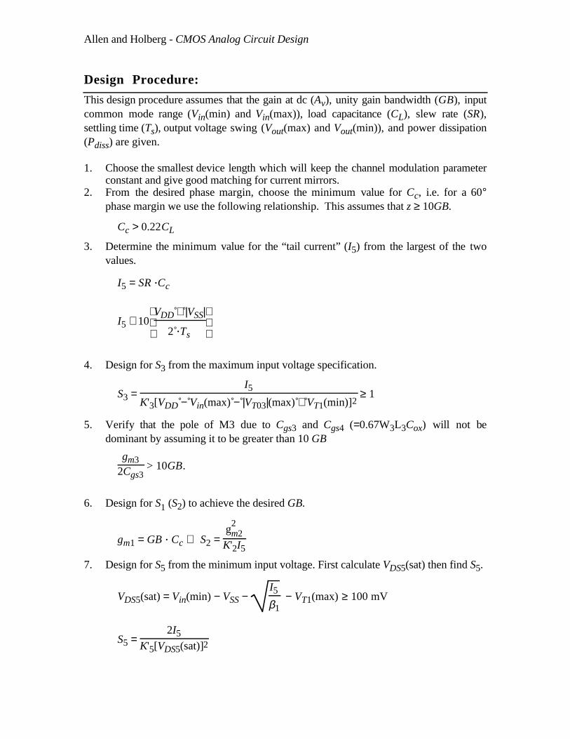
Design Procedure:
This design procedure assumes that the gain at dc (Av), unity gain bandwidth (GB), inputcommon mode range (Vin(min) and Vin(max)), load capacitance (CL), slew rate (SR),settling time (Ts), output voltage swing (Vout(max) and Vout(min)), and power dissipation(Pdiss) are given.
1. Choose the smallest device length which will keep the channel modulation parameterconstant and give good matching for current mirrors.
2. From the desired phase margin, choose the minimum value for Cc, i.e. for a 60°phase margin we use the following relationship. This assumes that z ≥ 10GB.
Cc > 0.22CL
3. Determine the minimum value for the “tail current” (I5) from the largest of the twovalues.
I5 = SR .Cc
I5 ≅ 10
VDD + |VSS|
2 .Ts
4. Design for S3 from the maximum input voltage specification.
S3 = I5
K'3[VDD − Vin(max) − |VT03|(max) + VT1(min)]2 ≥ 1
5. Verify that the pole of M3 due to Cgs3 and Cgs4 (=0.67W3L3Cox) will not bedominant by assuming it to be greater than 10 GB
gm32Cgs3
> 10GB.
6. Design for S1 (S2) to achieve the desired GB.
gm1 = GB . Cc ⇒ S2 = g
2m2
K'2I5
7. Design for S5 from the minimum input voltage. First calculate VDS5(sat) then find S5.
VDS5(sat) = Vin(min) − VSS − I5
β1 − VT1(max) ≥ 100 mV
S5 = 2I5
K'5[VDS5(sat)]2

Allen and Holberg - CMOS Analog Circuit Design
8. Find gm6 and S6 by the relationship relating to phase margin, load, and compensationcapacitors, and the balance condition.
gm6 = 2.2gm2(CL/Cc)
S6 = S3
gm6
gm3
9. Calculate I6 :
I6 = (S6/S4)I4 = (S6/S4)(I5/2)
10. Design S7 to achieve the desired current ratios between I5 and I6.
S7 = (I6/I5)S5
11. Check gain and power dissipation specifications.
Av = 2gm2gm6
I5(λ2 + λ3)I6(λ6 + λ7)
Pdiss = (I5 + I6)(VDD + |VSS|)
12. If the gain specification is not met, then the currents, I5 and I6, can be decreased or theW/L ratios of M2 and/or M6 increased. The previous calculations must be recheckedto insure that they have been satisfied. If the power dissipation is too high, then onecan only reduce the currents I5 and I6. Reduction of currents will probably necessitateincrease of some of the W/L ratios in order to satisfy input and output swings.
13. Simulate the circuit to check to see that all specifications are met.
Allen and Holberg - CMOS Analog Circuit Design
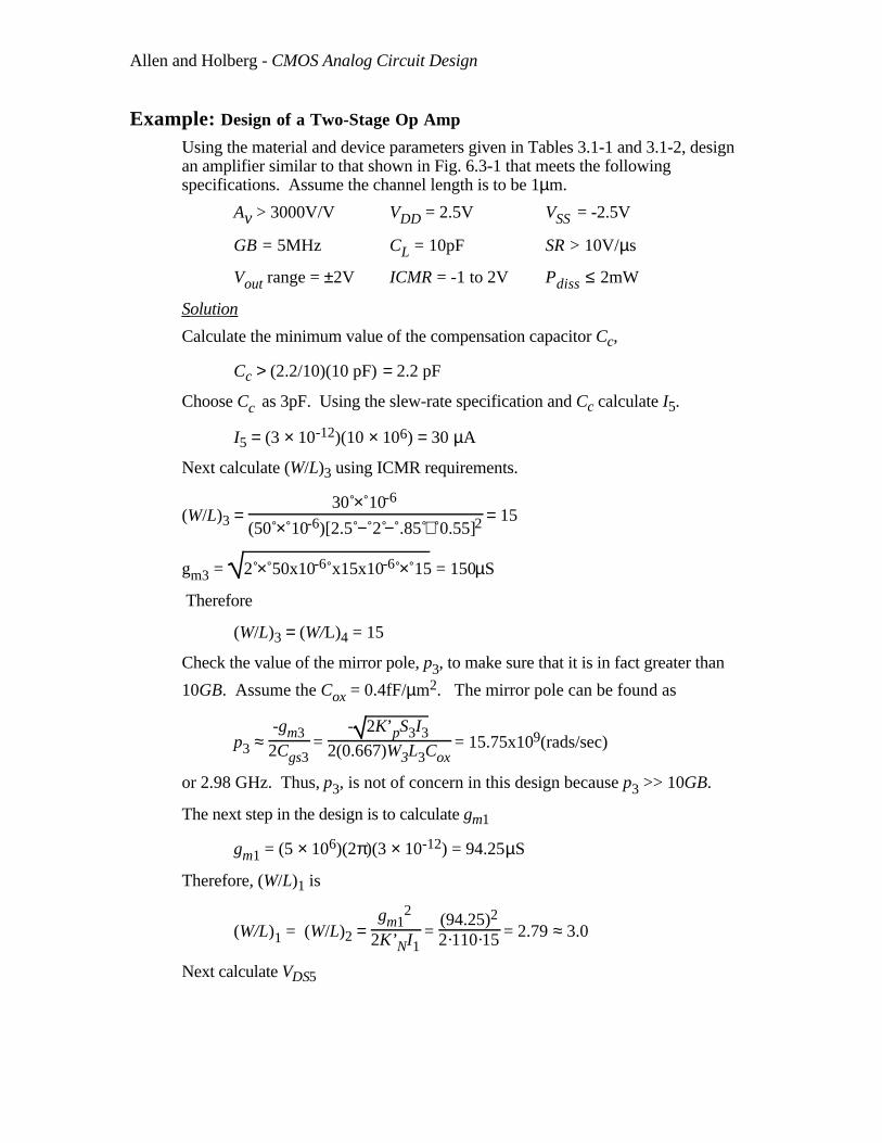
Example: Design of a Two-Stage Op Amp
Using the material and device parameters given in Tables 3.1-1 and 3.1-2, designan amplifier similar to that shown in Fig. 6.3-1 that meets the followingspecifications. Assume the channel length is to be 1µm.
Av > 3000V/V VDD = 2.5V VSS = -2.5V
GB = 5MHz CL = 10pF SR > 10V/µs
Vout range = ±2V ICMR = -1 to 2V Pdiss ≤ 2mW
Solution
Calculate the minimum value of the compensation capacitor Cc,
Cc > (2.2/10)(10 pF) = 2.2 pF
Choose Cc as 3pF. Using the slew-rate specification and Cc calculate I5.
I5 = (3 × 10-12)(10 × 106) = 30 µA
Next calculate (W/L)3 using ICMR requirements.
(W/L)3 = 30 × 10-6
(50 × 10-6)[2.5 − 2 − .85 + 0.55]2 = 15
gm3 = 2 × 50x10-6 x15x10-6 × 15 = 150µS
Therefore
(W/L)3 = (W/L)4 = 15
Check the value of the mirror pole, p3, to make sure that it is in fact greater than
10GB. Assume the Cox = 0.4fF/µm2. The mirror pole can be found as
p3 ≈ -gm32Cgs3
= - 2K’pS3I3
2(0.667)W3L3Cox = 15.75x10⁹(rads/sec)
or 2.98 GHz. Thus, p3, is not of concern in this design because p3 >> 10GB.
The next step in the design is to calculate gm1
gm1 = (5 × 10⁶)(2π)(3 × 10-12) = 94.25µS
Therefore, (W/L)1 is
(W/L)1 = (W/L)2 = gm1
2
2K’NI1 =
(94.25)2
2·110·15 = 2.79 ≈ 3.0
Next calculate VDS5
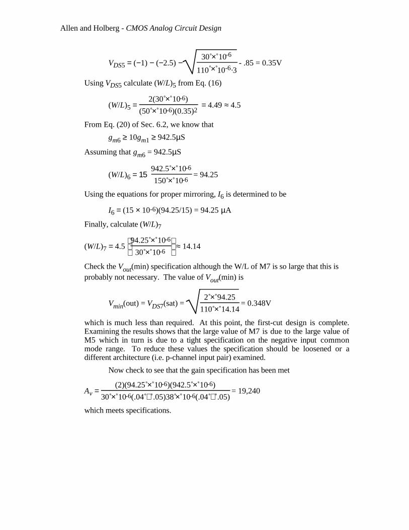
Allen and Holberg - CMOS Analog Circuit Design
VDS5 = (−1) − (−2.5) −30 × 10-6
110 × 10-6·3 - .85 = 0.35V
Using VDS5 calculate (W/L)5 from Eq. (16)
(W/L)5 = 2(30 × 10-6)
(50 × 10-6)(0.35)2 = 4.49 ≈ 4.5
From Eq. (20) of Sec. 6.2, we know that
gm6 ≥ 10gm1 ≥ 942.5µS
Assuming that gm6 = 942.5µS
(W/L)6 = 15 942.5 × 10⁻⁶
150 × 10-6 = 94.25
Using the equations for proper mirroring, I6 is determined to be
I6 = (15 × 10-6)(94.25/15) = 94.25 µA
Finally, calculate (W/L)7
(W/L)7 = 4.5
94.25 × 10⁻⁶
30 × 10-6 ≈ 14.14
Check the Vout(min) specification although the W/L of M7 is so large that this isprobably not necessary. The value of Vout(min) is
Vmin(out) = VDS7(sat) = 2 × 94.25
110 × 14.14 = 0.348V
which is much less than required. At this point, the first-cut design is complete.Examining the results shows that the large value of M7 is due to the large value ofM5 which in turn is due to a tight specification on the negative input commonmode range. To reduce these values the specification should be loosened or adifferent architecture (i.e. p-channel input pair) examined.
Now check to see that the gain specification has been met
Av = (2)(94.25 × 10⁻⁶)(942.5 × 10⁻⁶)
30 × 10-6(.04 + .05)38 × 10-6(.04 + .05) = 19,240
which meets specifications.