shodhganga.inflibnet.ac.inshodhganga.inflibnet.ac.in/bitstream/10603/6904/7/chapter... · web...
TRANSCRIPT

PACKAGING5.1: Introduction
RF-MEMS technology has borrowed most of the packaging techniques from
microelectronics. Package facilitates interface between the system and environment to
sense, condition, and process the information or signals. In ICs packaging, standard
packages are used for diverse applications. But, a different RF-MEMS package is needed
for a different application. The dimension of the package, the material, the alignment of
the device, vibration isolation, and the seal etc are the key issues in the RF-MEMS
packaging. Such parameters manage the cost, performance, and reliability of the package.
An RF-MEMS package involves the interconnections of many mechanical and
electronic components. The package provides the interface between the components and
the overall system. The objectives of RF-MEMS packages are mentioned below:-
1. Mechanical Support: An RF-MEMS device is protected and isolated from
vibration, acceleration, thermal, mechanical shock and other physical harms
during the working of the device like cracking and delamination. Different
types of stresses during working of the device can decrease the performance of
the device significantly. Hence, managing stress is prime objective of a
package.
2. Complete Integration: The package provides the complete integration of all
the components and parts of the device in such a way that the expenditure,
complexity, size, and mass of the product reduces.
3. Electric Interface and Protection: The package facilitates electric interface
with the other device components. The wire bonds or flip chip die attachments
are used for electrical connections between the MEMS and RF lines. Then
system is protected by covering the base or encapsulating the assembly because
the electric connections are made through the walls of glass or ceramic. The
glass or ceramic can also be used to provide electrical insulation of the leads.
RF signals to the MEMS system are given via these electric connections.
4. Protection from the Environment: The package provides an interface
between the system and the physical environment. The package protects the
system such that its performance is not degraded in a given environment at the
85
least expenditure. Environmental protection of the device begins at the dice
level. Many elements (like moisture) in the environment can cause corrosion,
swelling, stress, and delamination of the metal lines of the MEMS. RF-MEMS
package is hermetically sealed for reliability.
5. Thermal Protection: The package protects the RF-MEMS device from heat
and high temperatures. However, thermal dissipation from MEMS devices is
not a serious issue as temperature of the MEMS devices normally does not
increase much while working. Thermal protection is done when the device is
assembled with the high power devices.
Figure 5.1: Cost affecting elements in packaging.
5.2: Die Attach Materials
Silicon is a good mechanical material, easily available in large quantity, cheap,
can be batch fabricated, and processed controllably with perfection. Packaging of MEMS
is different from that of microelectronics. The packaging can take up to 95% of the total
construction expenditure of the device. Figure 5.1 shows key elements that affect the total
cost of a package. The integrated MEMS include the IC and micromechanical device on
the same die.
The main problem in the RF-MEMS packaging is die separation. Die is separated
by cutting silicon wafer with a diamond blade, which is then flooded with pure water.
But, this water may clog or destroy the RF-MEMS device completely. MEMS devices
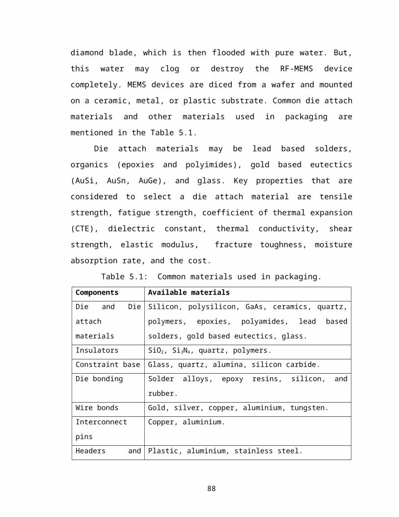
are diced from a wafer and mounted on a ceramic, metal, or plastic substrate. Common
die attach materials and other materials used in packaging are mentioned in the Table 5.1.
86

Die attach materials may be lead based solders, organics (epoxies and
polyimides), gold based eutectics (AuSi, AuSn, AuGe), and glass. Key properties that are
considered to select a die attach material are tensile strength, fatigue strength, coefficient
of thermal expansion (CTE), dielectric constant, thermal conductivity, shear strength,
elastic modulus, fracture toughness, moisture absorption rate, and the cost.
Table 5.1: Common materials used in packaging.
Components Available materials
Die and Die attach
materials
Silicon, polysilicon, GaAs, ceramics, quartz, polymers, epoxies,
polyamides, lead based solders, gold based eutectics, glass.
Insulators SiO2, Si3N4, quartz, polymers.
Constraint base Glass, quartz, alumina, silicon carbide.
Die bonding Solder alloys, epoxy resins, silicon, and rubber.
Wire bonds Gold, silver, copper, aluminium, tungsten.
Interconnect pins Copper, aluminium.
Headers and casings Plastic, aluminium, stainless steel.
The die attach material should strongly stick to the substrate so that the die cannot
move relative to the substrate so that MEMS alignment is not disturbed. Fracture
toughness of materials is needed as it provides the material resistance to failure. The CTE
mismatch between the die attach, silicon and substrate may result in undesirable stresses
causing cracks in the bond. The CTE of the substrate must match the CTE of the die
attach materials in order to minimize the thermal-mechanical stresses in package.
Thermal conductivity becomes important when the attached material have to
conduct heat from die to the substrate. Thermal mismatch between the die and the board
can lead to fatigue fracture. High dielectric constant causes cross talk between modes
because it is directly proportional to the capacitance. High loss tangent signifies high
dielectric absorption that causes the signals to degrade their amplitude and frequency.
Bonds of these materials are highly resistant to fatigue, but die cracking can occur
due to the transfer of high mismatch stress to the device. This stress can be reduced using
organic die attach materials. But, these cannot be used for ceramic packages because the
higher temperature needed to produce seal after the die attach process. Seal may change
87
the properties of the adhesive. Common organic die attach materials are epoxies,
silicones, and polyimides.
5.3: Basic elements of a package
Packaging of MEMS is very much complex as they provide protection from the
environment, sometimes these facilitate interaction with the environment to compute or
influence the preferred physical or chemical properties. There are four basic elements
defined in a functional package as illustrated in the Figure 5.2.
Figure 5.2: Elements of the package.
(a) Device: It may be a surface micromachined cantilever beam, or a diaphragm. It
can also be a microchannel die. The die is the device that is diced from a silicon
wafer.
(b) Wiring or routing: The next key element of the system is its wiring structure that
facilitates the path between the device and the bottom of the package that will
finally connect to the printed wiring board (PWB).
(c) Packaging enclosure: The enclosure of a package is another important element
that protects the device, its wiring structure, and chip level interconnects. The
other functions of enclosure are heat management and handling.
(d) Board level joining system: Flip chip, metal leads, ball grid array, etc, are some
methods employed for the board level joining system.
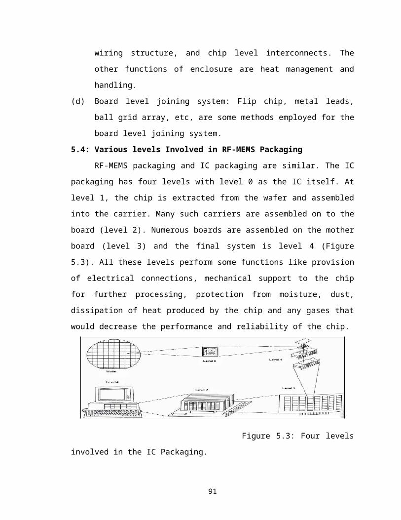
5.4: Various levels Involved in RF-MEMS Packaging
RF-MEMS packaging and IC packaging are similar. The IC packaging has four
levels with level 0 as the IC itself. At level 1, the chip is extracted from the wafer and
assembled into the carrier. Many such carriers are assembled on to the board (level 2).
Numerous boards are assembled on the mother board (level 3) and the final system is
level 4 (Figure 5.3). All these levels perform some functions like provision of electrical
88

connections, mechanical support to the chip for further processing, protection from
moisture, dust, dissipation of heat produced by the chip and any gases that would
decrease the performance and reliability of the chip.
Figure 5.3: Four levels involved in the IC Packaging.
RF-MEMS packaging involves three levels that are represented in the Figure 5.4:
(a) Die level packaging (0-level packaging).
(b) Device level packaging (1-level packaging).
(c) System level packaging (2-level packaging).
5.4.1: Die-level packaging (zero-level packaging)
This level of packaging creates an on-wafer device sealed cavity for the fragile
MEMS device, taken to the wafer during wafer processing, before die singulation. At this
level, assembly and protection of many fragile components (diaphragm, cantilever,
micro-valves, micro-pumps, etc) is done on the silicon wafer. The key objectives of this
level packaging are:
(a) Protecting the die or other heart elements from plastic buckling and
cracking.
(b) Providing essential electrical and mechanical isolation of all these
elements.
(c) Making sure that the system functions at both the standard and overloaded
conditions.
5.4.2: Device level packaging (first-level packaging)
This level of packaging consists of basically the package, also called the chip
capsule (metal can, plastic package, ceramic package) and/or the leads for
interconnecting the chip to the physical world. This level of packaging needs the insertion
89

of proper signal conditioning and processing that in most cases includes electric bridges
and signal conditioning circuitry for sensors and actuators.
Figure 5.4: Three levels of packaging.
5.4.3: System-level packaging (second-level-packaging)
Mounting a first-level packaged device to a board is termed system level
packaging. Second level packaging comprises of the packaging of primary signal
circuitry with the die, or central main element unit. System packaging needs appropriate
mechanical and thermal isolation as well as electromagnetic shielding of the circuitry.
5.5: Fundamental packaging operations
The fundamental operations involved in the packaging of RF-MEMS are:
5.5.1: Die preparation
In this process, the wafer is singulated into individual dice during preparation for
assembly. Die preparation involves two main steps, namely, wafer mounting and wafer
sawing. Wafer mounting process provides support for the wafer to make easy the wafer
processing employing wafer saw through die attach. During wafer mounting process, the
wafer and a wafer frame are, at the same time, attached on a wafer or dicing tape. The
wafer frame may be made of plastic or metal, but it should be resistant to warping,
bending, corrosion, and heat.
The dicing tape (also called wafer film) is just a PVC sheet with synthetic
adhesive on one side to hold both the wafer and the wafer frame. The wafer film or tape
should be flexible yet tough and strong, and also have low impurity levels. Wafer sawing
process is carried after wafer mounting. In this step, the wafer saw actually cuts the wafer
into individual dice for assemblage in RF-MEMS packages.
90
5.5.2: Die attach
Die attach process involves attaching the silicon chip to the die cavity or pad of
the support structure (e.g., the lead frame) of the package. There are two familiar die
attach processes: adhesive die attach and eutectic die attach. First process employs
adhesives (epoxy, polyimide, silver-filled glass) to mount the die on the die pad or die
cavity. The adhesive is first put in limited amounts on the die pad or die cavity. For
mounting the die, it is then driven out from the wafer by one or more ejector needles.
Eutectic die attach process is usually engaged in hermetic packages. This process
employs a eutectic alloy to attach the die to the cavity. A eutectic alloy has low melting
point feasible for the metals combined in the alloy. In semiconductor packaging, the most
frequently used die attach alloy is Au-Sn eutectic alloy.
5.5.3: Wire bonding
The wire bonding tightly attaches back side of a chip to the suitable substrate
location, or package bottom as illustrated in the Figure 5.5. The wires are then bonded or
welded, one at a time, using a particular instrument, wedge or capillary and a
combination of heat, pressure and ultrasonic energy. The various types of wire bonding
are:
a) Thermo-compression bonding: This type of bonding results when two metal
surfaces are brought in close contact during a controlled time, temperature, and
pressure cycle. During this cycle, the wire and the metal beneath, experience
plastic deformation and atomic diffusion between the bonding pad and the wire.
Figure 5.5: Circuit with its wire bonds.
91

b) Ultrasonic bonding: In this low temperature process the source of energy
employed for the metal welding is a transducer. This transducer vibrates the
bonding tool in a frequency range 20-60 kHz.
c) Thermo-sonic bonding: In this type of bonding, ultrasonic energy is combined
with the ball bonding capillary technique of thermo-compression bonding.
5.5.4: Testing
The testing is done for any necessary rework to be accomplished sensibly and at
the same quality level as the initial manufacturing process. Testing can be performed at
the three levels:
1) Wafer level testing:
Wafer level testing deals with mostly material analysis. This is performed with
the help of scanning electron microscopy (SEM), X-Ray microprobe spectroscopy,
transmission electron spectroscopy (TEM), Auger electron spectroscopy, or
Optoelectronic Holography (OEH). The internal microstructure of materials exhibit much
influence on properties of materials. As the dimensions reduce, requirements for low
level contaminant detection, and control becomes vital.
2) Package level testing:
Hermetic or plastic enclosures have electronic components to protect from
physical damage and the undesirable effects of gaseous ambient products. As a result,
package level tests have been developed to make sure the performance and reliability of
the package. These tests are helpful in computing the quality of package. These tests
facilitate an estimate of reliability of the package.
3) Component and board level physical testing:
These include automatic optical testing, solder joint inspection, plating thickness,
and environmental testing. For qualification of a part or printed circuit board (PCB),
physical tests are often considered to be final hurdles that can bring into focus some non-
functionalities. However, complete physical and mechanical confirmation is impossible,
yet the growing inspection has greatly enhanced reliability and quality.
5.5.5: Hermetic Sealing
This process of hermetic sealing confines the MEMS packages within an inert
environment. The process involves in hermetic sealing are:
92

Fused metal sealing,
Welding,
Soldering,
Brazing, and
Glass sealing.
5.5.6: Marking
In the marking process, identification, traceability, and distinguishing marks are
put on the package. The familiar information marked on the package is the device name,
company logo, date code, and lot ID etc. Some marks are put on the package during
assembly and some marks are put on the package during test. There are two frequently
used marking processes: (a) Ink marking (b) Laser marking.
For the most cases, frequently used ink marking process for semiconductor
products is pad printing. It involves transfer of an ink pattern from the plate (that is a flat
block with pattern depressions that are filled with ink) to the package, using a silicone
rubber stamp pad. Silicone rubber repels ink, making the transfer of the ink pattern clean
and well-organized.
Figure 5.6: Single chip packaging.
5.6: State-of-the-art packaging of MEMS
State-of-the-art packaging of MEMS can be divided into three main categories:
Single chip packaging,
Wafer level packaging,
Multi-chip modules.
5.6.1: Single chip packaging
This packaging method is for characteristic IC standard packages like ceramic
packages or pre-formed injected molded packages. The single chips are given with
protective layers to shield the susceptible structures and circuits from environmental
influences. MEMS are diced then released to protect them from the sawing process. Die
93

are then packaged in ceramic cavity, metal can, glass and pre-molded plastic as illustrated
in the Figure.5.6.
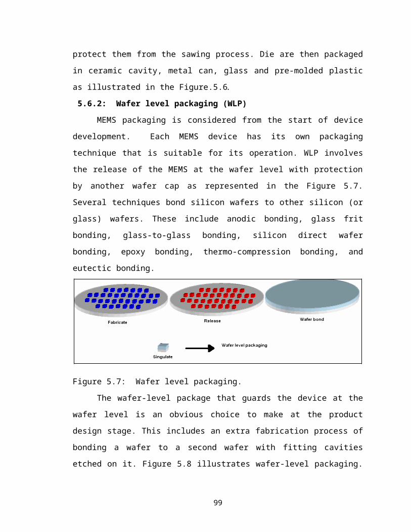
5.6.2: Wafer level packaging (WLP)
MEMS packaging is considered from the start of device development. Each
MEMS device has its own packaging technique that is suitable for its operation. WLP
involves the release of the MEMS at the wafer level with protection by another wafer cap
as represented in the Figure 5.7. Several techniques bond silicon wafers to other silicon
(or glass) wafers. These include anodic bonding, glass frit bonding, glass-to-glass
bonding, silicon direct wafer bonding, epoxy bonding, thermo-compression bonding, and
eutectic bonding.
Figure 5.7: Wafer level packaging.
The wafer-level package that guards the device at the wafer level is an obvious
choice to make at the product design stage. This includes an extra fabrication process of
bonding a wafer to a second wafer with fitting cavities etched on it. Figure 5.8 illustrates
wafer-level packaging. This facilitates the MEMS device to move freely in inert
atmosphere with hermetic bonding that avoids any contamination of the structure.
Figure 5.8: Silicon wafer-level packaging of RF-MEMS.
5.6.3: Multi chip modules
94

The multichip module-deposited (MCM-D) process is the more traditional
approach. It engages the packaging of different devices (electronics, sensors, actuators
etc) in a single module to make elegant miniaturized systems. The expenditure of
packaging in this method is significantly reduced. In this process, the interconnect layers
are first deposited on the substrate, and then the die is mounted on the interconnect
layers. The interconnection is mainly done by wire bonding.
Multichip module (MCM) packaging gives a well-organized answer to integrate
ICs and MEMS for the reason that it provides a base for various die types in a same
substrate without altering fabrication processes. Various types of MCMs are the MCM-C
(ceramic-based multichip module), and MCM-V (vertical multichip module). Figure 5.9
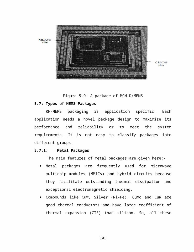
shows an image of package of MCM-D/MEMS.
Figure 5.9: A package of MCM-D/MEMS
5.7: Types of MEMS Packages
RF-MEMS packaging is application specific. Each application needs a novel
package design to maximize its performance and reliability or to meet the system
requirements. It is not easy to classify packages into different groups.
5.7.1: Metal Packages
The main features of metal packages are given here:-
Metal packages are frequently used for microwave multichip modules (MMICs)
and hybrid circuits because they facilitate outstanding thermal dissipation and
exceptional electromagnetic shielding.
95

Compounds like CuW, Silver (Ni-Fe), CuMo and CuW are good thermal
conductors and have large coefficient of thermal expansion (CTE) than silicon.
So, all these metals, with gold, silver or copper plating are good choices for
MEMS packages.
They can have a bulky internal volume with good mechanical reliability.
The package can use either an integrated base plus sidewalls with a lid or it can
have a separate base, sidewalls, and lid. Inside the package, ceramic substrates or
chip carriers are required for use with the feedthroughs. The selection of the
appropriate metal can be vital and decisive.
Prior to finishing assembly, baking is frequently performed to drive out any
trapped gas or moisture. As a result, the occurrences of failures related to
corrosion are significantly decreased.
The feedthroughs that are required in metal packages affect hermeticity. These
feedthroughs are generally made of glass or ceramic. Each method either glass
seal or conductor feedthroughs has its weak points. During handling and thermal
cycling, glass may crack. The conductor is not be sealed well due to metallurgical
reasons.
During assembly, the maximum temperature remedial epoxies or solders should
be employed first and then temperatures are reduced gradually in steps until the
final lid seal is done at the minimum temperature to prevent damaging of the
earlier steps by the later steps. Au-Sn is a normally used solder that performs fine
when the two materials to be bonded have matching CTEs. The Au-Sn inter-
metallic tends to be brittle and can contain stresses of only low magnitudes.
5.7.2: Ceramic Packages
Ceramic materials are thin, flexible films. During a characteristic process, the
films are stretched across a frame. On each layer, metal lines are deposited using thick-
film processing like screen printing. Via holes for interlayer interconnects are drilled or
punched. After fabrication all of the layers, the unfired pieces are stacked, aligned and
laminated together. In the end, the part is fired at a high temperature. The MEMS or other
components are then attached into position by solders or organic epoxy.
96
Several features of ceramic packages make them particularly useful for MEMS.
Main features are given below:
(a) They are light in weight and economical, and have small dimensions,
(b) These can be easily mass produced and can be machined to do many different
functions.
(c) They can be made hermetic. The multi-layer ceramic packages permit integration
of multiple RF-MEMS and other components into a single hermetic package.
(d) These are easier in integrating signal distribution lines and feedthroughs. By
incorporating multiple layers of ceramics and interconnect lines, electrical
performance of the package can be tailored to meet design needs.
A number of problems also affect the reliability of this type of package as given
here.
First, the ceramics shrink during the firing step. The amount of shrinkage is
dependent on the number and position of via holes and wells cut into each layer.
For that reason, different layers may shrink more than others creating stress in the
final package.
Second, because ceramic-to-metal adhesion is not as strong as ceramic-to-
ceramic adhesion, sufficient ceramic surface area must be available to make sure
a good bond between layers. This eliminates the possibility of continuous ground
planes for power distribution and shielding. As an alternative, metal grids are
used for these purposes.
Third, the operating temperature and ceramic properties limit the choice of metal
lines. By matching the shrinkage rate of the metal and ceramic, warping can be
eliminated.
Fourth, there is a class of Low Temperature Co-fired Ceramic (LTCC) packages.
The conductors that are generally used are Ag, AgPd, Au, and AuPt. Ag
migration has been reported to occur at high temperatures, high humidity, and
along faults in the ceramic employed in LTCC packages.
Fifth, the metal must not react chemically with the ceramic during the firing
process. The metals most frequently used are W and Mo.
97

5.7.3: Thin-Film Multilayer Packages
Two general technologies are used for thin-film multilayer packages. In one
technology, sheets of polyimide are laminated together similar to that done for the LTCC
packages described above, except a final firing is not required. Each individual sheet is
normally 25 µm and is processed individually using thin-film metal processing. In the
second technique also polyimide is employed, but each layer is spun onto and baked on
the substrate to shape thick layers up to thickness 20 µm. In this method, via holes are
either wet etched or reactive ion etched (RIE).
The polyimide has a relative permittivity around 3.0. Due to low permittivity and thin
layers, the same characteristic impedance lines can be made with less line-to-line
coupling; so, closer spacing of lines is possible. The low permittivity also causes low line
capacitance and so, more rapid circuits are obtained. Figure 5.10 represents a cross-
sectional view of a three-dimensional multilayered package for MEMS structures on
silicon substrate. Passive elements such as filters and matching circuits are formed in
each layer and active devices are assembled on the top layer using flip-chip technology.
Figure 5.10: A cross-sectional view of a three-dimensional multilayered package for
MEMS structures on silicon substrate.
98
5.7.4: Plastic Encapsulated Packages
Plastic encapsulated packages have been broadly used by the IC industry for many
years in almost every application because of their low cost. Plastic packages are not
hermetic and highly reliable. The packages are also prone to cracking in humid
environments during temperature cycling of the assembly of the package. These packages
consist of the IC or the MEMS die attached to the lead frame, electrically interconnected
to input-output leads, and molded in plastic. The plastic encapsulated packages (PEPs)
have benefits over hermetic packages:
The size and weight of plastic packages is significantly reduced as compared to
other packages.
Reliability of plastic encapsulated packages have increases tremendously due to
the improved encapsulant materials, die passivation, and manufacturing
processes.
These packages are less costly than the hermetic packages because of the rigorous
testing and screening required for low volume hermetic parts. Hermetic packages
usually have a higher material cost and are fabricated with more labor intensive
manual processes.
For typical commercial applications, involving frequencies up to 3 GHz, plastic
packages perform better than their other counterparts. Dielectric constant changes
for plastic molding compounds with higher frequencies.
Plastic devices are assembled and packaged on continuous production lines,
unlike the on-demand production of hermetic parts. Thus availability of plastic
packages is much easy.
5.7.5: MOEMS Packaging
Micro-opto-electro-mechanical systems (MOEMS) that are MEMS integrated
with photonics, contribute to the long-established challenges of MEMS with the extra
problems of optical interconnects and of optical surface contamination. By tradition,
switching in the telecommunication industry is performed electrically even in optical
networks. MOEMS facilitates worth mentioning savings in power, cost, and volume.
More importantly, it eliminates problems the electrical switch or router and allows
wavelength division multiplexing (WDM) to reach its peak performance potential.
99

For all optical networks, MOEMS is estimated to have an enormous force on the
market concerning telecommunications. On the whole, the optical component market is
predicted to grow somewhere between 35% and 50% per year in future years. MOEMS
are well located to force the present market in addition to the growing market. The
creation of hermetic optical packaging requirements has resulted in a library of standard
packages and several sources for routine manufacture package. Most MOEMS
applications put extra importance on hermetic packaging because of possible
contamination of the optical surfaces.
Figure 5.11: Flip-chip MEMS package.
5.7.6: Flip-Chip Assembly Technology
Flip chip technology is a very effective assembly method for diverse applications.
Figure 5.11 illustrates the flip-chip design of a MEMS package. However, flip-chip may
not be compatible with the packaging of MEMS that include microstructures uncovered
to the environment. Main features of flip chip Main features of flip chip technique are:
Flip-chip bonding is attractive to the MEMS industry because of its ability to
package closely numerous dice on a single package substrate with multiple levels
of electrical traces. Similar systems can built with wire bonding, but the area
usage will be greater and the number of gold wires within the package may
present a reliability issue.
Flip-chip is the most superior assembly technology for high-frequency
applications as the short bump interconnects decreases parasitic impedances. In
flip chips, an IC die is put on a circuit board with bond pads facing down and
joining the bare die with the substrate.
100
The bumps form electrical contact and a mechanical joint with the die. It reduces
the electrical path, the capacitance and inductance that is mostly suitable for high
RF applications. The reduction in parasitic capacitance and inductance decreases
the signal delay in rapid circuits.
Flip-chip bonding includes the bonding of die, top-face down on a package
substrate.
Electrical connections are made by means of plated solder bumps between bond
pads on the die and metal pads on the substrate.
5.7.7: Wafer Level capping technology
Figure 5.12: Cap wafer process flow.
Wafer level capping technology is a novel and efficient packaging technology
developed for MEMS devices. It is based upon a 6” wafer-to-wafer bonding process. The
basic manufacturing process flow for the cap wafer is illustrated in Figure 5.12. The flow
consists of only three Litho steps of which one Litho step is only intended to enable
dicing of the cap wafer after the wafer to wafer bonding process. This technology is
based upon an AuSn seal and a silicon cap to create hermetic cavities. The low
temperature bonding process is compatible with a definite level of wafer topology and
101
allows bond frame widths of only 80μm, which in combination with optimized bond
frame crossings allow RF-MEMS devices with good RF-performance. This bonding
process is able to generate reliable hermetic joints on 6” wafer level.
The actual bonding begins at the melting temperature of the Sn (232°C).
As the bonding force the excess of Sn gets squeezed to edges of the seal while the
remaining Sn at the Au interfaces is fully altered into AuSn intermetallics. Figure 5.13
shows an image of a cross-section made across the seal of a bonded sample. From this
technique, the results showed significant higher fracture strengths for the backside of
those wafers that had been open to the extra etching process.
Figure 5.13: Cross-section of AuSn seal.
5.8: Summary
MEMS is the integration of mechanical elements, sensors, actuators, and
electronics on a common silicon substrate through the utilization of microfabrication
technology. Similar to Integrated Circuits (IC), packaging of MEMS needs environmental
protection, electrical signal pathway, mechanical support, and thermal management
paths. MEMS packaging presents unique challenges compared to IC packaging due to the
diversity of MEMS devices and the requirement that many of these devices are in
continuous and intimate contact with their environment. Thus, special techniques and
materials are necessary (non-standard) in making MEMS packaging.
The current methods involve bonding techniques ceramics, metal or plastic
packaging, reactive sealing (PECVD or LPCVD), hybrid packaging such as multichip
modules (MCMs) and flip-chip technologies (e.g. MEMS and microelectronics on a
common substrate). Essentially two methods for device packaging can be defined: The
102
first-level packaging (the chip capsule and the leads for interconnecting the chip to the
outside world) and the zero-level package (or wafer level package where the package is
designed and fabricated at the same time the device is fabricated). For zero-level
packaging two approaches can be distinguished: wafer bonding and surface
micromachining techniques.
Recent growth in the wireless communication expands the application area for the
RF-MEMS systems in a package (e.g. GSM, Bluetooth) and the interest in RF-MEMS
sensing devices (e.g. GPS, radar). The main requirements for the RF-MEMS package
technology are:
i) Low parasitic chip/substrate interconnection
ii) Passive integration substrates (matched impedance, high quality
passive R-L-C components),
iii) Package to next level interconnect (low insertion loss, electro-magnetic
shielding),
iv) First time right design methodology (automatic design).
103