· web view15. to reduce the input voltage transformer is used. 16. to increase the input...
TRANSCRIPT

REVISION QUESTIONS
ELECTRONIC CIRCUITS SW 233
1

CH 1Answer the following questions:1. List some of electric and electronic components:
-………………………………………………….
-………………………………………………….
- ……………………….………….……………..
-…………………………………………………..
-………………………………………………….
2. Variable resistor is used as:-…………………………………………………..
-………………………………………………….
3. There are many types of resistors.-…………………………………………………..
-………………………………………………….
-………………………………………………….
4. There are many types of capacitors.-…………………………………………………..
-………………………………………………….
-………………………………………………….
5. There are many types of coils.-…………………………………………………..
-………………………………………………….
-………………………………………………….
6. Factors affect the wired resistor value are:-…………………………………….
-…………………………….………
-…………………………………….
2

7. Capacitors prevent …………………… and allow …………...……. to pass.
8. R1, R2, R3 are connected in parallel, the equivalent resistance is ……………………………………….……….
9. R1 = 250 KΏ, R2 = 5000Ώ, R3 = .5 MΏ are connected in series, the equivalent resistance is ………………………..………………..
10. Four equal resistors (3.6 KΏ) are connected in parallel. The equivalent resistance is ………………………….
11. Calculate the time constant for RC circuit if R = 1MΏ, C = 5 nf.………………………………………………………………………………
12. In 3-phase power lines, phase – to – phase voltage is……………….., and phase – to – neutral voltage is ……………………
13. Generator converts ……………………..to………………………..
14. Motor converts ……………………..to………………………
15. To reduce the input voltage …………………………transformer is used.
16. To increase the input voltage ……………………..transformer is used.
17. Transformers are used to prevent ……………………. signal to pass through.
18. The induced E.M.F. across secondary windings is due to …………………………….
19. The resonance frequency FO =…………………..
20. Diode has…………………….resistance in the reverse direction and…………………..resistance in the forward direction.
3

21. Sine waves are considered as …………………………
22. Complex waveforms are considered as …………………………
23. The variation of amplitude (value) with time produces ………………………
24. Frequency is defined as …………………………….…………………….…
25. The periodic time is…………………………………………………………….
26. Voice frequency range from……………Hz to…………Hz.
27. Audio frequency range from……………Hz to…………Hz.
28. Square waveform is composed of ………………………. and number of ……………
harmonics.
29. Saw tooth waveform is composed of …………………… and number of ……………
harmonics.
30. If the pulse time tends to zero, the pulse is called ………………………….
31. If the periodic time of square wave is 100 ms, and the mark time is 60 ms. The space time is ……………………
32. Calculate the periodic time (T) if the frequency 20 KHz. (T = ………….)
33. Calculate the periodic time of a square wave if M/S = 1 ………………………..…………………………………..
34. An audio frequency with 10 KHz,* Fundamental = …………………………
* Even harmonics:
- …………………………
- …………………………
4

36. A voice frequency with 3 kHz,* Fundamental = …………………………
* Odd harmonics: - …………………………
-…………………………
37. A complex waveform with 10 KHz,* Fundamental = …………………………
* Harmonics: …………………………
-…………………………
-…………………………
-…………………………
-…………………………
38. The higher harmonic the …………………..frequency
39. The higher harmonic the …………………..periodic time
40. The higher harmonic the …………………..amplitude.
41. The fundamental frequency equals the ………………..frequency.
42. From the figure shown, calculate:a) M =……………………….… V
b) S =…………………………. 20 secc) M/S =…………………….…
d) T =………………………… M S M S Me) f =..........................................
t
5

CH 2Fill in the spaces:
1) Amplifiers and oscillators are ……………………… networks.
2) Resistors, attenuators and transformers are …………………. networks.
3) The average value of H.W.R. is approximately………………….. Vp.
4) The average value of F.W.R. is approximately ……….………… Vp.
5) The Vrms value of sine wave is ………………………..Vp.
6) The average value of sine wave is ………………………..Vp.
7. To reduce the AC variation of the rectifier waveform, a ………………………. is used.
8) The amplitude of the ripple is determined by the …………..………….. and …………………… values.
9) ……………………………… is the terminal voltage of the power supply when the load current is zero.
10) An important factor that must be considered in choosing diodes in power supplies is …………………………………
11) In L-C smoothing circuit inductor must has a …………………… inductance.
12) A …………………. is used to maintain the terminal voltage constant.
6

Mark ( √ ) on the correct answer:
1) Active circuits do not need power source. ( )
2) Passive circuits need power source. ( )
3) Active circuits need D.C. to work. ( )
4) Power supplies are the circuits that convert DC power to AC power.( )
5) Diode will conduct if the potential across it is zero. ( )
6) Reservoir (filtering) capacitor must have small capacitance. ( )
7) Reservoir (filtering) capacitor is in charging state when the main voltage increasing.( )
8) If the main supply is 120 V., no load voltage will be equal to 218 Vac ( )
9) PIV is the maximum voltage the device has to sustain during the conducting half cycle. ( )
10) Smoothing circuit is considered as high pass filter. ( )
11) Smoothing circuit is used to attenuate the ripple. ( )
12) In R-C smoothing circuit, () must be very small compared with the periodic time of
the ripple. ( )
13) It is easier to smooth out F.W.R. ripple than H.W.R. ripple due to its low frequency. ( )
14) The periodic time of F.W.R. is greater than the periodic time of H.W.R.
7
( )15) The frequency of F.W.R. is greater than the frequency of H.W.R. ( )
16) Zener diode operates at its breakdown voltage. ( )
17) Zener shunt regulator is better and more efficient than series regulator. ( )
18) Transistors may be used as overload protection. ( )
19) DC/DC power supply converts a smaller DC input voltage to a larger DC output voltage. ( )
8

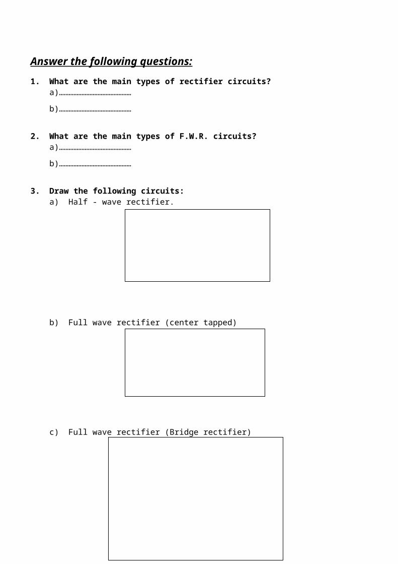
Answer the following questions:1. What are the main types of rectifier circuits?
a)………………………………………
b)………………………………………
2. What are the main types of F.W.R. circuits?a)………………………………………
b)………………………………………
3. Draw the following circuits:a) Half - wave rectifier.
b) Full wave rectifier (center tapped)
c) Full wave rectifier (Bridge rectifier)
9

4. Draw R-C smoothing circuit.
5. Draw L-C smoothing circuit.
6. What are the smoothing circuit types?a)…………………………………………..
b)………………………………………….
7. What are the regulated power supply types?
a)…………………………………………………..
b)…………………………………………………..
8. Draw shunt regulation circuit.
10

9. Draw series regulation circuit.
10. A Zener diode stabilizer 2 watt is used to provide 48 volt stabilized supply to a variable load resistor and if the input voltage is 60 volt,
*Calculate:a) The series resistance R required ………………………………………………………………………………................
………………………………………………………………………………................
b) The diode current Iz when the load resistance decreases to 2000 Ω.………………………………………………………………………………………….
………………………………………………………………………………………….
………………………………………………………………………………………….
………………………………………………………………………………………….
11. A Zener diode stabilizer circuit hasVz = 20 voltIz(min) = 20 mAVin = 50 volt + 10 %IL = 30 mA
*Calculate:a) The series resistance R required.………………………………………………………………………………………….
………………………………………………………………………………………….
………………………………………………………………………………………….
11

b) The power dissipated in the diode Pz when the supply voltage is 55 volt. ………………………………………………………………………………………….
………………………………………………………………………………………….
………………………………………………………………………………………….
………………………………………………………………………………………….
………………………………………………………………………………………….
………………………………………………………………………………………….
12
12. A Zener diode stabilizer 2.4 watt is used to provide 48 volt stabilized supply to a variable load resistor and if the input voltage is 50 v,
*Calculate:a) The series resistance R required ………………………………………………………………………………................
………………………………………………………………………………................
b) The diode current Iz when the load resistance decreases to 2000 Ω.………………………………………………………………………………………….
………………………………………………………………………………………….
………………………………………………………………………………………….
c) The power dissipated Pz …………………………………………………………
13. A Zener diode stabilizer circuit hasVz = 40 voltIz(min) = 20 mAVin = 100 volt + 10 %IL = 30 mA
*Calculate:b) The series resistance R required.………………………………………………………………………………………….
………………………………………………………………………………………….
………………………………………………………………………………………….
b) The power dissipated in the diode Pz when the supply voltage is 55 volt. ………………………………………………………………………………………….
………………………………………………………………………………………….
………………………………………………………………………………………….
………………………………………………………………………………………….
………………………………………………………………………………………….
………………………………………………………………………………………….
13

14 Give an expression of each following statement.
a) A circuit is usually used to convert the mains into DC voltage of various magnitudes.
………………………………………………………………………………………….
b) To reduce the AC variation of the rectified waveform.
………………………………………………………………………………………….
c) The terminal voltage of the power unit when the load current is zero.
………………………………………………………………………………………….
d) An important factor that must be considered in choosing the diodes for DC power supplies.
………………………………………………………………………………………….
e) The AC ripple may be reduced using a low pass filter.
………………………………………………………………………………………….
f) A circuit that generates a small DC output voltage from a large DC input voltage.
………………………………………………………………………………………….
g) A circuit provides a constant regulated output voltage without any interruption.
………………………………………………………………………………………….
14

CH 3
Answer the following questions:
The A-Stable MV circuit used to produce an alarm application.If R1= 1KΩ, C =1 µF and F=1KHz.
*Calculate: a) Resistor R2
…………………………………………………………………………………………………………
……………………………………………………………………………………
b) The flashing frequency…………………………………………………………………………………………………………
……………………………………………………………………………………
c) High time (Mark time) …………………………………………………………………………………………………………
……………………………………………………………………………………
d) Low time (Space time)…………………………………………………………………………………………………………
……………………………………………………………………………………
e) Duty cycle…………………………………………………………………………………………………………
……………………………………………………………………………………
f) M/S ratio…………………………………………………………………………………………………………
……………………………………………………………………………………
15

The A-Stable MV circuit used to produce an alarm application.
If R1= 1KΩ, R2= 49.5KΩ and C =0.1 µF.
*Calculate:
a) The flashing frequency…………………………………………………………………………………………………………
……………………………………………………………………………………
b) High time (Mark time)…………………………………………………………………………………………………………
……………………………………………………………………………………
c) Low time (Space time)…………………………………………………………………………………………………………
……………………………………………………………………………………
d) Duty cycle…………………………………………………………………………………………………………
……………………………………………………………………………………
e) M/S ratio…………………………………………………………………………………………………………
……………………………………………………………………………………
16

Draw the following circuits:
A) Voltage doubler B) Analog switch
C) RC differentiator (square wave input) D) RC integrator (square wave input)
E) Sample – and - hold F) OP-AMP Schematic symbol
17
G) Draw the output waveforms for differentiator and integrator.
Vin
t
Input signal
Vo
t
Differentiator output
Vo
t
Integrator output
18
Complete the following statements:
1) A-stable MV may be known as …………………………….….…
2) Efficiency is better in a ………….voltage regulator than in a …………voltage regulator.
3) Bi-stable MV may be known as …………………………….……
4) Mono-stable MV may be known as ………………………………
5) To produce good differentiation, the time constant (RC) must be …………… compared to the periodic time of the ……………… signal.
6) To produce good integration, the time constant (RC) must be …………… compared to the periodic time of the ……………… signal.
7) .………………………… allows low frequencies to pass through and attenuates all …………… frequencies.
8) ……………………………… allows only …………… frequencies to pass through and attenuates all low frequencies.
9) Band pass filter allows only a ……………of frequencies to pass through and all other frequencies …………. and be……..…….. that band.
10) .……………………………. cuts off a band of frequencies and allow all other frequencies …………….. and ……………….. that band to pass through.
11) …………………are circuits that compare …………. (values) and …………. (binary), check for correction (Parity check bits).
12) A ……………………………….IC compares two input frequencies and produces a logical 0 or 1 output when the frequency being compared are…………. or are………… or less than the ………………… level.
13) ……………………….. are a means of doubling the peak-rectified voltage from a transformer or AC power line.
14)…………………………. can be connected with external resistors and capacitors to form a-stable, bi-stable, or mono-stable multi-vibrators.
19

Put ( √ ) in front of the correct answer:
1) A-stable MV has no stable state ( )
2) Bi-stable has only one stable state ( )
3) Mono-stable has two stable states. ( )
4) The output of RC differentiator is taken across R. ( )
5) The output of RC integrator is taken across C. ( )
6) The op amp has very low input impedance. ( )
7) The input impedance of the IC Op-Amp is very low. ( )
8) A shunt voltage regulator is one which has the regulating element in
9) Parallel with the output. ( )
10) The operation amplifier has a high open loop gain. ( )
11) A regulated supply voltage is important for digital circuits to provide specific values for the high and low voltages. ( )
12) The OP-AMP schematic symbol is often used as voltage comparators. ( )
13) The differentiator is a high pass filter, which when fed with a square wave reproduces the high-frequency components only. ( )
14) The integrator is a low pass filter which when fed with a square wave reproduces the low-frequency components only. ( )
20
Give the technical term (an expression) of each statement:
1) A circuit that holds an output voltage at a predetermined level regardless of
input voltage changes or output load changes
……………………………………………….
2) A highly regulated voltage source for circuits where the accuracy of the voltage source is very important.
……………………………………………….
3) The amount of dc output voltage can be made twice the ac input by using.……………………………………………….
4) Compares two analog input voltages and produces a logical 0 or 1 output when the voltages being compared are equal or are greater or less than the reference level.
………………………………………………..
5) An IC that replaces a mechanical switch. A logic input controls when the bilateral switch is on or off.
………………………………………………
6) IC is used to “sample” an analog input signal. This sample-input voltage is frozen in time by being stored in an external capacitor.
………………………………………………..
7) Converts a digital (binary) input into a voltage whose magnitude is proportional to the value of the digital signal.
……………………………………………….
21
A sample-and-hold / Voltage doublers / Multi-vibrator / Phase splitter / Differentiator/ (D/A) converter / Bi-stable MV / Phase inverter / Low pass filter / Difference op amp / (A/D) converter / Voltage comparator / Mono stable MV / Band stop filter / Voltage reference / Analog switch / A-stable MV / High pass filter / summing op amp Integrator / Oscilloscope / Power supply / Rectifier / Op amp multiplier / Voltage regulator
8) Converts a continuously varying analog input voltage into a proportional digital output.
……………………………………………..
9) A circuit whose output is square wave or rectangular wave.………………………………………………
10) An oscillator circuit that generates a continuous flow of digital pulses.………………………………………………
11) MV, an input pulse reverses the state of the output………………….……………………………………………..
12)MV, produces a single output pulse of a given time duration…………………………………………………………..
13)MV is always in one of two stable states.……………………………………………..
14)Produces two equal (amplified) signals.…………………………………………….
15)Produces two signals of equal amplitude, but 180o out of phase.……………………………………………..
16)High pass filters which produces fast rising and falling edges in the form of positive and negative spikes.
…………………………………………….
17)Produces an output voltage proportional to the total.…………………………………………….
18)Provides an output, which is proportional to the difference in the output signal.…………………………………………….
19)Allow low frequency to pass through and attenuates all high frequencies.……………………………………………..
20) A circuit produces spikes at the output.……………………………………………..
22

23

Choose the correct answer:
1. The two output signals of a phase inverter:a) Are in phase with each other.b) Are in phase with the input signal.c) Are 180° out-of-phase with each other.d) Are 90° out-of-phase with the input signal.
2. The phase comparator ………….a) Generates a frequency.b) Is not a necessary component of the PLL circuit.c) Compares the phase of two input signals.d) Divides the frequency applied to its input.
3. In a good integrating circuit, the time constant must be:a) Long compared to the period of the input waveform.b) Equal to the period of the input waveform.c) Short compared to the period of the input waveform.d) One half the period of the input waveform.
4. The process of producing an output signal that represents the instantaneous changes of the input signal is called:a) Differentiation.b) Integration.c) Amplification.d) Comparison.
5. Another name for the a-stable multi-vibrator isa) Flip-flop.b) One-shot.c) Free-running.d) Single-shot.
6. Two inputs scaling summer has (RF/R1) ratio of 8/1 and 4/1. If each input is one volt, the output voltage isa) +12 volts.b) –12 volts.c) –15 volts.d) +15 volts.
7. An active filter that has minimum gain below and above two frequencies but has high gain between these two frequencies is calleda) A high pass filter.b) A band pass filter.c) A band reject filter.d) A low pass filter.
8. Which of the following statements is true:
24
a) The output of an RL integrator is across R.b) The output of an RC integrator is across R.c) The input of an RL integrator is applied to L only.d) All of the above.
9. In a good differentiating circuit, the time constant must be:a) Long compared to the period of the input waveform.b) Equal the period of the input waveform.c) Short compared to the period of the input waveform.d) Twice the period of the input waveform.
10. An active filter that has high gain below the cutoff frequency but has low gain above the cutoff frequency is calleda) A high pass filter.b) A band pass filter.c) A band reject filter.d) A low pass filter.
11. The process of producing an output signal that represents the sum of the incremental changes in the input signal over a period of time is called:a) Differentiation.b) Integration.c) Amplification.d) Comparison.
Answer the following questions: 25

1) What are the main types of filters?a) …………………………………..
b) …………………………………..
c) …………………………………..
d) …………………………………..
2) What are the main circuits of filters?a) …………………………………..
b) …………………………………..
c) …………………………………..
d) …………………………………..
3) The OP-AMP has the following propertiesa) …………………………………..
b) …………………………………..
c) …………………………………..
d) …………………………………..
4) Write the name of each curve. Gain Gain
F F Fc1 Fc2 Fc1
1)................................... 2)........................................
26