vhdl model reference manual - redrapids.com model reference manual 797 north grove rd, suite 101...
TRANSCRIPT
Publication No. REF-003-000-R02
Red Rapids
VHDL Model
Reference Manual
797 North Grove Rd, Suite 101
Richardson, TX 75081
Phone: (972) 671-9570
www.redrapids.com

Publication No. REF-003-000-R02
Red Rapids
Red Rapids reserves the right to alter product specifications or discontinue any product without notice. All products are sold subject to the terms and conditions of sale supplied at the time of order acknowledgment. This product is not designed, authorized, or warranted for use in a life-
support system or other critical application.
All trademark and registered trademarks are the property of their respective owners.
Copyright © 2014, Red Rapids, Inc. All rights reserved.

Publication No. REF-003-000-R02
Red Rapids Page iii
Table of Contents 1.0 Introduction ....................................................................................................................... 1 1.1 Conventions .................................................................................................................. 1 1.2 Revision History ............................................................................................................ 2 2.0 ADC Interface (adc_interface.vhd) .................................................................................... 3 2.1 Dynamic Phase Alignment ............................................................................................ 3 2.2 Data Formatter .............................................................................................................. 3 3.0 BAR0 Decoder (bar0_decoder.vhd) .................................................................................. 4 3.1 Host Bus Interface ......................................................................................................... 4 3.2 Software Reset .............................................................................................................. 4 3.3 Clock Initialization ......................................................................................................... 4 3.4 Error Capture ................................................................................................................ 5 3.5 Serial Bus Interface ....................................................................................................... 5 3.6 Byte Peripheral Interface ............................................................................................... 5 3.7 Global Status ................................................................................................................. 5 3.8 Interrupt Control ............................................................................................................ 5 3.9 DMA Command/Status .................................................................................................. 5 4.0 BAR2 Channel (bar2_channel.vhd) ................................................................................... 7 4.1 Host Bus Interface ......................................................................................................... 7 4.2 Synchronizer Command/Status ..................................................................................... 7 4.3 Channel Status Capture ................................................................................................ 7 5.0 BAR2 Common (bar2_common.vhd) ................................................................................ 9 5.1 Host Bus Interface ......................................................................................................... 9 5.2 Product Identification ..................................................................................................... 9 5.3 Software Trigger ............................................................................................................ 9 5.4 Demonstration Register ................................................................................................. 9 5.5 Peripheral Device Interface ......................................................................................... 10 6.0 BAR2 Decoder (bar2_decoder.vhd) ................................................................................ 11 6.1 Address Decoder ........................................................................................................ 11 7.0 BPI Flash (bpi_flash.vhd & bpi_flash_stub.vhd) .............................................................. 12 7.1 Theory of Operation .................................................................................................... 12 8.0 Clock Crossing (clock_crossing.vhd) .............................................................................. 13 8.1 Input ............................................................................................................................ 13 8.2 Output ......................................................................................................................... 13 9.0 Clock Lock (clock_lock.vhd) ............................................................................................ 14 9.1 Idle State ..................................................................................................................... 14 9.2 Load State ................................................................................................................... 15 9.3 Initialization State ........................................................................................................ 15 9.4 Search State ............................................................................................................... 15 9.5 Monitor State ............................................................................................................... 15 9.6 Adjust State ................................................................................................................. 15 10.0 Clock Route (clock_route.vhd) ........................................................................................ 16 10.1 Clock Sources ............................................................................................................. 16 10.2 Channel Clocks ........................................................................................................... 16 11.0 DAC Interface (dac_interface.vhd) .................................................................................. 17 11.1 Functional Description ................................................................................................. 17 11.2 Data / Clock Alignment ................................................................................................ 17 12.0 DMA on Demand (dma_on_demand.vhd) ....................................................................... 18

Publication No. REF-003-000-R02
Red Rapids Page iv
12.1 Idle State ..................................................................................................................... 18 12.2 Burst Request ............................................................................................................. 19 12.3 Burst Start ................................................................................................................... 19 12.4 Burst End .................................................................................................................... 19 12.5 Burst Complete ........................................................................................................... 19 12.6 Next Page ................................................................................................................... 19 12.7 Burst / Page Counter ................................................................................................... 19 13.0 DMA Read FIFO (dma_read_fifo.vhd) ............................................................................ 20 13.1 DMA FIFO ................................................................................................................... 20 13.2 Channel FIFO .............................................................................................................. 20 13.3 DMA Request .............................................................................................................. 20 14.0 DMA Write FIFO (dma_write_fifo.vhd) ............................................................................ 21 14.1 Channel FIFO .............................................................................................................. 21 14.2 DMA FIFO ................................................................................................................... 21 14.3 DMA Requests ............................................................................................................ 21 15.0 Interrupt Controller (interrupt_controller.vhd) .................................................................. 22 15.1 Monitor ........................................................................................................................ 22 15.2 Interrupt ....................................................................................................................... 22 16.0 Interrupt Timer (interrupt_timer.vhd) ............................................................................... 23 16.1 Response Timer .......................................................................................................... 23 16.2 Timeout Timer ............................................................................................................. 23 17.0 PCI Express (pci_express.vhd) ....................................................................................... 24 17.1 Xilinx 7 Series Integrated Block Plus for PCI Express ................................................. 24 17.2 PLDA EZDMA2 ........................................................................................................... 39 18.0 PCI Performance (pci_performance.vhd) ........................................................................ 43 18.1 DMA Throughput Measurement .................................................................................. 43 18.2 DMA Latency Measurement ........................................................................................ 43 19.0 PCI Transaction Decoder (pci_transaction_decoder.vhd) ............................................... 44 19.1 Target Transactions .................................................................................................... 44 19.2 DMA Transactions ....................................................................................................... 44 20.0 QDR Demo (qdr_demo.vhd) ........................................................................................... 45 20.1 Idle State ..................................................................................................................... 45 20.2 Write State .................................................................................................................. 45 20.3 Read State .................................................................................................................. 46 20.4 Compare State ............................................................................................................ 46 21.0 QDR DLL (qdr_dll.vhd) ................................................................................................... 47 21.1 Idle State ..................................................................................................................... 47 21.2 Initialize State .............................................................................................................. 47 21.3 Reset State ................................................................................................................. 48 21.4 Settle State ................................................................................................................. 48 21.5 Done State .................................................................................................................. 48 22.0 QDR SRAM (qdr_sram.vhd & qdr_sram_stub.vhd) ......................................................... 49 22.1 Static Phase Alignment ............................................................................................... 50 22.2 Dynamic Phase Alignment .......................................................................................... 50 22.3 QDR State Machine .................................................................................................... 50 22.4 Write Transaction State Machine ................................................................................. 51 22.5 Read Transaction State Machine ................................................................................ 51 23.0 RX Datapath (rx_datapath.vhd) ...................................................................................... 53 24.0 RX Flow Control (rx_flow_control.vhd) ............................................................................ 54 24.1 Gate ............................................................................................................................ 54

Publication No. REF-003-000-R02
Red Rapids Page v
24.2 Formatter .................................................................................................................... 54 25.0 Serial Bus (serial_bus.vhd) ............................................................................................. 55 25.1 Clock Divider ............................................................................................................... 55 25.2 Serial Data .................................................................................................................. 55 25.3 Protocol ....................................................................................................................... 55 26.0 Synchronizer (synchronizer.vhd) ..................................................................................... 56 26.1 Idle State ..................................................................................................................... 57 26.2 Initialize State .............................................................................................................. 57 26.3 Prime State ................................................................................................................. 57 26.4 Start Trig State ............................................................................................................ 57 26.5 Stop Trig State ............................................................................................................ 57 26.6 Purge State ................................................................................................................. 57 26.7 Residue State .............................................................................................................. 57 27.0 Transceiver (transceiver.vhd) .......................................................................................... 59 28.0 TX Datapath (tx_datapath.vhd) ....................................................................................... 60 29.0 TX Flow Control (tx_flow_control.vhd) ............................................................................ 61 29.1 Gate ............................................................................................................................ 61 29.2 Formatter .................................................................................................................... 61

Publication No. REF-003-000-R02
Red Rapids Page vi
List of Figures Figure 2-1 ADC Interface Functional Block Diagram ................................................................... 3 Figure 3-1 BAR0 Decoder Functional Block Diagram .................................................................. 4 Figure 4-1 BAR2 Channel Functional Block Diagram .................................................................. 7 Figure 5-1 BAR2 Common Functional Block Diagram ................................................................. 9 Figure 6-1 BAR2 Common Functional Block Diagram ............................................................... 11 Figure 7-1 BPI Flash Functional Block Diagram ........................................................................ 12 Figure 9-1 Clock Lock Functional Block Diagram ...................................................................... 14 Figure 11-1 DAC Interface Functional Block Diagram................................................................ 17 Figure 12-1 DAC DMA on Demand Functional Block Diagram .................................................. 18 Figure 13-1 DMA Read FIFO Functional Block Diagram ........................................................... 20 Figure 14-1 DMA Write FIFO Functional Block Diagram ............................................................ 21 Figure 15-1 Interrupt Controller Functional Block Diagram ........................................................ 22 Figure 16-1 Interrupt Controller Functional Block Diagram ........................................................ 23 Figure 17-1 PCI Express Functional Block Diagram .................................................................. 24 Figure 17-2 PCI Express IP Wizard (Basic Tab) ........................................................................ 26 Figure 17-3 PCI Express IP Wizard (IDs Tab) ........................................................................... 27 Figure 17-4 PCI Express IP Wizard (BARs Tab) ........................................................................ 28 Figure 17-5 PCI Express IP Wizard (Core Capabilities Tab) ...................................................... 29 Figure 17-6 PCI Express IP Wizard (Link Registers Tab) .......................................................... 30 Figure 17-7 PCI Express IP Wizard (Interrupts Tab) .................................................................. 31 Figure 17-8 PCI Express IP Wizard (Power Management Tab) ................................................. 32 Figure 17-9 PCI Express IP Wizard (Extended Capabilities Tab) .............................................. 33 Figure 17-10 PCI Express IP Wizard (Extended Capabilities-2 Tab) ......................................... 34 Figure 17-11 PCI Express IP Wizard (TL Settings Tab) ............................................................. 35 Figure 17-12 PCI Express IP Wizard (DL & DP Settings Tab) ................................................... 36 Figure 17-13 PCI Express IP Wizard (Shared Logic Tab) .......................................................... 37 Figure 17-14 PCI Express IP Wizard (Core Interface Parameters Tab) ..................................... 38 Figure 17-15 EZDMA2 Wizard (General Tab) ............................................................................ 40 Figure 17-16 EZDMA2 Wizard (DMA Tab) ................................................................................ 41 Figure 17-17 EZDMA2 Wizard (Optional Features Tab) ............................................................ 42 Figure 18-1 PCI Performance Functional Block Diagram ........................................................... 43 Figure 19-1 PCI Transaction Decoder Functional Block Diagram .............................................. 44 Figure 20-1 QDR Demo Functional Block Diagram ................................................................... 45 Figure 21-1 QDR DLL Functional Block Diagram ...................................................................... 47 Figure 22-1 QDR SRAM Functional Block Diagram ................................................................... 49 Figure 22-2 QDR State Machine Functional Block Diagram ...................................................... 50 Figure 22-3 Write State Machine Functional Block Diagram ...................................................... 51 Figure 22-4 Read State Machine Functional Block Diagram ...................................................... 52 Figure 23-1 RX Datapath Functional Block Diagram ................................................................. 53 Figure 24-1 RX Flow Control Functional Block Diagram ............................................................ 54 Figure 25-1 Serial Functional Block Diagram ............................................................................. 55 Figure 26-1 Synchronizer Functional Block Diagram ................................................................. 56 Figure 27-1 Transceiver Functional Block Diagram ................................................................... 59 Figure 28-1 TX Datapath Functional Block Diagram .................................................................. 60 Figure 29-1 TX Flow Control Functional Block Diagram ............................................................ 61
Publication No. REF-003-000-R02
Red Rapids Page 1
1.0 Introduction
Red Rapids provides VDHL design source to demonstrate the key features of FPGA based products. The source code is organized into VHDL models that address a specific function of the design. Most models are parameterized so that they can be used across multiple products by defining constants that encapsulate the unique features of each product.
The following is a list of typical functions performed by a model:
Interfaces to external devices connected to the FPGA.
Address decoders that connect command/status registers to a bus.
DMA functions to manage the movement of data over a bus.
Controllers to initialize hardware.
The most recent release of this document is available for download from the Red Rapids website (www.redrapids.com).
1.1 Conventions
This manual uses the following conventions:
Hexadecimal numbers are prefixed by “0x” (e.g. 0x00058C).
Italic font is used for names of registers.
Blue line is used in figures to denote VHDL code within a model.
Green line is used in figures to identify models instantiated within a model.
Text in this format highlights useful or important information.
! Text shown in this format is a warning. It describes a situation that could potentially damage your equipment. Please read each warning carefully.
The following are some of the acronyms and abbreviations used in this manual.
ADC Analog to Digital Converter
AXI Advanced eXtensible Interface
BAR Base Address Register
BPI Byte Peripheral Interface
DAC Digital to Analog Converter
DDR Double Data Rate
DMA Direct Memory Access
DPA Dynamic Phase Alignment
FPGA Field Programmable Gate Array
I2C Inter-Integrated Circuit
PCI Peripheral Component Interconnect
PCIe Peripheral Component Interconnect Express
QDR Quad Data Rate
RX Receiver
SDR Single Data Rate

Publication No. REF-003-000-R02
Red Rapids Page 2
SPI Serial Peripheral Interface
TX Transmitter
1.2 Revision History
Version Date Description
R02 7/14/2015 Added BPI Flash, PCI Performance, QDR Demo, and QDR DLL models. Made extensive changes to QDR SRAM model and removed Clock Init model. Minor updates to the BAR2 Common model and the Xilinx PCIe core description.
R01 4/30/2014 Added Xilinx PCIe and PLDA EZDMA2 core descriptions.
R00 3/19/2014 Initial release.

Publication No. REF-003-000-R02
Red Rapids Page 3
2.0 ADC Interface (adc_interface.vhd)
The ADC Interface, shown in Figure 2-1, is used to capture data supplied from an external analog-to-digital converter (ADC).
Figure 2-1 ADC Interface Functional Block Diagram
This model can accommodate any number of ADC channels of arbitrary bus width and will support either single data rate (SDR) or double date rate (DDR) signaling from the device. Very high speed converters frequently use internal demultiplexers to supply sequential samples across multiple ports simultaneously to reduce the data clock speed. This model can be configured for any number of ports and will also support data interleaving on individual DDR pins when that technique is used to minimize the ADC package size.
A typical user application would not change this model.
2.1 Dynamic Phase Alignment
It is impossible to compute a valid setup and hold constraint at the ADC input pins because the min/max timing window usually exceeds the data clock period. This is a common FPGA problem that is solved using dynamic phase alignment techniques. The purpose of the Clock Lock function is to perform phase alignment using the data clock forwarded from the ADC and the IDELAY primitive assigned to each input pin. See the description of the Clock Lock model for further details.
2.2 Data Formatter
There are several possible data formats from the ADC, but there is only one format supplied to the user interface. The data output bus is defined as a two dimensional array where the first index conveys the channel number and the second index is a standard logic vector that carries the actual data bits. There may be more than one sample stuffed into the vector. This is necessary to support high speed converters that may supply more than one sample per data clock period. When multiple samples are stuffed, they are ordered chronologically from LSB to MSB. For example, if the ADC produces four 12-bit samples per data clock period, the oldest sample is stored in bits 11:0 and the most recent sample is stored in bits 47:36. The over-range bit follows a similar format.
The numbering of RX channels always starts with one.
Busy
ADC Interface
Dynamic
Phase
Alignment
Clock LockStart
Data
Formatter… Data Items
RX Data
RX Data
…

Publication No. REF-003-000-R02
Red Rapids Page 4
3.0 BAR0 Decoder (bar0_decoder.vhd)
The BAR0 Decoder, show in Figure 3-1, is used to access the primary command and status registers from the host bus. It is convenient to index registers from two different base addresses so that application dependent registers can be kept separate from the primary hardware command and status registers. Base address register zero (BAR0) is reserved for the primary hardware functions that are common across an entire product family.
Figure 3-1 BAR0 Decoder Functional Block Diagram
The BAR0 registers are aligned to a 64-bit boundary, but the architecture supports lane steering to a 128-bit bus interface.
A typical user application would not change this model.
3.1 Host Bus Interface
The BAR0 Decoder interacts with the host computer through read/write target transactions across the bus interface. A constant named AXI_WIDTH is used to scale the decoder interface to accommodate either a 64-bit or 128-bit AXI interface to the cores that interface to the physical bus.
3.2 Software Reset
The write-only software reset address produces an action equivalent to a power-up reset. Any value can be written to the register to initiate a reset operation and it is self clears when the reset is complete.
3.3 Clock Initialization
Writing any value to the clock initialization address will issue a start command to the Clock Lock function internal to the ADC Interface. The status of the clock initialization process can be monitored by reading the address. The BAR0 Decoder will report a non-zero value while Clock Lock is active.
Error Monitors
BAR0 Decoder
Ho
st B
us In
terf
ace
Host Bus
SoftwareReset
Power-up Reset
ClockInitialization
ErrorCapture
Serial BusInterface
Byte PeripheralInterface
GlobalStatus
DMACommand / Status
Initialization Start
Error Status
Serial Data
BPI Bus
Error Status
Channel Status
DMA Addresses
DMA Descriptors
Publication No. REF-003-000-R02
Red Rapids Page 5
3.4 Error Capture
The BAR0 Decoder includes a sticky register that records any error condition reported by the hardware. Retrieving error status is a two step operation over the bus:
(1) A write transaction is issued to transfer the current status from the sticky register to a shadow register. Any value can be written to initiate this register transfer. The sticky register is cleared when the transfer is complete.
(2) A read transaction is issued to the shadow register to obtain the error status.
The two step procedure is used to protect the sticky register contents from speculative read transactions that may be issued by the host operating system.
There is a separate mask register that determines whether specific error conditions will also produce an interrupt.
3.5 Serial Bus Interface
Many devices attached to the FPGA include a serial configuration port to communicate with internal registers. The most popular protocols are the Serial Peripheral Interface (SPI) bus and Inter-Integrated Circuit (I2C) bus, though custom formats also exist. There are a set of registers in the BAR0 Decoder dedicated to managing transactions across any serial bus that may be connected to the FPGA.
3.6 Byte Peripheral Interface
An external flash memory connected to the FPGA is used to store the configuration bit stream that is loaded during power-up. Although the flash can be programmed via JTAG through the FPGA, the BAR0 Decoder supports in-system programming after the FPGA is loaded. The BPI_ADD constant defines the width of the parallel bus in bits.
3.7 Global Status
The BAR0 Decoder is used to convey global status reported by the application logic. There is a separate mask register that determines whether specific status conditions will also produce an interrupt.
3.8 Interrupt Control
Interrupt latency plays a key role in servicing DMA transfers when interrupts are used to monitor progress of the DMA engine. The BAR0 Decoder reports the interrupt response time measured by the Interrupt Timer model. Refer to the description of the Interrupt Timer model for further details.
There is also a register available to set an interrupt timeout value in the Interrupt Timer model. This control disables the interrupt request after a fixed period of time to avoid flooding the host with multiple requests originating from a single event. An excessive number of interrupts can be generated when the response time is long. Some operating systems will disable interrupts from the device when that occurs.
3.9 DMA Command/Status
The BAR0 Decoder includes block RAM storage for up to 1024 page addresses and descriptors per DMA channel. The number of DMA channels will match the number of external receive and transmit ports on a specific product as defined by the constants RX_CHANNEL_COUNT and TX_CHANNEL_COUNT. Only write transactions are allowed to the RAMs and a single address space is used to load all of the memories,

Publication No. REF-003-000-R02
Red Rapids Page 6
regardless of the total channel count. A separate register is used to select a unique channel memory when this shared address space is active.
The BAR0 Decoder simply stores the DMA page addresses and descriptors, it does not participate in DMA transactions. A second port on each memory allows the DMA on Demand function to retrieve the information as needed. Refer to the description of the DMA on Demand model for further details.
The DMA status of each channel is available to the host through the BAR0 decoder. These read-only registers are actually located in the DMA on Demand model, but routed through this decoder for convenience.
Publication No. REF-003-000-R02
Red Rapids Page 7
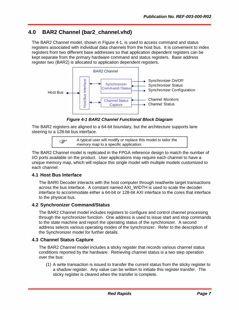
4.0 BAR2 Channel (bar2_channel.vhd)
The BAR2 Channel model, shown in Figure 4-1, is used to access command and status registers associated with individual data channels from the host bus. It is convenient to index registers from two different base addresses so that application dependent registers can be kept separate from the primary hardware command and status registers. Base address register two (BAR2) is allocated to application dependent registers.
Figure 4-1 BAR2 Channel Functional Block Diagram
The BAR2 registers are aligned to a 64-bit boundary, but the architecture supports lane steering to a 128-bit bus interface.
A typical user will modify or replace this model to tailor the memory map to a specific application.
The BAR2 Channel model is replicated in the FPGA reference design to match the number of I/O ports available on the product. User applications may require each channel to have a unique memory map, which will replace this single model with multiple models customized to each channel.
4.1 Host Bus Interface
The BAR0 Decoder interacts with the host computer through read/write target transactions across the bus interface. A constant named AXI_WIDTH is used to scale the decoder interface to accommodate either a 64-bit or 128-bit AXI interface to the cores that interface to the physical bus.
4.2 Synchronizer Command/Status
The BAR2 Channel model includes registers to configure and control channel processing through the synchronizer function. One address is used to issue start and stop commands to the state machine and report the operating status of the synchronizer. A second address selects various operating modes of the synchronizer. Refer to the description of the Synchronizer model for further details.
4.3 Channel Status Capture
The BAR2 Channel model includes a sticky register that records various channel status conditions reported by the hardware. Retrieving channel status is a two step operation over the bus:
(1) A write transaction is issued to transfer the current status from the sticky register to a shadow register. Any value can be written to initiate this register transfer. The sticky register is cleared when the transfer is complete.
Channel Monitors
BAR2 Channel
Ho
st B
us In
terf
ace
Host Bus
Channel StatusCapture
SynchronizerCommand / Status
Channel Status
Synchronizer Conf iguration
Synchronizer On/Off
Synchronizer Status
Publication No. REF-003-000-R02
Red Rapids Page 8
(2) A read transaction is issued to the shadow register to obtain the channel status.
The two step procedure is used to protect the sticky register contents from speculative read transactions that may be issued by the host operating system.
There is a separate mask register that determines whether specific channel conditions will also produce an interrupt.

Publication No. REF-003-000-R02
Red Rapids Page 9
5.0 BAR2 Common (bar2_common.vhd)
The BAR2 Common model, shown in Figure 5-1, is used to access command and status registers common to all data channels from the host bus. It is convenient to index registers from two different base addresses so that application dependent registers can be kept separate from the primary hardware command and status registers. Base address register two (BAR2) is allocated to application dependent registers.
Figure 5-1 BAR2 Common Functional Block Diagram
The BAR2 registers are aligned to a 64-bit boundary, but the architecture supports lane steering to a 128-bit bus interface.
A typical user will modify or replace this model to tailor the memory map to a specific application.
5.1 Host Bus Interface
The BAR2 Decoder interacts with the host computer through read/write target transactions across the bus interface. A constant named AXI_WIDTH is used to scale the decoder interface to accommodate either a 64-bit or 128-bit AXI interface to the cores that interface to the physical bus.
5.2 Product Identification
The BAR2 Common model includes a read-only register that conveys specific information about product features to the software application that demonstrates the reference design.
5.3 Software Trigger
Writing any value to the software trigger address will issue a single period strobe to the Synchronizer that can be used as a start/stop event. Refer to the description of the Synchronizer model for further details.
5.4 Demonstration Register
The demonstration registers illustrate the lane steering involved in reading or writing a 64-bit register on a 128-bit and 64-bit aligned address. The AXI_WIDTH constant is used to achieve proper alignment on a 64-bit aligned address. We have adopted the convention of referencing the bus range indices to (AXI_WIDTH-64) so that the additive components resemble the equivalent index for a 64-bit aligned address. For example, an address range of (63 downto 32) used on a 128-bit aligned address is expressed as ((AXI_WIDTH-64) +63 downto (AXI_WIDTH-64) +32) on a 64-bit aligned address.
BAR2 Common
Ho
st B
us In
terf
ace
Host Bus
Product
IdentificationModel Number / Features
Software
Trigger
Demonstration
Registers
Single Period Strobe
Peripheral Device CommandsPeripheral
Device Interface Peripheral Device Status

Publication No. REF-003-000-R02
Red Rapids Page 10
5.5 Peripheral Device Interface
The BAR2 Common model includes registers that exercise peripheral devices attached to the FPGA that are not connected to the primary datapath. These register are provide for demonstration purposes only and would not be needed in an actual application. The devices that are demonstrated through this interface will usually be controlled by application specific logic.
Publication No. REF-003-000-R02
Red Rapids Page 11
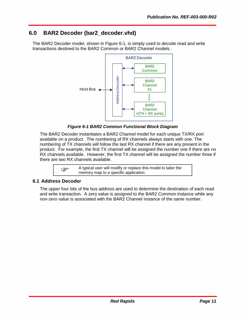
6.0 BAR2 Decoder (bar2_decoder.vhd)
The BAR2 Decoder model, shown in Figure 6-1, is simply used to decode read and write transactions destined to the BAR2 Common or BAR2 Channel models.
Figure 6-1 BAR2 Common Functional Block Diagram
The BAR2 Decoder instantiates a BAR2 Channel model for each unique TX/RX port available on a product. The numbering of RX channels always starts with one. The numbering of TX channels will follow the last RX channel if there are any present in the product. For example, the first TX channel will be assigned the number one if there are no RX channels available. However, the first TX channel will be assigned the number three if there are two RX channels available.
A typical user will modify or replace this model to tailor the memory map to a specific application.
6.1 Address Decoder
The upper four bits of the bus address are used to determine the destination of each read and write transaction. A zero value is assigned to the BAR2 Common instance while any non-zero value is associated with the BAR2 Channel instance of the same number.
BAR2 Decoder
Host Bus
BAR2Common
BAR2Channel
#1
BAR2Channel
#(TX + RX ports)
…
Ad
dre
ss D
eco
de
r

Publication No. REF-003-000-R02
Red Rapids Page 12
7.0 BPI Flash (bpi_flash.vhd & bpi_flash_stub.vhd)
The BPI Flash model, shown in Figure 7-1, allows software to program the configuration memory attached to the FPGA. A standard MCS format configuration file supplies the flash contents.
Figure 7-1 BPI Flash Functional Block Diagram
A typical user application would not change this model.
Products that are purchased with the flash hardware write protect option cannot be programmed from software. The BPI Flash stub model can be used to conserve FPGA resources if software programming is not desired or is not supported by the product. Simply replace bpi_flash.vhd with bp_flash_stub.vhd in the project.
7.1 Theory of Operation
The operation of the BPI Flash model is tightly coupled to the Flash Programmer software. The state machine is a very simple microcode engine that translates commands from software into equivalent Flash transactions. Status and read transactions return the requested information back to software through a reply channel.
BPI Flash
Flash
FIFO
MMCM (20 MHz)
State
Machine
Flash
FIFOCommand Reply

Publication No. REF-003-000-R02
Red Rapids Page 13
8.0 Clock Crossing (clock_crossing.vhd)
The Clock Crossing model is a handy utility function that passes a single trigger enable bit between two clock domains of arbitrary frequency. This function is particularly useful when a command register in the bus clock domain needs to produce a result in a channel clock domain.
A typical user application would not change this model.
8.1 Input
The Clock Crossing model will produce a valid output from a single clock period duration strobe in the source clock domain. A longer duration strobe is also allowed since the output is actually generated by the leading edge of the strobe.
8.2 Output
The Clock Crossing model produces a single clock period duration strobe in the target clock domain.
Publication No. REF-003-000-R02
Red Rapids Page 14
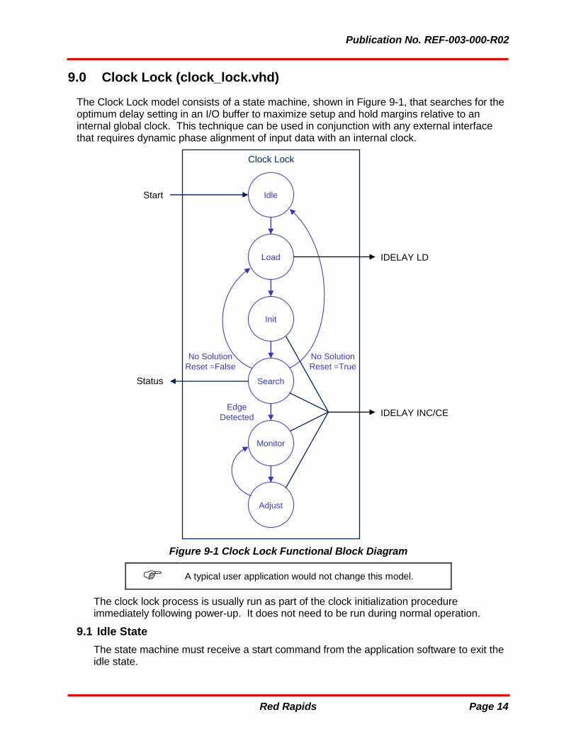
9.0 Clock Lock (clock_lock.vhd)
The Clock Lock model consists of a state machine, shown in Figure 9-1, that searches for the optimum delay setting in an I/O buffer to maximize setup and hold margins relative to an internal global clock. This technique can be used in conjunction with any external interface that requires dynamic phase alignment of input data with an internal clock.
Figure 9-1 Clock Lock Functional Block Diagram
A typical user application would not change this model.
The clock lock process is usually run as part of the clock initialization procedure immediately following power-up. It does not need to be run during normal operation.
9.1 Idle State
The state machine must receive a start command from the application software to exit the idle state.
Clock Lock
Idle
Load
Init
Search
Monitor
Start
IDELAY INC/CE
Adjust
IDELAY LD
Status
No Solution
Reset =False
Edge
Detected
No Solution
Reset =True

Publication No. REF-003-000-R02
Red Rapids Page 15
9.2 Load State
The delay element located in the I/O buffer is loaded with the tap setting defined by the IDELAY_VALUE generic. The state machine can also be instructed to perform a load if no solution is found.
9.3 Initialization State
A FIR filter is used to prevent false edge detection by removing single sample glitches from the reference input, which is usually a forwarded clock. A counter holds the state machine in the initialization state until each of the six filter taps contain valid data.
9.4 Search State
The delay element is incremented until an edge transition is found on the reference input. When an edge is detected, the state machine transitions to the monitor state to maintain optimum timing by correcting for jitter on the reference. If no solution is found, the search will either transition back to the load state and make another attempt or return to the Idle state to abandon the search. The specific action is determined by the RESET_IF_NOSOL generic logical value.
9.5 Monitor State
The timing solution is continuously monitored to correct for any deviations in the edge transition over time. This is accomplished by continuously evaluating the state of the reference input on both sides of the detected edge. The monitor state toggles the reference tap delay between the leading and trailing edge so that the adjust state can make any necessary corrections.
A reset is required to return the state machine back to Idle after it has entered the monitor state.
9.6 Adjust State
The tap delay values in the primary datapath are updated to a new value when it is determined that the edge detected on the reference input has moved. The FIR filter is again used to remove glitches that might result in an incorrect adjustment.
Publication No. REF-003-000-R02
Red Rapids Page 16
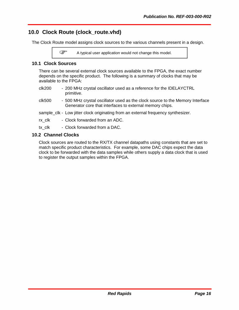
10.0 Clock Route (clock_route.vhd)
The Clock Route model assigns clock sources to the various channels present in a design.
A typical user application would not change this model.
10.1 Clock Sources
There can be several external clock sources available to the FPGA, the exact number depends on the specific product. The following is a summary of clocks that may be available to the FPGA:
clk200 - 200 MHz crystal oscillator used as a reference for the IDELAYCTRL primitive.
clk500 - 500 MHz crystal oscillator used as the clock source to the Memory Interface Generator core that interfaces to external memory chips.
sample_clk - Low jitter clock originating from an external frequency synthesizer.
rx_clk - Clock forwarded from an ADC.
tx_clk - Clock forwarded from a DAC.
10.2 Channel Clocks
Clock sources are routed to the RX/TX channel datapaths using constants that are set to match specific product characteristics. For example, some DAC chips expect the data clock to be forwarded with the data samples while others supply a data clock that is used to register the output samples within the FPGA.
Publication No. REF-003-000-R02
Red Rapids Page 17
11.0 DAC Interface (dac_interface.vhd)
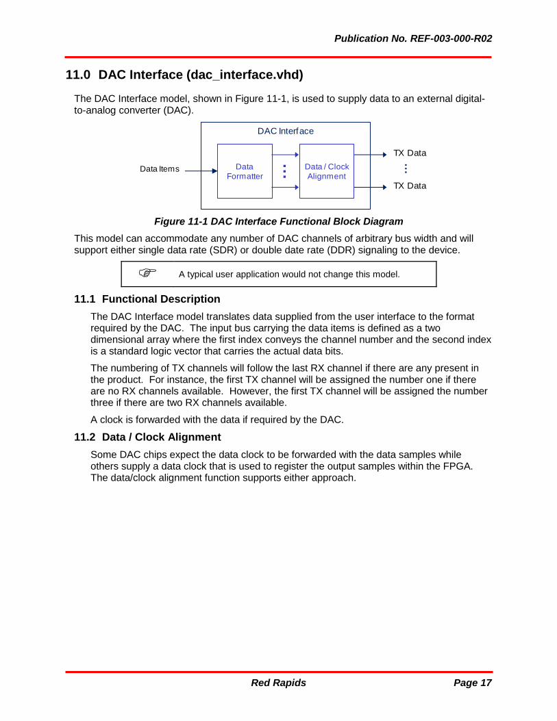
The DAC Interface model, shown in Figure 11-1, is used to supply data to an external digital-to-analog converter (DAC).
Figure 11-1 DAC Interface Functional Block Diagram
This model can accommodate any number of DAC channels of arbitrary bus width and will support either single data rate (SDR) or double date rate (DDR) signaling to the device.
A typical user application would not change this model.
11.1 Functional Description
The DAC Interface model translates data supplied from the user interface to the format required by the DAC. The input bus carrying the data items is defined as a two dimensional array where the first index conveys the channel number and the second index is a standard logic vector that carries the actual data bits.
The numbering of TX channels will follow the last RX channel if there are any present in the product. For instance, the first TX channel will be assigned the number one if there are no RX channels available. However, the first TX channel will be assigned the number three if there are two RX channels available.
A clock is forwarded with the data if required by the DAC.
11.2 Data / Clock Alignment
Some DAC chips expect the data clock to be forwarded with the data samples while others supply a data clock that is used to register the output samples within the FPGA. The data/clock alignment function supports either approach.
DAC Interface
DataFormatter …
Data Items Data / ClockAlignment
…
TX Data
TX Data
Publication No. REF-003-000-R02
Red Rapids Page 18
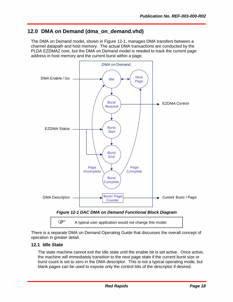
12.0 DMA on Demand (dma_on_demand.vhd)
The DMA on Demand model, shown in Figure 12-1, manages DMA transfers between a channel datapath and host memory. The actual DMA transactions are conducted by the PLDA EZDMA2 core, but the DMA on Demand model is needed to track the current page address in host memory and the current burst within a page.
Figure 12-1 DAC DMA on Demand Functional Block Diagram
A typical user application would not change this model.
There is a separate DMA on Demand Operating Guide that discusses the overall concept of operation in greater detail.
12.1 Idle State
The state machine cannot exit the idle state until the enable bit is set active. Once active, the machine will immediately transition to the next page state if the current burst size or burst count is set to zero in the DMA descriptor. This is not a typical operating mode, but blank pages can be used to expose only the control bits of the descriptor if desired.
DMA on Demand
Idle
Burst Request
Burst Start
Burst End
Burst Complete
Next Page
EZDMA Status
PageComplete
DMA Enable / Go
EZDMA Control
PageIncomplete
Burst / PageCounter
Current Burst / PageDMA Descriptor
Publication No. REF-003-000-R02
Red Rapids Page 19
If the enable is active, an active DMA Go signal from the application logic will cause a transition to the burst request state.
12.2 Burst Request
A burst request is issued to the PLDA EZDMA2 core to get a transfer started.
12.3 Burst Start
With multiple DMA channels, any request may have to wait for other transactions to complete before a burst can begin. This state monitors status from PLDA EZDMA2 core to determine when a burst starts.
12.4 Burst End
The end of a burst is also reported by the PLDA EZDMA2 core. The burst counter is incremented upon leaving this state.
12.5 Burst Complete
The burst count is checked after every burst completes to determine whether the end of the current page has been reached. If the page is complete, the machine transitions to the next page state. Otherwise, the state machine returns to idle.
12.6 Next Page
A new page address is needed under the following two circumstances:
(1) The burst size or burst count of the current descriptor is zero.
(2) The final burst of the current page has just completed.
There are 1024 possible page addresses and associated descriptors stored in FPGA memory that are loaded by the host through BAR0. The memories are indexed by a page counter within the DMA on Demand model to supply those addresses to the PLDA EZDMA2 core. Entering this state causes the page counter to increment.
12.7 Burst / Page Counter
The DMA buffers are scattered in pages throughout host memory. Each buffer assigned to a single channel can occupy up to1024 pages, but fewer pages are also allowed. Each page consists of a selectable number of bursts. The burst counter is used to determine when a page is complete so that the next burst starts at a new page address. The page counter is used to retrieve that address from memory within the FPGA.
The burst and page counters are set to zero by a hardware or software reset. They can also be set to zero when the DMA on Demand model is disabled by activating the DMA initialization control input.

Publication No. REF-003-000-R02
Red Rapids Page 20
13.0 DMA Read FIFO (dma_read_fifo.vhd)
The DMA Read FIFO model, shown in Figure 13-1, provides storage for data arriving from a DMA read request. It also provides the clock boundary crossing between the bus clock domain and the datapath clock domain.
Figure 13-1 DMA Read FIFO Functional Block Diagram
A typical user application may change this model to increase storage capacity.
A constant named AXI_WIDTH is used to scale the FIFO interface to accommodate either a 64-bit or 128-bit AXI interface to the cores that interface to the physical bus. The total storage capacity using the 128-bit AXI bus (32 kbytes) is double the capacity using a 64-bit bus (16 kbytes).
13.1 DMA FIFO
The DMA FIFO is a Xilinx primitive that receives data from the host bus interface. It supplies a data count that is used by the DMA Request function to determine when there is enough space available to satisfy a full DMA burst. The input and output ports of this FIFO both run at the bus clock frequency.
13.2 Channel FIFO
The Channel FIFO is a Xilinx primitive that bridges the clock boundary between the bus clock domain and the datapath clock domain. It transfers data from the DMA FIFO to the TX channel.
13.3 DMA Request
The DMA Read FIFO model sends a request to the DMA on Demand model anytime there is open capacity available to accept a complete DMA burst. This approach provides the widest margin to overcome DMA latency since it maximizes the number of remaining samples available to feed the datapath while waiting for the DMA to respond.
DMA Read FIFO
DMA Data ChannelFIFO
DMAFIFO
Payload Data
DMARequest
DMA Go
Publication No. REF-003-000-R02
Red Rapids Page 21
14.0 DMA Write FIFO (dma_write_fifo.vhd)
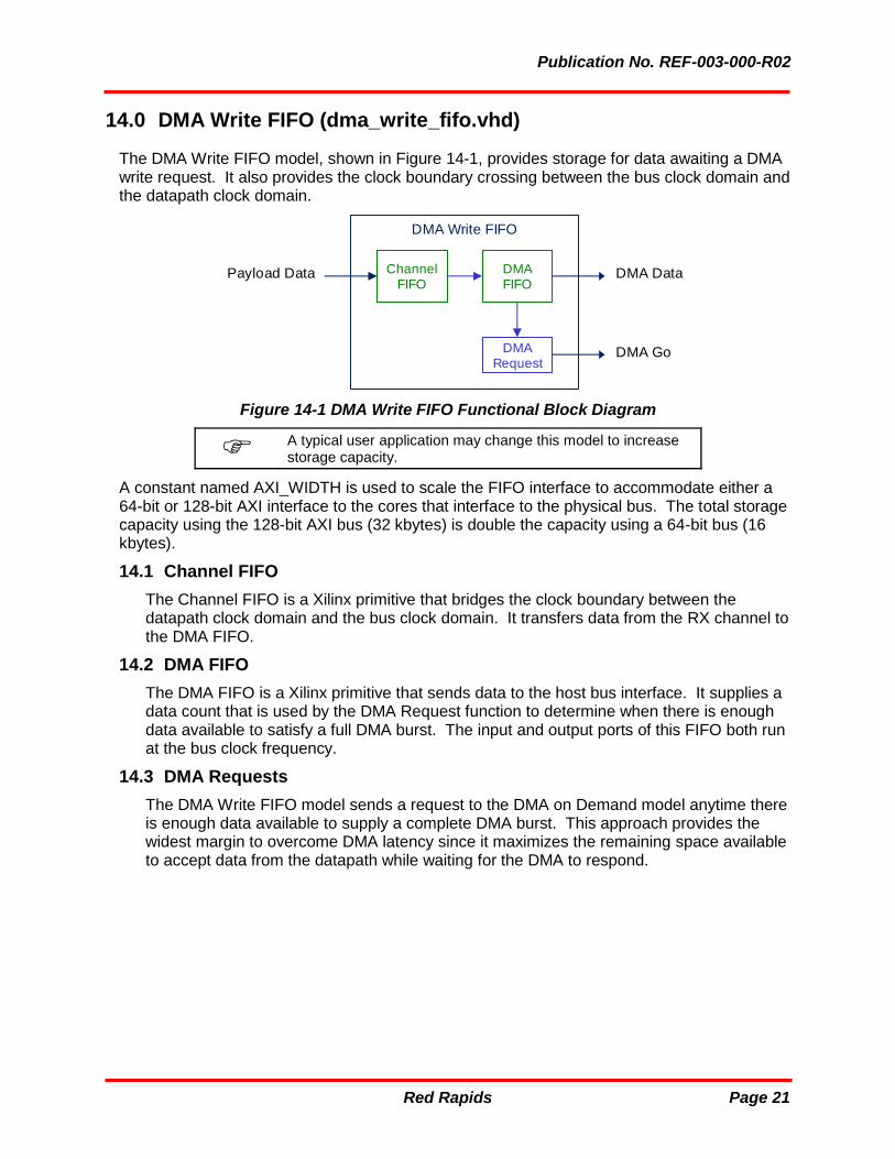
The DMA Write FIFO model, shown in Figure 14-1, provides storage for data awaiting a DMA write request. It also provides the clock boundary crossing between the bus clock domain and the datapath clock domain.
Figure 14-1 DMA Write FIFO Functional Block Diagram
A typical user application may change this model to increase storage capacity.
A constant named AXI_WIDTH is used to scale the FIFO interface to accommodate either a 64-bit or 128-bit AXI interface to the cores that interface to the physical bus. The total storage capacity using the 128-bit AXI bus (32 kbytes) is double the capacity using a 64-bit bus (16 kbytes).
14.1 Channel FIFO
The Channel FIFO is a Xilinx primitive that bridges the clock boundary between the datapath clock domain and the bus clock domain. It transfers data from the RX channel to the DMA FIFO.
14.2 DMA FIFO
The DMA FIFO is a Xilinx primitive that sends data to the host bus interface. It supplies a data count that is used by the DMA Request function to determine when there is enough data available to satisfy a full DMA burst. The input and output ports of this FIFO both run at the bus clock frequency.
14.3 DMA Requests
The DMA Write FIFO model sends a request to the DMA on Demand model anytime there is enough data available to supply a complete DMA burst. This approach provides the widest margin to overcome DMA latency since it maximizes the remaining space available to accept data from the datapath while waiting for the DMA to respond.
DMA Write FIFO
Payload Data DMAFIFO
ChannelFIFO
DMA Data
DMARequest
DMA Go

Publication No. REF-003-000-R02
Red Rapids Page 22
15.0 Interrupt Controller (interrupt_controller.vhd)
The Interrupt Controller, shown in Figure 15-1, issues an interrupt request to the host when specific error or channel status conditions exist.
Figure 15-1 Interrupt Controller Functional Block Diagram
A typical user application may change this model to add channel status events that trigger an interrupt.
15.1 Monitor
The monitors are separated into two categories; errors and channel status. The error monitors are routed to a sticky register in the BAR0 Decoder model. The channel status is routed to a sticky register in the BAR2 Channel model. Monitor bits that originate from a clock domain other than the bus clock are routed through the Clock Crossing model to ensure that an event is not missed.
15.2 Interrupt
The contents of the sticky registers in the BAR0 Decoder and BAR2 Channel models are routed back to the Interrupt Controller model for comparison to the corresponding mask bits. An active bit that is not masked will produce an interrupt request.
Interrupt Controller
Error Condition Error Monitor
Monitor
Interrupt Request
Channel Condition Channel Monitor
Interrupt
Error Status
Channel Status
Publication No. REF-003-000-R02
Red Rapids Page 23
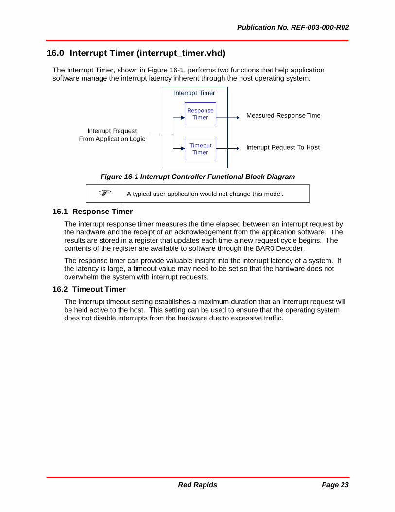
16.0 Interrupt Timer (interrupt_timer.vhd)
The Interrupt Timer, shown in Figure 16-1, performs two functions that help application software manage the interrupt latency inherent through the host operating system.
Figure 16-1 Interrupt Controller Functional Block Diagram
A typical user application would not change this model.
16.1 Response Timer
The interrupt response timer measures the time elapsed between an interrupt request by the hardware and the receipt of an acknowledgement from the application software. The results are stored in a register that updates each time a new request cycle begins. The contents of the register are available to software through the BAR0 Decoder.
The response timer can provide valuable insight into the interrupt latency of a system. If the latency is large, a timeout value may need to be set so that the hardware does not overwhelm the system with interrupt requests.
16.2 Timeout Timer
The interrupt timeout setting establishes a maximum duration that an interrupt request will be held active to the host. This setting can be used to ensure that the operating system does not disable interrupts from the hardware due to excessive traffic.
Interrupt Timer
Interrupt Request
From Application Logic
Measured Response TimeResponse
Timer
Interrupt Request To HostTimeoutTimer

Publication No. REF-003-000-R02
Red Rapids Page 24
17.0 PCI Express (pci_express.vhd)
The PCI Express model, shown in Figure 17-1, is simply a hierarchical grouping of models needed to abstract the PCIe bus to a much simpler internal bus. There are two third party cores that constitute the entire datapath. The Xilinx Integrated Block for PCI Express core performs the PCIe endpoint function and the PLDA EZDMA2 core supplies the application logic with eight master DMA channels along with a slave interface for target transactions.
Figure 17-1 PCI Express Functional Block Diagram
A typical user application may change the configuration of the PCI endpoint.
17.1 Xilinx 7 Series Integrated Block Plus for PCI Express
The 7 Series Integrated Block Plus for PCI Express is available in the Xilinx Vivado IP catalog. This core passes commands and data between the host PCIe bus and an internal AXI bus that connects to the PLDA EZDMA2 core.
The core offers a wide range of configuration variables, but there are only four that would likely be modified for a user application:
Number of Lanes - The number of electrical lanes that will connect to the host through the PCI Express socket (x1, x2, x4, x8).
Maximum Link Speed - The speed of each PCI Express lane expressed in GT/s. Gen1 = 2.5 GT/s Gen2 = 5.0 GT/s Gen3 = 8.0 GT/s
AXI Interface Frequency - Clock frequency of the AXI bus (125 MHz or 250 MHz).
AXI Interface Width - Width of the AXI bus (64 bits or 128 bits).
The number of lanes is typically dictated by the connector available on the host computer. Each connector is described in terms of a physical and electrical specification. The XMC connector has a fixed physical size and up to eight electrical lanes, the most common configurations are x4 and x8. The physical size of the PCIe connector can vary, but it is never smaller than the number of electrical lanes. For example, a x8 electrical connector may be x8 physical or x16 physical. The endpoint core should be configured for no more than the maximum number of electrical lanes provided by the socket.
PCI Express
PCITransaction
Decoder
Internal Bus
InterruptTimer
PLDAEZDMA2
PCIeEndpoint
Host PCIe Bus
Publication No. REF-003-000-R02
Red Rapids Page 25
The maximum link speed is also dictated by the connector available on the host computer. The endpoint core should be configured for the maximum performance available from the host socket. The link speed should automatically negotiate downward if the connector does not support the speed selected for the endpoint.
The AXI bus interface frequency and width should be selected to match the composite bandwidth of the PCIe interface. For example, the maximum frequency (250 MHz) and maximum width (128 bits) would be needed to match the bandwidth available from a x8 Gen2 PCIe interface. If the number of lanes is reduced to x4 or the link speed reduced to Gen1, then either the AXI frequency could be reduced to 125 MHz or the width could be reduced to 64 bits. The Xilinx IP wizard will automatically size the AXI interface to match the performance of the selected PCIe interface.
Vivado projects that are distributed with each reference design have the core configured to achieve the highest performance available to the FPGA technology. These setting can be modified by opening the IP wizard from within the Vivado project.
The remainder of this section describes the configuration settings used to produce the default PCIe endpoint core settings from the 7 Series Integrated Block Plus for PCI Express IP wizard.

Publication No. REF-003-000-R02
Red Rapids Page 26
The “Basic” configuration tab of the wizard, shown in Figure 17-2, sets the device parameters and bus performance. These options can be modified to fit the target system expected by the application. It is important to select the PLDA EZDMA2 core that matches the AXI frequency and bus width selected on this page, see section 17.2 for more details.
Figure 17-2 PCI Express IP Wizard (Basic Tab)

Publication No. REF-003-000-R02
Red Rapids Page 27
The “IDs” configuration tab establishes the PCI vendor and device identification. These settings should not be altered from what is shown in Figure 17-3.
Figure 17-3 PCI Express IP Wizard (IDs Tab)
Publication No. REF-003-000-R02
Red Rapids Page 28
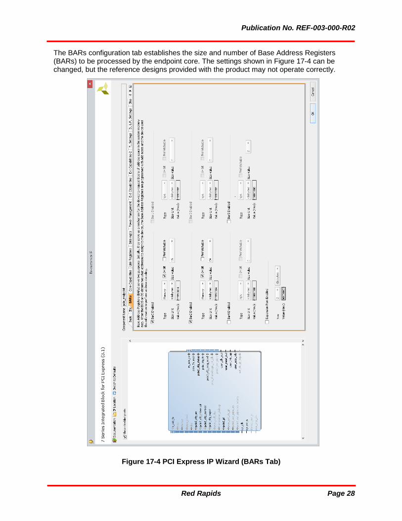
The BARs configuration tab establishes the size and number of Base Address Registers (BARs) to be processed by the endpoint core. The settings shown in Figure 17-4 can be changed, but the reference designs provided with the product may not operate correctly.
Figure 17-4 PCI Express IP Wizard (BARs Tab)

Publication No. REF-003-000-R02
Red Rapids Page 29
The Core Capabilities configuration tab settings shown in Figure 17-4 are selected to optimize performance of DMA transfers. The maximum payload size must be set to 256 bytes to match the PLDA EZDMA2 core settings, see section 17.2 for more details.
Figure 17-5 PCI Express IP Wizard (Core Capabilities Tab)

Publication No. REF-003-000-R02
Red Rapids Page 30
The Link Registers configuration tab settings shown in Figure 17-4 are left at the default values.
Figure 17-6 PCI Express IP Wizard (Link Registers Tab)

Publication No. REF-003-000-R02
Red Rapids Page 31
The Interrupts configuration tab settings shown in Figure 17-4 are set to allow the core to process message signalled interrupts.
Figure 17-7 PCI Express IP Wizard (Interrupts Tab)

Publication No. REF-003-000-R02
Red Rapids Page 32
The Power Management configuration tab settings shown in Figure 17-4 are left at the default values.
Figure 17-8 PCI Express IP Wizard (Power Management Tab)

Publication No. REF-003-000-R02
Red Rapids Page 33
The Extended Capabilities configuration tab settings shown in Figure 17-4 are left at the default values.
Figure 17-9 PCI Express IP Wizard (Extended Capabilities Tab)

Publication No. REF-003-000-R02
Red Rapids Page 34
The Extended Capabilities-2 configuration tab settings shown in Figure 17-4 are left at the default values.
Figure 17-10 PCI Express IP Wizard (Extended Capabilities-2 Tab)
Publication No. REF-003-000-R02
Red Rapids Page 35
The TL Settings configuration tab settings shown in Figure 17-4 are left at the default values.
Figure 17-11 PCI Express IP Wizard (TL Settings Tab)

Publication No. REF-003-000-R02
Red Rapids Page 36
The DL & DP Settings configuration tab settings shown in Figure 17-4 are left at the default values.
Figure 17-12 PCI Express IP Wizard (DL & DP Settings Tab)
Publication No. REF-003-000-R02
Red Rapids Page 37
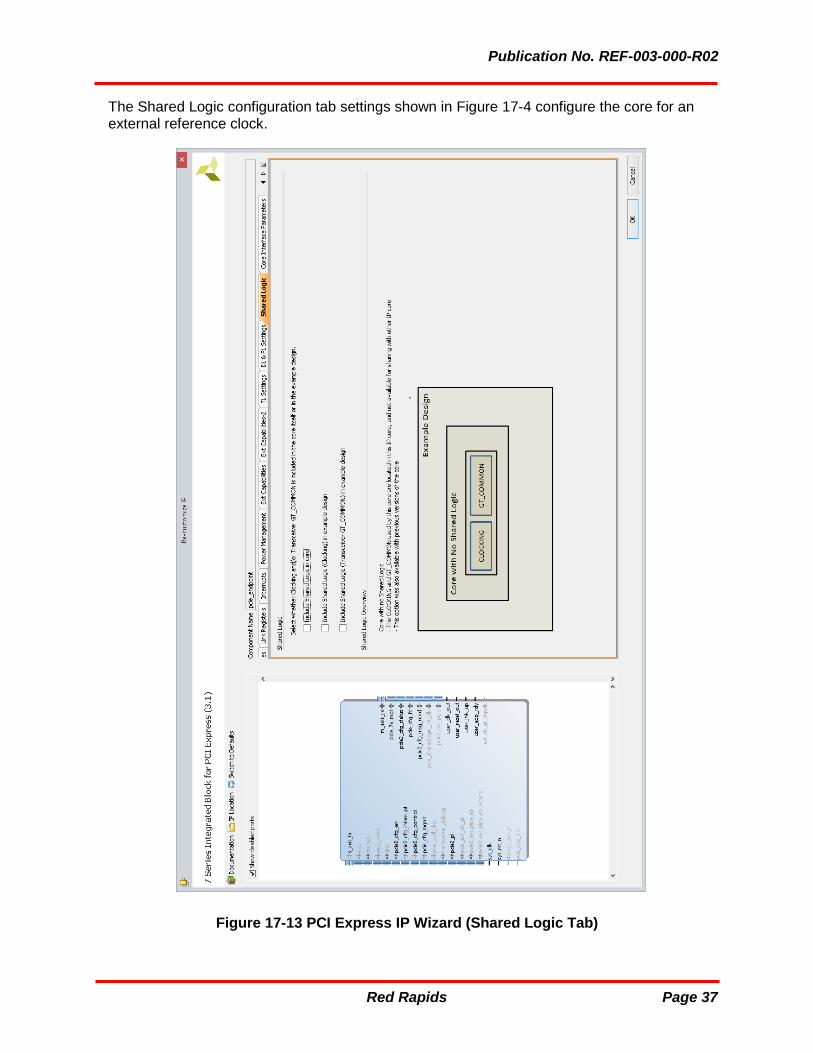
The Shared Logic configuration tab settings shown in Figure 17-4 configure the core for an external reference clock.
Figure 17-13 PCI Express IP Wizard (Shared Logic Tab)

Publication No. REF-003-000-R02
Red Rapids Page 38
The Core Interface Parameters configuration tab settings shown in Figure 17-4 are left at the default values.
Figure 17-14 PCI Express IP Wizard (Core Interface Parameters Tab)

Publication No. REF-003-000-R02
Red Rapids Page 39
17.2 PLDA EZDMA2
Reference designs supplied by Red Rapids include an EDIF netlist for the EZDMA2 core offered by IP vendor PLDA. It is not necessary to purchase a license from PLDA to use this core in the netlist form provided in the Red Rapids distribution archive. There are four different EZDMA2 netlists included in the distribution archive for compatibility with the four AXI bus configuration options available in the Xilinx 7 Series Integrated Block Plus for PCI Express core:
AXI Frequency AXI Width
125 MHz 64 bits
125 MHz 128 bits
250 MHz 64 bits
250 MHz 128 bits
The projects distributed with a reference design default to the highest performance configuration available to the FPGA technology. Alternate configurations can be loaded by simply substituting the IP files from another directory on the distribution archive.
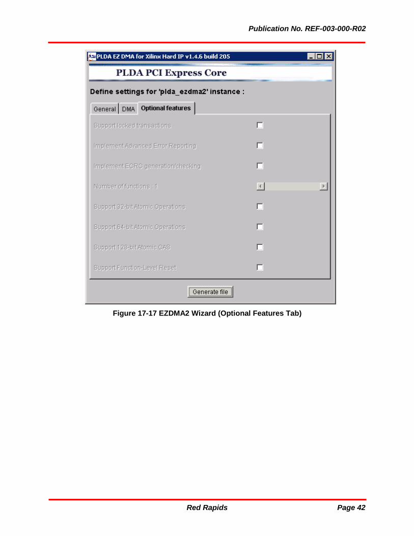
The screen captures shown in Figure 17-15 through Figure 17-17 display the specific wizard settings used to produce the EZDMA2 netlist for a 128-bit AXI bus clocked at 250 MHz. The default settings can only be changed by requesting a custom netlist from Red Rapids or purchasing a core license from PLDA.
Documentation for the EZDMA2 core is available on the PLDA website (www.plda.com).

Publication No. REF-003-000-R02
Red Rapids Page 40
Figure 17-15 EZDMA2 Wizard (General Tab)

Publication No. REF-003-000-R02
Red Rapids Page 41
Figure 17-16 EZDMA2 Wizard (DMA Tab)
Publication No. REF-003-000-R02
Red Rapids Page 42
Figure 17-17 EZDMA2 Wizard (Optional Features Tab)

Publication No. REF-003-000-R02
Red Rapids Page 43
18.0 PCI Performance (pci_performance.vhd)
The PCI Performance model, shown in Figure 18-1, measures the actual DMA throughput and latency achieved by the FPGA operating in the host environment.
Figure 18-1 PCI Performance Functional Block Diagram
A typical user application would eliminate this model from the design unless continuous performance monitoring provides some benefit.
18.1 DMA Throughput Measurement
The DMA throughput is measured by counting TX and RX transactions over a quarter second interval. The measured values do not necessarily reflect the maximum attainable performance, they simply report activity over the most recent quarter second period. The process runs continuously, so there is a new update every quarter second.
The demonstration software measures the maximum sustained throughput by continuously requesting DMA transfers over the quarter second measurement period.
18.2 DMA Latency Measurement
DMA latency is a measurement of the time taken by the host computer to respond to a TX or RX DMA request generated by the FPGA. A register stores the highest TX and RX values recorded until a command is issued to clear the results. The process runs continuously, so the measurement can span very long operating intervals.
PCI Performance
Quarter Second
Counter
DMA
Throughput
Measurement
RX Transaction
Counter
TX Transaction
Counter
RX Latency
CounterDMA
Latency
MeasurementTX Latency
Counter
RX Latency
(4ns counts)
TX Latency
(4ns counts)
RX Throughput
(bytes/sec)
TX Throughput
(bytes/sec)

Publication No. REF-003-000-R02
Red Rapids Page 44
19.0 PCI Transaction Decoder (pci_transaction_decoder.vhd)
The PCI Transaction Decoder, shown in Figure 19-1, routes all bus transactions between the PLDA EZDMA2 core and the application logic.
Figure 19-1 PCI Transaction Decoder Functional Block Diagram
A typical user application would not change this model.
19.1 Target Transactions
Target bus transactions consist of register read or write operations to an address within the memory map of a specific base address register (BAR) index. The PCI Transaction Decoder produces flags that indicate an active BAR0 or BAR2 write operation initiated by the PLDA EZDMA2 core. A target read operation produces a read completion DMA. The PCI Transaction Decoder supplies the necessary descriptors to the PLDA EZDMA2 core to perform the read completion.
19.2 DMA Transactions
There is a single bus into the PLDA EZDMA2 core that handles all data traffic associated with a DMA write transaction. The PCI Transaction Decoder routes the appropriate data source to this bus based on select bits from the PLDA EZDMA2 core.
PCI Transaction
Decoder
BAR0 SelectTarget
TransactionsTarget Read / Write
BAR2 Select
DMATransactions
Channel #1 Data
Channel #7 Data
BAR0 / BAR2 Read
…
DMA Read Data
Publication No. REF-003-000-R02
Red Rapids Page 45
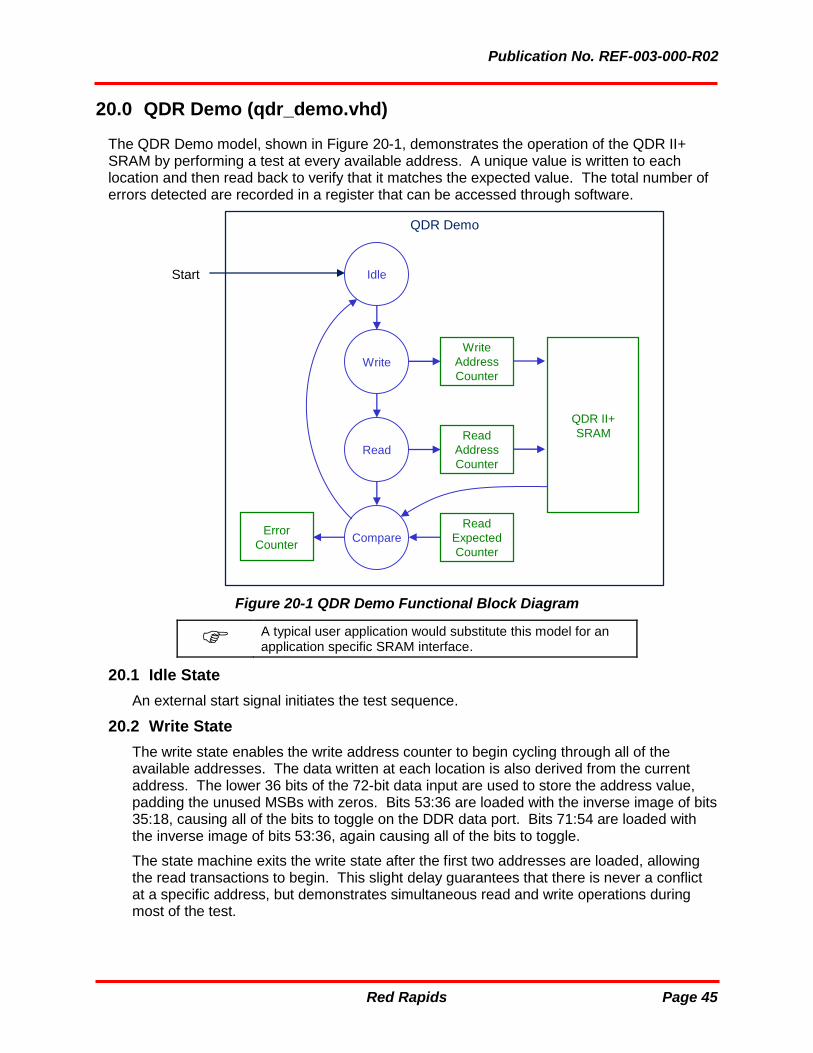
20.0 QDR Demo (qdr_demo.vhd)
The QDR Demo model, shown in Figure 20-1, demonstrates the operation of the QDR II+ SRAM by performing a test at every available address. A unique value is written to each location and then read back to verify that it matches the expected value. The total number of errors detected are recorded in a register that can be accessed through software.
Figure 20-1 QDR Demo Functional Block Diagram
A typical user application would substitute this model for an application specific SRAM interface.
20.1 Idle State
An external start signal initiates the test sequence.
20.2 Write State
The write state enables the write address counter to begin cycling through all of the available addresses. The data written at each location is also derived from the current address. The lower 36 bits of the 72-bit data input are used to store the address value, padding the unused MSBs with zeros. Bits 53:36 are loaded with the inverse image of bits 35:18, causing all of the bits to toggle on the DDR data port. Bits 71:54 are loaded with the inverse image of bits 53:36, again causing all of the bits to toggle.
The state machine exits the write state after the first two addresses are loaded, allowing the read transactions to begin. This slight delay guarantees that there is never a conflict at a specific address, but demonstrates simultaneous read and write operations during most of the test.
QDR Demo
Idle
Write
Read
Compare
Start
QDR II+
SRAM
Write
Address
Counter
Read
Address
Counter
Read
Expected
Counter
Error
Counter

Publication No. REF-003-000-R02
Red Rapids Page 46
20.3 Read State
The read state enables the read address counter to begin cycling through all of the available addresses. The state machine exits this state after just one clock cycle to immediately begin comparing values returned from the SRAM.
20.4 Compare State
The compare state monitors values returned from the SRAM read port and compares them to the expected value that is supplied by the read expected counter. Any errors detected are logged in the error counter that can be read from software.
The state machine returns to idle after every available address has been compared.

Publication No. REF-003-000-R02
Red Rapids Page 47
21.0 QDR DLL (qdr_dll.vhd)
The QDR DLL model, shown in Figure 21-1, performs the steps necessary to ensure that the DLL internal to the SRAM is properly locked to the input clock.
Figure 21-1 QDR DLL Functional Block Diagram
A typical user application would not change this model.
21.1 Idle State
The state machine remains idle during normal SRAM operation. A DLL reset procedure needs to be performed after power-on reset or if the application exerts external control to switch the DLL on after it was commanded off. The IDELAYCTRL must be stable before starting the DLL reset state machine.
21.2 Initialize State
The stable state is nothing more than a timer that counts down the interval required for the SRAM input clock to remain stable before the internal DLL is reset. The timer value is extracted from the SRAM datasheet.
QDR DLL
Idle
Stable
Reset
Settle
Done
Start
Reset
Done

Publication No. REF-003-000-R02
Red Rapids Page 48
21.3 Reset State
A hardware reset to the SRAM DLL is issued during the reset state
21.4 Settle State
The settle state is another timer that counts the number of SRAM clock cycles needed for the internal DLL to lock. The clock cycle count is extracted from the SRAM datasheet.
21.5 Done State
The done state produces a flag to the QDR SRAM model that indicates that the DLL reset procedure is complete.

Publication No. REF-003-000-R02
Red Rapids Page 49
22.0 QDR SRAM (qdr_sram.vhd & qdr_sram_stub.vhd)
The QDR SRAM model, shown in Figure 22-1, simplifies the interface to external memory by managing all of the critical timing. Each model connects to only one QDR II+ SRAM chip. Multiple instantiations are needed in a design that has access to more than one SRAM chip on the product. Memories that are not used in a design should be connected to the QDR SRAM stub model. Simply replace qdr_sram.vhd with qdr_sram_stub.vhd in the project.
Figure 22-1 QDR SRAM Functional Block Diagram
The architecture of the SRAM is presented to the application logic as a single data rate 72-bit dual-port memory instead of the more complicated 18-bit, quad data rate, burst of four structure of the actual device. There is no loss of memory bandwidth through the core by making this translation.
The read and write ports operate independently; each has a dedicated clock, data bus, and control flow. The read and write clocks can be set to any frequency. The FIFOs manage the clock domain crossing.
A typical user application would not change this model.
QDR SRAM
Write Clock
Write
Transaction
State
Machine
SRAM Write DataQDR
FIFO
Byte Write
Write Command
Write Address
Write Data
Write Ready
Busy
Dynamic
Phase
Alignment
Clock LockStart
Read Clock
SRAM Read Data
QDR
FIFO
Read Valid
Read Command
Read Address
Read Data
Read Ready
Read Acknowledge
QDR DLL
Read
Transaction
State
Machine
QDR
State Machine
Static
Phase
Alignment
SRAM Controls
QDR
FIFO
Publication No. REF-003-000-R02
Red Rapids Page 50
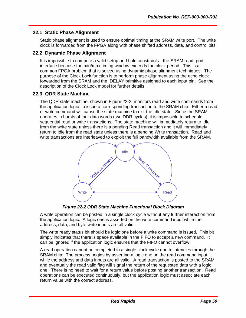
22.1 Static Phase Alignment
Static phase alignment is used to ensure optimal timing at the SRAM write port. The write clock is forwarded from the FPGA along with phase shifted address, data, and control bits.
22.2 Dynamic Phase Alignment
It is impossible to compute a valid setup and hold constraint at the SRAM read port interface because the min/max timing window exceeds the clock period. This is a common FPGA problem that is solved using dynamic phase alignment techniques. The purpose of the Clock Lock function is to perform phase alignment using the echo clock forwarded from the SRAM and the IDELAY primitive assigned to each input pin. See the description of the Clock Lock model for further details.
22.3 QDR State Machine
The QDR state machine, shown in Figure 22-2, monitors read and write commands from the application logic to issue a corresponding transaction to the SRAM chip. Either a read or write command will cause the state machine to exit the Idle state. Since the SRAM operates in bursts of four data words (two DDR cycles), it is impossible to schedule sequential read or write transactions. The state machine will immediately return to Idle from the write state unless there is a pending Read transaction and it will immediately return to idle from the read state unless there is a pending Write transaction. Read and write transactions are interleaved to exploit the full bandwidth available from the SRAM.
Figure 22-2 QDR State Machine Functional Block Diagram
A write operation can be posted in a single clock cycle without any further interaction from the application logic. A logic one is asserted on the write command input while the address, data, and byte write inputs are all valid.
The write ready status bit should be logic one before a write command is issued. This bit simply indicates that there is space available in the FIFO to accept a new command. It can be ignored if the application logic ensures that the FIFO cannot overflow.
A read operation cannot be completed in a single clock cycle due to latencies through the SRAM chip. The process begins by asserting a logic one on the read command input while the address and data inputs are all valid. A read transaction is posted to the SRAM and eventually the read valid flag will signal the return of the requested data with a logic one. There is no need to wait for a return value before posting another transaction. Read operations can be executed continuously, but the application logic must associate each return value with the correct address.
Idle
ReadWrite
Publication No. REF-003-000-R02
Red Rapids Page 51
The read ready status bit should be logic one before a read command is issued. This bit simply indicates that there is space available in the FIFO to accept a new command. It can be ignored if the application logic ensures that the FIFO cannot overflow. A logic one must be applied to the read acknowledge input to advance data through the return FIFO. The read valid output and read acknowledge input can be tied together if the application logic retrieves the return data value in a single clock cycle.
22.4 Write Transaction State Machine
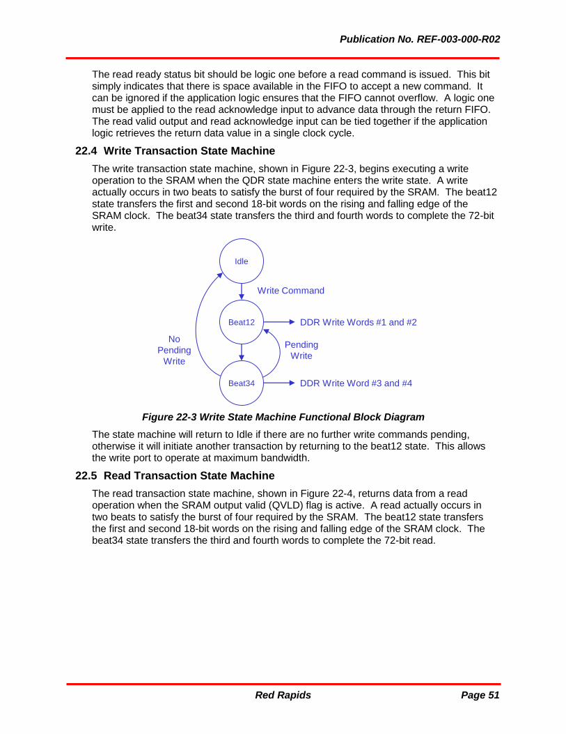
The write transaction state machine, shown in Figure 22-3, begins executing a write operation to the SRAM when the QDR state machine enters the write state. A write actually occurs in two beats to satisfy the burst of four required by the SRAM. The beat12 state transfers the first and second 18-bit words on the rising and falling edge of the SRAM clock. The beat34 state transfers the third and fourth words to complete the 72-bit write.
Figure 22-3 Write State Machine Functional Block Diagram
The state machine will return to Idle if there are no further write commands pending, otherwise it will initiate another transaction by returning to the beat12 state. This allows the write port to operate at maximum bandwidth.
22.5 Read Transaction State Machine
The read transaction state machine, shown in Figure 22-4, returns data from a read operation when the SRAM output valid (QVLD) flag is active. A read actually occurs in two beats to satisfy the burst of four required by the SRAM. The beat12 state transfers the first and second 18-bit words on the rising and falling edge of the SRAM clock. The beat34 state transfers the third and fourth words to complete the 72-bit read.
Idle
Beat12
Beat34
Write Command
DDR Write Words #1 and #2
DDR Write Word #3 and #4
Pending
Write
No
Pending
Write
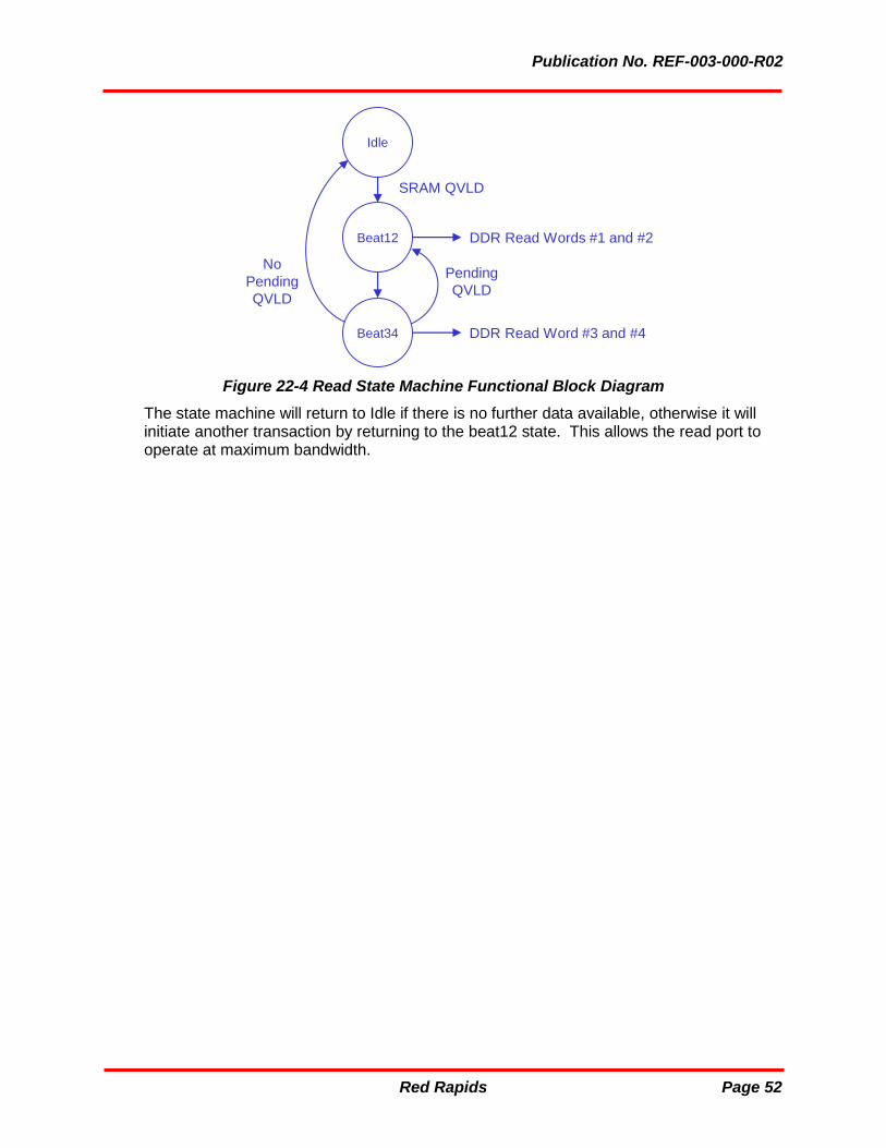
Publication No. REF-003-000-R02
Red Rapids Page 52
Figure 22-4 Read State Machine Functional Block Diagram
The state machine will return to Idle if there is no further data available, otherwise it will initiate another transaction by returning to the beat12 state. This allows the read port to operate at maximum bandwidth.
Idle
Beat12
Beat34
SRAM QVLD
DDR Read Words #1 and #2
DDR Read Word #3 and #4
Pending
QVLD
No
Pending
QVLD

Publication No. REF-003-000-R02
Red Rapids Page 53
23.0 RX Datapath (rx_datapath.vhd)
The RX Datapath, shown in Figure 23-1, is simply a hierarchical grouping of models needed to implement a complete receiver channel.
Figure 23-1 RX Datapath Functional Block Diagram
A typical user application would modify this model to add application specific functions.
RX Datapath
Data ItemsDMAWriteFIFO
RXFlow
Control
DMA Data
DMAon
DemandSynchronizerStart / Stop
DMA Address
DMA Descriptor
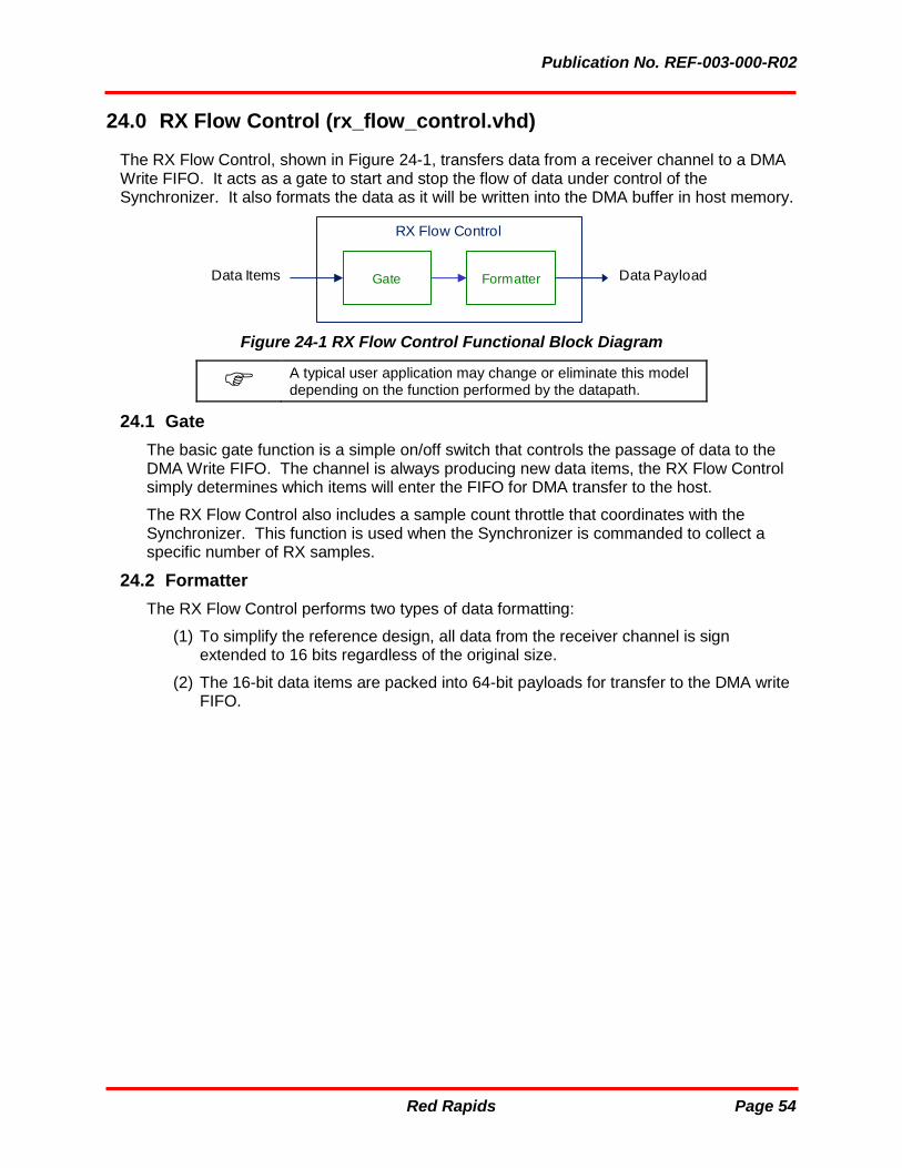
Publication No. REF-003-000-R02
Red Rapids Page 54
24.0 RX Flow Control (rx_flow_control.vhd)
The RX Flow Control, shown in Figure 24-1, transfers data from a receiver channel to a DMA Write FIFO. It acts as a gate to start and stop the flow of data under control of the Synchronizer. It also formats the data as it will be written into the DMA buffer in host memory.
Figure 24-1 RX Flow Control Functional Block Diagram
A typical user application may change or eliminate this model depending on the function performed by the datapath.
24.1 Gate
The basic gate function is a simple on/off switch that controls the passage of data to the DMA Write FIFO. The channel is always producing new data items, the RX Flow Control simply determines which items will enter the FIFO for DMA transfer to the host.
The RX Flow Control also includes a sample count throttle that coordinates with the Synchronizer. This function is used when the Synchronizer is commanded to collect a specific number of RX samples.
24.2 Formatter
The RX Flow Control performs two types of data formatting:
(1) To simplify the reference design, all data from the receiver channel is sign extended to 16 bits regardless of the original size.
(2) The 16-bit data items are packed into 64-bit payloads for transfer to the DMA write FIFO.
RX Flow Control
Data Items FormatterGate Data Payload

Publication No. REF-003-000-R02
Red Rapids Page 55
25.0 Serial Bus (serial_bus.vhd)
Many devices attached to the FPGA include a serial configuration port to communicate with internal registers. The most popular protocols are the Serial Peripheral Interface (SPI) bus and Inter-Integrated Circuit (I2C) bus, though custom formats also exist. The Serial Bus model, shown in Figure 25-1, manages all of the serial interfaces connected to the FPGA.
Figure 25-1 Serial Functional Block Diagram
A typical user application would not change this model.
25.1 Clock Divider
The serial clock is created by dividing the bus clock by 4096. This limits the highest frequency to less than 100 kHz. Many of the attached devices can accept a much higher frequency, but this value was selected to conform with the original I2C specification.
25.2 Serial Data
Serial data can be exchanged with a device over a single bidirectional connection or dedicated read and write interconnects. The data payload length can be selected in byte size increments up to a maximum length of 64 bits.
25.3 Protocol
The Serial model supports the SPI and I2C protocols used by most devices. It also interfaces to a commercial serial shift register that can be used as a simple port expander.
Serial Bus
Serial ClockClockDivider
Bus Clock
SerialData
Serial Data SPI / I2C / Custom Bus
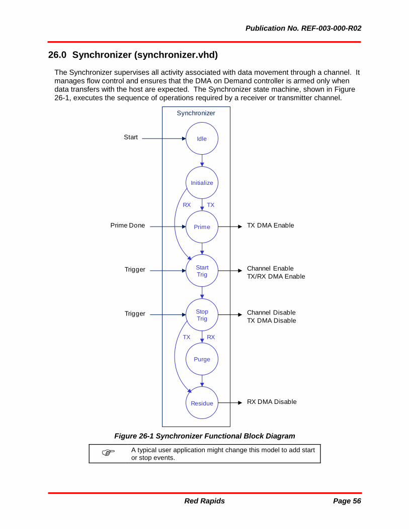
Publication No. REF-003-000-R02
Red Rapids Page 56
26.0 Synchronizer (synchronizer.vhd)
The Synchronizer supervises all activity associated with data movement through a channel. It manages flow control and ensures that the DMA on Demand controller is armed only when data transfers with the host are expected. The Synchronizer state machine, shown in Figure 26-1, executes the sequence of operations required by a receiver or transmitter channel.
Figure 26-1 Synchronizer Functional Block Diagram
A typical user application might change this model to add start or stop events.
Synchronizer
Idle
Initialize
Prime
Start Trig
Stop Trig
Purge
Residue
TXRX
TX DMA EnablePrime Done
Channel Enable
TX/RX DMA Enable
Channel Disable
TX DMA Disable
RXTX
RX DMA Disable
Start
Trigger
Trigger

Publication No. REF-003-000-R02
Red Rapids Page 57
26.1 Idle State
All channel processing is suspended while the Synchronizer is in the idle state. The DMA traffic is also disabled, any request from the channel is ignored. The Synchronizer must receive a command from the application software to exit the idle state.
26.2 Initialize State
The initialize state simply allows time for the FIFO and DMA on Demand controller to become ready after exiting reset.
26.3 Prime State
The prime state is used to preload the FIFO of a transmitter channel before the DAC is allowed to begin extracting samples. The FIFO is primed by allowing the DMA on Demand function to transfer data from the host before channel processing is enabled. Receiver channels skip the prime state.
26.4 Start Trig State
There are three different events that can be selected to initiate channel processing:
(1) None: Start the channel immediately, don’t wait for any trigger.
(2) Software Trigger: Start the channel on the active edge of the software trigger.
(3) Hardware Trigger: Start the channel on the active edge of the hardware trigger.
The start process can also be aborted by turning off the synchronizer. This feature is useful if an expected external trigger never arrives.
26.5 Stop Trig State
There are four different events that can be selected to terminate channel processing:
(1) Off Command: Stop the channel immediately.
(2) Software Trigger: Stop the channel on the active edge of the software trigger.
(3) Hardware Trigger: Stop the channel on the active edge of the hardware trigger.
(4) Sample Count: Stop the channel after the specified number of samples are processed.
26.6 Purge State
The purge state allows a receiver pipeline to finish loading the FIFO after channel processing is disabled. This is done to ensure that any samples in transition from the ADC to the FIFO can contribute to a potential final DMA transfer to the host. Transmitter channels skip the purge state.
26.7 Residue State
It is very important that the application software does not release the protected memory allocated to DMA buffers while a transaction is in progress. The residue state ensures that all DMA activity has been completed before the Synchronizer state machine returns to idle, which is the indication to software that the buffers can be released.
The residue state simply waits for a potential active DMA burst to complete on a transmit channel. The data from that burst will not be consumed by the DAC and there is no danger of any further DMA activity because traffic is disabled.

Publication No. REF-003-000-R02
Red Rapids Page 58
The residue state is used to drain the FIFO of a receiver channel after the last sample has been collected. The FIFO is purged by allowing the DMA on Demand function to continue transferring data to the host after channel processing is disabled.
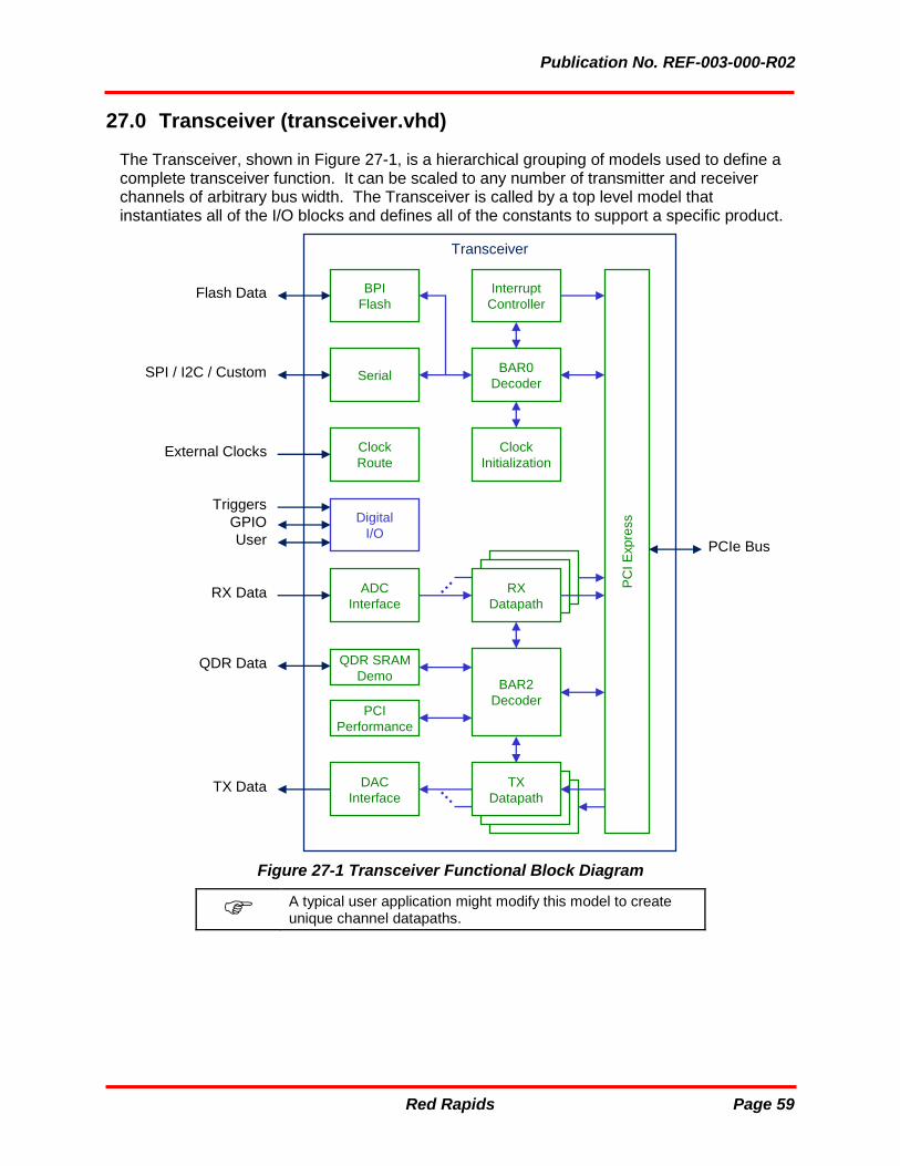
Publication No. REF-003-000-R02
Red Rapids Page 59
27.0 Transceiver (transceiver.vhd)
The Transceiver, shown in Figure 27-1, is a hierarchical grouping of models used to define a complete transceiver function. It can be scaled to any number of transmitter and receiver channels of arbitrary bus width. The Transceiver is called by a top level model that instantiates all of the I/O blocks and defines all of the constants to support a specific product.
Figure 27-1 Transceiver Functional Block Diagram
A typical user application might modify this model to create unique channel datapaths.
RX
Datapath
Transceiver
RX Data ADC
Interface
Serial
PC
I E
xp
ress
PCIe Bus
DAC
Interface
BAR0
Decoder
BAR2
Decoder
Clock
Initialization
Clock
Route
Interrupt
Controller
BPI
Flash
SPI / I2C / Custom
TX Data
External Clocks
Flash Data
QDR SRAM
DemoQDR Data
TX
Datapath
RX
DatapathRX
Datapath
TX
Datapath
TX
Datapath
Digital
I/OGPIO
Triggers
User
PCI
Performance
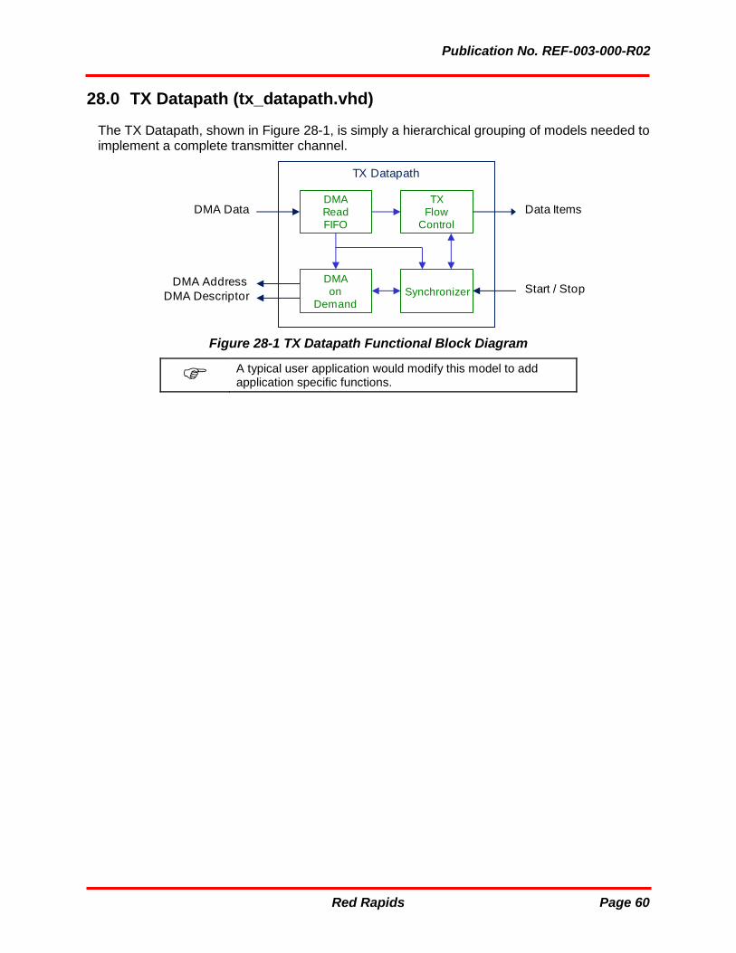
Publication No. REF-003-000-R02
Red Rapids Page 60
28.0 TX Datapath (tx_datapath.vhd)
The TX Datapath, shown in Figure 28-1, is simply a hierarchical grouping of models needed to implement a complete transmitter channel.
Figure 28-1 TX Datapath Functional Block Diagram
A typical user application would modify this model to add application specific functions.
TX Datapath
DMA DataDMAReadFIFO
TXFlow
Control
Data Items
DMAon
DemandSynchronizer Start / Stop
DMA Address
DMA Descriptor

Publication No. REF-003-000-R02
Red Rapids Page 61
29.0 TX Flow Control (tx_flow_control.vhd)
The TX Flow Control, shown in Figure 29-1, transfers data from a DMA Read FIFO to a transmitter channel. It acts as a gate to start and stop the flow of data under control of the Synchronizer. It also extracts the data items from the payload format retrieved from the DMA buffer in host memory.
Figure 29-1 TX Flow Control Functional Block Diagram
A typical user application may change or eliminate this model depending on the function performed by the datapath.
29.1 Gate
The basic gate function is a simple on/off switch that controls the passage of data to the channel. The channel is always consuming new data items, the RX Flow Control simply feeds zero value data items to the channel when the gate is off.
The TX Flow Control also includes a sample count throttle that coordinates with the Synchronizer. This function is used when the Synchronizer is commanded to transmit a specific number of TX samples.
29.2 Formatter
The TX Flow Control performs two types of data formatting:
(1) The 64-bit data payloads extracted from the DMA Read FIFO are stripped into 16-bit data items regardless of the size needed by the channel.
(2) The 16-bit data items are truncated to the size expected by the channel.
TX Flow Control
Data ItemsFormatter GateData Payload