vertically aligned carbon nanotubes embedded in … library/research/coal/cross-cutting... ·...
TRANSCRIPT

Vertically Aligned Carbon Nanotubes Embedded in Ceramic Matrices for Hot Electrode Applications

This image cannot currently be displayed.This image cannot currently be displayed.
I. Goal and Objectives
II. Background and Motivations
III. Proposed Activities 1. Super growth of vertically aligned carbon nanotube (VA-CNT) carpets 2. Fabrication of CNT-boron nitride (CNT-BN) composite structures 3. Stability and resistance studies of the CNT-BN composite structures 4. Thermionic emissions of the CNT-BN composite structures
IV. Deliverables and Spending Plan
V. Student Training
VI. Preliminary Results
Outline

This image cannot currently be displayed.This image cannot currently be displayed.
I - Goal and Objectives Primary goal: Develop CNT-BN composite structures in which VA-CNTs are
embedded in BN matrices for hot electrode applications in magnetohydrodynamics (MHD) power systems.
Objectives: 1. Super growth of VA-CNT carpets
2. Fabrication of CNT-BN composite structures
3. Stability and resistance studies of the CNT-BN composite structures
4. Thermionic emissions from the CNT-BN composite structures

This image cannot currently be displayed.This image cannot currently be displayed.
II - Background and Motivations
How to address?
New Energy Sources High Energy Efficiency

This image cannot currently be displayed.This image cannot currently be displayed.
II - Background and Motivations
Electricity Generation Efficiency Method Efficiency (%) Ref. Nuclear 33 – 36 Efficiency in Electricity Generation, EURELECTRIC
“Preservation of Resources” Working Group’s “Upstream” Sub-Group in collaboration with VGB, 2003 Coal 39 - 47
Natural gas < 39
http://crf.sandia.gov/index.php/coal-use-and-carbon-capture-technologies/#.VBaDbvldV8E
http://www.eia.gov/tools/faqs/faq.cfm?id=427&t=3
Coal 39%
Natural Gas 27%
Nuclear 19%
Hydroelectric 7%
Other renewable 6% Liquid petroleum 2%
U.S. Electricity Generation (2013)

This image cannot currently be displayed.This image cannot currently be displayed.
II - Background and Motivations
1) Only working fluid is circulated without moving mechanical parts; 2) The ability to reach full power level almost directly. 3) Lower infrastructure cost than conventional generators. 4) A very high efficiency (60% for a closed cycle MHD). http://en.wikipedia.org/wiki/Magnetohydrodynamic_generator#Generator_efficiency

This image cannot currently be displayed.This image cannot currently be displayed.
II - Background and Motivations Material Challenges for a MHD Generator
Requirement Remarks Electrical conductivity (σ) σ > 1 S/m, flux ≈ 1 amp/cm2
Thermal conductivity (k) High heat flux from the combustion fluids at 2400 K
Thermal stability Melting point (Tm) above 2400 K
Oxidation resistance Resistant to an oxygen partial pressure about 10-2 atm at
2400 K
Corrosion resistance Potassium seeds and aluminosilicate slags
Erosion resistance High velocity hot gases and particulates
Thermionic emission The anode and cathode should be good acceptor and
emitters, respectively.

This image cannot currently be displayed.This image cannot currently be displayed.
III - Proposed Solution and Activities
Tasks Milestone Completion Date
1.Project Management and Planning
Complete of the proposed project within the 3-year period.
08/31/2017
2.Super Growth of Vertically Aligned CNT Carpets
Achieve the growth of VA-CNT carpets on Cu substrates with CNT lengths up to 1 cm.
08/31/2015
3.Fabrication of CNT-BN Composite Structures
Achieve uniform and dense growth of BN matrices wrapping VA-CNTs.
02/29/2016
4.Stability and Resistance studies of the CNT-BN Composite Structures
Determine the stability and resistance of the CNT-BN composite structures
08/31/2016
Determine the electrical and thermal conductivities of the CNT-BN composite structures.
02/28/2017
5.Thermionic emissions from the CNT-BN composite structures
Determine the thermionic emission performance of the CNT-BN composite structures.
08/31/2017
Project tasks, milestones, and planned completion dates

This image cannot currently be displayed.This image cannot currently be displayed.
III - Proposed Solution and Activities Timelines and corresponding milestones of the project

This image cannot currently be displayed.This image cannot currently be displayed.
IV - Deliverables and Spending Plan
Type Deliverables Method 1. Super-growth of ultralong VA-CNT carpets
2. Fabrication of CNT-BN composite 3. Modulated photothermal radiometric method for measuring
the thermal conductivity of the CNT-BN composite 4. Thermionic emission current method for measuring the
thermionic emission of the CNT-BN composite Equipment
setup 1. Water-vapor-assisted CVD system 2. Plasma-enhanced CVD system 3. Modulated photothermal radiometric system 4. Thermionic emission current measurement system
Reports Quarterly reports, annual reports, final report and other reports required by DOE
Presentations Conference and review meeting presentations Journal papers Journal and conference proceeding articles

This image cannot currently be displayed.This image cannot currently be displayed.
V - Student Training Name Qiming Zou Degree Ph.D.
Dept. Electrical Engineering Univ. University of Nebraska - Lincoln
Goal Pursuing a Ph.D. degree in the field of Electrical Engineering and developing necessary knowledge, expertise, leadership, teaching skills, and mentorship towards an academic profession.
Objectives 1. Grasping necessary knowledge in the field of electrical engineering; 2. Grasping necessary experimental and simulation techniques required in this
project; 3. Establishing teaching skills by taking two semester teaching assistants and
participating in outreach programs; 4. Developing leadership and mentorship by working with undergraduate assistant,
Joseph Hartwig; 5. Publishing at least 3 articles in peer-reviewed journals within related fields; 6. Developing essential communication skills; 7. Attending academic conferences within related fields and establishing
networking capability; and 8. Independent and critical thinking by developing a complete research plan in his
comprehensive exam.

This image cannot currently be displayed.This image cannot currently be displayed.
V - Student Training Name Joseph Hartwig Degree B.Sc.
Dept. Electrical Engineering Univ. University of Nebraska - Lincoln
Goal Completing a B.Sc. program in the field of Electrical Engineering and obtaining essential knowledge, skills, and industrial experience for pursuing a related profession.
Objectives 1. Grasping necessary knowledge in the field of electrical engineering; 2. Grasping necessary experimental and simulation techniques required in this
project; 3. Establishing essential industrial experience by conducting industrial intership; 4. Developing effective communication skills; and 5. Developing collaborative and teamwork skills.

This image cannot currently be displayed.This image cannot currently be displayed.
VI - Preliminary Results
1. Growing CNTs with alignment control
2. Optically controlled in situ growth and parallel integration of CNTs
3. Direct formation of graphene on dielectric surfaces via a solid-state process
4. Laser direct writing of graphene patterns
5. Resonant vibrational excitation in diamond growth control
6. Low-temperature synthesis of GaN thin films

This image cannot currently be displayed.This image cannot currently be displayed.
VI - Preliminary Results
1. Growing CNTs with alignment control
Ref.: Applied Physics Letters, 2009, 95(14), 143117.

This image cannot currently be displayed.This image cannot currently be displayed.
VI - Preliminary Results
1. Growing CNTs with alignment control
Vertically aligned CNT patterns

This image cannot currently be displayed.This image cannot currently be displayed.
VI - Preliminary Results
2. Optically controlled in situ growth and parallel integration of CNTs
Top view Side view
Ref.: Nanotechnology. 2010, 21, 315601

This image cannot currently be displayed.This image cannot currently be displayed.
VI - Preliminary Results
2. Optically controlled in situ growth and parallel integration of CNTs
Ref.: Nanotechnology. 2010, 21, 315601

This image cannot currently be displayed.This image cannot currently be displayed.
VI - Preliminary Results
2. Optically controlled in situ growth and parallel integration of CNTs
Ref.: Nanotechnology. 2010, 21, 315601

This image cannot currently be displayed.This image cannot currently be displayed.
VI - Preliminary Results
3. Direct formation of graphene on dielectric surfaces via a solid-state process
Ref.: Advanced Materials. 2013, 25, 630-634.

This image cannot currently be displayed.This image cannot currently be displayed.
VI - Preliminary Results
Ref.: Advanced Materials. 2013, 25, 630-634.
3. Direct formation of graphene on dielectric surfaces via a solid-state process
1200 1600 2000 2400 2800
Inten
sity (
a. u.)
Raman Shift (cm-1)
400 500 600 700 800
86
88
90
92
94
96
98
Wavelength (nm)
Tran
smitt
ance
(%)
g
h
Raman spectrum
Transmittance spectrum
2D
G
D
> 94 %
Ni/C/SiO2 pattern
e
Graphene/SiO2 pattern
f
Ni/C pattern on SiO2/Si substrate
Graphene pattern on SiO2/Si substrate
Ni/C
SiO2/Si
Graphene SiO2/Si
SiO2/Si
Origin Ni/C Graphene
Origin Ni/C Graphene
Fused silica
Origin Ni/C Graphene
Origin Ni/C Graphene
Sapphire
Quartz
d
a
c
b
30 µm
30 µm

This image cannot currently be displayed.This image cannot currently be displayed.
VI - Preliminary Results
Ni/C/quartz Ni/quartz
Before RTP a
Sample A: Ni/quartz
Sample B: Ni/C/quartz
A B
After RTP
Nickel remained
Nickel evaporated
Graphene/quartz
b
Ni/quartz
A B
RTP (2 min)
Ref.: Advanced Materials. 2013, 25, 630-634.

This image cannot currently be displayed.This image cannot currently be displayed.
VI - Preliminary Results
1200 1600 2000 2400 2800
Inte
nsity
(a. u
.)
Raman Shift (cm-1)
a
Ni: 16 (nm)
32
48
65
114
130
C: 5 nm (constant)
2D G D
I2D/IG ratio
ID/IG ratio C: 5 nm
Graphene α-C & Graphene
Ni & Graphene
I II III
0 20 40 60 80 100 1200.0
0.4
0.8
1.2
1.6
Nickel thickness (nm)
Rat
io o
f pea
k in
tens
ities
b
Ref.: Advanced Materials. 2013, 25, 630-634.
3. Direct formation of graphene on dielectric surfaces via a solid-state process

This image cannot currently be displayed.This image cannot currently be displayed.
VI - Preliminary Results
1200 1600 2000 2400 2800
Inte
nsity
(a. u
.)
Raman Shift (cm-1)
c
C: 2.5 (nm)
4.0
5.0
6.0
7.0
8.0
Ni: 65 nm (constant) 2D
G D
2 3 4 5 6 7 8-1
0
1
2
3
4
5
Carbon thickness (nm)
Rat
io o
f pea
k in
tens
ities
Mono-layer
Bi-layer Few-layer
I2D/IG ratio
ID/IG ratio Ni: 65 nm d
Ref.: Advanced Materials. 2013, 25, 630-634.
3. Direct formation of graphene on dielectric surfaces via a solid-state process

This image cannot currently be displayed.This image cannot currently be displayed.
VI - Preliminary Results
4. Laser direct writing of graphene patterns
Glass
LDW of graphene
Ni & C co-sputtering
Ni/C thin film
Electrode deposition
Ni/C film removing
Graphene ribbons
Ni/C thin film Glass
Glass
Graphene
X100 Lens
Glass
Fs-laser
Oil: For anti-oxidation
2 µm
2 µm
a
b
Optical Image
Raman Image
Ref.: Scientific Reports. 2014, 4, 4892

This image cannot currently be displayed.This image cannot currently be displayed.
VI - Preliminary Results
4. Laser direct writing of graphene patterns
10 µm
10 µm
Text pattern
10 µm
Spiral pattern
Array of line pattern
20 µm 1 µm
800 nm
D
G 2D
1350 1800 2250 2700 Raman Shift (cm-1)
SEM micrograph
Raman NAND circuit pattern
10 nm
Bi-layer
TEM micrograph
300 400 500 600 700 80086
88
90
92
94
96
98
100
Optic
al Tr
ansm
ittan
ce (%
)
Wavelength (nm)
94.3%
Optical Spectrum
a
b
c
d
e
f h
g
Ref.: Scientific Reports. 2014, 4, 4892
This image cannot currently be displayed.This image cannot currently be displayed.
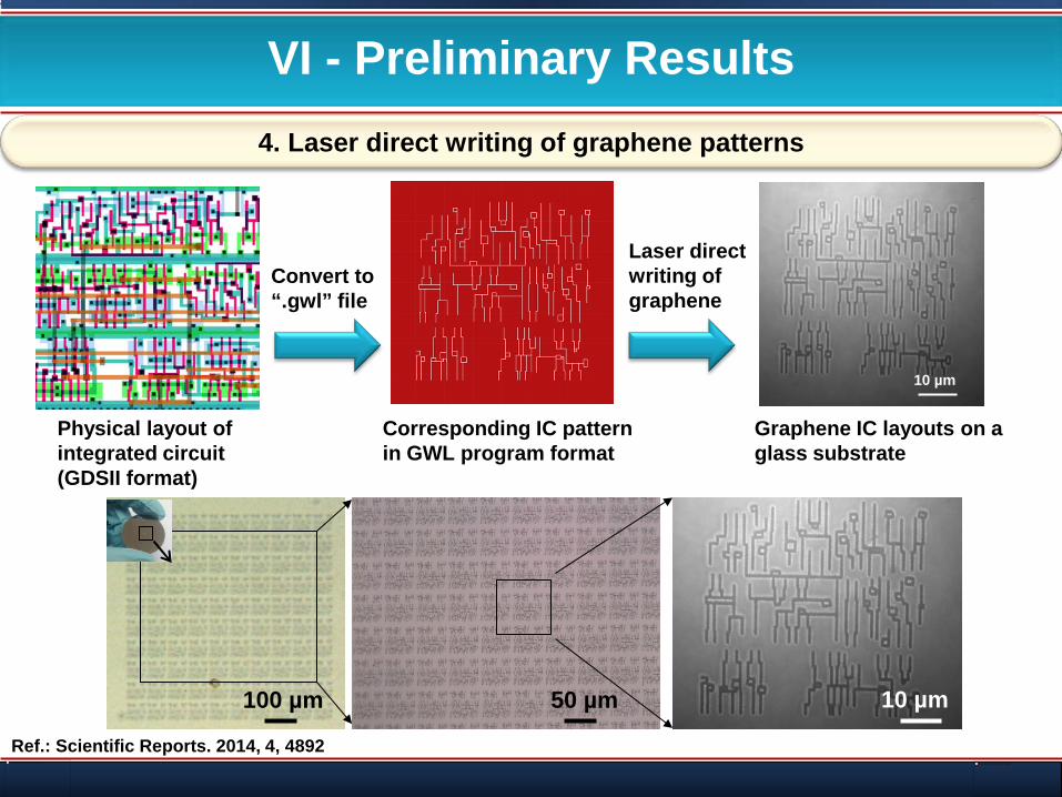
VI - Preliminary Results
Ref.: Scientific Reports. 2014, 4, 4892
Physical layout of integrated circuit (GDSII format)
Convert to “.gwl” file
Corresponding IC pattern in GWL program format
Graphene IC layouts on a glass substrate
Laser direct writing of graphene
10 µm
50 µm 10 µm 100 µm
4. Laser direct writing of graphene patterns

This image cannot currently be displayed.This image cannot currently be displayed.
VI - Preliminary Results
5. Resonant vibrational excitation in diamond growth control
(10.532 μm)
(10.532 μm)
(10.532 μm)

This image cannot currently be displayed.This image cannot currently be displayed.
VI - Preliminary Results
5. Resonant vibrational excitation in diamond growth control

This image cannot currently be displayed.This image cannot currently be displayed.
VI - Preliminary Results
5. Resonant vibrational excitation in diamond growth control
e) λ=10.551 µm
10 µm
b) λ=10.494 µm
10 µm
c) λ=10.513 µm
10 µm
f) λ=10.571 µm
10 µm
d) λ=10.532 µm
10 µm
a) No laser
10 µm

This image cannot currently be displayed.This image cannot currently be displayed.
VI - Preliminary Results
5. Resonant vibrational excitation in diamond growth control
10.48 10.50 10.52 10.54 10.56 10.580
20
40
60
80
Abso
rptio
n pe
rcen
tage
(%)
Wavelength (µm)
Flame Ethylene gas
10.476 10.494 10.513 10.532 10.551 10.571 10.591
2900
3000
3100
3200
CH ro
tatio
nal t
empe
ratu
re (K
)
Laser Wavelength (µm)
No laser
Flame temperature
10.494 10.513 10.532 10.551 10.5715
10
15
20
25
30
35
40
45
Depo
stio
n Ra
te (µ
m/h
r)
Laser Wavelength (µm)
Deposition rate without laser excitations
40.8 µm
7.2 µm, No laser
10.494 10.513 10.532 10.551 10.571
99.5
99.6
99.7
99.8
99.9
Q i (%
)
Wavelength (µm)
Qi without laser excitation
99.87%
99.49%, No laser
Diamond quality Deposition rate
Flame absorption rate

This image cannot currently be displayed.This image cannot currently be displayed.
VI - Preliminary Results
6. Low-temperature synthesis of GaN thin films
This image cannot currently be displayed.This image cannot currently be displayed.
Thank you!