v1s1_3
TRANSCRIPT
7/28/2019 v1s1_3
http://slidepdf.com/reader/full/v1s13 1/6
International Journal of Scientific Engineering and Technology(ISSN:Applied)
Volume No.1,Issue No.1 pg:16-22 Dec.2011
SAW Filter Performance Improvement Monali R. Dave
Department of Electronics & CommunicationSagar Institute of Research and Technology,Bhopal M.P. India
Mo nalij o shi2009 @g mail. co m
Abstract: Surface acoustic wave (SAW) filters have a wide
range of applications, including, for example, in
mobile/wireless transceivers, radio frequency (RF) filters,
intermediate frequency (IF) filters, resonator-filters, filters
for mobile and wireless circuits, IF filters in a base
transceiver station (BTS), RF front-end filters
for mobile/wireless circuitry, multimode frequency-
agile oscillators for spread-spectrum secure
communications, nyquist filters for microwave digital
radio, voltage controlled oscillators for first or second stagemixing in mobile transceivers, delay lines for low power
time-diversity wireless receivers, pseudo-noise-coded delay
lines for combined code division multiple access/time
division multiple access (CDMA/TDMA) access, clock
recovery filters for fiber-optics
communication repeater stages, synchronous, spread-
spectrum communications, televisions, video
recorders, and many other applications. SAW filters are
also finding increasing use as picture-signal intermediate-
frequency (PIF) filters, vestigial sideband (VSB) filters, and
other types of communication filters, and as filters for
digital signal processing [1]. It is, however, supported and lead
by various technologies of public
communication systems such as fiber optics, digital microwave
and satellites. Various custom SAW devices for publiccommunication systems have been already widely used and
still progress [2].
This paper describes various methods to minimize some of the
distortions in SAW filter. It includes bulk wave distortion and
feed through distortion.
I. Introduction
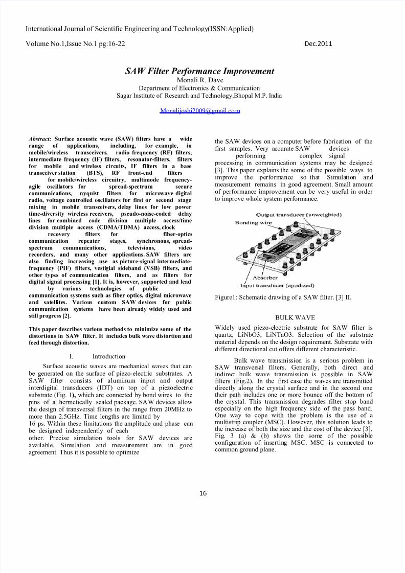
Surface acoustic waves are mechanical waves that can be generated on the surface of piezo-electric substrates. ASAW filter consists of aluminum input and outputinterdigital transducers (IDT) on top of a piezoelectricsubstrate (Fig. 1), which are connected by bond wires to the
pins of a hermetically sealed package. SAW devices allowthe design of transversal filters in the range from 20MHz tomore than 2.5GHz. Time lengths are limited by16 ps. Within these limitations the amplitude and phase can be designed independently of eachother. Precise simulation tools for SAW devices areavailable. Simulation and measurement are in goodagreement. Thus it is possible to optimize
the SAW devices on a computer before fabrication of thefirst samples. Very accurate SAW devices
performing complex signal processing in communication systems may be designed[3]. This paper explains the some of the possible ways toimprove the performance so that Simulation andmeasurement remains in good agreement. Small amountof performance improvement can be very useful in order
to improve whole system performance.
Figure1: Schematic drawing of a SAW filter. [3] II.
BULK WAVE
Widely used piezo-electric substrate for SAW filter isquartz, LiNbO3, LiNTaO3. Selection of the substratematerial depends on the design requirement. Substrate withdifferent directional cut offers different characteristic.
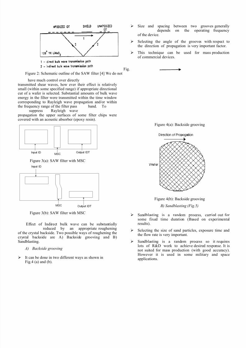
Bulk wave transmission is a serious problem inSAW transversal filters. Generally, both direct andindirect bulk wave transmission is possible in SAWfilters (Fig.2). In the first case the waves are transmitteddirectly along the crystal surface and in the second onetheir path includes one or more bounce off the bottom of
the crystal. This transmission degrades filter stop bandespecially on the high frequency side of the pass band.One way to cope with the problem is the use of amultistrip coupler (MSC). However, this solution leads tothe increase of both the size and the cost of the device [3].Fig. 3 (a) & (b) shows the some of the possibleconfiguration of inserting MSC. MSC is connected tocommon ground plane.
16
7/28/2019 v1s1_3
http://slidepdf.com/reader/full/v1s13 2/6
Figure 2: Schematic outline of the SAW filter [4] We do not
have much control over directlytransmitted shear waves, how ever their effect is relativelysmall (within some specified range) if appropriate directionalcut of a wafer is selected. Substantial amounts of bulk waveenergy in the filter were transmitted within the time windowcorresponding to Rayleigh wave propagation and/or withinthe frequency range of the filter pass band. To
suppress Rayleigh wave propagation the upper surfaces of some filter chips werecovered with an acoustic absorber (epoxy resin).
Figure 3(a): SAW filter with MSC
Figure 3(b): SAW filter with MSC
Effect of Indirect bulk wave can be substantiallyreduced by an appropriate roughening
of the crystal backside. Two possible ways of roughening thecrystal backside are A) Backside grooving and B)Sandblasting.
A) Backside grooving
It can be done in two different ways as shown inFig.4 (a) and (b).
Fig.
Size and spacing between two grooves generallydepends on the operating frequency
of the device.
Selecting the angle of the grooves with respect tothe direction of propagation is very important factor.
This technique can be used for mass productionof commercial devices.
Figure 4(a): Backside grooving
Figure 4(b): Backside grooving
B) Sandblasting (Fig.5)
Sandblasting is a random process, carried out for some fixed time duration (Based on experimentalresults).
Selecting the size of sand particles, exposure time andthe flow rate is very important.
Sandblasting is a random process so it requireslots of R&D work to achieve desired response. It isnot suited for mass production (with good accuracy).However it is used in some military and spaceapplications.

7/28/2019 v1s1_3
http://slidepdf.com/reader/full/v1s13 3/6
Selection of the roughening technique totallydepends on the system requirements and the results produced by particular technique.
Figure 5: Backside Sandblasting
For 128 YX LiNbO3 the effect of grooving onthe filter amplitude response can be evaluated bycomparison of Figs. 6 and 7. Application of groovingsubstantially improves stop band rejection of the filter.At some frequencies the improvement is greater than20 dB. The improvement is observed on both sidesof the pass band [4].
Figure 6: Measured amplitude responsesof the ungrooved filter
- - - - before covering the chip with epoxy resin after covering the chip with epoxy resin [4]
Figure 7: Measured amplitude responses of the grooved filter
- - - - - before covering the chip with epoxy resin after covering the chip with epoxy resin [4]
Improvement varies depending on the substratetype and its directional cut.
III. FEEDTHROUGH
After SAW device is placed in packages and secured by adhesive. Bond wires are attached between pads onthe device and the package, giving connections to theexternal terminals. The packages are sealed. The next stepis mounting this package on printed circuit board (PCB).To match the impedance of the device with the system,
external impedance matchingcomponents are needed, and these are usually added onPCB. At this stage, it is important to minimize feedthrough,which can degrade the stop-band rejection by generatingspikes in the stop-band. Feedthrough can be caused byinductive or capacitive coupling between the input and
output, or by a ground loop [5].
The SAW matched filters can be realized with thestructure called tapped delay line. It has one input andseveral output taps with different delay times. Figure 2illustrates a basic configuration of the conventional SAWmatched filter [6].

7/28/2019 v1s1_3
http://slidepdf.com/reader/full/v1s13 4/6
Figure 8: Conventional SAW matched filter consisting of multi-track tapped delay lines.
Figure 8 shows an impulse response of thefabricated device. We can hardly observe the mainresponse of SAW, as shown in Fig. 9(a). In Fig.9(b), the feed-through response is much larger than the desired time response. It is found that
the parasitic elements degrade the performance of the SAW matched filter in thehigh frequency range. In Fig. 10, the correlation
properties are awfully degraded by the spuriousresponse related to the feed-through. The D/Uratio is getting worse to 1.6 [6].
Figure 9 (a): Impulse responses of the conventional Figure 9 (b): Impulse responses of the conventional
SAW matched filter. (Frequency domain)[6] SAW matched filter. (Time domain) [6]
Figure 10: Correlation properties of the conventional SAW matched filter.

7/28/2019 v1s1_3
http://slidepdf.com/reader/full/v1s13 5/6
Proposed new configuration of SAW matchedfilters as illustrated in Fig. 11, in order to solve the feed-through problem. The new configuration has a single-endedinput and balanced outputs. The input-output1 and input-output2 patterns are designed to be symmetrical. Theindividual feed-through signals of output1
and output2 are in phase and the same magnitude, because of the symmetrical device pattern. On the contrary,the SAW IDT structures are designed as both desiredoutput signals are out of phase. Consequently, the feed-through signals can be canceled and only the desired signalcan be detected by using a balun [6].
Figure 11: Feed-through cancellation concept by symmetrical configuration. [6]
SAW Package
Cut / Slot in PCB
Matching Network Matching Network
PCB
Figure 12: Correlation properties of the new SAWmatched filter with symmetrical
configuration.To reduce the feedthrough effect some modifications
can also be done at PCB level. Inserting cuts/slots on PCB(Fig. 13) can help to improve the overall filter performance.
Figure 13: Modification in PCB III.
CONCLUSION
Paper presented the performanceimprovement in SAW filter stop band response by usingMSC, backside surface roughening, symmetric configurationand some modification in PCB. Typically 7 to 20 dBimprovement in stop band is achievable. This can be veryuseful in achieving desired specifications.

7/28/2019 v1s1_3
http://slidepdf.com/reader/full/v1s13 6/6
REFERENCES
[1] Electronics-manufacturersww w . e l e ct ro nic s -m a n u f a c tu r e r s .c o m / in fo / rf / m ic ro w av e - electronics/saw-filter.html
[2] Yasushi YAMAMOTO, “Saw filters and resonators for public communicationsystems”, NEC Corpomtion, Kawasaki, Kanamwa 211, and JAPAN.1051-0117/ 93/0000-0095 (c) 1993 IEEE, Page: 95
[3] Clemens C.W. Ruppel, IEEE Senior Member, and Leonhard Reindl, IEEE Member .Siemens Corporate Research and Development, “SAW Devices for Spread SpectrumApplications” Munich, Germany.0-7803-3567-8/96 (c) 1996 IEEE Page: 713, 714
[4] Piotr Naalows ki, Hanna Majewska “Parasitic bulk waves in wide band saw filtersdesigned on 128” rotated Y-CUT OF LiNbO3. Institute of Electronic MaterialsTechnology.W6lczyrSska 133, 01-91 9Warsaw, Poland European Frequency Time Forum, 5-7March 1996 Conference Publication No 418 @ IEE1996, Page: 159, 160, 161.
[5] COM DEV, “SAW Products” Note 104.
[6] Takahiro SATO (e-mail: tk -s at o @i eee . org), Tsuyoshi SUGIURA and Hiroyuki NAGASAKA. “Analysis of Parasitic Effects of GHz-range SAW Matched Filters for Wireless Pulse Communication Systems”. Samsung Yokohama Research Institute, Japan.0-7803-8412-
1/04/$20.00 (c) 2004 IEEE, Page: 1534, 1535, 1536.