v02 – verilog part 2 - computer sciencemarkov/ccsu_courses/v02-verilogpart02.pdf– 12 basic gates...
TRANSCRIPT

V02 – Verilog Part 2
Chapter 4. Section 4.12. pp. 164 - 182 Rev. 8/27/2013, 10/27/2013

Verilog II 2
HDL Models
• Modules are the basic building blocks for modeling• Three types of modules:
• Gate-level modeling• Uses pre-defined primates (and, not, or, other) or user-defined
primitives• Dataflow modeling
• Uses continuous assignment statements with keyword assign
• Behavioral modeling• Uses procedural assignment statements with keyword always
• Section 4.12 goes thru all three types

Verilog II 3
Gate-level Modeling
• Predefined primitives– 12 basic gates
and, nand, or, nor, xor, xnor, not, buf … others
• Most are n-input, 1-output • buf and not are single-input n-output primitives
– A single input can be connected to multiple lines– not( in, out1, out2, out2)

Verilog II 4
I. Gate-level Modeling

Verilog II 5
Logic Values
• 0 and 1 (for the usual false and true)
• x (for unknown)
• z (for high impedance)– IC pin not connected to anything,
• neither at ground ( value 0 ) nor at logic 1
– value of a 3-state gate that is not enabled
• Truth tables for circuits have to include x and z– AND gate: any input 0, output is 0– OR gate: any input 1, output is 1– Output of a logic gate other than 3-state is never z

Digital Design: With an Introduction to the Verilog HDL, 5eM. Morris Mano • Michael D. Ciletti
Copyright ©2013 by Pearson Education, Inc.All rights reserved.
Table 4.9 Truth Table for Predefined Primitive Gates

Verilog II 7
Vectors
Multi-bit widths are called vectors.
output [0:3] D;
wire [7:0] SUM
Output vector D, 4 bits wide, numbered 0 thru 3.
D[2] specifies bit 2 of D .
The first number (on the left) is the index of the most significant bit (MSB).
Bit numbering can go either way (MSB to LSB or LSB to MSB).
Wire SUM, 8 bits wide, numbered 0 thru 7. The MSB has index 7 .
SUM[2:0] specifies 3 least significant bits of SUM .
Verilog II 8
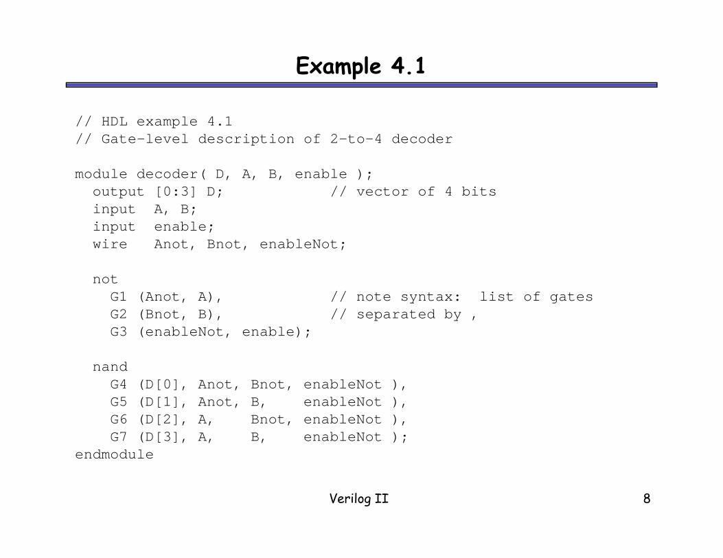
Example 4.1
// HDL example 4.1// Gate-level description of 2-to-4 decoder
module decoder( D, A, B, enable );output [0:3] D; // vector of 4 bitsinput A, B;input enable;wire Anot, Bnot, enableNot;
notG1 (Anot, A), // note syntax: list of gatesG2 (Bnot, B), // separated by ,G3 (enableNot, enable);
nandG4 (D[0], Anot, Bnot, enableNot ),G5 (D[1], Anot, B, enableNot ),G6 (D[2], A, Bnot, enableNot ),G7 (D[3], A, B, enableNot );
endmodule

Digital Design: With an Introduction to the Verilog HDL, 5eM. Morris Mano • Michael D. Ciletti
Copyright ©2013 by Pearson Education, Inc.All rights reserved.
FIGURE 4.19 Two-to-four-line decoder with enable-low input
0

Verilog II 10
Example 4.2 – Ripple-carry Adder
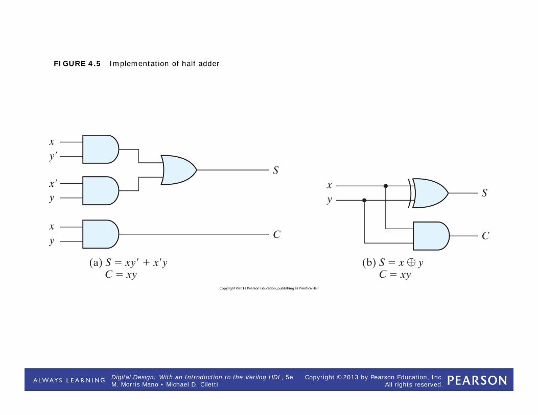
// Description of half adder (see Fig 4-5b) module halfadder (S, C, x, y);
input x, y; output S, C;
// Instantiate primitive gates xor (S, x, y); and (C, x, y);
endmodule
// Description of full adder (see Fig 4-8) module fulladder (S, C, x, y, z);
input x,y,z; output S,C; wire S1,D1,D2; //Outputs of first XOR and two AND gates
//Instantiate the halfadders halfadder HA1 (S1,D1,x, y),
HA2 (S, D2,S1,z); or g1(C,D2,D1);
endmodule

Verilog II 11
Example 4.2 – Ripple-carry Adder (continued)
// Description of 4-bit adder (see Fig 4-9) module Four_bit_adder (S,C4,A,B,C0);
input [3:0] A,B; input C0; output [3:0] S; output C4; wire C1,C2,C3; //Intermediate carries
// Instantiate the fulladder fulladder FA0 (S[0],C1,A[0],B[0],C0),
FA1 (S[1],C2,A[1],B[1],C1), FA2 (S[2],C3,A[2],B[2],C2), FA3 (S[3],C4,A[3],B[3],C3);
endmodule
Digital Design: With an Introduction to the Verilog HDL, 5eM. Morris Mano • Michael D. Ciletti
Copyright ©2013 by Pearson Education, Inc.All rights reserved.
FIGURE 4.5 Implementation of half adder

Digital Design: With an Introduction to the Verilog HDL, 5eM. Morris Mano • Michael D. Ciletti
Copyright ©2013 by Pearson Education, Inc.All rights reserved.
FIGURE 4.8 Implementation of full adder with two half adders and an OR gate

Digital Design: With an Introduction to the Verilog HDL, 5eM. Morris Mano • Michael D. Ciletti
Copyright ©2013 by Pearson Education, Inc.All rights reserved.
FIGURE 4.9 Four-bit adder

Verilog II 15
Test Bench for Adder
module testAdder;reg [3:0] A;reg [3:0] B;reg carryIn;wire [3:0] Sum;wire carryOut;
Four_bit_adder adder( Sum, carryOut, A, B, carryIn );
initialbeginA = 4'b1001; B = 4'b1011; carryIn = 1'b0;#10$display( " %b", A );$display( " %b", B );$display( "%b %b", carryOut, Sum );end
initial#20 $finish;
endmodule

Verilog II 16
Test
C:\iverilog\MyFiles iverilog –o adder mano4_2.vlC:\iverilog\MyFiles vvp adder
10011011
1 0100

Verilog II 17
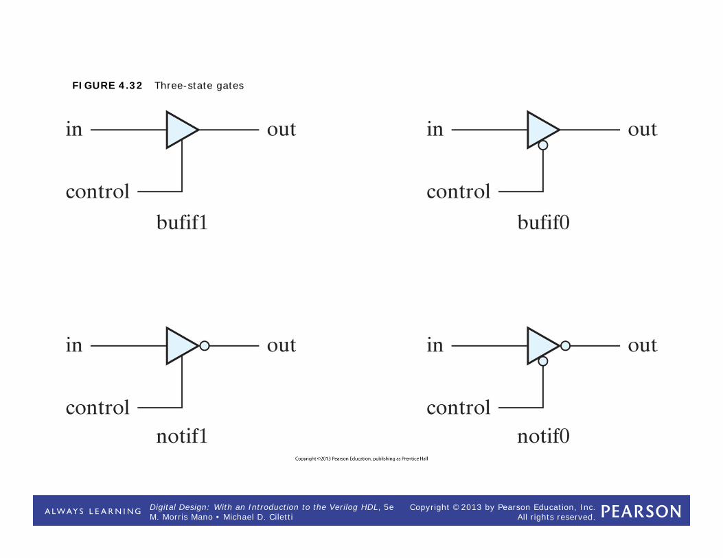
Three-state Gates
• Three-state gates have output values 0, 1, or z.• z is “high impedance”
• Verilog gates:• bufif1
• Output is z when control is 0• Output is same as input when control is 1
• bufif0• Output is z when control is 1• Output is same as input when control is 0
• notif1• Output is z when control is 0• Output is inverted input when control is 1
• notif0• Output is z when control is 1• Output is same as input when control is 0
Digital Design: With an Introduction to the Verilog HDL, 5eM. Morris Mano • Michael D. Ciletti
Copyright ©2013 by Pearson Education, Inc.All rights reserved.
FIGURE 4.32 Three-state gates

Verilog II 19
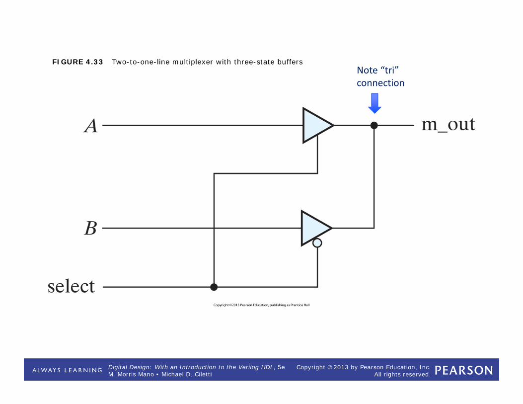
Mux implemented with 3-state Gates
module muxTri ( m_out, A, B, select )output m_out;input A, B, select;tri m_out; // can have several tri-state connections
bufif1(m_out, A, select );bufif0(m_out, B, select );
endmodule
Keyword tri is for a wire with several tri-state connections
tri is an example of a net data type, which represent connections betweenelements.
Other net types are wire, supply1, and supply0 (and others).
use supply1, and supply0 to hardwire an input to 1 or 0
Digital Design: With an Introduction to the Verilog HDL, 5eM. Morris Mano • Michael D. Ciletti
Copyright ©2013 by Pearson Education, Inc.All rights reserved.
FIGURE 4.33 Two-to-one-line multiplexer with three-state buffersNote “tri” connection

Verilog II 21
II. Dataflow modeling

Verilog II 22
Dataflow Modeling
Dataflow modeling uses operands that act on binary operands and produce binary results.
Be careful to distinguish binary addition + from AND operation &
assign gives a value to a net data type.
Net data types represent a physical connection between circuit elements, e.g. wire, or a port
assign Y = Boolean Expression using variables and operators.
continuous assignment : expression is always true as simulation runs(compare with procedural assignment : happens once, when thestatement gets control.)

Verilog II 23
Operators
Concatenation operator is { operand , operand }braces enclosing operands separated by comma
Equality test is == (two equal signs)
Bitwise AND is &operates on a vector of bits, does AND betweenbits in same position to produce a vector of bits
Logical AND is &&operates on a single true/false value to producea single true/false value. Non-0 is regarded astrue (as in programming language C).

Digital Design: With an Introduction to the Verilog HDL, 5eM. Morris Mano • Michael D. Ciletti
Copyright ©2013 by Pearson Education, Inc.All rights reserved.
Table 4.10 Some Verilog HDL Operators

Verilog II 25
// HDL example 4.3// -- textbook’s code has some typo’s and unneeded ()
module decoder( D, A, B, enable );output [0:3] D;input A, B;input enable;
assignD[0] = ! ( !A && !B && !enable ),D[1] = ! ( !A && B && !enable ),D[2] = ! ( A && !B && !enable ),D[3] = ! ( A && B && !enable );
endmodule
Dataflow description of 2-to-4 enable-low decoder
Compare with gate-level modeling, example 4.1 slide 8

Verilog II 26
// Data Flow Description of 4-bit adder (Ex. 4.4 )//module Four_bit_adder (S, C4, A, B, C0);
input [3:0] A, B; input C0; output [3:0] S; output C4;
assign {C4, S} = A + B + C0 ; endmodule
Dataflow description 4-bit Adder
Compare with gate-level modeling, example 4.2, p. 10See Figure 4.9.
Note concatenation operator in assign statement.
Same test bench can be used as with previous adder model.

Verilog II 27
// Dataflow description of a 2-to-1 mux//module mux ( m_out, A, B, select);
output m_out;input A, B, select;
assign m_out = select ? A: B ;endmodule
Conditional Operator
Condition ? trueExpression : falseExpression
The Condition is evaluated. If true, the value of the entire expression is trueExpression.If false, the value of the entire expression is falseExpression.
Verilog II 28
III. Behavioral Modeling

Verilog II 29
Behavioral Modeling
• Represents digital circuits at an algorithmic level.
• keyword initial indicates a process that starts running when the simulation starts, but runs just once.
• keyword always indicates a process that starts waiting for a trigger when the simulation starts.
• keyword always is followed by an event control expression, and then a list of procedural assignment statements.
procedural assignment statement like assignment statement in C or Java.
Target of a procedural assignment statement must be of regtype.
reg (register) holds its value until changed.
This is a loop, but each iteration is triggered by the event control. (Somewhat like event-driven programming.)

Verilog II 30
always
always @(a or b) // Any time a or b CHANGE, run the blockbegin if (a) c = b;
else d = ~b;
end // End of block
There might be several initial and several always blocks in a simulation.
They all start together at time 0 in the simulation.
All of the initial blocks start up and run to the end of the block and then stop (although there may be time delays inside) .
All of the always blocks start up looking at their control expression and are triggered whenever it is true, then run to the end of the block, then start waiting to be triggered again.

Verilog II 31
loop
always begin // Always begins executing at time 0 and NEVER stops clk = 0; // Set clk to 0 #1; // Wait for 1 time unit clk = 1; // Set clk to 1 #1; // Wait 1 time unit end
// Keeps executing - so continue back at the top of the begin
Always used without the event control expression

Verilog II 32
Mux Example
// Behavioral description of 2-to-1-line multiplexer// HDL Example 4.7 module mux2x1(OUT, A, B, select);
input A,B,select; output OUT; reg OUT; // OUT must be reg type since it is assigned toalways @ (A or B or select)
if (select == 1) OUT = A; else OUT = B;
endmodule
Also could have: always @ ( select, A, B )
(Note typo in book: p. 175, line 8 of program, change 5 to = )

Verilog II 33
case Example
//Behavioral description of 4-to-1-line multiplexer //Describes the function table of Fig. 4-25(b). module mux4x1_bh (i0, i1, i2, i3, select, y);
input i0,i1,i2,i3; input [1:0] select; output y; reg y; always @ (i0 or i1 or i2 or i3 or select)
case (select) 2'b00: y = i0; 2'b01: y = i1; 2'b10: y = i2; 2'b11: y = i3;
endcaseendmodule
Works much like Java case statement.

FIGURE 4.25 Four-to-one-line multiplexer

Verilog II 35
Test Benches

Verilog II 36
Test Bench
• A test bench is an HDL program that describes signals to be sent to a circuit.– Tests if the circuit behaves as intended.
• Sometimes called a “stimulus.”• Signals should include all combinations of values.• Ideally:
– the circuit model has only gates, dataflow statements, or behavioral statements.
– The test bench contains the output statements, like $display or $monitor.
– Analogy to actual electronics lab:• The circuit is a breadboard containing the electronic components.• The circuit is tested with signal generators, probes, and scopes.

Verilog II 37
Time Delays
• Test benches usually have several processes running in parallel,• specified with always and initial keywords, • usually have time delays inside of them.• #10 means to delay for 10 ticks of simulated time.
– For us, just measure time in “ticks.”
initialbegin
A = 0; B = 0;#10 A = 1;#20 A = 0; B = 1;
end
Verilog II 38
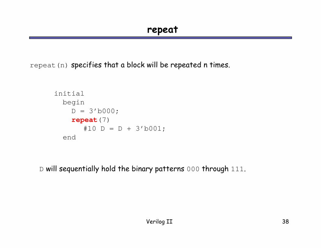
repeat
repeat(n) specifies that a block will be repeated n times.
initial beginD = 3’b000;repeat(7)
#10 D = D + 3’b001;end
D will sequentially hold the binary patterns 000 through 111.

Verilog II 39
Usual Form
module testBenchName;// declare local reg and wire identifiers// instantiate the circuit module, binding local// identifiers to module’s identifiers// generate a sequence of stimulus values// using always and initial// display the output of the module
endmodule
Test modules usually have no inputs nor outputs, but create inputs for the circuit under test and display that circuit’s outputs.
When the circuit model is instantiated, the identifiers in the test bench are bound to the formal identifiers in the circuit model.
-- like variables of main bound to parameters of a function.

Digital Design: With an Introduction to the Verilog HDL, 5eM. Morris Mano • Michael D. Ciletti
Copyright ©2013 by Pearson Education, Inc.All rights reserved.
FIGURE 4.34 Interaction between stimulus and design modules
Outputs of the circuit should be matched to wires in the test bench.

Verilog II 41
System Tasks
• Systems tasks are built-in functions.• Start with $.
$display -- display the current value of the variables in a list$write -- same as $display, but does not go to next line$monitor -- display the current value of the variables in a list
each time one of them changes.$time -- current simulation time (for us, in ticks)$finish -- terminate the simulation
Look in book for further details.