using microcontrollers in digital signal processing ... · pdf fileusing microcontrollers in...
TRANSCRIPT
Rev. 0.2 8/08 Copyright © 2008 by Silicon Laboratories AN219
AN219
Using Microcontrollers in Digital Signal Processing Applications
1. IntroductionDigital signal processing algorithms are powerful tools that provide algorithmic solutions to common problems. Forexample, digital filters provide several benefits over their analog counterparts. These algorithms are traditionallyimplemented using dedicated digital signal processing (DSP) chips, FPGAs, or RISC processors. While thesesolutions are very efficient at their purpose, they only perform one function in the system and can be bothexpensive and large. This application note discusses an alternative solution using a Silicon Labs microcontroller toimplement DSP algorithms in less space and still have plenty of CPU bandwidth available for other tasks.
This application note discusses the implementation of three DSP solutions on the C8051F12x and C8051F36xfamily of microcontrollers:
FIR filters
Goertzel Algorithm used for DTMF decoding
FFT algorithm
For each of these topics, we introduce the algorithm, discuss the implementation of these algorithms on the DSP-enabled MCUs using the multiply and accumulate (MAC) engine, and provide a list of the CPU bandwidth andmemory usage.
1.1. Key PointsThe 100 peak MIPS CPU, 2-cycle 16x16 MAC engine and on-chip ADC and DAC make the C8051F12x andC8051F36x well suited to DSP applications. Using these resources on a C8051F36x microcontroller, a 5x5 mm 8-bit MCU can process data in real-time for FIR filters and Goertzel Algorithms for DTMF decoding and implementa full FFT.
2. Digital FIR FiltersFilters have many applications, including narrowing the input waveform to a band of interest and notching outundesired noise. Digital filters have some benefits over their analog counterparts. For example, they are extremelyreconfigurable since they only rely on digital numbers, which are easily changeable, to determine the filterbehavior. The response of analog filters is determined by external components, which must be replaced if thefilter’s behavior is to be altered. Additionally, digital filters typically require fewer external components, whichreduces manufacturing cost and improves reliability. External components, such as resistors and capacitors, canalso be sensitive to temperature change and aging effects, which can alter the filter’s behavior if the environmentchanges. Since a digital filter is algorithmic, its behavior is not affected when the environment changes.
There are two types of digital filters: infinite impulse response (IIR) and finite impulse response (FIR). IIR filtershave a non-zero response over time to an input impulse. The output of an IIR filter relies on both previous inputsand the previous outputs. FIR filters settle to zero over time. The output of an FIR filter relies on previous inputsonly and does not rely on previous outputs.
2.1. Digital Filter AlgorithmsThe digital filter equations are based on the following basic transfer function shown in the z domain:
Y(z) = H(z)X(z),
where Y(z) is the filter output, X(z) is the filter input, and H(z) is the transfer function of the filter.
H(z) can be expanded as follows:
where a and b are sets of coefficients and z is a delay element.
Y z b 1 b 2 z 1– b+ + + n 1+ z n–
a 1 a 2 z 1– a+ + + n 1+ z n–---------------------------------------------------------------------------------------X z =
AN219
2 Rev. 0.2
2.1.1. IIR Filter Algorithm
The IIR topology extends directly from this equation by moving the denominator of the expanded H(z) to the leftside of the equation:
(a(1)+a(2)z–1+…+a(n+1)z–n)Y(z) = (b(1)+b(2)z–1+…+b(n+1)z–n)X(z)
In the time domain, this equation appears as follows:
a(1)y(k) + a(2)y(k –1)+…+a(n+1)y(k –n) = b(1)x(k) + b(2)x(k –1)+…+b(n+1)x(k –n)
where y(k) represents the current filter output, x(k) represents the current input, y(k-1) represents the previousoutput, x(k-1) represents the previous input, and so on. If this equation is solved for y(k):
This equation shows that the IIR filter is a feedback system, which generates the current output based on thecurrent and previous inputs as well as the previous outputs. The IIR structure has unique advantages anddrawbacks. The main advantage of the IIR structure is that it provides a frequency response comparable to an FIRfilter of a higher order. This results in fewer calculations necessary to implement the filter. IIR filters can suffer frominstability because they rely on feedback. As a result, they are more difficult to design and special care must betaken to prevent an unstable system. IIR filters may also have a non-linear phase response, which can make theminappropriate for some applications where linear phase is necessary. Finally, because they rely on past outputs,they tend to be more sensitive to quantization noise, making them difficult to implement with 16-bit fixed pointhardware. Generally, 32-bit hardware is necessary for an IIR filter implementation.
2.1.2. FIR Filter Algorithm
In contrast, an FIR filter has no feedback. The filter transfer function can be derived in the same way as before.However, there is only one a coefficient and it is equal to one (a(1) = 1). When solving the equation for y(k):
For the FIR algorithm, the current output is generated based only on the current and previous inputs. In effect, anFIR is a weighted sum operation.
FIR filters have several advantages and drawbacks. One of the main advantages is that FIR filters are inherentlystable. This characteristic makes designing FIR filters easier than designing IIR filters. In addition, FIR filters canprovide linear phase response which may be important for some applications. Another important advantage of FIRfilters is that they are more resistant to quantization noise in their coefficients. As a result, they can be readilyimplemented using 16-bit fixed point hardware such as the Multiply and Accumulate module on the C8051F12xand C8051F36x. The main drawback of FIR filters is that they require significantly more mathematical operations toachieve a response similar to an IIR filter. Because of the ease of design and their compatibility with fixed-pointmicrocontrollers, the FIR filter will be the focus of the implementation discussion for the rest of this application note.
Replacing a(1)=1 and C for the b constants, the equation for the FIR filter is as follows:
y(n) = C0x(n) + C1x(n-1) + C2x(n-2) + C3x(n-3) + …,
where y(n) is the most recent filter output and x(n) is the most recent filter input. The filter does rely on previousinputs, as shown by the x(n-1), x(n-2), etc. terms. The Cx constants determine the filter response and can bederived using many different algorithms, each yielding different characteristics.
y k b 1 x k b+ 2 x k 1– b+ + n 1+ x k n– a 2 y k 1– – a– n 1+ y k n– –
a 1 -------------------------------------------------------------------------------------------------------------------------------------------------------------------------------------------------------------------------------=
y k b 1 x k b 2 x k 1– b n 1+ x k n– + + +a 1
---------------------------------------------------------------------------------------------------------------------------=

AN219
Rev. 0.2 3
This algorithm works as follows:
The first input, x(1) is multiplied by C0. The output y(1) is as follows:
y(1) = C0x(1)
The x(1) input is then saved for the next pass through the FIR algorithm.
The second input, x(2) is multiplied by C0 and the previous input x(1) is multiplied by C1. The output y(2) is asfollows:
y(2) = C0x(2) + C1x(1)
The x(1) and x(2) inputs are saved for the next input x(3), and so on.
The order of an FIR filter is equal to one less than the number of constants and is an indication of the degree ofcomplexity and the number of input samples that need to be stored. The higher the order, the better thecharacteristics of the filter (sharper curve and flatter response in the non-attenuation region).
2.2. FIR Algorithm Implementation on the C8051F12x and C8051F36xThe C8051F12x and C8051F36x MAC engine is uniquely suited to implement FIR algorithms. Each pass throughthe filter requires multiplies and accumulates, which the MAC engine was designed to implement quickly andefficiently. Coupled with the 100 MIPS 8051 processor, the ‘F12x and ‘F36x are able to calculate the FIR filteralgorithm in real time while still leaving ample CPU resources available for other tasks.
2.2.1. Implementation Optimizations
In the FIR algorithm, the previous inputs to the filter are used in each output calculation. Instead of shuffling thesedata points through an array to place the newest input in the same place (address 0, for instance), the FIRalgorithm can use a circular buffer structure to handle the flow of input samples. The circular buffer uses an arrayand saved indexes to overwrite the oldest sample with the newest sample and to process the inputs in their properorder. This structure provides a way to correctly match input samples with their corresponding filter coefficientswithout excessive data movement overhead.
FIR Filters have an interesting coefficient mirroring property that allows for significant optimization of the filteralgorithm. After generating the coefficients for a particular filter, the coefficients will always be mirrored around thecenter coefficient. For an example, in an n order filter, the first coefficient C0 is equal to the last coefficient Cn, thecoefficient C1 is equal to the coefficient Cn-1, etc. A benefit of this property is that half of the instructions used toload the coefficients into the MAC can be avoided. Instead, each coefficient can be loaded into the MAC andfollowed sequentially by the two samples that will be multiplied with it. This reduces the data movement operationsto the MAC by approximately 25% and offers substantially better filter performance.
Furthermore, some filters have a second property where every other coefficient has a value of zero that allows foreven more optimization. This occurs in Half-Band filters which have a frequency response that is symmetric about1/2 of the Nyquist rate (1/4th of the Sampling Rate). These multiplications with the zero value coefficients do notneed to be performed, as the result will just be zero and the accumulated output will not change. Removing theseunnecessary multiplications from the filter loop has a substantial impact on execution time.
2.2.2. FIR Filter Example
An application uses an FIR filter to perform a task. For example, a voice application may use a low-pass FIR filter toattenuate frequencies above 4 kHz. To demonstrate the FIR algorithm on the DSP-enabled MCUs, theFIR_Demo.c programs measure the frequency response of the filter between 50 Hz and 5 kHz. The programsrecord the input RMS value and the output RMS value of the filter at the current frequency and print the frequency,input RMS value, and output RMS value to the UART. They then increase the generated frequency and beginagain. The programs utilize the IDAC to generate the frequency sweep and use an ADC sampling frequency of10 kHz. The RMS value for the input and output are calculated and used in the output power calculation.
AN219
4 Rev. 0.2
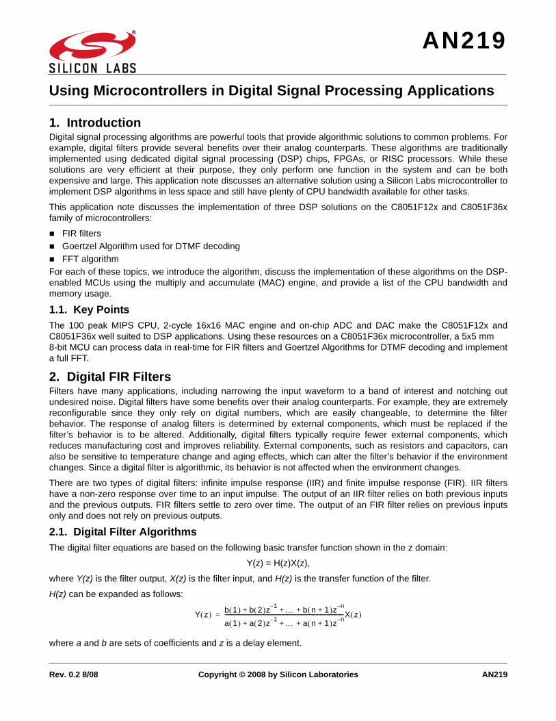
This application note FIR example code takes advantage of the circular buffer and mirroring optimizations, sincethese are properties of all FIR filters. The Half-Band property is only applicable to some FIR designs, so thisoptimization is not included. Figure 1 illustrates the FIR firmware procedure.
Figure 1. FIR Filter Firmware Flow Diagram
Initialize the system (Oscillator, Port I/O, ADC, DAC, UART, Timers, and MAC).
Output DAC frequency.
Sample DAC frequency with ADC.
Yes
No
Load sample into FIR circular buffer.
Load one coefficient into the MAC and multiply by the two corresponding ADC samples.
If necessary, calculate middle coefficient for odd number of TAPS.
Sample DAC frequency with ADC.
Calculate RMS value of the FIR filter.
Calculate RMS value of the input waveform.
Output current frequency, output RMS value, and input RMS value through the UART.
Increment the DAC frequency by 10 Hz.
No
Start
End
Yes
Yes
No
Store the filtered sample in an array.
Number of inputs equal to N?
Number of iterations equal to TAPS/2?
Frequency equal to 5 kHz?
AN219
Rev. 0.2 5
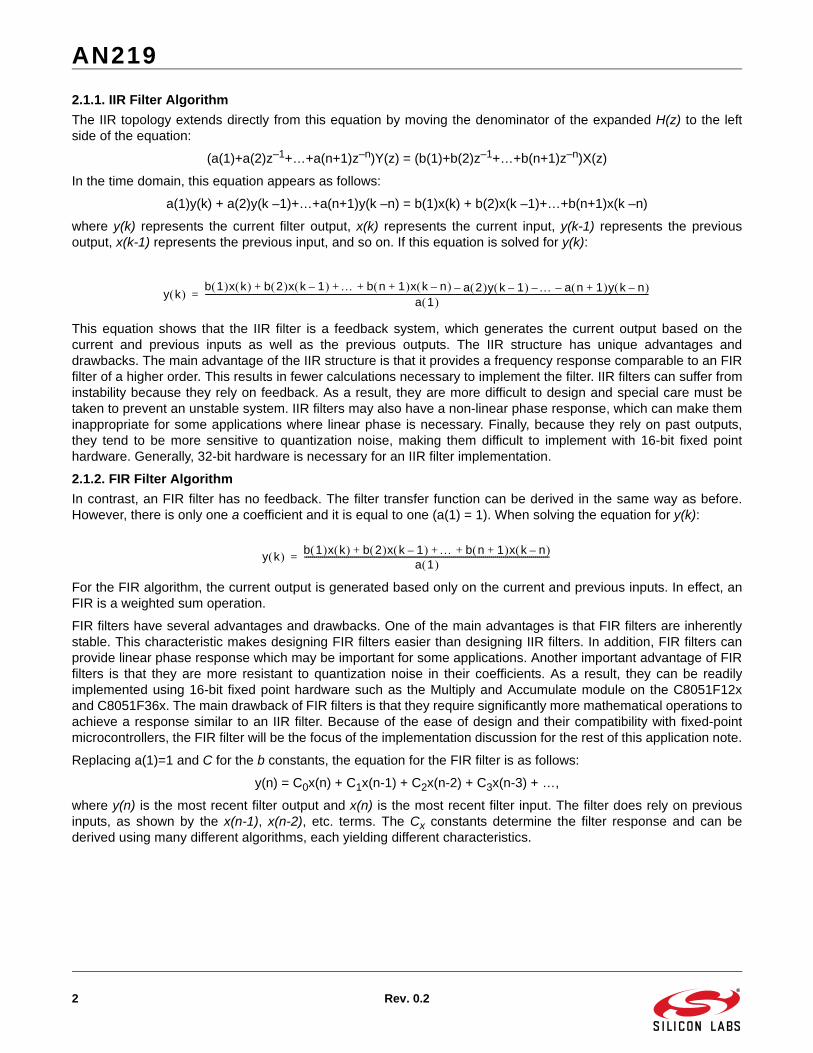
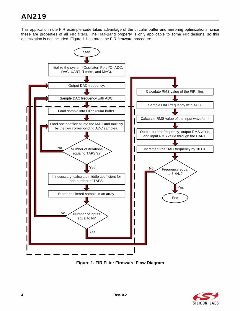
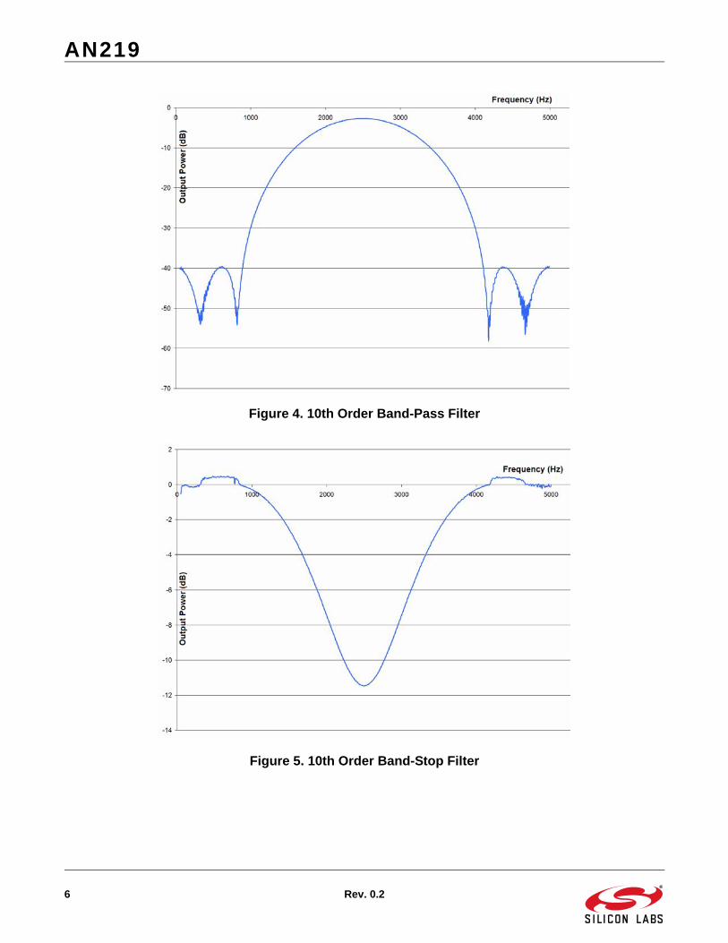
Figures 2 through 5 illustrate the frequency responses of several different filters designed using FDATool(MATLAB) and implemented on the C8051F12x and C8051F36x family of devices. In all cases, the filter responseoutput from the microcontroller matches the filter response designed in FDATool.
Figure 2. 10th Order Low-Pass Filter
Figure 3. 10th Order High-Pass Filter
AN219
6 Rev. 0.2
Figure 4. 10th Order Band-Pass Filter
Figure 5. 10th Order Band-Stop Filter
AN219
Rev. 0.2 7
2.3. Running the FIR DemoCompiling the FIR Demo example code will require either the full version of the Keil compiler (because of the codesize and the sqrt() function) or SDCC. This firmware is located in the associated application note software packageavailable on the Silicon Labs MCU Applications webpage.
For the hardware setup specific to the C8051F120 Target Board or C8051F360 ToolStick daughter card, refer to "5.Hardware Setup" on page 22.
To recompile the program, open the Silicon Laboratories IDE and add the appropriate FIR_Demo.c file to theproject and build. Under the ProjectTool Chain Integration menu, select the compiler and executable paths. Theexample code is intended for either the C8051F120 Target Board or the C8051F360 ToolStick daughter card,though the programs can be modified for alternate platforms. Build the project, connect to the target device, anddownload the code.
Connect to the C8051F120 using the RS-232 connector on the Target Board and a terminal program (likeHyperTerminal). Connect to the ‘F360 ToolStick daughter card board using the ToolStick Terminal program. Savethe output to a file and use the FIR_graph.xls Excel spreadsheet to graph the filter response (instructions can befound in the spreadsheet).
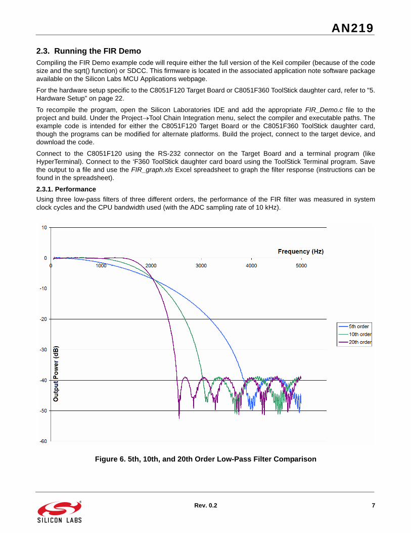
2.3.1. Performance
Using three low-pass filters of three different orders, the performance of the FIR filter was measured in systemclock cycles and the CPU bandwidth used (with the ADC sampling rate of 10 kHz).
Figure 6. 5th, 10th, and 20th Order Low-Pass Filter Comparison
AN219
8 Rev. 0.2
The performance of the C8051F12x and C8051F36x families of microcontrollers are as follows with the threedifferent filter orders:
Even with a 20th order filter, the filter only takes 9.3% of the microcontroller bandwidth, allowing the MCU tocomplete many other tasks or, if no other tasks are required, sleep and conserve power when not in use.
Code Segment 25 MIPS MAC implementation 98 MIPS MAC implementation
Clock cycles
us MCU bandwidth Clock cycles
us MCU bandwidth
5th order FIR filter 289 11.6 11.6% 289 2.9 2.9%
10th order FIR filter 513 20.5 20.5% 513 5.2 5.2%
20th order FIR filter 913 36.5 36.5% 913 9.3 9.3%
AN219
Rev. 0.2 9
3. Goertzel Algorithm
Many embedded systems are interested in a single or small set of frequencies in an input waveform. The GoertzelAlgorithm is a useful tool when these frequencies of interest are known.
The Goertzel Algorithm is a specialized algorithm intended to detect the presence of a single frequency. It isimplemented in the form of a two-pole IIR filter, though the derivation comes from a single-bin Discrete FourierTransform output*.
*Note: Lyons, Richard. Understanding Digital Signal Processing. Second Edition. 2004.
The Goertzel equations are as follows:
Q0 = (coefk × Q1[n]) - Q2[n] + x[n],
Q1 = Q0[n – 1],
Q2 = Q1[n – 1],
where x[n] is the current input, Q0 is the latest output, Q1 is the output from the previous iteration, and Q2 is theoutput from two iterations ago. The coefficient coefk is dependant upon certain system parameters like the targetfrequency and the total number of inputs N. The power of the input waveform at a particular frequency is as follows:
Power = magnitude2 = Q12[N] + Q22[N] - (coefk × Q1[N] × Q2[N])
Because of the Discrete Fourier Transform influence in the Goertzel equations, the algorithm does not have a validoutput until n, the current input number, is equal to N, which is the total number of inputs used by the algorithm.This means that the output of the filter is not valid until it has processed N input samples.
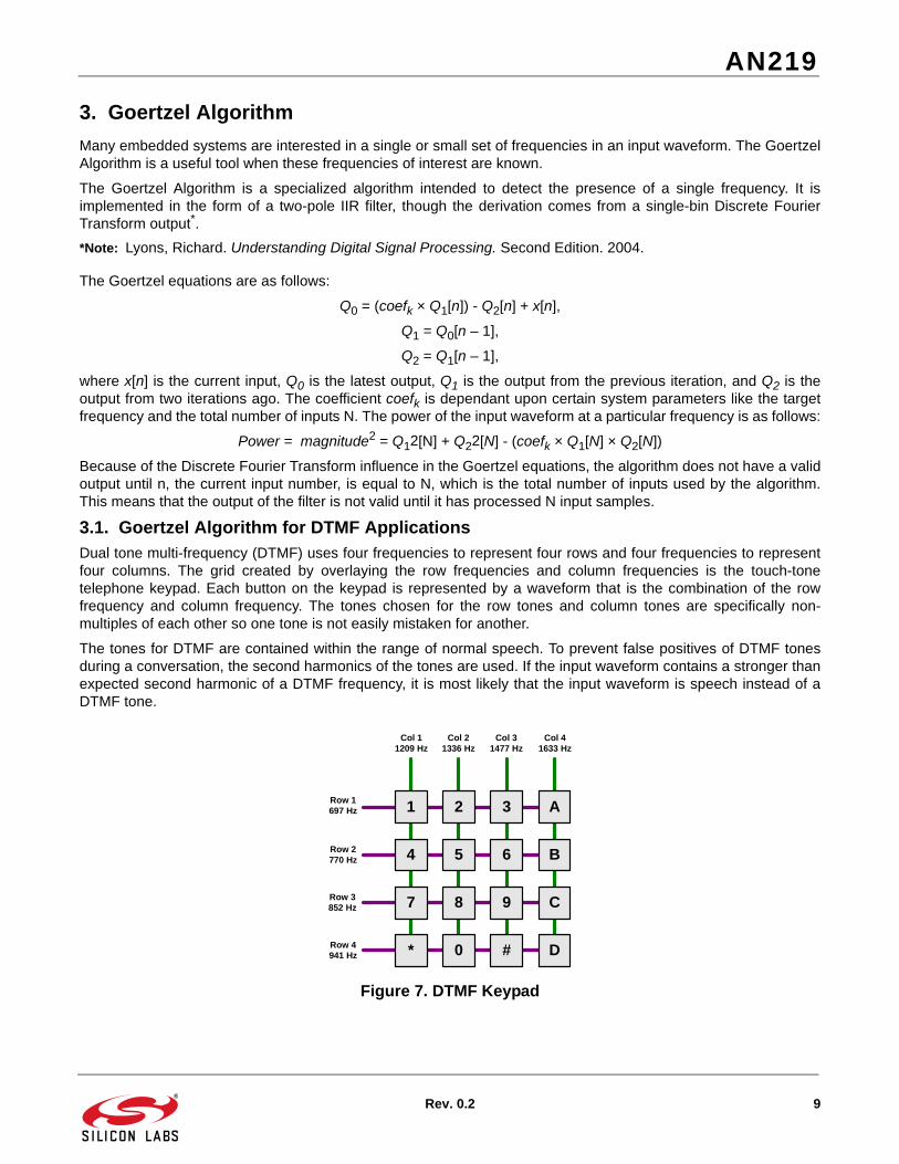
3.1. Goertzel Algorithm for DTMF ApplicationsDual tone multi-frequency (DTMF) uses four frequencies to represent four rows and four frequencies to representfour columns. The grid created by overlaying the row frequencies and column frequencies is the touch-tonetelephone keypad. Each button on the keypad is represented by a waveform that is the combination of the rowfrequency and column frequency. The tones chosen for the row tones and column tones are specifically non-multiples of each other so one tone is not easily mistaken for another.
The tones for DTMF are contained within the range of normal speech. To prevent false positives of DTMF tonesduring a conversation, the second harmonics of the tones are used. If the input waveform contains a stronger thanexpected second harmonic of a DTMF frequency, it is most likely that the input waveform is speech instead of aDTMF tone.
Figure 7. DTMF Keypad
D
Row 1697 Hz
Row 2770 Hz
Row 3852 Hz
Row 4941 Hz
Col 11209 Hz
Col 21336 Hz
Col 31477 Hz
Col 41633 Hz
#0*
7 8 9 C
B654
1 2 3 A
AN219
10 Rev. 0.2
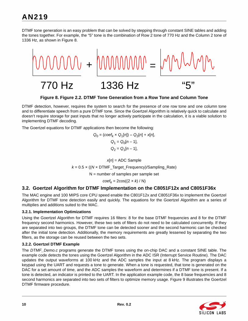
DTMF tone generation is an easy problem that can be solved by stepping through constant SINE tables and addingthe tones together. For example, the “5” tone is the combination of Row 2 tone of 770 Hz and the Column 2 tone of1336 Hz, as shown in Figure 8.
Figure 8. Figure 2.2. DTMF Tone Generation from a Row Tone and Column Tone
DTMF detection, however, requires the system to search for the presence of one row tone and one column toneand to differentiate speech from a pure DTMF tone. Since the Goertzel Algorithm is relatively quick to calculate anddoesn’t require storage for past inputs that no longer actively participate in the calculation, it is a viable solution toimplementing DTMF decoding.
The Goertzel equations for DTMF applications then become the following:
Q0 = (coefk × Q1[n]) – Q2[n] + x[n],
Q1 = Q0[n – 1],
Q2 = Q1[n – 1],
x[n] = ADC Sample
k = 0.5 × ((N × DTMF_Target_Frequency)/Sampling_Rate)
N = number of samples per sample set
coefk = 2cos((2 × k) / N)
3.2. Goertzel Algorithm for DTMF Implementation on the C8051F12x and C8051F36xThe MAC engine and 100 MIPS core CPU speed enable the C801F12x and C8051F36x to implement the GoertzelAlgorithm for DTMF tone detection easily and quickly. The equations for the Goertzel Algorithm are a series ofmultiplies and additions suited to the MAC.
3.2.1. Implementation Optimizations
Using the Goertzel Algorithm for DTMF requires 16 filters: 8 for the base DTMF frequencies and 8 for the DTMFfrequency second harmonics. However, these two sets of filters do not need to be calculated concurrently. If theyare separated into two groups, the DTMF tone can be detected sooner and the second harmonic can be checkedafter the initial tone detection. Additionally, the memory requirements are greatly lessened by separating the twofilters, as the storage can be reused between the two sets.
3.2.2. Goertzel DTMF Example
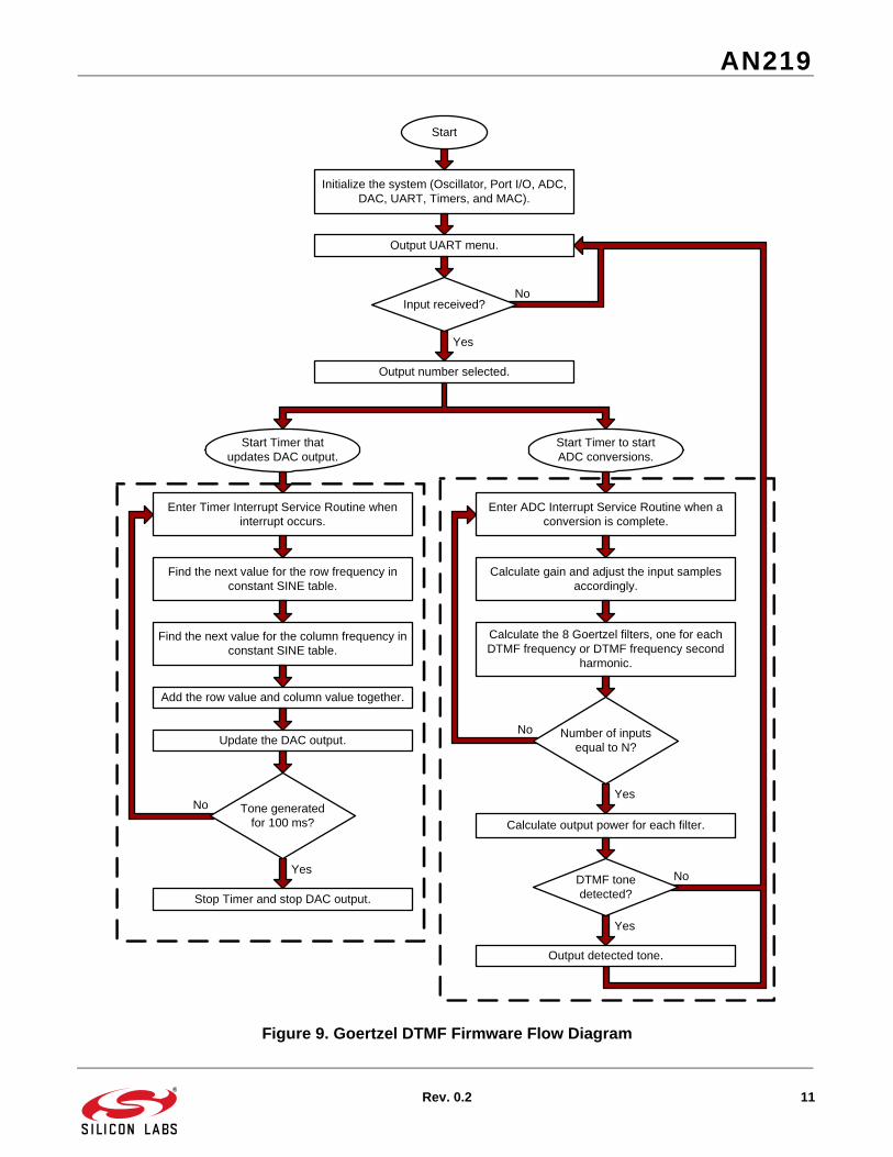
The DTMF_Demo.c programs generate the DTMF tones using the on-chip DAC and a constant SINE table. Theexample code detects the tones using the Goertzel Algorithm in the ADC ISR (Interrupt Service Routine). The DACupdates the output waveforms at 100 kHz and the ADC samples the input at 8 kHz. The program displays akeypad using the UART and requests a tone to generate. When a tone is requested, that tone is generated on theDAC for a set amount of time, and the ADC samples the waveform and determines if a DTMF tone is present. If atone is detected, an indicator is printed to the UART. In the application example code, the 8 base frequencies and 8second harmonics are separated into two sets of filters to optimize memory usage. Figure 9 illustrates the GoertzelDTMF firmware procedure.
+ =
770 Hz 1336 Hz “5”
AN219
Rev. 0.2 11
Figure 9. Goertzel DTMF Firmware Flow Diagram
Initialize the system (Oscillator, Port I/O, ADC, DAC, UART, Timers, and MAC).
Output UART menu.
Start
Output number selected.
Yes
NoInput received?
Start Timer that updates DAC output.
Start Timer to start ADC conversions.
Enter Timer Interrupt Service Routine when interrupt occurs.
Find the next value for the row frequency in constant SINE table.
Find the next value for the column frequency in constant SINE table.
Add the row value and column value together.
Update the DAC output.
Stop Timer and stop DAC output.
Yes
No
Enter ADC Interrupt Service Routine when a conversion is complete.
Calculate gain and adjust the input samples accordingly.
Calculate the 8 Goertzel filters, one for each DTMF frequency or DTMF frequency second
harmonic.
Yes
Calculate output power for each filter.
Output detected tone.
Yes
No
No
Tone generated for 100 ms?
Number of inputs equal to N?
DTMF tone detected?
AN219
12 Rev. 0.2
Because the example code generates the DTMF tone and detects it on the same device, there is a synchronizationbetween the systems that would not normally exist in an application. Separate generation and detection code isalso provided with this application note for systems where the two actions occur asynchronously on separateplatforms.
3.3. Running the Goertzel DTMF DemoThe Goertzel DTMF Demo requires either the full version of the Keil compiler (because the code size is larger than4 kB) or SDCC. This firmware is located in the associated application note software package available on theSilicon Labs Applications webpage.
For the hardware setup specific to the C8051F120 Target Board or C8051F360 ToolStick daughter card, refer to "5.Hardware Setup" on page 22.
To recompile the program, open the Silicon Laboratories IDE and add the DTMF_Demo.c file to the project andbuild. Under the ProjectTool Chain Integration menu, select the appropriate compiler and executable paths. Theproject is intended for either the C8051F120 Target Board or the C8051F360 ToolStick daughter card, though it canbe modified for alternate platforms. Build the project, connect to the target, and download the code.
Connect to the C8051F120 using the RS-232 connector on the Target Board and a terminal program (likeHyperTerminal). Connect to the ‘F360 ToolStick daughter card board using the ToolStick Terminal program.Navigate the UART menu to generate DTMF tones. The UART will output when a tone has been generated and ifa tone was detected before reprinting the menu.
3.4. PerformanceThe MAC engine and 100 MIPS core CPU speed allow the C8051F12x and C8051F36x family of microcontrollersto greatly outperform a 25 MIPS CPU running the same algorithm. This allows the ‘F12x and ‘F36x to calculate thealgorithms for eight filters concurrently and in real-time as the inputs are gathered. Furthermore, the ‘F12x and‘F36x can calculate the power for each frequency in real-time.
With the normal implementation running at 25 MIPS, the power calculations must occur in the background inbetween the calculations for each ADC input, and because so much of each sampling period is taken by thecalculations themselves, the power calculation results may be rather delayed. However, the ‘F12x and ‘F36ximplementation using the MAC and 100 MIPS CPU bandwidth are more than eight times faster and the filters andpower calculations can be completed entirely in the ADC ISR (Interrupt Service Routine) before the next ADCsample. Because of this, the power calculations and Goertzel filters don’t take nearly as much time away fromother tasks. In a 25 MIPS device, the DTMF application will take most of the bandwidth of the device, but the DSP-enabled microcontrollers can easily complete other tasks.
Furthermore, the normal implementation takes more code space (5355 bytes of code versus 5057 bytes of code)and more RAM (165 bytes versus 126 bytes) to implement than the MAC version of the algorithm.
Code Segment 25 MIPS non-MAC implementation
98 MIPS non-MAC implementation
98 MIPS MAC implementation
Clock cycles
us Clock cycles
us Clock cycles
us
8 Goertzel filters in ADC ISR
2095 83.8 2095 21.4 1018 10.4
Power calculations 13,113 524.5 13,113 133.8 1743 17.8
Total time for 200 input samples
432,000 17,285 432,000 4409 205,000 2095
AN219
Rev. 0.2 13
4. Fast Fourier Transform
The Fourier Transform takes a continuous time-domain signal as its input and calculates the frequency content ofthe signal. In real systems with ADC inputs, however, the time-domain signal is discrete and not continuous, so theDiscrete Fourier Transform (DFT) must be used. The Fast Fourier Transform (FFT) generates the same output asthe DFT but much more efficiently.
The FFT takes the input data array and breaks it down into halves recursively until the data is in pairs. Then, theFFT calculates the 2-point FFT for the data and uses the outputs to calculate the 4-point FFT. The outputs of the 4-point FFT are then used to calculate the 8-point FFT, and so forth, until the N-point FFT is complete.
The DFT requires N2 complex calculations to generate the output, where N is the number of points in the DFT. TheFFT, however, only requires N/2 x log2N complex calculations. As the number of input points to the FFT (N)increases, the FFT efficiency is vastly superior compared to the DFT.
The FFT allows for frequency analysis in a system and is a staple of any DSP catalog. Where the FFT istraditionally implemented on DSPs, DSP-enabled MCUs have FFT capability in an embedded system with theflexibility of a general-purpose programmable microcontroller.
4.1. FFT AlgorithmThe FFT works by taking an N-point input data array and dividing it into halves recursively until the 2-point datapairs are left. These 2-point pairs are then combined to create the 4-point results, and the 4-point pairs arecombined to create the 8-point results, and so forth. As a result, N must be a power of 2 (2, 4, 8, 16, 32, 64, etc.).
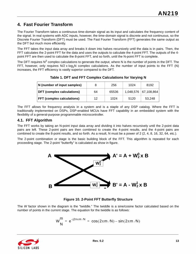
The 2-point combination or stage is the basic building block of the FFT. This algorithm is repeated for eachproceeding stage. The 2-point “butterfly” is calculated as show in figure.
Figure 10. 2-Point FFT Butterfly Structure
The W factor shown in the diagram is the “twiddle.” The twiddle is a sine/cosine factor calculated based on thenumber of points in the current stage. The equation for the twiddle is as follows:
Table 1. DFT and FFT Complex Calculations for Varying N
N (number of input samples) 8 256 1024 8192
DFT (complex calculations) 64 65536 1,048,576 67,108,864
FFT (complex calculations) 12 1024 5120 53,248
-
A
B
A' = A + W2 x B
B' = A - W2 x B1
W20
0
W21
Wm
Ne
j2nm– N2m N cos 2m N sin–= =
AN219
14 Rev. 0.2
where N is 2 for a 2-point stage and m is 0 to N-1 (so 0 and 1 in this case). Note that A and B are both complexnumbers, so they both contain real and imaginary components.
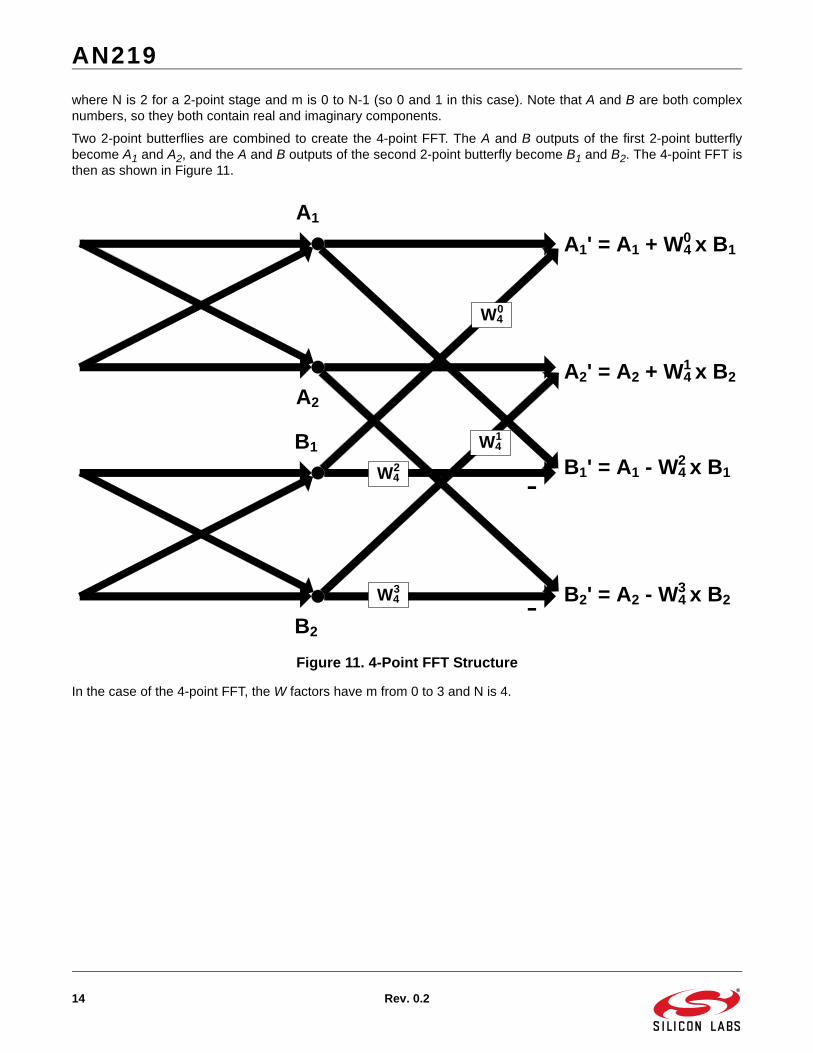
Two 2-point butterflies are combined to create the 4-point FFT. The A and B outputs of the first 2-point butterflybecome A1 and A2, and the A and B outputs of the second 2-point butterfly become B1 and B2. The 4-point FFT isthen as shown in Figure 11.
Figure 11. 4-Point FFT Structure
In the case of the 4-point FFT, the W factors have m from 0 to 3 and N is 4.
B2
B1
A1
A2
A1' = A1 + W4 x B1
A2' = A2 + W4 x B2
-B1' = A1 - W4 x B1
B2' = A2 - W4 x B2-
0
1
2
3
W40
W41
W42
W43
AN219
Rev. 0.2 15
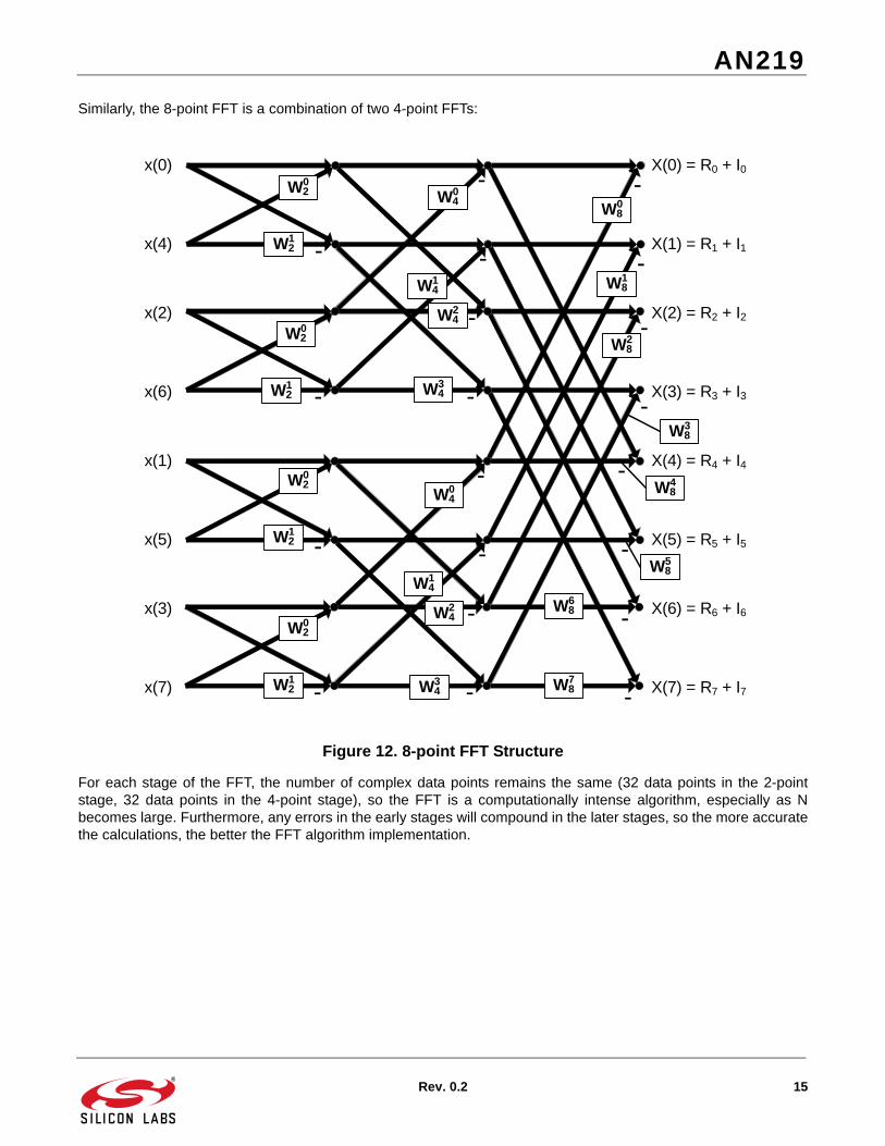
Similarly, the 8-point FFT is a combination of two 4-point FFTs:
Figure 12. 8-point FFT Structure
For each stage of the FFT, the number of complex data points remains the same (32 data points in the 2-pointstage, 32 data points in the 4-point stage), so the FFT is a computationally intense algorithm, especially as Nbecomes large. Furthermore, any errors in the early stages will compound in the later stages, so the more accuratethe calculations, the better the FFT algorithm implementation.
-
-
-
-
-
-
-
-
-
-
- -
-
-
-
-
-
-
-
-
x(0)
x(4)
x(2)
x(6)
x(1)
x(5)
x(3)
x(7)
X(0) = R0 + I0
X(1) = R1 + I1
X(2) = R2 + I2
X(3) = R3 + I3
X(4) = R4 + I4
X(5) = R5 + I5
X(6) = R6 + I6
X(7) = R7 + I7
W20
W21
W20
W21
W21
W20
W21
W20
W40
W41
W42
W43
W40
W41
W42
W43
W80
W81
W82
W83
W84
W85
W86
W87
AN219
16 Rev. 0.2
4.1.1. Windowing
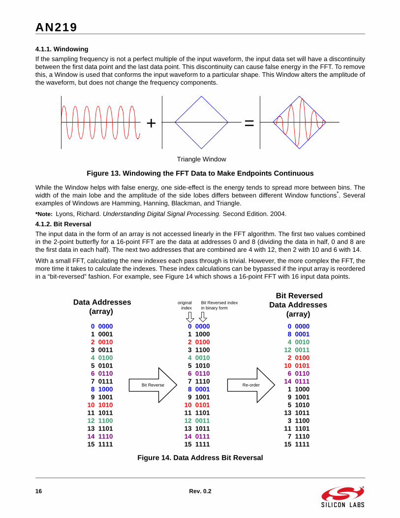
If the sampling frequency is not a perfect multiple of the input waveform, the input data set will have a discontinuitybetween the first data point and the last data point. This discontinuity can cause false energy in the FFT. To removethis, a Window is used that conforms the input waveform to a particular shape. This Window alters the amplitude ofthe waveform, but does not change the frequency components.
Figure 13. Windowing the FFT Data to Make Endpoints Continuous
While the Window helps with false energy, one side-effect is the energy tends to spread more between bins. Thewidth of the main lobe and the amplitude of the side lobes differs between different Window functions*. Severalexamples of Windows are Hamming, Hanning, Blackman, and Triangle.
*Note: Lyons, Richard. Understanding Digital Signal Processing. Second Edition. 2004.
4.1.2. Bit Reversal
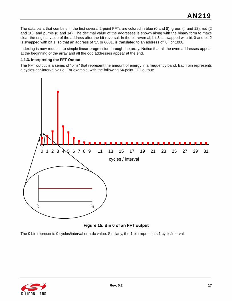
The input data in the form of an array is not accessed linearly in the FFT algorithm. The first two values combinedin the 2-point butterfly for a 16-point FFT are the data at addresses 0 and 8 (dividing the data in half, 0 and 8 arethe first data in each half). The next two addresses that are combined are 4 with 12, then 2 with 10 and 6 with 14.
With a small FFT, calculating the new indexes each pass through is trivial. However, the more complex the FFT, themore time it takes to calculate the indexes. These index calculations can be bypassed if the input array is reorderedin a “bit-reversed” fashion. For example, see Figure 14 which shows a 16-point FFT with 16 input data points.
Figure 14. Data Address Bit Reversal
+ =
Triangle Window
0 00001 00012 00103 00114 01005 01016 01107 01118 10009 1001
10 101011 101112 110013 110114 111015 1111
Data Addresses (array)
0 00008 00014 0010
12 00112 0100
10 01016 0110
14 01111 10009 10015 1010
13 10113 1100
11 11017 1110
15 1111
Bit Reversed Data Addresses
(array)
Re-order
0 00001 10002 01003 11004 00105 10106 01107 11108 00019 1001
10 010111 110112 001113 101114 011115 1111
Bit ReverseBit Reverse
original index
Bit Reversed index in binary form
AN219
Rev. 0.2 17
The data pairs that combine in the first several 2-point FFTs are colored in blue (0 and 8), green (4 and 12), red (2and 10), and purple (6 and 14). The decimal value of the addresses is shown along with the binary form to makeclear the original value of the address after the bit reversal. In the bit reversal, bit 3 is swapped with bit 0 and bit 2is swapped with bit 1, so that an address of ‘1’, or 0001, is translated to an address of ‘8’, or 1000.
Indexing is now reduced to simple linear progression through the array. Notice that all the even addresses appearat the beginning of the array and all the odd addresses appear at the end.
4.1.3. Interpreting the FFT Output
The FFT output is a series of “bins” that represent the amount of energy in a frequency band. Each bin representsa cycles-per-interval value. For example, with the following 64-point FFT output:
Figure 15. Bin 0 of an FFT output
The 0 bin represents 0 cycles/interval or a dc value. Similarly, the 1 bin represents 1 cycle/interval.
0 1 2 3 4 5 6 7 8 9 11 31292725232119171513
cycles / interval
t0 tN
AN219
18 Rev. 0.2
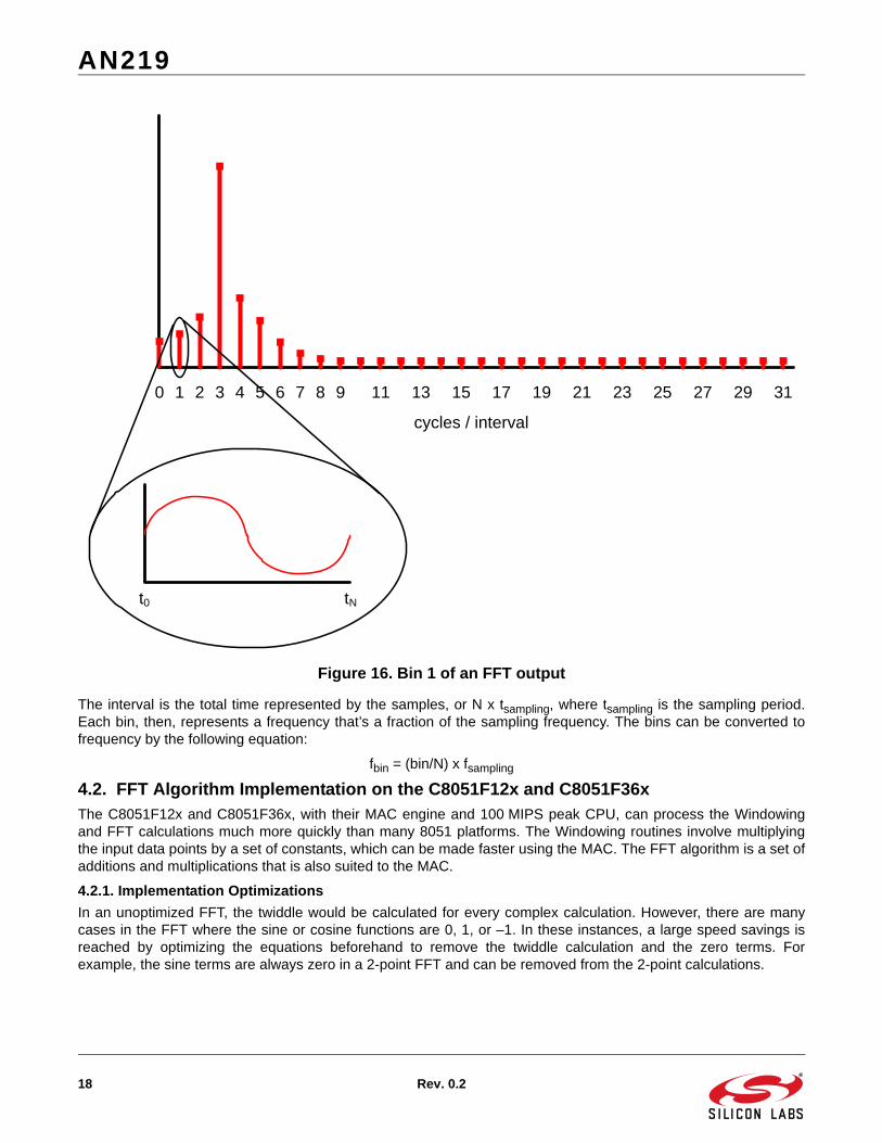
Figure 16. Bin 1 of an FFT output
The interval is the total time represented by the samples, or N x tsampling, where tsampling is the sampling period.Each bin, then, represents a frequency that’s a fraction of the sampling frequency. The bins can be converted tofrequency by the following equation:
fbin = (bin/N) x fsampling
4.2. FFT Algorithm Implementation on the C8051F12x and C8051F36xThe C8051F12x and C8051F36x, with their MAC engine and 100 MIPS peak CPU, can process the Windowingand FFT calculations much more quickly than many 8051 platforms. The Windowing routines involve multiplyingthe input data points by a set of constants, which can be made faster using the MAC. The FFT algorithm is a set ofadditions and multiplications that is also suited to the MAC.
4.2.1. Implementation Optimizations
In an unoptimized FFT, the twiddle would be calculated for every complex calculation. However, there are manycases in the FFT where the sine or cosine functions are 0, 1, or –1. In these instances, a large speed savings isreached by optimizing the equations beforehand to remove the twiddle calculation and the zero terms. Forexample, the sine terms are always zero in a 2-point FFT and can be removed from the 2-point calculations.
0 1 2 3 4 5 6 7 8 9 11 31292725232119171513
cycles / interval
t0 tN
AN219
Rev. 0.2 19
4.2.2. FFT Example
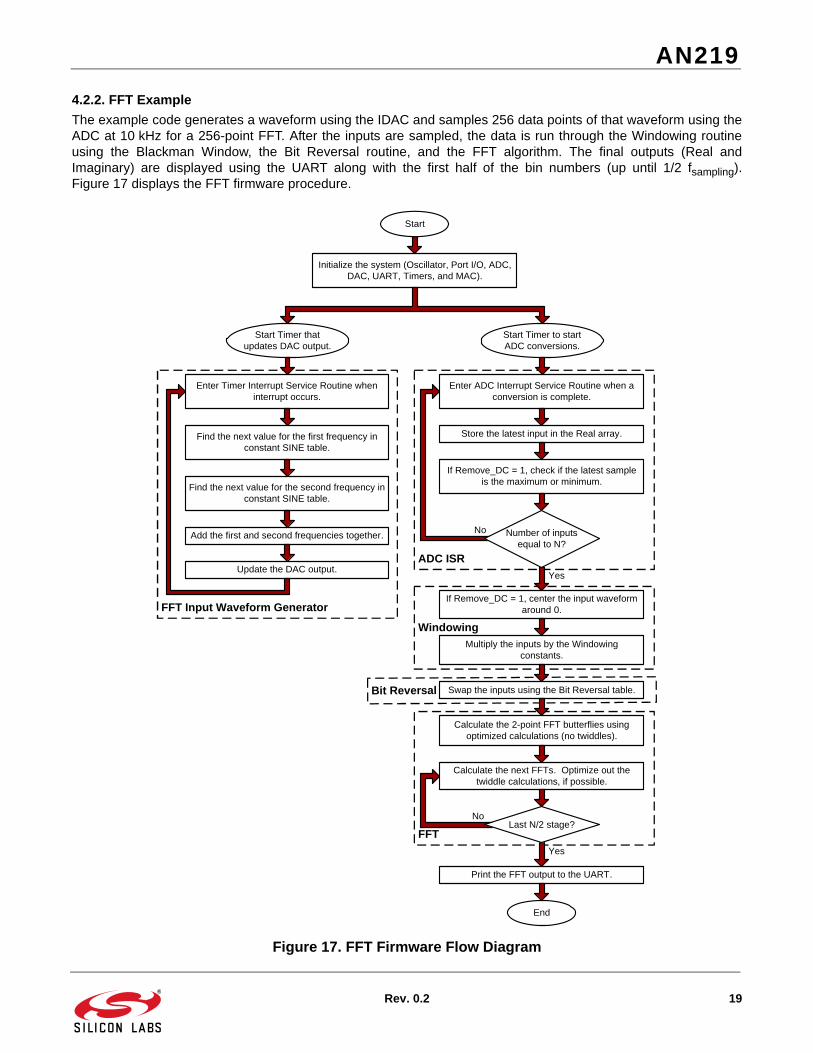
The example code generates a waveform using the IDAC and samples 256 data points of that waveform using theADC at 10 kHz for a 256-point FFT. After the inputs are sampled, the data is run through the Windowing routineusing the Blackman Window, the Bit Reversal routine, and the FFT algorithm. The final outputs (Real andImaginary) are displayed using the UART along with the first half of the bin numbers (up until 1/2 fsampling).Figure 17 displays the FFT firmware procedure.
Figure 17. FFT Firmware Flow Diagram
Initialize the system (Oscillator, Port I/O, ADC, DAC, UART, Timers, and MAC).
Start
Start Timer to start ADC conversions.
Start Timer that updates DAC output.
ADC ISR
FFT Input Waveform Generator
FFT
Windowing
Enter Timer Interrupt Service Routine when interrupt occurs.
Find the next value for the first frequency in constant SINE table.
Find the next value for the second frequency in constant SINE table.
Add the first and second frequencies together.
Update the DAC output.
Enter ADC Interrupt Service Routine when a conversion is complete.
Store the latest input in the Real array.
If Remove_DC = 1, center the input waveform around 0.
If Remove_DC = 1, check if the latest sample is the maximum or minimum.
No
Yes
Multiply the inputs by the Windowing constants.
Swap the inputs using the Bit Reversal table.
Calculate the 2-point FFT butterflies using optimized calculations (no twiddles).
Calculate the next FFTs. Optimize out the twiddle calculations, if possible.
No
Yes
End
Bit Reversal
Print the FFT output to the UART.
Number of inputs equal to N?
Last N/2 stage?
AN219
20 Rev. 0.2
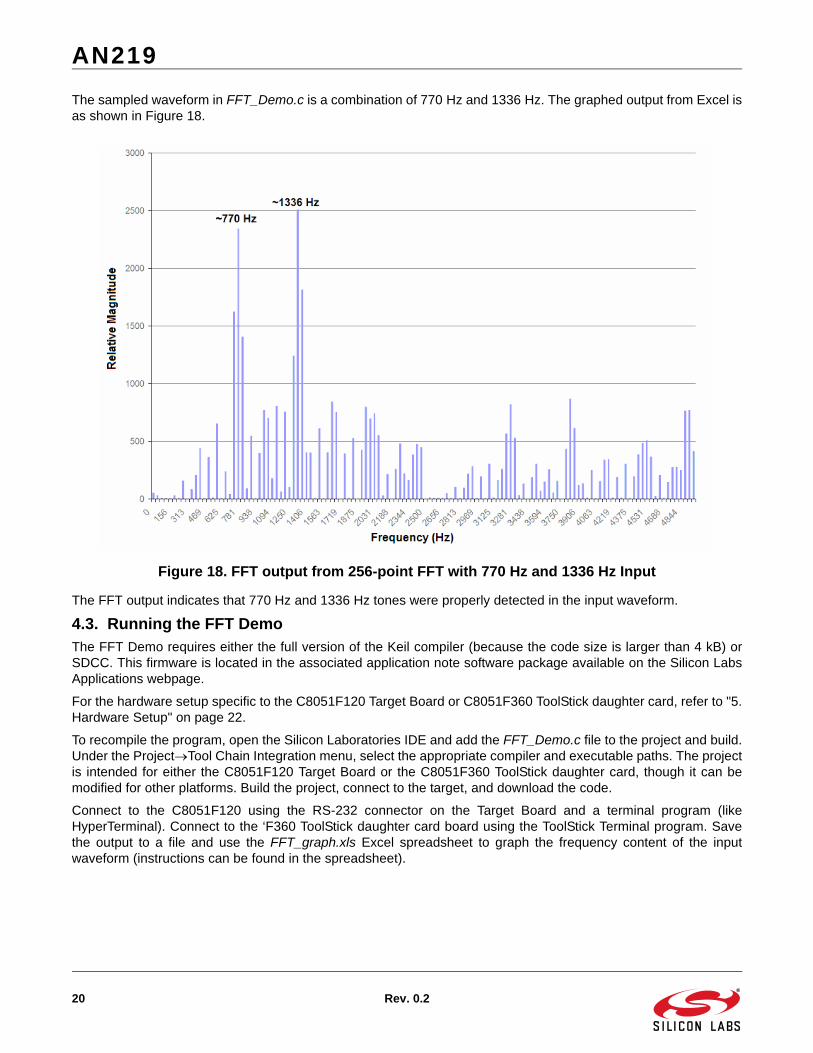
The sampled waveform in FFT_Demo.c is a combination of 770 Hz and 1336 Hz. The graphed output from Excel isas shown in Figure 18.
Figure 18. FFT output from 256-point FFT with 770 Hz and 1336 Hz Input
The FFT output indicates that 770 Hz and 1336 Hz tones were properly detected in the input waveform.
4.3. Running the FFT DemoThe FFT Demo requires either the full version of the Keil compiler (because the code size is larger than 4 kB) orSDCC. This firmware is located in the associated application note software package available on the Silicon LabsApplications webpage.
For the hardware setup specific to the C8051F120 Target Board or C8051F360 ToolStick daughter card, refer to "5.Hardware Setup" on page 22.
To recompile the program, open the Silicon Laboratories IDE and add the FFT_Demo.c file to the project and build.Under the ProjectTool Chain Integration menu, select the appropriate compiler and executable paths. The projectis intended for either the C8051F120 Target Board or the C8051F360 ToolStick daughter card, though it can bemodified for other platforms. Build the project, connect to the target, and download the code.
Connect to the C8051F120 using the RS-232 connector on the Target Board and a terminal program (likeHyperTerminal). Connect to the ‘F360 ToolStick daughter card board using the ToolStick Terminal program. Savethe output to a file and use the FFT_graph.xls Excel spreadsheet to graph the frequency content of the inputwaveform (instructions can be found in the spreadsheet).
AN219
Rev. 0.2 21
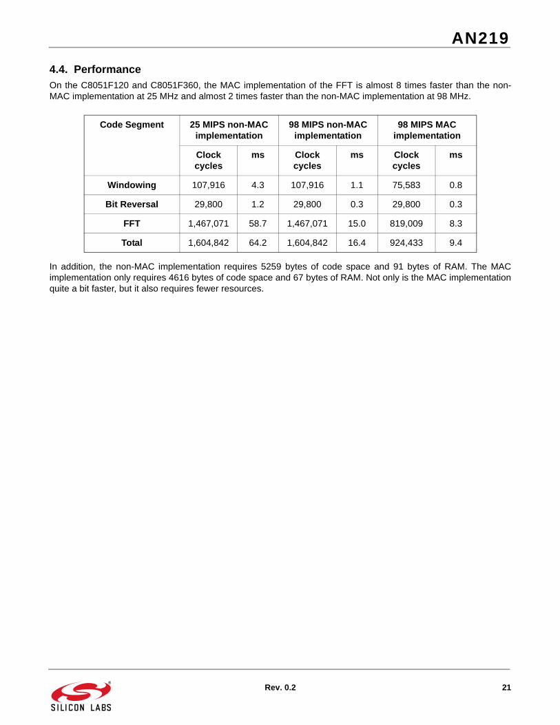
4.4. PerformanceOn the C8051F120 and C8051F360, the MAC implementation of the FFT is almost 8 times faster than the non-MAC implementation at 25 MHz and almost 2 times faster than the non-MAC implementation at 98 MHz.
In addition, the non-MAC implementation requires 5259 bytes of code space and 91 bytes of RAM. The MACimplementation only requires 4616 bytes of code space and 67 bytes of RAM. Not only is the MAC implementationquite a bit faster, but it also requires fewer resources.
Code Segment 25 MIPS non-MAC implementation
98 MIPS non-MAC implementation
98 MIPS MAC implementation
Clock cycles
ms Clock cycles
ms Clock cycles
ms
Windowing 107,916 4.3 107,916 1.1 75,583 0.8
Bit Reversal 29,800 1.2 29,800 0.3 29,800 0.3
FFT 1,467,071 58.7 1,467,071 15.0 819,009 8.3
Total 1,604,842 64.2 1,604,842 16.4 924,433 9.4
AN219
22 Rev. 0.2
5. Hardware Setup
The hardware setup descriptions apply to all of the different examples provided in this application note.
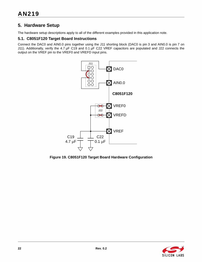
5.1. C8051F120 Target Board InstructionsConnect the DAC0 and AIN0.0 pins together using the J11 shorting block (DAC0 is pin 3 and AIN0.0 is pin 7 onJ11). Additionally, verify the 4.7 µF C19 and 0.1 µF C22 VREF capacitors are populated and J22 connects theoutput on the VREF pin to the VREF0 and VREFD input pins.
Figure 19. C8051F120 Target Board Hardware Configuration
J22
DAC0
AIN0.0
VREF0
VREFD
VREF
C8051F120
C194.7 µF
C220.1 µF
J11
AN219
Rev. 0.2 23
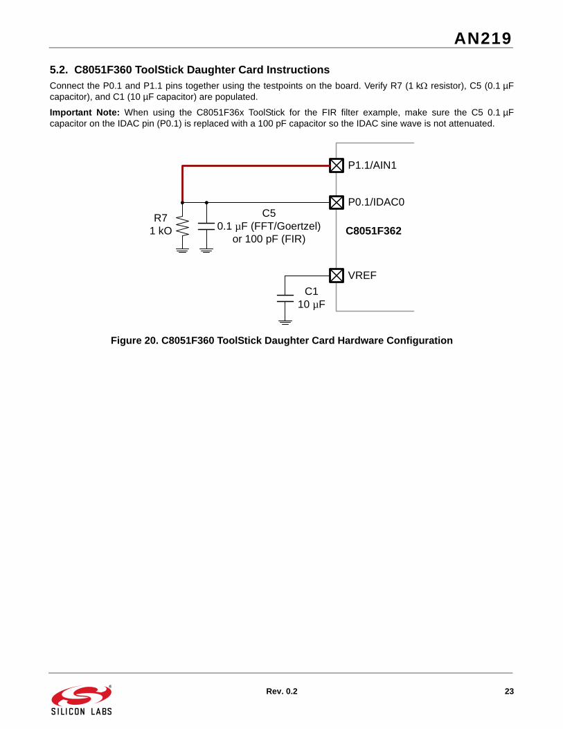
5.2. C8051F360 ToolStick Daughter Card InstructionsConnect the P0.1 and P1.1 pins together using the testpoints on the board. Verify R7 (1 k resistor), C5 (0.1 µFcapacitor), and C1 (10 µF capacitor) are populated.
Important Note: When using the C8051F36x ToolStick for the FIR filter example, make sure the C5 0.1 µFcapacitor on the IDAC pin (P0.1) is replaced with a 100 pF capacitor so the IDAC sine wave is not attenuated.
Figure 20. C8051F360 ToolStick Daughter Card Hardware Configuration
P1.1/AIN1
P0.1/IDAC0
VREF
C8051F362
C110 µF
C50.1 µF (FFT/Goertzel)
or 100 pF (FIR)
R71 kO

AN219
24 Rev. 0.2
DOCUMENT CHANGE LIST
Revision 0.1 to 0.2 Corrected table units in Section "2.3.1. Performance"
on page 7 and Section "3.4. Performance" on page 12.

http://www.silabs.com
Silicon Laboratories Inc.400 West Cesar ChavezAustin, TX 78701USA
Simplicity Studio
One-click access to MCU and wireless tools, documentation, software, source code libraries & more. Available for Windows, Mac and Linux!
IoT Portfoliowww.silabs.com/IoT
SW/HWwww.silabs.com/simplicity
Qualitywww.silabs.com/quality
Support and Communitycommunity.silabs.com
DisclaimerSilicon Labs intends to provide customers with the latest, accurate, and in-depth documentation of all peripherals and modules available for system and software implementers using or intending to use the Silicon Labs products. Characterization data, available modules and peripherals, memory sizes and memory addresses refer to each specific device, and "Typical" parameters provided can and do vary in different applications. Application examples described herein are for illustrative purposes only. Silicon Labs reserves the right to make changes without further notice and limitation to product information, specifications, and descriptions herein, and does not give warranties as to the accuracy or completeness of the included information. Silicon Labs shall have no liability for the consequences of use of the information supplied herein. This document does not imply or express copyright licenses granted hereunder to design or fabricate any integrated circuits. The products are not designed or authorized to be used within any Life Support System without the specific written consent of Silicon Labs. A "Life Support System" is any product or system intended to support or sustain life and/or health, which, if it fails, can be reasonably expected to result in significant personal injury or death. Silicon Labs products are not designed or authorized for military applications. Silicon Labs products shall under no circumstances be used in weapons of mass destruction including (but not limited to) nuclear, biological or chemical weapons, or missiles capable of delivering such weapons.
Trademark InformationSilicon Laboratories Inc.® , Silicon Laboratories®, Silicon Labs®, SiLabs® and the Silicon Labs logo®, Bluegiga®, Bluegiga Logo®, Clockbuilder®, CMEMS®, DSPLL®, EFM®, EFM32®, EFR, Ember®, Energy Micro, Energy Micro logo and combinations thereof, "the world’s most energy friendly microcontrollers", Ember®, EZLink®, EZRadio®, EZRadioPRO®, Gecko®, ISOmodem®, Precision32®, ProSLIC®, Simplicity Studio®, SiPHY®, Telegesis, the Telegesis Logo®, USBXpress® and others are trademarks or registered trademarks of Silicon Labs. ARM, CORTEX, Cortex-M3 and THUMB are trademarks or registered trademarks of ARM Holdings. Keil is a registered trademark of ARM Limited. All other products or brand names mentioned herein are trademarks of their respective holders.