user’s manual - mechatronic.net · user’s manual 8051 evaluation board ... picture 4-2. ax1.exe...
TRANSCRIPT

User’s Manual 8051 Evaluation Board
Copyright © 2001 WIZnet, Inc.
2
COPYRIGHT NOTICE
Copyright 2001 WIZnet, Inc. All Rights Reserved.
All information in this document is subject to change without notice.
Technical Support
E-mail : [email protected]
Phone : 82-2-6283-3500
Fax : 82-2-6283-3520
For other information, visit our websites at
http://www.i2Chip.com
3
Table of Contents Chapter 1. 8051 Evaluation Board Layout......................................... 8
1.1. Components ............................................................................ 8
1.2. MCU Section............................................................................ 9
1.3. Network Section....................................................................... 9
1.4. Power Section........................................................................ 10
1.5. Memory Section..................................................................... 11
1.5.1. Memory Map .......................................................... 11
1.6. PAL Source code ................................................................... 12
Chapter 2. Sample Code ................................................................. 14
2.1. Application Source Code ....................................................... 14
Chapter 3. Test Environment ........................................................... 15
3.1. System Set-up ....................................................................... 15
Chapter 4. Examples ....................................................................... 16
4.1. Loopback Test........................................................................ 16
4.1.1. Run Program from Flash ROM .............................. 16
4.1.2. Run Program from RAM......................................... 19
4.2. Testing with the Monitor program .......................................... 20
4.2.1. Test Procedures ..................................................... 20
4.2.2. Commands for the Monitor Program...................... 22
4.3. Web Server Test .................................................................... 27
4.3.1. Overview ................................................................ 27
4.3.2. Test Procedure ....................................................... 27
4.3.3. Description of Demo Web Page............................. 29
Chapter 5. User Application Development....................................... 31
5.1. Using 8051 Keil Compiler (uVision-51).................................. 31
4
5.2. Compile Options .................................................................... 31
5.2.1. ROM Specific Programs (Using ROM Writer) ........ 31
5.2.2. RAM Specific Programs ......................................... 34
Appendix A. 8051 EVB Board Package .................................................... 38
5
List of Pictures Picture 1-1. 8051 Evaluation Board.......................................................... 8
Picture 1-2. 8051EVB’s MCU Section ...................................................... 9
Picture 1-3. 8051EVB’s Network Section ............................................... 10
Picture 1-4. 8051EVB’s Power Section .................................................. 10
Picture 1-5. 8051EVB’s Memory Section ............................................... 11
Picture 1-6. Memory Map for 8051EVB.................................................. 12
Picture 2-1. Directory structure in 8051EVB CD .................................... 14
Picture 3-1. Test System Set-up............................................................. 15
Picture 4-1. Ping Test Command............................................................ 17
Picture 4-2. AX1.EXE Program .............................................................. 17
Picture 4-3. Connection Information Entry ............................................. 18
Picture 4-4. Connection Established ...................................................... 18
Picture 4-5. File Transfer ........................................................................ 18
Picture 4-6. Continuous Loopback Test.................................................. 19
Picture 4-7. 8051EVB Monitor Program’s Initial Screen ........................ 21
Picture 4-8. D Command Execution ....................................................... 23
Picture 4-9. Selecting Transfer Protocol................................................. 24
Picture 4-10. Upload Completed ............................................................ 25
Picture 4-11. R Command Execution ..................................................... 26
Picture 4-12. S Command Execution ..................................................... 27
Picture 4-13. 8051EVB Web Server Mode’s Initial Screen .................... 29
Picture 5-1. ROM Specific Start.a51 Example........................................ 32
Picture 5-2. ROM Specific Compiler Options ......................................... 33
Picture 5-3. ROM Specific Linker ........................................................... 34
Picture 5-4. RAM Specific Start.a51 Example ........................................ 35
6
Picture 5-5. RAM Specific Compiler Options.......................................... 36
Picture 5-6. RAM Specific Linker............................................................ 37

7
List of Tables Table 4-1. Values for Serial Port Connection.......................................... 21
Table 4-2. Quick Reference of Commands ............................................ 22
8
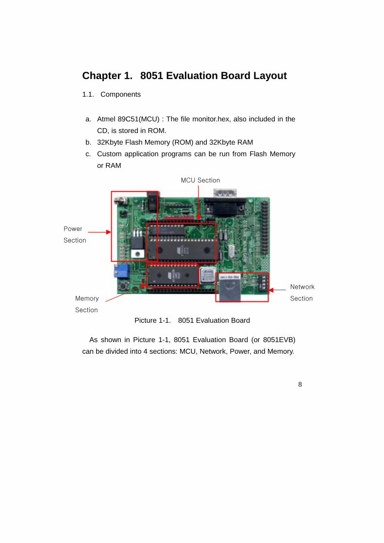
Chapter 1. 8051 Evaluation Board Layout 1.1. Components
a. Atmel 89C51(MCU) : The file monitor.hex, also included in the
CD, is stored in ROM. b. 32Kbyte Flash Memory (ROM) and 32Kbyte RAM c. Custom application programs can be run from Flash Memory
or RAM
Picture 1-1. 8051 Evaluation Board
As shown in Picture 1-1, 8051 Evaluation Board (or 8051EVB) can be divided into 4 sections: MCU, Network, Power, and Memory.
Power
Section
Memory
Section
MCU Section
Network
Section
9
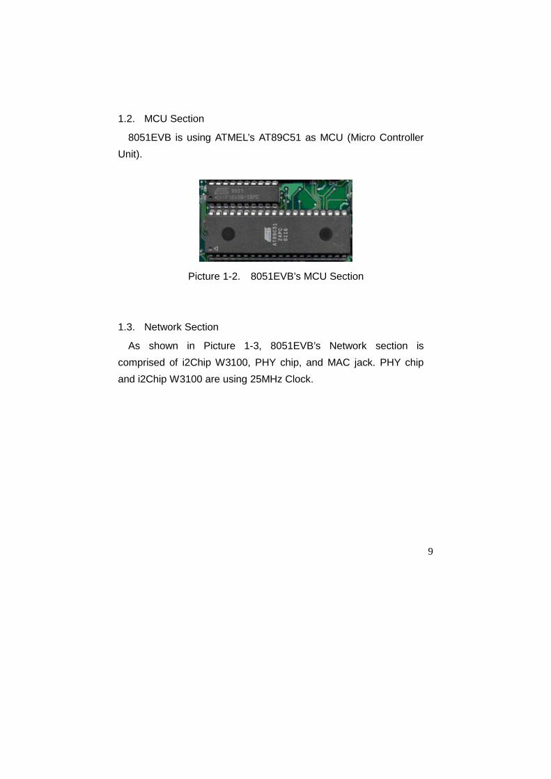
1.2. MCU Section
8051EVB is using ATMEL’s AT89C51 as MCU (Micro Controller Unit).
Picture 1-2. 8051EVB’s MCU Section
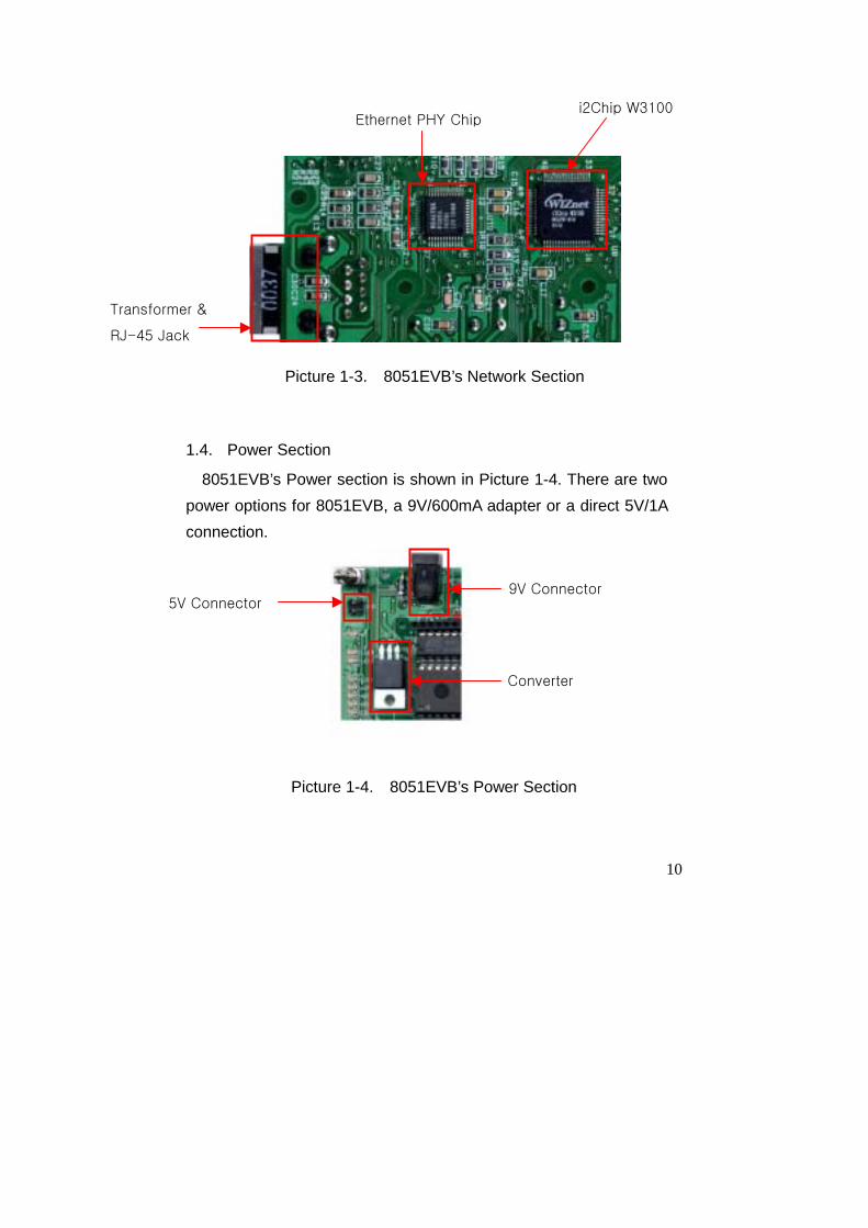
1.3. Network Section
As shown in Picture 1-3, 8051EVB’s Network section is comprised of i2Chip W3100, PHY chip, and MAC jack. PHY chip and i2Chip W3100 are using 25MHz Clock.
10
Picture 1-3. 8051EVB’s Network Section
1.4. Power Section
8051EVB’s Power section is shown in Picture 1-4. There are two power options for 8051EVB, a 9V/600mA adapter or a direct 5V/1A connection.
Picture 1-4. 8051EVB’s Power Section
Ethernet PHY Chip
Transformer &
RJ-45 Jack
i2Chip W3100
Converter
9V Connector 5V Connector
11
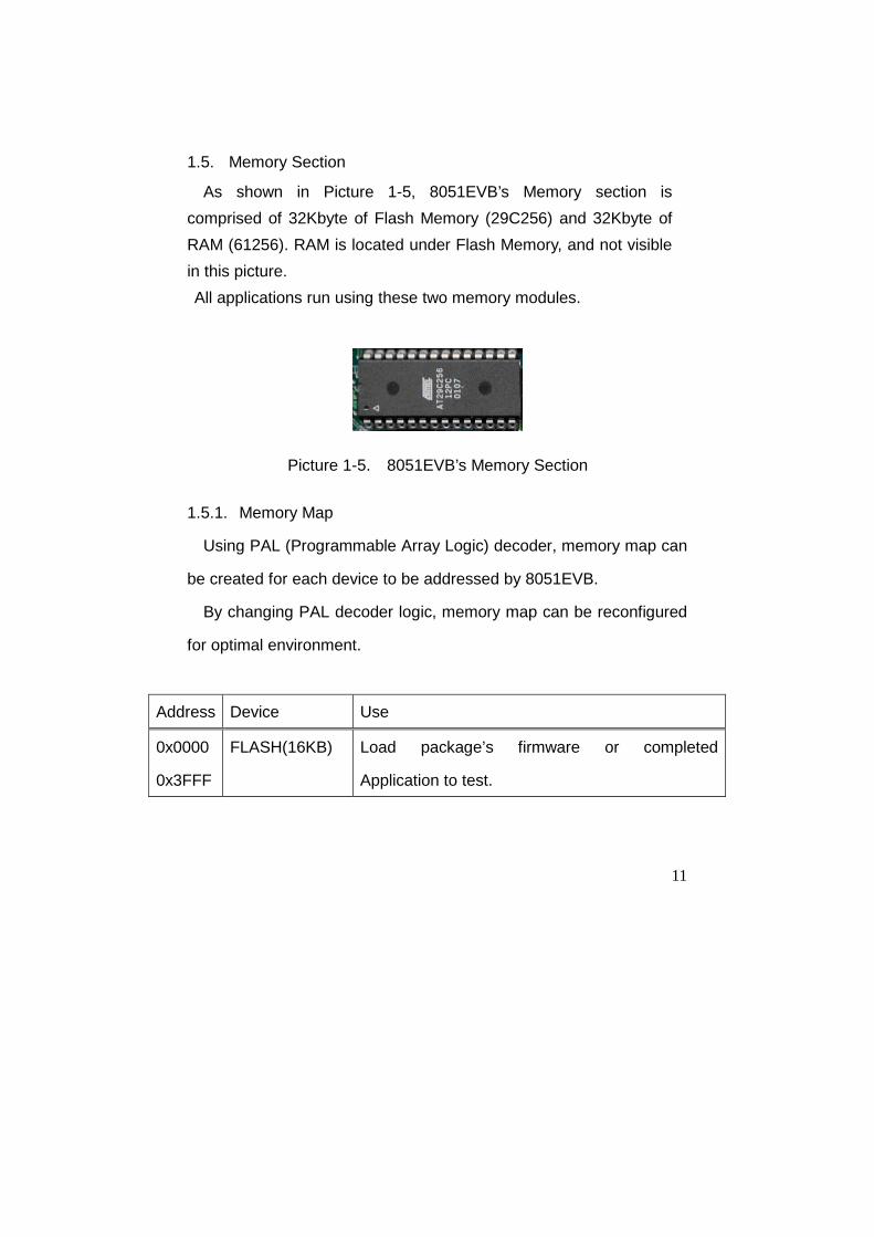
1.5. Memory Section
As shown in Picture 1-5, 8051EVB’s Memory section is comprised of 32Kbyte of Flash Memory (29C256) and 32Kbyte of RAM (61256). RAM is located under Flash Memory, and not visible in this picture. All applications run using these two memory modules.
Picture 1-5. 8051EVB’s Memory Section
1.5.1. Memory Map
Using PAL (Programmable Array Logic) decoder, memory map can
be created for each device to be addressed by 8051EVB.
By changing PAL decoder logic, memory map can be reconfigured
for optimal environment.
Address Device Use
0x0000
0x3FFF
FLASH(16KB) Load package’s firmware or completed
Application to test.
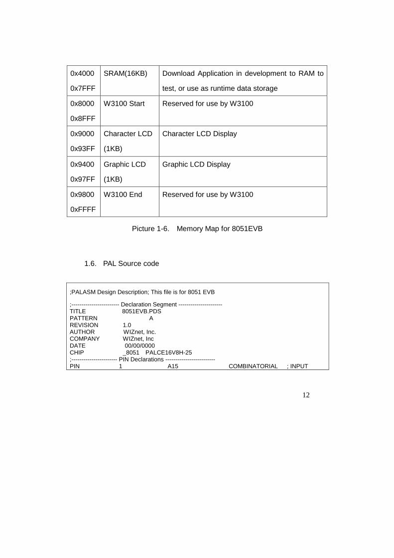
12
0x4000
0x7FFF
SRAM(16KB) Download Application in development to RAM to
test, or use as runtime data storage
0x8000
0x8FFF
W3100 Start Reserved for use by W3100
0x9000
0x93FF
Character LCD
(1KB)
Character LCD Display
0x9400
0x97FF
Graphic LCD
(1KB)
Graphic LCD Display
0x9800
0xFFFF
W3100 End Reserved for use by W3100
Picture 1-6. Memory Map for 8051EVB
1.6. PAL Source code
;PALASM Design Description; This file is for 8051 EVB
;------------------------ Declaration Segment ---------------------- TITLE 8051EVB.PDS PATTERN A REVISION 1.0 AUTHOR WIZnet, Inc. COMPANY WIZnet, Inc DATE 00/00/0000 CHIP _8051 PALCE16V8H-25 ;----------------------- PIN Declarations ------------------------- PIN 1 A15 COMBINATORIAL ; INPUT
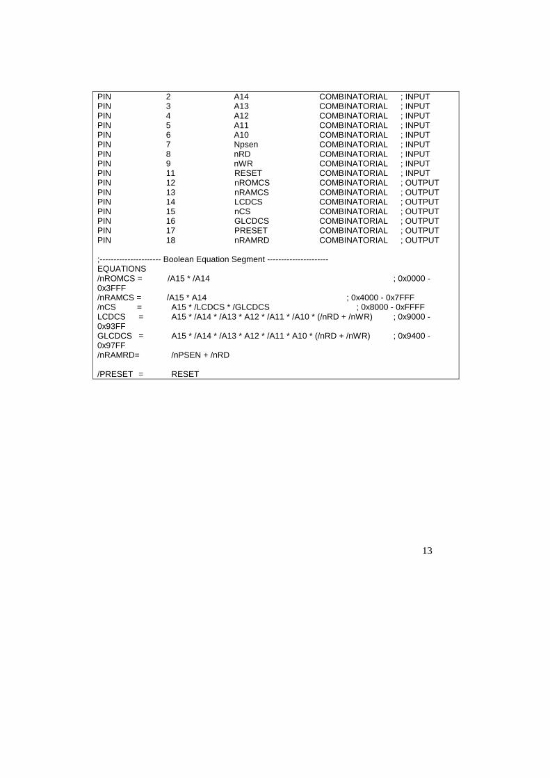
13
PIN 2 A14 COMBINATORIAL ; INPUT PIN 3 A13 COMBINATORIAL ; INPUT PIN 4 A12 COMBINATORIAL ; INPUT PIN 5 A11 COMBINATORIAL ; INPUT PIN 6 A10 COMBINATORIAL ; INPUT PIN 7 Npsen COMBINATORIAL ; INPUT PIN 8 nRD COMBINATORIAL ; INPUT PIN 9 nWR COMBINATORIAL ; INPUT PIN 11 RESET COMBINATORIAL ; INPUT PIN 12 nROMCS COMBINATORIAL ; OUTPUT PIN 13 nRAMCS COMBINATORIAL ; OUTPUT PIN 14 LCDCS COMBINATORIAL ; OUTPUT PIN 15 nCS COMBINATORIAL ; OUTPUT PIN 16 GLCDCS COMBINATORIAL ; OUTPUT PIN 17 PRESET COMBINATORIAL ; OUTPUT PIN 18 nRAMRD COMBINATORIAL ; OUTPUT ;---------------------- Boolean Equation Segment ---------------------- EQUATIONS /nROMCS = /A15 * /A14 ; 0x0000 - 0x3FFF /nRAMCS = /A15 * A14 ; 0x4000 - 0x7FFF /nCS = A15 * /LCDCS * /GLCDCS ; 0x8000 - 0xFFFF LCDCS = A15 * /A14 * /A13 * A12 * /A11 * /A10 * (/nRD + /nWR) ; 0x9000 - 0x93FF GLCDCS = A15 * /A14 * /A13 * A12 * /A11 * A10 * (/nRD + /nWR) ; 0x9400 - 0x97FF /nRAMRD= /nPSEN + /nRD /PRESET = RESET
14
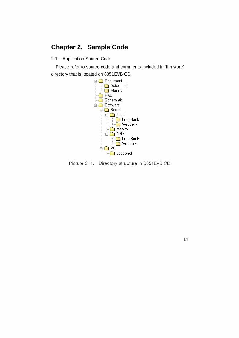
Chapter 2. Sample Code 2.1. Application Source Code
Please refer to source code and comments included in ‘firmware’ directory that is located on 8051EVB CD.
Picture 2-1. Directory structure in 8051EVB CD
15
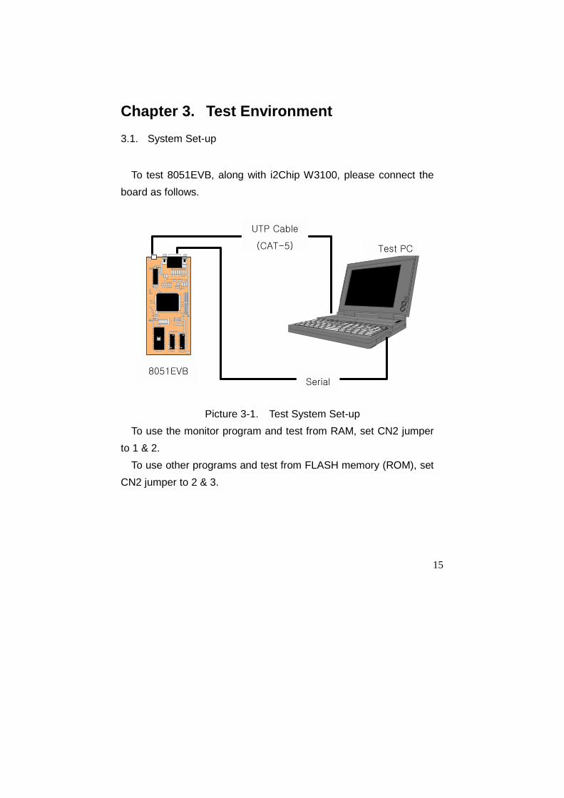
Chapter 3. Test Environment 3.1. System Set-up
To test 8051EVB, along with i2Chip W3100, please connect the
board as follows.
Picture 3-1. Test System Set-up To use the monitor program and test from RAM, set CN2 jumper
to 1 & 2. To use other programs and test from FLASH memory (ROM), set
CN2 jumper to 2 & 3.
Serial
UTP Cable
(CAT-5)
8051EVB
Test PC
16
Chapter 4. Examples 4.1. Loopback Test
4.1.1. Run Program from Flash ROM
Loopback program is used to test communication capability of i2Chip W3100 on 8051EVB. Communication speed test is performed by sending data from PC to 8051EVB, then having 8051EVB send the received data back to PC.
4.1.1.1. Test Environment The Loopback program has been pre-loaded into Flash ROM as
default application, to facilitate immediate testing of 8051EVB board without additional effort spent for set-up.
First, install Axinstall.EXE (located on CD, in directory Software\PC\Loopback\) on the PC. The set-up program will create a new application, called AX1.EXE, needed to run Loopback test.
To test a new program from Flash ROM, set the CN2 jumper to 2 & 3, and then download the program (start from memory address at 0x0000) using ROM Writer. Connect power, Serial and UTP cables, before powering up. The program can be monitored using HyperTerminal from PC. Use Reset key on 8051EVB board in case of initial difficulty. 4.1.1.2. Loopback Test Procedures ① Set CN2 jumper to 2 & 3
17
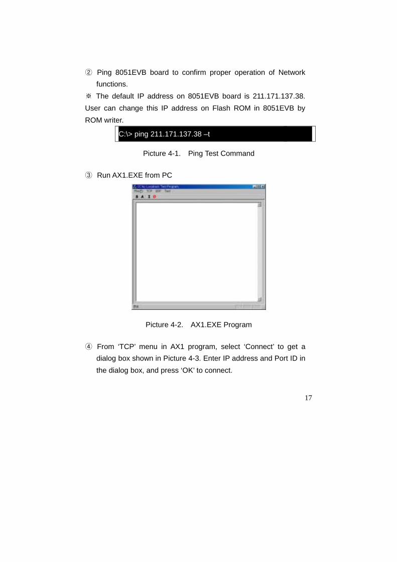
② Ping 8051EVB board to confirm proper operation of Network functions.
※ The default IP address on 8051EVB board is 211.171.137.38. User can change this IP address on Flash ROM in 8051EVB by ROM writer.
C:\> ping 211.171.137.38 –t
Picture 4-1. Ping Test Command
③ Run AX1.EXE from PC
Picture 4-2. AX1.EXE Program
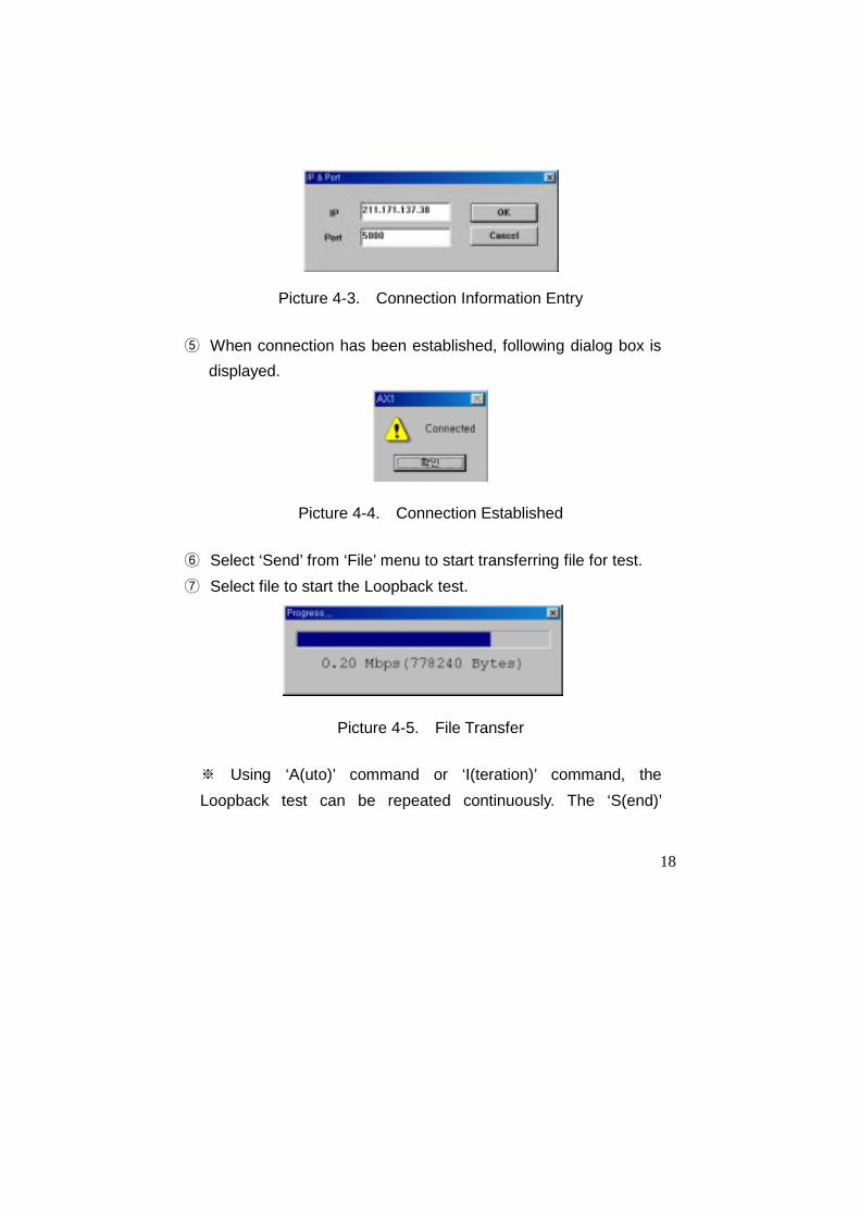
④ From ‘TCP’ menu in AX1 program, select ‘Connect’ to get a dialog box shown in Picture 4-3. Enter IP address and Port ID in the dialog box, and press ‘OK’ to connect.
18
Picture 4-3. Connection Information Entry
⑤ When connection has been established, following dialog box is displayed.
Picture 4-4. Connection Established
⑥ Select ‘Send’ from ‘File’ menu to start transferring file for test. ⑦ Select file to start the Loopback test.
Picture 4-5. File Transfer
※ Using ‘A(uto)’ command or ‘I(teration)’ command, the Loopback test can be repeated continuously. The ‘S(end)’
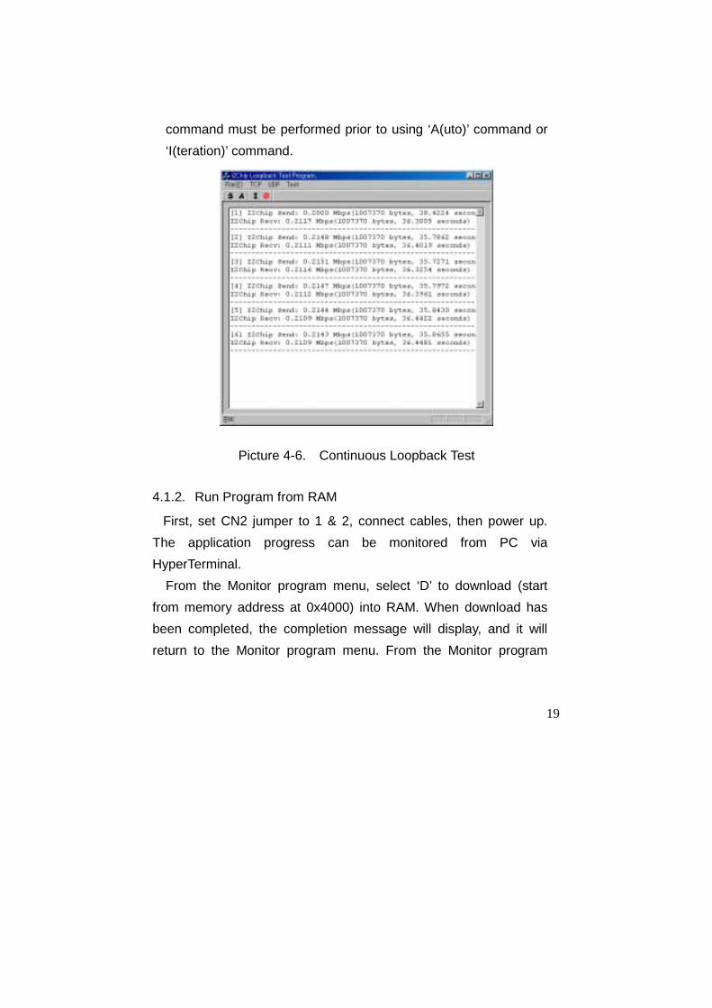
19
command must be performed prior to using ‘A(uto)’ command or ‘I(teration)’ command.
Picture 4-6. Continuous Loopback Test
4.1.2. Run Program from RAM
First, set CN2 jumper to 1 & 2, connect cables, then power up. The application progress can be monitored from PC via HyperTerminal.
From the Monitor program menu, select ‘D’ to download (start from memory address at 0x4000) into RAM. When download has been completed, the completion message will display, and it will return to the Monitor program menu. From the Monitor program
20
menu, select ‘R’ to run downloaded program (refer to 4.2 for procedures to test using the Monitor program).
4.2. Testing with the Monitor program
The Monitor program is included with 8051EVB board to aid development. The Monitor program allows the developer to load their custom program into SRAM to test, and at the same time, monitors memory usage.
The Monitor program communicates with PC through Serial Port connection. A Serial cable (cross cable) is included in the 8051EVB package.
4.2.1. Test Procedures
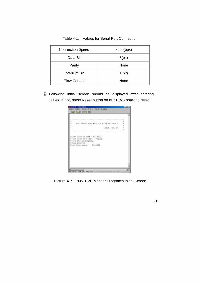
① Connect 8051EVB to PC using a Serial cable. Open HyperTerminal provided by Windows OS (other similar programs, i.e. Serome’s DataMan, can be used in place of HyperTerminal).
② Set 8051EVB’s CN2 jumper to 1 & 2, then press reset button. ③ Following Table 4.1 lists values used for session connection.
21
Table 4-1. Values for Serial Port Connection
Connection Speed 9600(bps)
Data Bit 8(bit)
Parity None
Interrupt Bit 1(bit)
Flow Control None
④ Following initial screen should be displayed after entering
values. If not, press Reset button on 8051EVB board to reset.
Picture 4-7. 8051EVB Monitor Program’s Initial Screen
22
The board is now ready to run developer’s custom program using
options provided.
4.2.2. Commands for the Monitor Program
The following 5 commands are provided with 8051EVB Monitor program.
Table 4-2. Quick Reference of Commands
CMD Description
D Download program to RAM at 0x4000 (HEX파일)
F Download program to FLASH ROM
P Display Port status
R Run program from RAM
S Memory dump from 64 Byte Address
※ These commands are case sensitive. Use capital letters. ※ ‘F’ command is not supported currently.
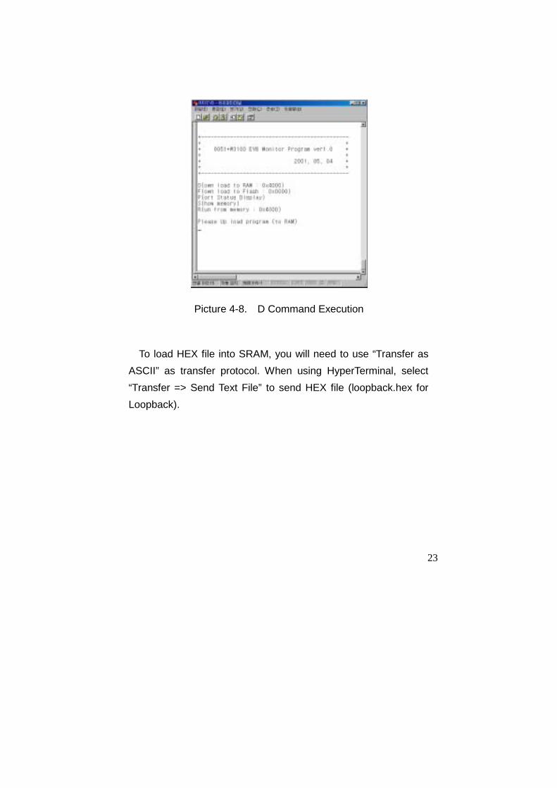
4.2.2.1. D Command
To test HEX file during development, use this command to load program into SRAM. When D command is entered from Command Prompt, “Please Up load program (to RAM)” message will be displayed as shown below.
23
Picture 4-8. D Command Execution
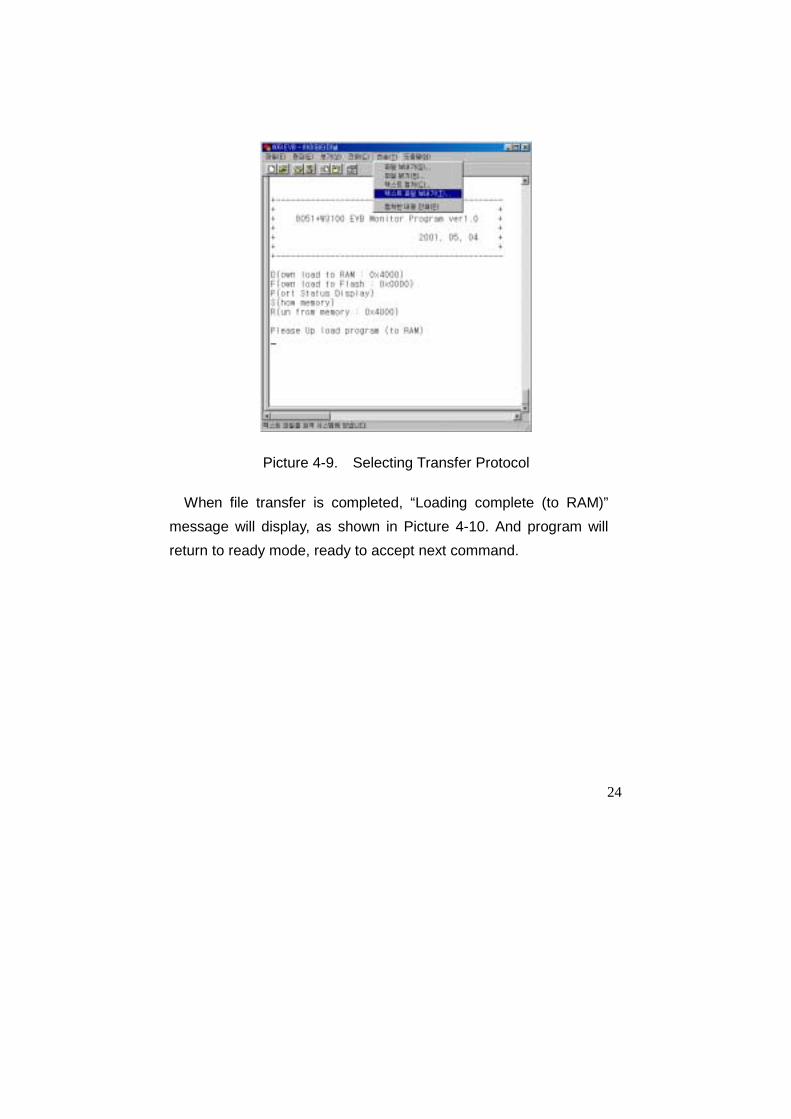
To load HEX file into SRAM, you will need to use “Transfer as
ASCII” as transfer protocol. When using HyperTerminal, select “Transfer => Send Text File” to send HEX file (loopback.hex for Loopback).
24
Picture 4-9. Selecting Transfer Protocol
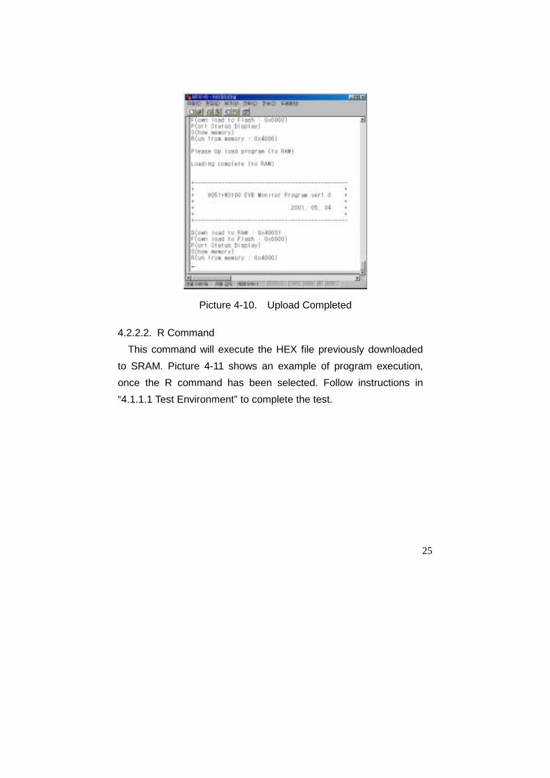
When file transfer is completed, “Loading complete (to RAM)” message will display, as shown in Picture 4-10. And program will return to ready mode, ready to accept next command.
25
Picture 4-10. Upload Completed
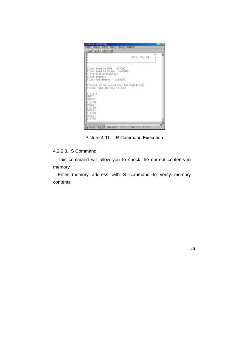
4.2.2.2. R Command This command will execute the HEX file previously downloaded
to SRAM. Picture 4-11 shows an example of program execution, once the R command has been selected. Follow instructions in “4.1.1.1 Test Environment” to complete the test.
26
Picture 4-11. R Command Execution
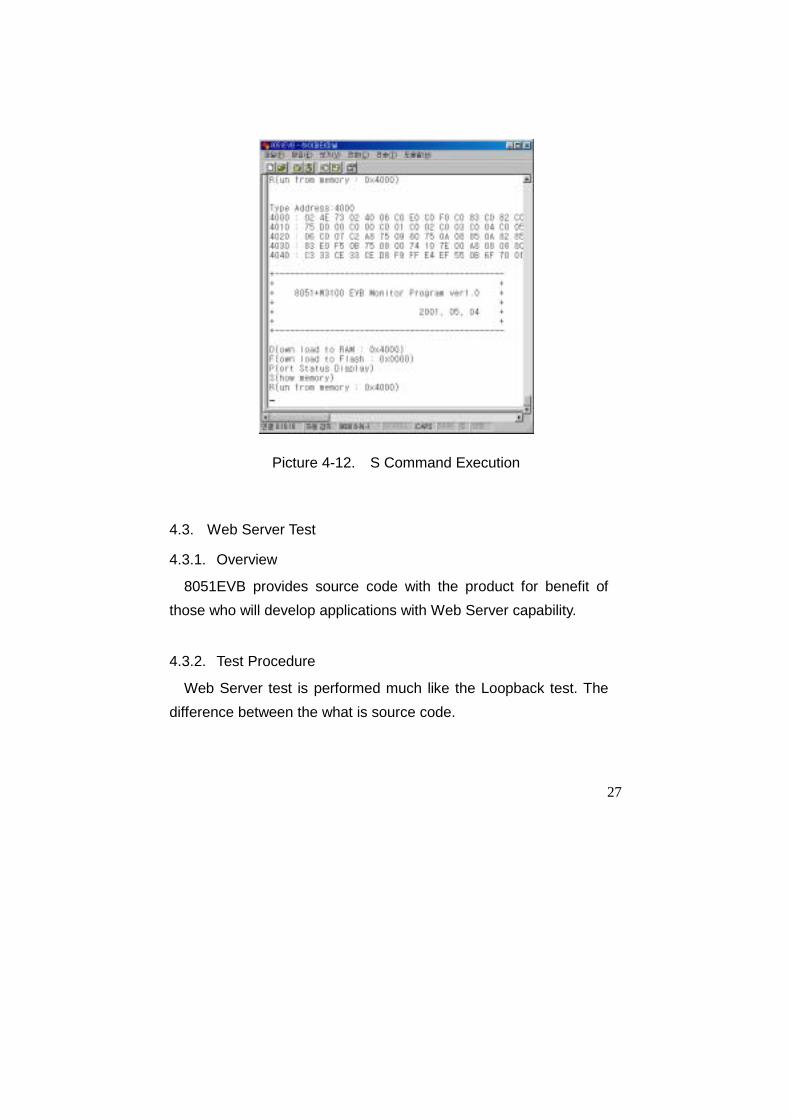
4.2.2.3. S Command
This command will allow you to check the current contents in memory.
Enter memory address with S command to verify memory contents.
27
Picture 4-12. S Command Execution
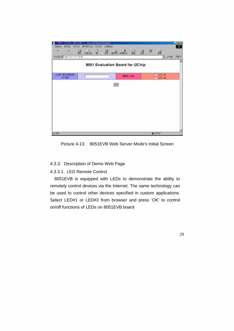
4.3. Web Server Test
4.3.1. Overview
8051EVB provides source code with the product for benefit of those who will develop applications with Web Server capability.
4.3.2. Test Procedure
Web Server test is performed much like the Loopback test. The difference between the what is source code.
28
(1) To run the program from Flash ROM for testing, set CN2 jumper to 2 & 3, then load Webserv.HEX (located in CD provided, in “Software/Board/Flash/webserv” directory) into Flash ROM using the ROM Writer. (2) To run the program from RAM using the Monitor program, set CN2 jumper to 1 & 2, then load Webserv.HEX (located in CD provided, in “Software/Board/Ram/webserv” directory) into RAM using the Monitor program.
① To verify Network connection, perform Ping test. The default IP
address for 8051EVB board is set to 211.171.137.38. ② From PC, start the Browser program. Enter IP address for
8051EVB to initiate communication. ③ Following initial screen will display on your browser with proper
connection under the Web Server mode.
29
Picture 4-13. 8051EVB Web Server Mode’s Initial Screen
4.3.3. Description of Demo Web Page
4.3.3.1. LED Remote Control 8051EVB is equipped with LEDs to demonstrate the ability to
remotely control devices via the Internet. The same technology can be used to control other devices specified in custom applications. Select LED#1 or LED#2 from browser and press ‘OK’ to control on/off functions of LEDs on 8051EVB board
30
4.3.3.2. LCD Text Display Function
Enter some text into LCD Text Box in demo web page. The text will
be displayed on LCD of 8051EVB. The LCD must be installed
separately.

31
Chapter 5. User Application Development 5.1. Using 8051 Keil Compiler (uVision-51)
1) Run uVision-51 2) From “Project” menu, create new project 3) Copy “c51.h” and “startup.a51” files to project created 4) From “Project” menu’s “edit project”, add source and
startup.a51 file. From “Option” menu, select “C51 compiler option”. Then from “listing” tab, add “symbols” and “assembly code”
5) From “Option” menu, select “BL51 Code Banking Linker”. Then from “Size/Location” tab, specify value for “Xdata address” (hex)
6) From “Option” menu, select “make”. Then from “Misc” tab, check “Ignore Warnings” option
7) Build
5.2. Compile Options
5.2.1. ROM Specific Programs (Using ROM Writer)
From Software/Board/Flash/LoopBack/startup.a51, find “CSEG AT“, and adjust Code Segment address to start from 0x0000.
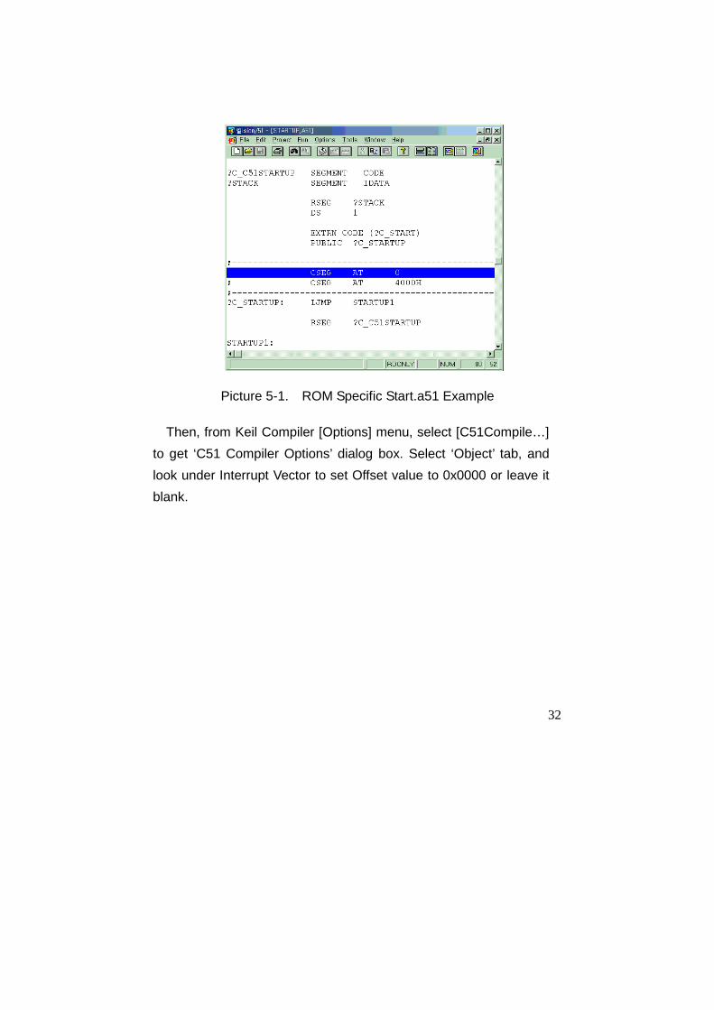
32
Picture 5-1. ROM Specific Start.a51 Example
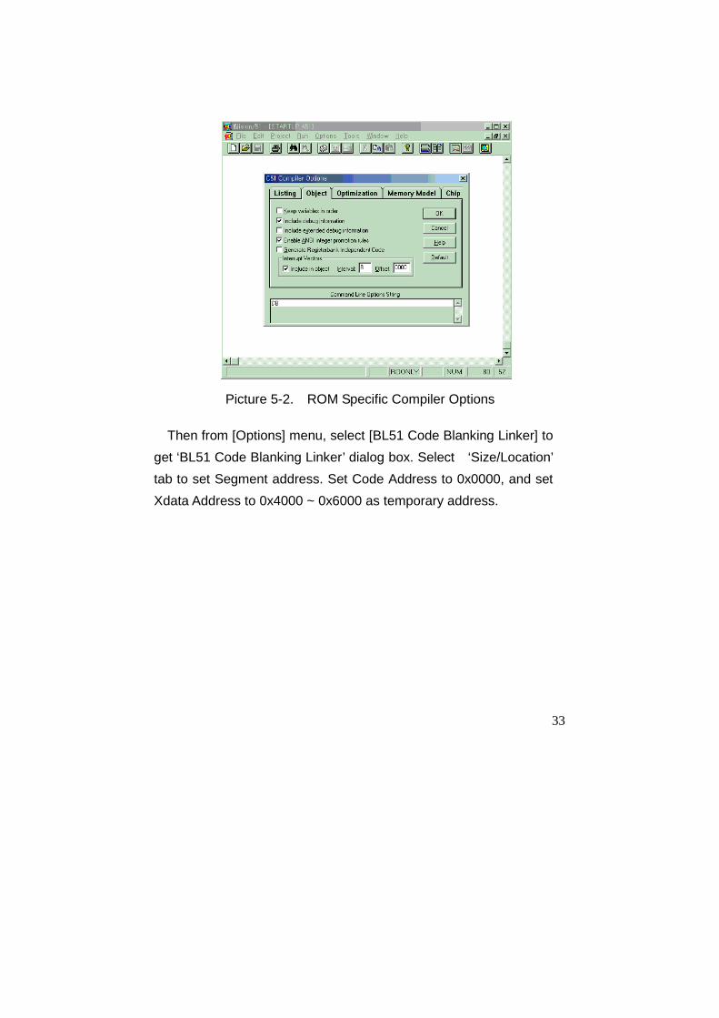
Then, from Keil Compiler [Options] menu, select [C51Compile…] to get ‘C51 Compiler Options’ dialog box. Select ‘Object’ tab, and look under Interrupt Vector to set Offset value to 0x0000 or leave it blank.
33
Picture 5-2. ROM Specific Compiler Options
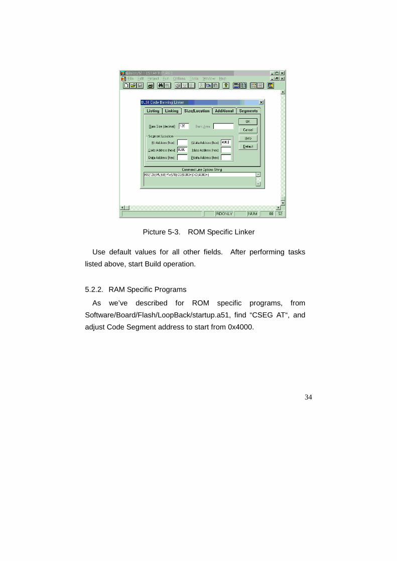
Then from [Options] menu, select [BL51 Code Blanking Linker] to get ‘BL51 Code Blanking Linker’ dialog box. Select ‘Size/Location’ tab to set Segment address. Set Code Address to 0x0000, and set Xdata Address to 0x4000 ~ 0x6000 as temporary address.
34
Picture 5-3. ROM Specific Linker
Use default values for all other fields. After performing tasks listed above, start Build operation.
5.2.2. RAM Specific Programs
As we’ve described for ROM specific programs, from Software/Board/Flash/LoopBack/startup.a51, find “CSEG AT“, and adjust Code Segment address to start from 0x4000.
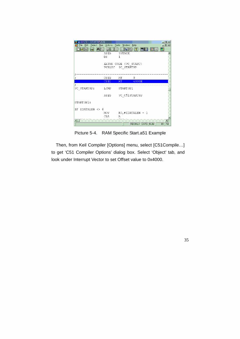
35
Picture 5-4. RAM Specific Start.a51 Example
Then, from Keil Compiler [Options] menu, select [C51Compile…] to get ‘C51 Compiler Options’ dialog box. Select ‘Object’ tab, and look under Interrupt Vector to set Offset value to 0x4000.
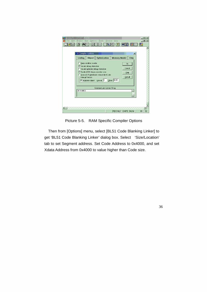
36
Picture 5-5. RAM Specific Compiler Options
Then from [Options] menu, select [BL51 Code Blanking Linker] to get ‘BL51 Code Blanking Linker’ dialog box. Select ‘Size/Location’ tab to set Segment address. Set Code Address to 0x4000, and set Xdata Address from 0x4000 to value higher than Code size.
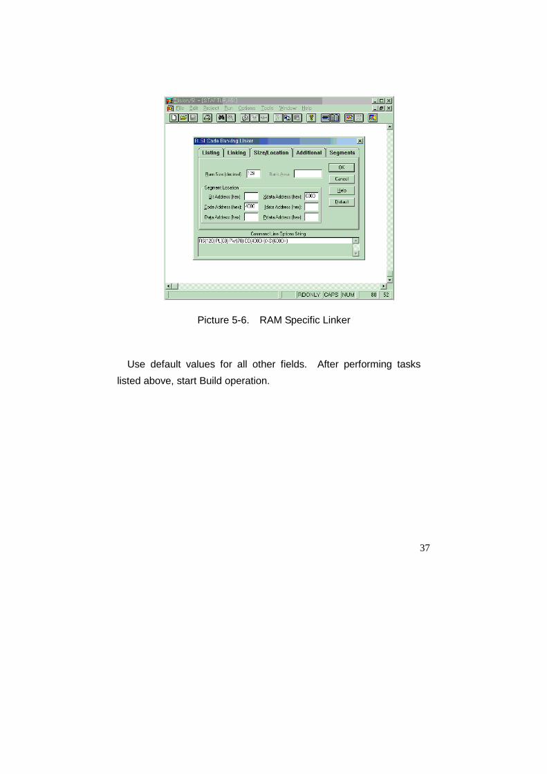
37
Picture 5-6. RAM Specific Linker
Use default values for all other fields. After performing tasks
listed above, start Build operation.
38
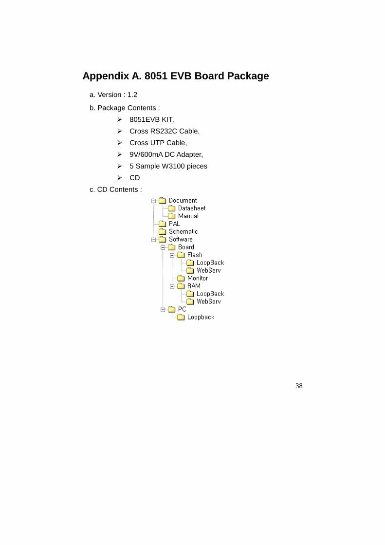
Appendix A. 8051 EVB Board Package a. Version : 1.2
b. Package Contents : ! 8051EVB KIT, ! Cross RS232C Cable, ! Cross UTP Cable, ! 9V/600mA DC Adapter, ! 5 Sample W3100 pieces ! CD
c. CD Contents :
39
d. Additional Tools Needed : ! 8051 Keil Compiler ! Communication Program (HyperTerminal, Serome
DataMan, etc...)