user manual mio-2260 - elmarksupport.elmark.com.pl/advantech/pdf/mio-2260_man.pdf · user manual...
TRANSCRIPT

User Manual
MIO-2260
MI/O-Ultra SBC with Intel® Atom™ N455, DDR3, 18-bit LVDS, VGA, GbE, Mini PCIe, 2 COM, 2 USB, MIOe

CopyrightThe documentation and the software included with this product are copyrighted 2011by Advantech Co., Ltd. All rights are reserved. Advantech Co., Ltd. reserves the rightto make improvements in the products described in this manual at any time withoutnotice.
No part of this manual may be reproduced, copied, translated or transmitted in anyform or by any means without the prior written permission of Advantech Co., Ltd.Information provided in this manual is intended to be accurate and reliable. However,Advantech Co., Ltd. assumes no responsibility for its use, nor for any infringementsof the rights of third parties, which may result from its use.
AcknowledgementsAMI is a trademark of AMI Software International, Inc.
Intel® is a trademark of Intel® Technologies, Inc.
IBM, PC/AT, PS/2 and VGA are trademarks of International Business Machines Cor-poration.
Intel and Atom® are trademarks of Intel Corporation.
Microsoft Windows® is a registered trademark of Microsoft Corp.
RTL is a trademark of Realtek Semi-Conductor Co., Ltd.
ESS is a trademark of ESS Technology, Inc.
UMC is a trademark of United Microelectronics Corporation.
SMI is a trademark of Silicon Motion, Inc.
Creative is a trademark of Creative Technology LTD.
All other product names or trademarks are properties of their respective owners.
Part No. 2006226010 Edition 1
Printed in China November 2011
MIO-2260 User Manual ii

Product Warranty (2 years)Advantech warrants to you, the original purchaser, that each of its products will befree from defects in materials and workmanship for two years from the date of pur-chase.
This warranty does not apply to any products which have been repaired or altered bypersons other than repair personnel authorized by Advantech, or which have beensubject to misuse, abuse, accident or improper installation. Advantech assumes noliability under the terms of this warranty as a consequence of such events.
Because of Advantech’s high quality-control standards and rigorous testing, most ofour customers never need to use our repair service. If an Advantech product is defec-tive, it will be repaired or replaced at no charge during the warranty period. For out-of-warranty repairs, you will be billed according to the cost of replacement materials,service time and freight. Please consult your dealer for more details.
If you think you have a defective product, follow these steps:
1. Collect all the information about the problem encountered. (For example, CPU speed, Advantech products used, other hardware and software used, etc.) Note anything abnormal and list any onscreen messages you get when the problem occurs.
2. Call your dealer and describe the problem. Please have your manual, product, and any helpful information readily available.
3. If your product is diagnosed as defective, obtain an RMA (return merchandize authorization) number from your dealer. This allows us to process your return more quickly.
4. Carefully pack the defective product, a fully-completed Repair and Replacement Order Card and a photocopy proof of purchase date (such as your sales receipt) in a shippable container. A product returned without proof of the purchase date is not eligible for warranty service.
5. Write the RMA number visibly on the outside of the package and ship it prepaid to your dealer.
Technical Support and Assistance1. Visit the Advantech web site at www.advantech.com/support where you can find
the latest information about the product.2. Contact your distributor, sales representative, or Advantech's customer service
center for technical support if you need additional assistance. Please have the following information ready before you call:– Product name and serial number– Description of your peripheral attachments– Description of your software (operating system, version, application software,
etc.)– A complete description of the problem– The exact wording of any error messages
iii MIO-2260 User Manual
Packing ListBefore installation, please ensure the following items have been shipped:
Item Part Number
1 MIO-2260 SBC 1 Startup manual 1 Utility CD Cables
Heatsink:
Stud & Screw
Ordering informationModel Number Description
Optional accessoriesPart No. Description
1960053176N001 Heat Spreader (99.5 x 70.5 x 11.2 mm)
Part Number Description
1700006291 SATA cable 7P 30 cm w/ right angle
1700019156 Audio Cable 2*5P-2.0/JACK*2 20cm
1701200220 COM PORT cable 2*10P-2.0/D-SUB 9P(M)*2 22 cm
1700019656 SATA Power cable 5P-1.25/5P-2.0+SATA 5P 15 cm
1960053175T001 99.5x70.5x15.7mm
Part Number Description
1910002088 Stud F=M3*10L M=M3*5L B=5 H=16, 4pcs
1935032000 Screw R/S 5.5 2.0 +M M3*20L, 4pcs
193B0204C0 Screw F/S D=3.5 H=0.8 + M2*4L, 1pcs
MIO-2260NF-S6A1E Atom N455, fanless, 12V, VGA, LVDS, GbE, 2 USB, MIOe
MIO-2260 User Manual iv

Certification and Safety InstructionsThis device complies with the requirements in part 15 of the FCC rules: Operation issubject to the following two conditions:
1. This device may not cause harmful interference, and2. This device must accept any interference received, including interference that
may cause undesired operation
This equipment has been tested and found to comply with the limits for a Class A dig-ital device, pursuant to Part 15 of the FCC Rules. These limits are designed to pro-vide reasonable protection against harmful interference when the equipment isoperated in a commercial environment. This equipment generates, uses, and canradiate radio frequency energy and, if not installed and used in accordance with theinstruction manual, may cause harmful interference to radio communications. Opera-tion of this device in a residential area is likely to cause harmful interference in whichcase the user will be required to correct the interference at his/her own expense. Theuser is advised that any equipment changes or modifications not expressly approvedby the party responsible for compliance would void the compliance to FCC regula-tions and therefore, the user's authority to operate the equipment.
Caution! There is a danger of a new battery exploding if it is incorrectly installed. Do not attempt to recharge, force open, or heat the battery. Replace the battery only with the same or equivalent type recommended by the man-ufacturer. Discard used batteries according to the manufacturer's instructions.
v MIO-2260 User Manual

MIO-2260 User Manual vi

Contents
Chapter 1 General Introduction ...........................11.1 Introduction ............................................................................................... 21.2 Product Feature ........................................................................................ 21.3 Specifications ............................................................................................ 3
1.3.1 Functional Specification ................................................................ 31.3.2 Mechanical Specifications............................................................. 41.3.3 Electrical Specifications ................................................................ 5
1.4 Environmental Specifications .................................................................... 51.4.1 Operating Humidity ....................................................................... 51.4.2 Operating Temperature................................................................. 51.4.3 Storage Humidity .......................................................................... 51.4.4 Storage Temperature.................................................................... 5
Chapter 2 H/W Installation....................................72.1 Jumpers .................................................................................................... 8
2.1.1 Jumper Description ....................................................................... 82.1.2 Jumper list..................................................................................... 8
Table 2.1: Jumper List ................................................................. 82.1.3 Jumper Settings ............................................................................ 8
Table 2.2: J1: LCD Power/Auto Power on................................... 82.2 Connectors................................................................................................ 9
2.2.1 Connector list ................................................................................ 9Table 2.3: Connector list.............................................................. 9
2.2.2 Connector Settings ....................................................................... 92.3 Mechanical .............................................................................................. 12
2.3.1 Jumper and Connector Locations ............................................... 12Figure 2.1 Jumper and Connector layout (Top side) ................. 12Figure 2.2 Jumper and connector layout (Bottom side)............. 13
2.3.2 Board Dimensions....................................................................... 13Figure 2.3 Board dimension layout (Top side)........................... 13Figure 2.4 Board dimension layout (Bottom side)...................... 14Figure 2.5 Board dimension layout (Coastline with power connec-
tor) ............................................................................ 14Figure 2.6 Board dimension layout (Coastline with optional DC/
Jack) ......................................................................... 15Figure 2.7 MI/O Module height constraint.................................. 15Figure 2.8 Illustration of heat spreader assembly..................... 16
Chapter 3 BIOS settings .....................................17Figure 3.1 Setup program initial screen..................................... 18
3.1 Entering Setup ........................................................................................ 183.2 Main Setup .............................................................................................. 19
Figure 3.2 Main setup screen .................................................... 193.2.1 System time / System date ......................................................... 19
3.3 Advanced BIOS Features Setup ............................................................. 20Figure 3.3 Advanced BIOS features setup screen .................... 20
3.3.1 CPU Configuration ...................................................................... 21Figure 3.4 CPU Configuration Setting ....................................... 21
3.3.2 IDE Configuration........................................................................ 22Figure 3.5 IDE Configuration ..................................................... 22
3.3.3 Super I/O Configuration .............................................................. 23
vii MIO-2260 User Manual
Figure 3.6 Super I/O Configuration............................................ 233.3.4 Hardware Health Configuration .................................................. 24
Figure 3.7 Hardware health configuration ................................. 243.3.5 ACPI Settings ............................................................................. 25
Figure 3.8 ACPI Settings ........................................................... 25Figure 3.9 General ACPI Configuration..................................... 25Figure 3.10Advanced ACPI Configuration.................................. 26Figure 3.11Chipset ACPI Configuration ..................................... 27
3.3.6 AHCI Configuration..................................................................... 28Figure 3.12Advanced ACPI Configuration.................................. 28
3.3.7 APM Configuration...................................................................... 28Figure 3.13APM Configuration ................................................... 28
3.3.8 Event Log Configuration ............................................................. 29Figure 3.14South Bridge ACPI Configuration............................. 29
3.3.9 MPS Configuration...................................................................... 30Figure 3.15MPS Configuration ................................................... 30
3.3.10 Smbios Configuration ................................................................. 30Figure 3.16Smbios Configuration ............................................... 30
3.3.11 USB Configuration ...................................................................... 31Figure 3.17USB Configuration.................................................... 31Figure 3.18USB Mass storage Device Configuration ................. 32
3.4 Advanced PCI/PnP Settings ................................................................... 33Figure 3.19PCI/PNP Setup (top) ................................................ 33
3.5 Boot Settings........................................................................................... 34Figure 3.20Boot Setup Utility...................................................... 34
3.5.1 Boot settings Configuration......................................................... 35Figure 3.21Boot Setting Configuration ....................................... 35
3.6 Security Setup......................................................................................... 36Figure 3.22Password Configuration ........................................... 36
3.7 Advanced Chipset Settings..................................................................... 37Figure 3.23Advanced Chipset Settings ...................................... 37
3.7.1 North Bridge Chipset Configuration ............................................ 37Figure 3.24North Bridge Configuration....................................... 37Figure 3.25Video function configuration ..................................... 38
3.7.2 South Bridge Chipset Configuration ........................................... 39Figure 3.26South Bridge Configuration ...................................... 39
3.8 Exit Option .............................................................................................. 40Figure 3.27Exit Option................................................................ 40
3.8.1 Save Changes and Exit .............................................................. 403.8.2 Discard Changes and Exit .......................................................... 403.8.3 Load Optimal Defaults ................................................................ 403.8.4 Load Fail-Safe Defaults .............................................................. 41
Chapter 4 S/W Introduction & Installation........ 434.1 S/W Introduction ..................................................................................... 444.2 Driver Installation .................................................................................... 44
4.2.1 Windows XP Professional........................................................... 444.2.2 Other OS..................................................................................... 44
4.3 Value-Added Software Services ............................................................. 444.3.1 SUSI Introduction........................................................................ 444.3.2 Software APIs ............................................................................. 454.3.3 SUSI Utilities............................................................................... 464.3.4 SUSI Installation ......................................................................... 474.3.5 SUSI Sample Programs.............................................................. 48
Appendix A PIN Assignments .............................. 55A.1 Jumper Setting........................................................................................ 56
MIO-2260 User Manual viii

Table A.1: Jumper List ............................................................... 56A.2 Connectors.............................................................................................. 56
Table A.2: Connector list............................................................ 56Table A.3: J1: LCD Power/Auto Power on................................. 56Table A.4: CN1: SMBus............................................................. 57Table A.5: CN2: COM1/COM2................................................... 57Table A.6: CN3: 18 bits LVDS Panel ......................................... 58Table A.7: CN4: SODIMMDDR3_204........................................ 58Table A.8: CN5: Audio ............................................................... 59Table A.9: CN6: Inverter Power Output ..................................... 59Table A.10:CN7: GPIO ............................................................... 60Table A.11:CN8: Front Panel...................................................... 60Table A.12:CN9: Mini PCIE ........................................................ 61Table A.13:CN10: MIO 3.0.......................................................... 62Table A.14:CN11: CF.................................................................. 65Table A.15:CN12: SATA............................................................. 66Table A.16:CN13: LAN ............................................................... 67Table A.17:CN14: External USB................................................. 67Table A.18:CN15: 12V Power Input............................................ 68Table A.19:CN17: VGA............................................................... 68
Appendix B WDT & GPIO.......................................69B.1 Watchdog Timer Sample Code ............................................................... 70
Appendix C System Assignments ........................73C.1 System I/O Ports ..................................................................................... 74
Table C.1: System I/O Ports ...................................................... 74C.2 1st MB Memory Map ............................................................................... 74
Table C.2: 1st MB memory map ................................................ 74C.3 DMA Channel Assignments .................................................................... 74
Table C.3: DMA channel assignments....................................... 74C.4 Interrupt Assignments ............................................................................. 75
Table C.4: Interrupt assignments ............................................... 75
ix MIO-2260 User Manual

MIO-2260 User Manual x

Chapter 1
1 General IntroductionThis chapter gives background information on the MIO-2260.Sections include:
Introduction
Product feature
Specifications

1.1 IntroductionMIO-2260 is a MI/O-Ultra SBC (Single Board Computer) with Embedded Intel®Atom™ N455 1.66 GHz Processor. The MIO-2260 can support DDR3 memory up to2 GB, has two USB 2.0 compatible ports, one GbE (1000Mbps) interface, LVDS andVGA support, HD (High Definition) audio, and one H/S mini-PCIe and MIOe expan-sion slot. In addition, MIO-2260 also supports one SATA drive, two COM ports andone CF slot.
Advantech's innovative MI/O (multiple I/O) Extension SBC equipped flexible multipleI/O, efficiency on schedule, development resources & assist integrators to provideoptimized solutions in cost-effective way by connecting with MIOe high speed sock-ets. The design of MI/O Extension took into account of soft-/hard-/firmware applica-tions.
1.2 Product FeatureGeneral
CPU: Intel® Atom™ processor N455 1.66 GHz System Chipset Intel® Atom™ N455 + ICH8M BIOS: SPI 16 Mbit Flash BIOS System Memory: DDR3 667 MHz N455 up to 2 GB CFC: Supports CompactFlash® Card TYPE II Watchdog Timer: Single chip Watchdog 255-level interval timer, setup by soft-
ware Expansion Interface: Supports 1 x H/S mini-PCIe and MIOe slot device Battery: Lithium 3 V/210 mAH
I/O
I/O Interface: 1 x SATA (300 MB/S), 2 x RS232 USB: 2 x USB 2.0 compliant Ports Audio: High Definition Audio (HD), Line-in, Line out GPIO: 8-bit general purpose input/output (5V tolerance)
Ethernet
Controller: ICH8M(MAC), Intel 82566V(PHY) Speed: 1000 Mbps Interface: 1 x RJ45 Standard: Compliant with IEEE 802.3, IEEE 802.3u, IEEE 802.ab.
Display
Controller: Intel N455, Gen3.5 DX9 Memory Size: Up to 224 MB of dynamic video memory allocation Resolution:
– VGA: Up to 1400 x 1050 (SXGA)– LVDS: Single channel 18-bit LVDS up to WXGA 1366 x 768
MIO-2260 User Manual 2

Chapter 1
GeneralIntroduction
1.3 Specifications
1.3.1 Functional Specification
Processor
Chipset (Intel® N455)
Chipset (ICH8M)
Processor Intel® Atom™ Processor N455 Intel® Atom™ N455 at 1.66 GHz with 512KB L2 cache Manufacturing Technology:45 nm
Memory
Intel® N455 Supports DDR3 667 MHz up to 2 GB
SODIMM Socket: 204-pin SODIMM socket type *1
Graphic and Video Controllers
Intel 3.5 Gen Integrated Graphic Engine + GFX core DVMT 4.0 (Dynamic Video Memory Technology) Directx9 compliant Pixel Shader 2.0 2 display ports: LVDS and VGA Intel® Clear Video Technology
IDE Interface ICH8M Supports one CF device
H.D. Codec ALC892 I/F
ICH8M supports: Support for HD codec Up to 2 channel of PCM (Pulse Code Modulation) audio out-
put Connectors: Line-out, Line-in: Pin header 2*5P (M) 2.0 mm
Concurrent PCI/PCIe Bus Controller
ICH8M chip supports: PCI 2.3 Support one H/S mini-PCIe connector
SATA Connector
ICH8M supports: Independent DMA operation on two ports Data transfer rates of up to 3.0 Gb/s (300 MB/s) Operation of AHCI using memory space Several optional sections of the Serial ATA II Connector: Serial ATA II 7 pins 1.27 mm
USB Interface
ICH8M supports: 2 USB 2.0 ports which are high-speed, full- speed, and low-
speed capable Connector: 2 set rear I/O at coastline
Power Management Full ACPI (Advanced Configuration and Power Interface) 3.0 Supports S1, S3,S4, S5
BIOS SPI 16Mb Flash BIOS
3 MIO-2260 User Manual

Others
1.3.2 Mechanical Specifications
1.3.2.1 Dimensions (mm)L100.00 mm * W72 mm
1.3.2.2 Height on top (mm)15.7mm (heatsink)
1.3.2.3 Height under bottom (mm)16.1mm (USB connector)
1.3.2.4 Weight (g) 42g (including of heatsink)
Graphic and Video Controllers
Intel N455, Gen3.5 DX9 VGA: Up to 1400 x 1050 (SXGA) LVDS: Single channel 18-bit LVDS up to WXGA 1366 x 768LVDS connector: 14pin wafer box 1.25mmCRT connector: D-SUB15 at coastline
Ethernet
ICH8M + Intel 82567V (PHY) Compliant with IEEE 802.3, IEEE 802.3u, IEEE 802.ab. Support 1000Mbps.Connectors: Phone Jack RJ45 8P 90D(F)
Serial ports
SMSC SCH 3114 support 2 RS-232 serial ports with ESD protection : air gap ± 15kV,
contact ± 8kV High Speed NS16C550A Compatible UARTs with Data rates
to 1.5Mbps. Support IRQ Sharing among serial ports. Connectors: COM1/2: 1x 2.0mm 10*2P pin header
GPIO
SMSC SCH 3114 support 8 I/O Pins. 5V tolerance I/Os.Connectors: 5*2 pins 2.0mm pin header.
Battery backup 2 pin wafer box for external Battery on board
MIO-2260 User Manual 4

Chapter 1
GeneralIntroduction
1.3.3 Electrical Specifications
1.3.3.1 Power supply Voltagesingle 12V input 10%
1.3.3.2 Power Supply Current (with 1 GB memory) Typical in XP mode:
0.64 A, 12 V
Max in HCT:0.86 A, 12 V
1.3.3.3 RTC Battery Typical Voltage: 3.0 V Normal discharge capacity: 210 mAh
1.4 Environmental Specifications
1.4.1 Operating Humidity 40 °C @ 95% RH Non-Condensing
1.4.2 Operating Temperature0 ~ 60 °C (32~140 °F)
1.4.3 Storage Humidity60 °C @ 95% RH Non-Condensing
1.4.4 Storage Temperature-40 ~ 85 °C (-40 ~ 185 °F)
5 MIO-2260 User Manual

MIO-2260 User Manual 6

Chapter 2
2 H/W InstallationThis chapter explains the setup procedures of the MIO-2260 hard-ware, including instructions on setting jumpers and connecting peripherals, as well as switches, indicators and mechanical draw-ings. Be sure to read all safety precautions before you begin the installation procedure.
2.1 Jumpers
2.1.1 Jumper DescriptionCards can be configured by setting jumpers. A jumper is a metal bridge used to closean electric circuit. It consists of two metal pins and a small metal clip (often protectedby a plastic cover) that slides over the pins to connect them. To close a jumper, youconnect the pins with the clip. To open a jumper, you remove the clip. Sometimes ajumper will have three pins, labeled 1, 2 and 3. In this case you would connect eitherpins 1 and 2, or 2 and 3.
The jumper settings are schematically depicted in this manual as follows.
A pair of needle-nose pliers may be helpful when working with jumpers. If you haveany doubts about the best hardware configuration for your application, contact yourlocal distributor or sales representative before you make any changes.Generally, you simply need a standard cable to make most connections.
2.1.2 Jumper list
2.1.3 Jumper Settings
Warning! To avoid damaging the computer, always turn off the power supply before setting jumpers.
Table 2.1: Jumper ListJ1 LCD Power / Auto Power on
Table 2.2: J1: LCD Power/Auto Power onPart Number 1653003260
Footprint HD_3x2P_79
Description PIN HEADER 3*2P 180D(M) 2.0mm SMD SOUARE PIN
Setting Function
(1-2) +5V
(3-4) (default) +3.3V
(5-6) (default) Auto Power On
MIO-2260 User Manual 8

Chapter 2
H/W
Installation
2.2 Connectors
2.2.1 Connector list
2.2.2 Connector Settings
2.2.2.1 Battery Connector (BH1) MIO-2260 supports Lithium 3 V/210mAH CR2032 battery with wire via battery con-nector (BH1).
2.2.2.2 SMBus Connector (CN1)MIO-2260 provides SMBus connector for customer connection to SMBus protocol
embedded device. It can be configured to I2C by T-p/n support.
Advantech also provide SMBus API allowing developer to interface with an embed-ded system environment and transfer serial messages using the SMBus protocols,allowing multiple simultaneous device control.
2.2.2.3 COM Port Connector (CN2)The MIO-2260 provides 2 RS-232 serial ports in 10*2pin pin header. You can find thepin assignments for the COM port connector in Appendix A.
Table 2.3: Connector listCN1 SMBus
CN2 COM1/COM2
CN3 18 bits LVDS Panel
CN4 SODIMM DDR3
CN5 Audio
CN6 Inverter Power Output
CN7 GPIO
CN8 Front Panel
CN9 Mini-PCIe
CN10 MIOe
CN11 CF
CN12 SATA
CN13 GbE
CN14 External USB
CN15 12V Power Input
CN17 VGA
Note! How to clear CMOS: (Must follow below steps)
1. Turn off system power
2. Unplug CR2032 battery cable on BH1
3. Waiting for 15sec or short BH1 pin1-2
4. Connect battery cable on BH1
5. Turn on system power
9 MIO-2260 User Manual

2.2.2.4 VGA/LVDS Interface ConnectionsThe board's VGA interface can drive conventional CRT displays and is capable ofdriving a wide range of flat panel displays, including passive LCD and active LCD dis-plays. The board has connectors to support these displays: one for standard CRTVGA monitors and one for flat panel displays
CRT display connector (CN17)
The CRT display connector is a rear I/O connector as coastline used for conventionalCRT displays. Resolution : up to 1400 x 1050 (SXGA)
LVDS LCD panel connector (CN3)
The board supports single channel 18-bit LVDS LCD panel displays via 14*1pinwafer box. Resolution : up to 1366 x 768 (WXGA).
2.2.2.5 DDRIII SODIMM Socket (CN4)One 204-pin/H9.2 mm DDRIII DIMM socket supports DDRIII 667 MHz up to 2 GB.
2.2.2.6 Audio Interface (CN5)Audio Port Connectors
One 5 x 2 pin box header for Audio connector. These audio connectors are used foraudio devices.
2.2.2.7 Inverter Power/Internal SATA PowerConnector (CN6)MIO-2260 can provide +5 V/+12 V/signal to LCD inverter board and 5V for 2.5" SATAHDD via CN6.
SATA power's current is only sufficient for 2.5" HDD, and LVDS inverter's current is 5V @ less than 1 A, 12 V @ 500 mA.
2.2.2.8 GPIO (General Purpose Input Output) (CN7)The board supports 8-bit GPIO (5V tolerance) through GPIO connector. The 8 digitalin and out-puts can be programmed to read or control devices, with input or out- putdefined. The default setting is 4 bits input and 4 bits output.
2.2.2.9 Front Panel (CN8)MIO-2260 integrates below functions as front panel 6pin connector :
Power button
MIO-2260 supports power on/off button in ATX mode.
Reset
If you install a reset switch, it should be an open single pole switch.
Momentarily pressing the switch will activate a reset.
Power LED
Power LED indicator would light when power is on.
HDD LED
HDD LED indicator for hard disk access is an active low signal
2.2.2.10 Mini PCIe Connector (CN9)PCI Express Mini Card (also known as Mini PCI Express, Mini PCIe, and Mini PCI-E)is a replacement for the Mini PCI form factor based on PCI Express. It is developedby the PCI-SIG. The host device supports both PCI Express and USB 2.0 connectiv-ity, and each card uses whichever the designer feels most appropriate to the task.
MIO-2260 support a Mini PCIe slot.
MIO-2260 User Manual 10

Chapter 2
H/W
Installation
2.2.2.11 MIOe (CN10)MIO-2260 supports MIOe connector to extend flexible I/Os.
Interface
SMBus, 3xUSB 2.0, 4xPCIeX1, LPC, line-out, 5V/12V power
Total peripheral power supply output
5V @2.8A for CPU board and MI/O Extension module totally, 12V @2A for MI/OExtension module
MIOe connector
There are two kinds of MIOe connector : 16mm & 19mm height, depends on compo-nents' height of MI/O Extension module.
2.2.2.12 CompactFlash (CN11)MIO-2260 provides a CompactFlash card type I/II socket.
The CompactFlash card shares a secondary IDE channel which can be enabled/dis-abled via the BIOS settings.
Compact Flash set as fix master mode.
2.2.2.13 SATA Connector (CN12)MIO-2260 supports Serial ATA via one connector (CN12). Data transfer rates up to300 MB/s are possible, enabling very fast data and file transfer, and independentDMA operation on two ports.
2.2.2.14 Ethernet Configuration (CN13)MIO-2260 uses Intel 82567V Ethernet chip (10/100/1000 Mbps) linked to dedicatedPCIex1 lane via RJ-45 connectors.
Connector location Samtec P/N Advantech P/N Description
Connector on CPU board
QSE-040-01-L-D 1654006235 B/B conn. 40x2P 0.8mm 180D(F) SMD
Connector location Samtec P/N Advantech P/N Description
Connector on MI/O module
QTE-040-04-L-D 1654009317 B/B conn. 40x2P 0.8mm 180D(F) SMD, 16mm height
Connector on MI/O module
QTE-040-05-L-D 1654004704 B/B conn. 40x2P 0.8mm 180D(M) SMD, 19mm height
11 MIO-2260 User Manual
2.2.2.15 USB Connectors (CN14)The board provides two USB (Universal Serial Bus) ports. This gives complete Plugand Play, and hot attach/detach for up to 127 external devices. The USB interfacescomply with USB specification Rev. 2.0 which supports 480 Mbps transfer rate, andare fuse protected.
2.2.2.16 Power Connectors (CN15)Main power connector supports single 12V input, and there's an optional choice ofDC/Jack (co-layout with 4pin power connector)
2.3 Mechanical
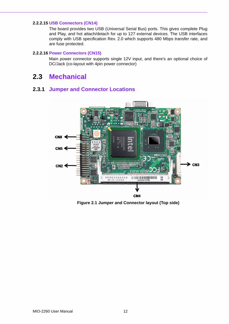
2.3.1 Jumper and Connector Locations
Figure 2.1 Jumper and Connector layout (Top side)
MIO-2260 User Manual 12

Chapter 2
H/W
Installation
Figure 2.2 Jumper and connector layout (Bottom side)
2.3.2 Board Dimensions
2.3.2.1 CPU Board Drawing
Figure 2.3 Board dimension layout (Top side)
13 MIO-2260 User Manual

Figure 2.4 Board dimension layout (Bottom side)
Figure 2.5 Board dimension layout (Coastline with power connector)
MIO-2260 User Manual 14
Chapter 2
H/W
Installation
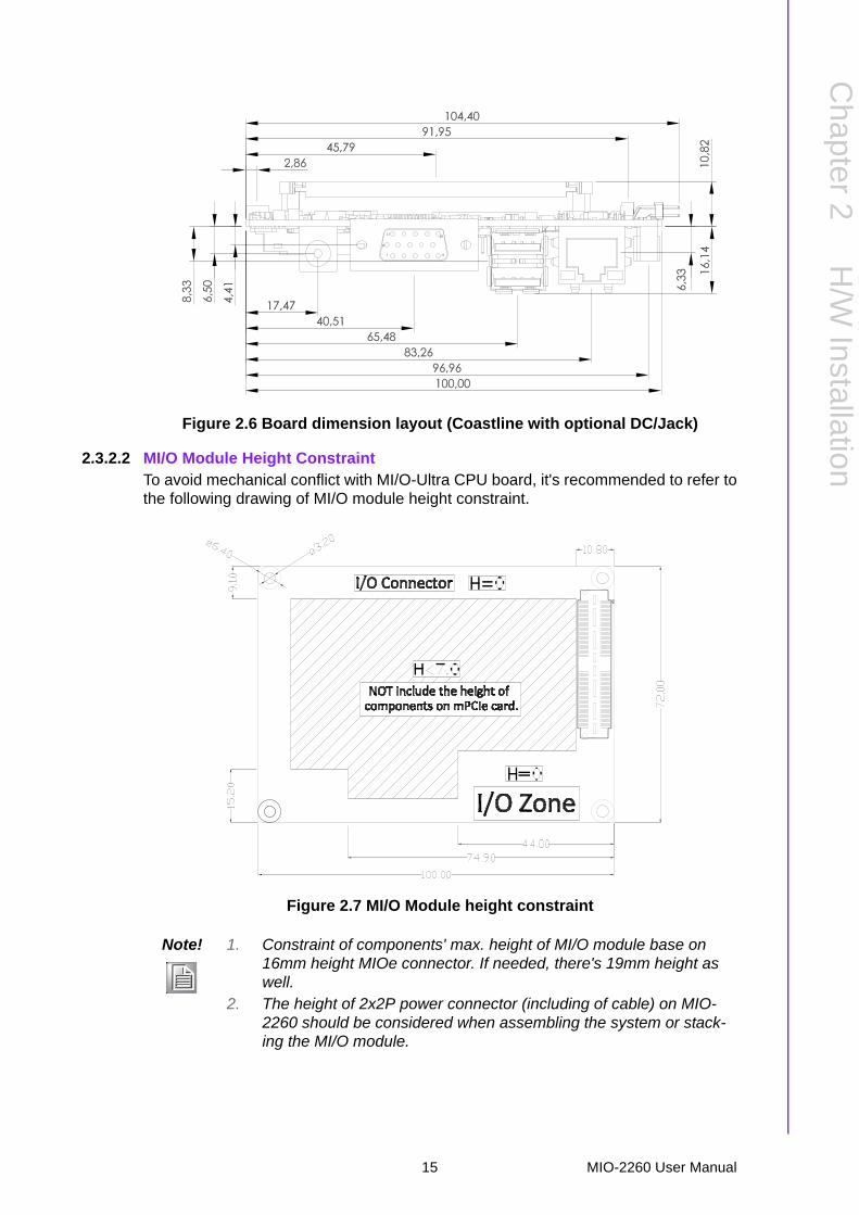
Figure 2.6 Board dimension layout (Coastline with optional DC/Jack)
2.3.2.2 MI/O Module Height ConstraintTo avoid mechanical conflict with MI/O-Ultra CPU board, it's recommended to refer tothe following drawing of MI/O module height constraint.
Figure 2.7 MI/O Module height constraint
Note! 1. Constraint of components' max. height of MI/O module base on 16mm height MIOe connector. If needed, there's 19mm height as well.
2. The height of 2x2P power connector (including of cable) on MIO-2260 should be considered when assembling the system or stack-ing the MI/O module.
15 MIO-2260 User Manual

2.3.2.3 Another Thermal Solution - Heat SpreaderMIO-2260 has an optional heat spreader to make whole system more compact.Using a heat spreader to conduct heat to your chassis can help a lot when system isextra compact or limited space for heat convection. Here are some guidelines forheat spreader:
1. For best heat conduction, the gap between chassis and heat spreader should be the smaller, the better.
2. The height of exsting heat spreader is 11.2mm (Advantech P/N: 1960053176T001). If you need some other height to fit chassis better, Advan-tech could custormize it for you. (Please contact our sales for details)
3. There are thermal grease and screws in heat spreader kit, thermal grease helps conduct better if chassis is quite close to heat spreader. Another suggestion is to use thermal pad if chassis isn't close enough to heat spreader. (The gap is suggested less than 3mm for better heat conduction and cost effective)
Figure 2.8 Illustration of heat spreader assembly
MIO-2260 User Manual 16

Chapter 3
3 BIOS settings
AMIBIOS has been integrated into many motherboards for over a decade. With theAMIBIOS Setup program, you can modify BIOS settings and control the various sys-tem features. This chapter describes the basic navigation of the PICO-2260 BIOSsetup screens.
Figure 3.1 Setup program initial screen
AMI's BIOS ROM has a built-in Setup program that allows users to modify the basicsystem configuration. This information is stored in battery-backed CMOS so it retainsthe Setup information when the power is turned off.
3.1 Entering Setup Turn on the computer and check for the -patch" code. If there is a number assignedto the patch code, it means that the BIOS supports your CPU. If there is no numberassigned to the patch code, please contact an Advantech application engineer toobtain an up-to-date patch code file. This will ensure that your CPU's system status isvalid. After ensuring that you have a number assigned to the patch code, press<DEL> and you will immediately be allowed to enter Setup.
MIO-2260 User Manual 18

Chapter 3
BIO
S settings
3.2 Main Setup When you first enter the BIOS Setup Utility, you will enter the Main setup screen. Youcan always return to the Main setup screen by selecting the Main tab. There are twoMain Setup options. They are described in this section. The Main BIOS Setup screenis shown below.
Figure 3.2 Main setup screen
The Main BIOS setup screen has two main frames. The left frame displays all theoptions that can be configured. Grayed-out options cannot be configured; options inblue can. The right frame displays the key legend.
Above the key legend is an area reserved for a text message. When an option isselected in the left frame, it is highlighted in white. Often a text message will accom-pany it.
3.2.1 System time / System date Use this option to change the system time and date. Highlight System Time or Sys-tem Date using the <Arrow> keys. Enter new values through the keyboard. Press the<Tab> key or the <Arrow> keys to move between fields. The date must be entered inMM/DD/YY format. The time must be entered in HH:MM:SS format.
19 MIO-2260 User Manual

3.3 Advanced BIOS Features Setup Select the Advanced tab from the PICO-2260 setup screen to enter the AdvancedBIOS Setup screen. You can select any of the items in the left frame of the screen,such as CPU Configuration, to go to the sub menu for that item. You can display anAdvanced BIOS Setup option by highlighting it using the <Arrow> keys. All AdvancedBIOS Setup options are described in this section. The Advanced BIOS Setupscreens is shown below. The sub menus are described on the following pages.
Figure 3.3 Advanced BIOS features setup screen
MIO-2260 User Manual 20
Chapter 3
BIO
S settings
3.3.1 CPU Configuration
Figure 3.4 CPU Configuration Setting
Max CPUID Value Limit
This item allows you to limit CPUID maximum value.
Execute-Disable Bit Capability
This item allows you to enable or disable the No-Execution page protection technol-ogy.
Hyper Threading Technology
This item allows you to enable or disable Intel? Hyper Threading technology.
Intel® C-STATE tech
This item allows the CPU to save more power under idle mode.
Enhanced C-States
CPU idle set to enhanced C-States, disabled by Intel? C-STATE tech item.
21 MIO-2260 User Manual

3.3.2 IDE Configuration
Figure 3.5 IDE Configuration
ATA/IDE Configuration
This item allows you to select Disabled / Compatible / Enhanced.
Legacy IDE Channels
When set to Enhanced mode you can select IDE or AHCI mode. When select Com-patible mode you can select SATA only / SATA pri, PATA sec or PATA only.
Primary/Secondary/Third IDE Master/Slave
BIOS auto detects the presence of IDE device, and displays the status of auto detec-tion of IDE device.
>Type: Select the type of SATA driver.[Not Installed][Auto][CD/DVD][ARMD]
>LBA/Large Mode: Enables or Disables the LBA mode.
>Block (Multi-Sector Transfer): Enables or disables data multi-sectors transfers.
>PIO Mode: Select the PIO mode.
>DMA Mode: Select the DMA mode.
>S.M.A.R.T.: Select the smart monitoring, analysis, and reporting technology.
>32Bit Data Transfer: Enables or disables 32-bit data transfer.
Hard Disk Write Protect
Disable/Enable device write protection. This will be effective only if device isaccessed through BIOS.
IDE Detect Time Out (Sec)
This item allows you to select the time out value for detecting ATA/ATAPI device(s).
MIO-2260 User Manual 22

Chapter 3
BIO
S settings
3.3.3 Super I/O Configuration
Figure 3.6 Super I/O Configuration
Serial Port1 / Port2 address
This item allows you to select serial port1 / port2 of base addresses.
Serial Port1 / Port2 IRQ
This item allows you to select serial port1 / port2 of IRQ.
WatchDog function
This item allows you to enable WatchDog function by minutes or seconds.
23 MIO-2260 User Manual

3.3.4 Hardware Health Configuration
Figure 3.7 Hardware health configuration
H/W Health Function
This item allows you to control H/W monitor of showing.
Temperature & Voltage show
CPU/System Temperature
Vcore / +3.3Vin / +5Vin / +12Vin / VBAT
MIO-2260 User Manual 24

Chapter 3
BIO
S settings
3.3.5 ACPI Settings
Figure 3.8 ACPI Settings
3.3.5.1 General ACPI Configuration
Figure 3.9 General ACPI Configuration
Suspend mode
Select the ACPI state used for system suspend.
Report Video on S3 Resume
This item allows you to invoke VA BIOS POST on S3/STR resume.
25 MIO-2260 User Manual

3.3.5.2 Advanced ACPI Configuration
Figure 3.10 Advanced ACPI Configuration
ACPI Version Features
This item allows you to enable RSDP pointers to 64-bit fixed system descriptiontables.
ACPI APIC support
Include APIC table pointer to RSDT pointer list.
AMI OEMB table
Include OEMB table pointer to R(x)SDT pointer lists.
Headless mode
Enable/Disable Headless operation mode through ACPI.
MIO-2260 User Manual 26

Chapter 3
BIO
S settings
3.3.5.3 Chipset ACPI Configuration
Figure 3.11 Chipset ACPI Configuration
Energy Lake Feature
Allows you to configure Intel's Energy Lake power management technology.
APIC ACPI SCI IRQ
Enable/Disable APIC ACPI SCI IRQ.
USB Device Wakeup From S3
Enable/Disable USB Device Wakeup from S3.
High Performance Event Timer
Enable/Disable High performance Event timer.
27 MIO-2260 User Manual

3.3.6 AHCI Configuration
Figure 3.12 Advanced ACPI Configuration
AHCI Ports0 / Port1
While entering setup, BIOS auto detects the presence of IDE devices. This displaysthe status of auto detection of IDE device.
3.3.7 APM Configuration
Figure 3.13 APM Configuration
MIO-2260 User Manual 28
Chapter 3
BIO
S settings
Power Management/APM
Enable or disable APM.
Power Button Mode
Power on, off, or enter suspend mode when the power button is pressed. The follow-ing options are also available.
Restore on AC power Loss
Use this to set up the system response after a power failure. The "Off" setting keepsthe system powered off after power failure, the "On" setting boots up the system afterfailure, and the "Last State" returns the system to the status just before power failure.
Resume On PME#
Enable / Disable PME to generate a wake event.
Resume On RTC Alarm
Enable / Disable RTC to generate a wake event.
3.3.8 Event Log Configuration
Figure 3.14 South Bridge ACPI Configuration
View Event Log
View all unread events on the event Log.
Mark all events as read
Mark all unread events as read.
Clear Event Log
Discard all events in the event Log.
29 MIO-2260 User Manual

3.3.9 MPS Configuration
Figure 3.15 MPS Configuration
MPS Revision
This item allows you to select MPS reversion.
3.3.10 Smbios Configuration
Figure 3.16 Smbios Configuration
Smbios Smi Support
SMBIOS SMI wrapper support for PnP function 50h-54h.
MIO-2260 User Manual 30

Chapter 3
BIO
S settings
3.3.11 USB Configuration
Figure 3.17 USB Configuration
Legacy USB Support
Enables support for legacy USB. Auto option disables legacy support if no USBdevices are connected.
USB 2.0 Controller Mode
This item allows you to select HiSpeed(480Mbps) or FullSpeed (12Mpbs).
BIOS EHCI Hand-Off
This is a workaround for OSes without EHCI hand-off support. The EHCI ownershipchange should claim by EHCI driver.
Hotplug USB FDD Support
A dummy FDD device is created that will be associated with the hotplugged FDDlater. Auto option creates this dummy device only if there is no USB FDD present.
31 MIO-2260 User Manual

>>> USB Mass Storage Device Configuration
Figure 3.18 USB Mass storage Device Configuration
USB Mass Storage Reset Delay
Number of sends POST wait for the USB mass storage device after start unit com-mand.
Emulation Type
If Auto, USB devices less than 530MB will be emulated as Floppy and remaining ashard drive. Force FDD option can be used to force a FDD formatted drive to boot asFDD(Ex. ZIP drive).
MIO-2260 User Manual 32

Chapter 3
BIO
S settings
3.4 Advanced PCI/PnP Settings Select the PCI/PnP tab from the PICO-2260 setup screen to enter the Plug and PlayBIOS Setup screen. You can display a Plug and Play BIOS Setup option by highlight-ing it using the <Arrow> keys. All Plug and Play BIOS Setup options are described inthis section. The Plug and Play BIOS Setup screen is shown below.
Figure 3.19 PCI/PNP Setup (top)
Clear NVRAM
Set this value to force the BIOS to clear the Non-Volatile Random Access Memory
(NVRAM).The Optimal and Fail-Safe default setting is No.
Plug & Play O/S
When set to No, BIOS configures all the device in the system. When set to Yes and ifyou install a Plug and Play operating system, the operating system configures thePlug and Play device not required for boot.
PCI Latency Timer
Value in units of PCI clocks for PCI device latency timer register.
Allocate IRQ to PCI VGA
When set to Yes will assigns IRQ to PCI VGA card if card requests IRQ. When set toNo will not assign IRQ to PCI VGA card even if card requests an IRQ.
Palette Snooping
This item is designed to solve problems caused by some non-standard VGA card.
PCI IDE BusMaster
When set to enabled BIOS uses PCI busmastering for reading/writing to IDE drives.
OffBoard PCI/ISA IDE Card
Some PCI IDE cards may require this to be set to the PCI slot number that is holdingthe card. When set to Auto will works for most PCI IDE cards.
33 MIO-2260 User Manual

IRQ3 / 4 / 5 / 7 / 9 / 10 /11
This item allows you respectively assign an interruptive type for IRQ-3, 4, 5, 7, 9, 10,11.
DMA Channel0 / 1 / 3 / 5 / 6 / 7
When set to Available will specified DMA is available to be used by PCI/PnP devices.When set to Reserved will specified DMA will Reserved for use by legacy ISAdevices.
Reserved Memory Size
This item allows you to reserved size of memory block for legacy ISA device.
3.5 Boot Settings
Figure 3.20 Boot Setup Utility
MIO-2260 User Manual 34

Chapter 3
BIO
S settings
3.5.1 Boot settings Configuration
Figure 3.21 Boot Setting Configuration
Quick Boot
This item allows BIOS to skip certain tests while booting. This will decrease the timeneeded to boot the system.
Quiet Boot
If this option is set to Disabled, the BIOS displays normal POST messages. IfEnabled, an OEM Logo is shown instead of POST messages.
AddOn ROM Display Mode
Set display mode for option ROM.
Bootup Num-Lock
Select the Power-on state for Numlock.
PS/2 Mouse Support
Select support for PS/2 Mouse.
Wait For "F1' If Error
Wait for the F1 key to be pressed if an error occurs.
Hit "DEL' Message Display
Displays -Press DEL to run Setup" in POST.
Interrupt 19 Capture
This item allows option ROMs to trap interrupt 19.
Bootsafe function
This item allows you to enables or disables bootsafe function.
35 MIO-2260 User Manual

3.6 Security Setup
Figure 3.22 Password Configuration
Select Security Setup from the PICO-2260 Setup main BIOS setup menu. All Secu-rity Setup options, such as password protection and virus protection are described inthis section. To access the sub menu for the following items, select the item andpress <Enter>:
Change Supervisor / User Password
Boot sector Virus protection: The boot sector virus protection will warn if any programtries to write to the boot sector.
MIO-2260 User Manual 36

Chapter 3
BIO
S settings
3.7 Advanced Chipset Settings
Figure 3.23 Advanced Chipset Settings
3.7.1 North Bridge Chipset Configuration
Figure 3.24 North Bridge Configuration
DRAM Frequency
This item allows you to manually changed DRAM frequency.
37 MIO-2260 User Manual

Configure DRAM Timing by SPD
This item allows you to enables or disables detect by DRAM SPD .
Initate Graphic Aadapter
This item allows you to select which graphics controller to use as the primary bootdevice.
Internal Graphics Mode Select
Select the amount of system memory used by the Internal graphics device.
Figure 3.25 Video function configuration
DVMT Mode Select
Displays the active system memory mode.
DVMT/FIXED Memory
Specify the amount of DVMT / FIXED system memory to allocate for video memory.
Boot Display Device
Select boot display device at post stage.
Flat Panel Type
This item allows you to select which panel resolution you wants.
Spread Spectrum Clock
This item allows you to enables or disables spread spectrum clock.
Backlight Control 1 Type
This item allows you to select backlight control type.
Backlight 1 Level
This item allows you to select backlight level.
MIO-2260 User Manual 38

Chapter 3
BIO
S settings
3.7.2 South Bridge Chipset Configuration
Figure 3.26 South Bridge Configuration
USB Functions
Enables or disables the USB function.
USB 2.0 Controller
Enables or disables the USB 2.0 controller.
Intel 82567V controller
Enables or disables the intel LAN controller.
Boot Rom
Enables or disables internal LAN boot.
Wake Up From S5
Enables or disables LAN1 wake up from S5 function.
HDA Controller
Enables or disables the HDA controller.
SMBUS Controller
Enables or disables the SMBUS controller.
SLP_S4# Min. Assertion Width
This item allows you to set a delay of sorts.
39 MIO-2260 User Manual

3.8 Exit Option
Figure 3.27 Exit Option
3.8.1 Save Changes and Exit When you have completed system configuration, select this option to save yourchanges, exit BIOS setup and reboot the computer so the new system configurationparameters can take effect.
1. Select Exit Saving Changes from the Exit menu and press <Enter>. The following message appears: Save Configuration Changes and Exit Now? [Ok] [Cancel]
2. Select Ok or cancel.
3.8.2 Discard Changes and Exit Select this option to quit Setup without making any permanent changes to the systemconfiguration.
1. Select Exit Discarding Changes from the Exit menu and press <Enter>. The following message appears: Discard Changes and Exit Setup Now? [Ok] [Cancel]
1. Select Ok to discard changes and exit. Discard Changes 2. Select Discard Changes from the Exit menu and press <Enter>.
3.8.3 Load Optimal Defaults The PICO-2260 automatically configures all setup items to optimal settings when youselect this option. Optimal Defaults are designed for maximum system performance,but may not work best for all computer applications. In particular, do not use the Opti-mal Defaults if your computer is experiencing system configuration problems. SelectLoad Optimal Defaults from the Exit menu and press <Enter>.
MIO-2260 User Manual 40

Chapter 3
BIO
S settings
3.8.4 Load Fail-Safe Defaults The PICO-2260 automatically configures all setup options to fail-safe settings whenyou select this option. Fail-Safe Defaults are designed for maximum system stability,but not maximum performance. Select Fail-Safe Defaults if your computer is experi-encing system configuration problems.
1. Select Load Fail-Safe Defaults from the Exit menu and press <Enter>. The following message appears: Load Fail-Safe Defaults? [OK] [Cancel]
2. Select OK to load Fail-Safe defaults.
41 MIO-2260 User Manual

MIO-2260 User Manual 42
Chapter 4
4 S/W Introduction & Installation
4.1 S/W Introduction The mission of Advantech Embedded Software Services is to "Enhance quality of lifewith Advantech platforms and Microsoft Windows embedded technology.” We enableWindows embedded software products on Advantech platforms to more effectivelysupport the embedded computing community. Customers are freed from the hassleof dealing with multiple vendors (Hardware suppliers, System integrators, EmbeddedOS distributor) for projects. Our goal is to make Windows embedded software solu-tions easily and widely available to the embedded computing community.
4.2 Driver Installation To install the drivers please just insert the CD into CD-ROM, select the drivers thatyou want to install, then run .exe (set up) file under each chipset folder and followDriver Setup instructions to complete the installation.
4.2.1 Windows XP ProfessionalTo install the drivers for Windows XP Professional, insert the CD into the CD-ROM, itwill auto-detect the hardware platform and then pop up with the "Embedded Comput-ing Install Wizard box”; just select the drivers that you want to install then click InstallAll Selected drivers. Follow the Driver Setup Wizard instructions; click "Next" to com-plete the installation.
4.2.2 Other OSTo install the drivers for another Windows OS or Linux, please browse the CD to runthe setup file under each chipset folder on the CD-ROM.
4.3 Value-Added Software ServicesSoftware API: An interface that defines the ways by which an application programmay request services from libraries and/or operating systems. Provides not only theunderlying drivers required but also a rich set of user-friendly, intelligent and inte-grated interfaces, which speeds development, enhances security and offers add-onvalue for Advantech platforms. It plays the role of catalyst between developer andsolution, and makes Advantech embedded platforms easier and simpler to adopt andoperate with customer applications.
4.3.1 SUSI IntroductionTo make hardware easier and convenient to access for programmers, Advantech hasreleased a suite of API (Application Programming Interface) in the form of a programlibrary. The program Library is called Secured and Unified Smart Interface or SUSIfor short.
In modern operating systems, user space applications cannot access hardwaredirectly. Drivers are required to access hardware. User space applications accesshardware through drivers. Different operating systems usually define different inter-face for drivers. This means that user space applications call different functions forhardware access in different operating systems. To provide a uniform interface foraccessing hardware, an abstraction layer is built on top of the drivers and SUSI issuch an abstraction layer. SUSI provides a uniform API for application programmersto access the hardware functions in different Operating Systems and on differentAdvantech hardware platforms.
MIO-2260 User Manual 44

Chapter 4
S/W
Introduction&
Installation
Application programmers can invoke the functions exported by SUSI instead of call-ing the drivers directly. The benefit of using SUSI is portability. The same set of API isdefined for different Advantech hardware platforms. Also, the same set of API isimplemented in different Operating Systems including Windows XP and WindowsCE. This user’s manual describes some sample programs and the API in SUSI. Thehardware functions currently supported by SUSI can be grouped into a few catego-
ries including Watchdog, I2C, SMBus, GPIO, and VGA control. Each category of APIin SUSI is briefly described below.
4.3.2 Software APIs
4.3.2.1 The GPIO APIGeneral Purpose Input/Output is a flexible parallel interface that allows a variety ofcustom connections. It allows users to monitor the level of signal input or set the out-put status to switch on/off a device. Our API also provides Programmable GPIO,which allows developers to dynamically set the GPIO input or output status.
4.3.2.2 The I2C API
I2C is a bi-directional two-wire bus that was developed by Phillips for use in their tele-visions in the 1980s and nowadays is used in various types of embedded systems.
The strict timing requirements defined in the I2C protocol has been taken care of bySUSI. Instead of asking application programmers to figure out the strict timing
requirements in the I2C protocol, the I2C API in SUSI can be used to control I2Cdevices by invoking other function calls. SUSI provides a consistent programminginterface for different Advantech boards. That means user programs using SUSI areportable among different Advantech boards as long as the boards and SUSI providethe required functionalities. Overall product development times can be greatlyreduced using SUSI.
4.3.2.3 The SMBus APIThe System Management Bus (SMBus) is a two-wire interface defined by Intel® Cor-
poration in 1995. It is based on the same principles of operation of I2C and is used inpersonal computers and servers for low-speed system management communica-tions. Nowadays, it can be seen in many types of embedded systems. As with otherAPI in SUSI, the SMBus API is available on many platforms including Windows XPand Windows CE.
4.3.2.4 The Display Control APIThere are two kinds of VGA control APIs, backlight on/off control and brightness con-trol. Backlight on/off control allows a developer to turn on or off the backlight, and tocontrol brightness smoothly.
1. Brightness Control– The Brightness Control API allows a developer to interface with an embed-
ded device to easily control brightness.2. Backlight Control
– The Backlight API allows a developer to control the backlight (screen) on/off in an embedded device.
45 MIO-2260 User Manual

4.3.2.5 The Watchdog APIA watchdog timer (abbreviated as WDT) is a hardware device which triggers anaction, e.g. rebooting the system, if the system does not reset the timer within a spe-cific period of time. The WDT API in SUSI provides developers with functions such asstarting the timer, resetting the timer, and setting the timeout value if the hardwarerequires customized timeout values.
4.3.2.6 The Hardware Monitor API The hardware monitor (abbreviated as HWM) is a system health supervision capabil-ity achieved by placing certain I/O chips along with sensors for inspecting the targetof interests for certain condition indexes, such as fan speed, temperature and voltageetc.
However, due to the inaccuracy among many commercially available hardware mon-itoring chips, Advantech has developed a unique scheme for hardware monitoring -achieved by using a dedicated micro-processor with algorithms specifically designedfor providing accurate, real-time and reliable data content; helping protect your sys-tem in a more reliable manner.
4.3.2.7 The Power Saving API1. CPU Speed
– Make use of Intel SpeedStep technology to reduce power consumption. The system will automatically adjust the CPU Speed depending on system load-ing.
2. System Throttling– Refers to a series of methods for reducing power consumption in computers
by lowering the clock frequency. APIs allow the user to lower the clock from 87.5% to 12.5%.
4.3.3 SUSI Utilities
4.3.3.1 BIOS FlashThe BIOS Flash utility allows customers to update the flash ROM BIOS version, oruse it to back up current BIOS by copying it from the flash chip to a file on custom-ers’disk. The BIOS Flash utility also provides a command line version and API for fastimplementation into customized applications.
4.3.3.2 Embedded Security IDThe embedded application is the most important property of a system integrator. Itcontains valuable intellectual property, design knowledge and innovation, but it iseasily copied! The Embedded Security ID utility provides reliable security functionsfor customers to secure their application data within embedded BIOS.
4.3.3.3 Monitoring utilityThe Monitoring utility allows the customer to monitor system health, including volt-age, CPU and system temperature and fan speed. These items are important to adevice; if critical errors happen and are not solved immediately, permanent damagemay be caused.
4.3.3.4 eSOS The eSOS is a small OS stored in BIOS ROM. It will boot up in case of a main OScrash. It will diagnose the hardware status, and then send an e-mail to a designatedadministrator. The eSOS also provides remote connection: Telnet server and FTPserver, allowing the administrator to rescue the system.
MIO-2260 User Manual 46
Chapter 4
S/W
Introduction&
Installation
4.3.3.5 Flash LockFlash Lock is a mechanism that binds the board and CF card (SQFlash) together.The user can “Lock” SQFlash via the Flash Lock function and “Unlock” it via BIOSwhile booting. A locked SQFlash cannot be read by any card reader or boot fromother platforms without a BIOS with the “Unlock” feature.
4.3.4 SUSI InstallationSUSI supports many different operating systems. Each subsection below describeshow to install SUSI and related software on a specific operating system. Please referto the subsection matching your operating system.
4.3.4.1 Windows XPIn windows XP, you can install the library, drivers and demo programs onto the plat-form easily using the installation tool--The SUSI Library Installer. After the installerhas executed, the SUSI Library and related files for Windows XP can be found in thetarget installation directory. The files are listed in the following table.
The following section illustrates the installation process.
1. Extract Susi.zip.2. Double-click the "Setup.exe" file.The installer searches for a previous installation of the SUSI Library. If it locates one,a dialog box opens asking whether you want to modify, repair or remove the soft-ware. If a previous version is located, please see the [Maintenance Setup] section. Ifit is not located, an alternative window appears. Click Next.
Directory Contents
\Library Susi.libLibrary for developing the applications on Windows XP.
Susi.dllDynamic library for SUSI on Windows XP.
\Demo SusiDemo.EXEDemo program on Windows XP.
Susi.dllDynamic library for SUSI on Windows XP.
\Demo\SRC Source code of the demo program on Windows XP.
Note! The SUSI Library Installer screen shots shown below are examples only. Your screens may vary depending on your particular version.
47 MIO-2260 User Manual

4.3.4.2 Windows CEIn windows CE, there are three ways to install the SUSI Library, you can install itmanually or use Advantech CE-Builder to install the library or just copy the programsand the library onto a compact flash card.
Express Installation:
You can use Advantech CE-Builder to load the library into the image.
First, you click the My Component tab. In this tab, you click Add New Category button to add a new category, e.g. the
SUSI Library. Then you can add a new file in this category, and upload the SUSI.dll for this
category. After these steps, you can select the SUSI Library category you created for
every project.
Manual Installation:
You can add the SUSI Library into the image by editing any bib file.
First you open project.bib in the platform builder.
Add this line to the MODULES section of project.bibSusi.dll $(_FLATRELEASEDIR)\Susi.dll NK SH
If you want to run the window-based demo, add following line:SusiTest.exe $(_FLATRELEASEDIR)\SusiTest.exe
If you want to run the console-based demo, add following lines:Watchdog.exe $(_FLATRELEASEDIR)\Watchdog.exe NK S GPIO.exe $(_FLATRELEASEDIR)\GPIO.exe NK S SMBUS.exe $(_FLATRELEASEDIR)\SMBUS.exe NK S
Place the three files into any files directory. Build your new Windows CE operating system.
4.3.5 SUSI Sample ProgramsSample Programs
The sample programs demonstrate how to incorporate SUSI into your program.There are sample programs for two categories of operating system, i.e. Windows XPand Windows CE. The sample programs run in graphics mode in Windows XP andWindows CE. The sample programs are described in the subsections below.
Windows Graphics Mode
There are sample programs of Windows in graphics mode for two categories of oper-ating system, i.e. Windows CE and Windows XP. Each demo application contains anexecutable file SusiDemo.exe, a shared library Susi.dll and source code within therelease package. The files of Windows CE and Windows XP are not compatible witheach other.
SusiDemo.exe is an executable file and it requires the shared library, Susi.dll, todemonstrate the SUSI functions. The source code of SusiDemo.exe also has twoversions, i.e. Windows CE and Windows XP, and must be compiled under MicrosoftVisual C++ 6.0 on Windows XP or under Microsoft Embedded Visual C++ 4.0 onWindows CE. Developers must add the header file Susi.h and library Susi.lib to theirown projects when they want to develop something with SUSI.
MIO-2260 User Manual 48
Chapter 4
S/W
Introduction&
Installation
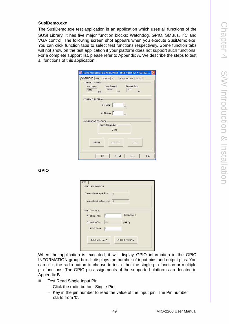
SusiDemo.exe
The SusiDemo.exe test application is an application which uses all functions of the
SUSI Library. It has five major function blocks: Watchdog, GPIO, SMBus, I2C andVGA control. The following screen shot appears when you execute SusiDemo.exe.You can click function tabs to select test functions respectively. Some function tabswill not show on the test application if your platform does not support such functions.For a complete support list, please refer to Appendix A. We describe the steps to testall functions of this application.
GPIO
When the application is executed, it will display GPIO information in the GPIOINFORMATION group box. It displays the number of input pins and output pins. Youcan click the radio button to choose to test either the single pin function or multiplepin functions. The GPIO pin assignments of the supported platforms are located inAppendix B.
Test Read Single Input Pin– Click the radio button- Single-Pin.– Key in the pin number to read the value of the input pin. The Pin number
starts from '0'.
49 MIO-2260 User Manual
– Click the READ GPIO DATA button and the status of the GPIO pin will be dis-played in (R/W) Result field.
Test Read Multiple Input Pin– Click the radio button- Multiple-Pins.– Key in the pin number from ‘0x01’ to ‘0x0F’ to read the value of the input pin.
The pin numbers are ordered bitwise, i.e. bit 0 stands for GPIO 0, bit 1 stands for GPIO 1, etc. For example, if you want to read pin 0, 1, and 3, the pin num-bers should be ‘0x0B’.
– Click READ GPIO DATA button and the statuses of the GPIO pins will be dis-played in (R/W) Result field.
Test Write Single Output Pin– Click the radio button- Single-Pin.– Key in the pin numbers you want to write. Pin numbers start from '0'.– Key in the value either '0' or '1' in (R/W) Result field to write the output pin you
chose above step.– Click the WRITE GPIO DATA button to write the GPIO output pin.
Test Write Multiple Output Pins– Click the radio button- Multiple-Pins.– Key in the pin number from ‘0x01’ to ‘0x0F’ to choose the multiple pin num-
bers to write the value of the output pin. The pin numbers are ordered bit-wise, i.e. bit 0 stands for GPIO 0, bit 1 stands for GPIO 1, etc. For example, if you want to write pin 0, 1, and 3, the pin numbers should be ‘0x0B’.
– Key in the value in (R/W) Result field from ‘0x01’ to ‘0x0F’ to write the value of the output pin. The pin numbers are ordered bitwise, i.e. bit 0 stands for GPIO 0, bit 1 stands for GPIO 1, etc. For example, if you want to set pin 0 and 1 high, 3 to low, the pin number should be ‘0x0B/, and then you should key in the value ‘0x0A’ to write.
– Click the WRITE GPIO DATA button to write the GPIO output pins.
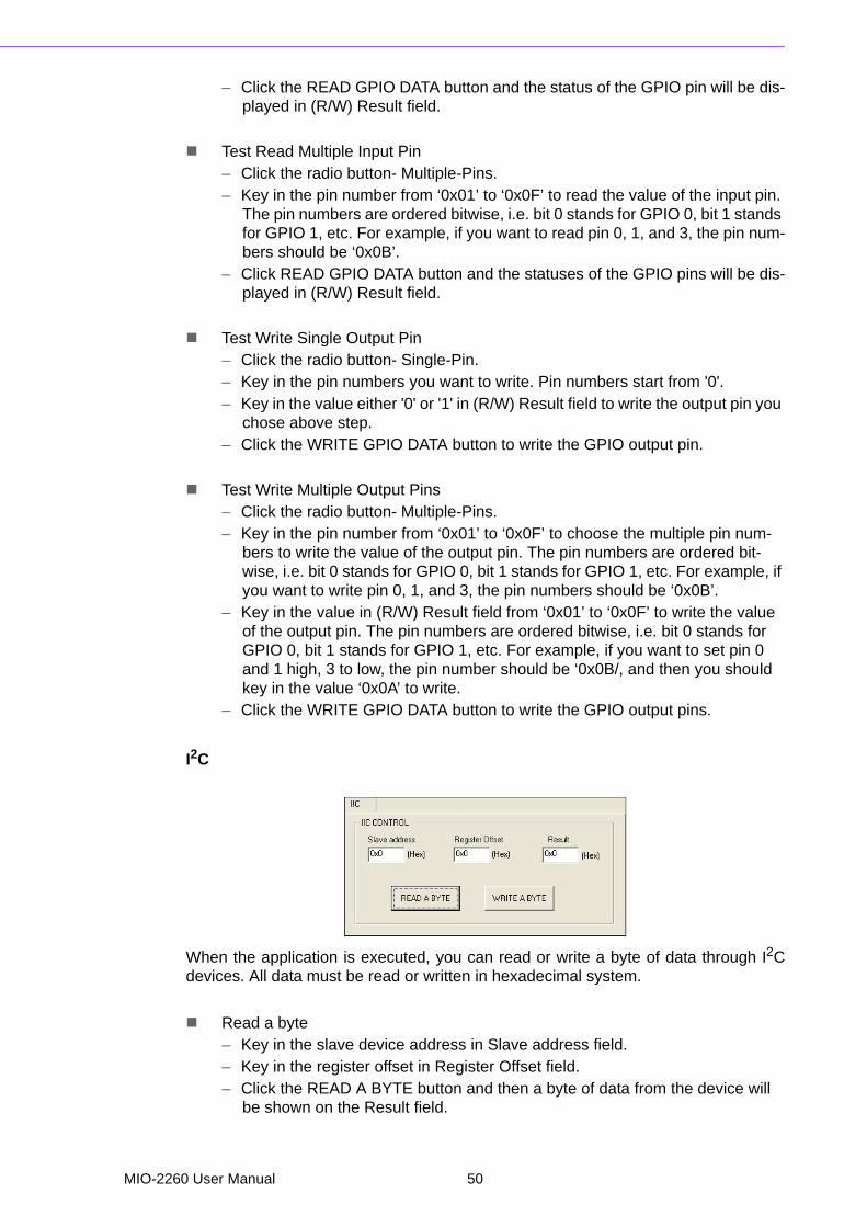
I2C
When the application is executed, you can read or write a byte of data through I2Cdevices. All data must be read or written in hexadecimal system.
Read a byte– Key in the slave device address in Slave address field.– Key in the register offset in Register Offset field.– Click the READ A BYTE button and then a byte of data from the device will
be shown on the Result field.
MIO-2260 User Manual 50

Chapter 4
S/W
Introduction&
Installation
Write a byte– Key in the slave device address in Slave address field.– Key in the register offset in Register Offset field.– Key in the desirous of data in Result field to write to the device.– Click the WRITE A BYTE button and then the data will be written to the
device through I2C.SMBus
When the application has executed, you can click the radio button to choose to testeach access mode, i.e. Access a byte, Access multiple bytes and Access a word. Alldata must be read or written in hexadecimal except the numbers for radio button:Access multiple bytes mode must be written in decimal. You can test the functional-ities of the watchdog as follows:
Read a byte– Click the radio button- Access a byte.– Key in the slave device address in the Slave address field.– Key in the register offset in the Register Offset field.– Click the READ SMBus DATA button and a byte of data from the device will
be shown on the Result field.
Write a byte– Click the radio button- Access a byte.– Key in the slave device address in Slave address field.– Key in the register offset in Register Offset field.– Key the desired data in the Result field to write to the device.– Click the WRITE SMBus DATA button and then the data will be written to the
device through SMBus.
Read a word– Click the radio button- Access a word.– Key in the slave device address in the Slave address field.– Key in the register offset in the Register Offset field.– Click the READ SMBus DATA button and then a word of data from the device
will be shown on the Result field.
51 MIO-2260 User Manual

Write a word– Click the radio button- Access a word.– Key in the slave device address in the Slave address field.– Key in the register offset in the Register Offset field.– Key in the desired data, such as 0x1234, in the Result field to write to the
device.– Click the WRITE SMBus DATA button and the data will be written to the
device through the SMBus. Read Multiple bytes
– Click the radio button- Access multiple bytes.– Key in the slave device address in the Slave address field.– Key in the register offset in the Register Offset field.– Key in the desired number of bytes, such as 3, in the right side field of radio
button- Access multiple bytes. The number must be written in decimal.– Click the READ SMBus DATA button and then all data from the device will be
divided from each other by commas and be shown in the Result field. Write Multiple bytes
– Click the radio button- Access multiple bytes.– Key in the slave device address in the Slave address field.– Key in the register offset in the Register Offset field.– Key in the desired number of bytes, such as 3, in the right side field of the
radio button- Access multiple bytes. The number must be written in decimal.– Key in all the desired data in the Result field in hexadecimal format, divided
by commas, for example, 0x50,0x60,0x7A.– Click the WRITE SMBus DATA button and all of the data will be written to the
device through the SMBus.
Display Control
When the application is executed, it will display two blocks of VGA control functions.The application can turn on or turn off the screen shot freely, and it also can tune thebrightness of the panels if your platform is being supported. You can test the function-alities of VGA control as follows:
MIO-2260 User Manual 52

Chapter 4
S/W
Introduction&
Installation
Screen on/off control– Click the radio button ON or push the key F11 to turn on the panel screen.– Click the radio button OFF or push the key F12 to turn off the panel screen.– The display chip of your platform must be in the support list in Appendix A, or
this function cannot work. Brightness control
– Move the slider in increments, using either the mouse or the direction keys, or click the UP button to increase the brightness.
– Move the slider in decrements, using either the mouse or the direction keys, or click the DOWN button to decrease the brightness.
Watchdog
When the application is executed, it will display watchdog information in the WATCH-DOG INFORMATION group box. It displays max timeout, min timeout, and timeoutsteps in milliseconds. For example, a 1~255 seconds watchdog will have 255000max timeout, 1000 min timeout, and 1000 timeout steps. You can test the functional-ity of the watchdog as follows:
Set the timeout value 3000 (3 sec.) in the SET TIMEOUT field and set the delay value 2000 (2 sec.) in the SET DELAY field, then click the START button. The Timeout Countdown field will countdown the watchdog timer and display 5000 (5 sec.).
Before the timer counts down to zero, you can reset the timer by clicking the REFRESH button. After you click this button, the Timeout Countdown field will display the value of the SET TIMEOUT field.
If you want to stop the watchdog timer, just click the STOP button.
53 MIO-2260 User Manual

Hardware Monitor
When the Monitor application is executed by clicking the button, hardware monitoringdata values will be displayed. If certain data values are not supported by the platform,the correspondent data field will be grayed-out with a value of 0.
For more details on MIO-2260 software API, please contact your dealer or AdvantechAE. API user manuals are also included on this CD.
MIO-2260 User Manual 54

Appendix A
A PIN Assignments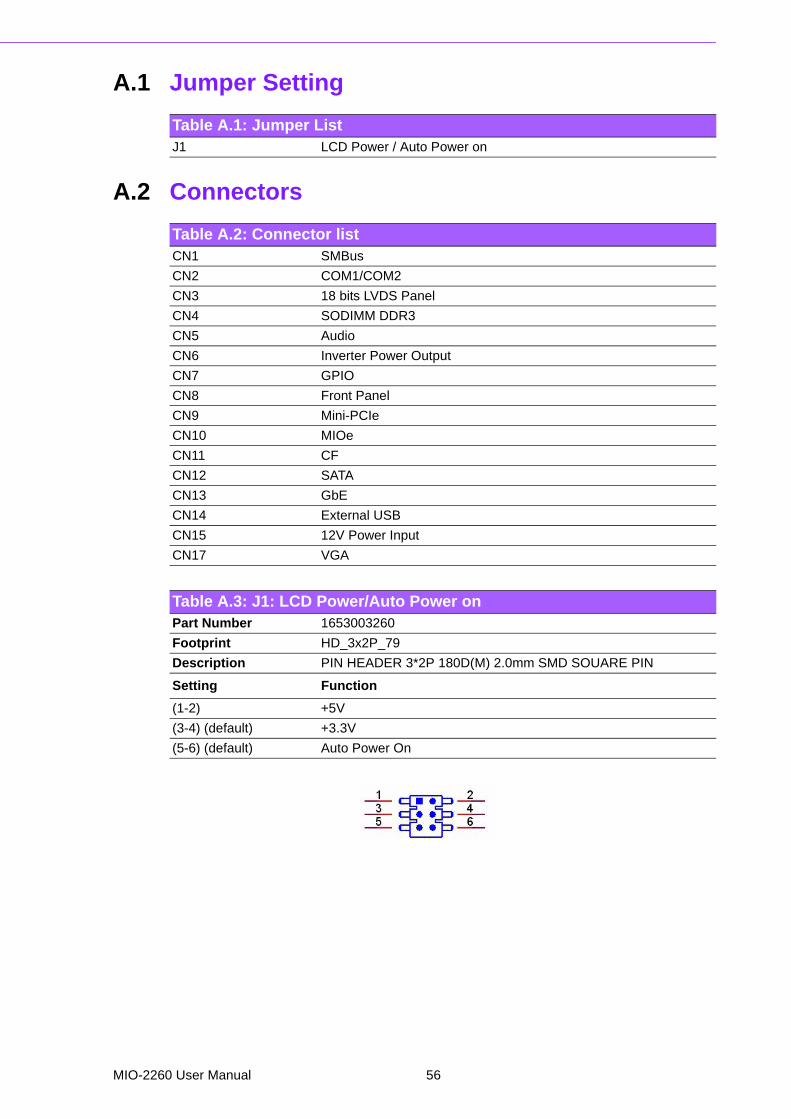
A.1 Jumper Setting
A.2 Connectors
Table A.1: Jumper ListJ1 LCD Power / Auto Power on
Table A.2: Connector listCN1 SMBus
CN2 COM1/COM2
CN3 18 bits LVDS Panel
CN4 SODIMM DDR3
CN5 Audio
CN6 Inverter Power Output
CN7 GPIO
CN8 Front Panel
CN9 Mini-PCIe
CN10 MIOe
CN11 CF
CN12 SATA
CN13 GbE
CN14 External USB
CN15 12V Power Input
CN17 VGA
Table A.3: J1: LCD Power/Auto Power onPart Number 1653003260
Footprint HD_3x2P_79
Description PIN HEADER 3*2P 180D(M) 2.0mm SMD SOUARE PIN
Setting Function
(1-2) +5V
(3-4) (default) +3.3V
(5-6) (default) Auto Power On
MIO-2260 User Manual 56

Appendix A
PIN
Assignm
ents
Table A.4: CN1: SMBusPart Number 1654904503
Footprint WF_4P_49_BOX_RA
Description CONN. SMD 4*1P 90D(M)1.25mm 85204-0400 0
Pin Pin Name
1 GND
2 SMB_DAT
3 SMB_CLK
4 +5V
Table A.5: CN2: COM1/COM2Part Number 1653003720
Footprint HD_10x2P_79_RA
Description PIN HEADER 10x2P 2.00mm 90D(M) SMD 21N22050-20J1
Pin Pin Name
1 DCD1#
2 DSR1#
3 RXD1
4 RTS1#
5 TXD1
6 CTS1#
7 DTR1#
8 RI1#
9 GND
10 GND
11 DCD2#
12 DSR2#
13 RXD2
14 RTS2#
15 TXD2
16 CTS2#
17 DTR2#
18 RI2#
19 GND
20 GND
57 MIO-2260 User Manual

HomeMatching Cable: 1700001795
Table A.6: CN3: 18 bits LVDS PanelPart Number 1655000753
Footprint WHL14HS-125-85204
Description
Pin Pin Name
1 +5V or +3.3V
2 +5V or +3.3V
3 LVDS0_D0+
4 LVDS0_D0-
5 LVDS0_D1+
6 LVDS0_D1-
7 LVDS0_D2+
8 LVDS0_D2-
11 LVDS0_CLK+
12 LVDS0_CLK-
13 GND
14 GND
Table A.7: CN4: SODIMMDDR3_204Part Number 1651001814
Footprint SODIMMDDR3_204P_AS0A626-N2
Description
Pin Pin Name
MIO-2260 User Manual 58
Appendix A
PIN
Assignm
ents
Table A.8: CN5: AudioPart Number 1653003719
Footprint HD_5x2P_79_RA_21N22050
Description PIN HEADER 5x2P 2.00mm 90D(M) SMD 21N22050
Pin Pin Name
1 LOUTR
2 LINR
3 GND
4 GND
5 LOUTL
6 LINL
7 GND
8 GND
9 NC
10 NC
Table A.9: CN6: Inverter Power OutputPart Number 1655905100
Footprint WF_5P_49_BOX_RA
Description Wafer 1.25mm 5P 90D Male SMD 852040
Pin Pin Name
1 +12V
2 GND
3 ENABKL
4 VBR
5 +5V
59 MIO-2260 User Manual
Table A.10: CN7: GPIOPart Number 1653005261
Footprint HD_5x2P_79
Description PIN HEADER 5x2P 2.0mm 180D(M) SMD 21N22050
Pin Pin Name
1 +5V
2 GPIO4
3 GPIO0
4 GPIO5
5 GPIO1
6 GPIO6
7 GPIO2
8 GPIO7
9 GPIO3
10 GND
Table A.11: CN8: Front PanelPart Number 1653004883
Footprint HD_3x2_79_RA
Description PIN HEADER 2x3P 2.00mm 90D(M) SMD
Pin Pin Name
1 Power Button Pin1
2 Power LED+
3 Power Button Pin2 ,Reset Button Pin2, Power LED-
4 HDD LED+
5 Reset Button Pin1
6 HDD LED-
MIO-2260 User Manual 60

Appendix A
PIN
Assignm
ents
Table A.12: CN9: Mini PCIEPart Number 00A00000660
Footprint MINIPCIE_HALF_PICO2600
Description
Pin Pin Name
1 WAKE#
2 +3.3VSB
3 NC
4 GND
5 NC
6 +1.5V
7 NC
8 NC
9 GND
10 NC
11 REFCLK-
12 NC
13 REFCLK+
14 NC
15 GND
16 NC
17 NC
18 GND
19 NC
20 NC
21 GND
22 PERST#
23 PERn0
24 +3.3VSB
25 PERp0
26 GND
27 GND
28 +1.5V
29 GND
30 SMB_CLK
31 PETn0
32 SMB_DAT
33 PETp0
34 GND
35 GND
36 USB D-
37 GND
38 USB D+
39 +3.3VSB
40 GND
41 +3.3VSB
42 NC
61 MIO-2260 User Manual

43 GND
44 NC
45 NC
46 NC
47 NC
48 +1.5V
49 NC
50 GND
51 NC
52 +3.3VSB
53 NC
54 NC
55 GND
56 GND
Table A.13: CN10: MIO 3.0 Part Number 1654006235
Footprint BB_40x2P_32_1625x285_2HOLD
Description
Pin Pin Name
1 GND
2 GND
3 PCIE_RX0+
4 PCIE_TX0+
5 PCIE_RX0-
6 PCIE_TX0-
7 GND
8 GND
9 PCIE_RX1+
10 PCIE_TX1+
11 PCIE_RX1-
12 PCIE_TX1-
13 GND
14 GND
15 PCIE_RX2+
16 PCIE_TX2+
17 PCIE_RX2-
18 PCIE_TX2-
19 GND
20 GND
21 PCIE_RX3+
22 PCIE_TX3+
23 PCIE_RX3-
24 PCIE_TX3-
25 GND
26 GND
Table A.12: CN9: Mini PCIE
MIO-2260 User Manual 62
Appendix A
PIN
Assignm
ents
27 PCIE_CLK+
28 LOUTL
29 PCIE_CLK-
30 LOUTR
31 GND
32 AGND
33 SMB_CLK
34 NC
35 SMB_DAT
36 NC
37 NC
38 NC
39 RESET#
40 NC
41 SLP_S3#
42 CLK33M
43 SLP_S5#
44 LPC_AD0
45 NC
46 LPC_AD1
47 NC
48 LPC_AD2
49 NC
50 LPC_AD3
51 NC
52 LPC_DRQ#0
53 NC
54 LPC_SERIRQ
55 NC
56 LPC_FRAME#
57 NC
58 GND
59 NC
60 USB0_D+
61 NC
62 USB0_D-
63 NC
64 GND
65 NC
66 USB1_D+/USB_SSTX+
67 NC
68 USB1_D-/USB_SSTX-
69 NC
70 GND
71 NC
72 USB2_D+/USB_SSRX+
73 NC
Table A.13: CN10: MIO 3.0
63 MIO-2260 User Manual

74 USB2_D-/USB_SSRX-
75 NC
76 GND
77 NC
78 USB_OC#
79 +12VSB
80 NC
83 GND
84 GND
85 GND
86 GND
87 +5VSB
88 +5VSB
89 +5VSB
90 +5VSB
Table A.13: CN10: MIO 3.0
MIO-2260 User Manual 64
Appendix A
PIN
Assignm
ents
Table A.14: CN11: CFPart Number 1653025211
Footprint CF_50P_N7E50-7516PK-20
Description HEADER 50P 90D(M) ANGLE Standard SMT for Compack
Pin Pin Name
1 GND
2 D03
3 D04
4 D05
5 D06
6 D07
7 CS0#
8 GND
9 GND
10 GND
11 GND
12 GND
13 +5V
14 GND
15 GND
16 GND
17 GND
18 A02
19 A01
20 A00
21 D00
22 D01
23 D02
24 NC
25 CD2#
26 CD1#
27 D11
28 D12
29 D13
30 D14
31 D15
32 CS1#
33 VS1#
34 IORD#
35 IOWR#
36 WE#
37 IREQ
38 +5V
39 CSEL#
40 VS2#
41 RESET
42 IORDY
65 MIO-2260 User Manual

43 INPACK#
44 REG#
45 DASP#
46 PDIAG#
47 D08
48 D09
49 D10
50 GND
Table A.15: CN12: SATAPart Number 1654007578
Footprint SATA_7P_WATF-07DBN6SB1U
Description Serial ATA 7P 1.27mm 180D(M) SMD WATF-07DBN6SB1U
Pin Pin Name
1 GND
2 TX+
3 TX-
4 GND
5 RX-
6 RX+
7 GND
Table A.14: CN11: CF
MIO-2260 User Manual 66

Appendix A
PIN
Assignm
ents
Table A.16: CN13: LANPart Number 1652004356
Footprint RJ45_14P_RT7-194AAM1A
Description
Pin Pin Name
1 BI_DA+(GHz)
2 BI_DA-(GHz)
3 BI_DB+(GHz)
4 BI_DC+(GHz)
5 BI_DC-(GHz)
6 BI_DB-(GHz)
7 BI_DD+(GHz)
8 BI_DD-(GHz)
H3 GND
H4 GND
Table A.17: CN14: External USBPart Number 1654009513
Footprint USB_8P_UB1112C-8FDE-4F
Description
Pin Pin Name
1 +5V
2 D-
3 D+
4 GND
67 MIO-2260 User Manual

Table A.18: CN15: 12V Power InputPart Number 1655404090
Footprint ATXCON-2X2-42
Description ATX PWR CONN. 2x2P 4.2mm 180D(M) DIP 24W4310-04S
Pin Pin Name
1 GND
2 GND
3 +12V
4 +12V
Table A.19: CN17: VGAPart Number 1654000055
Footprint DBVGA-VF5MS
Description D-SUB Conn. 15P 90D(F) DIP 070242FR015S200ZU
Pin Pin Name
1 RED
2 GREEN
3 BLUE
4 NC
5 GND
6 GND
7 GND
8 GND
9 NC
10 GND
11 NC
12 DDAT
13 HSYNC
14 VSYNC
15 DCLK
MIO-2260 User Manual 68

Appendix B
B WDT & GPIO
B.1 Watchdog Timer Sample Code1. Watchdog function:
;The SCH3114 Runtime base I/O address is A00h
;Setting WatchDog time value location at offset 66h
;If set value "0", it is mean disable WatchDog function.
Superio_GPIO_Port = A00h
mov dx,Superio_GPIO_Port + 66h
mov al,00h
out dx,al
.model small
.486p
.stack 256
.data
SCH3114_IO EQU A00h
.code
org 100h
.STARTup
;====================================================
;47H
;enable WDT function bit [0]=0Ch
;====================================================
mov dx,SCH3114_IO + 47h
mov al,0Ch
out dx,al
;====================================================
;65H
;bit [1:0]=Reserved
;bit [6:2]Reserve=00000
;bit [7] WDT time-out Value Units Select
;Minutes=0 (default) Seconds=1
;====================================================
mov dx,SCH3114_IO + 65h ;
mov al,080h
out dx,al
;====================================================
;66H
;WDT timer time-out value
;bit[7:0]=0~255
;====================================================
mov dx,SCH3114_IO + 66h
mov al,01h
out dx,al
;====================================================
;bit[0] status bit R/W
;WD timeout occurred =1
MIO-2260 User Manual 70

Appendix B
WD
T &
GP
IO
;WD timer counting = 0
;====================================================
mov dx,SCH3114_IO + 68h
mov al,01h
out dx,al
.exit
END
2. GPIO Sample Code
1. GPIO function:
The SCH3114 Runtime base I/O address is A00h
.model small
.486p
.stack 256
.data
SCH3114_IO EQU A00h
.code
org 100h
.STARTup
;====================================================
;GIPO 0~GPIO 7 Function define(SCH3114_IO Port offset + 23h / 24h / 25h / 26h /27h / 29h / 2Ah / 2Bh)
; bit [0] = In/Out: = 1 Input, = 0 output
; bit [1] = Polarity : 1 Invert, = 0 No Invert
; bit [7] = Output Type Select : 1 = Open Drian, 0 = Push Pull
;====================================================
mov dx,SCH3114_IO + 23h ;GPIO 0
mov al,00h ;program GPIO 0 as output
out dx,al
;====================================================
;GIPO 0~GPIO 7 DATA Register (SCH3114_IO Port offset + 4Bh)
; bit [0] = GPIO 0 High/Low: = 1 High, = 0 Low
; bit [1] = GPIO 1 High/Low: = 1 High, = 0 Low
; bit [2] = GPIO 2 High/Low: = 1 High, = 0 Low
; bit [3] = GPIO 3 High/Low: = 1 High, = 0 Low
; bit [4] = GPIO 4 High/Low: = 1 High, = 0 Low
; bit [5] = GPIO 5 High/Low: = 1 High, = 0 Low
; bit [6] = GPIO 6 High/Low: = 1 High, = 0 Low
; bit [7] = GPIO 7 High/Low: = 1 High, = 0 Low
;====================================================
mov dx,SCH3114_IO + 4Bh ;
mov al,01h ;Set GPIO 0 as High level
out dx,al
.exit
71 MIO-2260 User Manual

MIO-2260 User Manual 72

Appendix C
C System Assignments
C.1 System I/O Ports
C.2 1st MB Memory Map
C.3 DMA Channel Assignments
Table C.1: System I/O Ports
Addr. Range (Hex) Device
000-01F DMA Controller
20h-2Dh Interrupt Controller
50h-52h Timer/Counter
060-06F 8042 (keyboard controller)
070-07F Real-time clock, non-maskable interrupt (NMI)
mask
080-09F DMA page register
0A0-0BF 0A0-0BF
0C0-0DF DMA controller
170h-177h IDE Controller
1F0h-1F7h IDE Controller
2F8-2FF Serial port 2
3F8-3FF Serial port 1
Table C.2: 1st MB memory map
Addr. Range (Hex) Device
F0000h - FFFFFh System ROM
D0000h - EFFFFh Unused (reserved for Ethernet ROM)
C0000h - CE7FFh Expansion ROM (for VGA BIOS)
B8000h - BFFFFh CGA/EGA/VGA text
B0000h - B7FFFh Unused
A0000h - AFFFFh EGA/VGA graphics
00000h - 9FFFFh Base memory
Table C.3: DMA channel assignments
Channel Function
0 Available
1 Reserved (audio)
2 Floppy disk (8-bit transfer)
3 Available (parallel port)
4 Cascade for DMA controller 1
5 Available
6 Available
7 Available
* Audio DMA select 1, 3, or 5** Parallel port DMA select 1 (LPT2) or 3 (LPT1)
MIO-2260 User Manual 74

Appendix C
System
Assignm
ents
C.4 Interrupt Assignments
Table C.4: Interrupt assignments
Interrupt# Interrupt source
IRQ0 Interval timer
IRQ1 Keyboard
IRQ2 Interrupt from controller 2 (cascade)
IRQ3 COM2
IRQ4 COM1
IRQ5 Reserved
IRQ6 Reserved
IRQ7 Reserved
IRQ8 RTC
IRQ9 Reserved
IRQ10 Reserved
IRQ11 Reserved
IRQ12 PS/2 mouse
IRQ13 Math Coprocessor
IRQ14 Primary IDE
IRQ15 Secondary IDE
75 MIO-2260 User Manual

www.advantech.comPlease verify specifications before quoting. This guide is intended for referencepurposes only.All product specifications are subject to change without notice.No part of this publication may be reproduced in any form or by any means,electronic, photocopying, recording or otherwise, without prior written permis-sion of the publisher.All brand and product names are trademarks or registered trademarks of theirrespective companies.© Advantech Co., Ltd. 2011