user manual for hmx1-as2
TRANSCRIPT

User Manual for HMX1-AS2

Disclaimer. The information in this document is provided in connection with Gleichmann Electronics Research
(GE Research) products. GE Research makes no representations or warranties with respect to the accuracy or
completeness of the document and reserves the right to make changes to specification and product description at
any time without notice. GE Research does not accept any liability to the accuracy of the design completed by
the developer, whether original design, copied from schematics and/or application notes, supplied by GE Research
and/or otherwise. The final circuit integrity and testing is solely the responsibility of the design authority. GE
Research accept no responsibility and/or liability.
HMX1-AS2 manual
Martina ZeinzingerVersion: 2008-04-04
Copyright Notice
This document is copyrighted, 2008, by Gleichmann Electronics Research (Austria) GmbH & Co KG. All rights are
reserved. Gleichmann Electronics Research (Austria) GmbH & Co KG reserves the right to make improvements to the
products described in this manual at any time without notice. No part of this manual may be reproduced, copied,
translated or transmitted in any form or by any means without the prior written permission of Gleichmann Electronics
Research (Austria) GmbH & Co KG. Information provided in this manual is intended to be accurate and reliable.
However, Gleichmann Electronics Research (Austria) GmbH & Co KG assumes no responsibility for its use, nor for any
infringements upon the rights of third parties which may result from its use.
2

CONTENTS
Contents
Contents 3
1 Introduction 71.1 System Overview . . . . . . . . . . . . . . . . . . . . . . . . . . . . . . . . . . . . 7
2 General Information 92.1 Reset . . . . . . . . . . . . . . . . . . . . . . . . . . . . . . . . . . . . . . . . . . . 92.2 LEDs . . . . . . . . . . . . . . . . . . . . . . . . . . . . . . . . . . . . . . . . . . 92.3 AES . . . . . . . . . . . . . . . . . . . . . . . . . . . . . . . . . . . . . . . . . . . 9
3 Clock Factory 113.1 Clock Distribution . . . . . . . . . . . . . . . . . . . . . . . . . . . . . . . . . . . 113.2 Configuration via Flash . . . . . . . . . . . . . . . . . . . . . . . . . . . . . . . . 113.3 Fan Control . . . . . . . . . . . . . . . . . . . . . . . . . . . . . . . . . . . . . . . 12
4 CPLD for USB Blaster and FCP 134.1 FCP . . . . . . . . . . . . . . . . . . . . . . . . . . . . . . . . . . . . . . . . . . . 134.2 JTAG configuration . . . . . . . . . . . . . . . . . . . . . . . . . . . . . . . . . . 134.3 Connection to the CPLD for Clock Factory and Configuration . . . . . . . . . . . 14
5 Elastomer Connectors 155.1 Module Connectors . . . . . . . . . . . . . . . . . . . . . . . . . . . . . . . . . . . 15
5.1.1 JTAG . . . . . . . . . . . . . . . . . . . . . . . . . . . . . . . . . . . . . . 155.1.2 Global Reset . . . . . . . . . . . . . . . . . . . . . . . . . . . . . . . . . . 155.1.3 Clocks . . . . . . . . . . . . . . . . . . . . . . . . . . . . . . . . . . . . . . 155.1.4 Power Control . . . . . . . . . . . . . . . . . . . . . . . . . . . . . . . . . 155.1.5 I/Os for Peripherals . . . . . . . . . . . . . . . . . . . . . . . . . . . . . . 15
5.2 Hpe Childboard Connectors . . . . . . . . . . . . . . . . . . . . . . . . . . . . . . 165.2.1 Hpe Childboard 1 . . . . . . . . . . . . . . . . . . . . . . . . . . . . . . . 165.2.2 Hpe Childboard 2 . . . . . . . . . . . . . . . . . . . . . . . . . . . . . . . 17
6 Power Supply 216.1 Power Source . . . . . . . . . . . . . . . . . . . . . . . . . . . . . . . . . . . . . . 216.2 Generated Power . . . . . . . . . . . . . . . . . . . . . . . . . . . . . . . . . . . . 216.3 I/O Power . . . . . . . . . . . . . . . . . . . . . . . . . . . . . . . . . . . . . . . . 21
7 DUT-FPGA 237.1 PLLs . . . . . . . . . . . . . . . . . . . . . . . . . . . . . . . . . . . . . . . . . . . 237.2 Connection to the CPLD for Clock Factory and Configuration . . . . . . . . . . . 23
7.2.1 Configuration Pins for the DUT-FPGA#1 by the CPLD for Clock Factoryand Configuration . . . . . . . . . . . . . . . . . . . . . . . . . . . . . . . 23
7.2.2 Clocks . . . . . . . . . . . . . . . . . . . . . . . . . . . . . . . . . . . . . . 247.2.3 I/O Pins: Negative Clock Inputs . . . . . . . . . . . . . . . . . . . . . . . 24
3

CONTENTS
7.2.4 Fast PLL Clock Inputs . . . . . . . . . . . . . . . . . . . . . . . . . . . . . 247.2.5 PLL Output Clocks . . . . . . . . . . . . . . . . . . . . . . . . . . . . . . 257.2.6 Other I/O pins . . . . . . . . . . . . . . . . . . . . . . . . . . . . . . . . . 25
7.3 Connection to the CPLD for USB Blaster and FCP . . . . . . . . . . . . . . . . . 257.4 Dedicated Pins on the DUT-FPGA#1 . . . . . . . . . . . . . . . . . . . . . . . . 26
7.4.1 Thermal Control . . . . . . . . . . . . . . . . . . . . . . . . . . . . . . . . 267.4.2 JTAG Pins . . . . . . . . . . . . . . . . . . . . . . . . . . . . . . . . . . . 267.4.3 Configuration Pins . . . . . . . . . . . . . . . . . . . . . . . . . . . . . . . 267.4.4 Other dedicated Configuration Pins . . . . . . . . . . . . . . . . . . . . . 27
7.5 JTAG Pins for internal JTAG Core . . . . . . . . . . . . . . . . . . . . . . . . . . 277.6 Clock from Oscillator . . . . . . . . . . . . . . . . . . . . . . . . . . . . . . . . . . 287.7 Hpe Childboard 1 . . . . . . . . . . . . . . . . . . . . . . . . . . . . . . . . . . . 28
7.7.1 Differential Receive Channels . . . . . . . . . . . . . . . . . . . . . . . . . 287.7.2 Transmit Channels . . . . . . . . . . . . . . . . . . . . . . . . . . . . . . . 297.7.3 Configuration Pins for the DUT-FPGA#1 by the Hpe Childboard 1 . . . 307.7.4 Other pins . . . . . . . . . . . . . . . . . . . . . . . . . . . . . . . . . . . 30
7.8 Hpe Childboard 2 . . . . . . . . . . . . . . . . . . . . . . . . . . . . . . . . . . . 317.9 Connector to the Mainboard . . . . . . . . . . . . . . . . . . . . . . . . . . . . . 33
7.9.1 Hpe Childboard 3 . . . . . . . . . . . . . . . . . . . . . . . . . . . . . . . 337.9.2 Hpe Childboard 4 . . . . . . . . . . . . . . . . . . . . . . . . . . . . . . . 367.9.3 Audio Interface (AC97) . . . . . . . . . . . . . . . . . . . . . . . . . . . . 387.9.4 A/D Converter (ADC) and D/A Converter (DAC) . . . . . . . . . . . . . 387.9.5 CAN Interface . . . . . . . . . . . . . . . . . . . . . . . . . . . . . . . . . 387.9.6 External User Interface . . . . . . . . . . . . . . . . . . . . . . . . . . . . 397.9.7 Ethernet Interface . . . . . . . . . . . . . . . . . . . . . . . . . . . . . . . 397.9.8 Expansion Connector . . . . . . . . . . . . . . . . . . . . . . . . . . . . . 407.9.9 Parallel Flash . . . . . . . . . . . . . . . . . . . . . . . . . . . . . . . . . . 407.9.10 Human Interface . . . . . . . . . . . . . . . . . . . . . . . . . . . . . . . . 407.9.11 I2C . . . . . . . . . . . . . . . . . . . . . . . . . . . . . . . . . . . . . . . . 417.9.12 LCD Connector . . . . . . . . . . . . . . . . . . . . . . . . . . . . . . . . . 417.9.13 LIN Interface . . . . . . . . . . . . . . . . . . . . . . . . . . . . . . . . . . 417.9.14 Memory . . . . . . . . . . . . . . . . . . . . . . . . . . . . . . . . . . . . . 417.9.15 PS/2 Ports . . . . . . . . . . . . . . . . . . . . . . . . . . . . . . . . . . . 437.9.16 Serial Interface (RS232) . . . . . . . . . . . . . . . . . . . . . . . . . . . . 437.9.17 SD Card Reader . . . . . . . . . . . . . . . . . . . . . . . . . . . . . . . . 437.9.18 Asynchronous SRAM . . . . . . . . . . . . . . . . . . . . . . . . . . . . . 447.9.19 3 x 4 Key Matrix . . . . . . . . . . . . . . . . . . . . . . . . . . . . . . . . 447.9.20 USB Target Connector . . . . . . . . . . . . . . . . . . . . . . . . . . . . . 447.9.21 USB Host and On The Go (OTG) Connector . . . . . . . . . . . . . . . . 457.9.22 VGA Interface . . . . . . . . . . . . . . . . . . . . . . . . . . . . . . . . . 467.9.23 System Reset . . . . . . . . . . . . . . . . . . . . . . . . . . . . . . . . . . 477.9.24 Powerl Reset . . . . . . . . . . . . . . . . . . . . . . . . . . . . . . . . . . 48
8 Specifications 49
8.1 HMX1-AS2 Board . . . . . . . . . . . . . . . . . . . . . . . . . . . . . . . . . . . 498.1.1 HMX1-AS2 in the case . . . . . . . . . . . . . . . . . . . . . . . . . . . . . 49
4

CONTENTS
9 Trouble Shooting 519.1 Testing the hardware . . . . . . . . . . . . . . . . . . . . . . . . . . . . . . . . . . 51
9.1.1 Generell Information . . . . . . . . . . . . . . . . . . . . . . . . . . . . . . 519.1.2 Software which is recommended for testing . . . . . . . . . . . . . . . . . 519.1.3 Testroutine started automatically . . . . . . . . . . . . . . . . . . . . . . . 519.1.4 Starting the testroutine over Ethernet . . . . . . . . . . . . . . . . . . . . 53
Index 56
5

CONTENTS
6

1 Introduction
AttentionThe HMX1-AS2 is a FPGA development system therefore it is not designed for a worst casescenario. If it is used with very high performance, it is possible that the FGPA is not cooledsufficiently and/or the case overheats. It is the user’s responsibility to proof the feasibility of theFPGA-design. In case of overheating, the clocks comming from the Clock Factory switchs off.If this protection mechanism is evaded, the consequence is the expiration of any guarantee.
The name HMX1-AS2 stands for Hpe Module X1 stuffed with an Altera Stratix II FPGA.HMX1-AS2-60 means that the FPGA EP2S60F1020C3N is stuffed,HMX1-AS2-90 means that the FPGA EP2S90F1020C3N is stuffed andHMX1-AS2-180 means that the FPGA EP2S180F1020C3N is stuffed.
The HMX1-AS2 is designed to be used in conjunction with the mainboard Hpe midi. Themodule is compatible to the former FPGA modules from Gleichmann Electronics Reseach, how-ever, the mechanical outlines are different. A Altera Stratix II device is the main part of thismodule which can be used for the functional verification of high complex digital circuits and forSEmulation. The connection to the mainboard is done by two elastomer module connectors.
1.1 System Overview
The following features are the most important parts of this FPGA module:
• one 1020 pin Altera Stratix II FPGA EP2S60F1020C3N, EP2S90F1020C3N or EP2S180F1020C3N(DUT-FPGA#1)
• two 364 pin elastomer module connectors (X1, X2)
• two 132 pin elastomer Hpe childboard connectors (X3, X4), one with low voltage differen-tial signals (LVDS)
• flash for the configuration of the FPGA
• CPLD for clock distribution (clock factory), configuration and fan control
• CPLD for FPGA Code Protection (FCP) and Altera USB blaster
The FPGA on the HMX1-AS2 is the fastest one of its family and it is used in a 1020-pinpackage. Beside that, it is possible to choose between three differnt sizes of the FPGA. TheEP2S180F1020C3N offers three times the size of the EP2S60F1020C3N.
The naming convention of this manual is based on the assumption that the HMX1-AS2 isused together with the Hpe midi and the Hpe childboard HC-PCIe in the SEmulator mode.The HC-PCIe has to be stucked on the Hpe childboard connector X3 and mainly consits of ofan FPGA—the Communication Controller—which handles the connection to the PC via PCIExpress. Figure 1.1 gives you a graphical overview of the components on the HMX1-AS2.
7

1 Introduction
Figure 1.1: The HMX1-AS2 Block Diagram
8

2 General Information
2.1 Reset
There is one system wide reset (PWR RESET#) which resets all CPLDs and the FPGA on theHMX1-AS2.
2.2 LEDs
Looking at the front side of your HMX1-AS2 you find nine LEDs. If the HMX1-AS2 is in thecase together with a mainboard, you find the LEDs on the front side in the upper row (refer tofigure 2.1).
The first two LEDs from the right side are yellow and in a box named Fan. The right LEDshows the activity of of the fan for the Communication Controller on the HC-PCIe. The LEDon the left shows the fan activity for the DUT-FPGA#1.
The next two LEDs are green and in a box named Power. The right one shows power goodfor 2.5 V and the left one signals power good for 1.2 V.
The next three LEDs are in a box named ComCon and have a blue colour. These LEDs canonly be lit when the HC-PCIe is connected. The left one stands for data transfer (DT), the onein the middle signals connection to the PC via PCI Express (PC) and the left one shows thatthe Communication Controller is ready (CC).
The two blue LEDs on the left side are named Config Done. The right one shows that theClock Factory (CF) is prepared and the left one signals that the DUT-FPGA#1 is configured.
2.3 AES
AES is a block cipher standard. The DUT-FPGA#1 can be protected with AES. The key forAES can only be programmed once to each FPGA. That is to say, when the key is programmed,it can be neither changed nor deleted any more. Each configuration for this protected FPGA hasto be encrypted with the key before it is configured to the FPGA. In the FPGA the bit streamis decrypted with the same key during configuration.
If you with to use the AES, please contact Gleichmann Electronics Research, because thegeneration and programming of the key has to be done in our factory.
Due to the fact that with this methode, it is not possible to use the FPGA without encryptionany more, there is an alternative technology realised on the HMX1-AS2: The FCP. For moreinformation refer to section 4.1.
9

2 General Information
Figure 2.1: The front side of the SEmulator Engine
10

3 Clock Factory
3.1 Clock Distribution
The mainboard delivers three clocks (two from a socket and one from extern) to the CPLD forClock Factory and Configuration. Moreover, two PLL outputs from the FPGA are connected tothe CPLD for Clock Factory and Configuration. The clocks can be distributed to most of theclock pins of the DUT-FPGA#1 (refer to figure 3.1). The rules how the clocks are distributedare made by the user. He/She is provided a GUI with the Hpe desk, where the connectioncan be determined. After this step the CPLD for Clock Factory and Configuration has to bereconfigured.
A red line in the figure indicates a differential signal pair. For more information how theCPLD for Clock Factory and Configuration is connnected to the DUT-FPGA#1 refer to section7.2. In section 7.2.2 you find the clock input pins which are connected from the CPLD for ClockFactory and Configuration to the DUT-FPGA#1 and in section 7.2.5 pins for the clock outputconnection from the DUT-FPGA#1 to the CPLD for Clock Factory and Configuration can beseen. Concerning the clock output from the DUT-FPGA#1: although the CPLD for ClockFactory and Configuration can not handle differential clocks, it is possible to use both signals(the positive and the negative one) as independent single ended connection.
Because it is possible for the user to determine the clock distribution, it is necessary thatthe CPLD for Clock Factory and Configuration is reconfigured each time this distribution haschanged. This is done by the Hpe desk via the JTAG chain (Altera USB blaster) or via theCommunication Controller on the HC-PCIe.
3.2 Configuration via Flash
It is possible to configure the DUT-FPGA#1 by the CPLD for Clock Factory and Configuration.The configuration data is stored in the flash as a *.pof file. The flash disposes of common flashinterface (CFI). The Altera MAXII parallel flash loader (PFL) feature in the CPLD for ClockFactory and Configuration provides an easy way to program the flash memory device throughthe JTAG interface, and the logic to control configuration from the flash memory device to theDUT. The FPGA is configured immediately after power up.
For generating the *.pof file for the flash the some steps have to be taken in the Quartus®
software. First choose File – Convert Programming Files. . . and make the following settings:
• Programming file type: Programmer Object File (.pof)
• Configuration devilce: CFI 64MB
• Mode: Fast Passive Parallel
• File name: choose a name for the output file in this box
• check Memory Map File
• Options. . . set Start address (32-bit hexadecimal): 0x600000
• select SOF Data in the Input files to convert window
• click to Add File. . . and choose your *.sof file
11

3 Clock Factory
Clk0Clk1Clk2Clk3Clk4Clk5Clk6Clk7Clk8Clk9Clk10Clk11Clk12Clk13
Clk15Clk14
DUT#1
AC
97_B
ITC
LK
US
BD
_C
LK
OU
T
ET
H_T
XC
LK
ET
H_R
XC
LK
CB
3_C
LK
PS
2_M
CL
KP
S2_K
BD
AT
HMX1−AS2
ClockFactory
Hpe_midi
100MHz
CL
K0
CL
K1
CL
K_E
XT
62.5MHz
ChildBoard 2
PLL5_OUT0PLL5_OUT1PLL5_FB/OUT2
CB2_CLK2CB2_CLK0CB2_CLK1
CB1_RX_CLK1CB1_CLK
ChildBoard 1
PLL12_OUT0PLL12_OUT1PLL12_FB/OUT2
AC
97_E
XT
_C
LK
CB
4_C
LK
PLL11_OUT0PLL11_OUT1PLL11_FB/OUT2
PLL6_OUT0PLL6_OUT1PLL6_FB/OUT2
Figure 3.1: The Clock Distribution on the HMX1-AS2 .
• click to Generate
After having generated your *.pof file, you can open the Programmer in the Quartus® soft-ware. Provided that the usb cable is connected to the HMX1-AS2 and to your PC chooseUSB-Blaster [USB-x] (x stands for a number) with the button Hardware Setup. . . . After click-ing to Auto Detect you should see two devices: a EPM1270 and the FPGA. The EPM1270 isthe CPLD for Clock Factory and Configuration and contains the flash CFI 64MB. For this flashchoose the generated *.pof file, check the Program/Configure box and click to Start. Conse-quently, the flash is programmed and the FPGA is configured with the design after switching offand on the power.
Due to the fact that the needed configuration signals of the DUT-FPGA#1 are connected tothe CPLD for Clock Factory and Configuration, it is possible for the user to configure the FPGAwith this system. This is helpful when the HMX1-AS2 is used as FPGA development platform.The flash is big enough (64 Mbit) to hold the configuration files for one EP2S180. For moreinformation refer to the Altera documentation.
If the SEmulator is used, it is not possible to configure the FPGA by using the flash becausethe signals are engaged by the SEmulator which configures the FPGA.
3.3 Fan Control
On top of the FPGA a fan is fixed. The needed voltage (12 V) has to be provided via an extraconnector (X7) from the mainboard. The output of the temperature diode of the FPGA is con-nected to the CPLD for Clock Factory and Configuration via a temperature sensor. The CPLDfor Clock Factory and Configuration controlles the fan via pulse width modulation (PWM). Ifthe CPLD for Clock Factory and Configuration is not configured, the fan runs at full speed.
12

4 CPLD for USB Blaster and FCP
4.1 FCP
The FCP protects the IP core (e.g. the SEmulator) within the DUT-FPGA#1. In order to beable to use the advantages of FCP, a black box with the FPGA part of the FCP design has tobe ordered. Ask Gleichmann Electronics Research for usage.
When using the FCP it is necessary to to switch power off and on and then reconfigure theDUT. That is to say, if the current design is working with the FCP, and FCP should run afterreconfiguration as well, switch off the power to your boards, then switch it on again and startwith the reconfiguration. If you start to reconfigure the DUTs immediately (without turning offand on the power), the FCP won’t work (for security reasons).
4.2 JTAG configuration
The CPLD for USB Blaster and FCP also contains the configuration for using the Altera USBblaster. That is to say that only a simple USB cable is necessary to configure the chips on theHMX1-AS2 via JTAG.
There are two possible ways to use JTAG. The first one is via the Altera USB blaster (onconnector X5) and the other way is via the HC-PCIe. For using the Altera USB blaster only asimple USB cable is required because the Altera USB blaster is on board on the HMX1-AS2.
By default, the JTAG chain consists of two devices:
1. the CPLD for Clock Factory and Configuration and
2. the DUT-FPGA#1.
By default is is not possible to use the Altera USB blaster if the HC-PCIe is stucked on theHMX1-AS2 and connected to the PC (signaled via a high on CB1 PC CON and the blue LEDPC in the middle of the box named ComCon). In this case the JTAG chain can only be reachedvia PCI Express and the Communication Controller.
Moreover, it is possible to design an own JTAG core in customer design (which is in DUT-FPGA#1) and put it into the JTAG chain. Therefore the HC-PCIe is needed. If the signalCB1 SEL DUT JTAG is driven low by the Communication Controller, the JTAG chain consistsof three devices:
1. the CPLD for Clock Factory and Configuration,
2. the DUT-FPGA#1 and
3. the internal JTAG design of DUT-FPGA#1.
By a resistor jumper—stuff R0627 and R0628 instead of R0630 with 0 ohm resistors—it ispossible to loop the JTAG chain to the mainboard. This is advantageous if there is a device onthe mainboard that should be in the chain as well. By now, the JTAG chain looks like this:
1. the CPLD for Clock Factory and Configuration,
2. the chips on the mainboard,
3. the DUT-FPGA#1 and
4. optional an internal JTAG design of DUT-FPGA#1.
13

4 CPLD for USB Blaster and FCP
4.3 Connection to the CPLD for Clock Factory and Configuration
A bus of 41 bits connects the CPLD for USB Blaster and FCP with the CPLD for Clock Factoryand Configuration. This bus is reserved for internal use.
14

5 Elastomer Connectors
5.1 Module Connectors
The HMX1-AS2 is connected to the mainboard via the elastomer module connectors (X1 andX2). Below you find a brief summary of the most important pins. For more detailed informationrefer to the manual of the Hpe midi.
5.1.1 JTAG
Five signals are reserved for JTAG configuration:
• Test Data Input (TDI)
• Test Data Output (TDO)
• Test ClocK (TCK)
• Test Mode Select Input (TMS)
• Test ReSeT (TRST)
By default there is no JTAG connection available between the HMX1-AS2 and the mainboardbecause usually there is no configurable chip on the mainboard. However, if it is necessary, thereis a possibility to expand the JTAG chain to the mainboard. By a resistor jumper—stuff R0627and R0628 instead of R0630 with 0 ohm resistors—it is possible to loop the JTAG chain to themainboard. Now one or more devices on the mainboard are in the chain as well. The JTAGchain is made up by the chips on the HMX1-AS2 (CPLD for Clock Factory and Configurationand DUT-FPGA#1) and by the chips on the mainboard.
5.1.2 Global Reset
There is one system wide reset (PWR RESET#) which resets all CPLDs and the FPGA on theHMX1-AS2.
5.1.3 Clocks
Three clocks (two from a socket and one from extern) are delivered from the mainboard via theconnectors to the CPLD for Clock Factory and Configuration.
5.1.4 Power Control
5 V and 3.3 V are delivered via the two elastomer module connectors. Additionally, three signalsare reserved for power control. This feature is not used at the moment.
5.1.5 I/Os for Peripherals
In sum there are 473 I/O signals available between the DUT-FPGA#1 and the connectors. TheHMX1-AS2 is compatible with the mainboard Hpe midi. However, the signals CB3 DATA[88]to CB3 DATA[96] are only available when the EP2S90F1020C3N or the EP2S180F1020C3N isused. If the EP2S60F1020C3N is populated, then these signals are not connected on the FPGA.
15

5 Elastomer Connectors
5.2 Hpe Childboard Connectors
The HMX1-AS2 is featured with two Hpe childboard connectors. The Hpe childboard is used toadd additional hardware or interfaces to the HMX1-AS2. The Hpe childboard 1 on connector X3can handle LVDS signals and can be used for the HC-PCIe in order to be able to use the SEm-ulator engine. This Hpe childboard connector can also be used for most other Hpe childboards.However, not all pins are connected to the DUT-FPGA#1. Refer to section 5.2.1 for moredetails.
The Hpe childboard 2 on connector can be used for all Hpe childboard but the HC-PCIe.
5.2.1 Hpe Childboard 1
This Hpe childboard can be used for LVDS signals and is especially prepared for the SEmulator.
This connector (X3) has the purpose to handle nearly all Hpe childboards which work withup to 85 I/O pins. Beside that, it has the feature of 16 LVDS receiver pairs and 16 LVDStransmiter pairs. By default, all I/O signals work with a power supply of 2.5 V. However, thisI/O voltage can be changed to 3.3 V by setting the signal CB1 SEL LVDS VAL to low. Thissignal is controlled by the Hpe childboard. As usual 3.3 V are delivered to the Hpe childboardvia the connector. Additionally, 2.5 V are delivered to the Hpe childboard as well.
In table 5.1 and 5.2 you find the pin connection for this Hpe childboard. The signal namesare for a Hpe childboard with Communication Controller and PCI Express (HC-PCIe). Never-theless, most of the signals can be used as regular I/Os as well and only the emphasised ones donot have a connection to the an I/O pin on the DUT-FPGA#1.
The emphasised signals have the following meaning:
• CB1 SEL LVDS VAL: Pulled to low (or left floating) causes 2.5 V I/O supply on thesignals pins of the DUT-FPGA#1 which are connected to the Hpe childboard 1. Drivenhigh causes 3.3 V I/O supply voltage on these pins.
• CB1 CONF DONE: Needed for configuring the DUT-FPGA#1.
• CB1 STATUS#: Needed for configuring the DUT-FPGA#1.
• CB1 DCLK: Needed for configuring the DUT-FPGA#1.
• CB1 CONFIG#: Needed for configuring the DUT-FPGA#1.
• CB1 SEL DUT JTAG: If this pin is driven low, it is possible to put an own JTAG coreinto the JTAG chain.
• CB1 CC READY: Connected to a LED, signals that the Communication Controller isprepared.
• CB1 DATA: Connected to a LED, signals that the Communication Controller is trans-miting/receiving data.
• CB1 PC CON: Connected to a LED, signals that the Communication Controller is con-nected to the PC via PCI Express.
• CB1 FAN: Connected to a LED, signals that fan for the Communication Controller isactivated.
• CB1 TDO: JTAG pin (test data out), needed for the configuration of Clock Factory andDUT-FPGA#1 via Hpe childboard.
16

5.2 Hpe Childboard Connectors
Odd Side A Even Side APin Number Signal Name Pin Number Signal Name
A1 CB1 RX CLK1+ A2 CB1 TX CLK1+A3 CB1 RX CLK1- A4 CB1 TX CLK1-A5 CB1 RX 01+ A6 CB1 TX 01+A7 CB1 RX 01- A8 CB1 TX 01-A9 CB1 RX 02+ A10 CB1 TX 02+A11 CB1 RX 02- A12 CB1 TX 02-A13 CB1 RX 03+ A14 CB1 TX 03+A15 CB1 RX 03- A16 CB1 TX 03-A17 CB1 RX CLK2+ A18 CB1 TX CLK2+A19 CB1 RX CLK2- A20 CB1 TX CLK2-A21 CB1 RX 04+ A22 CB1 TX 04+A23 CB1 RX 04- A24 CB1 TX 04-A25 CB1 RX 05+ A26 CB1 TX 05+A27 CB1 RX 05- A28 CB1 TX 05-A29 CB1 RX 06+ A30 CB1 TX 06+A31 CB1 RX 06- A32 CB1 TX 06-A33 VCC3V3 A34 GNDA35 VCC3V3 A36 GNDA37 VCC3V3 A38 GNDA39 VCC3V3 A40 GNDA41 VCC3V3 A42 GNDA43 VCC3V3 A44 GNDA45 VCC3V3 A46 GNDA47 VCC3V3 A48 GNDA49 CB1 CLK+ A50 CB1 CLK-A51 GND A52 GNDA53 CB1 DATA0 A54 CB1 DATA7A55 CB1 DATA1 A56 CB1 CONF DONEA57 CB1 DATA2 A58 CB1 STATUS#A59 CB1 DATA3 A60 CB1 DCLKA61 CB1 DATA4 A62 CB1 CONFIG#A63 CB1 DATA5 A64 CB1 CC READYA65 CB1 DATA6 A66 CB1 SEL DUT JTAG
Table 5.1: Pin connection for Hpe childboard 1, side A
• CB1 TDI: JTAG pin (test data in), needed for the configuration of Clock Factory andDUT-FPGA#1 via Hpe childboard.
• CB1 TMS: JTAG pin (test mode select), needed for the configuration of Clock Factoryand DUT-FPGA#1 via Hpe childboard.
• CB1 TCK: JTAG pin (test clock), needed for the configuration of Clock Factory andDUT-FPGA#1 via Hpe childboard.
5.2.2 Hpe Childboard 2
This connector (X4) has the purpose to handle nearly all Hpe childboards which work with upto 99 I/O pins. As usual 3.3 V are delivered to the Hpe childboard via the connector. Whenevera power supply higher than 1.5 V and lower than 3.3 V on the VCCVAR1 pins is available, apower multiplexer switches the VCCVAR1 to the VCCIO pins on the DUT-FPGA#1 that need
17

5 Elastomer Connectors
Odd Side B Even Side BPin Number Signal Name Pin Number Signal Name
B1 CB1 RX CLK3+ B2 CB1 TX CLK3+B3 CB1 RX CLK3- B4 CB1 TX CLK3-B5 CB1 RX 07+ B6 CB1 TX 07+B7 CB1 RX 07- B8 CB1 TX 07-B9 CB1 RX 08+ B10 CB1 TX 08+B11 CB1 RX 08- B12 CB1 TX 08-B13 CB1 RX 09+ B14 CB1 TX 09+B15 CB1 RX 09- B16 CB1 TX 09-B17 CB1 RX CLK4+ B18 CB1 TX CLK4+B19 CB1 RX CLK4- B20 CB1 TX CLK4-B21 CB1 RX 10+ B22 CB1 TX 10+B23 CB1 RX 10- B24 CB1 TX 10-B25 CB1 RX 11+ B26 CB1 TX 11+B27 CB1 RX 11- B28 CB1 TX 11-B29 CB1 RX 12+ B30 CB1 TX 12+B31 CB1 RX 12- B32 CB1 TX 12-B33 VCC2V5 B34 CB1 SEL LVDS VALB35 VCC2V5 B36 GNDB37 VCC2V5 B38 GNDB39 VCC2V5 B40 GNDB41 VCC2V5 B42 GNDB43 VCC2V5 B44 GNDB45 VCC2V5 B46 GNDB47 VCC2V5 B48 GNDB49 CB1 DATA B50 CB1 PC CONB51 CB1 TDO B52 CB1 TDIB53 CB1 TMS B54 CB1 TCKB55 CB1 FAN B56 CB1 TEST0B57 CB1 TEST1 B58 CB1 TEST2B59 CB1 TEST3 B60 CB1 EN TEST#0B61 CB1 EN TEST#1 B62 CB1 EN TEST#2B63 CB1 EN TEST#3 B64 CB1 RFU0B65 CB1 RFU1 B66 CB1 RFU2
Table 5.2: Pin connection for Hpe childboard 1, side B
these voltages in order to handle the signals connected the the Hpe childboard with the deliveredvoltage. By default these pins are delivered with 3.3 V.
VCCVAR2 is connected to the corresponding VREF pins. By default thes VREF pins areconnected to ground.
In table 5.3 and 5.4 you find the pin connection for this Hpe childboard.
18

5.2 Hpe Childboard Connectors
Odd Side A Even Side APin Number Signal Name Pin Number Signal Name
A1 CB2 BUS[0] A2 CB2 BUS[1]A3 CB2 BUS[2] A4 CB2 BUS[3]A5 CB2 BUS[4] A6 CB2 BUS[5]A7 CB2 BUS[6] A8 CB2 BUS[7]A9 CB2 BUS[8] A10 CB2 BUS[9]A11 CB2 BUS[10] A12 CB2 BUS[11]A13 CB2 BUS[12] A14 CB2 BUS[13]A15 CB2 BUS[14] A16 CB2 BUS[15]A17 CB2 BUS[16] A18 CB2 BUS[17]A19 CB2 BUS[18] A20 CB2 BUS[19]A21 CB2 BUS[20] A22 CB2 BUS[21]A23 CB2 BUS[22] A24 CB2 BUS[23]A25 CB2 BUS[24] A26 CB2 BUS[25]A27 CB2 BUS[26] A28 CB2 BUS[27]A29 CB2 BUS[28] A30 CB2 BUS[29]A31 CB2 BUS[30] A32 CB2 BUS[31]A33 VCC3V3 A34 GNDA35 VCC3V3 A36 GNDA37 VCC3V3 A38 GNDA39 VCC3V3 A40 GNDA41 VCC3V3 A42 GNDA43 VCC3V3 A44 GNDA45 VCC3V3 A46 GNDA47 VCC3V3 A48 GNDA49 CB2 CLK0+ A50 CB2 CLK0-A51 GND A52 GNDA53 CB2 IO[0] A54 CB2 IO[1]A55 CB2 IO[2] A56 CB2 IO[3]A57 CB2 IO[4] A58 CB2 IO[5]A59 CB2 IO[6] A60 CB2 IO[7]A61 CB2 IO[8] A62 CB2 IO[9]A63 CB2 IO[10] A64 CB2 IO[11]A65 CB2 IO[12] A66 CB2 IO[13]
Table 5.3: Pin connection for Hpe childboard 2.
19

5 Elastomer Connectors
Odd Side B Even Side BPin Number Signal Name Pin Number Signal Name
B1 CB2 BUS[32] B2 CB2 BUS[33]B3 CB2 BUS[34] B4 CB2 BUS[35]B5 CB2 BUS[36] B6 CB2 BUS[37]B7 CB2 BUS[38] B8 CB2 BUS[39]B9 CB2 BUS[40] B10 CB2 BUS[41]B11 CB2 BUS[42] B12 CB2 BUS[43]B13 CB2 BUS[44] B14 CB2 BUS[45]B15 CB2 BUS[46] B16 CB2 BUS[47]B17 CB2 BUS[48] B18 CB2 BUS[49]B19 CB2 BUS[50] B20 CB2 BUS[51]B21 CB2 BUS[52] B22 CB2 BUS[53]B23 CB2 BUS[54] B24 CB2 BUS[55]B25 CB2 BUS[56] B26 CB2 BUS[57]B27 CB2 BUS[58] B28 CB2 BUS[59]B29 CB2 BUS[60] B30 CB2 BUS[61]B31 CB2 BUS[62] B32 CB2 BUS[63]B33 VCCVAR1 B34 CB2 IO[14]B35 VCCVAR1 B36 GNDB37 VCCVAR1 B38 GNDB39 VCCVAR1 B40 GNDB41 VCCVAR2 B42 GNDB43 VCCVAR2 B44 GNDB45 VCCVAR2 B46 GNDB47 VCCVAR2 B48 GNDB49 CB2 IO[15] B50 CB2 IO[16]B51 CB2 IO[17] B52 CB2 IO[18]B53 CB2 IO[19] B54 CB2 IO[20]B55 CB2 IO[21] B56 CB2 IO[22]B57 CB2 IO[23] B58 CB2 IO[24]B59 CB2 IO[25] B60 CB2 IO[26]B61 CB2 IO[27] B62 CB2 IO[28]B63 CB2 IO[29] B64 CB2 IO[30]B65 CB2 IO[31] B66 CB2 IO[32]
Table 5.4: Pin connection for Hpe childboard 2.
20

6 Power Supply
6.1 Power Source
In order to be able to work with the HMX1-AS2 the mainboard (Hpe midi) is necessary. Themainboard provides the connection, the clocks and the power supply for many peripherals. Fora accurate operation of the HMX1-AS2 two voltages are needed, 5 V and 3.3 V. These voltagesare delivered via the two elastomer module connectors (X1, X2).
For the fan, the needed voltage (12 V) has to be provided by an extra connector (X7).
6.2 Generated Power
On the HMX1-AS2 2.5 V (for LVDS) and 1.2 V (core voltage) are generated out of the two givenvoltages. When you look at the front side of your SEmulator engine, a box named Power can beseen. The first LED in this box is green and signals power good for the 2.5 V. The second LEDin the box named Power (which is green as well) signals power good for the core voltage.
6.3 I/O Power
The signals of the FPGA-bank 1, 2, 3, 4 and 6 are solely connected to the mainboard. Thesebanks are supplied with 3.3 V. Signals that are connected to the mainboard can as well be foundon bank 7.
Nevertheless, parts of this bank 7 and the whole bank 8 are connected to the Hpe childboard 2,which can be used with different I/O voltages. By default bank 7 and 8 are delivered with 3.3 V,too. However, the power supply can change to a various voltage between 1.5 V and 3.3 V. Sincethis various voltage is not generated on the HMX2-AS2, the Hpe childboard 2 has to deliverit. VCCVAR1 and VCCVAR2 (reference voltage) have to be generated on the Hpe childboardout of the delivered 3.3 V (refer to section 5.2.2). As soon a valid voltage is received from theHpe childboard on X4, the power supply for bank 7 and 8 switches from 3.3 V to the givenvoltage.
Contrary, bank 5, which is connected to the Hpe childboard 1, is delivered with 2.5 V bydefault. The signals on this bank can handle the LVDS standard. Only if the signal B43—CB1 SEL LVDS VAL is driven low, also bank 5 is delivered with 3.3 V (refer to section 5.2.1).Be aware of the fact that it is only possible to use LVDS, when a supply voltage of 2.5 V isavailable.
21

6 Power Supply
22

7.2 Connection to the CPLD for Clock Factory and Configuration
7 DUT-FPGA
Generally, all signals named *- and *+ are differential signals where only the signal named *+is addresses when using the LVDS standard. However, if the signal is used in a single endedstandard, both *- and *+ can be used independently.
A signal with a # in its name is low active.On your DataDisc in the folder testing peripherals you find an Excel sheet where all usable
FPGA pins are listed.
7.1 PLLs
PLL 5 and PLL 11 are driven with 3.3 V by default. However, if a Hpe childboard with differentvoltage is stucked, they are driven with the delivered voltage.
PLL 6 is always supplied with 3.3 V.PLL 12 is delivered with 2.5 V by default. However, the voltage can be switched to 3.3 V
by driving CB1 SEL LVDS VAL with low. Alternatively, it is possible to stuff RJ14 instead ofRJ13 in order to supply PLL 12 with 3.3 V. Please contact Gleichmann Electronics Research forfurther details.
7.2 Connection to the CPLD for Clock Factory and Configuration
7.2.1 Configuration Pins for the DUT-FPGA#1 by the CPLD for Clock Factoryand Configuration
The signals in table 7.1 can also be reached by the Hpe childboard 1. Only the signals CB1 DATA[0]to CB1 DATA[7] can be used as normal I/O pins. The others are only for configuration (referto section 3.2).
Signal Name FPGA Pin Name FPGA Pin Number
CB1 CONFIG# nCONFIG AL30
CB1 CONF DONE CONF DONE J25
CB1 DATA[0] DATA0 H19
CB1 DATA[1] DATA1 F20
CB1 DATA[2] DATA2 G23
CB1 DATA[3] DATA3 H23
CB1 DATA[4] DATA4 J23
CB1 DATA[5] DATA5 L22
CB1 DATA[6] DATA6 F24
CB1 DATA[7] DATA7 G24
CB1 DCLK DCLK B31
CB1 STATUS# nSTATUS B30
Table 7.1: Pin connection to the Hpe childboard 1 connector: Configuration pins for the DUT-FPGA#1 .
23

7 DUT-FPGA
7.2.2 Clocks
The signals in table 7.2 are input clocks driven by the Clock Factory . For further details seesection 3.1.
Signal Name FPGA Pin Name FPGA Pin Number
DUT1 CLK1P CLK1p T30
DUT1 CLK3P CLK3p U30
DUT1 CLK4P CLK4p AM17
DUT1 CLK5P CLK5p AK17
DUT1 CLK6P CLK6p AM16
DUT1 CLK7- CLK7n AG16
DUT1 CLK7+ CLK7p AH16
DUT1 CLK8P CLK8p U1
DUT1 CLK9P CLK9p U3
DUT1 CLK14P CLK14p A17
DUT1 CLK15- CLK15n D17
DUT1 CLK15+ CLK15p C17
Table 7.2: Clocks from the Clock Factory .
The differential clocks DUT1 CLK7* and DUT1 CLK15* are delivered in LVPECL standard.The pins DUT1 CLK7- and DUT1 CLK15- are not connected to the Clock Factory but onlyused for the inverted clock signal. All other clocks are driven in normal single ended standard.
7.2.3 I/O Pins: Negative Clock Inputs
The signals in table 7.3 are the negative clock input pins. Since the Clock Factory is not able todrive diffential clocks, these pins can be used as normal I/O pins between the DUT-FPGA#1and the Clock Factory .
Signal Name FPGA Pin Name FPGA Pin Number
DUT1 CLK1N CLK1n T29
DUT1 CLK3N CLK3n U29
DUT1 CLK4N CLK4n AL17
DUT1 CLK5N CLK5n AJ17
DUT1 CLK8N CLK8n U2
DUT1 CLK9N CLK9n U4
DUT1 CLK11N CLK11n T4
Table 7.3: Negative clock inputs from Clock Factory . This signals can be used as normal I/O pins.
7.2.4 Fast PLL Clock Inputs
The signals that end with a P in table 7.4 are single ended clock input pins for driving the FastPLLs in the DUT-FPGA#1. Since the Clock Factory is not able to drive diffential clocks, thepins that end with an N can be used as normal I/O pins between the DUT-FPGA#1 and theClock Factory .
24

7.3 Connection to the CPLD for USB Blaster and FCP
Signal Name FPGA Pin Name FPGA Pin Number
DUT1 FPLL7N FPLL7CLKn D29
DUT1 FPLL7P FPLL7CLKp D30
DUT1 FPLL8N FPLL8CLKn AJ29
DUT1 FPLL8P FPLL8CLKp AJ30
DUT1 FPLL9N FPLL9CLKn AJ4
DUT1 FPLL9P FPLL9CLKp AJ3
DUT1 FPLL10N FPLL10CLKn D4
DUT1 FPLL10P FPLL10CLKp D3
Table 7.4: Fast PLL clock inputs. The negative clock inputs can be used as normal I/O pins.
7.2.5 PLL Output Clocks
The signals that end with a P in table 7.5 are output clocks which are sent to the Clock Factoryfrom where they can be distributed to all input clocks connected to the Clock Factory . Althoughthe negative pins (end with an N ) are connected, they can not be used since the Clock Factoryis not able to receive differential clocks.
Signal Name FPGA Pin Name FPGA Pin Number
DUT1 PLL6O2N PLL6 FBn/OUT2n E15
DUT1 PLL6O2P PLL6 FBp/OUT2p D15
DUT1 PLL11O1N PLL11 OUT0n C18
DUT1 PLL11O1P PLL11 OUT0p B18
Table 7.5: PLL output clocks. The negative clock outputs can be used as normal I/O pins.
7.2.6 Other I/O pins
Table 7.6 gives you all other signals connected between DUT-FPGA#1 and Clock Factory .
Signal Name FPGA Pin Name FPGA Pin Number
DUT1 CLKUSR CLKUSR AD23
DUT1 CRC ERROR CRC ERROR G20
DUT1 DEV OE DEV OE AH17
DUT1 RDY# BSY RDYnBSY H24
DUT1 RU# LU RUnLU AG17
Table 7.6: All other I/O pins between DUT-FPGA#1 and Clock Factory .
7.3 Connection to the CPLD for USB Blaster and FCP
The signals in table 7.7 are internal signals needed for maintenance. Please do not use them.
25

7 DUT-FPGA
Signal Name FPGA Pin Name FPGA Pin Number
DUT1 INIT DONE INIT DONE G25
DUT1 PGM[0] PGM0 E17
DUT1 PGM[1] PGM1 F19
DUT1 PGM[2] PGM2 F18
Table 7.7: Pins needed for the USB Blaster.
7.4 Dedicated Pins on the DUT-FPGA#1
7.4.1 Thermal Control
The signals in table 7.8 can not be used as I/O pins. They are needed for the thermal control ofthe DUT-FPGA#1. For more information refer to section 3.3.
Signal Name FPGA Pin Name FPGA Pin Number
DUT1 TEMPDIODE- TEMPDIODEn B3
DUT1 TEMPDIODE+ TEMPDIODEp G9
Table 7.8: Temperature diode.
7.4.2 JTAG Pins
The signals in table 7.9 are dedicated JTAG pins. They can not be used as I/O pins.
Signal Name FPGA Pin Name FPGA Pin Number
DUT1 TDI TDI AL31
DUT1 TDO TDO C3
TCK DUT TCK AF24
TMS DUT TMS AE24
Table 7.9: JTAG signals.
7.4.3 Configuration Pins
The signals in table 7.10 can be reached by the Hpe childboard 1 and by the Clock Factory .Only the signals CB1 DATA[0] to CB1 DATA[7] can be used as normal I/O pins, the others areonly for configuration. For configuration refer to section 3.2.
Signal Name FPGA Pin Name FPGA Pin Number
CB1 CONFIG# nCONFIG AL30
CB1 CONF DONE CONF DONE J25
CB1 DATA[0] DATA0 H19
CB1 DATA[1] DATA1 F20
26

7.5 JTAG Pins for internal JTAG Core
Signal Name FPGA Pin Name FPGA Pin Number
CB1 DATA[2] DATA2 G23
CB1 DATA[3] DATA3 H23
CB1 DATA[4] DATA4 J23
CB1 DATA[5] DATA5 L22
CB1 DATA[6] DATA6 F24
CB1 DATA[7] DATA7 G24
CB1 DCLK DCLK B31
CB1 STATUS# nSTATUS B30
Table 7.10: Pin connection to the Hpe childboard 1 connector: Configuration pins for the DUT-FPGA#1 .
7.4.4 Other dedicated Configuration Pins
The signals in table 7.11 are other dedicated configuration pins. They can not be used as I/Opins.
Signal Name FPGA Pin Name FPGA Pin Number
DUT1 PORSEL PORSEL AL2
DUT1 IO PULLUP# nIO PULLUP AK3
DUT1 MSEL[0] MSEL0 B2
DUT1 MSEL[1] MSEL1 F6
DUT1 MSEL[2] MSEL2 J10
DUT1 MSEL[3] MSEL3 H10
Table 7.11: Dedicated configuration pins.
• DUT1 PORSEL: Dedicated pin, that selects between a Power On Reset time of 12 ms or100 ms. Set to 12 ms by default.
• DUT1 IO PULLUP: Dedicated pin that chooses whether the internal pull-ups on the userI/O pins and dual-purpose I/O pins are on or off before and during configuration. Thesepull-ups are turned on by default.
• DUT1 MSEL: Configuration input pins that set the Altera Stratix II device configurationscheme. Set to Fast Passive Parallel mode by default.
For further details of these pins refer to the handbook of the Altera Stratix II .
7.5 JTAG Pins for internal JTAG Core
The signals in table 7.12 are normal I/O signals that can be set into the JTAG chain (refer tosection 4.2 for further details) if a JTAG core is developed with the HMX1-AS2.
Signal Name FPGA Pin Name FPGA Pin Number
TCK INT IO F V7
TDI INT1 IO F A4
27

7 DUT-FPGA
TDO INTX IO F B4
TMS INT IO F F8
Table 7.12:These pins can be switched into the JTAG chain of the HMX1-AS2 via the Communication Controller on theHC-PCIe.
7.6 Clock from Oscillator
The 100 MHz clock in table 7.13 is needed for the LVDS connection between the HMX1-AS2 and the Communication Controller on the HC-PCIe (which has to be connected to theHpe childboard 1 connector for SEmulation mode).
Signal Name FPGA Pin Name FPGA Pin Number
DUT1 CLK100M CLK11p T3
Table 7.13: 100 MHz clock from an external oscillator.
7.7 Hpe Childboard 1
Only on the Hpe childboard 1 connector the SEmulator Hpe childboard can be connected.In order to be able to use LVDS signaling the DUT-FPGA#1 requires an I/O supply of
2.5 V on the banks involved. By default these 2.5 V are provided. They are necessary whena Hpe childboard with differential signals is connected to the connector X3. However, whena Hpe childboard without any LVDS signals is connected to X3, then the I/O supply of theconcerned banks can be changed to 3.3 V. A low on the signal CB1 SEL LVDS VAL, controlledby the Hpe childboard 1 switches to 3.3 V. By default this signal is set to high by a pull-upresistor, hence 2.5 V are provided.
For a description of the pins, refer to 5.2.1.
7.7.1 Differential Receive Channels
The signals in table 7.14 are the differential receiver channels from the Hpe childboard 1.
Signal Name FPGA Pin Name FPGA Pin Number Childboard connector pin
CB1 RX CLK1+ CLK10p T1 A1
CB1 RX CLK1- CLK10n T2 A3
CB1 RX+[01] IO E P1 A5
CB1 RX-[01] IO E P2 A7
CB1 RX+[02] IO E M1 A9
CB1 RX-[02] IO E M2 A11
CB1 RX+[03] IO E L1 A13
CB1 RX-[03] IO E L2 A15
CB1 RX CLK2+ IO E K1 A17
CB1 RX CLK2- IO E K2 A19
28
7.7 Hpe Childboard 1
Signal Name FPGA Pin Name FPGA Pin Number Childboard connector pin
CB1 RX+[04] IO E J1 A21
CB1 RX-[04] IO E J2 A23
CB1 RX+[05] IO E H1 A25
CB1 RX-[05] IO E H2 A27
CB1 RX+[06] IO E G1 A29
CB1 RX-[06] IO E G2 A31
CB1 RX CLK3+ IO E K3 B1
CB1 RX CLK3- IO E K4 B3
CB1 RX+[07] IO E J3 B5
CB1 RX-[07] IO E J4 B7
CB1 RX+[08] IO E G3 B9
CB1 RX-[08] IO E G4 B11
CB1 RX+[09] IO E F3 B13
CB1 RX-[09] IO E F4 B15
CB1 RX CLK4+ IO E F1 B17
CB1 RX CLK4- IO E F2 B19
CB1 RX+[10] IO E E3 B21
CB1 RX-[10] IO E E4 B23
CB1 RX+[11] IO E E1 B25
CB1 RX-[11] IO E E2 B27
CB1 RX+[12] IO E D1 B29
CB1 RX-[12] IO E D2 B31
Table 7.14: Pin connection to the Hpe childboard 1 connector: Receive channels.
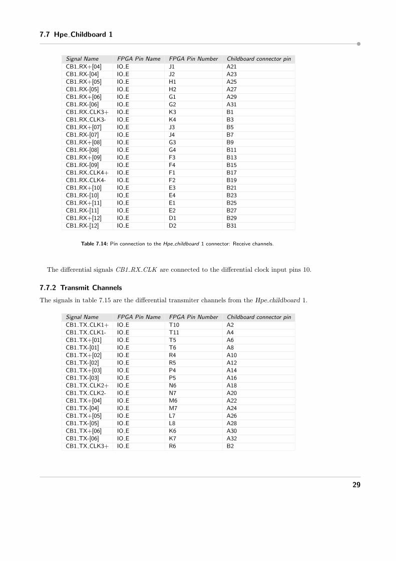
The differential signals CB1 RX CLK are connected to the differential clock input pins 10.
7.7.2 Transmit Channels
The signals in table 7.15 are the differential transmiter channels from the Hpe childboard 1.
Signal Name FPGA Pin Name FPGA Pin Number Childboard connector pin
CB1 TX CLK1+ IO E T10 A2
CB1 TX CLK1- IO E T11 A4
CB1 TX+[01] IO E T5 A6
CB1 TX-[01] IO E T6 A8
CB1 TX+[02] IO E R4 A10
CB1 TX-[02] IO E R5 A12
CB1 TX+[03] IO E P4 A14
CB1 TX-[03] IO E P5 A16
CB1 TX CLK2+ IO E N6 A18
CB1 TX CLK2- IO E N7 A20
CB1 TX+[04] IO E M6 A22
CB1 TX-[04] IO E M7 A24
CB1 TX+[05] IO E L7 A26
CB1 TX-[05] IO E L8 A28
CB1 TX+[06] IO E K6 A30
CB1 TX-[06] IO E K7 A32
CB1 TX CLK3+ IO E R6 B2
29

7 DUT-FPGA
Signal Name FPGA Pin Name FPGA Pin Number Childboard connector pin
CB1 TX CLK3- IO E R7 B4
CB1 TX+[07] IO E P6 B6
CB1 TX-[07] IO E P7 B8
CB1 TX+[08] IO E N8 B10
CB1 TX-[08] IO E N9 B12
CB1 TX+[09] IO E M8 B14
CB1 TX-[09] IO E M9 B16
CB1 TX CLK4+ IO E L9 B18
CB1 TX CLK4- IO E L10 B20
CB1 TX+[10] IO E K8 B22
CB1 TX-[10] IO E K9 B24
CB1 TX+[11] IO E J8 B26
CB1 TX-[11] IO E J9 B28
CB1 TX+[12] IO E J6 B30
CB1 TX-[12] IO E J7 B32
Table 7.15: Pin connection to the Hpe childboard 1 connector: Transmit channels
7.7.3 Configuration Pins for the DUT-FPGA#1 by the Hpe Childboard 1
The signals in table 7.16 can also be reached by the Clock Factory . Only the signals CB1 DATA[0]to CB1 DATA[7] can be used as normal I/O pins. The others are only for configuration.
Signal Name FPGA Pin Name FPGA Pin Number Childboard connector pin
CB1 CONFIG# nCONFIG AL30 A62
CB1 CONF DONE CONF DONE J25 A56
CB1 DATA[0] DATA0 H19 A53
CB1 DATA[1] DATA1 F20 A55
CB1 DATA[2] DATA2 G23 A57
CB1 DATA[3] DATA3 H23 A59
CB1 DATA[4] DATA4 J23 A61
CB1 DATA[5] DATA5 L22 A63
CB1 DATA[6] DATA6 F24 A65
CB1 DATA[7] DATA7 G24 A54
CB1 DCLK DCLK B31 A60
CB1 STATUS# nSTATUS B30 A58
Table 7.16: Pin connection to the Hpe childboard 1 connector: Configuration pins for the DUT-FPGA#1 .
7.7.4 Other pins
Table 7.17 gives you an overview of all other signals connected to the Hpe childboard 1.
Signal Name FPGA Pin Name FPGA Pin Number Childboard connector pin
CB1 CLK+ PLL12 OUT0p AL18 A49
CB1 CLK- PLL12 OUT0n AK18 A50
30

7.8 Hpe Childboard 2
Signal Name FPGA Pin Name FPGA Pin Number Childboard connector pin
CB1 TEST[0] IO F U6 B56
CB1 TEST[1] IO F U5 B57
CB1 TEST[2] IO F V5 B58
CB1 TEST[3] IO F V4 B59
CB1 EN TEST#[0] IO F W1 B60
CB1 EN TEST#[1] IO F V2 B61
CB1 EN TEST#[2] IO F V3 B62
CB1 EN TEST#[3] IO F W2 B63
CB1 RFU[0] IO F Y2 B64
CB1 RFU[1] IO F W4 B65
CB1 RFU[2] IO F W5 B66
Table 7.17: Pin connection to the Hpe childboard 1 connector: Other pins
The differential signals CB1 CLK* are connected to PLL output pins of the PLL 12.
7.8 Hpe Childboard 2
Table 7.18 lists all signals connected to this Hpe childboard.
Signal Name FPGA Pin Name FPGA Pin Number Childboard connector pin
CB2 BUS[0] IO H AK28 A1
CB2 BUS[1] IO H AK29 A2
CB2 BUS[2] IO H AM29 A3
CB2 BUS[3] IO H AL29 A4
CB2 BUS[4] IO H AK27 A5
CB2 BUS[5] IO H AJ27 A6
CB2 BUS[6] IO H AL25 A7
CB2 BUS[7] IO H AL26 A8
CB2 BUS[8] IO H AM25 A9
CB2 BUS[9] IO H AM26 A10
CB2 BUS[10] IO H AG24 A11
CB2 BUS[11] IO H AH26 A12
CB2 BUS[12] IO H AL23 A13
CB2 BUS[13] IO H AL24 A14
CB2 BUS[14] IO H AK23 A15
CB2 BUS[15] IO H AM23 A16
CB2 BUS[16] IO H AG23 A17
CB2 BUS[17] IO H AG22 A18
CB2 BUS[18] IO H AL21 A19
CB2 BUS[19] IO H AL22 A20
CB2 BUS[20] IO H AK21 A21
CB2 BUS[21] IO H AM21 A22
CB2 BUS[22] IO H AH20 A23
CB2 BUS[23] IO H AJ19 A24
CB2 BUS[24] IO H AE22 A25
CB2 BUS[25] IO H AF22 A26
CB2 BUS[26] IO H AG20 A27
CB2 BUS[27] IO H AB21 A28
31

7 DUT-FPGA
Signal Name FPGA Pin Name FPGA Pin Number Childboard connector pin
CB2 BUS[28] IO H AF20 A29
CB2 BUS[29] IO H AB20 A30
CB2 BUS[30] PLL5 FBp/OUT2p AL15 A31
CB2 BUS[31] PLL5 FBn/OUT2n AK15 A32
CB2 BUS[32] IO H AH28 B1
CB2 BUS[33] IO H AJ28 B2
CB2 BUS[34] IO H AL27 B3
CB2 BUS[35] IO H AL28 B4
CB2 BUS[36] IO H AM28 B5
CB2 BUS[37] IO H AM27 B6
CB2 BUS[38] IO H AK26 B7
CB2 BUS[39] IO H AJ26 B8
CB2 BUS[40] IO H AJ25 B9
CB2 BUS[41] IO H AH25 B10
CB2 BUS[42] IO H AH24 B11
CB2 BUS[43] IO H AK25 B12
CB2 BUS[44] IO H AM24 B13
CB2 BUS[45] IO H AK24 B14
CB2 BUS[46] IO H AJ22 B15
CB2 BUS[47] IO H AH22 B16
CB2 BUS[48] IO H AK22 B17
CB2 BUS[49] IO H AJ23 B18
CB2 BUS[50] IO H AM22 B19
CB2 BUS[51] IO H AJ21 B20
CB2 BUS[52] IO H AK20 B21
CB2 BUS[53] IO H AJ20 B22
CB2 BUS[54] IO H AH19 B23
CB2 BUS[55] IO H AL20 B24
CB2 BUS[56] IO H AD22 B25
CB2 BUS[57] IO H AF21 B26
CB2 BUS[58] IO H AD21 B27
CB2 BUS[59] IO H AC21 B28
CB2 BUS[60] IO H AD20 B29
CB2 BUS[61] IO H AC20 B30
CB2 BUS[62] PLL5 OUT0p B15 B31
CB2 BUS[62] PLL11 FBp/OUT2p AK16 B31
CB2 BUS[63] PLL5 OUT0n C15 B32
CB2 BUS[63] PLL11 FBn/OUT2n AJ16 B32
CB2 CLK+ PLL5 OUT1p AJ15 A49
CB2 CLK- PLL5 OUT1n AH15 A50
CB2 IO[0] IO H AJ11 A53
CB2 IO[1] IO H AH9 A54
CB2 IO[2] IO G AK11 A55
CB2 IO[3] IO G AH8 A56
CB2 IO[4] IO G AF12 A57
CB2 IO[5] IO G AK7 A58
CB2 IO[6] IO G AJ12 A59
CB2 IO[7] IO G AH7 A60
CB2 IO[8] IO G AK12 A61
CB2 IO[9] IO G AJ6 A62
CB2 IO[10] IO H AJ13 A63
32

7.9 Connector to the Mainboard
Signal Name FPGA Pin Name FPGA Pin Number Childboard connector pin
CB2 IO[11] IO G AK5 A64
CB2 IO[12] IO G AK13 A65
CB2 IO[13] IO G AH5 A66
CB2 IO[14] IO H AB19 B34
CB2 IO[15] IO H AE11 B49
CB2 IO[16] IO H AH11 B50
CB2 IO[17] IO H AF10 B51
CB2 IO[18] IO H AK10 B52
CB2 IO[19] IO H AE10 B53
CB2 IO[20] IO H AJ10 B54
CB2 IO[21] IO G AG9 B55
CB2 IO[22] IO G AG11 B56
CB2 IO[23] IO G AG8 B57
CB2 IO[24] IO G AK9 B58
CB2 IO[25] IO G AJ7 B59
CB2 IO[26] IO G AK8 B60
CB2 IO[27] IO H AK6 B61
CB2 IO[28] IO H AJ8 B62
CB2 IO[29] IO G AH6 B63
CB2 IO[30] IO G AF11 B64
CB2 IO[31] IO G AJ5 B65
CB2 IO[32] IO G AG10 B66
Table 7.18: Pin connection to the Hpe childboard 2 connector.
Additionally to the signal CB2 CLK* there are two more differential pairs: CB2 BUS[30]and CB2 BUS[31] is one differential signal pair where CB2 BUS[30] is the positive part andCB2 BUS[62] and CB2 BUS[63] is the other dirrerential signal pair where CB2 BUS[62] is thepositive part. The differential signals are connected to PLL output pins of the PLL 5. The signalpair CB2 BUS[62]/CB2 BUS[63] is additionally connected to the feedback pin of PLL 11.
7.9 Connector to the Mainboard
The following description is based on the presumption that the Hpe midi is used as a mainboard.For a detailed description of the pins, refer to the manual of the Hpe midi.
7.9.1 Hpe Childboard 3
Table 7.19 lists all signals connected to this Hpe childboard on the mainboard. The signalswhich are emphasised in the table (CB3 DATA[88] to CB3 DATA[96]) are only available whenthe EP2S180F1020C3N or the EP2S90F1020C3N is used. If the EP2S60F1020C3N is populated,then these signals are not connected on the FPGA.
Signal Name FPGA Pin Name FPGA Pin Number Childboard connector pin
CB3 CLK+ PLL11 OUT1p D18 A49
CB3 CLK- PLL11 OUT1n E18 A50
CB3 DATA[0] ASDO AB12 A1
CB3 DATA[1] nCSO AF4 A2
33

7 DUT-FPGA
Signal Name FPGA Pin Name FPGA Pin Number Childboard connector pin
CB3 DATA[2] CS L15 B1
CB3 DATA[3] nCS H21 B2
CB3 DATA[4] nWS F22 A3
CB3 DATA[5] nRS T23 A4
CB3 DATA[6] IO G C24 B3
CB3 DATA[7] IO G A24 B4
CB3 DATA[8] IO G D27 A5
CB3 DATA[9] IO G B22 A6
CB3 DATA[10] IO G A22 B5
CB3 DATA[11] IO G B21 B6
CB3 DATA[12] IO G B17 A7
CB3 DATA[13] IO G B16 A8
CB3 DATA[14] IO G E19 B7
CB3 DATA[15] IO G A14 B8
CB3 DATA[16] IO G E14 A9
CB3 DATA[17] IO G F17 A10
CB3 DATA[18] IO G J19 B9
CB3 DATA[19] IO G D5 B10
CB3 DATA[20] IO G G11 A11
CB3 DATA[21] IO G U22 A12
CB3 DATA[22] IO G V23 B11
CB3 DATA[23] IO G W25 B12
CB3 DATA[24] IO G AB16 A13
CB3 DATA[25] IO G AD14 A14
CB3 DATA[26] IO G AB10 B13
CB3 DATA[27] IO G K20 B14
CB3 DATA[28] IO G G22 A15
CB3 DATA[29] IO G L19 A16
CB3 DATA[30] IO G E27 B15
CB3 DATA[31] IO G AL8 B16
CB3 DATA[32] IO G AM7 A17
CB3 DATA[33] IO G AL7 A18
CB3 DATA[34] IO G AM6 B17
CB3 DATA[35] CLK6n AL6 B18
CB3 DATA[36] RUP7 AM5 A19
CB3 DATA[37] RDN7 AL5 A20
CB3 DATA[38] IO/TX56n V10 B19
CB3 DATA[39] IO/TX58p AL4 B20
CB3 DATA[40] IO/TX58n AK4 A21
CB3 DATA[41] IO/TX57p AM4 A22
CB3 DATA[42] IO/TX57n U10 B21
CB3 DATA[43] IO/TX52p U23 B22
CB3 DATA[44] IO/TX52n AE1 A23
CB3 DATA[45] IO/TX55p AF2 A24
CB3 DATA[46] IO/TX55n AH1 B23
CB3 DATA[47] IO/TX54p K30 B24
CB3 DATA[48] IO/TX54n H29 A25
CB3 DATA[49] IO/TX51p H30 A26
CB3 DATA[50] IO/TX51n G30 B25
CB3 DATA[51] IO/TX50p C29 B26
CB3 DATA[52] IO/TX50n D28 A27
34

7.9 Connector to the Mainboard
Signal Name FPGA Pin Name FPGA Pin Number Childboard connector pin
CB3 DATA[53] IO/TX49p D26 A28
CB3 DATA[54] IO/TX49n C26 B27
CB3 DATA[55] IO/TX45p C25 B28
CB3 DATA[56] IO/TX45n D22 A29
CB3 DATA[57] IO/TX48p F23 A30
CB3 DATA[58] IO/TX48n E22 B29
CB3 DATA[59] IO/TX46p C22 B30
CB3 DATA[60] IO/TX46n F15 A31
CB3 DATA[61] IO/TX47p F16 A32
CB3 DATA[62] IO/TX47n D14 B31
CB3 DATA[63] IO/TX44p C12 B32
CB3 DATA[64] IO/TX44n D12 B34
CB3 DATA[65] IO/TX43p F9 B49
CB3 DATA[66] IO/TX43n E9 B50
CB3 DATA[67] IO C C8 B51
CB3 DATA[68] IO C AC22 B52
CB3 DATA[69] IO C W32 A53
CB3 DATA[70] IO C V31 A54
CB3 DATA[71] IO C AB31 B53
CB3 DATA[72] IO C AB32 B54
CB3 DATA[73] IO C AG13 A55
CB3 DATA[74] IO C AG31 A56
CB3 DATA[75] IO C AG12 B55
CB3 DATA[76] IO C AH31 B56
CB3 DATA[77] IO C AF19 A57
CB3 DATA[78] IO C AE26 A58
CB3 DATA[79] IO C AC18 B57
CB3 DATA[80] IO C AE13 B58
CB3 DATA[81] IO C AH4 A59
CB3 DATA[82] CLK0n AB13 A60
CB3 DATA[83] CLK14n AE4 B59
CB3 DATA[84] CLK12n AC12 B60
CB3 DATA[85] CLK13n AB5 A61
CB3 DATA[86] RUP4 AD12 A62
CB3 DATA[87] RDN4 AB11 B61
CB3 DATA[88] NC/IO W22 B62
CB3 DATA[89] NC/IO W11 A63
CB3 DATA[90] NC/IO W10 A64
CB3 DATA[91] NC/IO AE6 B63
CB3 DATA[92] NC/IO AE5 B64
CB3 DATA[93] NC/IO AD4 A65
CB3 DATA[94] NC/IO AC30 A66
CB3 DATA[95] NC/IO AD30 B65
CB3 DATA[96] NC/IO AD29 B66
Table 7.19: Pin connection to the module connector: Hpe childboard 3 connector.
The differential signals CB3 CLK* are connected to PLL output pins of the PLL 11.
35

7 DUT-FPGA
7.9.2 Hpe Childboard 4
Table 7.20 lists all signals connected to this Hpe childboard on the mainboard.
Signal Name FPGA Pin Name FPGA Pin Number Childboard connector pin
CB4 CLK+ PLL12 FBp/OUT2p AM19 A49
CB4 CLK- PLL12 FBn/OUT2n AL19 A50
CB4 DATA[0] IO F M23 A1
CB4 DATA[1] IO F H27 A2
CB4 DATA[2] IO F L23 B1
CB4 DATA[3] IO F L26 B2
CB4 DATA[4] IO F J26 A3
CB4 DATA[5] IO F K25 A4
CB4 DATA[6] IO F N22 B3
CB4 DATA[7] IO F G29 B4
CB4 DATA[8] IO F K22 A5
CB4 DATA[9] IO F L25 A6
CB4 DATA[10] IO F L21 B5
CB4 DATA[11] IO F K24 B6
CB4 DATA[12] IO F M22 A7
CB4 DATA[13] IO F E29 A8
CB4 DATA[14] IO F K21 B7
CB4 DATA[15] IO F J21 B8
CB4 DATA[16] IO F J22 A9
CB4 DATA[17] IO F C28 A10
CB4 DATA[18] IO F L20 B9
CB4 DATA[19] IO F H22 B10
CB4 DATA[20] IO F AM10 A11
CB4 DATA[21] IO F AC4 A12
CB4 DATA[22] IO F AM9 B11
CB4 DATA[23] IO F AM8 B12
CB4 DATA[24] IO F A21 A13
CB4 DATA[25] IO F H11 A14
CB4 DATA[26] IO F F11 B13
CB4 DATA[27] IO F J11 B14
CB4 DATA[28] IO F G10 A15
CB4 DATA[29] IO F K11 A16
CB4 DATA[30] IO F W24 B15
CB4 DATA[31] IO F U27 B16
CB4 DATA[32] IO F Y25 A17
CB4 DATA[33] IO F V28 A18
CB4 DATA[34] IO F Y24 B17
CB4 DATA[35] IO F V29 B18
CB4 DATA[36] IO F AA25 A19
CB4 DATA[37] IO F W28 A20
CB4 DATA[38] IO F AA24 B19
CB4 DATA[39] IO F W29 B20
CB4 DATA[40] IO F AA23 A21
CB4 DATA[41] IO F Y28 A22
CB4 DATA[42] IO F AB25 B21
CB4 DATA[43] IO F Y29 B22
CB4 DATA[44] IO F AB23 A23
36

7.9 Connector to the Mainboard
Signal Name FPGA Pin Name FPGA Pin Number Childboard connector pin
CB4 DATA[45] IO F Y30 A24
CB4 DATA[46] IO F AE21 B23
CB4 DATA[47] IO F AA27 B24
CB4 DATA[48] IO F AE20 A25
CB4 DATA[49] IO F T22 A26
CB4 DATA[50] IO F AC19 B25
CB4 DATA[51] IO F V24 B26
CB4 DATA[52] IO F AE19 A27
CB4 DATA[53] IO F W27 A28
CB4 DATA[54] IO F AC9 B27
CB4 DATA[55] IO F AG18 B28
CB4 DATA[56] IO F AD10 A29
CB4 DATA[57] IO F AD18 A30
CB4 DATA[58] IO F AC11 B29
CB4 DATA[59] IO F AG15 B30
CB4 DATA[60] IO F AD11 A31
CB4 DATA[61] IO F AH14 A32
CB4 DATA[62] IO F AE12 B31
CB4 DATA[63] IO F AG14 B32
CB4 DATA[64] IO F AF13 B34
CB4 DATA[65] IO F AH29 B49
CB4 DATA[66] IO F AF23 B50
CB4 DATA[67] IO G AH30 B51
CB4 DATA[68] IO G AE23 B52
CB4 DATA[69] IO G AH13 A53
CB4 DATA[70] IO G AG32 A54
CB4 DATA[71] IO G AC16 B53
CB4 DATA[72] IO G AH32 B54
CB4 DATA[73] IO G AB15 A55
CB4 DATA[74] IO G AJ32 A56
CB4 DATA[75] IO G AC15 B55
CB4 DATA[76] IO G AJ31 B56
CB4 DATA[77] IO G AB14 A57
CB4 DATA[78] IO G AD19 A58
CB4 DATA[79] IO G AC14 B57
CB4 DATA[80] IO G AB18 B58
CB4 DATA[81] IO G AD13 A59
CB4 DATA[82] IO G AB17 A60
CB4 DATA[83] IO G AC13 B59
CB4 DATA[84] IO G AC17 B60
CB4 DATA[85] IO G AE14 A61
CB4 DATA[86] IO G AJ14 A62
CB4 DATA[87] IO G AL16 B61
CB4 DATA[88] IO G AM14 B62
CB4 DATA[89] IO G AL14 A63
CB4 DATA[90] IO G AL12 A64
CB4 DATA[91] IO G AL13 B63
CB4 DATA[92] IO G AL11 B64
CB4 DATA[93] IO G AM12 A65
CB4 DATA[94] IO G AL10 A66
CB4 DATA[95] IO G AM11 B65
37

7 DUT-FPGA
Signal Name FPGA Pin Name FPGA Pin Number Childboard connector pin
CB4 DATA[96] IO G AL9 B66
Table 7.20: Pin connection to the module connector: Hpe childboard 4 connector.
The differential signals CB4 CLK* are connected to PLL output pins of the PLL 11.
7.9.3 Audio Interface (AC97)
The signals in table 7.21 are connected to the AC97 on the mainboard.
Signal Name FPGA Pin Name FPGA Pin Number
AC97 BITCLK CLK0p T32
AC97 EAPD IO/TX60n AC24
AC97 EXT CLK PLL12 OUT1p AJ18
AC97 RESET# IO/TX59n AC7
AC97 SDATA IN IO/TX56p AC8
AC97 SDATA OUT IO/TX59p AD25
AC97 SYNC IO/TX60p AD24
Table 7.21: Pin connection to the module connector: AC97.
The signal AC97 EXT CLK is connected to a PLL output pin of the PLL 12. The signalAC97 BITCLK is connected to the clock input pin 0.
7.9.4 A/D Converter (ADC) and D/A Converter (DAC)
The signals in table 7.22 are connected to the ADC/DAC on the mainboard.
Signal Name FPGA Pin Name FPGA Pin Number
ADC AIN IO C AE25
ADC DOUT IO C E25
ADC DOUT# IO C J20
DAC OUT IO C AD9
Table 7.22: Pin connection to the module connector: ADC/DAC.
7.9.5 CAN Interface
The signals in table 7.23 are connected to the CAN on the mainboard.
Signal Name FPGA Pin Name FPGA Pin Number
CAN RXD IO C Y5
CAN STB IO C Y6
CAN TXD IO C AA8
38

7.9 Connector to the Mainboard
Table 7.23: Pin connection to the module connector: CAN.
7.9.6 External User Interface
The signals in table 7.24 are connected to the external user interface on the mainboard.
Signal Name FPGA Pin Name FPGA Pin Number
DSW[0] IO/RX53p W31
DSW[1] IO/RX53n Y31
DSW[2] IO/RX51p AA32
DSW[3] IO/RX51n AA31
DSW[4] IO/RX52p AC32
DSW[5] IO/RX52n AC31
DSW[6] IO/RX47p AD32
DSW[7] IO/RX47n AD31
Table 7.24: Pin connection to the module connector: external user interface.
7.9.7 Ethernet Interface
The signals in table 7.25 are connected to the ethernet on the mainboard.
Signal Name FPGA Pin Name FPGA Pin Number
ETH COL IO/RX61p U11
ETH CRS IO/RX56n AG2
ETH MDC IO/RX54n AH2
ETH MDINTR# IO/RX54p AJ2
ETH MDIO IO/RX59p AJ1
ETH RESET# IO/RX59n AH3
ETH RXCLK CLK13p E16
ETH RXDV IO/RX56p AG1
ETH RXD[0] IO/RX60n AE2
ETH RXD[1] IO/RX60p AD2
ETH RXD[2] IO/RX55n AD1
ETH RXD[3] IO/RX55p AC2
ETH RXER IO/RX61n AB1
ETH TXCLK CLK12p A16
ETH TXD[0] IO/RX63p AC1
ETH TXD[1] IO/RX57n AB2
ETH TXD[2] IO/RX57p AA2
ETH TXD[3] IO/RX62n AA1
ETH TXEN IO/RX63n AF1
ETH TXER IO/RX62p Y3
Table 7.25: Pin connection to the module connector: ethernet.
39

7 DUT-FPGA
The signal ETH TXCLK is connected to the clock input pin 12 and the signal ETH RXCLKis connected to the clock input pin 13.
7.9.8 Expansion Connector
The signals in table 7.26 are connected to the expansion connector on the mainboard.
Signal Name FPGA Pin Name FPGA Pin Number
EXPCON CLKIN PLL12 OUT1n AH18
EXPCON CLKOUT CLK2n U31
Table 7.26: Pin connection to the module connector: expansion connector.
7.9.9 Parallel Flash
The signals in table 7.27 are connected to the flash on the mainboard.
Signal Name FPGA Pin Name FPGA Pin Number
FLASH BYTE# IO D C23
FLASH CE# IO D C21
FLASH RESET# IO D D23
FLASH RY/BY# A IO D E20
FLASH RY/BY# B IO D D20
FLASH WP#/ACC IO D E24
Table 7.27: Pin connection to the module connector: flash.
7.9.10 Human Interface
The signals in table 7.28 are connected to the 7-segment display, DIP switches and LEDs on themainboard.
Signal Name FPGA Pin Name FPGA Pin Number
HUMI A# IO/TX64p D32
HUMI B# IO/TX64n F30
HUMI C# IO/TX62p B29
HUMI D# IO/TX62n D31
HUMI E# IO/TX63p A29
HUMI F# IO/TX63n F29
HUMI G# IO/TX61p A28
HUMI DP# IO/TX61n B28
HUMI LED# IO/RX44n Y11
HUMI SEG0# IO/RX43p B27
HUMI SEG1# IO/RX43n E30
Table 7.28: Pin connection to the module connector: human interface.
40

7.9 Connector to the Mainboard
7.9.11 I2C
The signals in table 7.29 are connected to the I2C on the mainboard.
Signal Name FPGA Pin Name FPGA Pin Number
I2C SCL[1] IO A AB4
I2C SDA[1] IO A AC3
Table 7.29: Pin connection to the module connector: I2C.
7.9.12 LCD Connector
The signals in table 7.30 are connected to the LCD on the mainboard.
Signal Name FPGA Pin Name FPGA Pin Number
LCD ENABLE IO D A23
LCD REGSEL IO D B23
LCD RW IO D D25
Table 7.30: Pin connection to the module connector: LCD.
7.9.13 LIN Interface
The signals in table 7.31 are connected to the LIN on the mainboard.
Signal Name FPGA Pin Name FPGA Pin Number
LIN ACTIVE# IO C AG3
LIN RXD IO C AD6
LIN SLP# IO C AG4
LIN TXD IO C AA22
Table 7.31: Pin connection to the module connector: LIN.
7.9.14 Memory
The signals in table 7.32 are connected to the memories on the mainboard.
Signal Name FPGA Pin Name FPGA Pin Number
MEMORY A[0] IO D E13
MEMORY A[1] IO D L17
MEMORY A[2] IO D K17
MEMORY A[3] IO D L13
41

7 DUT-FPGA
Signal Name FPGA Pin Name FPGA Pin Number
MEMORY A[4] IO D L16
MEMORY A[5] IO D J13
MEMORY A[6] IO D D11
MEMORY A[7] IO D K16
MEMORY A[8] IO D J15
MEMORY A[9] IO D K13
MEMORY A[10] IO D D10
MEMORY A[11] IO D K15
MEMORY A[12] IO D H14
MEMORY A[13] IO D J12
MEMORY A[14] IO D J14
MEMORY A[15] IO D K12
MEMORY A[16] IO D E8
MEMORY A[17] IO D G13
MEMORY A[18] IO D H13
MEMORY A[19] IO D L12
MEMORY A[20] IO D E7
MEMORY A[21] IO D G12
MEMORY A[22] IO D H12
MEMORY DQ[0] IO C A12
MEMORY DQ[1] IO C B13
MEMORY DQ[2] IO C B11
MEMORY DQ[3] IO C D13
MEMORY DQ[4] IO C A11
MEMORY DQ[5] IO C F12
MEMORY DQ[6] IO C B10
MEMORY DQ[7] IO C C11
MEMORY DQ[8] IO C A10
MEMORY DQ[9] IO C E11
MEMORY DQ[10] IO C B9
MEMORY DQ[11] IO C C10
MEMORY DQ[12] IO C A9
MEMORY DQ[13] IO C F10
MEMORY DQ[14] IO C B8
MEMORY DQ[15] IO C C9
MEMORY DQ[16] IO C A8
MEMORY DQ[17] IO C D8
MEMORY DQ[18] IO C B7
MEMORY DQ[19] IO C C7
MEMORY DQ[20] IO C A7
MEMORY DQ[21] IO C D7
MEMORY DQ[22] IO C B6
MEMORY DQ[23] IO C C6
MEMORY DQ[24] IO C A6
MEMORY DQ[25] IO C D6
MEMORY DQ[26] IO C B5
MEMORY DQ[27] IO C E6
MEMORY DQ[28] IO C A5
MEMORY DQ[29] IO C C5
MEMORY DQ[30] IO C C4
MEMORY DQ[31] IO C E5
42

7.9 Connector to the Mainboard
Signal Name FPGA Pin Name FPGA Pin Number
MEMORY OE# IO D B14
MEMORY WE# IO D D19
Table 7.32: Pin connection to the module connector: memories.
7.9.15 PS/2 Ports
The signals in table 7.33 are connected to the PS/2 on the mainboard.
Signal Name FPGA Pin Name FPGA Pin Number
PS2 KBCLK PLL6 OUT0p B15
PS2 KBDAT PLL6 OUT0n C15
PS2 MCLK PLL6 OUT1p C16
PS2 MDAT PLL6 OUT1n D16
Table 7.33: Pin connection to the module connector: PS/2.
The signals PS2 KBCLK and PS2 MCLK are connected to PLL output pins of the PLL 6.
7.9.16 Serial Interface (RS232)
The signals in table 7.34 are connected to the RS232 on the mainboard.
Signal Name FPGA Pin Name FPGA Pin Number
RS0 CTS LVTTL IO D Y9
RS0 RTS LVTTL IO D AA4
RS0 RXD LVTTL IO D AB3
RS0 TXD LVTTL IO D AB9
RS1 CTS LVTTL IO D AB8
RS1 RTS LVTTL IO D Y4
RS1 RXD LVTTL IO D AA3
RS1 TXD LVTTL IO D W9
Table 7.34: Pin connection to the module connector: RS232.
7.9.17 SD Card Reader
The signals in table 7.35 are connected to the SD card on the mainboard.
Signal Name FPGA Pin Name FPGA Pin Number
SDCARD CD IO D K18
SDCARD CS IO D G21
SDCARD CT IO D L18
SDCARD DAT IO D G19
43

7 DUT-FPGA
SDCARD DI IO D H20
SDCARD DO IO D K19
SDCARD IRQ IO D L14
SDCARD SCLK IO D D21
SDCARD WRP IO D K14
Table 7.35: Pin connection to the module connector: SD card.
7.9.18 Asynchronous SRAM
The signals in table 7.36 are connected to the SRAM on the mainboard.
Signal Name FPGA Pin Name FPGA Pin Number
SRAM BE0# IO D C13
SRAM BE1# IO D F14
SRAM BE2# IO D B12
SRAM BE3# IO D F13
SRAM CEn IO D B20
Table 7.36: Pin connection to the module connector: SRAM.
7.9.19 3 x 4 Key Matrix
The signals in table 7.37 are connected to the key matrix on the mainboard.
Signal Name FPGA Pin Name FPGA Pin Number
TST COL[0] IORX48n B24
TST COL[1] IO/RX46p E28
TST COL[2] IO/RX46n A26
TST COL[3] IO/RX49p C27
TST COL[4] IO/RX49n A25
TST COL[5] IO/RX44p B25
TST ROW[0] IO/RX50n AE32
TST ROW[1] IO/RX45p AE31
TST ROW[2] IO/RX45n AF32
TST ROW[3] IO/RX48p AF31
TST STEP IO/RX50p E26
Table 7.37: Pin connection to the module connector: key matrix.
7.9.20 USB Target Connector
The signals in table 7.38 are connected to the USB target for debugging on the mainboard.
44

7.9 Connector to the Mainboard
Signal Name FPGA Pin Name FPGA Pin Number
USBD CLKOUT CLK2p U32
USBD DBUS16 8 IO A E31
USBD D[0] IO A T31
USBD D[1] IO A N30
USBD D[2] IO A R31
USBD D[3] IO A N29
USBD D[4] IO A R30
USBD D[5] IO A N28
USBD D[6] IO A P31
USBD D[7] IO A P32
USBD D[8] IO A N31
USBD D[9] IO A M29
USBD D[10] IO A M31
USBD D[11] IO A M32
USBD D[12] IO A L32
USBD D[13] IO A M27
USBD D[14] IO A K32
USBD D[15] IO A L31
USBD LINESTATE[0] IO A G32
USBD LINESTATE[1] IO A F32
USBD OPMODE[0] IO A J27
USBD OPMODE[1] IO A E32
USBD RESET IO A A27
USBD RXACTIVE IO A H32
USBD RXERROR IO A J31
USBD RXVALID IO A L29
USBD SUSPEND IO A G31
USBD TERMSEL IO A K27
USBD TXREADY IO A J32
USBD TXVALID IO A K31
USBD UNIBIDI IO A H28
USBD VALIDH IO A F31
USBD VBUS IO A B26
USBD XCRSEL IO A H31
Table 7.38: Pin connection to the module connector: USB target.
The signal USBD CLKOUT is connected to the clock input pin 2.
7.9.21 USB Host and On The Go (OTG) Connector
The signals in table 7.39 are connected to the USB OTB on the mainboard.
Signal Name FPGA Pin Name FPGA Pin Number
USB CTS IO A AA7
USB GPIO[0] IO A AA29
USB GPIO[1] IO A W26
USB GPIO[2] IO A AA30
USB GPIO[3] IO A Y27
45

7 DUT-FPGA
Signal Name FPGA Pin Name FPGA Pin Number
USB GPIO[4] IO A AB28
USB GPIO[5] IO A Y26
USB GPIO[6] IO A AB29
USB GPIO[7] IO A AA26
USB GPIO[8] IO A AB30
USB GPIO[9] IO A AB27
USB GPIO[10] IO A AC26
USB GPIO[11] IO A AB26
USB GPIO[12] IO A AC27
USB GPIO[13] IO A AC25
USB GPIO[14] IO A AD27
USB GPIO[15] IO A AE28
USB GPIO[16] IO A AE29
USB GPIO[17] IO A AG29
USB GPIO[18] IO A AE30
USB GPIO[19] IO A AG30
USB GPIO[20] IO A AF30
USB GPIO[21] IO A AD26
USB GPIO[22] IO A AF29
USB GPIO[23] IO A AE27
USB GPIO[24] IO A AD8
USB GPIO[25] IO A AB24
USB GPIO[26] IO A AC6
USB GPIO[27] IO A Y23
USB GPIO[28] IO A AD7
USB MISO IO A AA6
USB MOSI IO A AB6
USB OC0# IO A Y8
USB OC1# IO A AA10
USB OC2# IO A Y7
USB OC3# IO A Y10
USB PWEN[0] IO A W6
USB PWEN[1] IO A AA9
USB PWEN[2] IO A Y22
USB PWEN[3] IO A AE3
USB RTS IO A W7
USB RXD IO A V6
USB SCK IO A W8
USB SCL IO A AA11
USB SDA IO A AF3
USB SSI# IO A AB7
USB TXD IO A V9
Table 7.39: Pin connection to the module connector: USB OTG.
7.9.22 VGA Interface
The signals in table 7.40 are connected to the VGA on the mainboard.
46

7.9 Connector to the Mainboard
Signal Name FPGA Pin Name FPGA Pin Number
VGA BLANK# IO D K26
VGA BL[0] IO C N27
VGA BL[1] IO C N25
VGA BL[2] IO D L30
VGA BL[3] IO D R22
VGA BL[4] IO D N26
VGA BL[5] IO D N24
VGA BL[6] IO D M26
VGA BL[7] IO D M24
VGA CLK IO D M25
VGA GR[0] IO C P28
VGA GR[1] IO C R24
VGA GR[2] IO D P27
VGA GR[3] IO D R23
VGA GR[4] IO D P26
VGA GR[5] IO D P25
VGA GR[6] IO D M30
VGA GR[7] IO D P24
VGA HSYNC IO D K29
VGA RD[0] IO C R29
VGA RD[1] IO C T28
VGA RD[2] IO D R28
VGA RD[3] IO D T27
VGA RD[4] IO D P29
VGA RD[5] IO D R25
VGA RD[6] IO D R26
VGA RD[7] IO D R27
VGA SYNC# IO D N23
VGA VSYNC IO D L24
Table 7.40: Pin connection to the module connector: VGA.
7.9.23 System Reset
The signals in table 7.41 are also connected to the mainboard.
Signal Name FPGA Pin Name FPGA Pin Number
CARDSEL# IO D C20
USER RESET# IO C U28
HPE RESOUT# IO C V30
Table 7.41: Pin connection to the module connector: Other pins.
Attention: When you use the USER RESET#, you have to add a pull up resistor into thePAD of the FPGA!
47

7 DUT-FPGA
7.9.24 Powerl Reset
The signal PWR RESET# table 7.42 is the global reset signal for the whole system. It isdelivered via the module connector.
Signal Name FPGA Pin Name FPGA Pin Number
PWR RESET# DEV CLRn AG19
Table 7.42: Pin connection to the module connector: Global Reset.
48
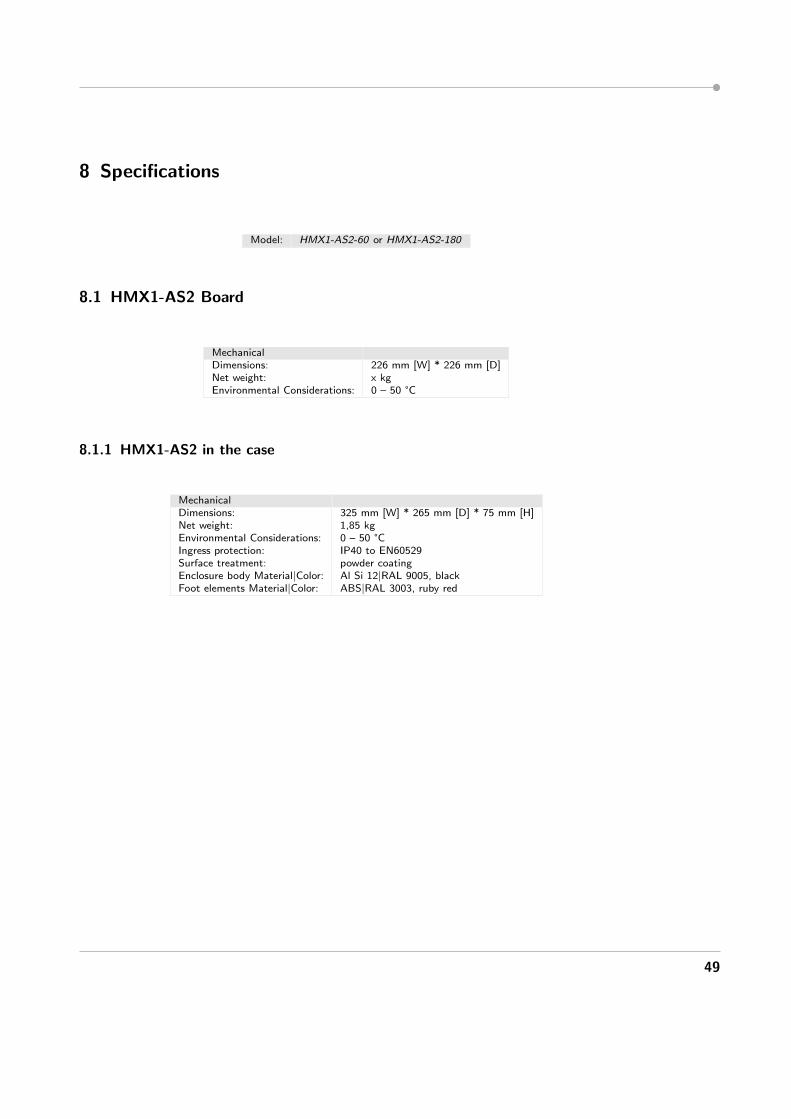
8 Specifications
Model: HMX1-AS2-60 or HMX1-AS2-180
8.1 HMX1-AS2 Board
MechanicalDimensions: 226 mm [W] * 226 mm [D]Net weight: x kgEnvironmental Considerations: 0 – 50 °C
8.1.1 HMX1-AS2 in the case
MechanicalDimensions: 325 mm [W] * 265 mm [D] * 75 mm [H]Net weight: 1,85 kgEnvironmental Considerations: 0 – 50 °CIngress protection: IP40 to EN60529Surface treatment: powder coatingEnclosure body Material|Color: Al Si 12|RAL 9005, blackFoot elements Material|Color: ABS|RAL 3003, ruby red
49

8 Specifications
50

9 Trouble Shooting
9.1 Testing the hardware
On the CD for the Hpe midi and the HMX1-AS2 there is a directory testing peripheralswhere some informations and data for the HMX1-AS2 module can be found.
9.1.1 Generell Information
This test is important for checking the module connection between the HMX1-AS2 and Hpe midi.It should always be started after removing the HMX1-AS2 and later on putting it back onto theHpe midi. Otherwise it’s possible that there is no good connection between them.
9.1.2 Software which is recommended for testing
1. Cygwin
2. Teraterm for Windows users
3. Minicom for Linux users
4. GRMON-eval which can be found on the CD. Here only the path must be set to theGRMON bin diectory
9.1.3 Testroutine started automatically
Start Teraterm or Minicom. Set the correct com options (38400 Baudrate, 8 databits, no parityand 1 stop bit).
Connect the cables (Ethernet, RS232 and VGA).
Load the .sof-file (can be found on the cd in the testing peripherals directory) into the FPGA.
Now the Sevensegment display should display L3 and most of the 8 LED’s below the Sev-ensegemnt display should light. Near the Ethernet connector a red LED should light. If not it’spossible that the cable has not put in correctly or that it take some time. This LED is a statusLED and shows that there is a connection between the pc and the Hpe midi.
At the Teraterm window the Hpe midi Testprogram should have been started automatically.With ESC you can move over the DAC and ADC test routines, if you don’t want to check them.Then the testroutine shows Hit a key to probe the interface, ¡ESC¿ to exit. At this phase ofthe test it’s possible to check, if the Keymatrix, the Sevensegment and the DIP-Switched are ok.Press a Key on the Keymatrix or change a postion of the DIP-Switches and afterwards pressenter on the keyboard of the pc connected to the Hpe midi. This will result in a change of theSevensegment display and the log in the Teraterm or Minicom window should look like Figure9.1 and 9.2. With ESC it’s possible to end the test routine.
51

9 Trouble Shooting
Figure 9.1: Leon3 testroutine output part 1
52

9.1 Testing the hardware
Figure 9.2: Leon3 testroutine output part 2
9.1.4 Starting the testroutine over Ethernet
Set the correct IP for later on connection to the Hpe midi over Ethernet (see Figure 9.3).
Start Cygwin or anything like this for later on testing. Move to the path on the CD wherethe hpe test.exe can be found. Enter the following line in the Cygwin window:
grmon-eval -eth -ip 192.168.25.90 -freq 40
Figure 9.3: IP-Address for the connection to the Hpe midi
53

9 Trouble Shooting
Figure 9.4: Ethernet connection to the Hpe midi
As result there should be an information displayed like in Figure 9.4.If not, then there is a problem with the ethernet connection and you should restart the testing
phase.
Enter the following line in the Cygwin window:lo hpe test.exe
Now the Testroutine has been downloaded into the RAM. And can be started with the runcommand in the cygwin window.
Enter the following line in the Cygwin window:run
The result should be the same as at the test started automatically.
What has been checked with this test routine:
54

9.1 Testing the hardware
1. Ethernet Connection
2. RS232 Connection
3. USB Memory
4. SRAM
5. Flash
6. Keymatrix
7. DIP-Switches
8. LCD-Display if connected
9. VGA
10. Sevensegment Display
11. 8 LED’s
55

INDEX
Index
SEmulator, 16, 283 x 4 Key Matrix, 44
A/D Converter (ADC) and D/A Converter (DAC),38
AES, 9Asynchronous SRAM, 44Audio Interface (AC97), 38
CAN Interface, 38Clock Distribution, 11Clock Factory, 11Clock from Oscillator, 28Clocks, 15, 24Configuration Pins, 26Configuration Pins for the DUT-FPGA#1 by
the CPLD for Clock Factory and Con-figuration, 23
Configuration Pins for the DUT-FPGA#1 bythe Hpe Childboard 1, 30
Configuration via Flash, 11Connector to the Mainboard, 33
Ethernet Interface, 39Expansion Connector, 40External User Interface, 39
Fan Control, 12Fast PLL Clock Inputs, 24FCP, 13
Global Reset, 15
HMX1-AS2 in the case, 49Hpe Childboard 1, 16, 28Hpe Childboard 2, 17, 31Hpe Childboard 3, 33Hpe Childboard 4, 36Hpe Childboard Connectors, 16Human Interface, 40
I2C, 41I/O Power, 21I/Os for Peripherals, 15
JTAG, 15JTAG configuration, 13JTAG Pins for internal JTAG Core, 27
LCD Connector, 41LEDs, 9LIN Interface, 41
Memory, 41Module Connectors, 15
Parallel Flash, 40PLL Output Clocks, 25PLLs, 23Power Control, 15Power Supply, 21PS/2 Ports, 43
Reset, 9
SD Card Reader, 43Serial Interface (RS232), 43Signal AC97 BITCLK, 38Signal AC97 EAPD, 38Signal AC97 EXT CLK, 38Signal AC97 RESET#, 38Signal AC97 SDATA IN, 38Signal AC97 SDATA OUT, 38Signal AC97 SYNC, 38Signal ADC AIN, 38Signal ADC DOUT, 38Signal ADC DOUT#, 38Signal CAN RXD, 38Signal CAN STB, 38Signal CAN TXD, 38Signal CARDSEL#, 47Signal CB1 CLK+, 30Signal CB1 CLK-, 30Signal CB1 CONF DONE, 30Signal CB1 CONFIG#, 30Signal CB1 DATA, 30Signal CB1 DCLK, 30Signal CB1 EN TEST#, 31
56

INDEX
Signal CB1 RFU, 31Signal CB1 RX+, 28, 29Signal CB1 RX-, 28, 29Signal CB1 RX CLK1+, 28Signal CB1 RX CLK1-, 28Signal CB1 RX CLK2+, 28Signal CB1 RX CLK2-, 28Signal CB1 RX CLK3+, 29Signal CB1 RX CLK3-, 29Signal CB1 RX CLK4+, 29Signal CB1 RX CLK4-, 29Signal CB1 STATUS#, 30Signal CB1 TEST, 31Signal CB1 TX+, 29, 30Signal CB1 TX-, 29, 30Signal CB1 TX CLK1+, 29Signal CB1 TX CLK1-, 29Signal CB1 TX CLK2+, 29Signal CB1 TX CLK2-, 29Signal CB1 TX CLK3+, 29Signal CB1 TX CLK3-, 30Signal CB1 TX CLK4+, 30Signal CB1 TX CLK4-, 30Signal CB2 BUS, 31, 32Signal CB2 CLK+, 32Signal CB2 CLK-, 32Signal CB2 IO, 32, 33Signal CB3 CLK+, 33Signal CB3 CLK-, 33Signal CB3 DATA, 33–35Signal CB4 CLK+, 36Signal CB4 CLK-, 36Signal CB4 DATA, 36–38Signal DAC OUT, 38Signal DSW, 39Signal DUT1 CLK100M, 28Signal DUT1 CLK14P, 24Signal DUT1 CLK15+, 24Signal DUT1 CLK15-, 24Signal DUT1 CLK1P, 24Signal DUT1 CLK3P, 24Signal DUT1 CLK4P, 24Signal DUT1 CLK5P, 24Signal DUT1 CLK6P, 24Signal DUT1 CLK7+, 24Signal DUT1 CLK7-, 24Signal DUT1 CLK8P, 24Signal DUT1 CLK9P, 24Signal DUT1 CLKUSR, 25
Signal DUT1 CRC ERROR, 25Signal DUT1 DEV OE, 25Signal DUT1 FPLL10N, 25Signal DUT1 FPLL10P, 25Signal DUT1 FPLL7N, 25Signal DUT1 FPLL7P, 25Signal DUT1 FPLL8N, 25Signal DUT1 FPLL8P, 25Signal DUT1 FPLL9N, 25Signal DUT1 FPLL9P, 25Signal DUT1 PLL11O1N, 25Signal DUT1 PLL11O1P, 25Signal DUT1 PLL6O2N, 25Signal DUT1 PLL6O2P, 25Signal DUT1 RDY# BSY, 25Signal DUT1 RU# LU, 25Signal ETH COL, 39Signal ETH CRS, 39Signal ETH MDC, 39Signal ETH MDINTR#, 39Signal ETH MDIO, 39Signal ETH RESET#, 39Signal ETH RXCLK, 39Signal ETH RXD, 39Signal ETH RXDV, 39Signal ETH RXER, 39Signal ETH TXCLK, 39Signal ETH TXD, 39Signal ETH TXEN, 39Signal ETH TXER, 39Signal EXPCON CLKIN, 40Signal EXPCON CLKOUT, 40Signal FLASH BYTE#, 40Signal FLASH CE#, 40Signal FLASH RESET#, 40Signal FLASH RY/BY# A, 40Signal FLASH RY/BY# B, 40Signal FLASH WP#/ACC, 40Signal HPE RESOUT#, 47Signal HUMI A#, 40Signal HUMI B#, 40Signal HUMI C#, 40Signal HUMI D#, 40Signal HUMI DP#, 40Signal HUMI E#, 40Signal HUMI F#, 40Signal HUMI G#, 40Signal HUMI LED#, 40Signal HUMI SEG0#, 40
57

INDEX
Signal HUMI SEG1#, 40Signal I2C SCL, 41Signal I2C SDA, 41Signal LCD ENABLE, 41Signal LCD REGSEL, 41Signal LCD RW, 41Signal LIN ACTIVE#, 41Signal LIN RXD, 41Signal LIN SLP#, 41Signal LIN TXD, 41Signal MEMORY A, 41, 42Signal MEMORY DQ, 42Signal MEMORY OE#, 43Signal MEMORY WE#, 43Signal PS2 KBCLK, 43Signal PS2 KBDAT, 43Signal PS2 MCLK, 43Signal PS2 MDAT, 43Signal PWR RESET#, 48Signal RS0 CTS LVTTL, 43Signal RS0 RTS LVTTL, 43Signal RS0 RXD LVTTL, 43Signal RS0 TXD LVTTL, 43Signal RS1 CTS LVTTL, 43Signal RS1 RTS LVTTL, 43Signal RS1 RXD LVTTL, 43Signal RS1 TXD LVTTL, 43Signal SDCARD CD, 43Signal SDCARD CS, 43Signal SDCARD CT, 43Signal SDCARD DAT, 43Signal SDCARD DI, 44Signal SDCARD DO, 44Signal SDCARD IRQ, 44Signal SDCARD SCLK, 44Signal SDCARD WRP, 44Signal SRAM BE0#, 44Signal SRAM BE1#, 44Signal SRAM BE2#, 44Signal SRAM BE3#, 44Signal SRAM CEn, 44Signal TST COL, 44Signal TST ROW, 44Signal TST STEP, 44Signal USB CTS, 45Signal USB GPIO, 45, 46Signal USB MISO, 46Signal USB MOSI, 46Signal USB OC0#, 46
Signal USB OC1#, 46Signal USB OC2#, 46Signal USB OC3#, 46Signal USB PWEN, 46Signal USB RTS, 46Signal USB RXD, 46Signal USB SCK, 46Signal USB SCL, 46Signal USB SDA, 46Signal USB SSI#, 46Signal USB TXD, 46Signal USBD CLKOUT, 45Signal USBD D, 45Signal USBD DBUS16 8, 45Signal USBD LINESTATE, 45Signal USBD OPMODE, 45Signal USBD RESET, 45Signal USBD RXACTIVE, 45Signal USBD RXERROR, 45Signal USBD RXVALID, 45Signal USBD SUSPEND, 45Signal USBD TERMSEL, 45Signal USBD TXREADY, 45Signal USBD TXVALID, 45Signal USBD UNIBIDI, 45Signal USBD VALIDH, 45Signal USBD VBUS, 45Signal USBD XCRSEL, 45Signal USER RESET#, 47Signal VGA BL, 47Signal VGA BLANK#, 47Signal VGA CLK, 47Signal VGA GR, 47Signal VGA HSYNC, 47Signal VGA RD, 47Signal VGA SYNC#, 47Signal VGA VSYNC, 47Software which is recommended for testing, 51Specifications, 49Starting the testroutine over Ethernet, 53System Overview, 7System Reset, 47
Trouble Shooting, 51
USB Host and On The Go (OTG) Connector,45
USB Target Connector, 44
VGA Interface, 46
58