usb io plus english - dan kohndankohn.info/projects/usbio_w_relay/usbio and relay/usb_io_plus... ·...
TRANSCRIPT

1
USBUSBUSBUSB____IOIOIOIO_Plus_Plus_Plus_Plus
DDDData ata ata ata AAAAcquisition cquisition cquisition cquisition DDDDeviceeviceeviceevice
IIII////OOOO & ADC & PWM & ADC & PWM & ADC & PWM & ADC & PWM(DAC)(DAC)(DAC)(DAC) & & & & CCCCounter & ounter & ounter & ounter & UARTUARTUARTUART
ppppcb8051@cb8051@cb8051@[email protected]

2
Features summaryFeatures summaryFeatures summaryFeatures summary::::
� Full-Speed USB 2.0 communication.
� Drivers available for Windows 2000/XP/Vista.
� Embedded command interpreter.
� 28 general purpose digital I/Os.
� 8 Analog Input Channels (10 bits ADC): ADC Range [0:1023].
� 4 Pulse Width Modulations: PWM Width Range [0:255].
� 4 Analog Output Channels: DAC Range [0:255].
� 2 Counters(16 bits Counter):Counter Range [0:65535].
� 2 UART:TX0/RX0 and TX1/RX1 support.
� Powers from USB (5 Voltage, maximum 500mA) .
� Provide Visual Basic 6.0 Test Program Source Code.(VB 6 testing
case)
USB data acquisition device control method is very easy for Windows
XP / Vista operating system. The simplest way is through the virtual Com
Port. Any existing software or programming environment that can send text
string to a COM port will know how to talk to the USB data acquisition
device. You can even perform simple tests with your favorite terminal
emulator. The product needs assembled and soldered by yourself.
Six functional modules, I/OI/OI/OI/O, ADCADCADCADC, PWMPWMPWMPWM, DACDACDACDAC, CounterCounterCounterCounter and UARTUARTUARTUART are
provided; the followings are the specifications for them.

3
USB Data Acquisition USB Data Acquisition USB Data Acquisition USB Data Acquisition DeviceDeviceDeviceDevice Pin Pin Pin Pin ddddefinitionefinitionefinitionefinition::::
IO PinIO PinIO PinIO Pin FunctionFunctionFunctionFunction IO PinIO PinIO PinIO Pin FunctionFunctionFunctionFunction
IO_10 IO10/TX1 IO_00 IO00/TX0
IO_11 IO11/RX1 IO_01 IO01/RX0
IO_12 IO12/Counter1 IO_02 IO02/Counter0
IO_13 IO13 IO_03 IO03
IO_14 IO14 IO_04 IO04
IO_15 IO!5 IO_05 IO05
IO_16 IO16 IO_06 IO06
IO_17 IO17 IO_07 IO07
IO_18 IO18/ADC4 IO_08 IO08/ADC0
IO_19 IO19/ADC5 IO_09 IO09/ADC1
IO_1A IO1A/ADC6 IO_0A IO0A/ADC2
IO_1B IO1B/ADC7 IO_0B IO0B/ADC3
IO_1C IO1C/PWM2 IO_0C IO0C/PWM0
IO_1D IO1D/PWM3 IO_0D IO0D/PWM1

4
USBUSBUSBUSB____IOIOIOIO DDDDeviceeviceeviceevice Control Command FormatControl Command FormatControl Command FormatControl Command Format::::
� Read the version of the USB_IO device firmware.
~ver~ ……………send to USB_IO
~VER:3.1~ ……………Receive from USB_IO
� 28 Digital Input/Output Ports: IO00~IO0D and IO10~IO1DIO00~IO0D and IO10~IO1DIO00~IO0D and IO10~IO1DIO00~IO0D and IO10~IO1D
~out00=1~ ………………send to USB_IO (IO00=’1’)
~OK~ ………………Receive from USB_IO
~out1A=0~ ………………Send to USB_IO (IO1A=’0’)
~OK~ ………………Receive from USB_IO
~in06~ ………………Send to USB_IO
~in06=0~ ………………Receive from USB_IO (IO06=’0’)
~in1A~ ………………Send to USB_IO
~in1A=1~ ………………Receive from USB_IO (IO1A=’1’)
~OUT0=00---------111~ ……………Send to USB_IO
~OK~ ……………Receive from USB_IO
Setup IO00=’0’, IO01=‘0’, IO0B=’1’, IO0C=’1’, IO0D=‘1’.
‘-‘:define don’t care condition.
~OUT1=--1111--000---~ ……………Send to USB_IO
~OK~ ……………Receive from USB_IO
Setup IO12=’1’, IO13=’1’, IO14=’1’, IO15= ‘1’,
IO18=’0’, IO19=’0’, IO1A =‘0’.
‘-‘:define don’t care condition.
~IN0=--1111-----111~ ……………Send to USB_IO
~in0=--0011-----010~ ……………Receive from USB_IO
Input IO02=’0’, IO03=’0’, IO04=’1’, IO05=’1’,
IO0B=’0’, IO0C=’1’ and IO0D=’0’. ‘-‘:define don’t care condition.
~IN1=111---------11~ ……………Send to USB_IO
~in1=001---------01~ ……………Receive from USB_IO
Input IO10=’0’, IO11=’0’, IO12=’1’, IO1C=’0’ and IO1D=’1’.
‘-‘:define don’t care condition.
� 4 Pulse Width Modulations(DAC function): PWM0~PWM3PWM0~PWM3PWM0~PWM3PWM0~PWM3
Output Frequency=2.9KHz, PWM Width Range [0:255].
~pwm0=160~ ………………Send to USB_IO (Width Range=160)
~OK~ ………………Receive from USB_IO
~pwm2=009~ ………………Send to USB_IO (Width Range=9)
~OK~ ………………Receive from USB_IO
~pwm3=025~ ………………Send to USB_IO (Width Range=25)
~OK~ ………………Receive from USB_IO

5
� 2 Counters (16 bits Counter):Counter0Counter0Counter0Counter0 , , , ,Counter1Counter1Counter1Counter1
Counter Range [0:65535].
~ct0h~ ……………Send to USB_IO
Clear Counter0 and to start measurement on falling edge (high to low)
of incoming signal.
~ct0l~ ……………Send to USB_IO
Clear Counter0 and to start measurement on rising edge (low to high)
of incoming signal.
~ct1h~ ……………Send to USB_IO
Clear Counter1 and to start measurement on falling edge (high to low)
of incoming signal.
~ct1l~ ……………Send to USB_IO
Clear Counter1 and to start measurement on rising edge (low to high)
of incoming signal.
~crd0~ ………………Send to USB_IO (Read Counter0 Value)
~C0=12345~ ………………Receive from USB_IO
~crd1~ ………………Send to USB_IO (Read Counter1 Value)
~C1=00567~ ………………Receive from USB_IO
� 2 UART:TXTXTXTX0000/RX/RX/RX/RX0000 aaaand nd nd nd TX1/RX1TX1/RX1TX1/RX1TX1/RX1
1 Start bit + 8 Data bits + 1 Stop bit.
The TX/RX Buffer = 32 bytes.
~rate0=2~ ………………Send to USB_IO (UART0 Rate=9600 bps)
~OK~ ………………Receive from USB_IO
~rate1=1~ ………………Send to USB_IO (UART1 Rate=4800 bps)
~OK~ ………………Receive from USB_IO
Parameters 1 2 3
bps 4800 9600 115200
~tx0=12345789~ …………Send to USB_IO (TX0: Send Data)
~OK~ …………Receive from USB_IO
~rx0~ …………Send to USB_IO (RX0: Receive Data)
~RX0=123456789~ …………Receive from USB_IO
~tx1=abcdefg~ …………Send to USB_IO (TX1: Send Data)
~OK~ …………Receive from USB_IO
~rx1~ …………Send to USB_IO (RX1: Receive Data)
~RX1=abcdefg~ …………Receive from USB_IO

6
� 8 Analog Input Channels: ADC0~ADC7ADC0~ADC7ADC0~ADC7ADC0~ADC7
10 bits ADC, The ADC Value Range [0:1023]. The ADC input
maximum sample rate is 1000 per/second.
~adc3~ ………………Send to USB_IO
~A3=0256~ ………………Receive from USB_IO
~adc5~ ………………Send to USB_IO
~A5=1023~ ………………Receive from USB_IO

7
InstallationInstallationInstallationInstallation driversdriversdriversdrivers::::
Plug USB data acquisition device into USB port; if your OS is Windows,
it will be detected automatically.You will see a pop-out window as the
picture shown below.Click on “Install from a list or specific location”.
Set the installation path to CD_ROOT\inf
A security alert would come out; just click on “Continue Anyway”

8
The window will appear after the hardware installed done.
In Device Manager, you will see it. Please refer to following figure.
9
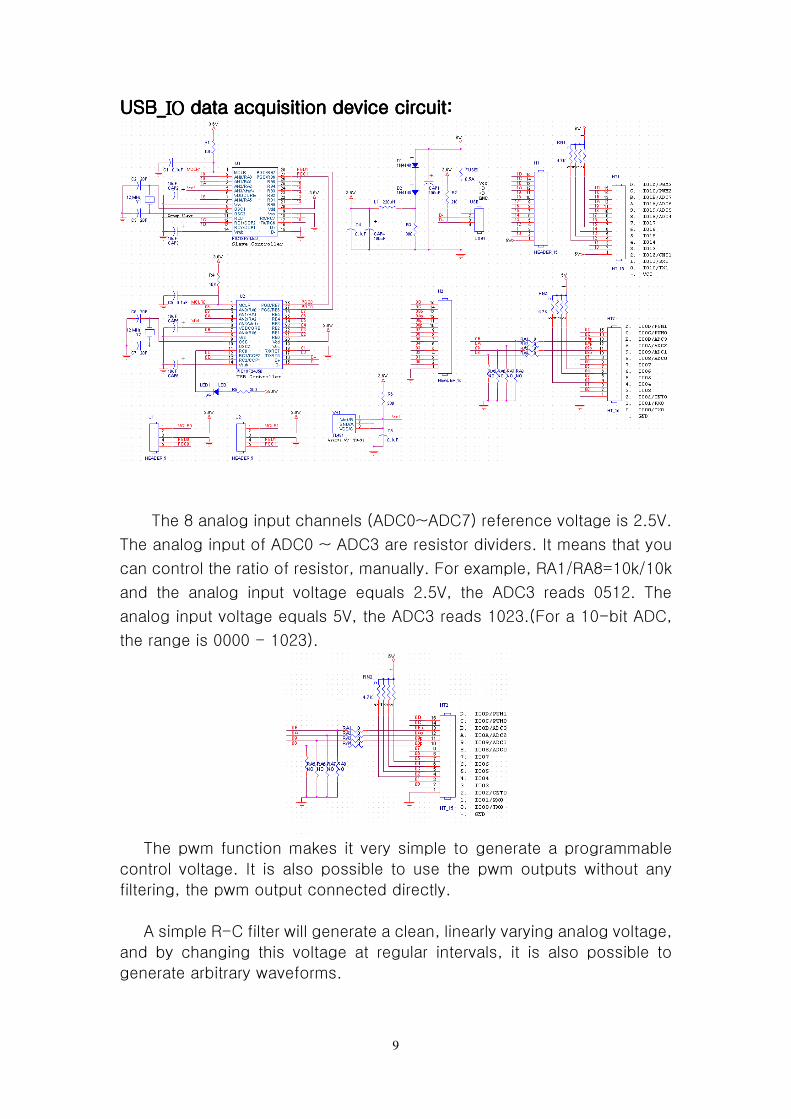
USBUSBUSBUSB_IO_IO_IO_IO data acquisition data acquisition data acquisition data acquisition devicedevicedevicedevice circuit circuit circuit circuit::::
The 8 analog input channels (ADC0~ADC7) reference voltage is 2.5V.
The analog input of ADC0 ~ ADC3 are resistor dividers. It means that you
can control the ratio of resistor, manually. For example, RA1/RA8=10k/10k
and the analog input voltage equals 2.5V, the ADC3 reads 0512. The
analog input voltage equals 5V, the ADC3 reads 1023.(For a 10-bit ADC,
the range is 0000 - 1023).
The pwm function makes it very simple to generate a programmable
control voltage. It is also possible to use the pwm outputs without any
filtering, the pwm output connected directly.
A simple R-C filter will generate a clean, linearly varying analog voltage,
and by changing this voltage at regular intervals, it is also possible to
generate arbitrary waveforms.

10
USB data acquisition USB data acquisition USB data acquisition USB data acquisition devicedevicedevicedevice PCBPCBPCBPCB::::
USB data USB data USB data USB data acquisition acquisition acquisition acquisition devicedevicedevicedevice outlineoutlineoutlineoutline::::

11
USB data acquisition USB data acquisition USB data acquisition USB data acquisition devicedevicedevicedevice the parts list the parts list the parts list the parts list::::
Name Spec. Note Entity picture
1 CAP1,CAP4 100uF Capacity
(Attention polarity)
2 CAP2,CAP3,
CAP5,CAP6
10uF Capacity
(Attention polarity)
3 C1,C4,C5,C8 0.1uF Capacity
4 C2,C3,C6,C7 20P Capacity
5 D1,D2 1N4148 Diode
(Attention polarity)
6 FUSE1 0.5A Polymer Resettable Fuse
7 H2,H1 HEADER 15 None
8 J1,J2 HEADER 5 None 9 HT2,HT1 Terminal Block
Connector
10 LED1 LED DIP LED 3mm
(Attention polarity)
11 L1 220uH DIP inductance
12 RN1,RN2 4.7K ohm DIP 5P4R resistance
(Attention Pin 1)
13 USB1 USB Mini USB Connector
14 U1,U2 PIC18F24J50 USB Controller
15 R4,R1 10K ohm 1/8W resistance
16 R3,R5,R6 300 ohm 1/8W resistance
17 R2 2K ohm 1/8W resistance

12
18 RA5,RA6,
RA7,RA8
None
19 RA1,RA2,
RA3,RA4
0 ohm 1/4W resistance
20 Y1,Y2 12 MHz Quartz crystal
21 VR1 TL431(LM431) Voltage Reference
22 USB Line Mini USB Line
23 PCB PCB

13
Steps for installation the components of Steps for installation the components of Steps for installation the components of Steps for installation the components of USB data USB data USB data USB data
acquisition acquisition acquisition acquisition devicedevicedevicedevice::::
1. Assemble the USB connector and micro-controller U1 and U2.
2. Assemble resistance R1,R4(the 10K ohm), RA1,RA2,RA3,RA4(the 0
ohms), R2(the 2K ohm), R3,R5,R6(the 300 ohm).
3. Assemble resistance RN1,RN2 (the 4.7K ohm, attention installs Pin 1).

14
4. Assemble quartz crystal Y1,Y2(12MHz), C2, C3, C6,C7 (capacity 20pF).
5. Assemble D1 and D2(the 1N4148 diode, attention polarity) and
inductance L1(220uH).
6. Assemble LED1 (LED, attention polarity). polymer resettable fuse
FUSE1(0.5A) and VR1(TL431).

15
7. Assemble capacity CAP1, CAP4 (100uF, attention polarity), CAP2,
CAP3, CAP5, CAP6 (10uF, attention polarity), C1, C5, C8(0.1uF), and
Terminal Block Connector.

16
Visual Basic 6.0 Test ProgramVisual Basic 6.0 Test ProgramVisual Basic 6.0 Test ProgramVisual Basic 6.0 Test Program::::