usb floppy disk controller - keil floppy disk controller features 3.3 volt, ... pin should be tied...
TRANSCRIPT
SMSC DS – USB97CFDC2-01 Rev. 12/13/2001
DATASHEET
USB97CFDC2-01 ADVANCE INFORMATION
USB Floppy Disk Controller
FEATURES 3.3 Volt, Low Power Operation
Complete USB Specification 1.1 Compatibility
- Includes USB Transceiver - Based on an Enhanced Version of SMSC’s
Industry Proven USB97C100 USB Controller
Complete System Solution Including USB Mass Storage Class Compliant Win98/2000 Driver and Firmware
- Supports 640K, 720K, 1.44M, 1.2M Windows 98 J, and 1.2M NEC DOS 6.x Formats
- Supports Both the UFI and SFF8070i Command Sets
- Supports USB Mass Storage Compliant Bootable Floppy BIOS
- 4ms Seek Times - USB 1.1 Compliance, Including Low Power
Device Class SUSPEND Mode Operation and Power Control of Disk Drive
- Disk Drive Feedback of Readiness Upon Power Re-Application Option
- Option for Ultra High Performance Using Additional Caching SRAM
- Support for Floppy Drive Power Control
Contains SMSC’s Industry Proven Floppy Disk Controller
- Licensed CMOS 765B Floppy Disk Controller - Supports Single Normal or Three Mode Floppy
Drives - Supports Vertical Recording Format and High
Capacity Drives in User Written Firmware Applications
- Detects All Overrun and Underrun Conditions - Sophisticated Power Control Circuitry (PCC)
Including Multiple Powerdown Modes for Reduced Power Consumption
Enhanced Digital Data Separator
- 1 Mbps, 500 Kbps, 300 Kbps, 250 Kbps Data Rates
- Programmable Precompensation Modes
Intelligent Auto Power Management
- <250µA SUSPEND Current - <75mA Operating Current
Integrated 32Kbyte Program ROM - Uses external 3 wire serial EEPROM provides
storage for unique OEM identification and string descriptors and drive option settings.
- 10 options for various drive parameters are externally selectable via serial EEPROM data.
Optional External Program Memory Interface for
Custom Applications
- 32K Byte Code Space - Flash, SRAM, or EPROM Memory
4KB Internal Buffer SRAM for High Performance Operation
Integrated 14.318 MHz Crystal Driver Circuit
100 pin TQFP package (12.0 x 12.0 mm body)
- 25% smaller body size than other 100 pin TQFP packages
ORDERING INFORMATION
Order Number: USB97CFDC2-MN-01X 100 Pin TQFP Package

SMSC DS – USB97CFDC2-01 Page 2 Rev. 12/13/2001
DATASHEET
80 Arkay Drive Hauppauge, NY 11788 (631) 435-6000 FAX (631) 273-3123 Copyright © SMSC 2004. All rights reserved. Circuit diagrams and other information relating to SMSC products are included as a means of illustrating typical applications. Consequently, complete information sufficient for construction purposes is not necessarily given. Although the information has been checked and is believed to be accurate, no responsibility is assumed for inaccuracies. SMSC reserves the right to make changes to specifications and product descriptions at any time without notice. Contact your local SMSC sales office to obtain the latest specifications before placing your product order. The provision of this information does not convey to the purchaser of the described semiconductor devices any licenses under any patent rights or other intellectual property rights of SMSC or others. All sales are expressly conditional on your agreement to the terms and conditions of the most recently dated version of SMSC's standard Terms of Sale Agreement dated before the date of your order (the "Terms of Sale Agreement"). The product may contain design defects or errors known as anomalies which may cause the product's functions to deviate from published specifications. Anomaly sheets are available upon request. SMSC products are not designed, intended, authorized or warranted for use in any life support or other application where product failure could cause or contribute to personal injury or severe property damage. Any and all such uses without prior written approval of an Officer of SMSC and further testing and/or modification will be fully at the risk of the customer. Copies of this document or other SMSC literature, as well as the Terms of Sale Agreement, may be obtained by visiting SMSC’s website at http://www.smsc.com. SMSC is a registered trademark of Standard Microsystems Corporation (“SMSC”). Product names and company names are the trademarks of their respective holders.
SMSC DISCLAIMS AND EXCLUDES ANY AND ALL WARRANTIES, INCLUDING WITHOUT LIMITATION ANY AND ALL IMPLIED WARRANTIES OF MERCHANTABILITY, FITNESS FOR A PARTICULAR PURPOSE, TITLE, AND AGAINST INFRINGEMENT AND THE LIKE, AND ANY AND ALL WARRANTIES ARISING FROM ANY COURSE OF DEALING OR USAGE OF TRADE. IN NO EVENT SHALL SMSC BE LIABLE FOR ANY DIRECT, INCIDENTAL, INDIRECT, SPECIAL, PUNITIVE, OR CONSEQUENTIAL DAMAGES; OR FOR LOST DATA, PROFITS, SAVINGS OR REVENUES OF ANY KIND; REGARDLESS OF THE FORM OF ACTION, WHETHER BASED ON CONTRACT; TORT; NEGLIGENCE OF SMSC OR OTHERS; STRICT LIABILITY; BREACH OF WARRANTY; OR OTHERWISE; WHETHER OR NOT ANY REMEDY OF BUYER IS HELD TO HAVE FAILED OF ITS ESSENTIAL PURPOSE, AND WHETHER OR NOT SMSC HAS BEEN ADVISED OF THE POSSIBILITY OF SUCH DAMAGES.
SMSC DS – USB97CFDC2-01 Page 3 Rev. 12/13/2001
DATASHEET
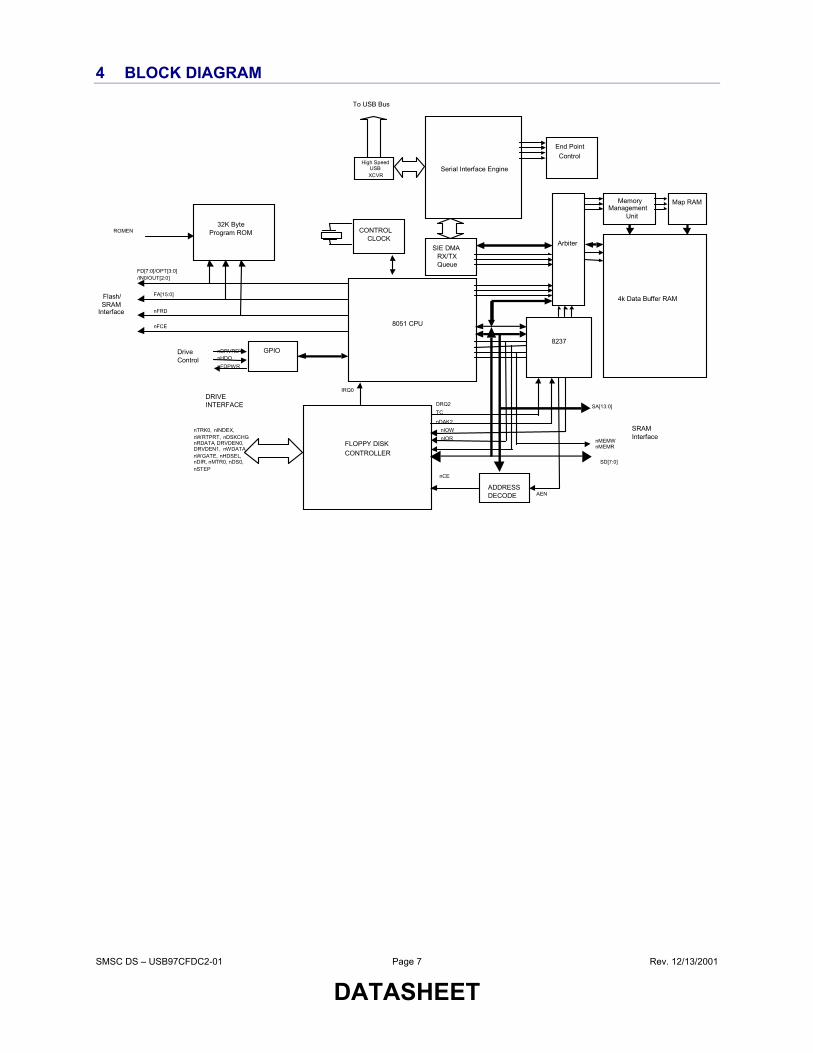
1 GENERAL DESCRIPTION The USB97CFDC2-01 is an integration of an Enhanced Multi-Endpoint USB 1.1 Peripheral Controller, a 32K Byte Program ROM, and the SMSC Floppy Disk Controller used in many of its Super IO products, such as the FDC37C869. Special care in the design has been taken to assure the lowest possible system current draw (<250µA) during SUSPEND mode operation. Provisions for external program Flash Memory up to 32K bytes for program storage is provided for customized applications. Several pins are provided for controlling external power control elements and sensing specialized drive functions. Individual manufacturers may provide their unique USB vendor and product IDs and descriptor strings via an external 3 wire serial EEPROM. Up to 16 different configuration options for various drive related parameters are provided by 4 external configuration input pins which can be read at power-on reset.

SMSC DS – USB97CFDC2-01 Page 4 Rev. 12/13/2001
DATASHEET
TABLE OF CONTENTS
1 GENERAL DESCRIPTION .............................................................................................................................3
2 DESCRIPTION OF PIN FUNCTIONS...........................................................................................................5
3 PIN CONFIGURATION...................................................................................................................................6
4 BLOCK DIAGRAM ..........................................................................................................................................7
5 PIN DESCRIPTIONS........................................................................................................................................8 5.1 BUFFER TYPE DESCRIPTIONS ....................................................................................................................11
6 CONFIGURATION OPTIONS......................................................................................................................12
7 BOARD TEST MODE OPERATION ...........................................................................................................14
8 DC PARAMETERS.........................................................................................................................................15
9 AC PARAMETERS.........................................................................................................................................17
10 USB PARAMETERS.......................................................................................................................................19 10.1 USB DC PARAMETERS.........................................................................................................................19 10.2 USB AC PARAMETERS.........................................................................................................................21
11 MECHANICAL OUTLINE............................................................................................................................24
SMSC DS – USB97CFDC2-01 Page 5 Rev. 12/13/2001
DATASHEET
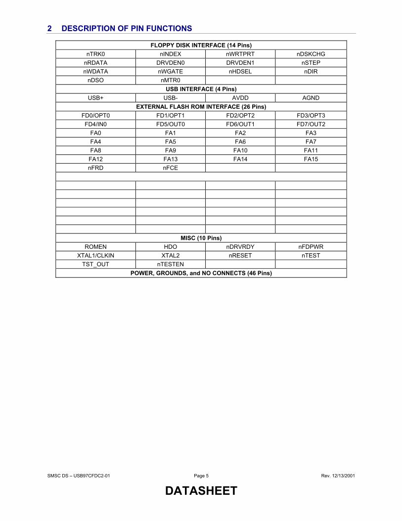
2 DESCRIPTION OF PIN FUNCTIONS
FLOPPY DISK INTERFACE (14 Pins) nTRK0 nINDEX nWRTPRT nDSKCHG
nRDATA DRVDEN0 DRVDEN1 nSTEP nWDATA nWGATE nHDSEL nDIR
nDSO nMTR0 USB INTERFACE (4 Pins)
USB+ USB- AVDD AGND EXTERNAL FLASH ROM INTERFACE (26 Pins)
FD0/OPT0 FD1/OPT1 FD2/OPT2 FD3/OPT3 FD4/IN0 FD5/OUT0 FD6/OUT1 FD7/OUT2
FA0 FA1 FA2 FA3 FA4 FA5 FA6 FA7 FA8 FA9 FA10 FA11
FA12 FA13 FA14 FA15 nFRD nFCE
MISC (10 Pins) ROMEN HDO nDRVRDY nFDPWR
XTAL1/CLKIN XTAL2 nRESET nTEST TST_OUT nTESTEN
POWER, GROUNDS, and NO CONNECTS (46 Pins)
SMSC DS – USB97CFDC2-01 Page 6 Rev. 12/13/2001
DATASHEET
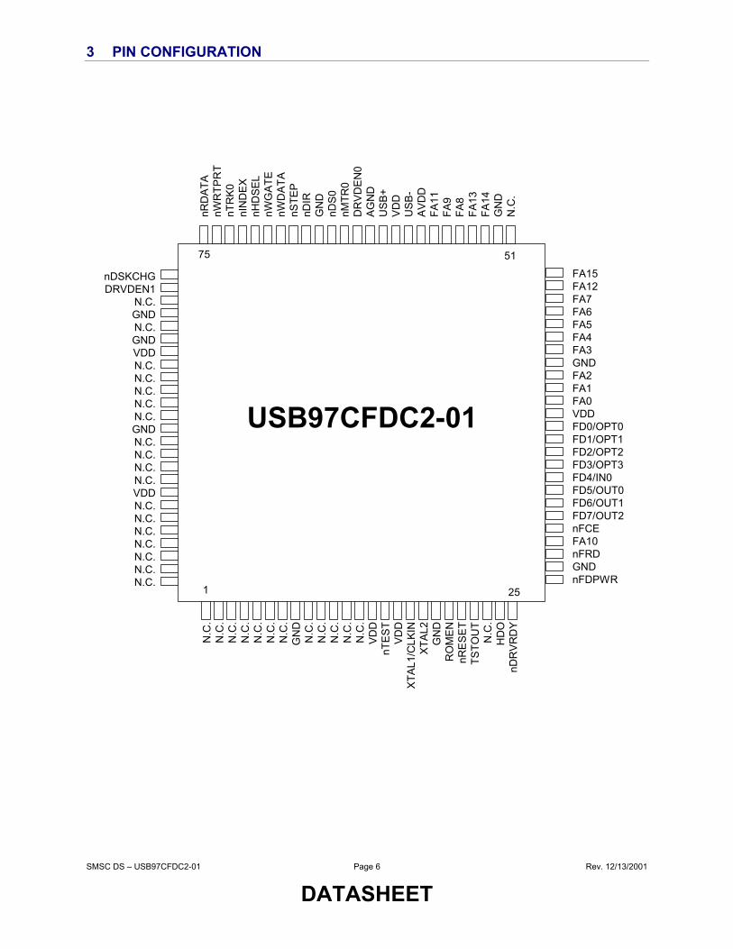
3 PIN CONFIGURATION
N.C
.N
.C.
N.C
.N
.C.
N.C
.N
.C.
N.C
.G
ND
N.C
.N
.C.
N.C
.N
.C.
N.C
.V
DD
nTE
ST
VD
DX
TAL1
/CLK
INX
TAL2
GN
DR
OM
EN
nRE
SE
TTS
TOU
TN
.C.
HD
OnD
RV
RD
Y
USB97CFDC2
1 25
5175
nRD
ATA
nWR
TPR
TnT
RK
0nI
ND
EX
nHD
SE
LnW
GA
TEnW
DA
TAnS
TEP
nDIR
GN
DnD
S0
nMTR
0D
RV
DE
N0
AG
ND
US
B+
VD
DU
SB
-A
VD
DFA
11FA
9FA
8FA
13FA
14G
ND
N.C
.
nDSKCHGDRVDEN1
N.C.GNDN.C.GNDVDDN.C.N.C.N.C.N.C.N.C.GNDN.C.N.C.N.C.N.C.VDDN.C.N.C.N.C.N.C.N.C.N.C.N.C.
FA15FA12FA7FA6FA5FA4FA3GNDFA2FA1FA0VDDFD0/OPT0FD1/OPT1FD2/OPT2FD3/OPT3FD4/IN0FD5/OUT0FD6/OUT1FD7/OUT2nFCEFA10nFRDGNDnFDPWR
USB97CFDC2-01
SMSC DS – USB97CFDC2-01 Page 7 Rev. 12/13/2001
DATASHEET
4 BLOCK DIAGRAM
8051 CPU
8237
4k Data Buffer RAM
MemoryManagement
Unit
Map RAM
ArbiterSIE DMA
RX/TXQueue
End PointControl
Serial Interface Engine
GPIO
FD[7:0]/OPT[3:0]/IN0/OUT[2:0]
nFRD
nFCE
DriveControl
Flash/SRAM
Interface
IRQ0
SD[7:0]
SA[13:0]
nIOWnIOR nMEMW
nMEMR
High SpeedUSBXCVR
To USB Bus
FA[15:0]
FLOPPY DISKCONTROLLER
DRQ2TC
nDAK2
ADDRESSDECODE
nCE
AEN
SRAMInterface
nTRK0, nINDEX,nWRTPRT, nDSKCHGnRDATA, DRVDEN0,DRVDEN1, nWDATA,nWGATE, nHDSEL,nDIR, nMTR0, nDS0,nSTEP
DRIVEINTERFACE
CLOCKCONTROL
nHDOnDRVRDY
nFDPWR
32K ByteProgram ROMROMEN
SMSC DS – USB97CFDC2-01 Page 8 Rev. 12/13/2001
DATASHEET
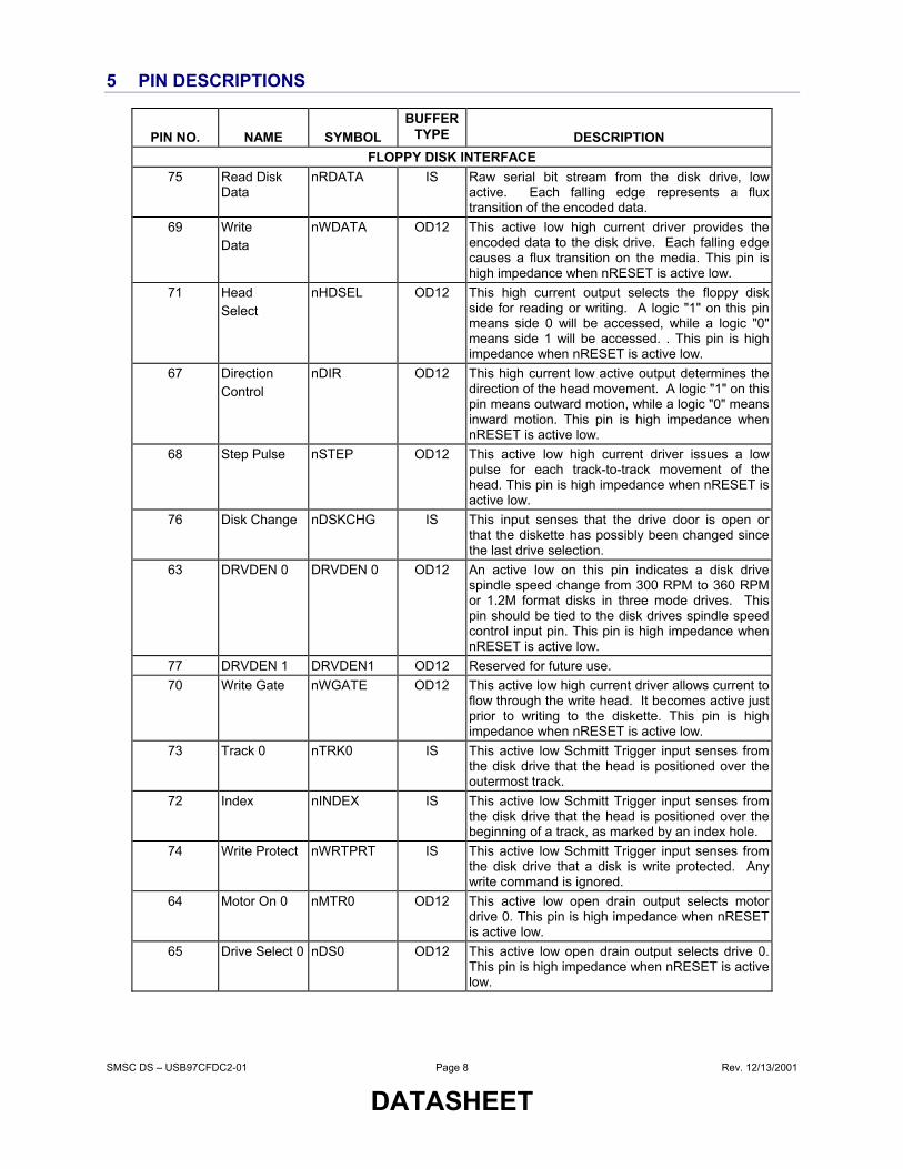
5 PIN DESCRIPTIONS
PIN NO.
NAME
SYMBOL
BUFFER TYPE
DESCRIPTION
FLOPPY DISK INTERFACE 75 Read Disk
Data nRDATA IS Raw serial bit stream from the disk drive, low
active. Each falling edge represents a flux transition of the encoded data.
69 Write Data
nWDATA OD12 This active low high current driver provides the encoded data to the disk drive. Each falling edge causes a flux transition on the media. This pin is high impedance when nRESET is active low.
71 Head Select
nHDSEL OD12 This high current output selects the floppy disk side for reading or writing. A logic "1" on this pin means side 0 will be accessed, while a logic "0" means side 1 will be accessed. . This pin is high impedance when nRESET is active low.
67 Direction Control
nDIR OD12 This high current low active output determines the direction of the head movement. A logic "1" on this pin means outward motion, while a logic "0" means inward motion. This pin is high impedance when nRESET is active low.
68 Step Pulse nSTEP OD12 This active low high current driver issues a low pulse for each track-to-track movement of the head. This pin is high impedance when nRESET is active low.
76 Disk Change nDSKCHG IS This input senses that the drive door is open or that the diskette has possibly been changed since the last drive selection.
63 DRVDEN 0 DRVDEN 0 OD12 An active low on this pin indicates a disk drive spindle speed change from 300 RPM to 360 RPM or 1.2M format disks in three mode drives. This pin should be tied to the disk drives spindle speed control input pin. This pin is high impedance when nRESET is active low.
77 DRVDEN 1 DRVDEN1 OD12 Reserved for future use. 70 Write Gate nWGATE OD12 This active low high current driver allows current to
flow through the write head. It becomes active just prior to writing to the diskette. This pin is high impedance when nRESET is active low.
73 Track 0 nTRK0 IS This active low Schmitt Trigger input senses from the disk drive that the head is positioned over the outermost track.
72 Index nINDEX IS This active low Schmitt Trigger input senses from the disk drive that the head is positioned over the beginning of a track, as marked by an index hole.
74 Write Protect nWRTPRT IS This active low Schmitt Trigger input senses from the disk drive that a disk is write protected. Any write command is ignored.
64 Motor On 0 nMTR0 OD12 This active low open drain output selects motor drive 0. This pin is high impedance when nRESET is active low.
65 Drive Select 0 nDS0 OD12 This active low open drain output selects drive 0. This pin is high impedance when nRESET is active low.

SMSC DS – USB97CFDC2-01 Page 9 Rev. 12/13/2001
DATASHEET
PIN NO.
NAME
SYMBOL
BUFFER TYPE
DESCRIPTION
USB INTERFACE 59 61
USB Bus Data
USB- USB+
IO-U These pins connect to the USB data signals through 33 ohm series resistors. The USB+ line should be pulled up with a 5%, 1.5K ohm resistor to indicate that this is a high speed USB device.
58 USB Transceiver Supply
AVDD This is the 3.3V supply to the internal USB transceiver.
62 USB Transceiver Ground
AGND This is the supply ground for the internal USB transceiver.
PROGRAM MEMORY INTERFACE 38-35 Program
Memory Data Bus/Option Select
FD[3:0]/ OPT[3:0]
IO8 These signals are used to transfer data between the internal 8051 and the external program memory when operating in external program memory mode (See ROMEN pin). When operating from internal program memory, the OPT3 pin must be tied high thru a resistor and the OPT[2:0] pins tied low thru a resistor (See configuration description section). These pins are not driven while the USB97CFDC2-01 is in SUSPEND mode and internal ROM mode is active. They are driven while in SUSPEND in external ROM mode..
34 Program Memory Data Bus/EEPROM Input
FD4/IN0 IO8 This signal is used to transfer data between the internal 8051 and the external program memory when operating in external program memory mode (See ROMEN pin). When operating from internal program memory, this pin is the input data from an external serial EEPROM that contains manufacturer specific ID and string information, as required by the USB specification, and drive options. This pin is not driven while the USB97CFDC2-01 is in SUSPEND mode and internal ROM mode is active. It is driven while in SUSPEND in external ROM mode...
33-31 Program Memory Data Bus/EEPROM Output
FD[7:5]/ OUT[2:0]
IO8 This signal is used to transfer data between the internal 8051 and the external program memory when operating in external program memory mode (See ROMEN pin). When operating from internal program memory, these pins are the output data and strobes to an external serial EEPROM that contains manufacturer specific ID and string information, as required by the USB specification, and drive options. These pins are driven while the USB97CFDC2-01 is in SUSPEND mode.
50, 53, 54, 49, 57, 29, 56, 55, 48-44, 42-40,
Flash Memory Address Bus
FA[15:0] O8 These signals address memory locations within the FLASH memory.
28 Flash Memory Read Strobe
nFRD O8 Flash ROM Read; active low
30 Flash Memory Chip Select
nFCE O8 Flash ROM Chip Select; active low
MISCELLANEOUS 17 Crystal
Input/External Clock Input
XTAL1/ CLKIN
ICLKx 14.318Mhz Crystal or clock input. This pin can be connected to one terminal of the crystal or can be connected to an external 14.318Mhz clock when a crystal is not used.

SMSC DS – USB97CFDC2-01 Page 10 Rev. 12/13/2001
DATASHEET
PIN NO.
NAME
SYMBOL
BUFFER TYPE
DESCRIPTION
18 Crystal Output XTAL2 OCLKx 14.318Mhz Crystal This is the other terminal of the crystal, or left open when an external clock source is used to drive XTAL1/CLKIN. It may not be used to drive any external circuitry other than the crystal circuit.
20 ROM Enable ROMEN IP If this input is tied high or left open, the internal program ROM is enabled. If tied low, external program memory can be used for custom applications.
24 Drive Density Output
HDO I In some configurations of the USB97CFDC, this drive pin indicates if a 640/720K disk is inserted in the drive. Polarity of this signal is determined by the configuration selected by the OPT[3:0] pins at reset. If this pin is not driven by the drive, it should be tied low.
25 Drive Ready nDRVRDY I An active low signal on this pin from the floppy disk drive, after DS0 goes active, indicates that the system may activate MTR0. If the drive does not supply this signal, this pin should be tied low.
26 Drive Power nFDPWR OD24 This active low signal is intended to activate an external power switch, either in the drive or on the system board, to supply power to the floppy disk drive. It is active whenever the USB97CFDC2-01 is not in SUSPEND mode.
21 RESET input nRESET IS This active low signal is used by the system to reset the chip. The active low pulse should be at least 100ns wide.
22 Test output TSTOUT O8 This signal is used for testing the chip via an internal XNOR chain. User should normally leave it unconnected.
15 Test input nTEST I This signal is a manufacturing test pin. It should be tied to VDD for normal operation.
16 Test Enable nTESTEN I This active low signal places the device into board test mode using the XNOR chain. For normal operation this pin should be tied high. See Board Test Mode Operation on page 14
POWER, GROUND, AND NO CONNECTS 14, 39, 60,
82, 93 VDD +3.3V power
8, 19, 27, 43, 52, 66, 79,
81, 88
GND Ground Reference
1-7, 9-13, 23, 51, 78, 80, 83-87, 89-92, 94-100
NC No Connect. These pins should not be connected externally.

SMSC DS – USB97CFDC2-01 Page 11 Rev. 12/13/2001
DATASHEET
5.1 Buffer Type Descriptions
Table 1 - USB97CFDC2-01 Buffer Type Descriptions BUFFER DESCRIPTION
I Input IP Input with 30uA pull-up IS Input with Schmitt trigger O8 Output with 8mA drive IO8 Input/output with 8mA drive
IO8P Input/output with 8mA drive and 30uA pull-up
OD12 Open drain….12mA sink O24 Output with 24mA drive
OD24 Open drain….24mA sink ICLKx XTAL clock input OCLKx XTAL clock output I/O-U See Table 6.
SMSC DS – USB97CFDC2-01 Page 12 Rev. 12/13/2001
DATASHEET
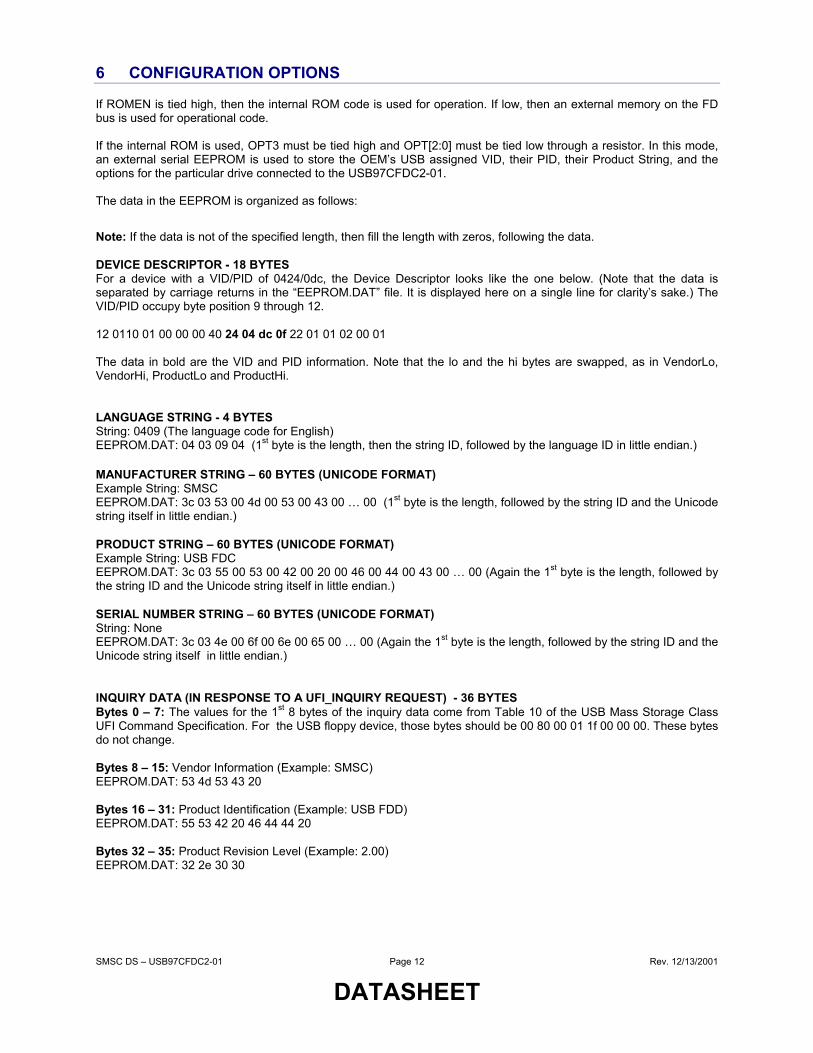
6 CONFIGURATION OPTIONS If ROMEN is tied high, then the internal ROM code is used for operation. If low, then an external memory on the FD bus is used for operational code. If the internal ROM is used, OPT3 must be tied high and OPT[2:0] must be tied low through a resistor. In this mode, an external serial EEPROM is used to store the OEM’s USB assigned VID, their PID, their Product String, and the options for the particular drive connected to the USB97CFDC2-01. The data in the EEPROM is organized as follows:
Note: If the data is not of the specified length, then fill the length with zeros, following the data. DEVICE DESCRIPTOR - 18 BYTES For a device with a VID/PID of 0424/0dc, the Device Descriptor looks like the one below. (Note that the data is separated by carriage returns in the “EEPROM.DAT” file. It is displayed here on a single line for clarity’s sake.) The VID/PID occupy byte position 9 through 12. 12 0110 01 00 00 00 40 24 04 dc 0f 22 01 01 02 00 01 The data in bold are the VID and PID information. Note that the lo and the hi bytes are swapped, as in VendorLo, VendorHi, ProductLo and ProductHi. LANGUAGE STRING - 4 BYTES String: 0409 (The language code for English) EEPROM.DAT: 04 03 09 04 (1st byte is the length, then the string ID, followed by the language ID in little endian.) MANUFACTURER STRING – 60 BYTES (UNICODE FORMAT) Example String: SMSC EEPROM.DAT: 3c 03 53 00 4d 00 53 00 43 00 … 00 (1st byte is the length, followed by the string ID and the Unicode string itself in little endian.) PRODUCT STRING – 60 BYTES (UNICODE FORMAT) Example String: USB FDC EEPROM.DAT: 3c 03 55 00 53 00 42 00 20 00 46 00 44 00 43 00 … 00 (Again the 1st byte is the length, followed by the string ID and the Unicode string itself in little endian.) SERIAL NUMBER STRING – 60 BYTES (UNICODE FORMAT) String: None EEPROM.DAT: 3c 03 4e 00 6f 00 6e 00 65 00 … 00 (Again the 1st byte is the length, followed by the string ID and the Unicode string itself in little endian.) INQUIRY DATA (IN RESPONSE TO A UFI_INQUIRY REQUEST) - 36 BYTES Bytes 0 – 7: The values for the 1st 8 bytes of the inquiry data come from Table 10 of the USB Mass Storage Class UFI Command Specification. For the USB floppy device, those bytes should be 00 80 00 01 1f 00 00 00. These bytes do not change. Bytes 8 – 15: Vendor Information (Example: SMSC) EEPROM.DAT: 53 4d 53 43 20 Bytes 16 – 31: Product Identification (Example: USB FDD) EEPROM.DAT: 55 53 42 20 46 44 44 20 Bytes 32 – 35: Product Revision Level (Example: 2.00) EEPROM.DAT: 32 2e 30 30
SMSC DS – USB97CFDC2-01 Page 13 Rev. 12/13/2001
DATASHEET
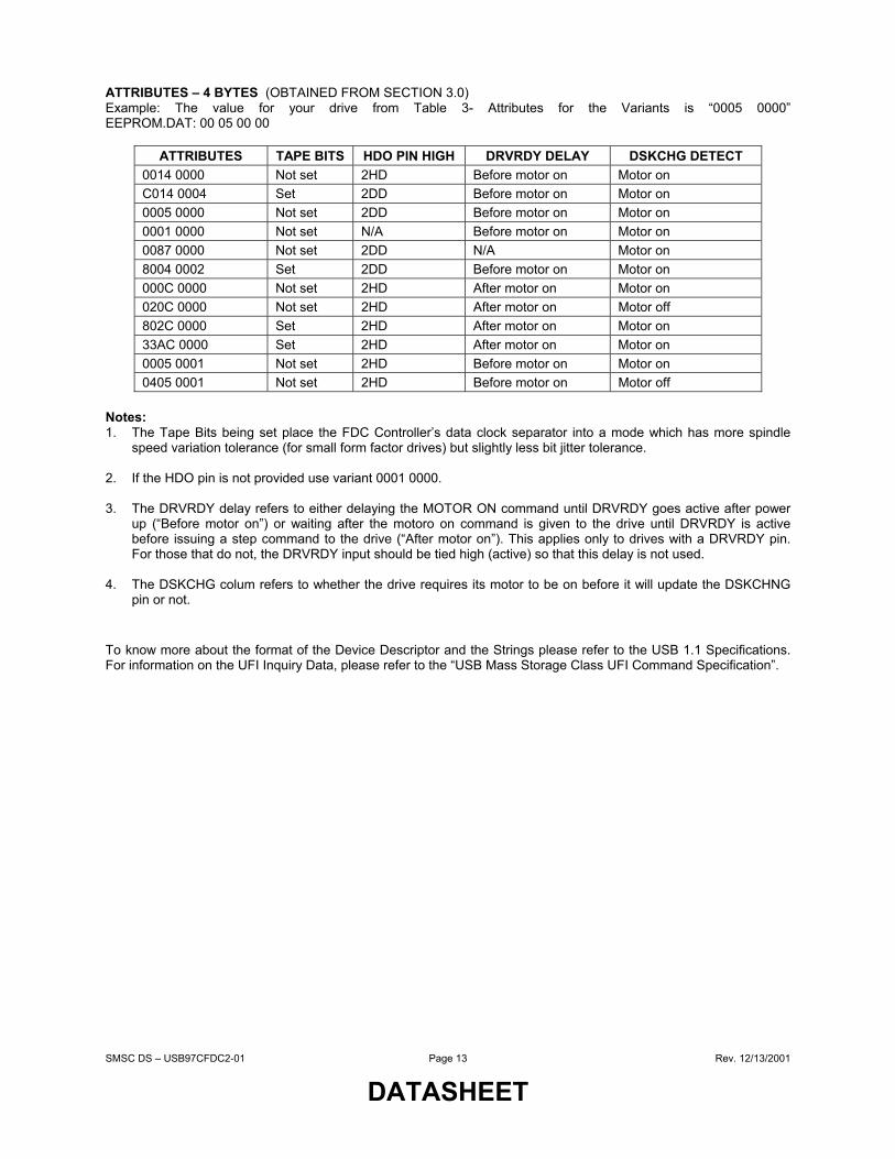
ATTRIBUTES – 4 BYTES (OBTAINED FROM SECTION 3.0) Example: The value for your drive from Table 3- Attributes for the Variants is “0005 0000” EEPROM.DAT: 00 05 00 00
ATTRIBUTES TAPE BITS HDO PIN HIGH DRVRDY DELAY DSKCHG DETECT 0014 0000 Not set 2HD Before motor on Motor on C014 0004 Set 2DD Before motor on Motor on 0005 0000 Not set 2DD Before motor on Motor on 0001 0000 Not set N/A Before motor on Motor on 0087 0000 Not set 2DD N/A Motor on 8004 0002 Set 2DD Before motor on Motor on 000C 0000 Not set 2HD After motor on Motor on 020C 0000 Not set 2HD After motor on Motor off 802C 0000 Set 2HD After motor on Motor on 33AC 0000 Set 2HD After motor on Motor on 0005 0001 Not set 2HD Before motor on Motor on 0405 0001 Not set 2HD Before motor on Motor off
Notes: 1. The Tape Bits being set place the FDC Controller’s data clock separator into a mode which has more spindle
speed variation tolerance (for small form factor drives) but slightly less bit jitter tolerance. 2. If the HDO pin is not provided use variant 0001 0000. 3. The DRVRDY delay refers to either delaying the MOTOR ON command until DRVRDY goes active after power
up (“Before motor on”) or waiting after the motoro on command is given to the drive until DRVRDY is active before issuing a step command to the drive (“After motor on”). This applies only to drives with a DRVRDY pin. For those that do not, the DRVRDY input should be tied high (active) so that this delay is not used.
4. The DSKCHG colum refers to whether the drive requires its motor to be on before it will update the DSKCHNG
pin or not.
To know more about the format of the Device Descriptor and the Strings please refer to the USB 1.1 Specifications. For information on the UFI Inquiry Data, please refer to the “USB Mass Storage Class UFI Command Specification”.
SMSC DS – USB97CFDC2-01 Page 14 Rev. 12/13/2001
DATASHEET
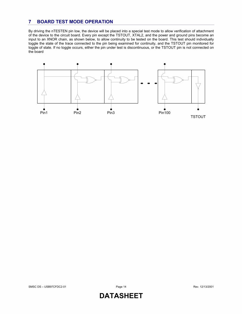
7 BOARD TEST MODE OPERATION By driving the nTESTEN pin low, the device will be placed into a special test mode to allow verification of attachment of the device to the circuit board. Every pin except the TSTOUT, XTAL2, and the power and ground pins become an input to an XNOR chain, as shown below, to allow continuity to be tested on the board. This test should individually toggle the state of the trace connected to the pin being examined for continuity, and the TSTOUT pin monitored for toggle of state. If no toggle occurs, either the pin under test is discontinuous, or the TSTOUT pin is not connected on the board
Pin1 Pin2 Pin3 Pin100TSTOUT

SMSC DS – USB97CFDC2-01 Page 15 Rev. 12/13/2001
DATASHEET
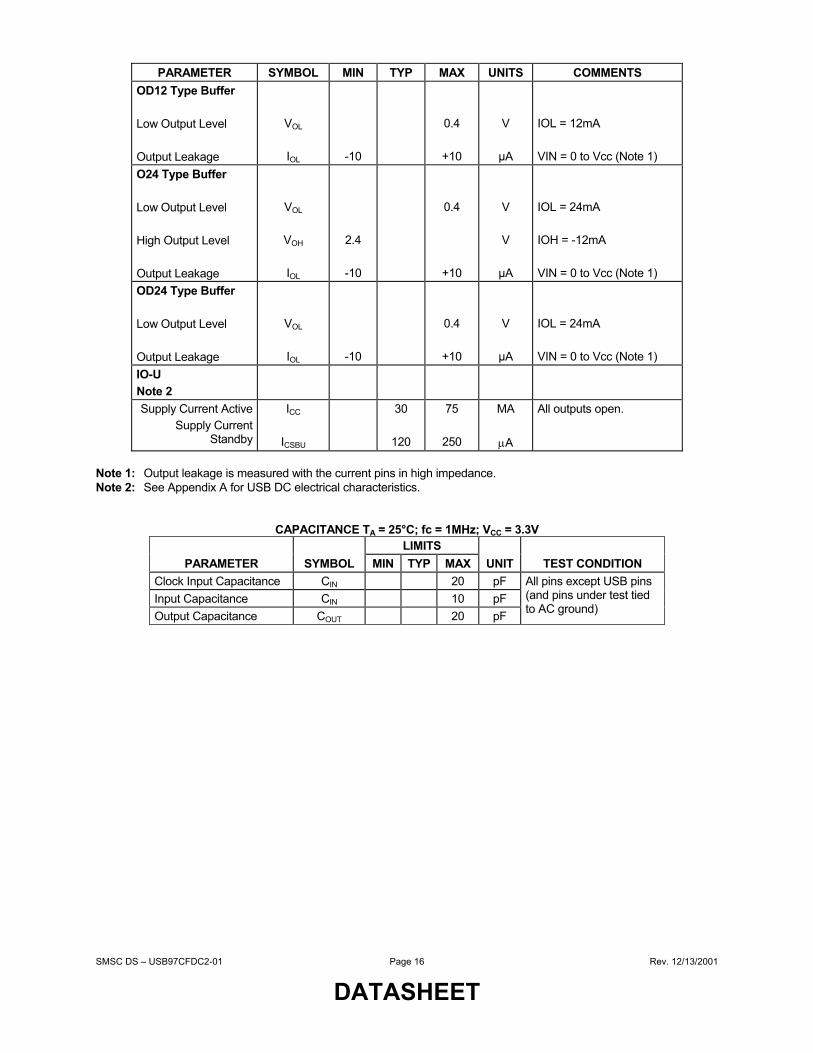
8 DC PARAMETERS MAXIMUM GUARANTEED RATINGS Operating Temperature Range........................................................................................................................... 0oC to +70oC Storage Temperature Range ............................................................................................................................-55o to +150oC Lead Temperature Range (soldering, 10 seconds) ..................................................................................................... +325oC Positive Voltage on any pin, with respect to Ground (Note 1) ...................................................................................Vcc+0.3V Negative Voltage on any pin, with respect to Ground......................................................................................................-0.3V Maximum Vcc...................................................................................................................................................................+3.6V Note 1: Maximum voltage on all I type Inputs and the IS inputs, OD12 and OD24 outputs for floppy disk drive interface is 5.25V *Stresses above the specified parameters could cause permanent damage to the device. This is a stress rating only and functional operation of the device at any other condition above those indicated in the operation sections of this specification is not implied. Note 2: When powering this device from laboratory or system power supplies, it is important that the Absolute Maximum Ratings not be exceeded or device failure can result. Some power supplies exhibit voltage spikes on their outputs when the AC power is switched on or off. In addition, voltage transients on the AC power line may appear on the DC output. When this possibility exists, it is suggested that a clamp circuit be used.
DC ELECTRICAL CHARACTERISTICS (TA = 0°C - 70°C, Vcc = +3.3 V ± 10%)
PARAMETER SYMBOL MIN TYP MAX UNITS COMMENTS I Type Input Buffer Low Input Level High Input Level
VILI
VIHI
2.0
0.8
V
V
TTL Levels
ICLK Input Buffer Low Input Level High Input Level
VILCK
VIHCK
2.2
0.4
V
V
Input Leakage (All I and IS buffers) Low Input Leakage High Input Leakage
IIL
IIH
-10
-10
+10
+10
uA
uA
VIN = 0 VIN = VCC
O8 Type Buffer Low Output Level High Output Level Output Leakage
VOL
VOH
IOL
2.4
-10
0.4
+10
V
V
UA
IOL = 8 mA IOH = -4 mA VIN = 0 to VCC (Note 1)
I/O8(P) Type Buffer Low Output Level High Output Level Output Leakage IO8
IO8P
VOL
VOH
IOL
IOL
2.4
-10 -50
0.4
+10 +10
V
V
µA µA
IOL = 8mA IOH = -4mA VIN = 0 to Vcc (Note 1) VIN = 0 to Vcc (Note 1)
SMSC DS – USB97CFDC2-01 Page 16 Rev. 12/13/2001
DATASHEET
PARAMETER SYMBOL MIN TYP MAX UNITS COMMENTS OD12 Type Buffer Low Output Level Output Leakage
VOL
IOL
-10
0.4
+10
V
µA
IOL = 12mA VIN = 0 to Vcc (Note 1)
O24 Type Buffer Low Output Level High Output Level Output Leakage
VOL
VOH
IOL
2.4
-10
0.4
+10
V
V
µA
IOL = 24mA IOH = -12mA VIN = 0 to Vcc (Note 1)
OD24 Type Buffer Low Output Level Output Leakage
VOL
IOL
-10
0.4
+10
V
µA
IOL = 24mA VIN = 0 to Vcc (Note 1)
IO-U Note 2
Supply Current Active Supply Current
Standby
ICC
ICSBU
30
120
75
250
MA
µA
All outputs open.
Note 1: Output leakage is measured with the current pins in high impedance. Note 2: See Appendix A for USB DC electrical characteristics.
CAPACITANCE TA = 25°C; fc = 1MHz; VCC = 3.3V LIMITS
PARAMETER SYMBOL MIN TYP MAX UNIT TEST CONDITION Clock Input Capacitance CIN 20 pF Input Capacitance CIN 10 pF Output Capacitance COUT 20 pF
All pins except USB pins (and pins under test tied to AC ground)
SMSC DS – USB97CFDC2-01 Page 17 Rev. 12/13/2001
DATASHEET
9 AC PARAMETERS
t2t1
t2CLOCKI
FIGURE 1 - INPUT CLOCK TIMING
Table 2 – Input Clock Timing Parameters NAME DESCRIPTION MIN TYP MAX UNITS
t1 Clock Cycle Time for 14.318MHz 69.84 ns t2 Clock High Time/Low Time for 24MHz 41.9/
27.9 27.9/
41.9 ns
tr, tf Clock Rise Time/Fall Time (not shown) 5 ns
FA[0:19]
FD[7:0
nFRD
nFW R
t1 t5
t3 t4
t2
FIGURE 2 – FLASH READ TIMING
Table 3 – Flash Read Timing
NAME PARAMETER MIN TYP MAX UNITS t1 FA[14:0] Address setup time to nFRD asserted 40 ns t2 nFRD pulse width 110 ns t3 FD[7:0] Data setup time to nFRD de-asserted 30 ns t4 FD[7:0] Data hold time from nFRD de-asserted 0 ns t5 FA[14:0] Address hold time from nFRD de-asserted 35 ns
SMSC DS – USB97CFDC2-01 Page 18 Rev. 12/13/2001
DATASHEET
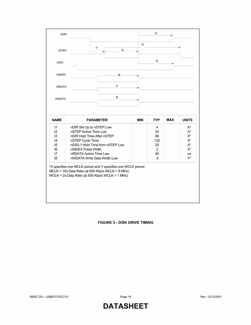
FIGURE 3 - DISK DRIVE TIMING
TYP
t3
t1t2
t4
t5
t6
t7
t8
nDIR
nSTEP
nDS0
nINDEX
nRDATA
nWDATA
*X specifies one MCLK period and Y specifies one WCLK period.MCLK = 16x Data Rate (at 500 Kbp/s MCLK = 8 MHz)WCLK = 2x Data Rate (at 500 Kbp/s WCLK = 1 MHz)
PARAMETER MIN MAX UNITS
t1t2t3t4t5t6t7t8
nDIR Set Up to nSTEP LownSTEP Active Time LownDIR Hold Time After nSTEPnSTEP Cycle TimenDS0-1 Hold Time from nSTEP LownINDEX Pulse WidthnRDATA Active Time LownWDATA Write Data Width Low
X*X*X*X*X*X*nsY*
42496
132202
40.5
NAME
SMSC DS – USB97CFDC2-01 Page 19 Rev. 12/13/2001
DATASHEET
10 USB PARAMETERS The following tables and diagrams were obtained from the USB specification
10.1 USB DC PARAMETERS
0.0
0.2
0.4
0.6
0.8
1.0
0.0 0.2 0.4 0.6 0.8 1.0 1.2 1.4 1.6 1.8 2.0 2.2 2.4 2.6 2.8 3.0 3.2Common Mode Input Voltage (volts)
Min
imum
Diff
eren
tial S
ensi
tivity
(vol
ts)
FIGURE 4 - DIFFERENTIAL INPUT SENSITIVITY OVER ENTIRE COMMON MODE RANGE
Table 4 - DC Electrical Characteristics
PARAMETER
SYMBOL CONDITIONS (NOTE 1, 2)
MIN
TYP
MAX
UNIT
Supply Voltage Powered (Host or Hub) Port VBUS 4.4 5.25 V Supply Current Function ICC Note 4 100 mA Un-configured Function (in) ICCINIT Note 5 100 uA Suspend Device ICCS 100 uA Leakage Current Hi-Z State Data Line Leakage
ILO 0 V < VIN < 3.3 V
-10 10 uA
Input Levels Differential Input Sensitivity VDI |(D+) - (D-)|, and
FIGURE 4 0.2 V
Differential Common Mode Range
VCM Includes VDI range
0.8 2.5 V
Single Ended Receiver Threshold
VSE 0.8 2.0 V
Output Levels Static Output Low VOL RL of 1.5 KΩ to
3.6 V 0.3 (3) V
Static Output High VOH RL of 15 KΩ to GND
2.8 3.6 (3) V
Capacitance Transceiver Capacitance CIN Pin to GND 20 pF Terminals Bus Pull-up Resistor on Root Port
RPU (1.5 KΩ +/- 5%) 1.425 1.575 kΩ

SMSC DS – USB97CFDC2-01 Page 20 Rev. 12/13/2001
DATASHEET
PARAMETER
SYMBOL
CONDITIONS (NOTE 1, 2)
MIN
TYP
MAX
UNIT
Bus Pull-down Resistor on Downstream Port
RPD (15 KΩ +/- 5%) 14.25 15.75 kΩ
Note 1: All voltages are measured from the local ground potential, unless otherwise specified. Note 2: All timing use a capacitive load (CL) to ground of 50pF, unless otherwise specified. Note 3: This is relative to VUSBIN. Note 4: This is dependent on block configuration set by software. Note 5: When the internal ring oscillator and waiting for first setup packet.

SMSC DS – USB97CFDC2-01 Page 21 Rev. 12/13/2001
DATASHEET
10.2 USB AC PARAMETERS
Full Speed: 4 to 20ns at CL = 50pF
DifferentialData Lines
10%
Rise Time
90%
Fall Time
tFtR
10%
90%CL
CL
FIGURE 5 - DATA SIGNAL RISE AND FALL TIME
TPERIOD
DifferentialData Lines
CrossoverPoints
PairedTransitions
N * TPERIOD + TxJR2
ConsecutiveTransitions
N * TPERIOD + TxJR1
FIGURE 6 - DIFFERENTIAL DATA JITTER
TPERIOD
DifferentialData Lines
CrossoverPoint
CrossoverPoint Extended
Source EOP Width: TEOPT
Receiver EOP Width: TEOPR1, TEOPR2
Diff. Data toSE0 Skew
N * TPERIOD + TDEOP
FIGURE 7 - DIFFERENTIAL TO EOP TRANSITION SKEW AND EOP WIDTH
SMSC DS – USB97CFDC2-01 Page 22 Rev. 12/13/2001
DATASHEET
DifferentialData Lines
PairedTransitions
N * TPERIOD + TJR2
TPERIOD
ConsecutiveTransitions
N * TPERIOD + TJR1
TJR TJR1 TJR2
FIGURE 8 - RECEIVER JITTER TOLERANCE
Table 5 - Full Speed (12Mbps) Source Electrical Characteristics
PARAMETER
SYM
CONDITIONS (NOTE 1, 2, 3)
MIN
TYP
MAX
UNIT
Driver Characteristics Transition Time: Rise Time Fall Time
TR
TF
Note 4,5 and FIGURE 5 CL = 50 pF
CL = 50 pF
4
4
20
20
ns
ns Rise/Fall Time Matching TRFM (TR/TF) 90 110 % Output Signal Crossover Voltage
VCRS 1.3 2.0 V
Drive Output Resistance ZDRV Steady State Drive 28 43 Ω Data Source Timing Full Speed Data Rate TDRATE Ave. Bit Rate
(12 Mb/s +/- 0.25%) Note 8
11.95 12.03 Mbs
Frame Interval TFRAME 1.0 ms +/- 0.05% 0.9995
1.0005 ms
Source Differential Driver Jitter To next Transition For Paired Transitions
TDJ1 TDJ2
Note 6, 7 and FIGURE 6
-3.5 -4.0
3.5 4.0
ns ns
Source EOP Width TEOPT Note 7 and FIGURE 7
160 175 ns
Differential to EOP transition Skew
TDEOP Note 7 and FIGURE 7
-2 5 ns
Receiver Data Jitter Tolerance To next Transition For Paired Transitions
TJR1 TJR2
Note 7 and FIGURE 8
-18.5 -9
18.5 9.0
ns ns
EOP Width at receiver Must reject as EOP Must Accept
TEOPR1 TEOPR2
Note 7 and FIGURE 7
40 82
ns ns

SMSC DS – USB97CFDC2-01 Page 23 Rev. 12/13/2001
DATASHEET
PARAMETER
SYM
CONDITIONS (NOTE 1, 2, 3)
MIN
TYP
MAX
UNIT
Cable Impedance and Timing Cable Impedance (Full Speed)
ZO (45 Ω +/- 15%) 38.75 51.75 Ω
Cable Delay (One Way) TCBL 30 ns Note 1: All voltages are measured from the local ground potential, unless otherwise specified. Note 2: All timing use a capacitive load (CL) to ground of 50pF, unless otherwise specified. Note 3: Full speed timings have a 1.5KΩ pull-up to 2.8 V on the D+ data line. Note 4: Measured from 10% to 90% of the data signals. Note 5: The rising and falling edges should be smoothly transiting (monotonic). Note 6: Timing differences between the differential data signals. Note 7: Measured at crossover point of differential data signals. Note 8: These are relative to the 14.318 MHz crystal.

SMSC DS – USB97CFDC2-01 Page 24 Rev. 12/13/2001
DATASHEET
11 MECHANICAL OUTLINE
FIGURE 9 - 100 PIN TQFP PACKAGE
MIN NOMINAL MAX REMARK A ~ ~ 1.60 Overall Package Height
A1 0.05 ~ 0.15 Standoff A2 1.35 1.40 1.45 Body Thickness D 13.80 14.00 14.20 X Span
D/2 6.90 7.00 7.10 1/2 X Span Measure from Centerline D1 11.80 12.00 12.20 X body Size E 13.80 14.00 14.20 Y Span
E/2 6.90 7.00 7.10 1/2 Y Span Measure from Centerline E1 11.80 12.00 12.20 Y body Size H 0.09 ~ 0.20 Lead Frame Thickness L 0.45 0.60 0.75 Lead Foot Length from Centerline L1 ~ 1.00 ~ Lead Length e 0.40 Basic Lead Pitch θ 0o 3.5o 7o Lead Foot Angle W 0.13 0.16 0.23 Lead Width R1 0.08 ~ ~ Lead Shoulder Radius R2 0.08 ~ 0.20 Lead Foot Radius ccc ~ ~ 0.08 Coplanarity
Note 1: Controlling Unit: millimeter Note 2: Minimum space between protrusion and an adjacent lead is .007 mm. Note 3: Package body dimensions D1 and E1 do not include the mold protrusion. Maximum mold protrusion is 0.25 mm Note 5: Details of pin 1 identifier are optional but must be located within the zone indicated.