u.s. circuit, inc. design for manufacturability guide · panel design must fit within the usable...
TRANSCRIPT

U S Circuit, Inc. Page 1 02/10/2016
U.S. Circuit, Inc. Design for Manufacturability Guide
U S Circuit, Inc. Page 2 02/10/2016
TABLE OF CONTENTS
Introduction Panels Guidelines Step & Repeat Coupons Materials IPC-4101 Base Materials Slash-Sheet Reference FR-4 RoHS & Pb-free Compliant High Performance High Frequency Laminates RF Laminates Polyimide Traces / Pads / Features Line Width & Space Annular Ring Teardropping Unterminated (Hanging / Dangling) Traces Non-Functional Pad Removal Thieving O/L for Plating I/L for Lamination Solid vs. Crosshatch Plane Clearances & Thermal Pads Drilled Holes & Slots Plated-Through (PTH) Non-Plated Through (NPTH) Slots – Plated and Non-Plated Drill Charts & Tables Pilot Size for PTH Finished Size / Plating Requirements
U S Circuit, Inc. Page 3 02/10/2016
Drilled Holes & Slots Drilled & Routed or Nibbled Holes (ex: > 0.250”) Back Drilling Via-in-Pad Micro Via Soldermask & Legend Webbing – Minimum Width Edge Finger Guidelines (top & bottom) Via Plugging BGA Via Plugging Via Fill – Conductive, Non-Conductive Legend Clipping on Surface Features Moving and/or Sizing to Fit Vendor Markings (U.L., Date Code, Cage Code, etc.) Mechanical Drilling Scoring Routing Beveling Milling Counter-Bore Counter-Sink Surface Finishes HASL (Hot Air Solder Leveled Sn/Pb) ENIG (Electroless Nickel / Immersion Gold) Imm Ag (Immersion Silver) Imm Sn (Immersion Tin) ENEPIG (Electroless Nickel / Electroless Palladium/ Immersion Gold) Electrolytic Hard Gold Electrolytic Soft Gold Electroless Soft Gold (Wirebondable) OSP (Organic Solder Preservative) SN100 (Sn99.5/Cu0.5) Pb-free HASL Carbon Ink

U S Circuit, Inc. Page 4 02/10/2016
Controlled Impedance Impedance Factors and Considerations Single-Ended Impedance Differential Impedance Conformance Testing and Coupons Controlled Geometry (Line Width and Dielectrics) vs. Modeled
Supplimentary Information Section
The DFM Review Process – Planning & ECAM PCB Data Package Requirements Artwork Formats Drawing Requirements Netlist Files Array, Subpanel & Multi-up Configurations Readme Files Working Data Submission for Review and Approval Advanced Technologies Microvias Hybrid constructions U.S. Circuit, Inc. Contact Information Appendix 1: Materials Matrix
U S Circuit, Inc. Page 5 02/10/2016
Introduction
U.S. Circuit, Inc. is a USA-based printed circuit manufacturer that prides itself on producing the highest quality product shipped on-time to meet or exceed our customer’s needs. We are a customer service driven organization, and through clear and effective communication build and maintain our valuable relationships.
In a quick-turn environment and with designs that are meant to work correctly the first time (typically on a deadline!), this communication becomes most important in working out design and/or manufacturing issues that could impact final yield or delivery date. To avoid many common questions and to address many current design parameters, this guide can reduce the need for initial questions and prevent requests for deviation when issues arise.
The concepts and metrics used in this guide are directly based on industry standards (IPC, J-STD and MIL-P-55110 etc.) as well as best practices recommended by prominent industry suppliers and manufacturers. In general, most examples are meant as a guideline for standard products, but specific exceptions may exist for special designs or advanced technology product.
Excellent references are readily available on the Internet—in particular those at IPC and the IPC Designers Council websites. We also recommend published standards that define many of the concepts presented here in much more detail with addidional valuable information. For example, a detailed listing of design standards that can be purchased in hard copy or electronic form can be found at www.ipc.org
In particular, design standards IPC-2221 (and IPC-2226 for HDI designs) are valuable reference resources.
Of course, there is no substitute for direct communication—please feel free to contact us with any questions that you may have. This document is intended to be a work in progress, and not all items or issues will be covered in these pages, but with your assistance it will continually grow to become more comprehensive over time.
U S Circuit, Inc. Page 6 02/10/2016
Panels
The subject of panels is the first item to consider in a DFM, largely because it has the most impact on pricing due to raw laminate costs. Typically a board design is arranged singularly (or in an array sub-panel if designed for assembly) on a production panel that runs through the entire manufacturing process until the boards are de-panelized toward the end of the process steps. The panel may also need to be large enough to accommodate additional test and/or impedance coupons, in addition to the border keep-out areas that contain the shop tooling holes, etc.
The boards may also be designed with assembly rails that are detached by a V-score scribe line, which also must be considered when panelizing the boards for production. Additionally, odd or curved shapes may make panel utilization difficult, thus affecting final cost.
If you would like your boards delivered in a sub-panel for assembly, we can design a typical layout for you using your choice of V-score or breakaway tabs (with or without perforation holes or “mouse-bites”) at your discretion.
Here are some common considerations to note:
1) U.S. Circuit, Inc. (hereto referred to as USC) prefers a 0.100” “step” between individual boards if possible, to minimize the amount of unused material ultimately discarded at de-panelization. However, smaller form-factor boards (< 1.00” in X or Y axis measurement) may require a larger spacing between parts to accommodate the NC Routing process.
2) If breakaway tabs are used with perforations, USC recommends a tab width of 0.050”- 0.100” with non-plated perforation holes of 0.010” - 0.020” diameter.
3) If V-scoring is used, generally no additional spacing between boards is required. However, the distance to any internal feature (traces, pads, etc.) must be considered. For example, USC recommends a minimum of 0.010” centerline of V-score to internal feature assuming a standard 30 degree cut, 0.062” board thickness, and remaining web of approx. 33% of total thickness (~0.020”).
4) Electroplated Nickel/Gold edge contact connectors must have a buss bar added for electrical continuity during the plating process. A typical space such as 0.400” between boards where the fingers are located should then be considered.
5) A common rail width for sub-panels is 0.500” This allows sufficient room for additional tooling holes (typically 0.125” – 0.128” diameter) and assembly fiducials (size / soldermask clearance based on your design).
U S Circuit, Inc. Page 7 02/10/2016
6) If the individual boards are very small, it may be practical to apply the vendor markings (U.L., date code, etc.) on the assembly rails rather than on each individual part.
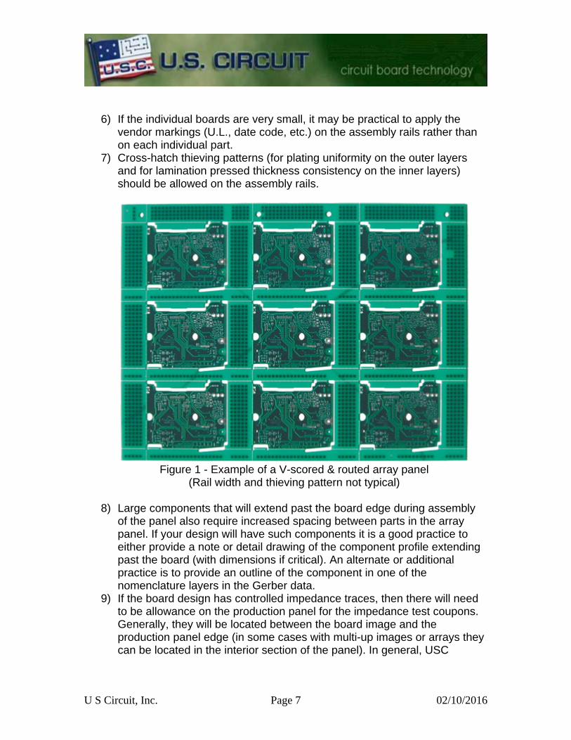
7) Cross-hatch thieving patterns (for plating uniformity on the outer layers and for lamination pressed thickness consistency on the inner layers) should be allowed on the assembly rails.
Figure 1 - Example of a V-scored & routed array panel
(Rail width and thieving pattern not typical)
8) Large components that will extend past the board edge during assembly of the panel also require increased spacing between parts in the array panel. If your design will have such components it is a good practice to either provide a note or detail drawing of the component profile extending past the board (with dimensions if critical). An alternate or additional practice is to provide an outline of the component in one of the nomenclature layers in the Gerber data.
9) If the board design has controlled impedance traces, then there will need to be allowance on the production panel for the impedance test coupons. Generally, they will be located between the board image and the production panel edge (in some cases with multi-up images or arrays they can be located in the interior section of the panel). In general, USC
U S Circuit, Inc. Page 8 02/10/2016
requires an additional 0.750” space for the coupon (plus 0.100” space between part and coupon).
10) Please note that our longest production panel measures 24.0”, so the panel design must fit within the usable potion of the panel, which is typically 22.0” (a standard 1.0” panel border allows room for lamination, imaging and drill tooling). If your design exceeds 22.0” but is less than 24.0” contact USC customer service for discussion on special processing options.
11) Additional or special coupons: IPC Class 3 and military coupons are common at USC. In general, we can add Class 3 coupons in a production panel border of 1.5”, so please take this into consideration when requesting a Class 3 or military quote. USC can incorporate additional quality, engineering, or compliance coupons (such as IST coupons)—please provide dimensions or scaled drawing to the customer service department when requesting a quotation.
Materials
Printed Circuit Boards (PCBs) are generally constructed from the three basic material types; copper foil, laminate cores, and bonding prepreg. Copper Foil Cores as well as the outer layers of multilayer PCBs are laminated with copper foil in thicknesses that are determined by weight per square foot (i.e., 0.5 ounce, 1.0 ounce, 2.0 ounce, etc.). USC builds boards with copper foil as thin as 0.375 ounce up to a very heavy 5.0 ounces. Thinner or thicker copper weights are available by special order (and include special process considerations). The major design constraint when it comes to using heavier copper weights is the width of traces and overall size of copper features—the heavier the copper the larger the associated feature designs must be. Etch factors must be applied to artwork to compensate for the etch profile (which increases with copper weight). In general, 1 mil (0.001”) per ounce of copper is applied to the line width to finish back at nominal after etching. For example, a 3.0 ounce copper foil must have an additional 3 mils of etch factor applied to the lines and features, so a starting line width of 0.005” becomes 0.008” before etch, and yields the nominal 0.005” thereafter. So very fine line designs (and their associated narrow spaces) are sometimes not possible to build using heavy copper weights. IPC design standards as well as USC technical personnel can assist you with design considerations when heavy copper foils are required.

U S Circuit, Inc. Page 9 02/10/2016
Core Material
Core material is e-glass cloth sheets and resin (prepreg) pre-laminated into a cured (commonly called “C-Stage”) double-sided copper clad panel, which is pre-cut by the material supplier to the standard production panel sizes stocked by USC (i.e., 16” x 18”, 18” x 24”, etc.). The cores are also stocked in common thicknesses starting at 2 mils (0.002”) up to approximately 40 mils (0.040”). Double-sided “rigid” material is also stocked in the common thicknesses of 0.059”, 0.093”, and 0.125”. Combinations of core thicknesses with prepreg bonding sheets are used to construct multilayer boards. Prepreg Material Prepreg bonding sheets is simply the resin coated e-glass cloth in a semi-cured form, commonly referred to as “B-Stage”. The resin will flow during lamination and will fully cure into a “C-Stage” condition by the end of the press cycle. The e-glass sheets come in several common weaves and thread counts—USC stocks the following designations: 106, 1080, 2113, 3313, 2116 and 7628 The cured thickness of the different prepreg styles depend entirely upon the weight of the opposing foil, whether it is a plane or signal layer design, how sparse or dense the circuitry is, and the distribution of copper features. That is why it is very difficult to provide an exact thickness for prepreg styles (and for designers to pre-configure every sheet in a stackup design). For this reason it is best to let USC engineering determine the best stackup to meet your overall thickness and impedance requirements.

U S Circuit, Inc. Page 10 02/10/2016
IPC-4101 Base Materials – “Slash Sheet” Reference Example:
USC stocks materials that are suitable for simple double-sided designs up through high speed digital and lead-free (Pb-free) assembly process compatible (and/or RoHS compliant). Please state requirements on associated drawing or purchase order.
High Performance Laminates Besides FR-4 laminates in high-Tg resin formulations, USC also stocks
high frequency, high temperature/severe environment, lead-free assembly compatible and RF-compatible materials.
Isola 370HR, 185HR, FR406, I Speed Nelco N4000-13, N4000-13EP and N4000-13EPSI Rogers Corporation 4003 and 4350 (with 4450 prepreg) Polyimide (IPC-4101 /40, /41 or /42) Laird Technologies Aluminum-backed specialty laminates Totking Aluminum-backed specialty laminates
Traces, Pads & Features Inner layer features are generally much easier to reproduce in manufacturing due to the fact that it is simply a print and etch process rather than the additional copper plating that is required on the outer layers (with the exception of sequential laminated stackups). For this reason there are typically two sets of design rules for PCB features—inner layer and outer layer rules.

U S Circuit, Inc. Page 11 02/10/2016
Line Width & Spacing In manufacturing we must add etch compensation to the artwork for both internal and external layers—in general finer line and space can be more easily accomodated internally (given the same copper foil weight). Except for special circumstances the USC rule is to add 1 mil (0.001”) of etch compensation for each ounce of copper (foil + plating on the outers). Example 1: Designed line width of 8 mils on a 1 ounce copper foil layer 3 (of a 6 layer design) will measure 9 mils on the artwork after etch compensation, and is expected to return to the nominal 8 mils after the etch process. Example 2: Designed line width of 8 mils on a 2 ounce copper foil layer 2 (of a 6 layer design) will measure 10 mils on the artwork after etch compensation, and is expected to return to the nominal 8 mils after the etch process. Example 3: Designed line width of 8 mils on a 1 ounce copper foil layer 1 (of a 6 layer design) will measure 10 mils on the artwork after etch compensation, and is expected to return to the nominal 8 mils after the etch process. Assume there will be 1 ounce of plated copper in addition to the foil weight. An important area of concern for designers is to consider the differences in inner layers and outer layers simply because of the added plating process on the outers. The most common plating process is called pattern plating, because the only features that are plated are the patterns created by the artwork image. And patterns with isolated features will plate up faster and greater than more densely patterned areas of the board due to the process, so the following design guidelines will help assure a more uniform product:
1) Maintain uniform copper feature density and placement on the outer layers. If possible design the outers so that they are uniform and do not have isolated features. Isolated traces will plate up more, and isolated plated holes will also plate more, resulting in possible undersize holes (if the same pilot drill size is used as compared to holes in densely populated areas).
2) Route isolated traces on inner layers if possible, to maintain a more uniform outer layer pattern.
3) Impedance controlled traces (which require strict width and thickness control) are more easily maintained on internal layers. “Bury” impedance traces within the board if possible.
4) If isolated features cannot be eliminated on outers, then design (or allow the addition of) thieving patterns in the open areas adjacent to the isolated traces, etc. Thieving patterns are typically small squares or a cross-hatch pattern of copper that are placed at least 50 mils (0.050”)
U S Circuit, Inc. Page 12 02/10/2016
from any board feature to more evenly distribute the pattern for uniform plating. The same patterns are desirable on inner layers too, but for a different reason (they maintain copper balance for uniform lamination thicknesses).
Annular Ring
Annular ring is defined as the minimum distance between a drilled hole
and the circumference of its associated pad. For a 10 mil (0.010”) drilled hole in a 20 mil (0.020”) pad, the annular ring is defined as 5 mils (0.005” per side) assuming perfect registration. Minimum annular ring is that distance between a non-centered hole where it is closest to the pad edge.
IPC defines minimum annular ring more strictly for Class 3 designs vs.
Class 2 designs. For that reason alone it is good practice to maintain a minimum of 5 mils per side (drill size plus 10 mils) in the design if the board is to be high reliability, military, or Class 3 specification.
If tangency is allowed (drilled hole edge coincides with pad edge) then
there will still be an annular ring of typically 1 mils (0.001”) due to the plating thickness in the barrel of the hole. This is generally acceptable for via holes in IPC Class 2 designs. It is also generally acceptable for oblong or “football” shaped pads where the edges in one axis are closer to the hole than the other axis by design (such as in some connector hole designs). Teardropping Teardrops refer to the shape of drilled hole pads that are typically associated with via interconnect holes, whereas the pad is elongated and enlarged at the trace/pad junction to prevent a possible electrical open if the drilled hole is mislocated or is tangent at that junction. If the teardrops are not included in the design as received from the customer, then USC will ask if it is acceptable to add teardrops. There are two common shapes—a “snowman” style that is basically the radius from another pad added in the direction of the trace, and the more popular traditional teadrop shape which is basically a fillet extending from either side of the trace to the associated pad.

U S Circuit, Inc. Page 13 02/10/2016
Figure 2 - Teardrop Pad Styles Unterminated (Hanging / Dangling) Traces Traces that originate normally from a feature or pad that have no
termination on the other end (i.e., pad, surface feature, etc.) are called by various names such as “hanging traces” or “dangling traces”. For clarity USC calls these “hanging traces”. They may be trace stubs that are left over from the design process that did not get deleted during the clean up process, or are legitimately unterminated signal traces that are meant to extend to a nearby pad or other feature. USC will always bring these traces to the designer’s attention so that they may be deleted or connected to the proper feature.
Non-Functional Pad Removal Pads that are not connected to any electrical features on the internal
layers are called non-functional pads. They typically are located within clearances on plane layers, which provide additional opportunities for shorts, etc. as well as shorten drill life (increased metal layers). It is recommended that they be removed at the design stage, but if not USC may request authorization to remove them when tooling the part for production.
Thieving As mentioned in the section on traces, if isolated features cannot be
eliminated on outers, then design (or allow the addition of) thieving patterns in the open areas adjacent to the isolated traces, etc. Thieving patterns are typically small squares or a cross-hatch pattern of copper that are placed at least 50 mils (0.050”) from any board feature to more evenly distribute the pattern for uniform plating. The same patterns are desirable on inner layers too, but for a different reason (they maintain copper balance for uniform lamination thicknesses).
U S Circuit, Inc. Page 14 02/10/2016
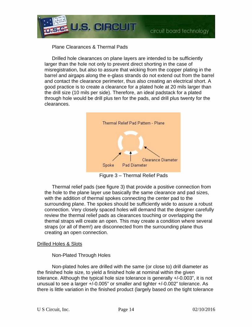
Plane Clearances & Thermal Pads Drilled hole clearances on plane layers are intended to be sufficiently
larger than the hole not only to prevent direct shorting in the case of misregistration, but also to assure that wicking from the copper plating in the barrel and airgaps along the e-glass strands do not extend out from the barrel and contact the clearance perimeter, thus also creating an electrical short. A good practice is to create a clearance for a plated hole at 20 mils larger than the drill size (10 mils per side). Therefore, an ideal padstack for a plated through hole would be drill plus ten for the pads, and drill plus twenty for the clearances.
Figure 3 – Thermal Relief Pads
Thermal relief pads (see figure 3) that provide a positive connection from
the hole to the plane layer use basically the same clearance and pad sizes, with the addition of thermal spokes connecting the center pad to the surrounding plane. The spokes should be sufficiently wide to assure a robust connection. Very closely spaced holes will demand that the designer carefully review the thermal relief pads as clearances touching or overlapping the themal straps will create an open. This may create a condition where several straps (or all of them!) are disconnected from the surrounding plane thus creating an open connection.
Drilled Holes & Slots
Non-Plated Through Holes Non-plated holes are drilled with the same (or close to) drill diameter as the finished hole size, to yield a finished hole at nominal within the given tolerance. Although the typical hole size tolerance is generally +/-0.003”, it is not unusual to see a larger +/-0.005” or smaller and tighter +/-0.002” tolerance. As there is little variation in the finished product (largely based on the tight tolerance
U S Circuit, Inc. Page 15 02/10/2016
of the drill tools themselves) we even see a +0.001” / -0.002” tolerance occasionally. As always, if it is not necessary to achieve a tight tolerance, we appreciate the largest reasonable tolerance in order to assure ease in manufacturing and 100% compliance. Sometimes it is desirable to have a surface pad associated with the non-plated hole. In that case it should (as good practice) be a minimum of 0.010” larger than the associated hole size. In other words, if the pad is the same size or smaller than the hole, it will not exist! This sounds too logical and is a simple concept, but it is surprising how many designers place a pad on the outer layers that is the same or smaller size than the hole and we have to ask if they want us to remove it or make it larger—time and energy wasted! If it is only a “place holder” to identify the location of the non-plated holes in the Gerber data, then please make a note in the readme.txt file or on the associated drawing whether or not to remove or to enlarge the non-plated through hole pads on the artwork.
Plated Through Holes Plated through holes serve two purposes on a circuit board—the first it to provide electrical connectivity (via holes) and the second is to provide a solderable conduit for a component device. Via holes should generally have no specific finished tolerance as it is not critical what size they finish, only that they meet annular ring specification and minimum copper plating specification. In that case a tolerance of +0.003” / -<diameter> is common and good practice. For example, a 0.010” finished hole size for a via interconnect hole that does not have any solderable components associated with it should have a tolerance of +0.003” / -<diameter> (+0.003” / -0.010”). That way it can finish the standard tolerance larger (desirable if the board is thick and aspect ratio determines that a larger via size will provide higher copper plating reliability assuming the pad is large enough, or it can finish any size smaller than the specified size as it does not matter if it even gets close to closing up with the copper plating. Component holes that are plated through have a typical tolerance of +/-0.003”, although it may be tighter for some critical holes. Holes that are considered more critical would be press-fit component holes, so a tolerance of +/-0.002” is common for those types of connectors and components. However, an even tighter tolerance than +/-0.002” is not recommended as it becomes more difficult to assure compliance, particularly with thicker designs or those with high copper plating requirements.

U S Circuit, Inc. Page 16 02/10/2016
Slots
Slots are designed in both plated and non-plated through configurations,
with the same considerations as standard holes when it comes to tolerances—that is, it is generally easier to meet a tighter non-plated tolerance than a plated one. Having stated that, the major difference is that slots in both configurations do generally come with higher tolerances, with +/-0.005” being the most common. That is because the width is determined by the diameter of the drill (or slot-type drill or router bit used), but the length is determined by the path of that slot-bit or router, which usually requires a higher tolerance of +/-0.005” For that reason and for simplicity, the tolerance is expressed as +/-0.005 overall rather than +/-0.003” for width and +/-0.005” for length. If a tolerance of less than 0.003” is called out we will usually request a deviation, so try not to specify critical slot tolerances—go with +/-0.005” if at all possible. Slots with width larger than 0.250” must not be less than +/-0.005” as there is more natural variation in the process used to produce them.
The length of the slot is generally expressed as total length including the
radius on each end. The location dimensions (if not included in the Gerber data package) may be expressed on the associated drawing by providing center point location as an X/Y coordinate in respect to zero datum, including a figure or detail showing orientation with length, width and end radius.
Routed Holes
Routed holes are those that exceed typical drill sizes (in general diameters above 0.250”) as large drills place an exceedingly high torque on drill machine air-bearing spindles that must also accommodate extemely accurate small drill diameters. So if the holes are plated through, then they will be routed at the primary drill stage (before plating operations). If the holes are non-plated, then they will be opened at the final NC Routing stage of production (after plating operations). Tolerances apply much like slots, as the diameter is created by a smaller router bit travelling in an arc as opposed to a true diameter drill bit, so larger tolerances apply. Typically, a tolerance of +/-0.005” is specified for holes larger than 0.250” (both plated and non-plated through).
Drill Charts & Tables The pilot drill size for a plated through hole usually varies a bit between fab shops, because it is tailored to their plating process. For that reason refrain from providing pilot drill sizes—only finished hole sizes, so that the shop may select the appropriate pilot size based on their process chart. Exceptions to this rule exist only for critical hole sizes associated with press-fit connectors and components, so sometimes through experience the designer is asked to specify

U S Circuit, Inc. Page 17 02/10/2016
both pilot and finished hole size. If this can be avoided please do, as most shops will occasionally request a deviation by a mil or two so as to assure that the press-fit holes finish within the stated tolerance.
Finished Hole Size Number of Sizes Larger Pilot Drill Size 0.006” – 0.010” One Drill Size Larger 0.008” – 0.012” 0.012” – 0.018” Three Drill Sizes Larger 0.014” – 0.021” 0.020” – 0.025” Four Drill Sizes Larger 0.024” – 0.029” 0.026” – 0.069” Five Drill Sizes Larger 0.031” – 0.073” 0.069” – 0.260” Six Drill Sizes Larger 0.075” – Up
Figure 4 – Typical Pilot Hole Size Table The typical pilot hole size table shown in figure 4 is based on standard plating requirements for IPC Class 2 and 3 boards (i.e., 0.001” Cu in PTH). If there are higher plating requirements (i.e., 0.0015” Cu in PTH) or more than 1.0 ounce average plating, then there will likely be an additional 0.001” – 0.005” added to the pilot hole size. For example, a 0.010” finished hole size (FHS) with a standard pilot drill size of 0.012” will be drilled with a 0.014” if 2.0 ounce copper plating is specified.
Back Drilling
Back Drilling is a term generally used to express a controlled depth non-
plated non-through hole drilled from one side of a multilayer board. The hole may be used for via stub removal in designs with critical signal requirements, or it may be to remove partial plating from a press-fit type connector hole. Obviously, different applications demand different specifications and tolerances. In general though, the depth of penetration should be specified to be no tighter than +/-0.005”. Other specifications may be the diameter required (typically over the plated hole size for thorough plating removal, etc.), or the minimum (remaining) dielectric between the penetrated and non-penetrated layers.
Drill files should be separated for each different depth required in a given
design (if more than one depth is specified). They should also clearly state from which side of the board they are to be drilled (component or solder side, from layer 1 to layer n, etc.).
Via-in-Pad
Designers are constantly forced to consolidate designs to meet restrictive
form factors. One of the ways to effectively reclaim real estate and at the same time shorten transmission line lengths is to employ via-in-pad
U S Circuit, Inc. Page 18 02/10/2016
technology. This term generally describes an interconnect via hole that is co-located in a solderable surface feature. In most cases the attachment of the component during assembly is negatively affected by the presence of a hole where the solder paste resides, and which can lead to solder voids and in the case of ball-grid arrays—ball voiding and outgassing. So it is usually required that these holes are filled with a resin-type material (typically non-conductive), cured and then plated over by the final plating cycle so that only the slightest dimple or mark on the pad remains. This provides a planar, void-free surface for device attachment at assembly. Due to the processing steps required, filled via-in-pad adds an extra day to the lead time with added cost accordingly. It requires multiple plating cycles, epoxy filling, curing, planarization, direct metallization and then final electrolytic plating to achieve the desired results. It is recommended that designers follow the well-established rules expressed in IPC-2226, 6012, and A-600 to avoid problems and pitfalls. If you have specific questions, it is always best to contact USC engineering for assistance during the initial design phase of your project.

U S Circuit, Inc. Page 19 02/10/2016
Soldermask & Legend
Webbing – Minimum Width
Soldermask webs are the thin lines of mask between surface mount pads, which serve the function of preventing solder bridging during assembly. To stay on the board with good adhesion they must be a minimum width of 0.003”. Also, they must be at least 0.002” from the surface feature to allow for registration tolerance. That means that any feature that has a space to the next feature of 0.006” or more can have soldermask webs between them—any closer and the features must be clear of soldermask in between. That is why fine pitch surface mount pads are often “gang relieved” or “windowed” in the soldermask layer because they are too close together to allow for a minimum width soldermask web.
“Gang Relief” or “Window” Soldermask – No Web
Figure 5 In figure 5 above is a simple representation of a “gang relief” or
“window” soldermask clearance surrounding fine pitch surface mount pads, such as a QFP device, etc. In the following figure 6 is a simple illustration of a soldermask web that is between the surface mount pads—assumably large enough spacing between pads which allows minimum soldermask web width of 0.003”.
U S Circuit, Inc. Page 20 02/10/2016
Figure 6 – Soldermask Web
Edge Finger Guidelines Soldermask clearance around gold plated fingers on the edge of
the board would seem to be common sense, and it is when referring to keeping the end of the fingers where the bevel will be clear of mask. However, there are a few considerations to take into account when planning the clearance line at the top of the fingers.
The soldermask should not extend up past the top of the fingers,
which exposes the associated traces. The traces may be subject to damage at the Nickel-Gold tip plating process. It is good practice to extend the clearance line down to the very top of the gold fingers—tangent to the top where they meet the associated trace. This keeps the traces under the mask yet allows the full contact finger to be exposed to the plating process.
Also, any via holes that are designed very close to the soldermask
line of demarcation must be filly covered with mask as well—a minimum distance of 0.050” should be designed into the distance from edge of associated pad to soldermask clearance line. If this is not possible, then the designer should (or allow the fabricator to) bring the soldermask line down onto the top of the fingers assuring a minimum distance away from the via hole edge.
Via Plugging Via plugging is a process that sounds simple and easy at first, but
there are more than a few important considerations that must be taken into account before specifying via hole plugs. The associated drawing should clearly state which hole size (vias) should be plugged, and from which side of the board (top/bottom or component/solder). Holes SHOULD NOT be plugged from both sides, as this can allow entrapped gases to violently escape during assembly. If only a portion of the designated hole size should be plugged (or if a partial from each side is plugged), then separate design files should be provided to the fabricator.

U S Circuit, Inc. Page 21 02/10/2016
BGA Plugging Because BGA footprints have tight spacing between surface pads
and their associated via holes, the necessity to plug the hole is to prevent solderpaste from drawing down into the vias from the nearby pads. Obviously, BGA vias should be plugged from the BGA pad side of the board. Now if the BGAs are designed with the vias located directly within their associated pads, then that calls for a different method—via fill.
Via Fill – Conductive & Non-Conductive The via fill process requires considerably more time and process
steps, but is necessary when via holes are co-located in solderable pads, or for internal (buried vias) in high-aspect ratio designs to help prevent large volumes of entrapped air. In both cases the simplified process is to completely fill the holes with a thermally-cured epoxy paste after plating the holes, and then to planarize and plate over the surface pads after thermal curing. Via-in-pad designs then eliminate the risk of drawing solderpaste down into the associated holes.
There are two types of epoxy fill—conductive and non-conductive. Since
both can have their cured and planarized caps treated with direct metallization and then completely plated over with electrolytic copper (as well as the final surface finish) the main difference is usually determined by the board design and intent for the via-in-pads. If it is purely electrical—that is the vias will interconnect electrically as normal then the barrel of the hole conducts the current and conductive fill is not required. If the vias are used to draw heat away from a component body, then a conductive epoxy via fill material will aid in thermal excursion.
Regardless of type of via fill It is necessary to note the requirement
when submitting for quotation as the process costs more and takes longer to complete. The board quote will reflect this with additional cost and lead time added accordingly.
Legend (aka: Characters / Nomenclature / Silkscreen) Legend is known by several names depending upon the OEM or
facricator, but legend is the most universal of them. The term silkscreen actually refers to the process that is used to screen the ink on the boards, although modern methods using ink-jet machines has become the standard. The common element is that the legend is used to identify the name and/or location of the components that are to be placed on the board at assembly. With the advent of pick-n-place chip shooters taking the place of hand assembly, it is less necessary

U S Circuit, Inc. Page 22 02/10/2016
to have a legend on the board, although it is still handy when troubleshooting or performing field service on the finished goods. Higher density designs that require finer legend characters are problematic in that the smaller characters tend to smear and run together if smaller than the minimally recommended line width and character height. In addition when “clipping” the charcters over solderable surface features (more on this next) the legibility can be destroyed if the characters are too small. To maintain legibility USC recommends a character width of no smaller than 0.005”, and a character height no less than 0.035”. Even at these minimums, it is difficult to maintain legibility if design placement has the nomenclature running over or on top of solderable pads. To prevent any ink on the pads, the legend must be “clipped” (removed at soldermask clearances) to eliminate encroachment on solderable surfaces. As can be imagined, this can destroy any legibility if the characters are ill placed or too small. Please consider this at the design phase. In some cases, we can move some nomenclature away from solderable surfaces with space permitting, but only for a couple of places—this is a time consuming process and prone to human error, so good design is preferred. Vendor markings (i.e., U.L. logo, flammmability rating, date code, etc.) are also generally placed in the silkscreen layer (if not specified to be placed on the outer layer component or solder side artwork). These markings can usually be sized to fit specified locations, but the necessary size (width and height) of the characters to maintain legibility need to be considered as well. If the part is extremely small and/or located in an assembly array we may request permission to place the vendor markings on the rails instead of the individual parts. Mechanical Drilling There are a few metrics that should be considered when designing a board—minimum and maximum hole size, and aspect ratio of the smallest holes (ratio of diameter to depth).
Mechanical drilling (using carbide cutting tools) limits diameter to a minimum of 0.005” (smaller holes are typically laser ablated in modern designs) and a maximum Hole of approximately one quarter of an inch (0.250”—larger tools place too much stress/torque on accurate air-bearing machine spindles used to drill the boards). Larger holes are typically routed using router bits on a machine designed to handle side-loads on a cutting tool. In that respect, a standard (typical) tolerance of +/-0.003” in diameter for drilled holes must be
U S Circuit, Inc. Page 23 02/10/2016
expanded to routed holes >0.250”—typically +/-0.005”. Positional accuracy is rarely defined as that is largely determined by the drilled hole’s associated pad and remaining minimum annular ring specification. The metric other than diameter that is important is the aspect ratio of small (typically via) holes. The smaller the hole, and the thicker the board, the more issues can arise during manufacturing. Most notable is the plating profile, which is determined by the “throwing power” of the plating process—this determines the copper thickness variation between the outer and inner barrel of the plated hole. Also, higher aspect ratio holes are more easily plugged with debris, can experience local plating voids, and are more difficult to smoothly drill creating roughness which leads to plating folds and inclusions. Maintaining a lower aspect ratio assures quality performance, so unless absolutely necessary due to mitigating design factors it is best to allow for the largest via holes size when thicker boards are designed. As a general rule, aspect ratios greater than 10:1 require special processing consideration and/or process steps. An example would be a 0.010” (as drilled) hole in a 0.100” thick board, which is 10:1 aspect ratio. If the drilled hole size were 0.008” in the same board, the aspec ratio would be 12.5:1, which requires special consideration. Please contact USC engineering at the design phase if ratios greater than 10:1 are required. Scoring
Figure 7 – V-Score Web
Scoring or V-Score is a process that cuts a notch or channel into the board on both the top and bottom side which facilitates the easy snapping apart of individual parts from an array panel after assembly. Unlike tabs (with or without perforation holes) the parts need not be separated by a gap—they can be arrayed edge-to-edge (if the edge is straight without routed features). Several score angles are available, but 30 degrees is the most common (and preferred).
U S Circuit, Inc. Page 24 02/10/2016
The depth is typically expressed in terms of the remaining “web” in the center of the board at the score cut (see Figure 7). The web thickness is commonly specified to be one-third of the board thickness (ex: for 0.062” thick boards). So with a 0.062” thick board the web would be specified to be 0.021” thick. The tolerance is typically + 0.003”/-0.005”. If a greater angle is specified (such as 45 degrees) the width of board stock affected by the V-score cut is increased. So another very important design metric needs to be remembered when specifying V-scoring—the distance away from ANY internal copper feature. Consider that there may be stresses placed on any features and/or components that would be located close to the edge as the act of singulating the boards could lead to fractures or lifted copper in the general vicinity. So to be sure keep all features at least 0.010” away from the score line (USC recommends as much as 0.050” if available). A minimum and maximum panel thickness is required when specifying V-scoring. The thinnest panel is approximately 0.020” and the thickest is 0.125” (a common multilayer board overall thickness). There will be obvious scoring and/or panel problems if boards are outside this thickness range. Routing CNC Routing (Computer Numeric Control Routing) is the process used to cut the final board outline from the surrounding production panel (or to cut the final array panel from the production panel). The machine follows the dimensioned X/Y coordinates as provided in the design data (Gerber data and/or associated mechanical drawing). The standard fabrication tolerance is +/-0.005”, which is generally expressed as a drilled hole to edge (in both X and Y axis). If a dimensionally correct outline is not provided in the Gerber data, then it is mandatory that at least one drilled internal hole to edge is provided, in order to accurately orient the outline with the board feature image. At this time the non-plated slots and larger holes are fabricated, as well as separation of test coupons from the panel. If there are countersunk holes or special milling requirements the fabrication department will address them in the appropriate order. After separation of the board from the panel, the edges will be smoothed and inspected to be sure there is no exposed copper from internal planes and/or features that were exposed by the fab line. This is why it’s important to relieve all planes and features from the designed edge of the board by at least 0.010”—if the design requires copper features running right up to the edge of the part please note this on the associated drawing or in the Gerber data readme.txt file. If there are no notes and copper will be exposed by routing, USC engineering will contact you for approval to “pull back” the copper from the edge.

U S Circuit, Inc. Page 25 02/10/2016
If breakaway tabs are not designed into the array panel (either in the Gerber data or detailed on the associated drawing) then USC engineering will place the tabs in convenient locations based on the overall board design and customer preferences (perforations—size and number of holes, combination score/tabs, etc.). Unless otherwise specified, we will design a nominal 0.050” -0.100” wide tab with 0.010” - 0.020” perforation holes (aka: “mouse bites” or “rat bites”). The height of the tab will be 0.100” as well, as the array will be designed with a typical 0.100” routed channel between the boards. If there is a component that extends further out from the edge of the board and there should be no tabs in that area (or even a greater separation to the adjacent board in the array) please note it on the drawing or highlight the component by providing its outline in the silkscreen layer (a common practice). Beveling Edge contact fingers or tabs are typically beveled on the edge to facilitate ease of insertion into the corresponding connector. The beveling operation usually takes place after the board has been routed from the production panel (unless they are recessed or there are special process considerations, etc.). There are three dimensions associated with the bevel—angle in degrees, depth from edge, and width of the remaining board at end of bevel. Only two of the three dimensions may be specified, as by specifying all three the tolerance is rendered irrelevant. Generally only angle and depth are specified. By holding these two dimensions the calculated edge width is automatically created. Bevel angles may be specified from 20 to 60 degrees in 10 degree increments (with a commonly used 45 degree bevel included). Bevel depth is based on the amount of remaining width desired. A too-deep bevel may bottom out too early in the connector and not seat properly, so the connector metrics should be considered in the board bevel specification. In general, it is better to specify a shallower rather than deeper bevel. A final consideration is the location of the fingers (and the extensions used for electrolytic plating) in relation to the bevel depth. Ideally, where the contacts end is where the bevel begins (it also removes the entirety of the finger extensions). USC will usually extend the contact fingers to the point where the bevel begins to facilitate this (if they are not the correct length by design). Milling Milling on a PCB is typically used to reduce the thickness on the edge of the card, thus allowing a thicker board to fit easily into a card guide or rack.
U S Circuit, Inc. Page 26 02/10/2016
There are only a few rules to consider when specifying milling—besides
the width from the edge of the board and the depth (which can be specified by dimension of the milled zone or dimension of the remaining board thickness), be sure to consider the following:
1) “Pull back” all copper features (planes, circuits, etc.) by at least 0.010” from the edge of the milled zone.
2) Clearly specify which side of the board is to be milled—use a detail on the associated drawing to visually clarify if necessary.
3) Remember that only one side of the board shall be milled (top or bottom side)—milling from both sides leaving an unsupported edge is discouraged.
4) A minimum milled zone tolerance of +/-0.005” in both width and depth is required.
Counter-Bores and Counter-Sinks Also referred to as counterbores and countersinks, these are facilitated at the CNC Routing stage of manufacturing unless they are associated with plated features (where they will be created after drilling prior to plating). Standard symbols and drawing examples from ASME Y14.5M should be used to show dimensions (width, depth, tolerance, etc.) and clearly marked on which side of the board they are to be located (top/bottom or component/solder). Another commonly overlooked issue is whether or not they are to be plated—please be sure to state accordingly.
Surface Finishes HASL Hot Air Solder Leveling (HASL) has been the solder finish replacement for fused tin-lead plating for many years. The best characteristic is that “nothing solders better than solder”, but it does have a few drawbacks—it is not a very planar surface and not recommended for fine-pitch BGAs. It is also not a RoHS compatible finish due to the lead content (lead-free versions are available if specified). But for economical standard through-hole board designs it is tough to beat. The intermetallic formed at assembly is Tin from the solder with the underlying Copper plating on the feature (Sn/Cu). Shelf life is excellent, with 1 year (or more) in a controlled environment prior to assembly.

U S Circuit, Inc. Page 27 02/10/2016
ENIG
Electroless Nickel Immersion Gold (ENIG) has the answer to HASL’s planarity problem—it is flat, uniform, and provides a dependable surface for fine-pitch BGAs and small passives (0402s, 0201s, etc.). The gold is very thin by design and is only there to protect the underlying Nickel layer from passivation (oxidation). When the solderpaste liquifies, the gold dissolves into the bulk solder and the intermetallic is formed between the Tin in the solderpaste and the Nickel layer that was under the gold (Sn/Ni). Per IPC the thickness of the Electroless Nickel is typically 125 – 150 microinches, and the thickness of the Immersion Gold is typically 2 – 3 microinches. In the ENIG plating process, the gold deposits as it replaces Nickel ions, leaving a Nickel-Phosphorous layer thereafter. It is this Nickel-Phos layer that can be problematic if there is too much Gold specified, as it grows when Nickel is replaced by Gold ions. In the past, some designers thought that more Gold would be better at protecting the Nickel, whereas it was actually worse! The result was a phenomenon that was known as “black pad”, and was notorious for causing poor solder joints and interfacial fracturing of BGA attachments. So the bottom line is each chemistry supplier (and associated fabricator) has determined the optimum amount of Gold to plate per their particular process, and it is understandably different for each one (i.e., Uyemura, OMG, Atotech, etc.). Here at USC our process is optimum at 2 – 3 microinches, so if a higher Gold thickness is specified we will request a deviation to the proper thickness for our process, which will yield quality parts. Also bear in mind that ENIG is designed as a solderable surface, and is not intended to be treated like hard gold plated circuits (i.e., under the soldermask layer). So it is best to also specify soldermask over bare copper (SMOBC) with ENIG as the final finished for all exposed solderable land areas. Shelf life is 1 year in a controlled environment prior to assembly. Immerision Ag (Immersion Silver) Immersion Silver surface finish is similar to ENIG in that it is very flat and provides an excellent planar surface for fine-pitch devices. The main difference is instead of the assembled intermetallic being Sn/Ni as with ENIG; it is Sn/Cu as with HASL, but without the planarity issues and lead content. Immersion Silver has a few different formulations offered by the main chemistry suppliers, but the most common is MacDermid Sterling, which is what USC is using. As with ENIG the process will perform best using the supplier’s recommended thicknesses. The Immersion Silver coating is very thin (6 – 18
U S Circuit, Inc. Page 28 02/10/2016
microinches) and is deposited directly on the plated copper surface features. When the solder paste liquifies, the Silver dissolves into the bulk solder and the intermetallic forms between the Tin (Sn) in the solderpaste and the Copper (Cu) on the board. Since there is no Lead the finish is RoHS and Pb-free compatible. The only detriment is that the shelf life is typically shortened with Immersion Silver—the supplier recommends a maximum of 6 months in a controlled environment prior to assembly. Immersion Sn (Immersion Tin) Immersion Tin is not as popular a surface finish as compared to HASL, ENIG and Immersion Ag. Perhaps the most common use has been for backplane assemblies as the Tin provides good lubrication for press-fit component insertion. However, it remains a viable finish for standard circuit boards when a Pb-free finish is desired. ENEPIG (Electroless Nickel / Electroless Palladium / Immersion Gold) This finish is generally used for hybrid designs, where solderable pads and wire-bond pads exist on the same board, as the finish is friendly to both. With soldered components, the Gold and Palladium layers dissolve into the solder joint much like ENIG, and the resulting intermetallic is Sn/Ni. There is enough of the Gold and Palladium for wirebonding, and it is a more cost-effective finish when compared to higher Gold thickness finishes (Electroless Hi-Build Gold or Electrolytic Soft Gold). Electrolytic Hard & Soft Gold As the name states these finishes are electro-plated rather than immersion technology. The process differences are such that the surfaces that are to be plated must be electrically connected during the process, and may be etched only once the finish is complete (as the base copper foil is the conductor). So the finish is typically used as a subsequent etch resist, and thicknesses of both the Nickel layer and the underlying Copper foil and plate must be controlled carefully to avoid undercut. What this means to the designer is that the finish is not typically used for high copper weight designs—a thin copper foil and minimal overplate are recommended for best results. The benefits are that that multi-level thicknesses of Gold can be selectively plated on the Nickel, to lend itself to both solderable and wirebondable assembly (thinner Gold for soldering and thicker Gold for wirebonding). Hard Gold also holds up well to abrasive environments or repetitive contact, so for designs such as test probe cards it is an excellent finish.

U S Circuit, Inc. Page 29 02/10/2016
Electroless Soft Gold (Wirebondable) For chip-scale products—multichip modules and such it is common to specify a soft Gold wirebondable finish, but with process characteristics that are friendly to small etched features. Electroless soft Gold (aka: Electroless Hi-Build Gold) is typically plated up 8 – 15 microinches over a “seed layer” of ENIG. So the immersion Gold helps provide a good bond between the Nickel underplate and the electroless Gold on top. Being immersion technology, the finish may be applied post-etch, so feature undercut is not an issue. This finish is not usually specified for mainstream printed circuit boards. OSP (Organic Solder Preservative) OSP was believed to be the finish of the future, as it is a very thin organic coating that is clear, cost effective, easy to apply and control, and very assembly friendly (for one or two thermal excursions). It is known almost exclusively in the USA by Entek, as the Enthone Corporation’s trademark chemistry became the leading brand used by most all fabricators. The thickness is typically a very thin 20 – 50 microns (35 microns nominal), and has no effect on the resulting solder joint (Sn/Cu intermetallic). It has become the leading surface finish in Japan, (Shikoku & Entek) where fine-pitch PCBs are the norm (computers, camcorders, cell phones, etc.). Its only real detriments are ability to survive multiple thermal excursions during assembly or rework (it usually “burns off” quickly), and its limited shelf life (typically 3 months recommended). But regardless, it is a Pb-free, RoHS compatible (Pb-free process specialized OSP is available) and extremely cost-effective finish. SN100 (Sn99.5/Cu0.5) Pb-free HASL This is USC’s most popular lead-free compatible solder coating finish, which provides a R0HS compliant solder finish that is also lead-free assembly process compatible. Although the flatness is somewhere between standard HASL and the planar finishes, it is an excellent choice when a solder type finish is desired. It is not as common as ENIG or Immersion Silver, so USC still outsources this finish at the current time. Carbon Ink Once very popular for on-board keypad sensors etc., Carbon Ink is no longer specifed as often as it once was (except for specialized niche product designs). It is still the best choice when a finish that exhibits thickness and resistance to direct contact is desirable. Carbon Ink is also used where a specified electrical resistance is required, as the ink is available in several ohm (resistance) specifications. USC uses the Electra d’or brand of Carbon Ink.

U S Circuit, Inc. Page 30 02/10/2016
Controlled Impedance Impedance Factors & Considerations Controlled impedance designs are received every day at USC, and there are as many ways to specify impedance in a drawing as there are designers! That said, it can be time-consuming and costly if the basics are not presented and the design itself is not in tune with the requirements. Let’s look at some important items and issues:
1) Impedance values (in ohms) should be called out for every layer that the structures reside on. The design trace width should also be noted, as a way of identifying the controlled traces on each specified layer. If the impedance is differential, then the spacing (always edge-to-edge, not the pitch) should also be provided. Finally, the associated reference plane should be listed. Note the following example:
50 ohms single-ended impedance on layers 1 and 6 (reference plane layers 2 and 5); 5 mil trace 100 ohms differential impedance on layer 3 (reference plane layer 2); 6 mil trace, 8 mil space
2) From the example above please note that the dielectric thickness between
the impedance strip and reference plane is not called out, nor should dielectric thicknesses be specified in a stackup diagram except for reference only—the final adjustments to both line width and dielectric thickness will be provided by USC. Our modeling software (Polar Instruments) and calculated dielectric thicknesses are based on our statistical data and will be used to assure that the impedance values are achieved. Because of that it is best not to provide stackup metrics—only copper cladding, layer identification & sequence, and overall board thickness—USC will calculate the rest.
3) If the reference plane must be on a non-adjacent layer to the impedance traces, then the intermediate layer should be clear of copper features between the traces and associated plane. For intermediate planes it is mandatory—for intermediate signals it is desired, but sparsely routed signals may be routed orthagonally to the impedance traces (to minimize interference).
4) Manufacturable tolerances are as follows:
Single-ended 50 – 100 ohms microstrip or stripline +/- 10% Edge-coupled differential 100 ohms +/- 10% Broadside-coupled differential 100 ohms +/– 10%
U S Circuit, Inc. Page 31 02/10/2016
USC will model the impedance structures based on the design line width, and will attempt to maintain the line width as close to nominal by adjusting the dielectrics accordingly, to achieve results well within the stated tolerance and overall board thickness within specification. If it is necessary to adjust all parameters including line width, we will submit an impedance calculation and stackup model for your review and acceptance before releasing the job to production. When designing more than one impedance structure on a given layer (i.e., 50 ohm single-ended and 100 ohm edge-coupled differential) they will likely share a common reference layer(s), so it may be necessary to adjust line widths, differential spacing, and dielectric thicknesses accordingly. Again, we will submit a set of models and a stackup for your review and approval prior to building the job. USC always will add test coupons to the panel borders to assure that the impedance values are acceptable. The coupons will be designed to match the stackup of the board with the appropriate impedance structures on each layer. They will be tested with the Polar Instruments TDR (time domain reflectometry) tester, and the results will be sent with the boards if specified on the drawing or upon request. Also, if you want the actual coupons please state on the drawing or purchase order as our default is to retain the coupons unless otherwise stated (UOS). It is unfortunately all too common to see a drawing referencing a specified line width on a given layer for a required impedance, only to view the Gerber data and find no such traces! This is costly and time consuming for all as we are required to contact you to determine what to do. Please review all documentation and design files before submitting them to us for fabrication to be sure that only the required impedances are listed, and they are removed from those layers where it is not necessary or does not exist. To separate impedance structures from remaining traces it is good practice to make them a unique aperture so that we are easily able to identify them should they require adjustment. For example, if there are only a few 5 mil differential traces on a layer with many more 5 mil traces, then make them 5.25 mils so they can be separated quickly and no structures are missed. Note the line width accordingly. More often than not, it is impedance questions and issues that force a job to be placed on hold. Please review all aspects carefully before releasing the design and we can avoid costly downtime. If you have any questions, please contact USC engineering during the design phase, and we’ll be happy to assist!

U S Circuit, Inc. Page 32 02/10/2016
If you have a stackup with impedance modeled for all layers, and you do not wish to alter the geometries, then we will build the job to specification but will not remodel and test the structures. We call this method controlled geometry or controlled dielectrics. If we are not able to use our statistical data to assure compliance, then we cannot guarantee the result when using other models. Every PCB fabrication shop has different data, and likewise a stackup and model set from one shop does not guarantee the same result in another. Impedance modeling software produces different results as well, and many packages incorporated into design software do not account for scale flow metrics, pressed thickness results, actual dielectric constant of the material, etc. So if you pre-calculate all variables and do not wish for them to be altered, we will build accordingly and ship without TDR testing. If you want test results, please allow USC engineering to alter the geometries as required.
Supplimentary Information Section The DFM Review Process – Planning & ECAM Unless the board designer has strictly adhered to IPC design standards and guidelines, and used industry best practices in every phase of PCB design it is likely there are a few issues that will need to be addressed before the design is released for manufacturing the first time. With complex designs or when using a technology that is new (either to the designer or the board shop) it is a good idea to submit the design for review and design for manufacturability (DFM) assessment. This process involves a review of the mechanical drawings and design data, either briefly and targeted toward a certain item or issue, or comprehensive to avoid delays upon final release. The best time to submit a design for DFM review is when there is still time to make changes for improvement, so it is probably not a good idea to request a DFM before a quick-turn build! Upon receipt of the data package, USC customer service will schedule the DFM into the engineering/ECAM workflow. Please allow a reasonable amount of time for the review—in a quick-turn shop environment the engineers are likely working on jobs in-hand and may not be able to get to the review until a day or so later. And then, depending upon the complexity of the design it may take some time to review all aspects of the board. So a two to three day lead time is suggested when submitting a design for DFM. The data will be read into the system and reviewed in much the same way that it would be if the job were being tooled for production. One of the differences

U S Circuit, Inc. Page 33 02/10/2016
may be whether the time will be taken to run a full set of design rule checks (DRCs) on the layers of the PCB. Many designers believe that DFM equals DRC, but it doesn’t. When reviewing the design for manufacturability the fabricator is looking at the main issues that may present challenges—copper weight, feature distribution, plated hole size aspect ratio, layer sequence and stackup symmetry, etc. A design rule check simply highlights all violations of a ruleset (such as minimum airgap trace to trace, trace to pad, pad to pad, etc.). Of course, when we build the job we perform both checks and reviews, but a DFM may only focus on the overall design rather than the issues that may require edits (shaving, simple re-routing of traces, etc.). If you want a DFM with DRCs, then the design will be evaluated by a planning engineer and CAM tech, rather than just the engineer that specializes in DFMs. PCB Data Package Requirements Artwork Formats USC prefers Gerber data in RS-274-X format, which includes all apertures embedded in the design and does not require the CAM tech to enter all of the D-Codes and apertures into a table (which increases the likelihood of human error, not to mention the time required). All of the layers that are listed either on the associated mechanical drawing or in the “readme” file should be contained in the data archive. USC uses the popular ECAM tool CAM350 to tool the artwork data for production, and it works best with RS-274-X format. We can also accept the standard Gerber format RS-274-D, but with a separate aperture list it is not desirable for larger multilayer designs since the D-Codes must be entered manually (see above). If you have a choice in output formats, please choose RS-274-X. ODB++ is a format that is preferred when running Valor’s Genesis platform. USC does have Genesis and we can use the format, but it is not as fast for our CAM techs that use CAM350 every day. Other forms of data may be usable but in very limited capacity (such as for simple double-sided cards with non-plated holes and no copper features). These forms may be DWG or DXF files or some CAD formats that we are able to translate to Gerber data (required for copper features). If you have a different format, contact USC customer service to see if it is something we may be able to use or translate.
U S Circuit, Inc. Page 34 02/10/2016
Drawing Requirements The fabrication print, also known as a mechanical drawing is the main source of information regarding the board characteristics. The drawing is usually in Adobe .pdf format, and is included with or in the data archive. Otherwise, the print may be extracted from a Gerber layer (a separate layer within the Gerber data archive) or it may be in an alternate format such as DWG or DXF. At a minimum, the drawing should have the following information:
• Fabrication outline of the board with complete X/Y dimensions • Corner chamfers, cutout radius, etc. clearly labeled • Hole symbols in the board outline referenced by a drill table • Drill table for finished plated and non-plated holes with symbols • Drill quantities and tolerances (for PTH & NPTH) • Notes with all requirements for fabrication • Material (by manufacturer’s name or IPC-4101 slash-sheet designation) • Layer stackup with correct layer sequence • Layer thicknesses if required (if not impedance controlled) • Dimensions for slots • Panel diagram with dimensions, scoring, etc. clearly shown • Impedance requirements for each signal layer (ohms, trace/space, etc.) • Surface finish (HASL, ENIG, OSP, Imm Ag, etc.) • Soldermask color (and type – LPI, Dry Film, etc.) • Silkscreen (Legend) color and sides (component side, solder side, etc.) • Title block with tolerances for X.XX and X.XXX decimal formats • Specify location for U.L. and date code, etc. (and silkscreen or etch) • Copper foil and plating thicknesses for each layer • Countersink, milling, bevels, etc. clearly dimensioned and depicted • IPC Class 2 or 3 specified (or MIL-P-55110, etc.) • RoHS or Pb-free compliance and/or documentation • Quality requirements, inspections, reports, etc. • All end-user requirements to be flowed down
In addition any proprietary documents, specifications, or standards required for fabrication should be listed. The associated artwork package revision (if different from the drawing revision) should be noted. Engineering standards such as ASME Y14.5M should be used in the format of the mechanical drawing and its contents.
U S Circuit, Inc. Page 35 02/10/2016
Netlist Files Each design should be submitted with a netlist file included. The netlist is used to compare the Gerber database against the netlist, which was generated at the design stage, to be sure that all components exist and have not been moved, added or deleted. It is then used to create a file for electrical testing of the completed boards, to assure that the boards match the Gerber data used to build them. The netlist must be in IPC-D-356A format. It is an ASCII file (readable with Microsoft Notepad, WordPad, etc.) and shows in columnar format all of the included nets in the design. If the format of the netlist file is different, it will not be readable or usable by our systems. Note that we can generate and extract a netlist from the Gerber data for electrical testing of the boards, but we obviously will not be able to use it for netlist comparison (as it was generated from the Gerber, not the design file format). There is a lot of information regarding the IPC netlist format on the Internet, particularly at the www.ipc.org Website. Array, Subpanel & Multi-up Configurations As noted several times in this document, the boards may be designed in an array format that is assembly friendly, or USC will be able to design an array for you. In general, the primary considerations are ease of assembly and de-panelization, while being strong enough to hold up through all of the operations involved. The Gerber data generally has all layers of the PCB present, with one layer using the data in one location in the multi-up array layout. The array layer should be a 1:1 representation of the desired array, so that is dimensionally correct and measurable. Required tooling holes, fiducials, etc. should also be included, and the tooling holes should be listed in the drawing’s drill table. The array may or may not have copper patterns for thieving—USC will add an appropriate pattern if you would like. If the boards are very small it would be advantageous to locate the U.L. and date code markings on the rails rather than in the parts. If the designer provides the array, then we need to have a drawing in order to assure that the fabrication matches the intent. Also, quality assurance will verify each dimension in a first article if the drawing is submitted with the design. If USC designs the array, then we will use the method you feel the most comfortable with (scoring vs. tabs, etc.). If this is covered in your general specification—great! Otherwise, we will inquire as to what type of breakaway you prefer, whether or not the tabs have perforations,

U S Circuit, Inc. Page 36 02/10/2016
etc. The panel will be large enough to handle small boards with ease and allow assembly without physical hinderance. Readme Files Each data archive should contain a readme file (i.e., readme.txt) that includes important information about the design (usually information that is not presented on the drawing). It is a good place for contact information (email addresses and phone numbers) of the designer in case we need to directly contact them (netlist issues, etc.). The readme file is also a good place for known netlist violations (known opens or shorts) that we may receive when running netlist comparison. Finally, it is a good place to list items that did not fit on the drawing, such as the Gerber layer names and key to each of the layers (i.e., siglwr1.gbr = layer 2, signal ; pwrlwr5vdc.gbr = layer 3, 5 volt plane). One excellent statement we like to see in readme files is “If there is a conflict between the Gerber data and the drawing, the Gerber data takes precedence”! Working Data Submission for Review and Approval Many of our customers request that we email them the working data with panelization and stencil files for review and approval. If requested, we will panelize the solderpaste stencils and send them with the reference Gerbers for your records. Note that we will place the job ON HOLD during the time the files are in review—if it takes a day or two we may need to add that time back to the original dock date. Customer service will provide that information to you if that is a possibility. Advanced Technologies Microvias USC will review all designs that have incorporated microvias as a key feature prior to quotation. At the current time we will consider board designs that are based on Type I and Type II HDI (High Density Interconnect) structures (See IPC-2226 – HDI Design Reference for more detailed information). Due to additional process steps involved (some currently outside services for USC) please anticipate additional lead time on delivery quotations.
U S Circuit, Inc. Page 37 02/10/2016
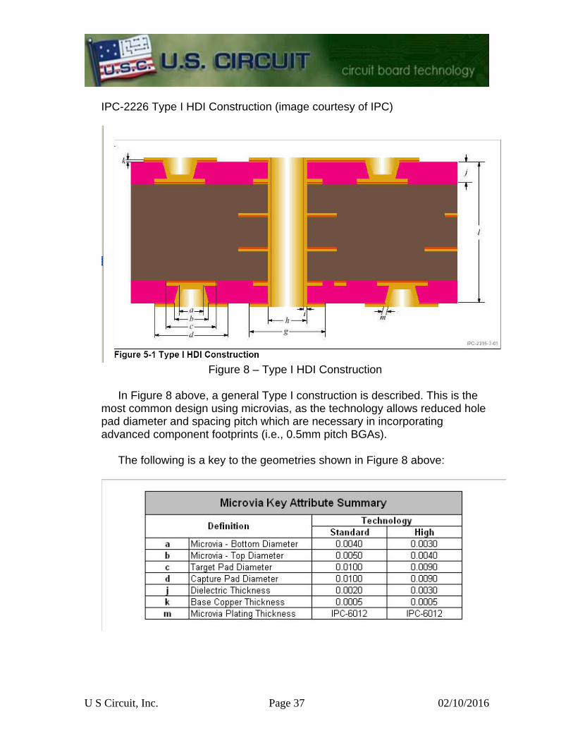
IPC-2226 Type I HDI Construction (image courtesy of IPC)
Figure 8 – Type I HDI Construction
In Figure 8 above, a general Type I construction is described. This is the most common design using microvias, as the technology allows reduced hole pad diameter and spacing pitch which are necessary in incorporating advanced component footprints (i.e., 0.5mm pitch BGAs). The following is a key to the geometries shown in Figure 8 above:

U S Circuit, Inc. Page 38 02/10/2016
If the board has fine pitch BGAs or other components, the microvia
technology allows the signal routing to drop down to the next internal layer thus avoiding extreme densities and trace width reductions on the plated surface layers (print & etch processing on inner layers can accommodate finer lines/spaces as compared to plated layers).
In the following image, a Type II construction is presented. The difference
here is that the addition of internal buried vias allow more advanced interconnect opportunities. Although it is not depicted in the image, microvias may be stacked on top of the buried vias if the appropriate processing is incorporated.
Figure 9 – Type II HDI Construction
If the area represented in the blue color (inside the buried via hole barrel)
is plated and then filled with a non-conductive epoxy the surface pads (layer 2 and n-1 in this image) may be plated over and then accommodate a direct stacked microvia laser ablated from layer 1 and layer n. For reference, the buried via on the left in the image represents partial filling from the surrounding prepreg (between layers 1 and 2 and layers n and n-1). This structure cannot accommodate a stacked microvia—they must be filled and plated over prior to outer layer lamination.
U S Circuit, Inc. Page 39 02/10/2016
Microvia in Pad This technology allows direct connection to the interconnect structure thus
saving valuable board real estate and provides advance signal routing opportunities. In order for the microvias to provide a flat, planar mounting surface for the component they must be filled and plated over much like the buried mechanically drilled vias. There are two methods of achieving this—copper filled microvias or epoxy filled and plated over microvias (USC currently builds epoxy filled microvias). Both structures allow a flat surface on top of the microvia which will prevent air entrapment during solderpaste stenciling and subsequent assembly. Gas entrapment is potentially harmful to ball-grid type components as the entrapped air can be ejected into the hollow ball of the device and then outgass during assembly, which results in a void on the ball’s surface. Filling the microvias is an additional process that will require additional lead time for manufacturing. Therefore, unless the microvias are designed specifically for via-in-pad technology, filling and plating over is not recommended. We will provide additional information on microvia technology in future revisions of this document. In the interim, a valuable resource is IPC’s standard for HDI designs IPC-2226. An excellent reference and history of microvia development can be found in Happy Holden’s HDI Handbook, available free of charge in .pdf format on the PCB007 website.

U S Circuit, Inc. Page 40 02/10/2016
U.S. Circuit, Inc. Contact Information
Customer Service Rupal Sojitra (760) 489-1413 x 130 [email protected] Engineering & ECAM Mike Fariba (760) 489-1413 x 108 [email protected] Tarun Chavda (760) 489-1413 x 118 [email protected] Rupal Sojitra (760) 489-1413 x 130 [email protected]