university of virginia · jeol 6700 cold-field emission gun high resolution sem provides for both...
TRANSCRIPT

Equipment and Other Resources
1. Sample Preparation and Optical Metallography: sectioning, mounting, grinding and polishing. High speed abrasive saw and automatic polishers improve productivity. Beuhler Isomet 100 for sample sectioning, Simplimet 1000 for sample mounting, Phoenix 4000 automatic grinder/polisher.
Nikon Epiphot Inverted Microscope – equipped with SONY DFW-X7000 high resolution color CCD camera and Clemex Vision Lite 3.5 Image analysis software. Panasonic AG-5700 VCR as well as NEC NX18AS CCD Camera. HIROX KH 7700 Digital Microscope - Magnification Range: 0-7000x (optical), integrated illumination system, automatic calibration, 2D & 3D measurement analysis and image tiling, dynamic image focus for rough surfaces, still image and video recording, 3D rotation during live imaging, large depth of field.
TEM Disc preparation –ultrasonic cutter and mechanical punches; Fishione and VCR dimplers. Electropolishing equipment – Struer’s Tenupol 3 and Fischione units. Gatan Precision Ion Polishing thinning non-metallic samples / cleaning of electropolished samples. FEI 200 Focused Ion Beam (FIB) – 30kV liquid Ga ion source, min. spot size <10nm. Secondary Electron (SE) imaging, Scanning Ion Microscopy, Mass Spectrometry.
2. Scanning Electron Microscopy: JEOL JXA-840A SEM provides conventional scanning electron microscopy and microanalysis. Energy Dispersive Spectroscopy (EDS), Secondary and Backscattered Electron Imaging, Electron Backscattered Patterns, as well as extensive recent upgrades including stage automation, digital image storing, and image processing. HKL Technologies NL1 - digital CCD for high speed/high sensitivity EBSD pattern collection. HKL Technologies Channel-5 EBSD Software – package for rapid data collection, pattern indexing, and microtexture data analysis and imaging (including orientation image maps, pole figures, inverse pole figures, orientation/misorientation distributions.) JEOL 6700 Cold-field emission gun High Resolution SEM provides for both high resolution scanning electron microscopy and microanalysis. Energy Dispersive Spectroscopy (EDS), Secondary and Backscattered Electron Imaging, and Cathodoluminescence Spectroscopy and Mapping.
3. Transmission Electron Microscopy: FIE TITAN – Schottky field emmision gun analytical electron microscope (80 - 300kV S-TWIN platform), provides high resolution STEM: 0.135 nm and TEM: 0.205 nm imaging. EDAX – EDS and Electron Energy Loss Spectrometry (EELS) along with Gatan Model 863P Tridiem GIF and HAADF detection. Gatan 794 Mult-scan Camera (EFTEM). Accessories include cold stage, low background, double-tilt specimen stage. JEOL JEM 2000FX – is equipped for high specmen tilt so that diffraction contrast experiments can be performed. A thin window EDS detector permits X-ray chemical analysis. This microscope is equipped with both a Gatan image intensifying TV and slow-scan CCD cameras. Current specimen holders provide capabilities for high-angle double-tilting, heating, EDS analysis, and straining.
4. X-ray diffraction (XRD) facilities: Panalytical X’pert MPD – computer-automated powder diffractometer equipped with pre-Fixed optics for easily transition from focusing to parallel beam optics. Also equipped with the X’cellerator detector for rapid data collection in focusing mode and a multi-sample sample stage. Rigaku Smartlab - state of the art in fully automated modular XRD systems (Winner of the 2006 R&D 100 Award for technical innovation). This high-resolution diffractometer incorporates a high resolution theta/theta closed loop goniometer drive system, cross-beam optics (for focusing and parallel beams), 4-circle goniometer for performing texture, residual stress, thin film, reflectometetry, a high temperature stage, and in-plane scattering arm for measuring ultrathin-films (few monolayers). JADE software and ICDD PDF4 database – for data analysis and
University of Virginia

phase identification. popLA (preferred orientation package of Los Alamos) software - used to analyze texture data generated using x-ray (or neutron) diffraction.
5. Mechanical Testing Facilities include an Instron servohydraulic and a MTS screw-driven universal testing system, both with 50 kN load capacities. The instruments are computer controlled and facilities exist for cryogenic and high temperature (450C max ATS furnace and miniature 1400C max MTS furnace) testing in air. Specialized grips and extensometry exists for tensile, compressive, fatigue, transverse (for Poisson ratio and r-value measurements) and high temperature testing.
Instron Custom Torsion test system with 1200 RPM at 22 Nm (200 lbf-in) capacity consisting of a torsion reaction frame with high rotational stiffness and 5500 digital control system and data acquisition electronics. Axial/Torsion load cell to measure torque and axial load on the specimen with 500 lbf tension and comression axial and 200 lbf-in CW and CCW torque capacities. 2 Vortec cooling guns with magnetic bases for cooling of sample fixturing during high temperature testing. High temperature capability provided by a Quad-4 infrared (optical) furnace. The laboratory also contains a suite of atmospheric creep testing load frames with temperature capability to up to 400ºC.
MTS Nanoindenter - fully programmable load and displacement histories and a positioning resolution of nanometers. The multiple indenter heads permit load range spans from 1 nN to 20 kN. The displacement resolution of the indenter to be acquired is less than 0.01 nm. The loading rate can be varied from 1 mN/sec to over 70 GN/sec. This equipment will be installed in a variable temperature environmental chamber capable of testing from -50°C to 100°C. A special nanoscale positioning stage is included for probing local variations in properties.
Environmental Fracture Laboratory for studies of environmental effects on fatigue and fracture. This facility contains 5 servo-hydraulic test machines manufactured by MTS and 1 Instron servo-electric machine; each is computer-automated by Test-Star IIS and Fracture Technology Associates data acquisition &analysis software. Each system includes both unloading compliance and direct current electrical potential difference instrumentation for crack length monitoring. Each machine is coupled with 1 or more environmental chambers, including those for water vapor saturated air and various electrolytes with potentiostatic control. One test machine is coupled with a ultrahigh vacuum system capable of establishing residual pressures of less than 200 nPa, while enabling full fracture mechanics experimentation. This oil-free vacuum system is copper gasket and metal bellows sealed, and coupled with a gas delivery system and quadrapole mass spectrometer for experiments in controlled pure-gas environments including water vapor, H2 and O2.

Georgia Tech Research Corporation
Equipment list
Tensile compression machine 200kN with liquid nitrogen set-up Mini compression stage for thin samples Philips X Ray Diffraction Scanning electron microscope Transmission electron microscope High performance cluster 64 nodes High performance cluster 256 nodes (Xeon processors)

FACILITIES AND EQUIPMENT
The following lab spaces are available for this proposed work. The central facility for conducting this work is at Nathan S. Swami’s Electrokinetic signal transduction lab that was constructed from university start-up funds. Other shared facilities accessible to the students include the Keck Imaging Center for Fluoresence Microscopy, the Microelectronics Fabrication Clean room and the analytical resources in the department of Chemistry.
Electrokinetic Signal TransductionOptical set-up: Bio-particle trapping under electrical and magnetic stimulation can be followed through the adjoining set-up on a Carl-Zeiss inverted microscopy system. The micro/nanofluidic channels and constrictions fabricated on quartz substrate is bonded to a cover slip and placed on the sample stage so that the electrical leads are accessible from the top. White light source from the top for phase contrast microscopy and laser, as well as Mercury-arc sources for bottom-illumination are available for fluorescence microscopy with manual filter change systems. Various high-magnification (63x oil immersion phase contrast) and low magnification (20x and 40x) objectives coupled to Hammatsu EMCCD (Electron Multiplier CCD) and PMT (Photo-multiplier tube) are available for imaging and spectroscopic analysis. An upright Zeiss microscope is also available for visual examination of samples. Electrical set-up: The electrical stimulation source consists of a National Instruments chasis with a number of waveform generators up to 20 Vp-p and 20 MHz frequencies, a A/D converter with a lock-in amplifier for signal acquisition and a microprocessor for on-chasis signal manipulation. A power amplifier for amplification up to 300 Vpp at 1 MHz is also available. Electrochemical set-up: Electrochemical analysis can be performed in parallel with electrical stimulation and optical imaging using the following systems:
Solartron moduLAB for potentiometry and impedance analysis: <http://www.solartronanalytical.com/Brochures/ModuLabBrochureA4.pdf>CH Instruments Scanning Electrochemical Microscope: <http://www.chinstruments.com/CHI900C%20SECM.pdf>A custom electrochemical cell is available that can hold microfabricated electrode tools and is driven by very fast electronics, capable to generate pulses down to 10-9 s.
Electron Microscopy and Scanning Probe MicroscopyOne scanning electron microscope (SEM) and one field emission SEM equipped with energy dispersive spectroscopy (EDS) for elemental analysis and electron backscatter diffraction (EBSD) for phase identification and crystalline structure orientation Two transmission electron microscopes, one with atomic resolution, another equipped with an EDS system with <1 nm resolution
Figure 1: Set-up for imaging electrokinetic manipulation in micro/nanofluidic devices.
JEOL 8600 electron probe microanalyzer (EPMA) Optical light microscopes Sample preparation facilities (metallographic polishing equipment, diamond saw, TEM disc cutter, Focused Ion Beam Milling) Perkin-Elmer PHI 560 XPS/scanning Auger system Molecular Imaging Electrochemical AFM/STM for imaging down to atomic resolution ex-situ and in electrolytes
Structural CharacterizationLow and high-angle X-ray diffractometers
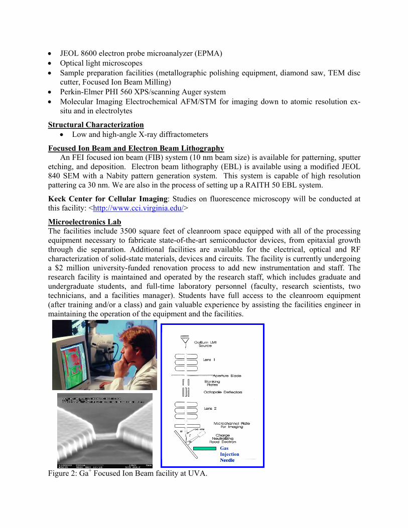
Focused Ion Beam and Electron Beam LithographyAn FEI focused ion beam (FIB) system (10 nm beam size) is available for patterning, sputter
etching, and deposition. Electron beam lithography (EBL) is available using a modified JEOL 840 SEM with a Nabity pattern generation system. This system is capable of high resolution pattering ca 30 nm. We are also in the process of setting up a RAITH 50 EBL system.
Keck Center for Cellular Imaging: Studies on fluorescence microscopy will be conducted at this facility: <http://www.cci.virginia.edu/>
Microelectronics LabThe facilities include 3500 square feet of cleanroom space equipped with all of the processing equipment necessary to fabricate state-of-the-art semiconductor devices, from epitaxial growth through die separation. Additional facilities are available for the electrical, optical and RF characterization of solid-state materials, devices and circuits. The facility is currently undergoing a $2 million university-funded renovation process to add new instrumentation and staff. The research facility is maintained and operated by the research staff, which includes graduate and undergraduate students, and full-time laboratory personnel (faculty, research scientists, two technicians, and a facilities manager). Students have full access to the cleanroom equipment (after training and/or a class) and gain valuable experience by assisting the facilities engineer in maintaining the operation of the equipment and the facilities.
Figure 2: Ga+ Focused Ion Beam facility at UVA.
Gas Injection Needle
Gas Injection Needle

A dual growth chamber, 6” substrate, MBE system is available; the introduction chamber includes a 30 nm resolution FIB patterning system. The world prototype of the "SCALPEL" projection electron lithography system is also available. The prototype SCALPEL Proof-of-Lithography system (SPOL) uses 100 keV electrons to expose 1/4 x 1/4 mm fields at a resolution of 80 nm typically. We also have access to an SEM-based electron beam direct writing system, which is capable of sub-100nm resolution. These prototyping tools will be used for the research described in this proposal. Fabrication processes developed with the serial direct-write electron-beam system are directly extensible and scalable to projection electron beam lithography using the SCALPEL SPOL system or ultimately, commercially available systems. Other instrumentation includes: Zeiss field emission SEM; UV and deep UV contact photolithography with submicron alignment (plus two sub-micron Nikon steppers waiting to be installed); ultra high vacuum RF sputtering systems for insulators and metals; ultra high vacuum DC magnetron sputtering of aluminum and niobium; plasma and reactive ion etching (both chlorine and fluorine based); thermal and electron-beam evaporation of metals and insulators; ion milling, oxidation, diffusion, and electrochemical plating and etching. Two high-speed dicing saws, two leak detectors, a computer controlled surface profiler and a wirebonder are also available.
Tip-enhanced Raman spectroscopy: Inaddition to the description in the proposal, following is a schematic of the tip enhanced Raman technique that we are developing to construct “Raman maps” of small device areas (~50 nm).
Nanotechnology Building: The electrokinetics lab of N. Swami is housed in University of Virginia’s Nanotechnology building, which has 40,000 square feet of gross space (Figure 4).
Figure 3: Tip-enhanced local Raman spectroscopy.
Figure 4: Materials Science and Nanotechnology Building

1
University of Virginia Laboratory Facilities and Measurement Capabilities
FAR-INFRARED RECEIVER LABORATORY The Far-Infrared Receiver Laboratory occupies a 3000 square-foot facility in the Physics Department at the University of Virginia and, over the past 20 years, has focused on the design, fabrication, assembly, and testing of components operating throughout the millimeter and submillimeter wave range, from 100 GHz to 3 THz. Research in this laboratory has concentrated on fundamental components such as frequency multipliers, sideband generators, detectors, and mixers based on semiconductor (particularly Schottky barrier diodes) and superconducting devices (including SIS tunnel junctions and hot electron bolometers). In addition, the laboratory has significant expertise in millimeter/submillimeter-wave metrology, including s-parameter characterization, power/frequency measurements, wafer probing, antenna pattern mapping, and terahertz spectroscopy.
Figure 1. Images from the Far-Infrared Receiver Laboratory. Left: optical bench for testing/characterizing sideband generators. Right: far-infrared molecular gas laser. The FIR laboratory is fully equipped for the design, assembly and evaluation of THz wavelength components and houses a wide variety of equipment for RF/millimeter/submillimeter-wave testing and characterization. This includes an HP 8510C vector network analyzer, HP 8720 network analyzer, a Rhode and Schwarz ZVA40 four-port network analyzer, a number of frequency synthesizers operating to 50 GHz, spectrum analyzers (HP 8565 and 8593), power meters (HP and Erickson), microwave and RF amplifiers, lock-in amplifiers, digital multimeters, power supplies, high quality optical tables, a Martin-Puplett diplexer, a Mach-Zehnder diplexer, a large collection of precision optical mounts, stages and positioners, and a variety of other antennas, frequency meters, and passive waveguide/coaxial components. For computation and modeling, the laboratory has a number of high-performance computers and software packages including Ansoft’s High Frequency Structure Simulator and Agilent’s Advanced Design System. For circuit assembly and testing, three wirebonders, several high-end stereo-microscope stations with micromanipulators and probes for assembling and testing devices and microcircuits, a number of stations for soldering, and a probe station for millimeter-wave s-parameter measurements are available. Moreover, the laboratory has recently acquired a cryogenic 67 GHz RF probe station for wafer probing down to temperatures of 1.7 K. The laboratory houses a number of specialized instruments for submillimeter measurement, including a Fourier Transform Infrared Spectrometer (FTIR), millimeter and submillimeter-wave frequency multiplier sources (operating to 1.6 THz), Schottky diode mixers and cryogenic bolometers, optical components,

2
and CO2-pumped molecular gas lasers suitable for use in the 500 GHz to 3 THz range. A variety of specialized solid-state sources, detectors, and spectroscopic instruments manufactured by Virginia Diodes, Inc. and covering the frequency range from 270 GHz to 1.6 THz are also housed and available in the laboratory. Additional facilities include a number of liquid-He dewars and a closed-cycle He refrigerator for testing and characterizing cryogenic devices and circuits. MICROFABRICATION LABORATORY The University of Virginia Microfabrication Laboratory (see the UVML website at http://www.ece.virginia.edu/UVML/) resides within the Department of Electrical and Computer Engineering. This laboratory consists of 6,000 square feet of device fabrication facilities, of which roughly two-thirds is clean room space.
Figure 2. Images from the MicroFabriation Laboratory. Left: Oxford ICP DRIE chlorine etching tool used for diode fabrication. Right: deep-UV mask aligner with backside alignment. The UVML fabrication facilities are fully equipped for the fabrication of complex circuits and micromachined structures. Deposition tools include: a KJL HV loadlocked four DC/RF magnetron sputtering system with heated stage and in-situ cleaning for sputtering of a multitude of materials, a UHV load-locked DC magnetron superconductor sputtering system for deposition of Al (for the formation of AlOx and AlN tunnel barriers), Nb, NbTiN and Au with in-situ cleaning, an HV load-locked DC/RF magnetron sputtering tool for the sputtering of Ti, Nb, Au and PdAu (1-15 Ω/square resistors) with in-situ ion cleaning, two single target RF diode sputtering systems and a new AJA Inc dual chamber UHV ten magnetron gun sputtering tool with 900C heated and cold stage will arrive before the end of the year. Two new CHA six crucible E-beam Evaporators with integral ion cleaning and dual liftoff/edge coverage wafer fixturing have also been recently added to the laboratory. Dry etching tools include two fluorine based reactive ion etchers, a TRION fluorine based Inductively Coupled Plasma (ICP) deep reactive ion etcher (DRIE), and a new Oxford Instruments chlorine based ICP DRIE with a temperature controlled stage (-150 to 400C) with laser endpoint detection. Mask aligners include an MJB3 and a new MJB4 Karl Suss aligner at 320nm, a EV620 320nm tool with true backside alignment and a joint Department of Materials Science (MS) and ECE E-beam lithography tool for 150nm dimensions. Diagnostic equipment includes a Veeco Dektak-8 surface and stress profiler, a Veeco NT-100

3
Optical Profiler, an FSM laser based thin film stress measurement system, a new Horiba Jobin Yvon UVISEL phase modulated spectroscopic Ellipsometer, a new Zeiss Supra 40 FESEM with STEM and an Inca 250 EDX microanalysis package, a joint ECE MS Phillips Analytical xray diffraction system, and a room temperature and a Desert Cryogenic (to 4.2K) probe station. Additional equipment includes a new Logitech PM5 auto-pol precision Lapping & Polishing Machine and a Disco DAD-2H/6T dicing saw.
MILLIMETER-WAVE MEASUREMENT LABORATORY
The Millimeter-Wave Measurement Laboratory resides within the Department of Electrical and Computer Engineering and has facilities for the design, testing and assembly of millimeter and submillimeter-wave circuits and systems. This laboratory is fully equipped to design, assemble and evaluate millimeter and submillimeter-wave mixers, multipliers and receivers and houses a variety of microwave and millimeter-wave equipment for RF testing and characterization. This includes three vector network analyzers (an HP8510C operating up to 325 GHz, an HP8720C operating to 20 GHz, and an HP8753 operating to 3 GHz). The laboratory also houses a variety of millimeter-wave synthesizers (Systron-Donner and Agilent) operating to 50 GHz, spectrum analyzers (HP 8593), power meters (HP 437B) with sensors up to 50 GHz, and a variety of antennas, RF amplifiers, frequency meters, and waveguide and coaxial components. For computation and modeling, the laboratory has a number of high-performance computers and software packages including Ansoft’s High Frequency Structure Simulator, Agilent’s Advanced Design System, and Agilent’s Momentum. For circuit assembly and testing, two wirebonders, a eutectic dye bonder, a number of stations for soldering and assembling planar circuits, and a Karl-Suss probe station for millimeter-wave S-parameter measurements are available.
Figure 3. Images from the Millimeter-Wave Measurement Laboratory. Left: HP 8510C vector network analyzer with OML, Inc. extension modules. Right: Rhode and Schwarz ZVA40 four-port vector network analyzer with extension unit from Virginia Diodes, Inc.
1
Facilities Statement Clinical: none Animal: none Computing: The Center maintains a computing space in the office dedicated for use by research assistants. The computing area has two Mac OS X desktop computers. There is also a scanner and laser printer. Office: The Center for Risk Management of Engineering Systems shares some facilities and administrative functions with the Department of Systems and Information Engineering. The Center has dedicated offices for the Director, Research Faculty, and Coordinator and Research Specialist, who will be involved in the proposed research. The Director’s office has a Polycom speakerphone for teleconferencing, Polycom video teleconferencing equipment and projection equipment that are used for brainstorming and discussion of research progress. Major Equipment: Large computing resources are maintained by the Information Technology and Communication (ITC) at the University of Virginia. A detailed list of available computing resources can be found in this website <http://www.itc.virginia.edu/labs/>. In addition the university maintains an extensive number of up-to-date software licenses, such as ArcGIS, MATLAB, MathCAD, and SAS, to name a few. The complete listing of available software can be found in <http://www.itc.virginia.edu/labs/listLibSoftware.php>. Laboratory: Phantom System Modeling Laboratory--PSML 1. Platform Development
a. Testbed Development A PSML testbed has been built with five Dell desktop PCs. We plan to upgrade to new computers in the near future. The specifications of the current desktop PCs are below: • CPU: Quad Core Intel Xeon 2.93GHz • Memory: 4GB • Hard Drive: 500GB • Network: 10/100/1000 Gigabit Ethernet Interface The structure of the testbed is shown in Figure 1, which provides a network connected distributed computing platform. A web server is developed on the front-end machine to provide web-based interface for users to configure, execute PSML simulation models, and view and analyze the execution results.

2
Figure 1. PSML Testbed Configuration
Currently the focus is on the development of component technologies, i.e., the multi-layer simulation models based on the needs of PSML.
b. Cloud Development An activity on developing cloud/SOA network platform has been carried out independently in PSML. A prototype cloud platform has been built using Open Source Eucalyptus Enterprise Edition Software. The cloud based Java communication, MySql database management and website technology have been tested.
2. Software Development a. Off-the-Shelf Software Installation
To fulfill the simulation tasks defined in PSML, the following software have been installed and used: • MatLab 2009 • SAS • SAP 2000 • Java • Eclipse • Ansys 12 • Apache and MySQL
b. Multi-layer Customized Software Development Two customized multi-layer simulation model have been developed: • Factor of Safety (FOS) Model. It uses weigh-in-motion data across the I-81 James River
Bridge to create the distribution of the Factor of Safety on the bridge. In the implementation, a web interface is provided for a user to specify the input data file. The input file is transmitted to the Modeler machine, on which Matlab, SAS and customized scripts execute the assigned tasks. Finally, the results are sent back to web interface to display.
• Computational IIM Solver. As the core module for the IIM analysis, it takes the formulated interdependency data and the input and produces output of inoperability and economic losses. Currently the single region Computational IIM Solver has been implemented. It provides a web interface for users to create or upload a demand/supply chain, upload intraregional sector interdependency matrix and nominal values. Once submitted, the task is fulfilled by Java IIM Solver implementation. The results are sent back to the web interface to display and analysis.
c. SOA Protocol Development

3
The SOA (Service Oriented Architecture) provides a flexible and efficient ways to provides solutions in the form of services. The following SOA protocols have been defined that consist of the following messages: • Service Descriptor • Service Registration • Service Update • Service Request • Service Reply
The SOA protocols are under implementation. Office (School of Medicine): Office space currently exists for all proposed personnel associated with this application. This office space for the physicians is present within the Division of Hematology and Oncology and the Division of Gastroenterology and Hepatology. Both Divisions are physically located within the West Complex of the University of Virginia Medical Center, and are in close proximity to each other, as well as to the Strickler Abdominal Transplant Clinic. The Medical campus is directly adjacent to the main grounds of the University of Virginia, allowing for walking access for easy face-to-face meetings with the Department of Systems Engineering personnel. Clinical: The Hepatoma Clinic at the University of Virginia is a highly integrated clinical program providing multi-disciplinary care to patients with hepatocellular carcinoma from throughout the mid-Atlantic region. The HCC program at UVA has increased its volumes by nearly 500% in the past decade, and now regularly draws patients from a population of 5 million lives encompassing Virginia, West Virginia, North Carolina, eastern Tennessee, and suburban DC and Maryland. The hepatoma program is fully integrated within the liver transplant program, being staffed by the same hepatologists who can seamlessly transition new referrals into the transplant program if indicated. The liver transplant program at UVA has become the largest volume transplant program between Philadelphia and Florida and UVA has performed more liver transplants annually than other any center in the region with the exception of Georgetown University. The transplant team at UVA consists of three transplant surgeons supporting both the living donor and deceased donor transplant programs and five transplant hepatologists (Drs. Carl Berg, Abdullah Al-Osaimi, Patrick Northup, Curtis Argo and Neeral Shah, two of whom are co-investigators on this grant application). The multi-disciplinary hepatoma tumor board at UVA meets weekly to review all HCC cases under management or that have been sent for referral, including those patients pursuing transplant as the desired therapeutic intervention. The robust tumor board involves participation by the liver transplant surgery team, the hepatobiliary surgery/surgical oncology group, the hepatology team Iincluding Drs. Berg and Northup), GI oncology (including Dr. Hanna Sanoff), radiation oncology and interventional radiology. The medical and surgical components of the hepatology program occupy dedicated, common inpatient space within the University of Virginia Medical Center. The hepatologists direct a dedicated inpatient Hepatology Service for all pre-transplant and hepatology oriented post- transplant admissions on 5 Central (sharing 30 inpatient beds with the inpatient GI service). Adjacent to this floor is the inpatient Abdominal Transplant service located on 5 West where all recent liver and kidney transplant patients are admitted. These two floors are adjacent to the Surgical ICU where all transplant ICU patients are cared for. This geographic proximity provides for seamless transition and consultation between the medical and surgical components of the transplant team, as well as comprehensive follow-up of all patients with hepatocellular carcinoma throughout their inpatient care. Five full time liver transplant nurse coordinators support the routine clinical care of liver transplant candidates and recipients in the outpatient setting while four full time nurse practioners further support
4
the inpatient liver transplant service. An additional three clinical nurse coordinators support the care of hepatoma patients for whom liver transplant is not considered an appropriate option. The University of Virginia is a fully computerized Medical Center with a fully integrated clinical computing system. The Epic computer system provides computerized access to all clinical events occurring within the Medical Center including procedure reports, anesthesiology records, outpatient visits by any provider, pathology results, and imaging. In addition, scanned records from all outside providers are incorporated into the computerized medical record. This HIPAA compliant, password protected comprehensive patient information system greatly facilitated retrospective collection of data. Epic is accessible by every desktop computer within the medical system, and by means of VPN access to laptops both on grounds and offsite. All of the medical faculty involved in the hepatoma program at UVA have Dell personal desktop PCs which are maintained by dedicated information technology support staff from the Department of Medicine.