university of potsdam · semiconducting polymers as the active component in ofets. first, the...
TRANSCRIPT

University of Potsdam Faculty of Mathematics and Natural Sciences Institute of Physics
Advanced Lab Course: Organic Field Effect Transistors 2
I. GOALS AND EXPERIMENTAL TASKS • Discussion and understanding of the principle of operation of field-effect transistors.
• Discussion and understanding of the mechanisms of conductivity and mobility in
polymeric semiconductors.
• Preparation and characterization of polymer-based field-effect transistors
• Determination of conductivity, mobility and on/off ratio of organic field-effect transistors
from output and transfer characteristic measurements.
• Effect of various preparation parameters (surface treatment, deposition of the active
polymer layer) and the transistor properties
• Influence of intentional and unintentional doping (with oxygen) on the transistor
properties.
• Discussion of the differences in mobility and on/off ratio of devices prepared by spin
coating and drop casting.

Advanced Lab Course: Organic Field Effect Transistors 3
II. INTRODUCTION The focus of this lab course is to understand the properties of thin film transistors (TFTs)
prepared from the semiconducting polymer polythiophene (PT). Thin film transistors belong
to the class of field-effect transistors (FETs), which are widely used as active components in
microprocessors, active matrix displays, chip-cards etc. All these transistors have in common
that the charge distribution within a so-called channel is modified by applying an electric field
to a gate electrode. As a consequence, the electric current through a FET can be controlled by
an electric bias, without the need for a control current as in bipolar transistors. Therefore,
FETs are often used for amplification and switching applications with very small control
power requirements.
Various types of device concepts and materials are used today. Most transistors today rely
on crystalline or amorphous layers of inorganic semiconductors (Si, GaAs). In particular,
doped crystalline layers of Si and GaAs possess extremely high charge carrier mobilities µ,
exceeding 1000 cm2/Vs at room temperature. In combination with a thin oxide gate insulator
and a metal gate electrode, these MOSFETs are the basis of today’s microprocessors.
Alternatively, amorphous Si layers deposited as ultrathin films on suitable substrates are used
for switching the pixels in active matrix displays. Those layers possess mobilities of the order
of 10-1 to 1 cm2/Vs. All Si-based transistors have the disadvantage that their preparation
requires high-temperature processing steps and that they can not be fabricated as flexible
large-area electronic devices.
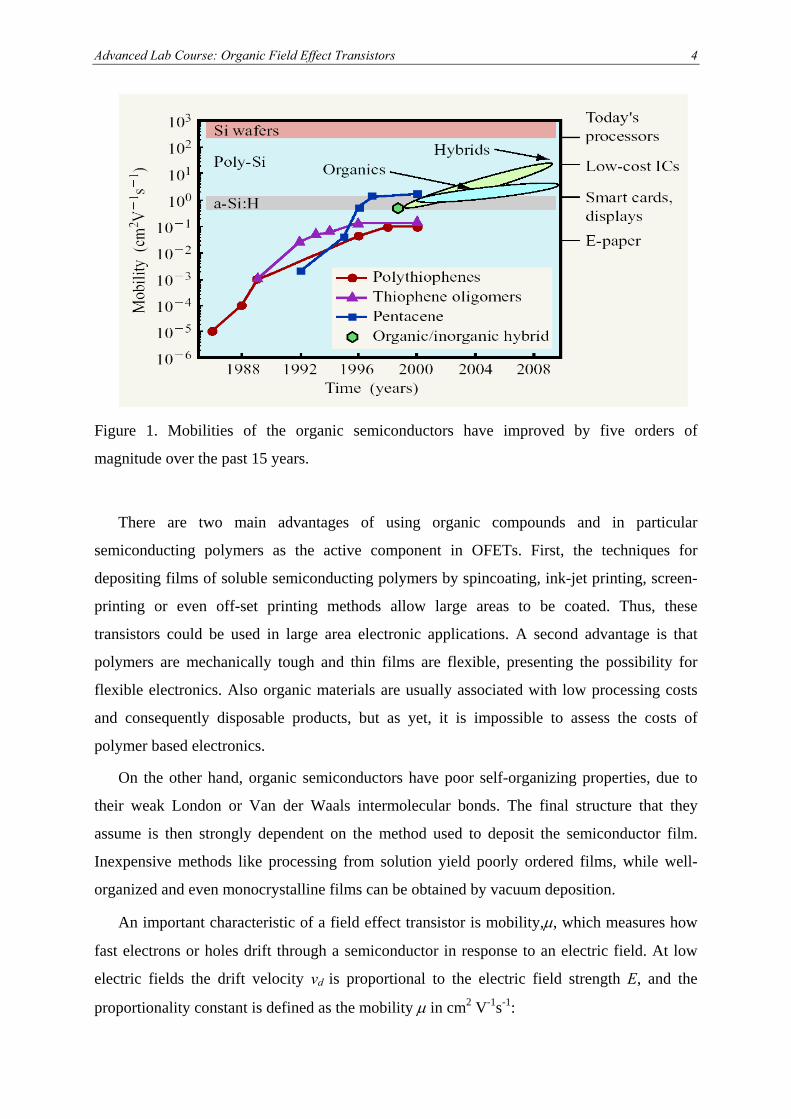
Organic field-effect transistors (OFETs) have been introduced in 1986. These first
OFETs utilized a semiconducting polymer, namely, polythiopene. However, in this pioneer
work, a low carrier mobility of only ∼10-5 cm2/Vs was reported. Since then, the performance
of field effect transistors based on organic materials has continuously improved, as shown in
figure 1, approaching the performance of transistors made from a-Si:H.
Advanced Lab Course: Organic Field Effect Transistors 4
Figure 1. Mobilities of the organic semiconductors have improved by five orders of
magnitude over the past 15 years.
There are two main advantages of using organic compounds and in particular
semiconducting polymers as the active component in OFETs. First, the techniques for
depositing films of soluble semiconducting polymers by spincoating, ink-jet printing, screen-
printing or even off-set printing methods allow large areas to be coated. Thus, these
transistors could be used in large area electronic applications. A second advantage is that
polymers are mechanically tough and thin films are flexible, presenting the possibility for
flexible electronics. Also organic materials are usually associated with low processing costs
and consequently disposable products, but as yet, it is impossible to assess the costs of
polymer based electronics.
On the other hand, organic semiconductors have poor self-organizing properties, due to
their weak London or Van der Waals intermolecular bonds. The final structure that they
assume is then strongly dependent on the method used to deposit the semiconductor film.
Inexpensive methods like processing from solution yield poorly ordered films, while well-
organized and even monocrystalline films can be obtained by vacuum deposition.
An important characteristic of a field effect transistor is mobility,µ, which measures how
fast electrons or holes drift through a semiconductor in response to an electric field. At low
electric fields the drift velocity vd is proportional to the electric field strength E, and the
proportionality constant is defined as the mobility µ in cm2 V-1s-1:

Advanced Lab Course: Organic Field Effect Transistors 5
Evd =µ (1)
The mobility is further related to the conductivity σ through the density of charge carriers n
and the electron charge e:
en σµ = (2)
A second important parameter is the on/off ratio of the transistor, defined as the ratio of
currents in the on- and off-state (see below).
Efforts to increase the mobility can be done either by improving the process used for the
fabrication of the transistors or by synthesizing new organic materials. However, for transistor
applications of conjugated polymers, two main difficulties have to be overcome. The
disordered, amorphous morphology of most solution-processed polymer typically results in
low charge carrier mobilities. Polymers are also difficult to purify and residual extrinsic
doping often results in a high intrinsic conductivity, limiting the transistor on/off current ratio.
In the following chapters, the principle function and characteristics of thin film transistors
well be presented. Then, the charge transport in organic materials will be discussed, including
the interplay between layer morphology and field-effect mobility. In the Appendix, equations
describing the accumulation and transport of charges in a FET-structure are derived.

Advanced Lab Course: Organic Field Effect Transistors 6
III. THE FIELD EFFECT TRANSISTOR
III.A. Working Principle
Figure 2 shows the general structure of a thin-film transistor.1 It consists of an undoped
charge transporting layer, the organic semiconductor, in direct contact to two electrodes, the
source- and the drain electrodes. Further, there is a third electrode, the gate electrode,
separated from the semiconductor by a thin gate-insulator. Thus, a thin-film transistor can be
considered as a parallel-plate capacitor, where one plate is constituted by the gate electrode
and the other one by the semiconducting film. The semiconductor between the source and the
drain below the gate electrode forms the so-called channel, defined by the channel width W
and the channel length L.
LW
Substrate
Semiconductor
Gate -Isolator
Source - and drain electrodes
Gate -electrode
LW
Substrate
Semiconductor
Gate -Isolator
Source - and drain electrodes
Gate -electrode
Figure 2. A thin-film transistor in the top-gate geometry
When a gate voltage VGS is applied between the gate and the source, majority carriers
accumulate at the insulator-semiconductor interface, leading to the formation of a conducting
channel between source and drain (Figure 3). In most organic semiconductors, holes are the
mobile charges, so a negative bias has to be applied to the gate. A second bias VDS applied
between source and drain then produces a drain current (ID). For the case that GSDS VV < ,
this drain current is given by:1,2
VV C L
W I DSGSiD µ= (3)
Here, Ci is the capacitance of the gate insulator per unit area, defined by:
iii dC εε 0= (4)

Advanced Lab Course: Organic Field Effect Transistors 7
with εi and di the permittivity and the thickness of the gate insulator, respectively. Note that in
this regime, the drain current ID increases strictly linear with the bias applied to the gate. This
is due to the fact that with increasing gate bias, the number of charges accumulated at the
insulator/semiconductor interface increases linearly with VGS (see Appendix).
SemiconductorS D
Gate Isolator
G+-
-+
VDS
VGS
+ + + + + + + +SemiconductorSS DD
Gate Isolator
G+-
-+
VDS
VGS
+ + + + + + + +
Figure 3. Schematic view of an organic field effect transistor (p-type). When a negative bias VGS is applied between the gate electrode and the source contact, negative charges accumulate at the gate/insulator interface. As in an ordinary capacitor, a sufficiently strong electric field across the insulator thereupon induces charges of opposite sign (holes) along the insulator/semiconductor interface, if the semiconducting material is p-type. These holes form a conducting field-effect transistor channel between the source and drain. A second bias VDS applied between source and drain produces a current (ID) whose magnitude depends crucially on the carrier mobility µ, the gate bias VGS and the drain voltage VDS.
Two important technological parameters are the so-called channel conductance Cc and the
transconductance Tr, relating the current flowing between source and drain to the voltage
applied to the drain and gate contact. For the case that GSDS VV < , these are given by
equation 5 and 6, respectively:
constant DS
D
GS
GSiV
c VCL
WVIC µ=
∂∂
==
(5)
constant GS
D
DS
DSiV
r VCL
WVIT µ=
∂∂
==
(6)
If the voltage VDS applied between drain and source becomes comparable to voltage VGS
between gate and source, the density of charges accumulated in the semiconducting layer

Advanced Lab Course: Organic Field Effect Transistors 8
close to the drain contact decreases due to charge repulsion. For GSDS VV = , no charges will
accumulate close to the drain contact. This defines the onset of current saturation. For
GSDS VV > , in the saturation regime, the drain current and transconductance are given by
Equation 7 and 8, respectively:
V C L
W I 2GSisaturationD, µ
2= (7)
VC L
W T GSir µ= (8)
The complete derivations of the equations are given in the appendix.
Typical output characteristics are shown in figure 4 (upper graph). In this characteristic,
the drain current is measured as a function of the source-drain voltage at a constant gate
voltage. There are two distinct regimes: firstly, the linear regime according to Equation 3 is
observed at low source-drain voltages, the drain current increases linearly as the source-drain
voltage increases. In this regime the charge density in the conducting channel is relatively
uniform. Secondly, the saturation regime is observed at VDS > VGS, where the total charge
density in the conducting channel decreases (Equation 7) and the current becomes
independent of drain bias.
Also shown in figure 4 is a typical transfer characteristic of an organic field effect
transistors. Here, the drain current is measured as a function of the gate voltage at a constant
source-drain voltage. From this characteristic, the on/off ratio of the device, defined as the
current at maximum gate bias divided by the current at zero or even positive gate bias, can be
deduced as an important transistor property. Note, that in the off-state, no charges are
accumulated by the gate; all charges present in the layer under these conditions must be
"intrinsic" charges, caused by e.g. doping or impurities. In this case, the drain current is
simply given by:
DSse
D VLWd
Iσ
= (9)
Here, σe is the conductivity of the semiconductor and ds is the thickness of the semiconductor
layer. For high on-off ratios; this current must be as small as possible. Therefore, thin
semiconducting layers with small intrinsic conductivities are needed.

Advanced Lab Course: Organic Field Effect Transistors 9
Drain C
urrent ID (A
) D
rain Current ID (A
)Figure 4. Typical output characteristics (ID as a function of VDS for fixed values of VGS) and transfer characteristic (ID as a function of VGS for fixed values of VDS) in the saturation regime of a poly(thienylene vinylene) transistor3.
III.B. Parameters and Material Requirements
Intrinsic conductivity
Various parameters control the performance of TFTs. First, in order to possess a low off-
current, the intrinsic conductivity must be as low as possible. As outlined below, intrinsic
organic semiconductors are almost insulating with a very low density of mobile charges.
However, dopands such as oxygen or other electron-donating or electron-accepting
compounds (such as in PEDT:PSS) can lead to a considerable density of free charge carriers
and, concurrently, to a large conductivity in the off-state.

Advanced Lab Course: Organic Field Effect Transistors 10
Interface properties
As shown in the Appendix, charges in the TFT active layer are accumulated very close to
the gate insulator. Therefore, the interface between the insulator and the organic
semiconductor as well as the morphology of the active layer adjacent to this interface controls
the charge transport in an OFET. If, e.g. the insulator consists of SiO2, dangling bonds at the
surface constitute electrical dipoles, which alter the local electronic transport properties of the
surrounding material. Hexamethyldisilazane (HMDS), octadecyltrichlorosilane (OTS) and
other moieties with reactive silane or alkylsilane end-groups have been used to passivate the
SiO2 surface. By chemical reaction, these compounds form a dense self-assembled monolayer
(SAM), yielding a well defined ordered surface for subsequent semiconductor deposition. In
this laboratory course, HMDS is used to provide the SAM (polydimethylsiloxane) on top of
SiO2. Note, that the silanisation (HMDS treatment on SiO2) is a slow multiple-step reaction.
The reaction mechanism and sequence during the silanisation process using HMDS is shown
in figure 5.
Figure 5. The reaction mechanism and sequence during silanisation process using Hexamethyldisilazane (HMDS).

Advanced Lab Course: Organic Field Effect Transistors 11
Mobility
Finally, the semiconductor should possess a sufficiently large mobility. Since organic
semiconductors constitute of individual molecules hold together mainly by van-der-Waals-
forces, with no electronic overlap between the orbitals of neighboring molecules, the hopping
of charges between the molecules is a major limiting step. This will be discussed in the
following.

Advanced Lab Course: Organic Field Effect Transistors 12
IV. ORGANIC MATERIALS FOR FIELD-EFFECT TRANSISTORS
IV.A. ORGANIC SEMICONDUCTORS Organic material can possess either p-type or n-type transport properties. In p-type
semiconductors the mobile carriers are holes, while in n-type the mobile carriers are
electrons. For various reasons, the most widely studied organic semiconductors are p-type,
examples of these are shown in figure 6.
1 2
4
5
6
7
3 4
Figure 6. Examples of p-type semiconductors for field effect transistor application: tetracene (1), pentacene (2), thiophene oligomers / sexithiophene (3), poly(3-hexylthiophene) (4), phthalocyanine (5), α, ω, dialkylanthradithiophene (6), and polyacetylene (7).
All organic semiconductors have in common, that they possess a π-electron conjugated
system, build by the spatial overlap of the pz orbitals of the individual C-atoms. As a
consequence, the atomic p-orbitals combine to molecular π-orbitals, which often extend over
the whole molecule (in case of small molecules) or over a large number of repeat units (as in
conjugated polymers). In the pristine (undoped state) a certain number of molecular orbitals
are completely occupied with electrons. The highest occupied molecular orbital is denoted as

Advanced Lab Course: Organic Field Effect Transistors 13
HOMO. Orbitals with even higher energies are (almost) completely empty; the lowest
unoccupied molecular orbital is called LUMO. In the bulk state, mobile electrons move by
hopping between LUMOs of neighboring molecules (and holes by hopping between the
HOMOs) as shown in figure 7. Therefore, the HOMO-energy translates into the energy of the
valence band, the LUMO-energy into the conduction band energy and the HOMO-LUMO-
distance corresponds to the semiconductor bandgap. In general, the HOMO-LUMO distance
is 2 – 4 eV and the material is a semiconductor with a very low intrinsic density of mobile
charge carriers.
Charge transport is relatively easy within a molecule, but due to the disordered molecular
structure of most organic semiconductors, charge transport between molecules is much more
difficult. A model that is often used to describe organic semiconductors to explain transport
between molecules (or more generally between localized states) is a thermally activated
charge carrier tunneling (hopping). The more ordered is the intermolecular structure, though,
the easier will be the hopping between molecules. This means that mobility will be better in
semiconductors that have a well organized structure.
unoccupied
occupied orbitals
LUMO HOMO
Figure 7. Scheme of the motion of charges between HOMOs and LUMOs of adjacent molecules (polymer segments) via charge carrier hopping.
Advanced Lab Course: Organic Field Effect Transistors 14
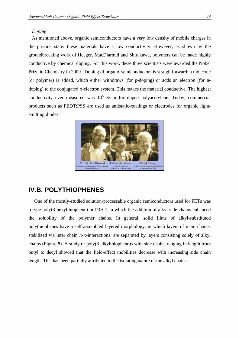
Doping As mentioned above, organic semiconductors have a very low density of mobile charges in
the pristine state: these materials have a low conductivity. However, as shown by the
groundbreaking work of Heeger, MacDiarmid and Shirakawa, polymers can be made highly
conductive by chemical doping. For this work, these three scientists were awarded the Nobel
Prize in Chemistry in 2000. Doping of organic semiconductors is straightforward: a molecule
(or polymer) is added, which either withdraws (for p-doping) or adds an electron (for n-
doping) to the conjugated π-electron system. This makes the material conductive. The highest
conductivity ever measured was 105 S/cm for doped polyacetylene. Today, commercial
products such as PEDT:PSS are used as antistatic-coatings or electrodes for organic light-
emitting diodes.
IV.B. POLYTHIOPHENES One of the mostly-studied solution-processable organic semiconductors used for FETs was
p-type poly(3-hexylthiophene) or P3HT, in which the addition of alkyl side-chains enhanced
the solubility of the polymer chains. In general, solid films of alkyl-substituted
polythiophenes have a self-assembled layered morphology, in which layers of main chains,
stabilized via inter chain π-π-interactions, are separated by layers consisting solely of alkyl
chains (Figure 8). A study of poly(3-alkylthiophene)s with side chains ranging in length from
butyl to decyl showed that the field-effect mobilities decrease with increasing side chain
length. This has been partially attributed to the isolating nature of the alkyl chains.

Advanced Lab Course: Organic Field Effect Transistors 15
Figure 8. Layered morphology of poly(3-alkylthiophene) in the bulk. Layers of conjugated main chains are separated by layers of isolating alkyl chains. Charge transports is fast along the conjugated electron system or by hopping between polymer chains within a main chain layer, but slow when carriers move perpendicular to the layers.
In fact, one expects that the packing and orientation of the conjugated main chains with
respect to the direction of charge transport plays a crucial role, since carriers can only move
along the conjugated electron system or by inter chain hopping between the conjugated
polymer backbones. The highest mobilities up to now of 0.05 to 0.1 cm2V-1s-1 were measured
for drop cast films of highly regioregular P3HT (consisting of 98.5% or more head-to-tail
(HT) linkages). In these drop cast films, the polymers self-organize into a well-ordered
lamellar structure with an edge-on orientation of the thiophenes rings relative to the substrate
(figure 9a). The edge-on lamellar structure ensures that delocalized intermolecular states are
formed in the direction parallel to the substrate, which is the transport direction in OFETs
devices.
The mobility of regioregular P3HT has been found to vary by two orders of magnitude
depending on the solvent used, with chloroform giving the highest mobility. Modification of
the substrate surface prior to deposition of regioregular poly(3-alkylthiophene) has also been
found to influence film morphology. For example, treatment of SiO2 with
hexamethyldisilazane (HMDS) or an alkyltrichlorosilane replaces the hydroxyl groups at the
SiO2 surface with methyl or alkyl groups. The apolar nature of these groups apparently
attracts the hexyl side chains of P3HT, favoring lamellae with an edge-on orientation.
Mobilities of 0.05 to 0.1 cm2V-1s-1 from highly regioregular P3HT have been attributed to this

Advanced Lab Course: Organic Field Effect Transistors 16
surface modification process.5 In constrast, the layers formed by P3HT with a less regular
structure tend to adopt an orientation perpendicular to the substrate plane. These layers
possess a much smaller mobility of the order of 10-3 cm2/Vs (figure 9b).
Figure 9. Two different orientations of ordered P3HT domains a, b, the wide-angle X-ray scattering images are colours representation of the two-dimensional distribution of scattered Cu Kα X-ray intensity from spin-coated, 70–100 nm thick P3HT films with regioregularity of 96% (a) and 81% (b) on SiO2/Si substrates. The vertical (horizontal) axes correspond to scattering normal (parallel) to the plane of the film. The insets show schematically the different orientations of the microcrystalline grains with respect to the substrate.4
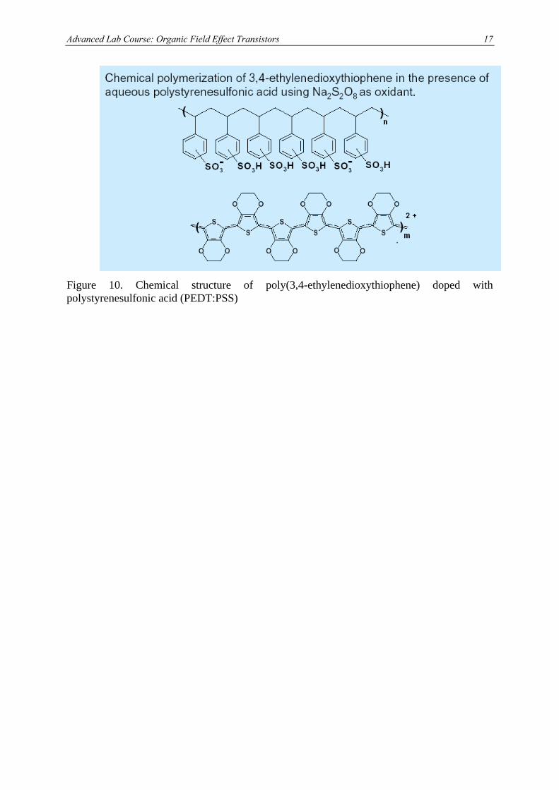
Doped polythiophenes
Polythiophene can be made conductive by doping. One commercially available product is
PEDT:PSS (see figure 10). Here, the dopand is a polyelectrolyte, polystyrenesulfonic acid.
Depending on the concentration of PSS, the material exhibits conductivities between 10-3 and
10 S/cm.
Alternative, exposure of poly(3-alkylthiophene) films to air causes an increase in
conductivity and a subsequent degradation of the transistor on/off ratio. This is caused by the
withdrawing of an electron from the conjugated system by oxygen (doping by water is a less
probable but possible cause), resulting in a p-doped polymer. This is one reason why good
transistor properties and high on/off ratios can be achieved only by preparing and testing the
devices in dry N2 atmosphere.
Advanced Lab Course: Organic Field Effect Transistors 17
Figure 10. Chemical structure of poly(3,4-ethylenedioxythiophene) doped with polystyrenesulfonic acid (PEDT:PSS)

Advanced Lab Course: Organic Field Effect Transistors 18
V. CHARGE TRANSPORT IN ORGANIC MATERIALS Hopping
In metals and conventional semiconductors, charge transport occurs in delocalized states. It is
limited by the scattering of the carriers mainly on phonons, that is, thermally induced lattice
deformations. Such a model is no longer valid in low conductivity materials such as
amorphous or organic semiconductors, where a simple estimate shows that the mean free path
of carriers would become comparable to the mean atomic distance. In these materials,
transport occurs by hopping of charges from one molecule to the next, between localized
states. A main difference between the delocalized and localized transport is that, in the
former, the transport is limited by phonon scattering, whereas in the latter, it is phonon
assisted.
Accordingly, the charge mobility decreases with temperature in conventional
semiconductors, the reverse being true in most organic materials. Several models have been
developed to rationalize the hopping transport. In most cases, the temperature dependence of
the mobility follows a law of the form µ = µo exp [- (T0/T)α], where α is either 1 or 2. The
case α = 1 represents the case of "conventional" thermal-activated transport, with the mobility
following an Arrhenius-type law. As a result, the mobility icreases strongly with increasing
temperature. At room temperature, the mobility in amorphous systems is well below 1 cm2V-
1s-1.
Field-Dependent Mobility
A general feature of charge transport in organic materials is that the mobility becomes field
dependent at high electric field (namely, at fields in excess of ~105 V/cm). This phenomenon
occurs through a Poole-Frenkel mechanism, in which the columbic potential near the
localized levels is modified by the applied field in such a way as to increase the tunnel
transfer rate between sites. The general dependence of the mobility is given by equation 10.
Here, µ(0) is the mobility at zero field, β = (e/πεε0)1/2 is the Poole-Frenkel factor, and F is the
magnitude of the electric field.
⎟⎠⎞
⎜⎝⎛= F
kTqF βµµ exp )0( )( (10)

Advanced Lab Course: Organic Field Effect Transistors 19
VI. EXPERIMENTAL AND DATA ANALYSIS
VI.1.1 Organic Field Effect Transistors from PEDT:PSS EXPERIMENTAL Preparing an organic field effect transistor using PEDT:PSS and measuring the output and
transfer characteristic.
TASK
1. Determine the conductivity from the device from the output measurement.
2. Do we have any transistor behavior from this device? Why?
3. How large is the on-off-ratio?
VI.1.2 Organic Field Effect Transistors from Poly(3-octylthiophene) (P3OT)
EXPERIMENTAL
Preparing an organic field effect transistor using poly(3-octylthiophene) (P3OT) using drop-
casting and spin-coating techniques.
TASK
1. Measure output and transfer characteristics of devices, which were prepared using
drop casting and spin coating of P3OT inside the glove box.
2. Determine the mobility from the linear region and also from saturation region of the
output characteristics measured inside the glove box.
3. Verify that equation A7 is correct. Calculate the charge carrier density profile n(y) in
the semiconductor for the experimental conditions. At which distance from the
insulator/semiconductor interface has the charge density dropped to ½ of the value
directly at the interface?

Advanced Lab Course: Organic Field Effect Transistors 20
4. Can you give an explanation why the mobility extracted from the linear and the
saturation regime give different values of µ?
5. Take out the samples from the glove box and measure output and transfer
characteristic of the devices under air.
6. Calculate the mobility from the linear region and also from saturation region for the
two devices measured outside the glove box. Explain the influence of oxygen on the
device performance.
7. Determine the on/off ratio for each device measured both inside and outside the glove
box.
The chemical structure of poly(3-octylthiophene) (P3OT)

Advanced Lab Course: Organic Field Effect Transistors 21
VII. APPENDIX6
In figure A1, the principle circuit of a transistor is shown. The source electrode is always
grounded; all the other voltages refer to this source electrode. A negative voltage applied to
the gate electrode will produce an accumulation of positive charges (holes) in the channel,
and the negative drain voltage will cause a drift of these charge carriers from source to drain.
DS
y
VG
S
Figure A1. Schem
Accumulation o
How do charg
gate electrode,
considered as a c
is formed by th
capacitor has a c
Here, 0ε is the pe
the insulator and
VG
atic illustra
f charges
es accumula
insulator an
apacitor, in
e semicond
apacity
rmittivity co
A is the „ac
VVD
tion of an OFET with all important parameters.7
te at the semiconductor/insulator interface? The combination of
d semiconductor (with source and drain electrodes) can be
which one plate is given by the gate electrode and the other plate
uctor between source and drain, the so-called channel. This
iii d
AC εε 0=′ . (A1)
nstant, iε is the permittivity of the insulator, di is the thickness of
tive“ area of the transistor, which is the product of channel length

Advanced Lab Course: Organic Field Effect Transistors 22
L and channel width W. For a transistor, one does not consider the capacity, but the capacity
per area:
i
ii d
C εε 0= . (A2)
By applying a voltage to the capacitor (later called the gate voltage, VGS), charge carriers will
be accumulated. The accumulated charge can be written as:
GSiVCQ ′= . (A3)
This assumes that the charge injection from the source electrode into the semiconductor
“plate” of the capacitor has no barrier. This plate of the capacitor is thus grounded. The
overall charge Q is a product of an elementary charge e, the number density of charge carrier
n and the volume in which the charge carriers are stored. In this model, it is assumed that the
charges accumulate over the full thickness of the semiconductor and not only at the
semiconductor/insulator interface. For the derivation of the transistor equation, this difference
is irrelevant. However, a detailed understanding of the charge transport properties requires
knowledge of the charge density distribution.
Assuming that no intrinsic charges are present, all charges in the active layer are injected
from the source- (and drain-) electrodes and attracted to the semiconductor/insulator interface
by the electric field caused by the charges on the gate electrode. In steady-state, the charge
density profile en(y) perpendicular to the interface is determined by
a) Poissons equation:
so
yendydE
εε)(
= (A4)
b) the condition that the drift current perpendicular to the interface (driven by the
superposition the field generated by the charges Q on the gate contact and the space charge
from the charges accumulated in the semiconductor) is equal and inverse to the diffusion
current:
0)()()( =−=+=dy
ydneDyEyenjjj diffdrifttotal µ (A5)
Here, εs is the permittivity of the semiconductor. With Einstein’s equation:
ekTD µ
= (A6)

Advanced Lab Course: Organic Field Effect Transistors 23
the following equation for the density profile and the electric field in the layer can be derived:
22 )(2)(
o
so
yyekTyn
+=
εε
)(
2)(oyye
kTyE+
−= (A7)
Here, y = 0 is at the semiconductor/insulator interface. Finally, the value of yo is determined
by the field at the interface:
GSiG
so UCA
QyE === )0(εε (A8)
Note that for a positive charge accumulation in the semiconductor, the charge on the gate
electrode QG and with that UGS must be negative! At reasonable fields and for typical
permittivities of organic semiconductors of the order of 3-5, most of the charge carriers
accumulate within few nanometers from the interface. In other words, only the transport
properties of the semiconducting layer in direct vicinity of the interface are relevant to the
transistor performance. Therefore, any defects at the surface of the insulator are detrimental to
good transistor performance.
Transistor characteristics
In the following, we assume that the charges are homogeneously distributed in the
semiconductor (in fact the concrete function form of n(y) is not relevant for the following
transistor equation). Therefore, we can rewrite equation A3 as the following
sGSi neWLdVC =′ (A9)
where ds is the thickness of the semiconductor.
Carriers that are accumulated in the channel will have the opposite sign with respect to the
gate voltage that is applied, e.g. for p-type semiconductors, when a negative voltage is applied
to the gate electrode, positive charges (holes) will be accumulated at the
semiconductor/insulator interface.
These excess carriers can be considered as free carriers. When a negative voltage is applied
to the drain, the accumulated holes will drift from source to drain, therefore, an ohmic current
will be generated:

Advanced Lab Course: Organic Field Effect Transistors 24
DSD Ej σ= (A10)
The drain current density jD is proportional to the electric field EDS between the source and
the drain, with the conductivity σ given by
µσ ne= (A11)
Here the mobility is not the bulk mobility but the FET mobility and contributions by intrinsiv
carriers are neglected. Note that, in a FET, the accumulation and transport of charges only
takes place at the interface between semiconducting material and insulator.
Rewriting equation A10 with the help of equations A9 and A11, we get
L
VWLd
VCj DS
s
GSiD ⋅⋅
′= µ (A12)
The product WL is the area of the capacitor from equation A1, therefore substitution of the
capacity by the capacity per area is possible. The drain current density is the drain current,
I
iC ′
D, over the cross sectional area of the semiconductor, which is given as the product of the
channel width W and the thickness of the semiconductor ds. Thus we can write equation A12
as the following:
DSGSi
D VVL
WCI ⋅⋅⋅= µ (A13)
The drain current is independent of the thickness of the semiconductor and it should increase
linearly with increasing drain and gate voltage. This is known as the field effect: The electrical
gate field, without or with only a small gate current will introduce a big alternation
(modification) of the drain current. This principle was used in triode tubes, where a centered
lattice is used onto which a control voltage can be applied. The current from electrons coming
from the (glowing) cathode to the anode can be controlled by this voltage.
MORE EXACT CONSIDERATION
In the previous derivation, the accumulation of charges is considered to be uniform over the
full channel length, as indicated in equation A3. Actually, a drain voltage is also required to
drive a current flow in the channel. It has the same sign as the gate voltage and reduces the
effective voltage drop in the drain region, which accumulates the charges in the
semiconductor. Thus, the accumulation is not uniform along the full channel length. The
accumulation in segment dx of the channel is dependent on the effective voltage at its
position. At the source, this is always the gate voltage since the source is always grounded. In

Advanced Lab Course: Organic Field Effect Transistors 25
contrast, at the drain electrode, the effective voltage is only the difference between the gate
and drain voltage. Within the channel, the effective voltage takes intermediate values
according to the so-called gradual-channel-approximation. We are assuming a linear decay of
the effective voltage V(x) from source to drain. This approximation works when the channel is
much longer than the thickness of the insulator and, therefore, the electric field along the
channel is smaller than the gate field, which is perpendicular to the channel. This assumption
is fulfilled in OFETs: the channel length is in the order of a few 10 µm, and the thickness of
the insulator is some 100 nm. With this assumption, the equation A13 can be written as
( ))( )( xVVVCxQ tGi −−′= (A14)
Here we introduce the threshold voltage Vt, this is a voltage above which free charge
carriers accumulated. In every semiconducting material there are localized traps in the band
gap (between HOMO and LUMO level for organic semiconductors). These localized charges
are not free to move so that they do not contribute to the field effect. Therefore, it needs a
threshold voltage to fill the traps, only charges accumulated at higher voltages are really free.
Certainly, it is not an operating parameter of transistors in a long run. In silicon FET there is a
similar threshold voltage that describes the onset of strong inversion.
As for equation A9, one can change equation A14, so it is not anymore the overall charge
but the charge density that appears:
[ ]
[ ])(
)(
xVVVdC
xVVVWLd
Cne
tGSs
i
tGSs
i
−−=
−−′
= (A15)
Because charges do not longer accumulate uniform along the channel, equation A10 need to
be rewritten. For this purpose, we use the differential definition of the electric field:
xVnejD d
dµ= (A16)
Containing A15 and A16 yields
[ ]
[ ] ,)(
)(
xdVdxVVVWCI
xdVdxVVV
dC
WdI
tGSiD
tGSs
i
s
D
⋅⋅−−⋅=
⋅⋅−−⋅=
µ
µ (A17)
separation of the variables leads to

Advanced Lab Course: Organic Field Effect Transistors 26
[ ] VdVVVWCxdI tGSiD ⋅⋅−−⋅= µ . (A18)
The integration of equation A18 goes from source to drain over the whole channel, the left-
hand side from x=0 to x=L (see figure 9) and the right-hand side of the equation from V=0 to
V=VDS:
. (A19) [ ]∫∫ ⋅⋅−−=DSV
tGSi
L
D VdVVVWCxdI00
µ
In doing so, the left term can be easily integrated, since the current according to Kirchoff’s
laws is independent from x:
[ ]∫ ⋅⋅−−=DSV
tGSi
D VdVVVL
WCI0
µ . (A20)
The right side can only be integrated, if the dependence of the mobility on the voltage is
known. The easy case is assuming a constant, mobility. Thus, one can integrate the right-hand
side of equation A20, yielding
( ) ⎥⎦
⎤⎢⎣
⎡−−⋅⋅=
2
2DS
DStGSi
DVVVV
LWCI µ . (A21)
In conclusion, one can use equation A13 after substitution of VGS to VGS - VT to characterize
the drain current in linear region for drain voltages clearly smaller than VGS - VT. For regions
at larger drain voltages up to VDS = VGS - VT , the equation 16 can be used. For illustration see
figure A2.
Further, the saturation current is given by
( 2, 2 tGSsat
isatD VV
LWCI −= µ ) . (A22)
This relation is commonly used to calculate the mobility of the charge carriers and the
threshold voltage. The saturation current is quadratic dependent on gate voltage. One can use
the relation A22 to plot the square root of drain current at saturation as function of the gate
voltage VG (so-called square-root-plot), which gives a linear relation
nVmI GSsatD +⋅=, (A23)

Advanced Lab Course: Organic Field Effect Transistors 27
linear region
saturation region
VG = 0 V
VG = -15 V
VG = -10 V
VG = -20 V
VG = -5 V
Figure A2. Output characteristic of a poly(thienylene vinylene) with a clear linear region and saturation region.3
where the slope m is
sati
LWCm µ2
= (A24)
and the axis intercept
mVn t ⋅−= (A25)
This relation is found usually in organic field effect transistor for high drain and gate
voltages. A constant saturation mobility does not imply that this value is obtained from gate
voltages starting at VGS = 0 V but only for voltages higher than the threshold voltage. The
threshold voltage Vt is a measure for the number of traps, which should be filled. In this
context, one speaks of a mobility threshold, that is, at voltages lower than the threshold
voltages, the mobility remains very low and increases only at higher voltages. From the
square-root-plot at high gate voltages, one can deduce the mobility of free carriers at the
semiconductor-insulator interface.

Advanced Lab Course: Organic Field Effect Transistors 28
VII. FURTHER READING 1. Sze, S.M. Physics of Semiconductor Devices (John Wiley & Sons, New York, 1981). 2. Horowitz, G., Organic Field-Effect Transistors, Advanced Materials 10 (1998) 365-377. 3. Brown, A. R., De Leeuw, D. M., Matters, M. & Jarrett, C. P., Field-Effect Transistors
Made from Solution-Processed Organic Semiconductors, Synthetic Metals 88 (1997), 37-55.
4. Sirringhaus, H., et al., Two-Dimensional Charge Transport in Self-Organized, High-Mobility Conjugated Polymers, Nature 401 (1999) 685-688.
5. Sirringhaus, H., et al., Integrated Optoelectronic Devices Based on Conjugated Polymers, Science 280 (2000) 1741-1744.
6. Jaiser, F., Organische Feldeffekttransistoren mit Polymeren Ladungstransportschichten, Diplom-thesis, University of Potsdam (2002).