university of california santa barbara heterogeneous
TRANSCRIPT

UNIVERSITY OF CALIFORNIA
Santa Barbara
Heterogeneous Silicon/III-V Photonic Integration for
Ultralow Noise Semiconductor Lasers
A dissertation submitted in partial satisfaction of the
requirements for the degree Doctor of Philosophy
in Electrical and Computer Engineering
by
Minh Anh Tran
Committee in charge:
Professor John E. Bowers, Chair
Professor Larry A. Coldren
Professor Daniel J. Blumenthal
Professor Jon A. Schuller
March 2019

The dissertation of Minh Anh Tran is approved.
____________________________________________ Professor Larry A. Coldren
____________________________________________ Professor Daniel J. Blumenthal
____________________________________________ Professor Jon A. Schuller
____________________________________________ Professor John E. Bowers, Committee Chair
March 2019

iii
Heterogeneous Silicon/III-V Photonic Integration for
Ultralow Noise Semiconductor Lasers
Copyright © 2019
by
Minh Anh Tran

iv
To my beloved family

v
ACKNOWLEDGEMENTS
My PhD was a great journey. To everyone who was a part of it, thank you very much.

vi
CURRICULUM VITAE
Minh Anh Tran March 2019
EDUCATION
3/2019 Ph.D. in Electrical Engineering and Computer Engineering, University of California, Santa Barbara
6/2015 M.S. in Electrical Engineering and Computer Engineering, University of California, Santa Barbara
3/2013 B.S., Department of Electrical Engineering and Information Systems, the University of Tokyo, Japan
PROFESSIONAL EMPLOYMENT
1/2019 – Senior Engineer, Nexus Photonics LLC, Santa Barbara, CA
4/2014 – 12/2018 Graduate Student Researcher, Department of Electrical Engineering and Computer Engineering, University of California, Santa Barbara, CA
9/2013 – 3/2014 Teaching Assistant, Department of Electrical Engineering and Computer Engineering, University of California, Santa Barbara, CA
HONORS AND AWARDS
10/2015 Best Student Paper Award Finalist, IEEE Photonics Conference (IPC)
2013 – 2014 Holbrook Foundation Fellowship, Institute of Energy Efficiency
2013 – 2015 Vietnam Education Foundation (VEF) Fellowship
7/2013 Excellent Student Research Award, Asia Pacific Near-Field Optics Conference, Singapore
3/2013 Best Thesis Award, the University of Tokyo
2008 – 2013 Japanese Government MEXT Scholarship for International Students

vii
PUBLICATIONS
Book Chapters
1. M. L. Davenport, M. A. Tran, T. Komljenovic, and J. E. Bowers, “Heterogeneous Integration of III–V Lasers on Si by Bonding,” Semiconductors and Semimetals, vol. 99, pp. 139–188, Jan. 2018.
Journal Articles
1. M. Tran, D. Huang, T. Komljenovic, J. Peters, A. Malik, and J. Bowers, “Ultra-Low-Loss Silicon Waveguides for Heterogeneously Integrated Silicon/III-V Photonics,” Applied Science., vol. 8, no. 7, p. 1139, 2018 (Invited).
2. M. A. Tran, T. Komljenovic, J. C. Hulme, M. Kennedy, D. J. Blumenthal, and J. E. Bowers, “Integrated optical driver for interferometric optical gyroscopes,” Optics Express, vol. 4, no. 4, pp. 3826–3840, 2017.
3. M. Tran, T. Komljenovic, J. Hulme, M. Davenport, and J. Bowers, “A Robust Method for Characterization of Optical Waveguides and Couplers,” IEEE Photonics Technology Letters., vol. PP, no. 99, pp. 1–1, 2016.
4. M. A. Tran, T. Kawazoe, and M. Ohtsu, “Fabrication of a bulk silicon p-n homojunction-structured light-emitting diode showing visible electroluminescence at room temperature,” Applied Physics A: Material Science and Processing, 2014.
5. W. Xie, T. Komljenovic, J. Huang, M. Tran, M. Davenport, A. Torres, P. Pintus, and J. Bowers, “Heterogeneous silicon photonics sensing for autonomous cars,” Optics Express, 2019.
6. Q. Yang, B. Shen, H. Wang, M. Tran, Z. Zhang, K. Y. Yang, L. Wu, C. Bao, J. Bowers, A. Yariv, and K. Vahala, “Vernier spectrometer using counterpropagating soliton microcombs.,” Science, vol. 363, no. 6430, pp. 965–968, Mar. 2019.
7. T. Komljenovic, D. Huang, P. Pintus, M. A. Tran, M. L. Davenport, and J. E. Bowers, “Photonic Integrated Circuits Using Heterogeneous Integration on Silicon,” Proceedings of the IEEE. 2018.
8. S. Gundavarapu, M. Belt, T. Huffman, M. A. Tran, T. Komljenovic, J. E. Bowers, and D. J. Blumenthal, “Interferometric Optical Gyroscope Based on an Integrated Si3N4 Low-Loss Waveguide Coil,” Journal of Lightwave Technology, 2018.
9. C. Xiang, M. A. Tran, T. Komljenovic, J.C. Hulme, M.L. Davenport, D.M. Baney, B. Szafraniec, and J. E. Bowers, “Integrated chip-scale Si3N4 wavemeter with narrow free spectral range and high stability,” Optics Letters., 2016.

viii
10. T. Komljenovic, M. A. Tran, M. Belt, S. Gundavarapu, D. J. Blumenthal, and J. E. Bowers, “Frequency modulated lasers for interferometric optical gyroscopes,” Optics Letters., vol. 41, no. 8, p. 1773, 2016.
11. N. Wada, M. A. Tran, T. Kawazoe, and M. Ohtsu, “Measurement of multimode coherent phonons in nanometric spaces in a homojunction-structured silicon light emitting diode,” Applied Physics A: Material Science and Processing, 2014.
Conference Papers
1. M. A. Tran, D. Huang, J. Guo, J. Peters, T. Komljenovic, P. A Morton, J. B. Khurgin, C. C. Morton, J. E. Bowers, “Ultra-low Noise Widely-Tunable Semiconductor Lasers Fully Integrated on Silicon”, Compound Semiconductor Week, Nara, Japan 2019 (Invited).
2. M. A. Tran, D. Huang, T. Komljenovic, S. Liu, L. Liang, M. Kennedy, J. E. Bowers “Multi-Ring Mirror-Based Narrow-Linewidth Widely-Tunable Lasers in Heterogeneous Silicon Photonics,” in 2018 European Conference on Optical Communication (ECOC), 2018, pp. 1–3 (Invited).
3. M. A. Tran, D. Huang, T. Komljenovic, J. Peters, and J.E. Bowers, “A 2.5 kHz Linewidth Widely Tunable Laser with Booster SOA Integrated on Silicon,” in 2018 IEEE International Semiconductor Laser Conference (ISLC), 2018, pp. 1–2.
4. M. A. Tran, T. Komljenovic, D. Huang, L. Liang, M. Kennedy, and J. E. Bowers, “A Widely-Tunable High-SMSR Narrow-Linewidth Laser Heterogeneously Integrated on Silicon,” in Conference on Lasers and Electro-Optics, 2018, p. AF1Q.2.
5. M. A. Tran, J. C. Hulme, T. Komljenovic, M. J. Kennedy, D. J. Blumenthal, and J. E. Bowers, “The first integrated optical driver chip for fiber optic gyroscopes,” in 4th IEEE International Symposium on Inertial Sensors and Systems, INERTIAL 2017 - Proceedings, 2017.
6. M. A. Tran, C. Zhang, and J.E. Bowers, “A broadband optical switch based on adiabatic couplers,” in 2016 IEEE Photonics Conference (IPC), 2016, pp. 755–756.
7. M. Tran, J. Hulme, S. Srinivasan, J. Peters, and J. Bowers, “Demonstration of a tunable broadband coupler,” in 2015 IEEE Photonics Conference (IPC), 2015, pp. 488–489, 2015.
8. S. Liu, X. Wu, M. Tran, D. Huang, J. Norman, D. Jung, A. Gossard, J. Bowers, “High performance lasers on Si”, OECC/PSC, Japan 2019 (Invited)
9. D. Huang, M. A. Tran, J. Guo, J. Peters, T. Komljenovic, A. Malik, P.A. Morton, and J. E. Bowers, “Sub-kHz linewidth Extended-DBR lasers heterogeneously integrated on silicon,” in Optical Fiber Communication Conference (OFC) 2019, 2019, p. W4E.4.

ix
10. J. E. Bowers, D. Huang, D. Jung, J. Norman, M.A. Tran, Y. Wan, W. Xie, Z. Zhang, “Realities and challenges of III-V/Si integration technologies,” in Optical Fiber Communication Conference (OFC) 2019, 2019, p. Tu3E.1.
11. J. Ohania, A.A. Yakusheva, S.T. Kreger, D. Kominsky, B.J. Soller, M. A. Tran, T. Komljenovic, and J. E. Bowers., “OFDR on Photonic Circuits: Fiber Optic Sensing Infrastructure and Applications,” in 26th International Conference on Optical Fiber Sensors, 2018, p. WB1.
12. M. Krainak, M. Stephen, E. Troupaki, S. Tedder, B. Reyna, J. Klamkin, H. Zhao, B. Song, J. Fridlander, M. Tran, J. E. Bowers, K Bergman, M. Lipson, A. Rizzo, I. Datta, N. Abrams, S. Mookherjea, S-T. Ho, Q. Bei, Y. Huang, Y. Tu, B. Moslehi, J. Harris, A. Matsko, A. Savchenkov, G. Liu, R. Proietti, SJB Yoo, L. Johansson, C. Dorrer, F.R Arteaga-Sierra, J. Qiao, S. Gong, T. Gu, O. J. Ohanian, X. Ni, Y. Ding, Y. Duan, H. Dalir, R. T Chen, V. J Sorger, T. Komljenovic, “Integrated photonics for NASA applications,” Proceedings Volume 10899, Components and Packaging for Laser Systems V; 108990F, 2019.
13. S. Gundavarapu, T. Komljenovic, M. A. Tran, M. Belt, J. E. Bowers, and D. J. Blumenthal, “Effect of direct PRBS modulation on laser driven fiber optic gyroscope,” in 4th IEEE International Symposium on Inertial Sensors and Systems, INERTIAL 2017 - Proceedings, 2017.
14. S. Gundavarapu, M. Belt, T. Huffman, M. A. Tran, T. Komljenovic, J. E. Bowers, and D. J. Blumenthal., “Integrated Sagnac optical gyroscope sensor using ultra-low loss high aspect ratio silicon nitride waveguide coil,” 25th International Conference on Optical Fiber Sensors 2017, p. 103231A.
15. C. Xiang, M. A. Tran, T. Komljenovic, J.C. Hulme, M.L. Davenport, D.M. Baney, B. Szafraniec, and J. E. Bowers, “Integrated Chip-scale Wavemeter with 300 MHz Free Spectral Range,” in Conference on Lasers and Electro-Optics, 2016, p. SM3G.3.
16. Y. Shen, M. Tran, S. Srinivasan, J. Hulme, J. Peters, M. Belt, S. Gundavarapu, Y. Li, D. Blumenthal, and J. Bowers., “Frequency modulated laser optical gyroscope,” in 2015 IEEE Photonics Conference (IPC), 2015, pp. 431–432

x
ABSTRACT
Heterogeneous Silicon/III-V Photonic Integration for Ultralow Noise Semiconductor Lasers
by
Minh Anh Tran
Low noise lasers, with spectral linewidth of kHz level and below, are in demand by an
increasing number of applications, such as coherent communications, LIDAR, and optical
sensing. Such low noise is currently available only in solid-state lasers, fiber-based lasers, and
external cavity lasers. These lasers are typically bulky, expensive and not scalable for mass
production. Semiconductor diode lasers, although attractive for their low form factor, mass
producibility and compatibility to integrated circuits, are notorious for their low coherence
with typical linewidths over several MHz.
Heterogeneous silicon/III-V photonics integration opens a path to understand and develop
low noise semiconductor lasers. By incorporating low loss high-Q silicon waveguide
resonators as integral/extended parts of the Si/III-V laser cavity, we have demonstrated that it
is possible to reduce the quantum noise in semiconductor lasers.
In this thesis, we discuss our attempt and success in pushing the noise level of the
heterogeneously integrated Si/III-V lasers to record low levels using ring resonator coupled
cavity lasers. The first generation of our lasers achieved Lorentzian linewidth in the kHz level.
The second-generation lasers, with a new waveguide architecture for ultralow loss and novel
cavity designs on silicon, have reached down to ultralow spectral linewidth of 100s-Hz level.
Some of the fabricated lasers also possess an ultrawide wavelength tuning range of 120 nm
across three optical communication bands (S+C+L). This unprecedented performance shows
the potential for heterogeneous silicon photonics to reshape the future of semiconductor lasers.

xi
TABLE OF CONTENTS
Chapter 1. Introduction ............................................................................................................ 1
1.1 Ultralow noise semiconductor lasers ....................................................................... 1
1.2 Thesis objectives ...................................................................................................... 3
1.3 Thesis outline ........................................................................................................... 4
References ............................................................................................................................ 6
Chapter 2. Heterogeneous Silicon/III-V Photonic Platform .................................................... 9
2.1 Silicon photonic waveguides ................................................................................... 9
2.1.1 Thickness selection .............................................................................................. 9
2.1.2 Waveguide designs ............................................................................................. 11
2.1.3 Waveguide routing: bends and terminations .................................................... 16
2.1.4 Waveguide loss .................................................................................................. 22
2.2 Passive photonic components ................................................................................ 23
2.2.1 IO mode size converters ..................................................................................... 23
2.2.2 Optical adiabatic couplers ................................................................................ 26
2.3 Active components ................................................................................................ 29
2.3.1 Light sources ...................................................................................................... 30
2.3.2 Photodiodes ....................................................................................................... 36
2.3.3 Phase Modulators .............................................................................................. 37
2.4 Summary ................................................................................................................ 39
References .......................................................................................................................... 40

xii
Chapter 3. Kilohertz Linewidth Widely Tunable Lasers ....................................................... 43
3.1 Laser designs ......................................................................................................... 43
3.1.1 Dual-ring mirror ................................................................................................ 44
3.1.2 Laser modeling .................................................................................................. 49
3.1.3 Laser spectral linewidth .................................................................................... 51
3.2 Laser fabrication .................................................................................................... 56
3.3 Laser characterization ............................................................................................ 57
3.3.1 Wavelength tuning ............................................................................................. 58
3.3.2 Frequency noise and Lorentzian linewidth ........................................................ 61
3.3.3 Detuned loading (Optical negative feedback) effect ......................................... 62
3.4 Summary ................................................................................................................ 64
References .......................................................................................................................... 65
Chapter 4. Ultralow Loss Silicon Waveguides ...................................................................... 67
4.1 Ultralow loss silicon waveguide design ................................................................ 68
4.1.1 Waveguide geometry .......................................................................................... 68
4.1.2 Ultralow loss waveguide characterization ........................................................ 70
4.2 Ultralow loss passive component demonstrations ................................................. 73
4.2.1 High quality-factor ring resonators................................................................... 73
4.2.2 Narrow bandwidth Bragg gratings .................................................................... 75
4.3 Bridging ultralow loss to standard silicon waveguides ......................................... 76
4.4 Summary ................................................................................................................ 78
References .......................................................................................................................... 80

xiii
Chapter 5. Ultralow Noise Widely Tunable Lasers ............................................................... 82
5.1 Laser Designs ......................................................................................................... 82
5.1.1 Ring resonators .................................................................................................. 84
5.1.2 Multiring mirrors ............................................................................................... 85
5.1.3 Laser linewidth simulation ................................................................................ 90
5.2 Laser fabrication .................................................................................................... 91
5.3 Laser characterization ............................................................................................ 93
5.3.1 Wavelength tuning ............................................................................................. 94
5.3.2 Frequency noise and linewidth .......................................................................... 97
5.4 Summary ................................................................................................................ 99
References ........................................................................................................................ 100
Chapter 6. Ultralow Noise Extended-DBR Lasers .............................................................. 101
6.1 Laser Designs ....................................................................................................... 101
6.2 Passive filter characterization .............................................................................. 105
6.3 Laser characterization .......................................................................................... 107
6.3.1 Laser operation and mode hopping ................................................................. 107
6.3.2 Frequency and RIN noise ................................................................................ 110
6.4 Summary .............................................................................................................. 112
References ........................................................................................................................ 113
Chapter 7. Heterogeneous Si/III-V PIC for Optical Gyroscopes ........................................ 114
7.1 Fiber-optic gyroscopes ......................................................................................... 114
7.2 Design of the integrated optical drivers for optical gyroscopes .......................... 115

xiv
7.3 PIC-driven optical gyroscope operation .............................................................. 117
7.4 Frequency Modulated Lasers for Optical Gyroscopes ........................................ 121
7.4.1 Controlling the coherence lengths of laser sources ........................................ 123
7.4.2 Interferometric fiber-optic gyroscope performance evaluation ...................... 126
7.5 Summary .............................................................................................................. 129
References ........................................................................................................................ 130
Chapter 8. Summary and future work .................................................................................. 132
8.1 Thesis summary ................................................................................................... 132
8.2 Future directions .................................................................................................. 134
References ........................................................................................................................ 136
Appendix 1. Multiring Mirrors – Theory ............................................................................ 139
1.1 Ring resonator structure analysis using Mason’s rule ......................................... 140
1.2 Single-ring mirror frequency response analysis .................................................. 143
1.3 Dual-ring mirror frequency response analysis ..................................................... 148
1.4 Multiring mirror frequency response analysis ..................................................... 151
1.5 Summary .............................................................................................................. 153
References ........................................................................................................................ 153
Appendix 2. Waveguide and Couplers Characterization ..................................................... 154
2.1 Theory .................................................................................................................. 155
2.2 Experimental demonstrations .............................................................................. 160
2.2.1 UMZI formed by two different directional couplers ........................................ 161
2.2.2 UMZI formed by two identical directional couplers ....................................... 162

xv
2.3 Summary .............................................................................................................. 164
References ........................................................................................................................ 165
Appendix 3. Si/III-V Device Fabrication Process ............................................................... 166
References ........................................................................................................................ 168

xvi
LIST OF FIGURES
Figure 1.1 Widely-tunable integrated lasers linewidth progress in time. The authors make a
distinction between III/V based monolithic lasers, hybrid lasers where III/V gain chips
are butt coupled to passive chips, and heterogeneous integrated lasers where the III/V
gain material is bonded to silicon. Reproduced from [23]. © MDPI 2017 ................. 3
Figure 2.1 (a) Optical mode profiles of the heterogeneous (Si/III-V) waveguide with 500 nm
thick silicon in 3 different operating regimes: (a.1) with a slab III-V on 0.7 µm wide
silicon waveguide, which results in higher confinement in the active III-V layer. (a.2)
with a slab III-V on 1.3 µm wide silicon waveguide, which results in equal confinement
in the III-V and silicon. (a.3) with 0.5 µm wide III-V on 1.3 µm wide silicon waveguide,
which results in higher confinement in silicon. (b) Effective indices of strip silicon
waveguides of three thicknesses (220 nm, 500 nm and 3 µm) with varying width is
plotted together with the effective index of a typical 2 µm thick III-V waveguide (used
in [5]). Noted that all simulations were carried out at 1550 nm wavelength. © MDPI 2018
................................................................................................................................... 10
Figure 2.2 (a) Schematic of a slab (1D) waveguide where the mode is confined vertically (b)
Guided slab mode indices calculation at varying silicon thickness. c) Mode profiles of
the TE0 mode and d) TE1 mode in a 500 nm thick silicon slab waveguide. ............ 12
Figure 2.3 Schematic cross section of (a) Strip waveguide (fully etched) and (b) Rib
waveguide (partially etched). W: waveguide width, H: Total waveguide height (or
thickness), h: slab height (thickness). ........................................................................ 14
Figure 2.4 Reflected power vs etch depth trace of the stack of 500 nm Si on 1000 nm SiO2
using Intellemetrics LEP500 etch monitor system. The etch depths at the notches are
labeled in red. ............................................................................................................. 15
Figure 2.5 The simulated optical mode profiles a silicon rib waveguide with waveguide width
of 1000 nm, etch depth of 231 nm and Si thickness of 500 nm, (a) Fundamental TE (TE0)
(b) Fundamental TM mode (TM0) (c) First order TE mode (TE1). (d) Effective indices
of the guided modes TE0, TM0 and TE1 at varying waveguide width. .................... 16
Figure 2.6 Common types of routing bends in photonic integrated circuits (a) S-shaped bend
(b) 90-degree bend and (c) 180-degree bend. ............................................................ 16

xvii
Figure 2.7 Simulated bend loss of the fundamental TE mode of the 231 nm etched rib
waveguides for varying waveguide widths. ............................................................... 18
Figure 2.8 (a) Electric field distribution of TE0 mode in straight waveguide (b) Electric field
distribution of TE0 mode in the circular bend (c) Waveguide offset versus power
transmission from circular bend to straight waveguide for TE0TE0 and TE0TM0.
................................................................................................................................... 19
Figure 2.9 (a) Graph of a sine bend connecting two straight waveguides with L = 100 µm
offset in X and H=40 µm offset in Y direction. (b) The curvature and corresponding bend
radius along the sine bend. ......................................................................................... 19
Figure 2.10 (a) Construction of a 90-degree adiabatic bend from sine bend and circular bend
(b) Construction of 180-degree adiabatic bend from sine bend and circular bend (c)
Curvature along the path length of an adiabatic bend constructed with sine and circular
bend. ........................................................................................................................... 20
Figure 2.11 An example of waveguide termination using multi-turn spiral. ..................... 21
Figure 2.12 (a) Optical Backscatter Reflectometry (OBR) data from the spiral with 800 nm
waveguide width. A linear fit of the waveguide backscatter is shown with the black line.
The propagation loss of the waveguide can be approximated as 1/2 of the slope of the
fitted line. Inset: Microscopic image of a 15 cm long spiral of 800 nm wide waveguide.
(b) Extracted wavelength dependence of the propagation loss of 650 nm, 800 nm, 1 µm
and 3 µm wide waveguides. ....................................................................................... 23
Figure 2.13 (a) Schematic of the bi-level taper and the inverse taper for waveguide-fiber. The
mode evolution along the coupler is shown to illustrate the working principle. (b) Blue
line: FDTD simulated coupling loss from 269 nm x 150 nm Si waveguide to 2.5 µm spot-
size lensed fiber. Red line: Total coupling loss including the bi-level taper. The
waveguide was angled to 7° and the lensed fiber approach angle was 8° respective to the
chip facet. © OSA 2017 ............................................................................................. 24
Figure 2.14 Coupling efficiency between TE mode of the Si waveguide and 2.5 µm mode
diameter lensed polarization maintaining fiber. © OSA 2017 .................................. 25
Figure 2.15 (a) Schematic of the 3-dB adiabatic coupler. The simulated mode evolution along
the coupler is shown to illustrate the working principle. (b) Simulated wavelength
dependence of the coupler. © OSA 2016 .................................................................. 26

xviii
Figure 2.16 Schematic of the MZI switch based on 3-dB adiabatic couplers. The simulated
mode evolution along the coupler is shown to illustrate the working principle. © IEEE
2016 ........................................................................................................................... 27
Figure 2.17 (a) Measurement setup for testing passive components. (b) Normalized splitting
ratios of the fabricated adiabatic 3-dB splitter, extracted using the UMZI spectra analysis.
© OSA 2016 .............................................................................................................. 28
Figure 2.18 Normalized transmission spectra to the cross and bar ports at on and off states. ©
IEEE 2016 .................................................................................................................. 29
Figure 2.19 Schematic of cross section of Si/III-V heterogeneous active components (laser,
photodiodes and modulators). © Elsevier 2018 ......................................................... 30
Figure 2.20 Schematic of the Fabry-Perot laser with the gain region on III-V layer and the
integrated loop mirrors on silicon. © OSA 2017 ....................................................... 32
Figure 2.21 (a) LIV curves of the laser. (b) Optical spectrum of the fabricated FP laser. The
inset shows the mode spacing that corresponds to the laser cavity length. © OSA 2017
................................................................................................................................... 32
Figure 2.22 (a) AFM image of the surface grating on silicon waveguide (b) A microscopic
photograph of a fabricated DFB laser on heterogeneous silicon photonics. © Elsevier
2018 ........................................................................................................................... 34
Figure 2.23 (a) Single-sided output power versus injection current. (b) A lasing spectrum
shows near 60 dB side mode suppression ratio (c) Measured RF spectrum of the laser in
a delayed self-heterodyne measurement with a Lorentzian fitted curve (d) Laser spectral
linewidth versus inversed output power. © Elsevier 2018 ........................................ 35
Figure 2.24 Schematic of the photodiode. The III-V layers are drawn transparent to show the
change in the width of the underneath Si waveguide. © OSA 2017 ......................... 36
Figure 2.25 (a) Photodiode voltage-current curve at reversed bias. (b) Frequency response at
different levels of photocurrent for -6 V bias. © OSA 2017 ..................................... 36
Figure 2.26 (a) Schematic of push-pull modulators. (b) The circuit diagram for the push-pull
modulation operation. © OSA 2017 .......................................................................... 38
Figure 2.27 (a) MZI modulator’s half-wave voltage measurement at DC bias. (b) Its frequency
response at varying reversed-biases showing 3-dB bandwidth of 2 GHz. © OSA 2017
................................................................................................................................... 39
xix
Figure 3.1 Schematic structure of a basic widely tunable Si/III-V laser based on multiring
mirrors. The front-mirror is a loop mirror formed with a bent-straight coupler. Gain
section is an optical amplifier heterogeneous Si/III-V waveguide, bridged to the Si
passive waveguides via two Si/III-V tapers. The phase tuner is a microheater on the top
cladding of the Si waveguide. The back-mirror is a multiring mirror with two ring
resonators of radii R1 and R2 and 3-dB multimode interferometer (MMI) coupler. There
are also microheaters on the ring resonators for tuning the resonances. ................... 44
Figure 3.2 Generic configuration of a dual-ring mirror. .................................................... 45
Figure 3.3 Ring resonator coupler structure and the cross-section at the coupling region.47
Figure 3.4 Dependence of the power coupling coefficient on the gap between the ring and the
bus waveguide with varying ring radii. The ring and bus waveguides are both 650 nm
wide. ........................................................................................................................... 48
Figure 3.5 (a) Reflection spectra of individual rings (b) Combined spectrum of the dual-ring
mirror. Dispersion is neglected for simplicity. .......................................................... 48
Figure 3.6 Calculation results for (a) effective cavity length versus wavelength showing 2.5x
enhancement at the resonance (b) mode spacing from its nearest neighbor mode, reduced
by 2.5x at the resonance. The calculation is with ring-bus power coupling ratio of 12.5%.
................................................................................................................................... 49
Figure 3.7 Modeling of the dual-ring mirror laser for steady-state analysis (a) Schematic of
the laser (b) Block diagram representation of the laser sections (c) Equivalent cavity with
effective mirror to model the extended passive sections. .......................................... 50
Figure 3.8 (a1) Illustration of the role of factor A in lowering laser confinement factor in
longitudinal orientation (a2) Lowering the confinement factor on transversal orientation
(b) Illustrative explanation of the detuned loading (or optical negative feedback) effect
provided by a dispersive mirror. ................................................................................ 53
Figure 3.9 (a) Calculated values for coefficients A, B and F (a) estimated Lorentzian linewidth
as functions of frequency detuned from the dual-ring mirror’s resonance frequency
assuming an output power of 10 mW. Values of parameters used for these calculations
are listed in Table 2.2. ................................................................................................ 56
Figure 3.10 (a) An SEM image of the dual-ring mirror on silicon (b) The patterned SOI wafers
with bonded InP materials after substrate removal (c) An SEM image of the Si/III-V taper

xx
for the active-passive transition (d) Microscopic image of the fabricated laser. A
photodiode at the end of a tap-out coupler is used to monitor the output power from the
laser and to assist the wavelength tuning. .................................................................. 57
Figure 3.11 LIV curve of the dual-ring laser with lasing wavelength of 1565 nm. .......... 58
Figure 3.12 (a) Course tuning spectra showing the tuning range (b) Two-dimensional
wavelength tuning map of the dual-ring mirror laser. The color indicates the lasing
wavelength in unit of nm. (c) Side-mode suppression ratio (SMSR) of the corresponding
wavelength tuning map. The color indicates the SMSR values in unit of dB. .......... 59
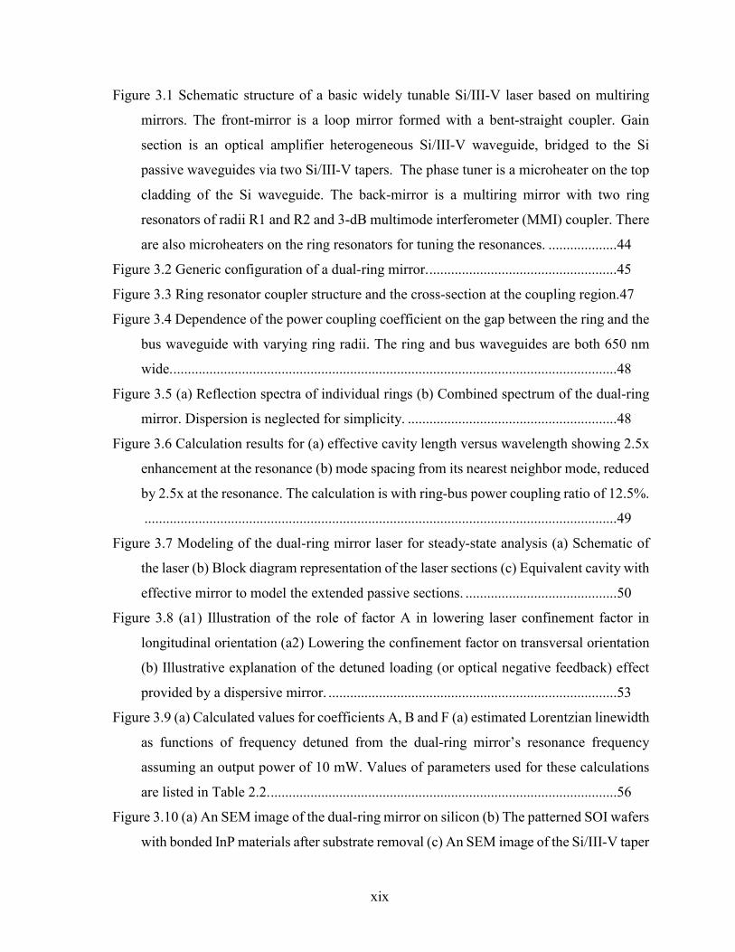
Figure 3.13 Mode hopping behavior in the tunable laser (a) Mode-hops between two adjacent
longitudinal modes by tuning the phase section (b) Mode-hops between two ring’s modes
by tuning one of the ring resonators. ......................................................................... 60
Figure 3.14 (a) Frequency noise spectrum of the fabricated dual-ring mirror laser measured at
120 mA. The inset replots the figure with frequency in linear scale to clearly show the
white noise level (b) Best linewidth measured at wavelengths across the tuning range.
................................................................................................................................... 62
Figure 3.15 (a) Frequency noise spectra of the dual-ring mirror laser when the lasing frequency
is detuned away from resonance peak (b) Laser output power and the extracted linewidth
from frequency noise measurement as functions of the detuned frequency. The dash-line
show the theoretical curve calculated in Figure 3.9(b). ............................................. 63
Figure 4.1 Simulated Lorentzian linewidth of widely-tunable laser as a function of coupling
strength of the high-Q ring for four waveguide propagation loss scenarios. Calculation
follows the analysis and parameters in [1]. © MDPI 2018 ....................................... 67
Figure 4.2 (a) Cross-sectional geometry of the ultra-low loss (ULL) Si waveguides. The 56
nm tall Si rib is formed by dry-etching, leaving a 444 nm thick Si slab. (b) Effective index
versus waveguide width in the 56 nm rib Si waveguide. The waveguide is quasi-single
mode within the yellow colored region. Inset: Electric field profile of the fundamental
mode in 1.8 µm wide waveguide. © MDPI 2018 ...................................................... 68
Figure 4.3 (a) Experimental data (circular markers) and theoretical curve (solid line) for the
propagation loss of 1 µm wide waveguide at varying etch depth. (b) Theoretical
calculations (solid lines) of the waveguide loss at varying waveguide width at three

xxi
different etch depth (500 nm, 231 nm and 56 nm). The measured results are plotted in
circular markers. © MDPI 2018 ................................................................................ 70
Figure 4.4 (a) Mask layout of spiral delay lines with 52.2 cm total length and 850 m
minimum bend radius (b) Optical Backscatter Reflectometry (OBR) data from the spiral
with 1.8 µm width. A linear fit of the waveguide backscatter is shown with the dashed
red line. The propagation loss of the waveguide can be approximated as 1/2 of the slope
of the fitted line. (c) Wavelength dependence of the propagation loss (mean and standard
deviation) of waveguides with different widths (1.8 µm, 3.0 µm and 8.0 µm). © MDPI
2018 ........................................................................................................................... 71
Figure 4.5. (a) Measured spectral responses of the 750 µm radius Si ring resonator (all-pass
configuration) plotted with a Lorentzian fit. The extracted intrinsic quality factor Qint =
4.1 million. (b) Simulated bend-loss limited intrinsic Q of the rings versus ring radius at
three etch depths. The experimental data of the targeted 56 nm etch depth are depicted as
blue circular markers. © MDPI 2018 ........................................................................ 74
Figure 4.6 (a) An SEM image of the fabricated low Bragg grating waveguide with a close-
up of the holes on both sides of the waveguide. (b) Theoretical calculations of gratings’
full width half max (FWHM) versus varying L for 0.5, 1 and 2 cm long grating
waveguides. Circular blue markers show the measured data. (c-d) Spectra of reflection
and transmission of 1 cm long grating waveguides with κ=1.25 cm-1 and κ=4.0 cm-1,
respectively. The ripples are caused by reflections off the waveguide facets. (e) The
extracted n, and exponential fit as a function of waveguide to hole distance. © MDPI
2018 ........................................................................................................................... 76
Figure 4.7 Schematic of the taper converting the optical mode from an ULL waveguide to
standard rib (231 nm etch-depth) waveguide. Figures (a), (b) and (c) show the waveguide
mode profiles at locations labeled a – ULL silicon waveguide, b – central part of the
taper, and c - standard silicon waveguide along the taper structure. © MDPI 2018 . 77
Figure 4.8 (a) Simulation results at 1550 nm wavelength of the optical transmissions and
reflections at the deep-shallow taper. The fundamental mode was launched from the ULL
silicon waveguide side. Transmitted and reflected powers to the fundamental mode and
high order modes were simulated using two methods. The solid lines show the results

xxii
using mode expansion simulation, while the markers are the data points simulated with
FDTD (b) Wavelength dependence of the transmission and reflection from fundamental
input mode to fundamental output mode, simulated with FDTD. © MDPI 2018 ..... 78
Figure 5.1 Conceptual illustration of the ultralow noise tunable laser integrated on Si/III-V.
................................................................................................................................... 82
Figure 5.2 Schematic of tunable lasers. The front-mirror is a tunable-mirror formed with an
MZI tunable directional coupler. Gain section is an optical amplifier heterogeneous
Si/III-V waveguide, connected to the Si passive waveguides via two Si/III-V tapers. The
phase tuner is a microheater on the top cladding of the Si waveguide. The back-mirror is
a multiring mirror with, (a) three rings, (b) four rings, and a tunable coupler. 231 nm etch
Si waveguides are drawn in black while 56 nm etch Si waveguides are in blue. ...... 83
Figure 5.3 (a) Schematic of the ring-bus coupler structure for simulation. (b) Power cross
coupling ratio as a function of the ring radius and the gap between the ring and bus
waveguide. ................................................................................................................. 85
Figure 5.4 Reflection spectrum of dual-ring mirror structure with large bend radii (~600 µm)
shows low side mode suppression ratio. Plot (b) is the close-up of (a). .................... 86
Figure 5.5 Generic configuration of (a) triple-ring mirror (b) quad-ring mirror. .............. 86
Figure 5.6 Reflection spectra of the triple-ring mirror (a) Broad spectrum shows the
wavelength response across two Vernier FSRs (b) Close-in spectrum shows the
sidemodes near the central reflection resonance peak with SMSR >8 dB. ............... 88
Figure 5.7 Reflection spectra of the quad-ring mirror (a) Broad spectrum shows the
wavelength response across two Vernier FSRs (b) Close-in spectrum shows the
sidemodes near the central reflection resonance peak with SMSR >16 dB. ............. 89
Figure 5.8 Effective cavity length of the laser with (a) the triple-ring mirror (b) the quad-ring
mirror. ........................................................................................................................ 89
Figure 5.9 Calculated values for coefficients A, B and F and estimated Lorentzian linewidth
as functions of frequency detuned from the reflection peak resonance for a laser output
power of 10 mW. Values of parameters used for these calculations are listed in Table
5.1 and Table 5.2. Figures (a-b) are of the triple-ring mirror laser and (c-d) are of the
quad-ring mirror laser. ............................................................................................... 91

xxiii
Figure 5.10 (a) Microscopic images of a fabricated triple-ring mirror laser (b) Microscopic
images of a fabricated triple-ring mirror laser. (i) SEM image of a Si/III-V taper. (ii)
SEM image of a transition from 56 nm to 231 nm etched waveguides. .................... 92
Figure 5.11 (a) Current-voltage relation of the 2.5 mm long gain section (b) The light-current
curve of the triple-ring laser. The lasing wavelength was not kept constant across the
current sweeping, shown in the right y-axis. ............................................................. 94
Figure 5.12 Tuning characteristic of the triple-ring mirror laser: (a) Course tuning spectra
showing the tuning range of 110 nm (b) Two-dimensional wavelength tuning map of the
dual-ring mirror laser. The color indicates the lasing wavelength in unit of nm. (c) Side-
mode suppression ratio (SMSR) of the corresponding wavelength tuning map, showing
>40 dB on most of the operation points. .................................................................... 95
Figure 5.13 Tuning characteristic of the fabricated quad-ring mirror laser: (a) Course tuning
spectra showing the tuning range of 120 nm (b) Two-dimensional wavelength tuning
map of the dual-ring mirror laser. (c) Side-mode suppression ratio (SMSR) of the
corresponding wavelength tuning map. ..................................................................... 96
Figure 5.14 (a) Frequency noise spectrum of the fabricated triple-ring mirror laser measured
at 300 mA. (b) The same spectrum plotted with x-axis in linear scale to zoom-in on the
noise at high frequency range. An upper bound of 70 Hz2/Hz for the white noise level is
drawn. ........................................................................................................................ 97
Figure 5.15. (a) Frequency noise spectrum of the fabricated quad-ring mirror laser. (b) The
same spectrum plotted with x-axis in linear scale to zoom-in on the noise at high
frequency range. The spikes at 18 MHz and harmonics are from the measurement tool.
A white noise level of 45 Hz2/Hz is drawn. ............................................................... 99
Figure 6.1 Concept of the ultralow noise extended-DBR laser on Si/III-V integrated platform.
................................................................................................................................. 101
Figure 6.2 Impact of grating strength on the (a) full-width half maximum (FWHM) bandwidth
and (b) reflected power assuming a 15mm long uniform grating. The simulations are
shown over various lengths and waveguide losses. ................................................. 102
Figure 6.3 (a) Schematic of the E-DBR laser. A ring resonator is incorporated in the cavity
(b) to form the RAE-DBR laser. .............................................................................. 103

xxiv
Figure 6.4 (a) Test setup used to characterize the grating-based reflectors in each laser without
having to use separate test structures. The measurements for the E-DBR are shown in (b)
for a 15mm long grating with designed L = 0.375, 0.75, and 3 respectively. The
measurement for the RAE-DBR is shown in (c), in which the transmission through both
the grating and ring is recorded. By tuning the ring across a full FSR, the shape of the
grating can be revealed. ........................................................................................... 105
Figure 6.5 (a) LIV curve for the E-DBR laser with L = 0.375 with and without active tuning
of the phase control section. The on-chip output power reaches over 37mW. The LI
characteristics of the RAE-DBR are shown in (b), with and without active tuning of the
ring heater. ............................................................................................................... 108
Figure 6.6 At a fixed gain of 200mA, the laser encounters different multi-mode regimes, which
are shaded, depending on whether the longitudinal modes are (a) red-shifted with
increasing power to the phase section, or (b) blue-shifted. In the multimode regions (c),
the laser can enter a mode-locked state (2) or a chaotic state (3). ........................... 109
Figure 6.7 Frequency noise spectra for the E-DBR and RAE-DBR lasers on (a) logarithmic
and (b) linear frequency scales. The analyzer is limited to 20MHz, which may not be
sufficient to see the white noise floor of the FN. ..................................................... 111
Figure 6.8 Measured Relative Intensity Noise (RIN) of the E-DBR with κL = 0.375 at different
drive currents. .......................................................................................................... 112
Figure 7.1 Minimum configuration of a reciprocal optical Sagnac interferometer, consisting
of an optical source, optical power splitter, photodetector, phase modulator, polarizer
(optional) and a sensing coil. ©OSA 2016 .............................................................. 115
Figure 7.2 Three-dimensional schematic (not to scale) of the integrated optical driver (IOD)
for fiber optic gyroscopes. ©OSA 2017 .................................................................. 117
Figure 7.3 Picture of a fabricated IOD chip with close-up images of its components. LS: Light
Source, PD: Photodiode, PM: Phase Modulator. A set of 12 devices is placed next to a
US quarter coin for size comparison. ©OSA 2017 ................................................. 118
Figure 7.4 (a) Schematic of the interferometric optical gyroscope driven by the IOD chip. The
PM fiber coil is 180 m long with a diameter of 20 cm. LS: Light Source, PD: Photodiode,
PM: Phase Modulator, PMF: Polarization Maintaining Fiber, ESA: Electrical Spectrum

xxv
Analyzer, FG: Function Generator. (b) Photograph of the electrical and optical alignment
onto the IOD chip. ©OSA 2017 .............................................................................. 118
Figure 7.5 (a) IOD driven gyroscope’s signal versus the rotation rate. Inset shows a zoom-in
of small range of the rotation rate. (b) The spectra on the ESA of CW and CCW 2 °/s and
zero-rotation. The plot is centered at the 560 kHz modulation frequency with the
resolution width of 1 Hz. ©OSA 2017 .................................................................... 120
Figure 7.6 Measured spectra and corresponding coherence function for DFB laser. The three
rows correspond to: (a) continuous wave (coherence length Lc = 1871 mm,
underestimated due to measurement method) (b) single-tone modulation (300 MHz, Lc
= 42 mm) (c) two-tone modulation (300 MHz and 99 MHz, Lc = 48 mm). By applying
fast FM modulation, the coherence length can be reduced by approximately two orders
of magnitude. ©OSA 2016 ...................................................................................... 123
Figure 7.7 Measured spectra and corresponding coherence function for FP laser. The two rows
correspond to: (a) continuous wave (coherence length Lc = 145 mm) (b) single-tone
modulation (300 MHz, Lc = 47 mm). ©OSA 2016 ................................................. 125
Figure 7.8 Schematic of in-house assembled fiber-based optical gyroscope. All fibers after the
first polarizer are PM and input polarization are optimized for maximum power at the
photodiode. Each fiber component is connected to the next by an FC/APC. ©OSA 2016
................................................................................................................................. 127
Figure 7.9 Allan deviation measurements for each optical source at CW, single, and two-tone
modulation. FM modulation improves both the ARW and bias stability in all cases.
©OSA 2016 ............................................................................................................. 128
Figure 8.1. Widely-tunable integrated lasers linewidth progress in time. The arrows show the
progress of results accomplished in the scope of this dissertation. ......................... 134
Figure A1.1 Schematic configurations of multiring mirrors (a) Single-ring (1R) mirror (b)
Dual-ring (2R) mirror (c) Triple-ring (3R) mirror (d) Quad-ring (4R) mirrors. The heaters
above the waveguides are used to change the local temperature of the rings, allowing
resonance tuning due to thermo-optic effect. ........................................................... 139
Figure A1.2 (a) Schematic of an add-drop ring resonator filter with two bus waveguides
coupled to a ring resonator (b) Signal-flow graph of the same add-drop ring resonator
filter. ......................................................................................................................... 141

xxvi
Figure A1.3 (a) Add-drop filter with output at the through port (b) Signal-flow graph shows
the two forward paths from the input to the output at the through port. .................. 142
Figure A1.4 (a) Single-ring mirror schematic. The mirror is comprised of a 2x2 (or 1x2)
couplers and two bus waveguides coupling to a ring resonator to form a loop. (b) The
equivalent signal flow graph. ................................................................................... 144
Figure A1.5 Single-ring mirror schematic with the annotation for the analysis ............. 146
Figure A1.6 Reflection spectra of single-ring mirror structures with different sets of
parameters ................................................................................................................ 147
Figure A1.7 Dual-ring mirror schematic. The mirror is comprised of a 2x2 (or 1x2) couplers
and two cascaded add-drop filters. .......................................................................... 149
Figure A1.8 Reflection spectra of dual-ring mirror structures with various values of bend radii
and coupling ratios. Plot (b), (d) and (f) are the close-up of (a), (c) and (e), respectively.
These bend radii and waveguide loss are representative for the standard Silicon 231 nm
etched waveguides. .................................................................................................. 150
Figure A1.9 Reflection spectra of dual-ring mirror structures with large bend radii (~600 µm)
shows low side mode suppression ratio. Plot (b) and (d) are the close-up of (a) and (c)
respectively. ............................................................................................................. 151
Figure A1.10 Triple-ring (3R) and Quad-ring (4R) mirror schematics. .......................... 152
Figure A1.11 Reflection spectra of triple-ring mirror structure (a, b) with ~60 µm bend radii
shows significantly improved SMSR compared to that of the dual-ring mirror shown in
Figure A1.8 (c) and (d). ........................................................................................... 152
Figure A1.12 Reflection spectra of triple-ring mirror structure (a, b) with large bend radii
(~600 µm) shows significantly improved SMSR compared to that of the dual-ring mirror
shown in Figure A1.9. Quad-ring mirror structure (c, d) further improves the
performance. Plots (b) and (d) are the close-up of (a) and (c), respectively. .......... 153
Figure A2.1 (a) Schematic of an UMZI. b) Optical spectra of transmissions through a UMZI
structure. The spectra were simulated with the coupling ratios of the two couplers being
0.3 and 0.4, path length difference L = 500 µm and a propagation loss 10 dB/cm.
Extinction ratios are denoted by R13, R14, R23 and R24. ©IEEE 2016 ..................... 156
Figure A2.2 a) The measurement setup using a tunable laser source (TLS), a single mode fiber
polarization controller (PC) and a power sensor. b) An alternative configuration using a

xxvii
broadband source (e.g. ASE) with an optical spectrum analyzer (OSA). ©IEEE 2016
................................................................................................................................. 160
Figure A2.3 (a) Schematic of the Si3N4 waveguide UMZI with 62.1 cm length difference (b)
An SEM image of a set of silicon waveguide UMZI structures for coupling ratio
characterization. ©IEEE 2016 ................................................................................. 161
Figure A2.4 Optical spectra of the transmissions through the UMZI fabricated on Si3N4
waveguide platform. The path length difference is 62.1 cm. The peaks and valleys do not
line-up due to the limited ±1 pm of swept wavelength repeatability. ©IEEE 2016 162
Figure A2.5 Optical spectra of the transmissions through the UMZI fabricated on Si3N4
waveguide platform. ©IEEE 2016 ........................................................................... 163
Figure A2.6 The coupling ratio versus coupler length of the Si directional couplers at two
wavelengths 1525 nm and 1575 nm. The measured data are plotted together with
theoretical fitting curves. ©IEEE 2016 .................................................................... 163
Figure A3.1 Modified fabrication procedure for the Si/III-V lasers. The process begins with
silicon processing (1-6) with patterning of waveguides and gratings. The III-V epi is
bonded (7), followed by patterning of the mesa (8-10), etching of the p-InP, MQW, and
n-InP layers. The mesas are passivated, followed by metallization of the n-contact (11),
p-contacts (12), heaters (13) and probe metal (14). ................................................. 168

xxviii
LIST OF TABLES
Table 2.1 Epitaxial III- V Layer Structure Used for the Lasers and Photodiodes ............. 30
Table 2.2 Epitaxial III-V Layer Structure Used for the Phase Modulators ....................... 37
Table 3.1 List of parameters used for the laser design ...................................................... 55
Table 5.1 Multi-ring mirror design parameters ................................................................. 87
Table 5.2 List of parameters used for laser linewidth calculations ................................... 90
Table 6.1 Comparison of Lorentzian linewidth of E-DBR and RAE-DBR lasers .......... 111
Table 7.1 Key performance indicators for ASE and laser-based gyroscope measurements. FM
modulation improves both the ARW and bias instability. ©OSA 2016 .................. 128
Table 8.1 Comparison of foundry -compatible low loss single mode waveguide platforms
................................................................................................................................. 133
Table A2.1 Extinction ratios and values of parameters l, m, n, p .................................... 162

1
Chapter 1. Introduction
1.1 Ultralow noise semiconductor lasers
Ultralow noise (ULN) semiconductor lasers are required for a wide range of applications,
including high performance coherent communications systems [1], ultra-precise timing [2],
frequency synthesis [3], spectroscopy [4], and distributed sensing systems [5]. Furthermore,
there is significant demand for ULN lasers in RF photonic analog links and processing [6]–
[8], as well as optically processed phase array antennas. ULN is a key requirement to any
system involving optical mixing, as the noise of the laser will directly affect the fidelity of the
generated RF signals. For example, two ULN lasers can be beat together in a high-speed
photodetector to generate a stable microwave signal [9], [10]. Another major use of ULN
lasers requiring extremely low phase noise is in the fiber optic sensing field, such as
interferometric acoustic sensing systems for exploration or sonar sensing systems or
distributed sensing systems. Finally, yet another fast-growing sensing application is LiDAR,
where the low frequency phase noise again directly impacts system performance. The
common requirements for all these applications are very low relative intensity noise (RIN) as
well as very low frequency noise and Lorentzian linewidth. Current commercial solid state
lasers [11], [12] and fiber lasers [13], [14] have high performance, but cannot compete with
semiconductor lasers in terms of size, weight, and power (SWaP), or cost.
Recently, there has been significant interest in assembling semiconductor gain chips with long
external cavities to reduce the laser linewidth. This hybrid approach is attractive because it
allows for the gain chip and external cavity to be separately optimized. This starts with the
material selection, and external cavities based on planar lightwave circuits (PLC) [15], low-
loss silicon nitride [16], [17], and silicon [18], [19] have been demonstrated. The drawback

2
regarding these assembled hybrid semiconductor lasers is their limited scalability, as each
laser must be individually assembled. Alignment between the chips is critical, which slows
down the process and increases cost. Furthermore, many of the aforementioned sensing
applications require that the devices are resistant to variations in pressure, shock, and
vibration. This is another reason why a fully integrated solution is preferred over hybrid
solutions, as the coupling between the gain chip and external cavity is sensitive to these
environmental factors.
The heterogeneous silicon/III-V integration platform provides an excellent solution to this
problem [20], [21]. Heterogeneous integration involves the wafer bonding of unprocessed
materials on a wafer level scale, providing a clear path towards scaling and high-volume
production. It benefits from mature CMOS-based silicon processing technologies and
foundries. Heterogeneous integration also has the benefit of selecting the best material to
perform each function (i.e. lasers, low-loss waveguides, detectors) to form highly complex
photonic integrated circuits (PIC) [22]. Thus, it provides much more flexibility compared to
a purely monolithic approach, while retaining the much-needed scalability that hybrid
solutions lack.
Figure 1.1, replotted from [23], reflects the trend in semiconductor laser noise in the past
decades. Although being only focused on widely tunable lasers, it does provide readers with
the research process on semiconductor laser noise in general. Here, the authors compared the
spectral linewidth of widely-tunable lasers on the three main categories: III/V based
monolithic lasers, hybrid lasers where III/V gain chips are butt coupled to passive chips, and
heterogeneous integrated lasers where the III/V gain material is bonded to silicon. It can be
clearly observed that the III-V conventional monolithic lasers, mostly SGDBR types, have the

3
linewidth reduced with time but the best results are still around ~70s of kHz. The hybrid lasers
with multiple chips assembled show far more superior linewidth performances, down to ~300
Hz level, thanks to the low loss external cavity on a separated chip. The heterogeneous Si/III-
V lasers have made good progress in the past 5 years, and the lowest reported linewidth was
~50 kHz, prior to this thesis.
Figure 1.1 Widely-tunable integrated lasers linewidth progress in time. The authors make a
distinction between III/V based monolithic lasers, hybrid lasers where III/V gain chips are
butt coupled to passive chips, and heterogeneous integrated lasers where the III/V gain
material is bonded to silicon. Reproduced from [23]. © MDPI 2017
1.2 Thesis objectives
The goal of this work is to lower the linewidth in heterogeneous Si/III-V lasers to 100s Hz
linewidth level. To accomplish this immense improvement, we first revisit and optimize the
architectural design of the heterogeneous Si/III-V integration platform based upon the work
developed at UCSB over years [24]–[26]. This step would be crucial in high performances of

4
photonic components on device level, as well as photonic integrated circuits on system level.
We then implement new waveguide structures to achieve ultralow propagation loss on silicon
waveguides. High performing silicon passive components are then be seamlessly adopted as
an integral part of the Si/III-V laser cavity to deliver ultralow noise lasers fully integrated on
silicon.
1.3 Thesis outline
This thesis presents the development of an advanced class of fully integrated laser diodes with
ultralow frequency noise for use in photonic integrated circuits. The optimization includes
redesigning or newly designing numerous photonic components.
Chapter 2 focuses on optimizing heterogeneous Si/III-V photonic architecture for high
performing photonic circuits in general. It begins with selection of the waveguide architecture
for maximum freedom in active component design space. Basic passive and active
components’ designs and characteristics will be described. This is the photonic platform upon
which all the lasers and photonic circuits in this thesis are built.
Next, in Chapter 3, we describe the details of the designs, theoretical modeling, and complete
characterization of dual-ring mirror based tunable lasers using the standard waveguides on the
heterogeneous Si/III-V photonic platform developed in Chapter 2.
Chapter 4 contains details of the development of ultralow loss silicon waveguides. Design
considerations, theoretical analysis and characterization results of the ultralow loss waveguide
and its derived high Q resonant photonic passive devices is presented.
Chapter 5 shows the designs and characteristics of the first class of ultralow noise lasers based
on multiring mirror as the extended cavity. The laser diodes simultaneously accomplish an
ultrawide wavelength tuning range and an ultralow frequency noise.

5
Chapter 6 presents the second class of the ultralow noise lasers based on a physically long and
weak Bragg gratings. The characteristics of mode hopping, as well as frequency and RIN
noise will be discussed.
Chapter 7 showcases a successful photonic integrated circuit which is comprised of all device
components on the heterogeneous Si/III-V photonic platform. The design, characterization of
gyroscope sensitivity and potential of frequency modulated lasers in lowering gyroscope’s
noise will be discussed.
Chapter 8 concludes with a summary of achievements and comparison with other material
system regarding waveguide loss and laser linewidth. It will end with a proposal for future
work for further improvements of the laser performances
There are three appendices at the end of the thesis. Appendix 1 presents a rigorous and
thorough analysis of the spectral responses of generic multiring mirrors, which were the key
structures for the widely tunable low noise lasers. Appendix 2 describes a robust method for
characterizing waveguides and couplers using UMZI test structures. Finally, Appendix 3
shows a brief fabrication process flow of the devices in this work.

6
References
[1] S. L. I. Olsson, J. Cho, S. Chandrasekhar, X. Chen, P. J. Winzer, and S. Makovejs,
“Probabilistically shaped PDM 4096-QAM transmission over up to 200 km of fiber
using standard intradyne detection,” Opt. Express, vol. 26, no. 4, p. 4522, 2018.
[2] Z. L. Newman et al., “Photonic integration of an optical atomic clock,” arXiv, 2018.
[3] D. T. Spencer et al., “An optical-frequency synthesizer using integrated photonics,”
Nature, vol. 557, pp. 81–85, 2018.
[4] M. G. Suh, Q. F. Yang, K. Y. Yang, X. Yi, and K. J. Vahala, “Microresonator soliton
dual-comb spectroscopy,” Science (80-. )., vol. 354, no. 6312, pp. 1–9, 2016.
[5] J. Geng, C. Spiegelberg, S. Jiang, and A. Abstract, “Narrow Linewidth Fiber Laser for
100-km Optical Frequency Domain Reflectometry,” IEEE Photonics Technol. Lett.,
vol. 17, no. 9, pp. 1827–1829, 2005.
[6] C. Middleton, S. Meredith, R. Peach, and R. Desalvo, “Photonic frequency conversion
for wideband RF-to-IF down-conversion and digitization,” 2011 IEEE Avion. Fiber-
Opt. Photonics Technol. Conf., pp. 115–116, 2011.
[7] D. Marpaung, C. Roeloffzen, Heideman, Rene G., Leinse, Arne, S. Sales, and J.
Campany, “Integrated microwave photonics,” Laser Photon. Rev., vol. 7, no. 4, pp.
506–538, 2013.
[8] P. A. Morton and Z. Mizrahi, “Low-cost, low-noise hybrid lasers for high SFDR RF
photonic links,” 2012 IEEE Avion. Fiber- Opt. Photonics Technol. Conf., pp. 64–65,
2012.
[9] J. Hulme et al., “Fully integrated microwave frequency synthesizer on heterogeneous
silicon-III/V,” Opt. Express, vol. 25, no. 3, p. 2422, 2017.

7
[10] J. Yao, “Microwave Photonics : Photonic Generation of Microwave and Millimeter-
wave Microwave Photonics : Photonic Generation of Microwave and Millimeter-wave
Signals,” Int. J. Microw. Opt. Technol., vol. 5, no. 1, pp. 16–21, 2010.
[11] T. J. Kane and R. L. Byer, “Monolithic, unidirectional single-mode Nd:YAG ring
laser,” Opt. Lett., vol. 10, no. 2, p. 65, 1985.
[12] “Continuous Wave Single Frequency IR Laser NPRO 125/126 Series.” .
[13] “NP Photonics.” .
[14] “Koheras AdjustiK E15.” .
[15] A. Verdier, G. De Valicourt, R. Brenot, H. Debregeas, H. Carr, and Y. Chen,
“Ultrawideband Wavelength-Tunable Hybrid External-Cavity Lasers,” J. Light.
Technol., vol. 36, no. 1, pp. 37–43, 2018.
[16] B. Stern, X. Ji, A. Dutt, and M. Lipson, “Compact narrow-linewidth integrated laser
based on a low-loss silicon nitride ring resonator,” Opt. Lett., vol. 42, no. 21, p. 4541,
2017.
[17] Y. Fan et al., “290 Hz Intrinsic Linewidth from an Integrated Optical Chip-based
Widely Tunable InP-Si3N4 Hybrid Laser,” Conf. Lasers Electro-Optics, vol. 161, no.
2011, p. 2013, 2017.
[18] H. Guan et al., “Widely-tunable, narrow-linewidth III-V/silicon hybrid external-cavity
laser for coherent communication,” Opt. Express, vol. 26, no. 7, p. 7920, 2018.
[19] N. Kobayashi et al., “Silicon photonic hybrid ring-filter external cavity wavelength
tunable lasers,” J. Light. Technol., vol. 33, no. 6, pp. 1241–1246, 2015.
[20] A. W. Fang, H. Park, O. Cohen, R. Jones, M. J. Paniccia, and J. E. Bowers, “Electrically
pumped hybrid AlGaInAs-silicon evanescent laser,” Opt. Express, vol. 14, no. 20, p.

8
9203, 2006.
[21] T. Komljenovic et al., “Heterogeneous Silicon Photonic Integrated Circuits,” J. Light.
Technol., vol. 34, no. 1, pp. 1–1, 2015.
[22] T. Komljenovic, D. Huang, P. Pintus, M. A. Tran, M. L. Davenport, and J. E. Bowers,
“Photonic Integrated Circuits Using Heterogeneous Integration on Silicon,”
Proceedings of the IEEE. 2018.
[23] T. Komljenovic et al., “Widely-Tunable Ring-Resonator Semiconductor Lasers,” Appl.
Sci., vol. 7, no. 7, p. 732, 2017.
[24] A. W. Fang, “Silicon evanescent lasers,” ProQuest Diss. Theses, no. March, p. 155,
2008.
[25] M. L. Davenport, “Heterogeneous Silicon III-V Mode-Locked Lasers,” UCSB, 2017.
[26] T. Komljenovic, D. Huang, P. Pintus, M. A. Tran, M. L. Davenport, and J. E. Bowers,
“Photonic Integrated Circuits Using Heterogeneous Integration on Silicon,” Proc.
IEEE, pp. 1–12, 2018.

9
Chapter 2. Heterogeneous Silicon/III-V Photonic Platform
This chapter present the designs and characteristics of key building block components in the
heterogeneous Si/III-V photonic platform. We begin with selection of the optimal waveguide
architecture, including the silicon device thickness and waveguide geometry. Then, we discuss
several essential building blocks for integrated circuits, from passive to active components.
The component designs and characteristics are explained.
2.1 Silicon photonic waveguides
2.1.1 Thickness selection
To enable a full design space for photonic devices in Si/III-V heterogeneous platform,
maximum control of the optical mode confinement in the gain (III-V) layer and passive
(silicon) layer should be obtained by engineering the waveguide widths of the III-V and silicon
waveguides. In principle, as described in [1], [2], the ratio between effective indices of the
individual III-V guide and that of the silicon guide should be tailorable from above unity
(regime a.1 in Figure 2.1a) to below unity (regime a.3 in Figure 2.1a). When this condition
is satisfied, an efficient and low loss optical mode transfer between the active region (III-V
guides) and passive region (Si guides) can be made. For that requirement, the thickness of the
SOI waveguides needs to be optimized in accordance to the III-V stacks. For vertical injection
devices - the typical choice for most lasers and amplifiers, the III-V stack total thickness is
roughly about 2 µm to separate the contact metal sufficiently far from the optical mode to
avoid carrier absorption loss in the optical mode. As shown in Figure 2.1b, a thickness of 500
nm for the silicon layer results in a good index match with the III-V layer, allowing for a great
flexibility in designing the mode hybridization. Other considered thicknesses, such as the

10
widely utilized 220 nm SOI waveguides [3] or multi-micron thick SOI waveguides [4], do not
suit well because their indices are fairly far off from that of the III-V. The thickness of the
silicon layer in devices developed through out all the work done in this dissertation, therefore,
was chosen to be 500 nm.
Figure 2.1 (a) Optical mode profiles of the heterogeneous (Si/III-V) waveguide with 500 nm
thick silicon in 3 different operating regimes: (a.1) with a slab III-V on 0.7 µm wide silicon
waveguide, which results in higher confinement in the active III-V layer. (a.2) with a slab
III-V on 1.3 µm wide silicon waveguide, which results in equal confinement in the III-V and
silicon. (a.3) with 0.5 µm wide III-V on 1.3 µm wide silicon waveguide, which results in
higher confinement in silicon. (b) Effective indices of strip silicon waveguides of three
thicknesses (220 nm, 500 nm and 3 µm) with varying width is plotted together with the
effective index of a typical 2 µm thick III-V waveguide (used in [5]). Noted that all simulations
were carried out at 1550 nm wavelength. © MDPI 2018
This section describes the details of the passive optical devices developed on the 500 nm thick
SOI platform. We first start with the fundamental designs of the silicon rib waveguides and

11
discussion of the waveguide bends and waveguide terminations that are necessary elements
in photonic circuits.
2.1.2 Waveguide designs
The waveguide geometry should be designed to meet the requirement of single mode
operation. As integrated waveguides are typically confined vertically and laterally, the
thickness of the core layer and the width of the waveguide play major roles in number of
modes that are guided. Due to the characteristics of lithographic fabrication, one has great
flexibility in varying the waveguide width (normally defined by etching) for lateral
confinement while very little in the waveguide thickness (determined by material growth,
bonding or deposition) for vertical confinement. We first inspect the vertical confinement by
looking at modes guided in a slab waveguide structure shown in Figure 2.2a, where silicon
is the core and silicon dioxide is used for bottom and top cladding. Figure 2.2b shows the
effective indices of the guided modes with increasing silicon thickness. The cut-off thickness
for single mode regime is roughly about 250 nm for TE polarization. With silicon thickness
in this single-mode regime, one guarantees the single-mode operation in the vertical direction,
and therefore can easily achieve single-mode waveguide with strip geometry as long as the
width of the waveguide is chosen to not be too wide to support only single mode laterally.
This is also the very reason that 220 nm was chosen and became the most commonly used in
silicon photonics.

12
Figure 2.2 (a) Schematic of a slab (1D) waveguide where the mode is confined vertically (b)
Guided slab mode indices calculation at varying silicon thickness. c) Mode profiles of the TE0
mode and d) TE1 mode in a 500 nm thick silicon slab waveguide.
As opposed to the widely used 220 nm thick waveguides, the 500 nm thickness that we use
for the Si/III-V integration is far outside of the single mode regime. Other than the
fundamental TE mode (Figure 2.2c), there also exists a high order TE mode guided vertically
which is the TE1 mode plotted in Figure 2.2d. Strip waveguide geometry (silicon fully etched)
with 500 nm thick silicon, therefore, supports multi-modes. Fortunately, quasi-single mode
operation can be achieved with slightly modified geometry: a rib waveguide. For the rib
waveguides, the silicon core would be only partially etched, forming a “rib” on the silicon
slabs. Since the high order modes in the vertical direction of the waveguide have multi-peaked
intensity distribution (“lobes”) along the vertical axis, one of the lobes could couple into the

13
fundamental mode of the slab. The coupling to the slab modes works as a lateral leak-out
mechanism to filter out high order modes in rib waveguides. The first essential design rule for
filtering out the first vertical high-order mode is that the slab height must be larger than half
of the waveguide’s total height. With that being satisfied, the index of the slab’s fundamental
mode becomes larger than that of the first-order mode of the rib and effectively forces the
high order modes to leak out.
A more rigorous and thorough analysis of the use of rib waveguide to achieve quasi-single
mode operation for generic large rib waveguides is first provided by R. Soref et al. [6] and
later refined and strengthened by S. Pogossian et al. [7]. The most important results from their
work are the following Equations (2.1) and (2.2) which show the single-mode condition for a
general rib-waveguide geometry. The geometry parameters h, W and H are respectively slab
height, waveguide width and the total height of the waveguides as illustrated in Figure 2.3b.
The constant c in the equation (2.1) (2.1) is determined by the material indices. In the case
of a silicon waveguide with air as the top-cladding and silicon dioxide as the bottom cladding,
c=0 should be used [8].
0.5h
H (2.1)
2
/
1 ( / )
W h Hc
H h H
(2.2)

14
Figure 2.3 Schematic cross section of (a) Strip waveguide (fully etched) and (b) Rib waveguide
(partially etched). W: waveguide width, H: Total waveguide height (or thickness), h: slab
height (thickness).
As the total height of our Si waveguide is pre-determined to be 500 nm, the next parameter to
determine in our waveguide design is the height of the rib. According to the analysis above,
the single mode condition can be achieved as long as the slab height is larger than 250 nm,
i.e. the etch depth for the rib formation is less than 250 nm. For the best control of the etch
depth in the fabrication of the waveguides, we use an in-situ etch depth monitor system
(Intellemetrics LEP500 Etch Depth Monitor [9]) available in the UCSB Nanofab cleanroom.
It is a laser reflectometry system in which a laser beam (of 670 nm wavelength) is irradiated
to the samples and the reflected signal is detected by a photodetector. For the stack of 500 nm
silicon on 1000 nm buried oxide, the reflected signal versus the silicon etch is modelled as
shown in Figure 2.4. There are a few favorable etch depths marked in red corresponding to
the notches of the trace. We chose 231 nm etch depth since it is the favorable point closest to
half of the total thickness.

15
Figure 2.4 Reflected power vs etch depth trace of the stack of 500 nm Si on 1000 nm SiO2
using Intellemetrics LEP500 etch monitor system. The etch depths at the notches are labeled
in red.
The last design parameter to determine is the width of the waveguide. A commercial
simulation software was used to calculate the guiding modes with high accuracy. As an
example, the 2D power distribution profiles of TE0, TM0 and TE1 guided in 1000 nm wide
waveguide are shown in Figure 2.5(a, b and c), respectively. The waveguide width is swept
from 1000 nm down to 150 nm and the effective indices of the supported modes are plotted
in Figure 2.5(d). The most important information extracted from the plot is the cut-off
waveguide width for single mode operation for TE polarization, which is about 870 nm. In
practice, we prefer to keep the waveguide width below 800 nm to have a safe margin for
fabrication variations in the waveguide width and especially the etch depth.

16
Figure 2.5 The simulated optical mode profiles a silicon rib waveguide with waveguide width
of 1000 nm, etch depth of 231 nm and Si thickness of 500 nm, (a) Fundamental TE (TE0) (b)
Fundamental TM mode (TM0) (c) First order TE mode (TE1). (d) Effective indices of the
guided modes TE0, TM0 and TE1 at varying waveguide width.
From the plot in Figure 2.5(d) we also see that the cut-off index of the guiding modes for the
231 nm rib waveguide is about 2.98. This cut-off index is exactly equal to the index of the TE
fundamental mode of the 269 nm high slab found in the index plot shown in Figure 2.2b (for
the 1D waveguide). Any optical modes that have index smaller than the cut-off index would
get coupled to the slab mode and leak out, as explained earlier in this section. Therefore, this
cut-off index is also called slab cut-off.
2.1.3 Waveguide routing: bends and terminations
Waveguide routing is inevitable in PICs. The waveguides have to be bent in order to route the
light around the chip and to the optical IO ports. The most commonly used types of bends for
PICs include S shaped bend, 90-degree bend and 180-degree bend. Examples of these bends
are shown in Figure 2.6.
Figure 2.6 Common types of routing bends in photonic integrated circuits (a) S-shaped bend
(b) 90-degree bend and (c) 180-degree bend.

17
It is desirable to have small bend radius to save chip real-estate. Thanks to a high contrast
index between the core (Si) and cladding (oxide or air), fully etched silicon waveguides have
extremely small bend radius, lower than 10 µm [10]. In rib waveguides, since the optical
modes can “leak out” more easily by coupling to the slab modes when bent, the critical bent
radius needs to be larger. For our standard rib waveguides with the 231 nm etch depth, the
bend losses of the fundamental TE mode were simulated with a commercial mode solver
software (shown in Figure 2.1). Considering that the typical waveguide propagation losses of
these waveguide width are about a few dB/cm, we would want to have bend loss lower than
0.1 dB/cm – one order of magnitude lower than the dominant scattering loss. Near the single
mode regime borderline, where waveguide width is about 800 nm, the bend radius should be
larger than 40 µm to have negligible bend loss. Note that the bend loss quickly increases as
the waveguide width decreases, so it is important to check bend loss wherever smaller
waveguides are used.
40 50 60 70 80 90 100 110 120 130 140 150
Bend Radius ( m)
10-8
10-7
10-6
10-5
10-4
10-3
10-2
10-1
100
101
102
Etch Depth = 231 nm
0.5 um
0.6 um
0.7 um
0.8 um
0.9 um

18
Figure 2.7 Simulated bend loss of the fundamental TE mode of the 231 nm etched rib
waveguides for varying waveguide widths.
2.1.3.1 Adiabatic bends
Transitions between two curves that have different curvature could cause power losses due to
the mode mismatch between the modes in the two. As an example, the mode profiles of TE0
modes in straight waveguide and 40 µm radius circular bend of an 800 nm wide rib waveguide
are shown in Figure 2.8(a) and (b), respectively. The difference in the curvatures of the
circular bend (1/40 µm-1 curvature in this case) and a straight waveguide (zero curvature)
resulted in the mode shape and positional mismatch. If the transition between the two is made
continuous (zero waveguide offset) then the TE0 mode from the circular bend would lose
1.14% power in the transmission to the TE0 mode (or 0.057 dB loss) of the straight waveguide.
0.1% (-21.5 dB) power of the circular bend TE0 mode actually excites the fundamental TM0
mode in the straight waveguide. One common mitigation method is to implement a waveguide
offset between straight and circular bend. This intentional offset corrects for the mode
positional mismatch. In the example here, an optimal offset of +37.5 nm reduces the transition
TE0 TE0 loss down to 0.37%. However, the mismatch is still not fully eliminated, resulting
in a transition loss every time a joint from straight to curved waveguide is needed.
A more ideal solution for this problem is to use an adiabatic bend to connect the two
waveguides. The curvature of the adiabatic bend gradually changes from the curvature of the
departure waveguide to that of the destination waveguide. When the curvature change is
gradual and smooth, power loss due to mode mismatch is theoretically eliminated. In this work,
we exploit so-called sine bends to form adiabatic bends.

19
Figure 2.8 (a) Electric field distribution of TE0 mode in straight waveguide (b) Electric field
distribution of TE0 mode in the circular bend (c) Waveguide offset versus power transmission
from circular bend to straight waveguide for TE0TE0 and TE0TM0.
Figure 2.9 (a) Graph of a sine bend connecting two straight waveguides with L = 100 µm
offset in X and H=40 µm offset in Y direction. (b) The curvature and corresponding bend
radius along the sine bend.
An S-shaped full sine bend is mathematically described by the Equation (2.3) below.
sin 22
x H xy H
L L
(2.3)

20
Here, L and H are respectively the offset in the X and Y directions. Figure 2.9(a) plots this
sine bend for the case of L = 100 µm and H=40 µm. The curvature and equivalent bend radius
along the bend is plotted in Figure 2.9(b). The curvature change is continuous at every point
on the bend, allowing for an adiabatic mode transfer between bends that have different
curvatures.
Using parts of the sine bend with an arc of circular bend, we can form 90-degree and 180-
degree bends to connect two straight waveguides pointing in different directions, as illustrated
in Figure 2.10(a-b). The first straight waveguide is connected to a part of a sine bend. The
sine bend gradually changes curvature from zero at one end (contact point to the straight
waveguide) to a non-zero curvature on the other end. A circular bend of the same curvature
would follow and complete the angle rotation. Another part of a sine bend is used at the end
to gradually lower the curvature to zero at the bend’s end point to match with the targeted
straight waveguide.
Figure 2.10 (a) Construction of a 90-degree adiabatic bend from sine bend and circular bend
(b) Construction of 180-degree adiabatic bend from sine bend and circular bend (c)
Curvature along the path length of an adiabatic bend constructed with sine and circular bend.

21
2.1.3.2 Waveguide Terminations
Waveguide terminations are necessary so that unused photons in the circuits should escape
the photonic circuits with negligible effects such as reflection or cross coupling. The simple
way we implement the terminations in this work is to make the waveguide very lossy with
small bend radii. Multiple 180-degree adiabatic bends with decreasing waveguide widths and
bend radii are connected to form multi-turn spiral. To be even safer, the end of the waveguide
termination is angled, as illustrated in Figure 2.11.
Although it is tempting to do as many turns to make the termination extremely lossy, one
should not overuse the number of turns when the termination spirals are under the III-V/Si
bonding area. The small fill factor within the spiral areas (can be seen in Figure 2.11) could
severely hurt the III-V/Si bonding success rates there. In fact, with only several turns at bend
radius of tens of microns, the bending loss should be well below -70 dB, which is already
sufficient for most applications.
Figure 2.11 An example of waveguide termination using multi-turn spiral.

22
2.1.4 Waveguide loss
We fabricated the passive silicon waveguides using deep-UV lithography followed by a
fluorine based pseudo-Bosch dry etching process detailed elsewhere [11]. The etch depth was
achieved within 5 nm deviation thanks to the use of an in-situ etch depth monitor system [9].
Thermal oxide serves as the bottom buried oxide (BOX) while the top cladding is deposited
oxide, either by PECVD or sputtering. Each cladding layer is 1 µm thick to minimize substrate
leakage or loss due to the metal heaters, which are commonly put on the top of the waveguide
for phase tuning. To characterize the waveguide propagation loss, we use the coherent optical
frequency domain reflectometry (OFDR) technique with a commercially available system
(Luna Inc. OBR 4400) [12]. Spirals of waveguides with varying waveguide widths (650 nm,
800 nm, 1 µm and 3 µm) are made with a minimum bend radius of 150 µm, as shown in the
inset of Figure 2.12(a). Since the bend radius used in the spirals is much larger than critical
bend radius even for smallest waveguide width of 650 nm, the propagation loss is not limited
by bend loss. The background doping level of the SOI wafers used here is about 133 10 cm-3,
corresponding to a carrier absorption loss of about 0.001 dB/cm, which is basically negligible.
The loss is, therefore, expected to be dominated by scattering loss, originated from the
waveguide line-edge roughness and sidewall roughness.
The measured OBR trace for the 800 nm wide waveguide is plotted in red color in Figure
2.12(a) A linear fit (black line) is used to calculate the loss, which is half of the fitted slope.
The extracted loss versus wavelength is extracted for all of the waveguides and plotted in
Figure 2.12(b). Loss for typical channel single-mode waveguide – 800 nm width – is lower
than 1 dB/cm. Smaller waveguide of 650 nm width, which is typically used in directional
couplers for strong coupling ratio, has an average loss of 1.2 dB/cm across the C and L bands.

23
Multimode waveguides with larger widths have much lower loss – 0.8 dB/cm for 1 µm width
and 0.65 dB/cm for 3 µm width. This width dependency confirms that the propagation loss is
mainly caused by scattering. As waveguide width increases, the guided fundamental mode is
confined better in the rib and interacts less with the edges of the ribs, effectively leading to
lower scattering loss.
Figure 2.12 (a) Optical Backscatter Reflectometry (OBR) data from the spiral with 800 nm
waveguide width. A linear fit of the waveguide backscatter is shown with the black line. The
propagation loss of the waveguide can be approximated as 1/2 of the slope of the fitted line.
Inset: Microscopic image of a 15 cm long spiral of 800 nm wide waveguide. (b) Extracted
wavelength dependence of the propagation loss of 650 nm, 800 nm, 1 µm and 3 µm wide
waveguides.
2.2 Passive photonic components
2.2.1 IO mode size converters
Due to the large mismatch in the mode field size between Si waveguide and optical fiber, it is
necessary to have a mode size converter at the interface. The two main approaches that are
widely used include vertical grating couplers [13] and edge inverse couplers [14]. While
grating couplers in general have a limited optical bandwidth and an inherent back reflection,

24
edge coupling is preferred because it has broader bandwidth and reduces reflection by angling
or anti-reflection coating. The schematic design of the mode size converter transitioning from
500 nm thick Si waveguide to optical fiber is shown in Figure 2.13(a). The converter
comprises two parts: a bi-level taper and an inverse taper. Through the bi-level taper, the
optical mode from 500 nm x 600 nm rib Si waveguide is squished to the mode in thinner 269
nm x 600 nm Si waveguide. The waveguide is then tapered to 269 nm x 150 nm waveguide.
Since the Si core is now too small, the optical mode is no longer well confined in Si but
expands to the oxide cladding, which largely increases the mode field area and matches better
with optical fibers. The waveguide is also angled to 7° respective to the polished facet to
decrease back reflection.
Figure 2.13 (a) Schematic of the bi-level taper and the inverse taper for waveguide-fiber. The
mode evolution along the coupler is shown to illustrate the working principle. (b) Blue line:
FDTD simulated coupling loss from 269 nm x 150 nm Si waveguide to 2.5 µm spot-size lensed
fiber. Red line: Total coupling loss including the bi-level taper. The waveguide was angled to
7° and the lensed fiber approach angle was 8° respective to the chip facet. © OSA 2017

25
The bi-level taper was simulated with the eigenmode expansion method and the averaged
transmission loss over C-band was estimated to be -0.6 dB. In addition, the coupling efficiency
from the Si inversed taper to a 2.5 µm spot-size fiber was done with FDTD simulation and the
average coupling loss over C-band is about - 2.05 dB, as shown in Figure 2.13(b). In total,
the mode converter is expected to have -2.7 dB coupling loss over the C-band. All simulations
only considered TE mode.
Polarization maintaining (PM) lensed fibers with the mode diameter of ~ 2.5 µm were used to
couple the Si waveguide with mode size converters. Transmission power through a Si straight
waveguide with two mode converters at two ends was recorded while laser wavelength was
swept over 1525 - 1575 nm. The same measurement was also taken for transmission from
fiber to fiber as a reference. The coupling efficiency was then extracted, taking into account
the extra 0.2 dB propagation loss of the 0.2 mm Si straight waveguide, as shown in Figure
2.14. The averaged coupling loss is determined to be -3 dB. The 0.3 dB discrepancy between
measurement and simulation can be attributed to the propagation loss along the mode
converter structure.
Figure 2.14 Coupling efficiency between TE mode of the Si waveguide and 2.5 µm mode
diameter lensed polarization maintaining fiber. © OSA 2017

26
2.2.2 Optical adiabatic couplers
The design of an adiabatic 3-dB 2×2 coupler is illustrated in Figure 2.15(a). The coupler
comprises three sections: the first section (300 µm long) where the two ridge waveguides with
different widths (600 nm and 800 nm wide) slowly come close to each other using S-bends,
the coupling section (400 µm long) where the two asymmetric waveguides are linearly tapered
to 700 nm wide waveguides, and the third section (300 µm long) where each 700 nm wide
waveguide is guided to one of the output waveguides by two other S-bends. We used the
eigenmode expansion method to simulate the propagation of modes through the structure.
Figure 2.15(a) also shows, as an example, how the mode propagates and splits through the
coupler when light is input to the 800 nm wide waveguide. The input mode first excites the
fundamental (even) mode of the coupler modes, then this even mode transmits adiabatically
to the even mode of the symmetric 700 nm wide waveguides at the end of the coupling section;
after that, the power then splits equally to the two output waveguides. The simulation result
in Figure 2.15(b) shows 50±3% splitting ratio of the adiabatic coupler over C+L bands.
Figure 2.15 (a) Schematic of the 3-dB adiabatic coupler. The simulated mode evolution along
the coupler is shown to illustrate the working principle. (b) Simulated wavelength dependence
of the coupler. © OSA 2016

27
Cascading two adiabatic 3-dB couplers back to back with a phase tuner on one of the arms
could form a 2×2 MZI broadband switch. It is worth noting that the two adiabatic couplers are
arranged in such a way that both input and output sides are asymmetric (waveguides are 700
nm and 500 nm wide) while the two waveguide arms connecting the two couplers are both
600 nm wide as shown in Figure 2.16. Theoretically, such configuration results in the switch
being “normally off”, i.e. no light goes through the cross-port when no extra phase difference
is introduced to the MZI arms (see the mode propagation simulation at the bottom of Figure
2.16). The phase is thermo-optically tuned with a heater on the top of one MZI arm.
Figure 2.16 Schematic of the MZI switch based on 3-dB adiabatic couplers. The simulated
mode evolution along the coupler is shown to illustrate the working principle. © IEEE 2016
Both adiabatic coupler and optical switch were then fabricated and tested.
The 2×2 adiabatic 3-dB coupler was characterized by using a rigorous method reported in
[15]. The measurement setup is shown in Figure 2.17(a) with a high-precision tunable laser
source, high precision power sensor, a polarization controller, a polarizer and polarization
maintaining (PM) fibers. The lensed fiber holder rotator was adjusted to launch TE mode

28
(polarization extinction ratio TE/TM > 25 dB) prior to testing. The splitting ratios versus
wavelength plot of the coupler are shown in Figure 2.17(b) The splitter exhibited a flat
wavelength response over the C-band. The normalized power splitting ratio over 75 nm
wavelength range (1520 - 1595) was within 50±4.2%.
Figure 2.17 (a) Measurement setup for testing passive components. (b) Normalized splitting
ratios of the fabricated adiabatic 3-dB splitter, extracted using the UMZI spectra analysis. ©
OSA 2016
Characterization of the adiabatic optical switch was also carried out in the same test setup.
Figure 2.18 shows the transmissions through the switch at “off” and “on” states. It clearly
shows that the fabricated MZI switch achieves an extinction ratio between on and off states is
> 15 dB over 120 nm wavelength range (1460 -1580 nm) in both output ports

29
Figure 2.18 Normalized transmission spectra to the cross and bar ports at on and off states.
© IEEE 2016
2.3 Active components
In this section, we discuss the designs and characteristics of several key active components
for the PICs, including light sources, photodiodes and modulators. The schematic of the device
cross section is illustrated in Figure 2.19. The silicon waveguide underneath the III-V layer is
231 nm etched rib waveguides (identical to the passive ones), and is therefore co-fabricated
prior to III-V bonding. The details of the bonding process has been extensively discussed and
detailed elsewhere [11], [16], [17].

30
Figure 2.19 Schematic of cross section of Si/III-V heterogeneous active components (laser,
photodiodes and modulators). © Elsevier 2018
2.3.1 Light sources
2.3.1.1 Multimode Fabry-Perot lasers
The schematic of a Fabry-Perot laser design on heterogeneous III-V/Si platform is shown in
Figure 2.20. The III-V layer stack used as gain element for the laser has three strained
InAlGaAs quantum wells (QWs) sandwiched between two separate confinement hetero-
structure (SCH) layers, as shown in Table 2.1.
Table 2.1 Epitaxial III- V Layer Structure Used for the Lasers and Photodiodes
Layer Name Layer Composition Thickness (µm) Doping level
P-contact P-In0.53Ga0.47As 0.1 1.50E+19
Smoothing P-1.5Q In0.586Ga0.414As0.888P0.112 0.025 3.00E+18
Smoothing P-1.3Q In0.729Ga0.271As0.587P0.413 0.025 3.00E+18

31
P-cladding P-InP 1 1.50E+18
P-cladding P-InP 0.2 8.00E+17
P-cladding P-InP 0.25 5.00E+17
SCH N-In0.53Al0.183Ga0.287As 0.125 1.00E+17
MQW U-3 x In0.6758Al0.06Ga0.2642As Well (+1% CS) 3 x 0.006
U-4 x In0.4411Al0.085Ga0.4739As Barrier (-0.6% TS) 4 x 0.009
SCH N-In0.53Al0.183Ga0.287As 0.125 1.00E+17
N-Contact N-InP 0.11 2.00E+18
Superlattice 2 x N - In0.85Ga0.15As0.327P0.673 0.0075 1.00E+18
2 x N-InP 0.0075
Bonding layer N-InP 0.01 1.00E+18
The laser cavity mirrors are formed by two loop mirrors that are realized in silicon, similar to
[18]. We chose loop mirrors as they can be formed anywhere on chip (no need for facets) and
the reflectivity can be chosen arbitrarily based on the coupling ratio of the coupler used. When
the insertion loss of the coupler is negligible, the relationship between the reflectivity (ℛ) of
the loop mirror and the power coupling ratio (�) of the 2×2 coupler is given by equation ℛ =
4�(1 − �). The back-mirror is designed to be nearly total reflective while the front-mirror has
lower reflection. The high reflective mirror on the left-hand side makes use of a 3-dB adiabatic
coupler (as described in the passive component section) to allow close to 100% reflectivity
over a broad optical bandwidth. The lower reflective mirror on the right-hand side uses a
directional coupler with variable coupling ratio.

32
Figure 2.20 Schematic of the Fabry-Perot laser with the gain region on III-V layer and the
integrated loop mirrors on silicon. © OSA 2017
A Fabry-Perot laser with 2 mm long gain section was fabricated. Figure 2.1(a) shows the LIV
curves of the Fabry-Perot laser at room temperature. The threshold current is about 40 mA.
The laser’s optical spectrum when operating at well above threshold (150 mA) is shown in
Figure 2.1(b). A multi-mode lasing across the 1578 nm – 1595 nm wavelength range was
observed with mode spacing of 0.07 nm corresponding to a cavity length of 4.5 mm formed
by the two integrated loop mirrors.
Figure 2.21 (a) LIV curves of the laser. (b) Optical spectrum of the fabricated FP laser. The
inset shows the mode spacing that corresponds to the laser cavity length. © OSA 2017
2.3.1.2 Single-mode distributed feedback (DFB) laser
When the laser cavity length is increased, the longitudinal modes get closer to each other in
frequency domain and the laser would have multiple lasing modes as we could see in the
previous section of 2.3.1.1 Multimode Fabry-Perot lasers. For single mode operation, it is
necessary to include a filter capable of filtering a single longitudinal mode across the
bandwidth of the gain medium which is in the order of 10 THz (80 nm at 1550 nm). One

33
common way is to utilize Bragg gratings in the gain medium to realize distributed feedback
(DFB) lasers. Combining filter elements into the gain section is an effective solution to shrink
the size of the laser, allowing for low threshold current and high-speed direct modulation
[19], [20]. Since the optical mode in heterogeneous waveguide hybridizes in both III-V and
Si, the Bragg gratings can be defined solely on silicon waveguides in the silicon process prior
to bonding. This is in fact a valuable advantage of the heterogeneous silicon platform over the
conventional III-V monolithic platform where the formation of Bragg gratings often involves
epitaxial regrowth or other complex processes. As lithography and etching on silicon can be
done at large scale with perfected processes inherited from the mature silicon electronics
industry, the fabrication of the Bragg gratings can be obtained with high precision; therefore,
heterogeneous Si DFB lasers offer high precision control of the lasing wavelength, which is
of critical importance in many applications.
The heterogeneous Si/III-V photonic platform also enables a new degree of freedom to control
the coherence (or equivalently, the spectra linewidth) in the DFB lasers. By lowering the mode
confinement in III-V and having the optical mode localize more in Si passive waveguide, one
effectively reduces the spontaneous emission (which happens in the III-V active region)
coupling rate to the lasing mode. In addition, the internal loss of the mode can be reduced and
hence gives room for designers to achieve a cavity with quality (Q) factor that is orders of
magnitude higher than achievable in conventional III-V monolithic lasers. A heterogeneous
Si DFB laser with record low sub-kHz spectral linewidth has been successfully demonstrated
with this approach [21].

34
Figure 2.22 (a) AFM image of the surface grating on silicon waveguide (b) A microscopic
photograph of a fabricated DFB laser on heterogeneous silicon photonics. © Elsevier 2018
Since the first DFB laser on heterogeneous silicon photonics platform was demonstrated [22],
various DFB lasers have been designed for different targeted performances, e.g. [20], [21],
[23]. In this section, we describe a simple design, compact (650 m long) phase-shifted DFB
laser that has 20 mW maximum output power and down to 400 kHz integrated linewidth. The
silicon rib-waveguide under the gain section is 1.2 m. With that width, the confinement
factor in the QW region is estimated about 5%. More than 50% of the optical mode is confined
in the silicon waveguide. First-order uniform gratings with a quarter-wave phase shift at the
center of the cavity were defined on the silicon waveguide surface using an electron beam
lithography system and then etched with an ICP etcher. The grating etch depth was only 3 nm
and an AFM image is shown in Figure 2.22(a). The fabrication is completed with III-V
bonding and subsequent heterogeneous processes shown in the previous sections.
Heterogeneous transitions and tapers were formed on two ends of the laser, transferring the
modes to single mode passive silicon waveguides. A microscopic photograph of a completed
laser structure is shown in Figure 2.22(b).
The LI curve in Figure 2.23(a) shows 25 mA threshold current and maximum 22mW single-
sided output power. The lasing spectrum at 150 mA is shown in Figure 2.23(b). The laser

35
spectral linewidth is measured with the delayed self-heterodyne method [24]. A measured
spectrum is plotted with a Lorentzian fit in Figure 2.23(c) of a 400 kHz spectral linewidth.
Finally, the linewidth versus inverse output power was measured, showing expected linear
relationship above threshold as shown in Figure 2.23(d). The linewidth saturates and re-
broadens at high injection current level possibly due to a combination of gain nonlinearity,
thermal and spatial hole burning effects.
Figure 2.23 (a) Single-sided output power versus injection current. (b) A lasing spectrum
shows near 60 dB side mode suppression ratio (c) Measured RF spectrum of the laser in a
delayed self-heterodyne measurement with a Lorentzian fitted curve (d) Laser spectral
linewidth versus inversed output power. © Elsevier 2018

36
2.3.2 Photodiodes
The photodiode used the identical three quantum well III-V stack as the gain described in
Section 2.3.1.1 .The device design was similar to the one demonstrated by Park et al. [25] in
which the III-V region was tilted to reduce the reflection at the waveguide transition, as shown
in Figure 2.24. Along the hybrid region, the Si waveguide width was gradually tapered from
3 µm to 600 nm to push the mode vertically and increase the confinement factor in the
quantum well region, thus achieving higher absorption and responsivity.
Figure 2.24 Schematic of the photodiode. The III-V layers are drawn transparent to show the
change in the width of the underneath Si waveguide. © OSA 2017
Figure 2.25 (a) Photodiode voltage-current curve at reversed bias. (b) Frequency response
at different levels of photocurrent for -6 V bias. © OSA 2017
The dark-current is 4 nA at -3 V and goes up to 15 nA at -6 V bias, as shown in Figure 2.25(a).
The frequency response at wavelength of 1550 nm and -6 V reverse bias was measured using

37
the Agilent N4373A Lightwave Component Analyzer (LCA) measurement setup and is shown
in Figure 2.25 (b). The 3-dB bandwidth is larger than 6 GHz up to 1 mA photocurrent, with a
responsivity of about 0.7 A/W.
2.3.3 Phase Modulators
For phase modulation, we utilized the carrier depletion effect in multiple quantum wells of
AlGaInAs to realize phase modulators with broad optical bandwidth, low insertion loss and
low power consumption [26] . The III-V stack for the phase modulator was modified from the
design reported by Hui-wen et al. [27] and is shown in Table 2.2. The modification was
necessary to match the thicknesses of the III-V layers for lasers and photodiodes so that a
single dry etching process could be done simultaneously for forming P-mesas in all III-V
stacks. In addition, the phase modulators could be laid out in a push-pull with simple layout
of metal-probe on the top as illustrated in Figure 2.26(a). The circuit for driving the push-pull
operation is shown in Figure 2.26(b).
Table 2.2 Epitaxial III-V Layer Structure Used for the Phase Modulators
Layer Name Layer Composition Thickness (µm) Doping level (cm-3)
P-contact P-In0.53Ga0.47As 0.1 1.50E+19
Smoothing P-1.5Q In0.586Ga0.414As0.888P0.112 0.025 3.00E+18
Smoothing P-1.3Q In0.729Ga0.271As0.587P0.413 0.025 3.00E+18
P-cladding P-InP 1 1.50E+18
P-cladding P-InP 0.25 8.00E+17
P-cladding P-InP 0.25 5.00E+17
SCH N-In0.5284Al0.193Ga0.2786As 0.1 1.00E+17
MQW U-15 x In0.574Al0.111Ga0.315As 15 x 0.008 1.00E+17
U-16 x In0.468Al0.217Ga0.315As 16 x 0.005 1.00E+17

38
SCH N-In0.5284Al0.193Ga0.2786As 0.05 3.00E+18
N-Contact N-InP 0.11 3.00E+18
Superlattice 2 x N - In0.85Ga0.15As0.327P0.673 0.0075 1.00E+18
2 x N-InP 0.0075
Bonding layer N-InP 0.01 1.00E+18
Figure 2.26 (a) Schematic of push-pull modulators. (b) The circuit diagram for the push-pull
modulation operation. © OSA 2017
To measure the insertion loss of the modulators, the transmission spectrum through a stand-
alone phase modulator was measured and compared with that of a reference single straight
waveguide. At a reverse bias smaller than 3 V, the insertion loss is less than 1 dB over the C-
band. The phase modulator was also placed in a Mach-Zehnder Interferometer (MZI) test
structure to form an MZI modulator for half-wave voltage and frequency response
characterization. The optical power (at a wavelength of 1550 nm) from the output waveguide
of the MZI modulator was measured while DC reverse bias voltage was swept from 0 to 6 V
as shown in Figure 2.27(a). The half-wave voltage for 500 µm long structure is 4.2 V. The
device speed was measured at varying reverse bias voltages using an HP 8703A LCA setup.
The modulator exhibited a 3-dB bandwidth of about 2 GHz at -2 V bias as shown in Figure
2.27 (b).

39
Figure 2.27 (a) MZI modulator’s half-wave voltage measurement at DC bias. (b) Its frequency
response at varying reversed-biases showing 3-dB bandwidth of 2 GHz. © OSA 2017
2.4 Summary
This chapter first starts with the mode analysis of the heterogeneous Si/III-V waveguide
structures to point out that 500 nm thick silicon is enabling the maximal design space for
device performance. We down-select the rib waveguide geometry with 231 nm etch depth to
be the standard photonic waveguides in the platform. Analysis and characteristics of
waveguides (bend loss, propagation loss, adiabatic bends, terminations) are presented. We
then describe details of the designs and characterization of several essential building block
components for photonic integrated circuits, from passives (waveguide couplers, mode size
converters) to actives (FP lasers, DFB lasers, photodiodes and phase modulators). All the work
in the next chapters throughout this thesis are developed based on this platform.

40
References
[1] A. Yariv and X. Sun, “Supermode Si/III-V hybrid lasers, optical amplifiers and
modulators: A proposal and analysis,” Opt. Express, vol. 15, no. 5, pp. 9147–9151,
2007.
[2] X. Sun and A. Yariv, “Engineering supermode silicon/III–V hybrid waveguides for
laser oscillation,” vol. 31403120, no. 140, 2790.
[3] K. Okamoto, “Progress and technical challenge for planar waveguide devices: silica
and silicon waveguides,” Laser Photon. Rev., vol. 6, no. 1, pp. 14–23, Jan. 2012.
[4] T. Aalto, M. Harjanne, and M. Cherchi, “VTT’s micron-scale silicon rib+strip
waveguide platform,” 2016, vol. 9891, p. 98911G.
[5] M. L. Davenport, S. Skendzic, N. Volet, J. C. Hulme, M. J. R. Heck, and J. E. Bowers,
“Heterogeneous Silicon/III–V Semiconductor Optical Amplifiers,” IEEE J. Sel. Top.
Quantum Electron., vol. 22, no. 6, pp. 78–88, Nov. 2016.
[6] R. A. Soref, J. Schmidtchen, and K. Petermann, “Large Single-Mode Rib Waveguides
in GeSi-Si and Si-on-SO2,” vol. 27, no. 8, pp. 1971–1974, 1991.
[7] S. P. Pogossian, L. Vescan, and A. Vonsovici, “The single-mode condition for
semiconductor rib waveguides with large cross section,” J. Light. Technol., vol. 16, no.
10, pp. 1851–1853, 1998.
[8] G. T. Reed and A. P. Knights, Silicon photonics : an introduction. John Wiley, 2004.
[9] “LEP500 Etch Depth Monitor Real-time, in-situ plasma etch depth monitoring and end
point control plus co-linear wafer vision system.”
[10] W. Bogaerts et al., “Silicon microring resonators,” Laser Photonics Rev., vol. 6, no. 1,
pp. 47–73, 2012.

41
[11] M. L. Davenport, “Heterogeneous Silicon III-V Mode-Locked Lasers,” UCSB, 2017.
[12] B. J. Soller, D. K. Gifford, M. S. Wolfe, and M. E. Froggatt, “High resolution optical
frequency domain reflectometry for characterization of components and assemblies.”
[13] D. Taillaert et al., “An out-of-plane grating coupler for efficient butt-coupling between
compact planar waveguides and single-mode fibers,” IEEE J. Quantum Electron.,
2002.
[14] T. Shoji, T. Tsuchizawa, and T. Watanabe, “Spot-size converter for low-loss coupling
between 0.3-μm-square Si wire waveguides and single-mode fibers,” Proc. LEOS
2002, pp. 289–290, 2002.
[15] M. Tran, T. Komljenovic, J. Hulme, M. Davenport, and J. Bowers, “A Robust Method
for Characterization of Optical Waveguides and Couplers,” IEEE Photonics Technol.
Lett., vol. PP, no. 99, pp. 1–1, 2016.
[16] M. L. Davenport, M. A. Tran, T. Komljenovic, and J. E. Bowers, “Heterogeneous
Integration of III–V Lasers on Si by Bonding,” Semicond. Semimetals, vol. 99, pp. 139–
188, Jan. 2018.
[17] T. Komljenovic, D. Huang, P. Pintus, M. A. Tran, M. L. Davenport, and J. E. Bowers,
“Photonic Integrated Circuits Using Heterogeneous Integration on Silicon,” Proc.
IEEE, pp. 1–12, 2018.
[18] Y. Zheng et al., “Electrically pumped heterogeneously integrated Si/III-V evanescent
lasers with micro-loop mirror reflector,” Appl. Phys. Lett., 2011.
[19] M. Nakamura, A. Yariv, H. W. Yen, S. Somekh, and H. L. Garvin, “Optically pumped
GaAs surface laser with corrugation feedback,” Appl. Phys. Lett., vol. 22, no. 10, pp.
515–516, 1973.

42
[20] C. Zhang, S. Srinivasan, Y. Tang, M. J. R. Heck, M. L. Davenport, and J. E. Bowers,
“Low threshold and high speed short cavity distributed feedback hybrid silicon lasers,”
Opt. Express, vol. 22, no. 9, p. 10202, 2014.
[21] C. T. Santis, Y. Vilenchik, N. Satyan, G. Rakuljic, and A. Yariv, “Quantum control of
phase fluctuations in semiconductor lasers,” Proc. Natl. Acad. Sci., vol. 115, no. 34,
pp. E7896–E7904, 2018.
[22] A. W. Fang, E. Lively, Y.-H. Kuo, D. Liang, and J. E. Bowers, “A distributed feedback
silicon evanescent laser.,” Opt. Express, vol. 16, no. 7, pp. 4413–4419, 2008.
[23] S. Srinivasan, A. W. Fang, D. Liang, J. Peters, B. Kaye, and J. E. Bowers, “Design of
phase-shifted hybrid silicon distributed feedback lasers,” Opt. Express, vol. 19, no. 10,
p. 9255, 2011.
[24] L. Coldren, S. Corzine, and M. Mashanovitch, Diode Lasers and Photonic Integrated
Circuits, 2nd ed. John Wiley and Sons, 2012.
[25] H. Park et al., “A hybrid AlGaInAs-silicon evanescent waveguide photodetector,” Opt.
Express, vol. 15, no. 10, pp. 6044–6052, 2007.
[26] H. Ohe, H. Shimizu, and Y. Nakano, “InGaAlAs multiple-quantum-well optical phase
modulators based on carrier depletion,” IEEE Photonics Technol. Lett., vol. 19, no. 22,
pp. 1816–1818, 2007.
[27] H. Chen, S. Member, Y. Kuo, and J. E. Bowers, “A Hybrid Silicon – AlGaInAs Phase
Modulator,” vol. 20, no. 23, pp. 1920–1922, 2008.

43
Chapter 3. Kilohertz Linewidth Widely Tunable Lasers
Early generations of Si/III-V heterogeneously-integrated lasers featured linewidths typically
in the range of 50-300 kHz, e.g. [1] and [2]. With the optimizations of silicon waveguides and
III-V gain layer designs described in chapter 2 of this dissertation, and with new design using
multiring mirrors, we have been able to further improve the linewidth by an order of
magnitude, reaching down to several kHz Lorentzian linewidth level. This chapter presents
the details of the laser designs, modeling and a complete characterization of dual-ring mirror
based tunable lasers using the standard heterogeneous Si/III-V photonic platform.
3.1 Laser designs
A Si/III-V heterogeneous tunable laser can be considered as a photonic circuit, constructed
with elements in the designed configuration. The circuit level design of the laser is shown in
Figure 3.1. Main components to form the laser are listed below:
(a) Front mirror (low reflective mirror): The front-side loop mirror formed by looping the
two ports of a bent-straight coupler has a designed ~40-50% power reflectivity in the
C+L optical bandwidth.
(b) A single-sectioned optical amplifier Si/III-V waveguide (gain section): The rib
waveguide is 231 nm etched from the 500 nm thick Si layer. The Si width in the
amplifier is chosen to be 850 nm which balances out the low internal loss and high
gain requirements for the laser. The length of this active element is set to be 1 mm.
(c) Phase tuner: A long metal (Ti/Pt) strip is deposited vertically on the top of the oxide
cladding of the Si waveguide to form the microheater for phase tuning using thermo-
refractive effect.

44
(d) Dual-ring mirror: The back-side mirror of the laser is a dual-ring mirror structure
formed by a waveguide coupler and two ring resonators. This mirror is subjected to
design variation and will be discussed more details in the sub-section.
Figure 3.1 Schematic structure of a basic widely tunable Si/III-V laser based on multiring
mirrors. The front-mirror is a loop mirror formed with a bent-straight coupler. Gain section
is an optical amplifier heterogeneous Si/III-V waveguide, bridged to the Si passive
waveguides via two Si/III-V tapers. The phase tuner is a microheater on the top cladding of
the Si waveguide. The back-mirror is a multiring mirror with two ring resonators of radii R1
and R2 and 3-dB multimode interferometer (MMI) coupler. There are also microheaters on
the ring resonators for tuning the resonances.
As component-level designs for most of the elements in the laser structure are already
presented with details in Chapter 2 of this dissertation, the only key component design in this
chapter is the dual-ring mirror.
3.1.1 Dual-ring mirror
Dual-ring mirror refers to a structure where two rings are cascaded in add-drop configuration
within a loop mirror, as a generic schematic shown in Figure 3.2. The loop of the structures
can be formed by a 2x2 or 1x2 waveguide couplers, whose coupling amplitude coefficient is
represented by c . In this work, we actually utilized a broadband 50% 1x2 multimode
interference (MMI) coupler (i.e. 0.5c ) to realize a highly reflective back mirror for the
laser cavity. Within this loop, there are two ring resonators with slightly different radii to

45
shape the Vernier spectrum needed for wavelength tuning. The Vernier free spectral range
(FSR) is determined by equation (3.4), where FSRm is FSR of the mth ring.
1 2
1 2
Vernier
FSR FSRFSR
FSR FSR
(3.4)
2
2m
m g
FSRR n
(3.5)
Figure 3.2 Generic configuration of a dual-ring mirror.
The bus-ring coupling ratios for each ring, ring radius and amplitude propagation loss constant
are denoted by , ,m m mR (m =1, 2). The spectral analysis is carried out using the equations
for a generic multiring mirrors rigorously derived in Appendix 1. For a dual-ring mirror
structure as shown in Figure 3.2 where the coupling ratios for add and drop are the same on
each ring, the complex amplitude reflectivity of the mirror is given by the following equations:
2 21 1 1 2 2 22 1 , , , , , ,mirror c c drop p drop pr j t R t R (3.6)
1/2 2 /22
22
2, , ,
1 1 2
m p
m p
j R
m m p
drop m m m p j R
m m p
R et R
R e
(3.7)

46
where p and p are respectively the waveguide electric field propagation loss and the
effective propagation constant in the silicon waveguide, and the subscript m takes value 1 and
2 for the two rings.
In this work, the add-drop ring resonators are implemented in the simplest possible layout: a
circular ring placed in vicinity of two straight bus waveguides. The coupling between the ring
and bus waveguide is dependent on the ring radius (R), the width of the ring (wR) and the bus
(wB), and the gap (G) between them, as illustrated in Figure 3.3. Once other parameters are
chosen, only a single parameter the gap (G) needs to be changed to control the coupling
coefficient.
The first requirement for the design of the waveguide resonator to achieve stable lasing is the
single (transversal) mode guiding. This requirement sets an upper bound for the waveguide
width to be about 800 nm from the mode analysis in Chapter 2. Larger waveguides have lower
propagation loss but would also require smaller gap to achieve the same coupling coefficient.
Therefore, we have chosen 650 nm for the ring resonators in this work for relatively strong
coupling with reasonably large gap. At this width, the waveguide loss is approximately 1
dB/cm (see Chapter 2).
For the ring radii, the bending loss of the waveguides in the ring resonators automatically
determine the lower-bound value. To guarantee a safe margin (10 ��) from the simulated
minimum radius mentioned in Chapter 2, we choose the ring radii to be larger than 60 ��.
This safe margin is also to prevent any catastrophic increase of the bending loss due to
fabrication variations, e.g. variation in the refractive index of the oxide film, and deviation
from a 90o verticality of the etched waveguide sidewall.

47
Figure 3.3 Ring resonator coupler structure and the cross-section at the coupling region.
The power coupling coefficient of the ring-bus coupler with sweeping parameters is computed
using a coupled-mode-theory (CMT) commercial simulation tool. Some key results are then
verified to reasonably agree with finite-difference-time-domain (FDTD) simulation results
obtained with a commercial FDTD software. The simulated power coupling coefficient versus
the gap for 650 nm wide waveguide width (wR=wB=650 nm) with different ring radii (ranging
from 40 to 150 ��) is plotted in Figure 3.4. At the same gap, larger radius results in larger
power coupling as the modes in the ring and the bus waveguide have a longer interaction
length.

48
Figure 3.4 Dependence of the power coupling coefficient on the gap between the ring and the
bus waveguide with varying ring radii. The ring and bus waveguides are both 650 nm wide.
Considering all the aforementioned factors, the ring radii of the two rings were chosen 60.0
μm and 62.5 μm for a ~40 nm wide Vernier free spectral range (FSR) in C+L band. The
spectral responses of the dual-ring mirror reflection with ring-bus power coupling ratios
1 2 0.125 are calculated using (3.6) and (3.7), and plotted in Figure 3.5. Figure 3.5(a)
shows the individual spectra of the rings with several-nm FSR, and Figure 3.5(b) of the
synthesized spectral response by the dual-ring mirror shows a much broader FSR. This
Vernier FSR sets the range for the wavelength tuning of our lasers.
Figure 3.5 (a) Reflection spectra of individual rings (b) Combined spectrum of the dual-ring
mirror. Dispersion is neglected for simplicity.
A key advantage in the rings-based mirror is the effective cavity length enhancement effect.
Near ring resonances, the photon circulates multiple times inside the rings and retain longer
lifetime compared to that when it is off-resonance. Once normalized by the waveguide group
index, the laser effective cavity length appears to be enhanced near resonances as illustrated
in Figure 3.6(a) where the calculation was done in the case of 1 2 0.125 , passive routing
waveguide length Lp = 1 mm and active length La = 1 mm. Two small ring of 60s µm occupies

49
a small fraction of the laser footprint but provides more than 60% the length of the total cavity
length.
However, the corresponding longitudinal modes also has a non-uniform spacing (shown in
Figure 3.6(b)). Near the resonance, the mode spacing is reduced proportionally to the cavity
length enhancement. One should keep this in mind when designing stable single frequency
lasers.
Figure 3.6 Calculation results for (a) effective cavity length versus wavelength showing 2.5x
enhancement at the resonance (b) mode spacing from its nearest neighbor mode, reduced by
2.5x at the resonance. The calculation is with ring-bus power coupling ratio of 12.5%.
3.1.2 Laser modeling
We approximate our lasers as two-section lasers. As shown in Figure 3.7(b), the gain section
(formed by heterogeneous Si/III-V waveguide) and the front (low reflection) mirror can be
lumped into a single active section on the left-hand-side with the reflection coefficient 1r . The
phase section and all the silicon waveguides used for routing are lumped into the passive
section, connecting to the ring mirror on the right-hand-side. Due to the low reflection on the
heterogeneous taper from III-V to silicon [3], we neglect reflection on the active-passive
transition in our analysis.

50
Figure 3.7 Modeling of the dual-ring mirror laser for steady-state analysis (a) Schematic of
the laser (b) Block diagram representation of the laser sections (c) Equivalent cavity with
effective mirror to model the extended passive sections.
Next, we replace all the passive sections on the Figure 3.7(b) by an effective mirror with
complex wavelength dependence represented by effr . This substitution is valid since we
are looking for steady-state solutions in this analysis [4]. The effective reflectivity is the
product of transfer functions of all passive parts and the active-passive transition, given by
equation (3.8).
2 2eff transition passive mirrorr t t r (3.8)
Here, transitiont is simply an attenuation constant representing the transmission loss at the
active-passive transition, which is equivalent to -1 dB (or ~80%) on average over the C+L
bands accounting for two tapers on both ends of the Si/III-V amplifier waveguide. For a total
length Lp of about 1 mm accounted for all passive waveguide routing and phase section, the
transfer function for the passive waveguides is given by equation (3.9), where p and
p are
respectively the waveguide electric field propagation loss and the effective propagation
constant in the silicon waveguide:

51
exppassive p p p pt L j L (3.9)
The last term for the dual-ring mirror reflection mirrorr has been expressed in (3.6)
previously. In the next sections, we use these formulations to explore the design space of
laser parameters.
3.1.3 Laser spectral linewidth
To study the laser linewidth, we use the formalism carried out by Patzak et al. in [5] and
Kazarinov and Henry in [6]. Due to the frequency dependence of the phase and reflectivity of
the extended passive section, as we saw in equation (3.8) and (3.6) and Figure 3.5(c), the
linewidth of the otherwise solitary Fabry-Perot laser is reduced by a factor F2 where F =
1+A+B. Analytical calculation of the Lorentzian linewidth of our laser is carried out following
the equations below:
0 0
221F A B
(3.10)
0 0
ln1 1Re eff effd r d
A jd d
(3.11)
0 0
lnlnIm
effeffH Hd rd r
B jd d
(3.12)
2
0 2
10 2
1
11
4 11
1
g sp tot m
H
eff
eff
v hvn
rrP
rr
(3.13)
In equations (3.11) and (3.12), the effective mirror term effr is separated into effective
amplitude and phase parts as expeff effr r j . The real part, amplitude factor

52
0r , represents the field feedback from the extended passive section to the gain section.
0
2 g an L
c is the photon round-trip time in the active section. In equation (3.10), 0
represents the Schawlow-Townes linewidth of a solitary Fabry-Perot diode laser with mirror
reflectivities 1r and effr . As output power P0 from the laser is collected on the low
reflective side ( 1r ) , the equation for 0 is given by (3.13) where gv is the group effective
index, h is the Planck constant, ν is the lasing frequency, nsp is the spontaneous emission
factor, tot i m is the total loss, 1
1lnm eff
a
r rL
is the mirror loss and i is the
internal loss of the active section.
Now, let us discuss the physical meanings of these factors and equations, to help the readers
grasp a good intuitive understanding of the mechanisms for linewidth narrowing phenomena
involved.
First, the factor A reflects the increase in roundtrip accumulated phase – equivalent to the
effective cavity length enhancement (mentioned in the previous section), mainly provided by
the ring resonances in our case. An increase in the factor A means the passive length of the
laser cavity becomes longer, hence the volume occupied by photon in the laser cavity is
effectively enlarged. In contrast, the carrier occupied volume i.e. volume of active layer
typically quantum wells or quantum dots, is constant. The ratio between the total carrier
volume to the total photon volume is defined as confinement factor parameter. By enlarging
the total photon volume via an increase in A using extended cavity, we basically lower the net
confinement factor by reducing the confinement factor in the longitudinal direction (length
along the cavity), as illustrated in Figure 3.8 (a1). Since spontaneous emission events only

53
happen within the carrier occupied volume, lower confinement factor results in lower rate of
a spontaneous emission coupling into the lasing mode, hence, lower noise. That is the so-call
noise dilution mechanism for lowering the linewidth, here achieved by leveraging the
magnitude of the factor A.
Figure 3.8 (a1) Illustration of the role of factor A in lowering laser confinement factor in
longitudinal orientation (a2) Lowering the confinement factor on transversal orientation (b)
Illustrative explanation of the detuned loading (or optical negative feedback) effect provided
by a dispersive mirror.
It is worth noting that another effective design strategy is to lower net confinement factor in
transversal orientation, as illustrated in Figure 3.8 (a2). By lowering the physical volume of
active layer (e.g. number of quantum-well layers) and/or lowering the optical mode
confinement of the active layer to the transversal mode, ones can effectively reduce the net

54
confinement factor. In Si/III-V heterogeneous waveguide system, lowering the confinement
factor also comes with the benefit of lower internal loss, as loss in silicon is typically much
lower than III-V claddings. This allows ones to realize high Q resonator in a seemingly solitary
cavity. Great results on this high coherent laser concept have been demonstrated by Santis et
al [7], [8].
The factor B represents the magnitude of the optical negative feedback effect [6] (also known
as detuned loading [9]), that helps stabilize the laser frequency via the phase-amplitude
coupling of the lasing field – a unique phenomenon in semiconductor lasers characterized by
the linewidth enhancement factor H . As illustrated in Figure 3.8(b) where the mirror
reflectivity is a curve function of the optical frequency. When the lasing frequency is at the
marked point (i.e. the positive slope side), an increase in laser frequency increases reflectivity
(increasing photon density in the cavity), and hence decreases carrier density, which in turn
causes the frequency to decrease, due to the carrier plasma effect. This negative feedback loop
help stabilize the laser frequency, hence lower the laser frequency noise and linewidth. In
contrast, if the lasing occurs on the other side of the mirror resonant peak (i.e. negative slope
side), a positive feedback loop is formed with which frequency noise is amplified, therefore
linewidth would be broadened.
Since the strength of the negative feedback effect is dependent on the strength of the coupling
between carrier density and optical frequency via carrier plasma effect, factor B is proportional
to the linewidth enhancement factor- H [10], the very factor that actually broadens the
linewidth of the solitary laser. In other words, the detuned loading effect basically diminishes
the role of factor H in the frequency noise of an extended cavity laser. This phenomenon
makes integrated extended cavity lasers almost reliance-free on H ; that is a huge advantage

55
compared with solitary lasers in which the linewidth scales with 21 H . We could see this
analytically by combine all equations from (3.10) to (3.13) to have Equation (3.14) below:
2
22
10 2
1 0 0
11
4 1 ln 11 1
1
Hg sp tot m
eff eff effH
eff
v hvn
r d r drP
r d dr
(3.14)
Table 3.1 List of parameters used for the laser design
Parameter Symbol Value Unit
Wavelength 1.575 µm
Planck constant h 6.62607004 × 10⁻³⁴ m2kg / s
Light velocity c 299792458 m/s
Optical frequency /c Hz
Mode’s group index gn 3.8
Mode’s group velocity gv / gc n cm/s
Spontaneous emission factor spn 1.5
Linewidth enhancement factor H 4
Gain section internal loss i 6 cm-1
Si waveguide loss p 1 dB/cm
III-V/Si taper loss dBtaper 0.5 dB
Gain length La 1 mm
Routing waveguide total length Lp 1 mm
Ring 1 radius R1 60 µm
Ring 2 radius R2 62.5 µm
Ring power coupling coefficient 21 = 2
2 0.125
Output Power P0 10 mW

56
All the values necessary for our calculations in all the equations from equation (3.6) to (3.13)
are listed in Table 3.1. The estimated values of the three parameters A, B, F as functions of
frequency detune from lasing wavelength (1575 nm) are shown in Figure 3.9(a). Based on
that, the Lorentzian linewidth is then estimated. The calculation result plotted in Figure 3.9(b)
shows that at ring resonance, the linewidth is about 5 kHz. A slight detuning of the frequency
to the lower side reduces the linewidth down to the minimum level of about 2 kHz.
Figure 3.9 (a) Calculated values for coefficients A, B and F (a) estimated Lorentzian linewidth
as functions of frequency detuned from the dual-ring mirror’s resonance frequency assuming
an output power of 10 mW. Values of parameters used for these calculations are listed in
Table 2.2.
3.2 Laser fabrication
The designed laser is then fabricated in a standard Si/III-V heterogeneous process that is
detailed in Appendix 3. Scanning electron microscopic images of the dual-ring mirror after
silicon etching, a photo of the bonded wafer after InP substrate removal, and another SEM
image of the Si/III-V taper after InP mesa etching are shown in Figure 3.10(a-c). To facilitate
the testing and laser tuning, we deliberately tapped out a fraction of output power to a monitor
photodiode with a broadband MMI coupler. A completed laser has a foot print of about

57
2.7×0.3 mm2 as shown in Figure 3.10(d). The facets of the lasers were mechanically polished
to couple to a lensed fiber.
Figure 3.10 (a) An SEM image of the dual-ring mirror on silicon (b) The patterned SOI wafers
with bonded InP materials after substrate removal (c) An SEM image of the Si/III-V taper for
the active-passive transition (d) Microscopic image of the fabricated laser. A photodiode at
the end of a tap-out coupler is used to monitor the output power from the laser and to assist
the wavelength tuning.
3.3 Laser characterization
The laser was measured on a temperature-controlled stage set at 20°C. The output light is
coupled into a 2.5 µm spot-size lensed fiber for characterization of spectral properties such as
wavelength tuning, spectral linewidth and frequency noise. A Faraday based in-line optical
isolator with larger than 50 dB extinction ratio was connected to the lenses fiber to eliminate
any unintentional reflections towards the laser.
The light-current-voltage (L-I-V) curve of the laser was measured by ramping up the injection
current while both phase tuners on both rings are off. For each current point, the phase section
of the laser was tuned to maximize the output power based on the tap signal received at the

58
monitor photodiode. The responsivity of the photodiode on the tap coupler was calibrated
using a large area external photodiode for accurate reading of the laser output. The plots shown
in Figure 3.11 shows a threshold current of about 33 mA. The lasing wavelength was stable
at 1565 nm throughout this test.
Figure 3.11 LIV curve of the dual-ring laser with lasing wavelength of 1565 nm.
3.3.1 Wavelength tuning
We characterized the laser wavelength tuning characteristics at a fixed injection current of
120 mA (~4x threshold current) to the gain section of the laser. The lasing spectra are acquired
by a grating-based optical spectrum analyzer. An initial coarse tuning was done to acquire the
lasing spectra across the tuning range, as shown in Figure 3.12(a). The spectra show stable
single mode lasing across a ~40 nm tuning range. It can be seen that the side-mode suppression
ratio (SMSR) over the full span is larger than 50 dB.
Next, a two-dimensional sweep of ring fine tunings is carried out to achieve the full tuning
map for the laser. In our test procedure, the electrical powers applied to the heaters on top of
two ring resonators are stepped by an even amount. For each operation point, the power
applied to the heater on top of the 200 µm long phase section is optimized to achieve the

59
maximum output power indicated by the photocurrent read-out on the on-chip monitor
photodiode (shown on the right-hand-side of Figure 3.10(d)). The measurement was
automated with a computer program. The lasing wavelength at different pair values of heater
powers on two rings are measured. A linear and smooth tuning map was obtained as shown
in Figure 3.12(b).
Figure 3.12 (a) Course tuning spectra showing the tuning range (b) Two-dimensional
wavelength tuning map of the dual-ring mirror laser. The color indicates the lasing
wavelength in unit of nm. (c) Side-mode suppression ratio (SMSR) of the corresponding
wavelength tuning map. The color indicates the SMSR values in unit of dB.
The corresponding side-mode suppression ratio (SMSR) map is plotted in Figure 3.12(c).
SMSRs on almost all of lasing points are within the range 45 ~55 dB. The variation on the
SMSR originates from how well the two ring spectra are aligned to each other at the pre-
determined heater setpoints in the test. Some outlier operation points with very low SMSRs
60
correspond to multimode lasing that happens when the two ring spectra are far off from
aligning, and two modes are able to rise equally. This is not a problem in the real operation
where the two rings would be tuned in accordance to each other to achieve maximum lasing
power at the any desired wavelength.
Figure 3.13 Mode hopping behavior in the tunable laser (a) Mode-hops between two adjacent
longitudinal modes by tuning the phase section (b) Mode-hops between two ring’s modes by
tuning one of the ring resonators.
We took a closer look into the wavelength tuning characteristics of our laser in two tuning
schemes: Fine tuning scheme is done using the heater on the phase section, and the coarse
tuning scheme is done using the heaters on ring resonators. In Figure 3.13(a), the lasing
wavelength is continuously red-shifted when we ramped up the heater power to the phase
section while keeping heaters on rings fixed. The continuous tune ranges about 0.25 nm before
the lasing mode hops to the adjacent longitudinal mode on the blue side. The jump step is
measured to be 66 pm, which well matches with the theoretical value shown earlier in Figure
3.6(b). Furthermore, we can tune the ring resonators to achieve coarse tunability by stepping
over the ring’s individual resonances. The jump step of 1.7 nm measured here is exactly equal
to the FSR of ring resonator of 60 µm radius shown in Figure 3.6(a). The matching between

61
these two key parameters means the specifications (on the group index and the power coupling
ratio of the ring-bus couplers) of fabricated devices are very close to the designed values.
3.3.2 Frequency noise and Lorentzian linewidth
All modeling and analysis on the laser linewidth regarded in the scope of this dissertation
solely focus on the quantum noise limited Lorentzian linewidth (also known as instantaneous
linewidth, or fundamental linewidth). Therefore, an accurate measurement of the laser’s true
Lorentzian linewidth is of paramount importance if we want to have relevant measured data
to validate our theoretical analysis above. Unfortunately, the measurement with the commonly
used delayed self-heterodyne method [11] suffers from the existence of colored noises, e.g.
flicker noise (1/f) inherent to semiconductor devices, which effectively renders the shape of
the beat note spectrum [12]. Furthermore, it is difficult to isolate the test setup from picking
up the noises via electromagnetic interference, especially for unpackaged laser being tested in
the lab environment. For these reasons, we characterized the Lorentzian linewidth of our laser
by measuring its frequency noise spectrum, using commercial noise measurement systems
provided by OEWaves [13]. The intrinsic linewidth, or Lorentzian linewidth of the laser can
then be extracted by analyzing the frequency noise at higher frequencies where the
measurement is relatively free from technical noise from electronics, vibrations, and other
environmental factors.
Figure 3.14(a) shows a typical one-sided power spectral density of the laser frequency
fluctuation as a function of frequency of the fabricated laser, taken at 120 mA pump current
and slightly detuned from the peak resonance of 1576 nm wavelength. 1/f (flicker) and 1/f2
(random walk) frequency noises are dominant at the frequency range below 1 MHz. Also,
some spikes corresponding to current source electronic noise and FM radio noise are also

62
observed. A white noise floor of ��(�) = 650 Hz2/Hz level starts to be seen at an offset
frequency of 35 MHz. This white noise level corresponds to a modified Schawlow-Townes
linewidth of ���(�) = 2.1 kHz [14].
Figure 3.14(b) plots the best linewidth measured when wavelength was tuned across the
tuning range at the same pump current level. The linewidths are consistently about 2 kHz over
the full span. This is close to the linewidth expected from our model (Figure 3.9(b)).
Figure 3.14 (a) Frequency noise spectrum of the fabricated dual-ring mirror laser measured
at 120 mA. The inset replots the figure with frequency in linear scale to clearly show the white
noise level (b) Best linewidth measured at wavelengths across the tuning range.
3.3.3 Detuned loading (Optical negative feedback) effect
One property of our laser that is worth re-emphasizing here is the fact that the lowest linewidth
is achieved when the lasing frequency is detuned to the lower side of resonance, as discussed
in laser simulation section, and shown in Figure 3.9(b). Since the output power in our laser is
collected at the front-mirror side, the highest output power is obtained when the reflectivity
on the back-mirror is maximized. The output power’s maximal operation point is, therefore,
right at the resonance peak of the ring mirror. A direct implication of this for our laser

63
operation in practice is that, the lowest linewidth operation point is not the same as the highest
output power operation point.
Figure 3.15 (a) Frequency noise spectra of the dual-ring mirror laser when the lasing
frequency is detuned away from resonance peak (b) Laser output power and the extracted
linewidth from frequency noise measurement as functions of the detuned frequency. The dash-
line show the theoretical curve calculated in Figure 3.9(b).
This detuned loading effect has been observed as shown in Figure 3.15. The output power
from our laser is split to two ports, one to a high resolution OSA (20 MHz resolution) and
another to the laser noise measurement system, so that the lasing frequency and the frequency
noise can be acquired simultaneously. At a fixed pump current of 120 mA to the gain, we first
tune the two ring resonators and the phase section to obtain the maximum output power
(assisted by the on-chip photodiode) so that lasing is now occurring at the peak of the ring
mirror’s reflection resonance spectrum. We then start to change power to the heater on the
phase section to detune the lasing frequency from the resonance peak. As we detune the lasing
frequency to the positive side (up to +1 GHz), the frequency noise of the laser rapidly
increased significantly. In contrast, as we detune to the negative side (down to -4 GHz), the
frequency gradually decreases to a certain point before starting to turn back. The frequency

64
noise spectra are plotted all together in Figure 3.15(a). The extracted Lorentzian linewidths
are plotted together with the output power as a function of the detuned frequency in Figure
3.15(b). The detune frequency dependence of the measured Lorentzian linewidth matches
quite well with the theoretical curve (the dash-line curve) that we calculated previously
(Figure 3.9(b)). At zero detuning, the output power of the laser is maximized, and the
linewidth is about 4 kHz, about two times the minimum achievable linewidth.
3.4 Summary
This chapter described the design, theoretical modeling, fabrication and characterization of a
heterogeneously integrated Si/III-V laser using a dual-ring mirror. The fabricated laser
exhibits a smooth and linear tuning behavior over a 40 nm range across the C and L bands.
The Lorentzian linewidth, extracted from the frequency noise spectrum of the laser, was
consistently about 2 kHz across the whole tuning span. The detune loading (or negative optical
feedback) effect was predicted by the theoretical model and observed experimentally.

65
References
[1] S. Srinivasan, M. Davenport, T. Komljenovic, J. Hulme, D. T. Spencer, and J. E.
Bowers, “Coupled-ring-resonator-mirror-based heterogeneous III-V silicon tunable
laser,” IEEE Photonics J., vol. 7, no. 3, 2015.
[2] T. Komljenovic et al., “Widely-Tunable Ring-Resonator Semiconductor Lasers,” Appl.
Sci., vol. 7, no. 7, p. 732, 2017.
[3] M. L. Davenport, S. Skendzic, N. Volet, J. C. Hulme, M. J. R. Heck, and J. E. Bowers,
“Heterogeneous Silicon/III–V Semiconductor Optical Amplifiers,” IEEE J. Sel. Top.
Quantum Electron., vol. 22, no. 6, pp. 78–88, Nov. 2016.
[4] L. Coldren, S. Corzine, and M. Mashanovitch, Diode Lasers and Photonic Integrated
Circuits, 2nd ed. John Wiley and Sons, 2012.
[5] E. Patzak, A. Sugimura, S. Saito, T. Mukai, and H. Olesen, “Semiconductor laser
linewidth in optical feedback configurations,” Electron. Lett., vol. 19, no. 24, p. 1026,
1983.
[6] R. F. Kazarinov and C. H. Henry, “The Relation of Line Narrowing and Chirp
Reduction Resulting from the Coupling of a Semiconductor Laser to a Passive
Resonator,” IEEE J. Quantum Electron., vol. 23, no. 9, pp. 1401–1409, 1987.
[7] C. T. Santis, Y. Vilenchik, N. Satyan, G. Rakuljic, and A. Yariv, “Quantum control of
phase fluctuations in semiconductor lasers,” Proc. Natl. Acad. Sci., vol. 115, no. 34,
pp. E7896–E7904, 2018.
[8] C. T. Santis, S. T. Steger, Y. Vilenchik, A. Vasilyev, and A. Yariv, “High-coherence
semiconductor lasers based on integral high-Q resonators in hybrid Si/III-V platforms,”
Proc. Natl. Acad. Sci., vol. 111, no. 8, pp. 2879–2884, 2014.

66
[9] K. Vahala and A. Yariv, “Detuned loading in coupled cavity semiconductor lasers -
Effect on quantum noise and dynamics,” Appl. Phys. Lett., vol. 45, no. 5, pp. 501–503,
1984.
[10] M. Osinski and J. Buus, “Papers Linewidth Broadening Factor in Semiconductor
Lasers-An Overview,” Quantum, no. l, 1987.
[11] T. Okoshi, K. Kikuchi, and A. Nakayama, “Novel method for high resolution
measurement of laser output spectrum,” Electron. Lett., vol. 16, no. 16, p. 630, 1980.
[12] L. B. Mercer, “1/f Frequency Noise Effects on Self-Heterodyne Linewidth
Measurements,” J. Light. Technol., vol. 9, no. 4, pp. 485–493, 1991.
[13] “HI-Q Optical TMS | OEwaves.” [Online]. Available: https://oewaves.com/hi-q-
optical-tms. [Accessed: 13-Mar-2019].
[14] K. Kikuchi and T. Okoshi, “Estimation of Linewidth Enhancement Factor of AlGaAs
Lasers by Correlation Measurement Between FM and AM Noises,” IEEE J. Quantum
Electron., vol. 21, no. 6, pp. 669–673, 1985.

67
Chapter 4. Ultralow Loss Silicon Waveguides
As described in the linewidth modeling section in chapter 2, the reduction in spectral linewidth
of the extended cavity lasers is proportional to the square of the magnitude of the effective
cavity length enhancement and optical negative feedback effect combined. Both effects are
stronger with narrower (higher-Q) reflection resonance peak, which is equivalent to lower
waveguide loss. Hence, lowering the waveguide loss is key to achieving lower laser linewidth.
One order of magnitude improvement in waveguide loss would result in roughly two orders
of magnitude reduction in linewidth, as shown in Figure 4.1.
Figure 4.1 Simulated Lorentzian linewidth of widely-tunable laser as a function of coupling
strength of the high-Q ring for four waveguide propagation loss scenarios. Calculation
follows the analysis and parameters in [1]. © MDPI 2018
As a critical step on the path towards ultralow noise lasers, the work in this chapter sets the
goal to achieve one order of magnitude in the reduction of the waveguide loss, from ~1 dB/cm
(standard waveguides) down to ~0.1 dB/cm.

68
4.1 Ultralow loss silicon waveguide design
Due to the line-edge roughness associated with optical lithography, which is further
aggravated in dry-etching processes, the propagation loss of the planar waveguides is typically
dominated by the scattering loss induced by the interaction between the optical mode and the
roughness on the waveguide sidewalls. Given the same materials, lithography and etching
techniques, we can modify the waveguide geometry to lower the loss by having less
interaction between the optical mode the waveguide sidewall. In the scope of this dissertation,
we pursue the approach of making very shallow rib waveguides to achieve ultralow loss
(ULL) performance. Reducing the etch depth of rib waveguides, most of mode electric field
resides in the slab and only weakly interacts with the rib edges and the etched surfaces.
4.1.1 Waveguide geometry
Figure 4.2 (a) Cross-sectional geometry of the ultra-low loss (ULL) Si waveguides. The 56
nm tall Si rib is formed by dry-etching, leaving a 444 nm thick Si slab. (b) Effective index
versus waveguide width in the 56 nm rib Si waveguide. The waveguide is quasi-single mode
within the yellow colored region. Inset: Electric field profile of the fundamental mode in 1.8
µm wide waveguide. © MDPI 2018
69
The ULL waveguide cross-sectional geometry is shown in Figure 4.2(a). To lower the optical
mode interaction with the rib sidewall, the waveguide rib height is targeted to be about 10%
of the total Si layer thickness. An etch depth of 56 nm was chosen because it can be accurately
controlled using a laser-based interferometric etch depth monitor (Intellemetrics LEP500)
system, as shown in Chapter 2 Section 2.1.1. The effective index of the TE modes versus the
waveguide width is calculated with a commercial mode solver and plotted in Figure 4.2(b),
suggesting that the waveguide guides a single TE mode when the width is 1.8 µm or lower.
We estimate the waveguide loss using the nw model approximation, which is a simple model
to implement [2]. This approximation is particularly useful if one only needs to quantify the
relative comparisons of the propagation losses among different waveguide geometries under
the same fabrication conditions. According to this model, waveguide loss can be approximated
as
, , eff
r c eff
nA L n
w
(4.15)
where A is the proportionality factor determined by the sidewall roughness rms (σ) and the
roughness correlation length ( cL ), neff is the effective index of the waveguide optical mode,
and w is the width of the waveguide. A full expression of A can be found in [3]. Given a
waveguide geometry that is far from mode cut-off condition, the magnitude of the factor A in
general does not depend on the waveguide width.
Figure 4.3(a) shows the measured propagation loss of the two different silicon waveguide
geometries for the heterogeneous silicon platform used in previous works [4]–[6]. One is a
fully 500 nm etched strip waveguide, and the other is 231 nm etched rib waveguide – the
standard waveguide geometry for the Si/III-V heterogeneous integration platform. The widths
of both waveguides are 1 µm. An empirical value of the parameters of the roughness

70
parameters were obtained (line edge roughness rms σ ~5 nm and correlation length �� ~60
nm) and then equation (4.15) is used to generate theoretical curve corresponding to the
radiative losses at varying etch depth. The theoretical waveguide loss curves with varying
etching depths are then calculated and plotted in Figure 4.3(b), showing a reasonable
agreement with experimental data for the 500 nm and 231 nm etch depths. According to this
model results, low propagation loss in the range of 3-10 dB/m can be expected for a much
shallower - 56 nm - rib silicon waveguides if the width is larger than 1.5 µm.
Figure 4.3 (a) Experimental data (circular markers) and theoretical curve (solid line) for the
propagation loss of 1 µm wide waveguide at varying etch depth. (b) Theoretical calculations
(solid lines) of the waveguide loss at varying waveguide width at three different etch depth
(500 nm, 231 nm and 56 nm). The measured results are plotted in circular markers. © MDPI
2018
4.1.2 Ultralow loss waveguide characterization
The waveguide is fabricated using an oxide hard mask followed by a pseudo Bosch dry etching
process as described in Appendix 3. The top cladding oxide is deposited using plasma-
enhanced chemical vapor deposition (PECVD).
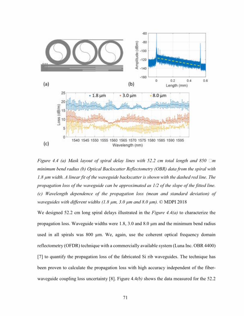
71
Figure 4.4 (a) Mask layout of spiral delay lines with 52.2 cm total length and 850 m
minimum bend radius (b) Optical Backscatter Reflectometry (OBR) data from the spiral with
1.8 µm width. A linear fit of the waveguide backscatter is shown with the dashed red line. The
propagation loss of the waveguide can be approximated as 1/2 of the slope of the fitted line.
(c) Wavelength dependence of the propagation loss (mean and standard deviation) of
waveguides with different widths (1.8 µm, 3.0 µm and 8.0 µm). © MDPI 2018
We designed 52.2 cm long spiral delays illustrated in the Figure 4.4(a) to characterize the
propagation loss. Waveguide widths were 1.8, 3.0 and 8.0 µm and the minimum bend radius
used in all spirals was 800 µm. We, again, use the coherent optical frequency domain
reflectometry (OFDR) technique with a commercially available system (Luna Inc. OBR 4400)
[7] to quantify the propagation loss of the fabricated Si rib waveguides. The technique has
been proven to calculate the propagation loss with high accuracy independent of the fiber-
waveguide coupling loss uncertainty [8]. Figure 4.4(b) shows the data measured for the 52.2

72
cm long spiral of 1.8 µm wide ULL silicon waveguide. The peaks on the left-hand side (near
0 m distance) and right-hand side (near 0.5 m distance) are the reflections at the waveguide
facets. The linearity of the trace verifies that the waveguide loss is not bend-loss limited. The
measured mean and deviation of spectral dependence of the propagation loss of the three
waveguide widths are plotted in Figure 4.4(c). A single mode 1.8 µm wide waveguide
achieves an average of 16 dB/m propagation loss over the C+L band. The propagation loss in
multimode ULL waveguide with 3.0 µm and 8.0 µm widths are lower, at 10 dB/m and 4 dB/m
respectively.
The measured loss of the ULL waveguides show a relatively large discrepancy to the values
predicted by the nw approximation method described in Section 2.2 (Figure 4.4(b)). The model
made several simplifications such as ignoring the surface roughness of the etched slab
surfaces. For fully etched (500 nm) or halfway etched (231 nm) waveguides, the optical field
that interacts with the etched surface is small enough to be neglected in the total loss
calculation. However, with the very shallow rib (56 nm) waveguides the optical field expands
laterally (similar to a slab mode) and the interaction between the mode field and the etched
surface cannot be ignored. The roughness rms of the etched surface is typically on order of
several nanometers, which is more than one order of magnitude larger than the unetched
waveguide top surface roughness (~0.1 nm). The scattering due to the etched surface
roughness is significant and results in the discrepancy between the experimental and
theoretical waveguide loss.

73
4.2 Ultralow loss passive component demonstrations
We utilize these ULL silicon waveguides to successfully demonstrate high quality-factor (Q)
ring resonators and low kappa (κ), narrow bandwidth Bragg grating reflectors with record
performance for sub-micron SOI waveguides.
4.2.1 High quality-factor ring resonators
One key component made possible by low-loss waveguides is the high-Q ring resonator. Ring
resonators are an essential building block to realize compact optical filters and delays on chip.
Higher Q-factors enable sharper, narrowband filters and longer delays, which are
requirements for the aforementioned ultra-long laser cavity. There has been a plethora of
recent work to demonstrate high-Q integrated resonators using different materials and cavity
geometries. These results include fully integrated resonators with an intrinsic Q of 22 million
in silicon [9], 81 million in a silicon nitride resonator [10] and over 200 million in a silica
resonator [11]. However, the latter two results are multimoded, which can lead to multiple
sets of resonances or excess loss at the coupling regions unless special care is taken to optimize
the coupler [12]. These three results all have bend radii > 2mm, which limits the compactness
of the device and complicates the design of a Vernier-effect filter due to the small free spectral
range of each ring. Finally, it is unlikely that these resonators were designed with laser
integration in mind, and cannot be integrated with the heterogeneous silicon/III-V laser
without significant extra processing [13], [14].
In this work, we demonstrate ring resonators readily integrable with the heterogenous
silicon/III-V platform with a loaded Q of 2.1 million, and an intrinsic Q of 4.1 million. The
ring is in an all-pass configuration, and is 1.8 microns in width, which is single-mode for the
TE polarization. The ring is connected to a bus waveguide of the same dimensions using a

74
straight-to-curved coupler with a 1.2 micron coupling gap. The transmission spectra of the
ring are measured by sweeping a high-resolution tunable laser (0.1 pm steps) across the
resonance and measuring the output power. The resulting spectra is depicted in Figure 4.5(a)
and fitted with a Lorentzian function. The measured full width half max (FWHM) is 91.3MHz.
Figure 4.5. (a) Measured spectral responses of the 750 µm radius Si ring resonator (all-pass
configuration) plotted with a Lorentzian fit. The extracted intrinsic quality factor Qint = 4.1
million. (b) Simulated bend-loss limited intrinsic Q of the rings versus ring radius at three
etch depths. The experimental data of the targeted 56 nm etch depth are depicted as blue
circular markers. © MDPI 2018
The ring in Figure 4.5(a) has a 750 µm bend radius, for which we did not observe any bend-
loss induced radiation in the resonator. To confirm this, we investigated rings with varying
radii, and plot their intrinsic Q factor alongside the theoretical bend-loss limit for Q in Figure
4.5(b). The experimental results are extracted from the measured FWHM, while the dashed
lines are simulated using a commercial mode solver. The simulations are shown for three
different etch depths, as that is the most sensitive parameter to the bend-loss. We find that our
ring in this experiment is a bit over etched compared the target 56 nm, judging by the Q of the
smaller rings. We do not observe significant bend loss in the rings until the radius is less than

75
550 mm. For practical reasons, the ring radius should be larger than 600 mm to avoid bend-
loss possibly caused by an underetch of the waveguide.
4.2.2 Narrow bandwidth Bragg gratings
Another useful component that can be realized with low-loss waveguides is a low-kappa ()
Bragg grating. These gratings are widely used in filters, sensors, and semiconductor lasers as
a wavelength selective element, much like the ring resonator. The bandwidth of the grating is
directly proportional to power coupling coefficient , and therefore can be minimized by
reducing the perturbation strength of the grating [15]. At the same time, the length (L) of the
grating should be long enough (L ~ 1) and the loss of the waveguide must be low in order to
obtain sufficient reflection. Care must be taken in the design of the grating in order to achieve
weak as conventional sidewall or top surface gratings tend to have stronger . Instead, we
utilize “post” (or inversely, “hole”) gratings in which small areas of the waveguiding material
are placed (removed) periodically on either side of the waveguide. The dimensions of the
posts (holes) and proximity to the waveguide can be lithographically defined and tailored to
achieve the desired . This approach has been successful for low loss silicon nitride gratings
[16]. For our waveguides, it is simpler to etch holes on either side of the waveguide, as shown
in Figure 4.6(a). The resulting of the grating is directly controlled by the hole-to-waveguide
distance, while the period of the grating is set to be 240 nm, corresponding to a stopband at
1563 nm for an unperturbed waveguide neff = 3.2560.
We fabricate uniform gratings with lengths of 0.5 and 1.0 cm. The waveguide width is 1.8
µm, and the length is 2.2 cm. We used an e-beam lithography to write the grating teeth,
although DUV immersion lithography can also resolve 120 nm features. Transmission and
reflection spectra are measured and fitted using transfer matrix modeling. This approach also

76
accounts for Fabry-Perot cavities formed by the waveguide facets, which affects the grating
shape. From this, we extract the bandwidth and peak reflectivity of the grating, which can then
be used to estimate . A few selected gratings are depicted in Figure 4.6(b) along with the
predicted grating bandwidth. Using 1 cm long gratings, we were able to achieve a 50 pm
FWHM bandwidth with roughly 70% reflectivity, with potential to further reduce the
bandwidth with a longer grating.
Figure 4.6 (a) An SEM image of the fabricated low Bragg grating waveguide with a close-
up of the holes on both sides of the waveguide. (b) Theoretical calculations of gratings’ full
width half max (FWHM) versus varying L for 0.5, 1 and 2 cm long grating waveguides.
Circular blue markers show the measured data. (c-d) Spectra of reflection and transmission
of 1 cm long grating waveguides with κ=1.25 cm-1 and κ=4.0 cm-1, respectively. The ripples
are caused by reflections off the waveguide facets. (e) The extracted n, and exponential
fit as a function of waveguide to hole distance. © MDPI 2018
4.3 Bridging ultralow loss to standard silicon waveguides
A low loss taper to transition from ULL waveguides to a waveguide geometry with smaller
bend radius is the key for adding the ultralow loss passive devices into the heterogeneous
Si/III-V platform. This allows us to basically expand the versatility of the heterogeneous
silicon platform and, most importantly in the scope of this dissertation, allows for lowering
the frequency noise of the lasers by orders of magnitude.

77
Figure 4.7 shows the schematic of an adiabatic taper for a low loss, low reflection transition
of the optical mode from the 56 nm etched rib ULL waveguide to the standard 231 nm etched
rib waveguide, which has a smaller critical bend radius (40 µm). The waveguide width is set
at 1.8 µm. The mode transition happens along the linear taper formed by etching on the Si
slab. Figure 4.7 (a-c) shows the simulated profiles of the waveguide’s fundamental mode at
points a, b and c denoted on the schematic figure.
Figure 4.7 Schematic of the taper converting the optical mode from an ULL waveguide to
standard rib (231 nm etch-depth) waveguide. Figures (a), (b) and (c) show the waveguide
mode profiles at locations labeled a – ULL silicon waveguide, b – central part of the taper,
and c - standard silicon waveguide along the taper structure. © MDPI 2018
In order to ensure an adiabatic transition from fundamental mode of the 56 nm etched
waveguide to the 231 nm etched waveguide, the length of the linear taper must be sufficiently
long. As shown in Figure 4.8(a), at 1550 nm wavelength, high order modes in the deeper rib

78
waveguide are excited if the taper length is shorter than 25 µm. With a taper longer than 50
µm, both mode expansion and FDTD simulations show that essentially 100% transmission in
the fundamental mode is achieved. The reflection power is also simulated and is shown to be
lower than -60 dB level. To be safe, the taper length of 200 µm is chosen in practice. The
wavelength dependence of the transmission efficiency and reflection power are again
simulated in FDTD and shown in Figure 4.8(b). Larger than 99.8% transmission and lower
than -55 dB reflection should be achievable over the whole C+L band.
Figure 4.8 (a) Simulation results at 1550 nm wavelength of the optical transmissions and
reflections at the deep-shallow taper. The fundamental mode was launched from the ULL
silicon waveguide side. Transmitted and reflected powers to the fundamental mode and high
order modes were simulated using two methods. The solid lines show the results using mode
expansion simulation, while the markers are the data points simulated with FDTD (b)
Wavelength dependence of the transmission and reflection from fundamental input mode to
fundamental output mode, simulated with FDTD. © MDPI 2018
4.4 Summary
In this chapter, we have successfully developed and accomplished a new type of silicon
waveguides with ultralow propagation loss. The waveguides use a shallow (56 nm) rib
geometry and can be seamlessly integrated into our standard heterogeneous silicon/III-V

79
active components such as lasers, modulators, and photodetectors. Waveguide loss is as low
as 0.04 dB/cm for a multimode waveguide and 0.16 dB/cm for a quasi-single mode waveguide.
This low loss performance results in record high-Q ring resonators and narrowband grating-
based filters. We have demonstrated ring resonators with 4.1 million intrinsic Q, and ultra-
narrow band Bragg gratings, which are essential to achieve ~100 Hz level linewidth lasers on
silicon. Finally, we show a simple way to bridge this ultralow loss waveguide to the standard
waveguide using a taper design with negligible insertion loss.

80
References
[1] T. Komljenovic and J. E. Bowers, “Monolithically Integrated High- Rings for Narrow
Linewidth Widely Tunable Lasers,” IEEE J. Quantum Electron., vol. 51, no. 11, pp. 1–
10, 2015.
[2] D. Melati, A. Melloni, and F. Morichetti, “Real photonic waveguides: guiding light
through imperfections,” Adv. Opt. Photonics, vol. 6, no. 2, p. 156, Jun. 2014.
[3] D. Melati, F. Morichetti, and A. Melloni, “A unified approach for radiative losses and
backscattering in optical waveguides,” J. Opt. (United Kingdom), vol. 16, no. 5, p.
055502, 2014.
[4] M. L. Davenport, S. Liu, and J. E. Bowers, “Integrated heterogeneous silicon / III – V
mode-locked lasers,” Photonics Res., vol. 6, no. 5, pp. 468–478, 2018.
[5] M. A. Tran, T. Komljenovic, J. C. Hulme, M. Kennedy, D. J. Blumenthal, and J. E.
Bowers, “Integrated optical driver for interferometric optical gyroscopes,” Opt.
Express, vol. 4, no. 4, pp. 3826–3840, 2017.
[6] C. Zhang, S. Zhang, J. D. Peters, and J. E. Bowers, “8 × 8 × 40 Gbps fully integrated
silicon photonic network on chip,” Optica, vol. 3, no. 7, p. 785, 2016.
[7] B. J. Soller, D. K. Gifford, M. S. Wolfe, and M. E. Froggatt, “High resolution optical
frequency domain reflectometry for characterization of components and assemblies.”
[8] J. F. Bauters et al., “Planar waveguides with less than 0.1 dB/m propagation loss
fabricated with wafer bonding.,” Opt. Express, vol. 19, no. 24, pp. 24090–101, Nov.
2011.
[9] A. Biberman, M. J. Shaw, E. Timurdogan, J. B. Wright, and M. R. Watts, “Ultralow-
Loss Silicon Ring Resonators,” vol. 37, no. 20, pp. 4236–4238, 2012.

81
[10] D. T. Spencer, Y. Tang, J. F. Bauters, M. J. R. Heck, and J. E. Bowers, “Integrated Si
3 N 4 / SiO 2 Ultra High Q Ring Resonators,” vol. 4, pp. 141–142, 2012.
[11] K. Y. Yang et al., “Bridging ultrahigh-Q devices and photonic circuits,” Nat.
Photonics, vol. 12, no. 5, pp. 297–302, May 2018.
[12] M. H. P. Pfeiffer, J. Liu, M. Geiselmann, and T. J. Kippenberg, “Coupling Ideality of
Integrated Planar High- Q Microresonators,” Phys. Rev. Appl., vol. 7, no. 2, p. 024026,
Feb. 2017.
[13] M. Davenport, J. Bauters, M. Piels, A. Chen, A. Fang, and J. E. Bowers, “A 400 Gb/s
WDM Receiver Using a Low Loss Silicon Nitride AWG Integrated with Hybrid Silicon
Photodetectors,” Opt. Fiber Commun. Conf. Fiber Opt. Eng. Conf. 2013, p. PDP5C.5,
2013.
[14] M. L. Davenport and J. E. Bowers, “Efficient and broad band coupling between silicon
and ultra-low-loss silicon nitride waveguides,” in 2016 IEEE Photonics Conference
(IPC), 2016, pp. 631–632.
[15] M. Poulin et al., “Ultra-narrowband fiber Bragg gratings for laser linewidth reduction
and RF filtering,” 2010, vol. 7579, p. 75791C.
[16] D. T. Spencer, M. Davenport, S. Srinivasan, J. Khurgin, P. A. Morton, and J. E. Bowers,
“Low kappa, narrow bandwidth Si_3N_4 Bragg gratings,” Opt. Express, vol. 23, no.
23, p. 30329, 2015.

82
Chapter 5. Ultralow Noise Widely Tunable Lasers
This chapter presents ultralow noise lasers (140 Hz fundamental linewidth) with ultrawide
wavelength tuning range (up to 120 nm). These record-breaking performances are achievable
only with the incorporation of the ultralow loss silicon waveguides developed in chapter 4.
The laser structural concept is shown in Figure 5.1. The laser utilizes the ultralow loss high
Q ring resonators (56 nm etch-depth) in the extended cavity (multiring mirrors) for linewidth
narrowing. The standard Si waveguides (231 nm etch-depth) are used elsewhere for a high
gain performance Si/III-V in the active section and for small footprint in the passive
components (e.g. couplers, small loop mirror, phase shifters).
Figure 5.1 Conceptual illustration of the ultralow noise tunable laser integrated on Si/III-V.
5.1 Laser Designs
The structure of the lasers is similar to that of the dual-ring mirror laser presented in chapter
3 with some necessary modifications to suit for the desired ultrawide tunability. The schematic

83
designs of the lasers with triple-ring mirror and quad-ring mirror are illustrated in Figure
2.1(a) and (b) respectively.
Figure 5.2 Schematic of tunable lasers. The front-mirror is a tunable-mirror formed with an
MZI tunable directional coupler. Gain section is an optical amplifier heterogeneous Si/III-V
waveguide, connected to the Si passive waveguides via two Si/III-V tapers. The phase tuner
is a microheater on the top cladding of the Si waveguide. The back-mirror is a multiring
mirror with, (a) three rings, (b) four rings, and a tunable coupler. 231 nm etch Si waveguides
are drawn in black while 56 nm etch Si waveguides are in blue.
Key components are listed below:
(a) Front tunable-mirror (low reflective mirror): The front-side loop mirror formed by
looping the two ports of a tunable MZI directional coupler. Since the reflectivity is
adjustable for any wavelength, we can achieve the optimal point over the whole ~120
nm span. The rib Si waveguide is 231 nm etched from the 500 nm thick Si layer
(b) A single-sectioned optical amplifier Si/III-V waveguide (gain section): We keep the
same design of the amplifier waveguides used previously in Chapter 3 but the length

84
of this active element is made 2.5 mm long to scale up with the total cavity length
design.
(c) Phase tuner: A long metal (Ti/Pt) strip is deposited vertically on the top of the oxide
cladding of the Si waveguide to form the microheater for phase tuning using the
thermo-refractive effect.
(d) Multiring mirrors: The back-side mirror of the laser is a multiring mirror structure
formed by a tunable coupler and three ring resonators - as in triple-ring mirror design,
or four ring resonators - as in quad-ring mirror design, cascaded in a loop in add-drop
configurations. The ring resonators are all 56 nm etched Si rib waveguides (therefore
sketched in different color from the rest in Figure 5.2. The designs of these multiring
mirrors are the focus of the sub-sections that follow.
5.1.1 Ring resonators
The geometry of the ultralow loss waveguides used for the ring resonators should be single-
mode for good laser operation. From the mode analysis shown (see chapter 4), a waveguide
width of 1.8 µm and 56 nm etch-depth rib is chosen to meet that requirement. From the
experiment results in chapter 4, the waveguide loss was measured to be lower than 0.16 dB/cm
across the C+L bands and minimum bend radius is about 600 µm. Similar to the
implementation in chapter 3, we also design the ring resonators here in the simple
configuration of a circular ring closed to a straight bus waveguide (Figure 5.3(a)). The power
cross coupling ratio between the bus and the ring is simulated using the eigen-mode expansion
and CMT methods. A sweep of the two key parameters, ring radius and gap, were carried out
to obtain a two-dimensional map shown in Figure 5.3(b). The map is convenient for the
designer to look up for appropriate pairs of parameter values for desired coupling ratios.

85
Figure 5.3 (a) Schematic of the ring-bus coupler structure for simulation. (b) Power cross
coupling ratio as a function of the ring radius and the gap between the ring and bus
waveguide.
5.1.2 Multiring mirrors
One immediate downside of the ultralow loss waveguides is their large bend radius, which is
almost 10x larger than that of the standard Si waveguides. The large radius results in a small
FSR of the ring and renders the dual-ring mirror incapable of providing sufficient side-mode-
suppression-ratio (SMSR) for stable single mode lasing. To see this, Figure 5.4 shows the
reflection spectrum of a dual-ring mirror with ring radii of 599.97 and 600.86 µm, and power
coupling ratios all equal to 0.09. The spectrum is very dense when looking at wide wavelength
span (Figure 5.4(a)) due to the individual ring’s ring FSR. When zooming in as in Figure
5.4(b), we could see many strong resonant modes closed to each other. That is not good for
our single frequency laser design.

86
Figure 5.4 Reflection spectrum of dual-ring mirror structure with large bend radii (~600 µm)
shows low side mode suppression ratio. Plot (b) is the close-up of (a).
To overcome this issue, we need to enhance the SMSR by having more filtering elements.
Here, we do that by the addition of more ring resonators, i.e. multiring mirrors with three and
four ring resonators, as illustrated in Figure 3.2(a, b).
Figure 5.5 Generic configuration of (a) triple-ring mirror (b) quad-ring mirror.
Multiring mirrors are simply the extension of the dual-ring mirror configuration presented in
Chapter 3. The Vernier FSR, which sets the tuning span of the tunable lasers, is determined
by the first two rings, so-called the Vernier rings. The radii of the third and the fourth ring (if

87
applicable) would be chosen appropriately to achieve the maximum side mode suppression
effect.
For spectral analysis, we come back to the analytical results for multiring ring mirrors derived
in Appendix 1. The bus-ring coupling ratios for each ring, ring radius and amplitude
propagation loss constant are denoted by , ,m m mR (m =1, 4 ). For triple- and quad-ring
mirror structures as shown in Figure 5.5 where the coupling ratios for add and drop are the
same on each ring, the complex amplitude reflectivity of the mirrors is given by
4
2 2
1
2 1 , , ,mirror c c drop m m m pm
r j t R
(5.16)
1/2 2 /22
22
2, , ,
1 1 2
m p
m p
j R
m m p
drop m m m p j R
m m p
R et R
R e
(5.17)
where p is the effective propagation constant in the waveguide and the subscript m stands
for the ring resonators.
Table 5.1 Multi-ring mirror design parameters
Mirror design 2 R1 (µm) R2 (µm) R3 (µm) R4 (µm) Vernier FSR (nm)
Triple-ring 0.09 599.97 600.86 707.57 - 113.9
Quad-ring 0.16 599.97 600.79 711.6 849.43 123.4
Upon all considerations, our chosen designs for triple-ring mirror and quad-ring mirror are
listed in Table 5.1. Within each mirror, the power cross coupling ratios at all the ring resonators
are chosen to be the same value ( 2 ). The spectral responses of the triple-ring mirror are
shown in Figure 5.6, where a broad reflection spectrum and a close-in spectrum are plotted.
The broad spectrum (Figure 5.6(a)) shows us a ~114 nm Vernier FSR, while the close-in
spectrum (Figure 5.6(b)) reveals how effectively the third ring resonator helps suppress the

88
sidemodes. As a result, an SMSR over the whole span of > 8dB is achieved, a substantial
improvement from what we got with only the two Vernier rings (as in Figure 5.4(b)).
Figure 5.6 Reflection spectra of the triple-ring mirror (a) Broad spectrum shows the
wavelength response across two Vernier FSRs (b) Close-in spectrum shows the sidemodes
near the central reflection resonance peak with SMSR >8 dB.
For the quad-ring mirror, the addition of two more ring resonators provides more capability
to engineer the mirror wavelength response. As shown in the Figure 5.7, higher (>16 dB)
SMSR can be achieved even with the higher power coupling ratios ( 2 0.16 ) than the triple-
ring mirror. This means resonators in quad-ring mirror can have lower Q than that in the triple-
ring mirror to obtain equivalent performance. The price for this additional advantage is,
obviously, the increase in the total foot print and the addition of one more control element
needed for resonance alignment. The calculated designed FSR is about ~123 nm.

89
Figure 5.7 Reflection spectra of the quad-ring mirror (a) Broad spectrum shows the
wavelength response across two Vernier FSRs (b) Close-in spectrum shows the sidemodes
near the central reflection resonance peak with SMSR >16 dB.
Finally, Figure 5.8 plots the laser’s effective cavity length calculated for the case of (a) triple-
ring mirror and (b) quad-ring mirror. Both mirrors result in very long cavity length (>50 mm),
which would provide a highly coherent laser field.
Figure 5.8 Effective cavity length of the laser with (a) the triple-ring mirror (b) the quad-ring
mirror.

90
5.1.3 Laser linewidth simulation
We reuse the modeling and approximation method previously used in chapter 3. The list of
parameters is shown in Table 5.2; most of these parameters are identical to what were used in
Chapter 3 with changes in bold.
Table 5.2 List of parameters used for laser linewidth calculations
Parameter Symbol Value Unit
Wavelength 1.575 µm
Planck constant h 6.62607004 × 10⁻³⁴ m2kg / s
Light velocity c 299792458 m/s
Optical frequency /c Hz
Mode’s group index gn 3.8/3.61
Mode’s group velocity gv / gc n cm/s
Spontaneous emission factor spn 1.5
Linewidth enhancement factor H 4
Gain section internal loss i 6 cm-1
Si waveguide loss p 0.16 dB/cm
III-V/Si taper loss dBtaper 0.5 dB
Gain length La 2.5 mm
Routing waveguide total length Lp 2 mm
Output Power P0 10 mW
The estimated values of A, B, and F and the modified Schawlow-Townes linewidth as
functions of the frequency detuning from the resonance peak frequency are then calculated
for the two designs (revisit the laser simulation section in Chapter 3 for details), with the
output power assumed to be 10 mW. Both designs show achievable linewidths in 10s of Hz

91
level, in theory. This is two order of magnitude improvement in linewidth from the results
achieved with dual-ring mirror using higher loss Si waveguides in chapter 3.
Figure 5.9 Calculated values for coefficients A, B and F and estimated Lorentzian linewidth
as functions of frequency detuned from the reflection peak resonance for a laser output power
of 10 mW. Values of parameters used for these calculations are listed in Table 5.1 and Table
5.2. Figures (a-b) are of the triple-ring mirror laser and (c-d) are of the quad-ring mirror
laser.
5.2 Laser fabrication
The designed laser is then fabricated in a modified version of Si/III-V heterogeneous process.
Some modification was necessary, including the self-aligned process for etching Si
waveguides for zero-misalignment in the transition between 56 nm and 231 nm etch-depths,

92
and the selective bonding process to preserve the ultralow loss Si waveguide area from III-V
bonding. The fabrication process flow can be found in Appendix 3. Stitched microscopic
images of completed devices are shown in Figure 5.10(a) and (b). SEM images of the self-
aligned transition between two types of Si waveguides and Si/III-V taper are also shown in
the insets (i) and (ii). The facets of the lasers were mechanically polished for fiber coupling.
Figure 5.10 (a) Microscopic images of a fabricated triple-ring mirror laser (b) Microscopic
images of a fabricated triple-ring mirror laser. (i) SEM image of a Si/III-V taper. (ii) SEM
image of a transition from 56 nm to 231 nm etched waveguides.
Unfortunately, right after the fabrication is completed, the lasers had an extremely high
contact resistivity due to some unclear fabrication issues. Very small amount of current could
barely flow despite high bias voltage. The diode electrical property was notably remedied after
an additional rapid-thermal-annealing, and then improved to an acceptable level after tens of
minutes of continuous burn-in process, i.e. when a fixed current was forced to flow through
the diode, the bias voltage gradually reduces until saturates. These issues possibly relate to 1)
hydrogen contamination happened during some dry etching and oxide deposition processes

93
that contain hydrogen gas [11], and 2) bad interface between contact metal and semiconductor.
Future work should definitely address this issue to achieve lasers with better performance.
5.3 Laser characterization
The lasers were measured on a temperature-controlled stage set at 20°C. The output light is
coupled into a 2.5 µm spot-size lensed fiber for characterization of spectral properties such as
wavelength tuning, spectral linewidth and frequency noise. A Faraday based in-line optical
isolator with larger than 50 dB extinction ratio was connected to the lenses fiber to eliminate
any unintentional reflections towards the laser. The current-voltage curve of the lasers are
shown in Figure 5.11(a), while the current-output power curve for the triple-ring mirror laser
is shown in Figure 5.11(b). The left y-axis in Figure 5.11(b) shows the lasing wavelength at
each current point. At each point the rings and phase section were tuned to obtain the
maximum power, but the wavelength shifted quite a bit due to the thermal crosstalk between
the active sections and the rings, and that resulted in the non-smooth L-I curve. The laser’s
threshold current was about 100 mA. The max output power was only ~3 mW, which is ~3.3
times lower than the values used for the linewidth calculations in the previous section.

94
Figure 5.11 (a) Current-voltage relation of the 2.5 mm long gain section (b) The light-current
curve of the triple-ring laser. The lasing wavelength was not kept constant across the current
sweeping, shown in the right y-axis.
5.3.1 Wavelength tuning
We tested the laser wavelength tuning at a fixed injection current of 300 mA (~3x threshold
current) to the gain section of the laser. The lasing spectra are acquired by a grating-based
optical spectrum analyzer. An initial coarse tuning was done to acquire the lasing spectra
across the tuning range and followed by a two-dimensional sweep of ring fine tunings to obtain
the full tuning map for the laser. In our test procedure, the electrical powers applied to the
heaters on top of two ring main Vernier resonators are stepped. For each operation point, the
power applied to the heaters on top of the remaining ring resonators, phase section and the
tunable couplers is was tuned to achieve the maximum output power indicated by the
photocurrent read-out on the on-chip monitor photodiode. Because of thermal crosstalk
between elements, it was necessary to run several tuning optimization cycles for each
operation point. The measurement was automated by a computer program. The lasing spectra
at different pair values of heater powers on two rings are recorded and post-processed for our
analysis.
Results for the triple-ring mirror laser is shown in. The course tuning in Figure 5.12 (a) shows
a 110 nm wide wavelength tuning from 1490 nm to 1600 nm. This is in good agreement with
the designed Vernier FSR of ~113 nm (see Table 5.1). A linear and smooth 2D wavelength
tuning map is achieved, as shown in Figure 5.12(b). The corresponding SMSR map is shown
in Figure 5.12(c). SMSRs on almost all of lasing points are within the range 40 ~55 dB, even
at wavelength far off from the SOA’s gain spectrum peak (~1550 nm). The variation on the

95
SMSR originates from how well the two ring spectra are aligned to each other at the pre-
determined heater setpoints in the test.
Figure 5.12 Tuning characteristic of the triple-ring mirror laser: (a) Course tuning spectra
showing the tuning range of 110 nm (b) Two-dimensional wavelength tuning map of the dual-
ring mirror laser. The color indicates the lasing wavelength in unit of nm. (c) Side-mode
suppression ratio (SMSR) of the corresponding wavelength tuning map, showing >40 dB on
most of the operation points.
Results for the quad-ring mirror laser is shown in Figure 5.13. Unfortunately, due to issues
with electrical contact and for some unknown reasons, the gain spectrum had degraded quickly
after operating for a short duration. The gain spectrum shape distorted after the degradation.
Although we could still have lasing, the laser power was dropped by 10-15 dB. Despite all of
those problem, the coarse tuning in Figure 5.13(a) still shows a 120 nm wide wavelength
tuning from 1484 nm to 1604 nm, which is close to the designed 123 nm Vernier FSR (see

96
Table 5.1). The 2D wavelength tuning map is shown in Figure 5.13 (b) and the corresponding
SMSR map is shown in Figure 5.13 (c). The tuning map is more erratic than that of the triple-
ring mirror laser, partially from the additional difficulty of having one more sensitive ring that
needed to be tuned and the thermal crosstalk between many tuning elements. A more advanced
tuning algorithm might be helpful in improving the wavelength tuning performance of the
laser.
Figure 5.13 Tuning characteristic of the fabricated quad-ring mirror laser: (a) Course tuning
spectra showing the tuning range of 120 nm (b) Two-dimensional wavelength tuning map of
the dual-ring mirror laser. (c) Side-mode suppression ratio (SMSR) of the corresponding
wavelength tuning map.

97
5.3.2 Frequency noise and linewidth
We measured the laser’s frequency noise to characterize the linewidth of interest. Due to the
availability of the testing tools at the time, the triple-ring mirror laser was measured with a
Sycatus/Ogmentum phase noise measurement system [1], which has 20 MHz bandwidth,
while the quad-ring mirror laser was tested with a measurement system provided by OEWaves
[2] which extends up to 100 MHz.
Figure 5.14 (a) Frequency noise spectrum of the fabricated triple-ring mirror laser measured
at 300 mA. (b) The same spectrum plotted with x-axis in linear scale to zoom-in on the noise
at high frequency range. An upper bound of 70 Hz2/Hz for the white noise level is drawn.
The one-sided spectrum of frequency noise power spectral density of the fabricated triple-ring
mirror laser is shown in Figure 5.14. The measurement was taken at 300 mA pump current
and slightly detuned from the peak resonance of 1545 nm wavelength. Despite using all
battery powered current sources isolated from power lines, there is still significant
contribution to the measurement from other sources in the 10kHz to 10MHz range. The
frequency noise spectrum seems to have not fully reached its white noise level within 20 MHz
measurement bandwidth. Therefore, we deem 70 Hz2/Hz as the upper-bound of the laser’s

98
white noise level. It is equivalent to state that the Lorentzian linewidth of the fabricated triple-
ring mirror is lower than 220 Hz [3].
The frequency noise of the quad-ring mirror laser was tested, fortunately, before the
catastrophic degradation happened, at 1565 nm wavelength and output power of about 2 mW.
The one-sided spectrum of frequency noise power spectral density is shown in Figure 5.15.
The spectrum was somewhat hindered by the spikes at 18 MHz and harmonics, which are the
frequency fringes corresponding to the free spectral range of the fiber MZI used in the
measurement system. However, it is possible to observe the laser’s true noise behavior outside
the spike areas. We could see that the laser frequency noise is still dominated by colored noise
up to 35 MHz level. A white noise level of 45 Hz2/Hz starts to be seen at about 60 -80 MHz
frequency range. That corresponds to a Lorentzian linewidth of 140 Hz.
Note that the factor of 5.5 times difference between this measured linewidth of the quad-ring
laser with the predicted linewidth (~25 Hz) in Figure 5.9(d) in section 5.1.3 is largely due to
the fact that the measured output power (2 mW) is 5 times lower than the assumed output
power for the calculation (10 mW). This justifies the result discrepancy because the laser
linewidth is inversely proportional to output power level.

99
Figure 5.15. (a) Frequency noise spectrum of the fabricated quad-ring mirror laser. (b) The
same spectrum plotted with x-axis in linear scale to zoom-in on the noise at high frequency
range. The spikes at 18 MHz and harmonics are from the measurement tool. A white noise
level of 45 Hz2/Hz is drawn.
5.4 Summary
This chapter described the design, theoretical calculation, fabrication and characterization of
heterogeneously integrated Si/III-V lasers using triple-ring and quad-ring mirrors. Both lasers
exhibit ultrawide tuning range of 110 nm on the triple-ring and 120 nm on the quad-ring mirror
lasers, which is in great compliance with the design.
In term of spectral linewidth, the lasers were expected to achieve 10s Hz linewidth level, but
the best linewidth measured experimentally is 140 Hz on the quad-ring mirror laser. The triple-
ring mirror laser’s linewidth was measured to be lower than 220 Hz, although a conclusive
linewidth measurement was not possible due to the measurement tool’s limit.

100
References
[1] “Optical Noise Analyzer.” [Online]. Available:
http://www.sycatus.com/en/products/ona/. [Accessed: 17-Mar-2019].
[2] “HI-Q Optical TMS | OEwaves.” [Online]. Available: https://oewaves.com/hi-q-
optical-tms. [Accessed: 13-Mar-2019].
[3] K. Kikuchi and T. Okoshi, “Estimation of Linewidth Enhancement Factor of AlGaAs
Lasers by Correlation Measurement Between FM and AM Noises,” IEEE J. Quantum
Electron., vol. 21, no. 6, pp. 669–673, 1985.

101
Chapter 6. Ultralow Noise Extended-DBR Lasers
In this chapter, we present the designs and characteristics of fixed wavelength DBR lasers.
The so-called Extended-DBR lasers are created by incorporating centimeter-long weak Bragg
grating (first demonstrated in Chapter 4) into a part of the laser cavity. The laser architectural
concept is shown in Figure 6.1. The E-DBR laser shows linewidth lower than 1 kHz. By
adding a high-Q ring resonator in cascade with the gratings, the spectral linewidth is lowered
to ~500 Hz level on the Ring-Assisted Extended-DBR laser.
Figure 6.1 Concept of the ultralow noise extended-DBR laser on Si/III-V integrated platform.
6.1 Laser Designs
The requirements to fabricate a Bragg grating with long length and narrow bandwidth are low
propagation loss and sufficiently weak perturbations, i.e. low . This is depicted in Figure
6.2, in which the bandwidth and reflectivity of a uniform grating are simulated. Weakening

102
the grating decreases the full-width half maximum (FWHM) of the grating and lowers the
reflectivity. For the same L, a longer grating will provide an even narrower passband, but is
more sensitive to the optical loss, which also decreases the reflectivity and increases mirror
loss. Thus, both weak κ and low waveguide loss are needed to achieve a narrowband grating
reflector with enough reflectivity. For E-DBR lasers, we target grating strengths with L < 1,
and optical losses less than 0.2dB/cm, both of which are achievable using the ULL silicon
platform.
Figure 6.2 Impact of grating strength on the (a) full-width half maximum (FWHM) bandwidth
and (b) reflected power assuming a 15mm long uniform grating. The simulations are shown
over various lengths and waveguide losses.
For conventional sidewall or surface etched gratings, the power coupling coefficient is
directly proportional to the perturbation in waveguide width or height respectively. These
perturbations become too small to resolve in device fabrication in the limit that approaches
zero. Alternate grating designs to achieve ultra-low were demonstrated for ULL Si3N4
waveguides, including etched pillars set back from the waveguide, sampled gratings and
higher order gratings [1]. As first demonstrated in chapter 5, ULL shallow etched silicon
waveguides utilizes periodically etched holes through the silicon layer on either side of the
waveguide to achieve the same low values. In this design, is inversely proportional to the

103
distance between the holes and the waveguide, which can be well controlled with lithography.
The dependence between this distance and was previously simulated and experimentally
verified [2]. Finally, the other component enabled by the ULL Si platform is the high-Q ring
resonator, which was demonstrated to be as high as 4.1 million for intrinsic Q and 2.1 million
for loaded Q. Using a high-Q ring in the laser cavity can serve to further reduce the linewidth,
as it provides enhanced cavity length near resonance and sharpens the cavity filter, as we have
seen in the previous chapters.
Figure 6.3 (a) Schematic of the E-DBR laser. A ring resonator is incorporated in the cavity
(b) to form the RAE-DBR laser.
The two laser designs detailed in this work are shown in Figure 6.3; the Extended-DBR (E-
DBR) laser and Ring-Assisted E-DBR (RAE-DBR) laser. The lasers include a tunable back
mirror, a III-V on silicon gain section, a phase control section, and a long Bragg grating-based
front mirror through which the light is output. The RAE-DBR laser has an additional ring

104
filter as part of the laser cavity to increase the effective cavity length and reduce the reflector
sidelobes.
The gain section is the same for the two lasers and consists of InAlGaAs multiple quantum
well (MQW) material with 3 quantum wells [3]. The length of the gain section is 2.5mm, and
it is connected to the ULL silicon waveguides and gratings through two tapered transitions, as
shown in Figure 6.3(a). Each laser also includes a phase control section that can be tuned to
align the lasing mode to the reflector peak. The tuning in the laser is achieved via thermal
tuning by heating up a metallic resistor located on top of each element. There are no heaters
on top of the grating, but one could be included to provide some tunability of the Bragg
wavelength. The heaters are separated from the optical waveguide layers by 1m of sputtered
oxide cladding, which is sufficient to avoid any absorption loss by the metal.
The back mirror of the lasers is a tunable reflector consisting of a Mach-Zehnder
interferometer (MZI) with a loop mirror. The reflectivity of the mirror can be varied from zero
to 4s(1-s), where s is the power splitting ratio of the couplers in the MZI. To obtain the
maximum tuning range, s is designed to be 0.5. A monitor photodiode (MPD) is included to
monitor the reflectivity of the tunable reflector as well as the tuning of the ring and phase
sections.
The lasers were fabricated in the same process as the tunable ultralow noise ring-coupled
lasers, described in Appendix 3. The light is then edge coupled through a polished angled
facet.

105
6.2 Passive filter characterization
The grating-based reflector for each laser is characterized by the setup shown in Figure 6.4(a).
The gain section of the laser is reverse biased to operate as a photodiode, and the photocurrent
is recorded as light from an external tunable laser is injected through the grating.
Figure 6.4 (a) Test setup used to characterize the grating-based reflectors in each laser
without having to use separate test structures. The measurements for the E-DBR are shown
in (b) for a 15mm long grating with designed L = 0.375, 0.75, and 3 respectively. The
measurement for the RAE-DBR is shown in (c), in which the transmission through both the
grating and ring is recorded. By tuning the ring across a full FSR, the shape of the grating
can be revealed.

106
For the E-DBR, the photocurrent provides a direct measurement of the transmission spectrum
through the grating. The reflection spectrum can then be calculated from the measurement.
This method directly characterizes the reflector in the laser rather than relying on test
structures, which could deviate from the actual grating in the laser. This also largely avoids
the influence of Fabry-Perot ripples from reflections off facets and fibers, which often corrupt
the measurement if the reflection spectrum of the grating is measured directly with the use of
a circulator. The results for three 15 mm long grating reflectors with designed L = 0.375,
0.75, and 3 are shown in Figure 6.4(b). As the grating strength increases, the bandwidth and
reflectivity increase as well. For the weakest grating, the 3-dB bandwidth of the grating is 2.9
GHz and the peak reflectivity is roughly 40%.
For the RAE-DBR, the photocurrent is a measurement of the grating transmission multiplied
by the transmission of the ring filter, as seen from the drop-port. The resulting measurement
is shown in Figure 6.4(c), in which the ring resonance at the Bragg wavelength is suppressed
by the stopband of the grating. The FWHM of the ring is only 0.35GHz, which is over ten
times narrower than the grating. To map out the response of the grating, we tune the ring
across a full FSR (18.5GHz) while recording the photocurrent. The resulting traces are
overlaid on top of each other in Figure 6.4(c), in which the transmission through the grating
can be seen. The FWHM of the grating is roughly 4 GHz, which is much smaller than the FSR
of the ring. Thus, only the resonance at the Bragg wavelength will provide reflection back into
the laser. The peak reflectivity of the grating is estimated to be nearly 80%, which is higher
than expected, given the designed L = 1.

107
6.3 Laser characterization
The lasers are characterized on a temperature-controlled stage at room temperature. The
output power is measured with a broad-area photodetector, as well as a lensed fiber.
Comparisons between the two show 6.5 dB of coupling loss from the 7-degree angled facet to
the lensed fiber, which agrees with simulations. This can be reduced with the use of a spot-
size converter on the laser output. The tunable loop mirror is set to provide maximum
reflection by minimizing the photocurrent at the monitor photodiode, providing the condition
with the lowest threshold current for the laser.
6.3.1 Laser operation and mode hopping
The measured LIV curve for an E-DBR laser with a designed L = 0.375 is shown in Figure
6.5(a). The laser has a threshold current of 50 mA and a maximum on-chip power of over 37
mW. When coupled into a fiber, the maximum power in the fiber is 8.3 mW. Kinks in the
laser power correspond to longitudinal mode hopping in the E-DBR caused by heating of the
gain section as the current is increased. This causes the lasing mode to be detuned from the
grating peak, which reduces the output power until eventually, the lasing mode hops to the
next longitudinal mode. These mode hops are more common at higher currents, since Joule
heating is more significant at high currents. By controlling the laser cavity phase, with the
tunable phase control element, the E-DBR lasing mode can be aligned with the grating peak
through a large part of the LIV curve, providing the cleaner and continuous single-mode
output blue curve shown in in Figure 6.5(a). A spectrum of the E-DBR laser is included in
the inset, for which the side-mode suppression ratio (SMSR) is over 55 dB.
The LIV of a RAE-DBR laser is shown in in Figure 6.5(b), shown both with and without
tuning of the ring. Since the FWHM of the ring is smaller than the grating, it must be tuned to

108
the Bragg wavelength to minimize losses – providing the higher power and cleaner blue curve.
We observe a threshold current of 60 mA and on-chip maximum output power of 4.8 mW.
The output power of the RAE-DBR is much lower than the E-DBR due to the higher cavity
losses (both propagation loss and coupling loss) going through the add-drop ring twice per
round trip, as well as a higher output mirror loss due to stronger than designed grating
reflectivity. These losses can be reduced by weakening the grating, increasing the ring
coupling coefficients, and/or moving the ring to the back mirror (inside the tunable reflector)
so that the light only undergoes one path through the ring per round trip in the cavity. The
SMSR for the RAE-DBR laser is also over 55dB.
Figure 6.5 (a) LIV curve for the E-DBR laser with L = 0.375 with and without active tuning
of the phase control section. The on-chip output power reaches over 37mW. The LI
characteristics of the RAE-DBR are shown in (b), with and without active tuning of the ring
heater.
Operating the E-DBR near a mode hop can result in multimode, chaotic, or self-pulsing
behavior [4], [5]. To study these mode hops in more detail, the power to the phase control
section was tuned (up and down) at a fixed gain current of 200 mA, while monitoring the
lasing wavelength and peak power at that wavelength using a Yokogawa AQ6150 wavemeter.

109
The results are shown in Figure 6.6. When the laser operates in the vicinity of a mode hop,
there is a sudden drop in output power at the lasing wavelength, as multiple longitudinal
modes compete to lase. High resolution scans with an OSA show that the E-DBR undergoes
several transitions. The laser displays hysteresis effects as to where these mode hops happen.
It also appears to be more stable when decreasing the phase power, which shifts the
longitudinal modes to shorter wavelengths, than when increasing the phase power. This may
be due to the slightly asymmetric spectral response of the grating, as was previously shown in
Figure 6.5. The on-chip MPD provides an excellent tool for providing real-time feedback as
to whether the laser is approaching a mode-hop region, signaling that the phase should be
tuned. The mode hops are avoided by actively tuning the phase section along with the gain –
as shown in the blue LI curve in Figure 6.6(a).
Figure 6.6 At a fixed gain of 200mA, the laser encounters different multi-mode regimes, which
are shaded, depending on whether the longitudinal modes are (a) red-shifted with increasing
power to the phase section, or (b) blue-shifted. In the multimode regions (c), the laser can
enter a mode-locked state (2) or a chaotic state (3).

110
6.3.2 Frequency and RIN noise
The frequency noise of the lasers is measured using a Sycatus A0040A optical noise analyzer
and Keysight X-series signal analyzer [6]. Despite using battery powered current sources
isolated from power lines, there is still significant contribution to the measurement from other
sources in the 10kHz to 10MHz range. Furthermore, within the 20 MHz limit of the tool’s
measurable frequency range, the white-noise limited frequency noise has not fully reached its
flat level (i.e. the fundamental/Lorentzian linewidth). The spectra shown in Figure 6.7(a) and
(b) indicate white-noise limited frequency noise of lower than 350 Hz2/Hz for the E-DBR
laser, and lower than 170 Hz2/Hz for the RAE-DBR laser, corresponding to less than 1.1 kHz
and 500 Hz Lorentzian linewidths after multiplying by . A comparison of E-DBR lasers with
different grating strengths is shown in Table 2.1. The correlation between grating strength and
linewidth and optical power is clear for the E-DBR. The grating strength does not play a large
role in determining the RAE-DBR’s linewidth, as expected due to the ring being much more
narrowband than the grating. A straightforward improvement is to decrease the grating
strength for the RAE-DBR, which would lead to higher output power.

111
Figure 6.7 Frequency noise spectra for the E-DBR and RAE-DBR lasers on (a) logarithmic
and (b) linear frequency scales. The analyzer is limited to 20MHz, which may not be sufficient
to see the white noise floor of the FN.
Table 6.1 Comparison of Lorentzian linewidth of E-DBR and RAE-DBR lasers
Laser Type Grating Length
[mm]
Designed
κL
Ring Power
Coupling
Ring Radius
[µm]
Power @
400mA [mW]
Linewidth
[kHz]
E-DBR 15 0.375 - - 37 1.1
E-DBR 15 0.75 - - 18 1.5
E-DBR 15 1.05 - - 12 4.0
E-DBR 15 3 - - 3.1 10.0
RAE-DBR 10 1 0.04 600 4.8 0.5
RAE-DBR 10 2 0.04 600 2.1 0.6
The relative intensity noise (RIN) spectra measured for the E-DBR laser at several drive
currents are shown in Figure 6.8. There are several peaks in the 0-10 GHz range, which are
attributed to mode interactions between the lasing mode and non-lasing cavity modes. This
may be further suppressed by optimizing the phase control at each drive current, as was
demonstrated in the LIV. Grating apodization could suppress these peaks by improving the
SMSR. For 200 mA drive current, the RIN is measured to be less than -150 dB/Hz apart from
the dominant peak at 7 GHz.

112
Figure 6.8 Measured Relative Intensity Noise (RIN) of the E-DBR with κL = 0.375 at different
drive currents.
6.4 Summary
In this chapter, we have demonstrated an extended DBR lasers with <1 kHz linewidth and
over 37 mW of output power. Adding a high-Q ring into the cavity further reduces the
linewidth to 500 Hz, however, with a lower output power of 4.8 mW. The narrow linewidth
and excellent single-mode stability are only achievable by using the ultralow loss silicon
waveguides with extremely low gratings to form a 15 mm long extended Bragg reflector.

113
References
[1] D. T. Spencer, M. Davenport, S. Srinivasan, J. Khurgin, P. A. Morton, and J. E. Bowers,
“Low kappa, narrow bandwidth Si_3N_4 Bragg gratings,” Opt. Express, vol. 23, no.
23, p. 30329, 2015.
[2] M. Tran, D. Huang, T. Komljenovic, J. Peters, A. Malik, and J. Bowers, “Ultra-Low-
Loss Silicon Waveguides for Heterogeneously Integrated Silicon/III-V Photonics,”
Appl. Sci., vol. 8, no. 7, p. 1139, 2018.
[3] M. L. Davenport, S. Skendzic, N. Volet, J. C. Hulme, M. J. R. Heck, and J. E. Bowers,
“Heterogeneous silicon/III-V semiconductor optical amplifiers,” IEEE J. Sel. Top.
Quantum Electron., vol. 22, no. 6, 2016.
[4] P. Bardella and I. Montrosset, “Analysis of self-pulsating three-section DBR lasers,”
IEEE J. Sel. Top. Quantum Electron., vol. 11, no. 2, pp. 361–366, 2005.
[5] X. Pan, H. Olesen, and B. Tromborg, “A Theoretical Model of Multielectrode DBR
Lasers,” IEEE J. Quantum Electron., vol. 24, no. 12, pp. 2423–2432, 1988.
[6] “Optical Noise Analyzer.” [Online]. Available:
http://www.sycatus.com/en/products/ona/. [Accessed: 17-Mar-2019].

114
Chapter 7. Heterogeneous Si/III-V PIC for Optical Gyroscopes
In this chapter, we showcase a successful application of photonic integrated circuits (PICs)
built based upon the heterogeneous Si/III-V platform described in Chapter 1. We will first
describe the PIC design, fabrication and demonstrate a gyroscope operated with the integrated
chip. The chip is, to the best of our knowledge, the first fully integrated optical driver (IOD)
chip that comprises all optical active components and passive components needed for driving
an interferometric optical gyroscope (except the sensing coil). We will then look closer into
direct frequency modulation of laser sources as a power-efficient way to further improve the
gyroscope’s noise performance.
7.1 Fiber-optic gyroscopes
The interferometric fiber-optic gyroscope (IFOG) is a fascinating sensing apparatus, capable
of measuring miniscule phase shifts on the order of 10-15; which is made possible by careful
optimization of individual components and utilizing reciprocity [1]. The performance of such
units is state-of-the-art, but modern IFOGs still suffer from size, weight, power and cost
(SWaP-C) limitations due to being based on discrete optical components. Each discrete
component is normally packaged with a fiber pigtail to form the Sagnac reciprocal
interferometer optical circuit leading to larger size and increased cost. The SWaP-C limitation
is the reason why many low-cost applications utilize micro-electro-mechanical systems
(MEMS) based gyroscopes, despite inferior performance and limitations. One of key
limitations of MEMS based gyroscopes is the increased sensitivity to vibrations and shock.
Optical gyroscopes, on the other hand, are almost completely insensitive to vibration and
shock, and to electromagnetic interference, which is very important in today’s complex

115
environments packed with electronic devices. The robustness would only increase with further
integration. For that motivation, miniaturization of optical gyroscopes has been an active
research topic for many years on various waveguide platforms [2]–[6].
Figure 7.1 Minimum configuration of a reciprocal optical Sagnac interferometer, consisting
of an optical source, optical power splitter, photodetector, phase modulator, polarizer
(optional) and a sensing coil. ©OSA 2016
An IFOG consists of two main parts: front-end and sensing coil, as shown in Figure 7.1. The
front-end commonly consists of an optical source, one or more detectors, two splitters and
two phase-shifters. Currently only the last segment comprising one splitter and two phase-
shifters is integrated in a LiNbO3 platform, while source and detectors are separate
components. The sensing coil is usually optimized for gyroscope performance (small size,
high reciprocity) by optimizing the cladding thickness and advanced fiber winding techniques
to cancel out non-reciprocal noise and drift [7]. Depending on the specific implementation,
the coil can be single-mode (SM) fiber or polarization-maintaining (PM) single-mode fiber.
PM fiber generally has better performance, but at an increased cost. Integration of an IFOG
would bring a huge SWaP-C improvement and would allow deployment of superior rotation
sensing instrumentations in many areas where it was currently unfeasible.
7.2 Design of the integrated optical drivers for optical gyroscopes
The schematic layout of the IOD chip is illustrated in Figure 7.2(a). The light source is a
multi-mode Fabry-Perot laser. Utilization of a laser significantly reduces the power
Opticalsource
Phase modulator
Sense coil
50:50splitter
50:50splitter
detector
Polarizer

116
consumption over, for example, a super luminescent light emitting diode (SLED), as at above
threshold, most of the current is converted to photons. Three photodiodes are used to detect
the Sagnac signal and provide a monitor for the laser output. Corrections to the read-out of
the gyroscope or stabilization of the laser power by an electrical feedback loop are
straightforward to implement since the control and feedback signals are available in the IOD.
The phase modulators are laid out in a push-pull configuration to reduce the half-wave voltage.
The two power splitters should ideally have 50% splitting ratio to reduce the backscattering
noise and maximize the intensity of the Sagnac signal [8]. We address our coupler design in
detail in later sections. The two output waveguides are inversely tapered for mode matching
with optical fibers. We intentionally bring the two output waveguides to the opposite sides of
the chip; it is expected that having uneven distances from the 3-dB splitters to the waveguide
facets (ideally the difference between these distances should be larger than coherence length
of the light source [1]) would help reduce the coherent back-reflection noise induced by the
reflections at the chip-fiber interfaces. Details of all the components (i.e. lasers, photodiodes
and phase modulators, adiabatic couplers, mode size converters) were provided in the previous
sections.
When operating in a gyroscope system, the phase modulator will be modulated at the proper
frequency of the gyroscope, which is strictly related to the length of the sensing coil by
equation p
eff
cf
n L
where c is the speed of light in vacuum, effn is the effective index of the
propagation mode and L is the length of the coil. Depending on the performance requirements
and applications, the length of the sensing coil may vary from tens of meters to several
kilometers, resulting in the proper frequency range from hundreds of kHz to hundreds of MHz
level. Different modulation signals (sinusoidal, squared, triangle wave, etc.) can be used. To

117
cover all potential fiber lengths with sufficient margin, the modulators and the detectors are
required to have bandwidths in the range of 1 GHz.
Figure 7.2 Three-dimensional schematic (not to scale) of the integrated optical driver (IOD)
for fiber optic gyroscopes. ©OSA 2017
7.3 PIC-driven optical gyroscope operation
A microscopic image of a fabricated IOD chip is shown in Figure 7.3 with break-downs of
each component. The chip is 9 mm x 0.5 mm in size. A bar that comprises 12 individual IODs
is put next to a US quarter dollar for comparison.
To test the functionality of the IOD chip, we formed an open-loop interferometric optical
gyroscope by connecting the chip to a 180 m long polarization maintaining (PM) fiber coil
with bench-top read-out electronics illustrated in Figure 7.4(a). The fibers were aligned to the
mode size converters of the IOD by using two 3-axis stages and electrical contacts to the chip
were made by using RF probes (shown in Figure 7.4(b)). The chip was kept at room
temperature by a thermoelectric cooler underneath the stage. The entire alignment setup was
placed on an optical bench while the fiber coil was put on a separate rotation table; hence, it
is possible to apply the rotation only to the sensing coil without disturbing the optical and
electrical alignments on the chip. A 20dB RF amplifier was used to boost the interference

118
signal at the first photodiode on the IOD. The signal was analyzed with an electrical spectrum
analyzer (ESA).
Figure 7.3 Picture of a fabricated IOD chip with close-up images of its components. LS: Light
Source, PD: Photodiode, PM: Phase Modulator. A set of 12 devices is placed next to a US
quarter coin for size comparison. ©OSA 2017
Figure 7.4 (a) Schematic of the interferometric optical gyroscope driven by the IOD chip. The
PM fiber coil is 180 m long with a diameter of 20 cm. LS: Light Source, PD: Photodiode, PM:

119
Phase Modulator, PMF: Polarization Maintaining Fiber, ESA: Electrical Spectrum Analyzer,
FG: Function Generator. (b) Photograph of the electrical and optical alignment onto the IOD
chip. ©OSA 2017
In operation of the IOD, the DC current to the laser was set at 400 mA, well above the
threshold current and near the maximum output power point. The phase modulators and
photodiodes were operated in reverse bias regime. The total photo-current received at the
detection photodiode was 8 µA, corresponding to 11.4 µW optical power. A sinusoidal wave
was applied to the phase modulator at the proper frequency of 560 pf kHz which is
governed by the length of the fiber coil [1]. The modulation amplitude on the phase modulator
was set to 250 mV, corresponding to modulation depth of about 0.1b rad. The rotation
induced Sagnac phase shift is 8
180R R
LD
c
where 180 L m is the length, 0.2 D m
is the diameter of the coil, 1.57 m is the mean-wavelength of the multimode laser and
( / )R s is the rotation rate. Due to the sinusoidal modulation of the phase modulator, the
gyroscope output voltage is given by
0 1( ) ( )sinESA b RV I R GJ (7.18)
where 0 8I A is the detected DC photocurrent, ���� = 50 ٠is the resistance of the ESA,
G=10 is the amplification of the RF amplifier and 1J (where 1 0.1bJ ) is the Bessel
function of the first order at the phase modulation depth. Using the small angle approximation
for the sine function, we can estimate V(Ω) ≈ 6.70 × 10��Ω; in other words, the scale factor
of the gyroscope is expected to be 6.70 µ�/°/�.
We carried out the gyroscope measurement by sweeping the rotation rates in clockwise (CW)
and counter-clockwise (CCW) directions alternately and recorded the voltage at the

120
modulation frequency on the ESA. The output signal voltage versus the rotation rate is plotted
in Figure 4.3(a). It shows that the gyroscope output was linearly proportional to the applied
rotation rate with a scale factor of 6.28 µ�/°/�. This is in good agreement with the above
calculation; the measured value is slightly smaller possibly due to some signal losses along
the RF connections in the setup.
Figure 7.5 (a) IOD driven gyroscope’s signal versus the rotation rate. Inset shows a zoom-in
of small range of the rotation rate. (b) The spectra on the ESA of CW and CCW 2 °/s and zero-
rotation. The plot is centered at the 560 kHz modulation frequency with the resolution width
of 1 Hz. ©OSA 2017
We can observe that there is an offset of roughly 2 °/� in the rotation measurement. As
revealed in the ESA spectra shown in Figure 4.3 (b), when no rotation was applied, there still
appeared at the modulation frequency a peak of 8.5 µ� of an “offset signal” that is not caused
by Sagnac phase shift. The possible causes for this offset could be electromagnetic
interference (EMI) between components on the integrated circuit chip or phase error caused
by residual amplitude modulation of the phase modulator [9]. Earth rotation and magnetic
field induced nonreciprocal phase shift could have also contributed a fraction to the offset.

121
Nonetheless, the offset caused by these effects can be calibrated out to correct the gyroscope’s
read-out in practice.
The minimum measurable rotation rate in this current work is limited to about 3.39 µ� or
equivalent 0.53°/� rotation rate (Figure 4.3(a) inset). It is mainly limited by a low signal to
noise ratio (S/N), as can be seen on the spectrum of CW 2°/� rotation in Fig. 16(b). Larger
S/N is necessary for improving the gyroscope sensitivity. To enhance the signal amplitude,
we can increase the scale factor in equation (3.8)) by choosing the optimal modulation depth
for the phase modulator to maximize ��(��) and by having larger gain A in the RF amplifier.
To suppress the noise floor, we will show in the next section that frequency modulating the
laser could be extremely helpful [10]. Combining these methods, we can expect to obtain at
least two order of magnitude improvement on the sensitivity of the gyroscope.
7.4 Frequency Modulated Lasers for Optical Gyroscopes
Although using a multimode laser as above is preferred in term of power efficiency compared
to a broadband source thanks to the high quantum efficiency upon lasing, it has been known
to be disadvantageous for a gyroscope’s noise performance due to coherent interference
between various parasitic waves generated in the system due to back reflections,
backscattering, and Kerr nonlinearity [1], [11]. It has been found that sources with short
coherence lengths significantly suppress those interfering processes, which in turn lead to
reduced noise and improved system performance [1]. IFOGs have therefore generally utilized
super-luminescent diodes (SLED) or erbium-doped fiber (EDF) based sources for medium
and high-performance gyroscopes, and sometimes Fabry-Pérot (FP) lasers biased below
threshold as a low-cost solution. EDF based sources generally offer the best performance,
primarily due to higher temperature stability, but at the same time are more costly and harder

122
to package. Recently, the use of single-frequency lasers with high-spectral purity has been
considered as an alternative to broadband sources [12]. A single-frequency laser source does
not suffer from excess noise and can achieve higher scale factor stability due to a greater
degree of wavelength stability. The authors show that through a careful selection of laser
coherence (narrow-linewidth) and adoption of the push-pull phase modulation technique
(common in most modern IFOG setups), a better (lower) resolution limit can be achieved,
although at the expense of higher drift.
As we showed in the previous section, the gyroscopes driven by our integrated lasers are quite
limited in sensitivity. Since making broadband on-chip to meet the desired SWaP+C specs is
not feasible, we prefer to use laser diodes as the light source. Here, we explore the use of high-
speed frequency modulated (FM) lasers in interferometric optical gyroscopes. We show that
frequency modulation of both single-frequency and FP lasers is a useful technique to control
source coherence length and improve gyroscope performance simultaneously. FM modulation
in conjunction with gyroscopes has received relatively little attention. Cutler et al. suggested
that a fast change in source frequency can reduce the errors due to Rayleigh scattering [13]
and Culshaw et al. investigated heterodyne detection of FM modulated laser light in an IFOG
primarily to overcome 1/f noise problems [14]. More recently Blin et al. investigated
frequency-modulated lasers in IFOGs and concluded that fast sweeping of laser source
frequencies can reduce backscatter noise [15]. Here we go a step further, showing that more
complex FM modulation signals can result in even better overall gyro system performance.
We relate the FM modulated signals to their corresponding coherence functions and show that
by optimizing the source coherence functions we can clearly improve both the angular random
walk (ARW) and the bias drift performance.

123
7.4.1 Controlling the coherence lengths of laser sources
We study both single-frequency and FP lasers for use in a fully-integrated laser gyroscope.
To explain the improvements in interferometric optic gyroscope performance through the
application of FM modulation, we turn to the coherence functions, C(τ), of the sources.
To simplify the measurements of coherence functions of various ranges (from ~10 meters
down to single-digit centimeters), we employed a high-resolution optical spectrum analyzer
(OSA) with 20 MHz resolution, and utilized the fact that the coherence (or auto-correlation)
function is the inverse Fourier transform of the centered intensity spectrum [1]. The method
applied here has some limitations, such as the resolution limitation of our OSA and the
omission of potential spectral asymmetry, but nevertheless serves to illustrate the method
through which the complex FM modulation signals reduce the backscatter related noise and
improve gyroscope performance.
Figure 7.6 Measured spectra and corresponding coherence function for DFB laser. The three
rows correspond to: (a) continuous wave (coherence length Lc = 1871 mm, underestimated
due to measurement method) (b) single-tone modulation (300 MHz, Lc = 42 mm) (c) two-tone

124
modulation (300 MHz and 99 MHz, Lc = 48 mm). By applying fast FM modulation, the
coherence length can be reduced by approximately two orders of magnitude. ©OSA 2016
We begin with a commercially available DFB laser. The measurement of the coherence length
of the unmodulated DFB laser is limited by the OSA, as the linewidth is specified as narrower
than 20 MHz, so its coherence length is under-estimated. We compare this coherence length
to the resulting coherence lengths when the laser is modulated by a single frequency (300
MHz) tone and when we modulate the laser with two frequencies whose ratio is not an integer
value (300 MHz and 99 MHz). The corresponding spectra and coherence functions are shown
in Figure 7.6. We can see that the modulation allows for a reduction of coherence length by a
minimum of two orders of magnitude, as the continuous wave laser coherence is under-
estimated as described above. In the case of single-tone modulation, there is a coherence peak
around 1 m, which corresponds to the applied 300 MHz signal. By applying two-tone
modulation this coherence peak is largely suppressed, further improving the gyroscope
performance as shown in the next section. A single-tone modulation can be considered as a
laser frequency sweep similar to the ramp used in [16], and we show that more elaborate
modulation signals can further improve performance. In theory, more complex modulation
signals, such as pseudo-random sequences, could even further reduce the coherence function
peaks at longer path differences, but care has to be taken that this added modulation does not
introduce noise at frequencies close to the gyroscope signal (the sensing coil proper frequency
and its harmonics).

125
Figure 7.7 Measured spectra and corresponding coherence function for FP laser. The two
rows correspond to: (a) continuous wave (coherence length Lc = 145 mm) (b) single-tone
modulation (300 MHz, Lc = 47 mm). ©OSA 2016
Fabry-Pérot lasers are another choice for an integrated gyroscope, and as a first guess, one
might intuitively guess that multiple peaks in the lasing spectrum will further reduce the
source coherence, and thus consequently further improve eventual gyroscope performance.
Measured spectra and corresponding coherence functions of a typical commercial FP laser are
shown in Figure 7.7. The coherence function for a continuous wave FP laser shows a number
of coherence peaks separated by the longitudinal mode spacing and an envelope whose path
distance is determined by the spectral linewidths of the individual modes. These FP results
suffer from under-sampling, as the high-resolution OSA has a limited number of data points
it can take, and we have to take much wider traces to capture the majority of the longitudinal

126
modes. Unfortunately, stitching together multiple measurements with a reduced span resulted
in additional artifacts, further obscuring the results. The coherence function is truncated
around 500 mm due to the large sample separation in the frequency domain, so the coherence
peak that should correspond to 300 MHz modulation is not visible. Nevertheless, it is obvious
that the coherence function is more complex and has interlocked minimums and maximums.
This will result in increased bias drift due to small changes within the sense coil due to e.g.
temperature changes as the backscatter signature drifts between the minima and maxima of
the coherence function. Mode-hopping can also influence gyroscope performance due to the
resulting change of mean wavelength. Such an effect would manifest itself primarily as a scale
factor drift. By applying FM modulation to an FP laser, one can reduce the path length
difference of the envelope, similar to reducing the coherence of the DFB laser. The envelope
reduces due to an increase in linewidth of the individual modes, but the coherence peaks are
still present potentially resulting in bias drift. Direct modulation can hardly suppress the
coherence peaks as they are dictated by cavity length and usually separated by 50 to 150 GHz
in common FP lasers. A possible route to reduce such peaks could be to design a laser with
multiple gain sections and higher frequency deviation efficiency [17]. This complex
coherence function, together with a higher RIN and greater degree of thermal drift, indicate
that the performance of a gyroscope utilizing a FM modulated multimode laser will be worse
than one that utilizes a FM modulated single mode laser.
7.4.2 Interferometric fiber-optic gyroscope performance evaluation
The performance of the various above-mentioned optical sources was quantified with a fiber-
based optical gyroscope (Figure 7.8). The use of a circulator prevented feedback to the optical
sources, and as we noted above, the resulting effect of such feedback is currently under study

127
and will be reported in a future publication. We implemented a simplified configuration,
containing only a single commercial LiNbO3-based phase modulator. An EDF based
broadband source was included as a baseline comparison. The lock-in amplifier had a 30 ms
integration time with a 12 dB/octave roll-off corresponding to ~4 Hz bandwidth. The signal
from the lock-in was sampled at 50 Hz.
Figure 7.8 Schematic of in-house assembled fiber-based optical gyroscope. All fibers after the
first polarizer are PM and input polarization are optimized for maximum power at the
photodiode. Each fiber component is connected to the next by an FC/APC. ©OSA 2016

128
Figure 7.9 Allan deviation measurements for each optical source at CW, single, and two-tone
modulation. FM modulation improves both the ARW and bias stability in all cases. ©OSA
2016
Measurements of Allan deviation were performed over a period of one hour, with the results
plotted in Figure 7.9. The results are each converted to °/s by measuring the gyroscope scale
factor using a rotation table. We have included the best results for each configuration to
illustrate that FM modulated lasers can be a serious candidate for an optical source in a fully-
integrated interferometric gyroscope. We should point out that the end performance is
sensitive to external factors such as temperature drift. From Figure 7.9, we can see that the
laser sources generally provide an ARW that is comparable to the ASE source, but suffer from
much higher bias drift, which is in agreement with previous studies. Additionally, DFB lasers
outperform FP lasers, which is consistent with our predictions from the previous section. FM
modulation improves performance in all cases, and the two-tone modulation scheme further
improves both the ARW and bias drift compared to the single-tone modulation scheme. Key
performance numbers are summarized in Table 7.1. In all cases we applied direct laser
modulation, but external modulation could also be utilized to the same effect of controlling
coherence.
Table 7.1 Key performance indicators for ASE and laser-based gyroscope measurements. FM
modulation improves both the ARW and bias instability. ©OSA 2016
Source Type Laser Drive Frequency (MHz)
Mean Detector Power (dBm)
ARW
(°/√hr)
Bias instability
(°/hr)
FP Laser CW -13.33 0.09 4.48
FP Laser 300 -13.37 0.072 2.576
FP Laser 300, 99 -13.33 0.05 1.015

129
DFB Laser CW -12.40 0.106 4.624
DFB Laser 300 -12.37 0.061 1.527
DFB Laser 300, 99 -12.40 0.059 0.602
ASE - -12.96 0.041 0.102
7.5 Summary
In this chapter, we have presented the design, fabrication and characterization of an integrated
optical driver (IOD) for interferometric optical gyroscopes. The chip was made using the
optimized heterogeneous Si/III-V photonic integration platform developed throughout the
work in this thesis. The fabricated IOD contains a Fabry-Perot multi-mode laser, photodiodes,
phase modulators and adiabatic 3-dB splitters on a single chip within a 0.5 mm x 9 mm area.
We have succeeded in demonstrating, for the first time, a working IFOG driven by a fully
integrated chip, although the initial device still showed a relatively limited sensitivity.
To investigate the pathway for a suitable method to improve the noise performance of the
laser-driven optical gyroscopes, we have explored the use of high-speed frequency modulated
(FM) lasers in interferometric optical gyroscopes and showed that frequency modulation of
both single-frequency and multimode lasers is a valuable technique to control source
coherence length, and as a result improve gyroscope performance. Utilizing an in-house fiber-
based gyroscope test bed, we showed that FM modulation improves both angular random walk
(ARW) and bias drift. We related this improvement in performance to coherence length
reduction and showed that more complex FM modulation signals can further improve
gyroscope performance. When directly comparing typical multimode FP and single frequency
lasers, we showed that single frequency lasers offer superior performance. These are important
results for future directions.

130
References
[1] H. C. Lefevre, The Fiber-Optic Gyroscope, Second Edi. Artec House, 2014.
[2] M. A. Tran, T. Komljenovic, J. C. Hulme, M. Kennedy, D. J. Blumenthal, and J. E.
Bowers, “Integrated optical driver for interferometric optical gyroscopes,” Opt.
Express, vol. 25, no. 4, p. 3826, 2017.
[3] S. Gundavarapu et al., “Interferometric Optical Gyroscope Based on an Integrated
Si3N4 Low-Loss Waveguide Coil,” J. Light. Technol., 2018.
[4] F. D. Olio, T. Tatoli, and C. Ciminelli, “Recent advances in miniaturized optical
gyroscopes,” vol. 14013, 2014.
[5] J. Li, M.-G. Suh, and K. Vahala, “Microresonator Brillouin gyroscope,” Optica, vol. 4,
no. 3, p. 346, 2017.
[6] W. Liang et al., “Resonant microphotonic gyroscope,” Optica, 2017.
[7] C. M. Lofts, “Investigation of the effects of temporal thermal gradients in fiber optic
gyroscope sensing coils,” Opt. Eng., 2006.
[8] J. M. Mackintosh and B. Culshaw, “Analysis and Observation of Coupling Ratio
Dependence of Rayleigh Backscattering Noise in a Fiber Optic Gyroscope,” J. Light.
Technol., 1989.
[9] E. Kiesel, “Impact Of Modulation Induced Signal Instabilities On Fiber Gyro
Performance,” in Fiber Optic and Laser Sensors V, 2012.
[10] T. Komljenovic, M. A. Tran, M. Belt, S. Gundavarapu, D. J. Blumenthal, and J. E.
Bowers, “Frequency modulated lasers for interferometric optical gyroscopes,” Opt.
Lett., vol. 41, no. 8, p. 1773, 2016.
[11] R. Bergh, H. Lefevre, and H. Shaw, “An overview of fiber-optic gyroscopes,” J. Light.

131
Technol., vol. 2, no. 2, pp. 91–107, Apr. 1984.
[12] S. W. Lloyd, S. Fan, and M. J. F. Digonnet, “Experimental observation of low noise
and low drift in a laser-driven fiber optic gyroscope,” J. Light. Technol., vol. 31, no.
13, pp. 2079–2085, 2013.
[13] C. C. Cutler, S. a Newton, and H. J. Shaw, “Limitation of rotation sensing by
scattering.,” Opt. Lett., vol. 5, no. 11, pp. 488–490, 1980.
[14] B. Culshaw and I. Giles, “Frequency modulated heterodyne optical fiber Sagnac
interferometer,” IEEE J. Quantum Electron., vol. 18, no. 4, pp. 690–693, 1982.
[15] S. Blin, M. J. F. Digonnet, G. S. Kino, and L. Fellow, “Noise Analysis of an Air-Core
Fiber Optic Gyroscope,” vol. 19, no. 19, pp. 1520–1522, 2007.
[16] S. Blin, M. J. F. Digonnet, and G. S. Kino, “Fiber-optic gyroscope operated with a
frequency-modulated laser</title>,” vol. 7004, p. 70044X–70044X–4, 2008.
[17] J. E. Bowers, R. S. Tucker, and C. A. Burrus, “6 GHz DIRECT FREQUENCY
MODULATION OF CLEAVED-COUPLED-CAVITY CHANNELED-SUBSTRATE
BURIED-HETEROSTRUCTURE LASERS.,” IEEE J. Quantum Electron., vol. QE-
20, no. 11, pp. 1230–1232, 1984.

132
Chapter 8. Summary and future work
8.1 Thesis summary
This thesis described the path we have pursued to successfully established a significant
advancement in the state-of-the-art of low frequency noise laser diodes. Several new records
for narrow linewidth laser diodes have been continuously set (and broken). Some of the key
achievements in the scope of this dissertation include:
Demonstration of tunable lasers of sub-mm2 size, 2 kHz fundamental linewidth, 40 nm
wavelength tuning range and 12 mW output power (chapter 3).
Demonstration of ultralow loss silicon waveguides that are compatible to the Si/III-V
heterogeneous integration platform. Meter-scale delay lines, million-Q resonators and tens
of picometer bandwidth grating filters are accomplished (chapter 4)
Demonstration of tunable lasers of sub-cm2 size, 140 Hz fundamental linewidth, 120 nm
wavelength tuning range (1484 nm – 1604 nm) and 3 mW output power (chapter 5).
Demonstration of an Extended-DBR laser with <1 kHz linewidth and 37 mW output
power at 1562 nm wavelength (chapter 6)
Demonstration of a Ring-Assisted Extended-DBR laser with < 500 Hz linewidth and 4.8
mW output power at 1562 nm wavelength (chapter 6).
This unprecedented laser performance is the direct results of the successful integration of the
newly developed ultralow loss waveguides into the optimized Si/III-V heterogeneous
photonic platform. The low loss silicon waveguides have expanded our access to high Q
narrow band resonant cavity designs, which are essential for low noise lasers. Compared with
other foundry compatible low-loss platforms such as silicon, silicon nitride, and indium
phosphide in Table 8.1, the ultralow loss silicon platform benefits from high group index

133
(longer effective cavity length) and high power handling due to large modal volume. The use
of a thick (500 nm) silicon layer has also been demonstrated to support high linearity
heterogeneous silicon/III-V modulators [1] with high operating power [2], and high bandwidth
photodetectors [3]. The realization of high performing laser demonstrated in this thesis have
added a lot of value into the fast-growing heterogeneous Si/III-V platform [4].
Table 8.1 Comparison of foundry -compatible low loss single mode waveguide platforms
Platform Optical loss per unit
length (dB/cm)
Min. Bend
Radius (µm)
Group
Index
Loss per unit
time (dB/ns)
ULL SOI rib (500nm) [5] 0.16 600 3.61 1.33
“Thin” SOI (220nm) [6] 0.5 35 3.82 3.93
“Thick” SOI rib (>1 µm) [7] 0.027 2400 3.64 0.22
ULL Silicon Nitride [8] 0.007 10000 1.48 0.14
TriPleX Silicon Nitride [9] 0.1 100 1.7 1.76
InP [10] 0.34 11600 3.81 2.68
In Figure 8.1, we compare the linewidth of widely-tunable lasers that have been reported in
literature as of the time when this thesis is being written, including the results accomplished
in this thesis. The best result obtained in this work is holding the world record for ultralow
noise among all kinds of chip-scale electrically pumped lasers, including multi-chip
assembled lasers. Although it is clear from Table 8.1 that the silicon is not the best material to
make ultralow loss waveguides, silicon/III-V heterogeneous lasers still have the best
performances thanks to the benefits from the full integration, e.g. passive-active transition
with low loss and low parasitic reflection, aside from the huge economic advantages resulted
from the scalability and low-cost.

134
Figure 8.1. Widely-tunable integrated lasers linewidth progress in time. The arrows show the
progress of results accomplished in the scope of this dissertation.
8.2 Future directions
The ultralow noise lasers in this thesis have a relatively high complexity in the architecture,
containing many elements from actives to passives and tapers. That means every improvement
in those individual components would help to enhance the laser performances. In particular,
the most important improvements that could be the focuses for a continuation of this work
include:
Optical amplifier (for the gain section of the lasers): The gain epi design used in this
thesis was a result of multiple iterations of epi optimization cycles done by Bowers
group at UCSB [11]. However, there is plenty of room for epi design optimization.
For example, increase the strain in quantum well would potentially help reduce the
internal loss, which would benefit the linewidth. Furthermore, using a properly

135
designed GRINSCHs [12] instead of abrupt SCHs as in the current lasers would
increase the current injection efficiency for higher laser output power. For broad gain
spectrum which is beneficial for the ultrawide tunable lasers, variable-composition
multi-quantum wells with different bandgaps can be used to obtain ultrabroad spectra
[13], [14].
Silicon waveguide loss: Since the propagation loss in the ultralow silicon waveguides
is still dominantly limited by scattering loss, improvement in waveguide line edge and
sidewall roughness would significantly bring the loss down. Some highly effective
methods have been known from literature such as photoresist reflow [15], [16] and
oxidation smoothening [17], [18]. These techniques can certainly be applied in future
work to gain a several times reduction in the scattering loss, which could lead to order
of magnitude improvement in the associated laser linewidth. Much care must be taken
in calibration and mask bias, however, in order to reproducibly obtain the desired
dimensions of fine structures going through those processes.
Other cavity designs: One attractive point about the integrated extended cavity laser is
the flexibility available for the cavity designs. For narrow linewidth lasers, the
extended cavity could be anything but capable of achieving a high Q resonance to have
very sharp filtering effect. In the limited scope of this thesis, we were only able to
explore two types of extended cavity architectures for low noise lasers: ring resonator-
based and long grating- based designs. Plenty of other high Q structures could be
promising and interesting for future work exploration, such as slow-light photonic
crystal [19] and high Q grating-defect resonators in DBR lasers.

136
References
[1] C. Zhang, P. A. Morton, J. B. Khurgin, J. D. Peters, and J. E. Bowers, “Ultralinear
heterogeneously integrated ring-assisted Mach–Zehnder interferometer modulator on
silicon,” Optica, vol. 3, no. 12, p. 1483, 2016.
[2] P. A. Morton et al., “High-Power, High-Linearity, Heterogeneously Integrated III-V
on Si MZI Modulators for RF Photonics Systems,” IEEE Photonics J., vol. submitted,
2019.
[3] J. Hulme et al., “Fully integrated microwave frequency synthesizer on heterogeneous
silicon-III/V,” Opt. Express, vol. 25, no. 3, p. 2422, 2017.
[4] T. Komljenovic, D. Huang, P. Pintus, M. A. Tran, M. L. Davenport, and J. E. Bowers,
“Photonic Integrated Circuits Using Heterogeneous Integration on Silicon,”
Proceedings of the IEEE. 2018.
[5] M. Tran, D. Huang, T. Komljenovic, J. Peters, A. Malik, and J. Bowers, “Ultra-Low-
Loss Silicon Waveguides for Heterogeneously Integrated Silicon/III-V Photonics,”
Appl. Sci., vol. 8, no. 7, p. 1139, 2018.
[6] P. P. Absil et al., “Imec iSiPP25G silicon photonics: a robust CMOS-based photonics
technology platform,” in Proceedings of SPIE OPTO, 2015.
[7] A. Biberman, M. J. Shaw, E. Timurdogan, J. B. Wright, and M. R. Watts, “Ultralow-
loss silicon ring resonators,” vol. 37, no. 20, pp. 4236–4238, 2012.
[8] D. Dai, J. Bauters, and J. E. Bowers, “Passive technologies for future large-scale
photonic integrated circuits on silicon: Polarization handling, light non-reciprocity and
loss reduction,” Light Sci. Appl., vol. 1, no. MARCH, pp. 1–12, 2012.
[9] C. G. H. Roeloffzen et al., “Low-loss si3n4 triplex optical waveguides: Technology

137
and applications overview,” IEEE Journal of Selected Topics in Quantum Electronics,
vol. 24, no. 4. 2018.
[10] D. D’Agostino et al., “Low-loss passive waveguides in a generic InP foundry process
via local diffusion of zinc,” Opt. Express, vol. 23, no. 19, p. 25143, 2015.
[11] M. L. Davenport, “Heterogeneous Silicon III-V Mode-Locked Lasers,” UCSB, 2017.
[12] H. Hirayama, Y. Miyake, and M. Asada, “Analysis of current injection efficiency of
separate-confinement-heterostructure quantum-film lasers,” IEEE J. Quantum
Electron., vol. 28, no. 1, pp. 68–74, 1992.
[13] I. J. Fritz, J. F. Klem, M. J. Hafich, A. J. Howard, and H. P. Hjalmarson, “Broad-band
light-emitting diode for 1.4-2.0 μm using variable-composition InGaAs quantum
wells,” IEEE Photonics Technol. Lett., vol. 7, no. 11, pp. 1270–1272, Nov. 1995.
[14] Xiang Zhu et al., “1.4-μm InGaAsP-InP strained multiple-quantum-well laser for
broad-wavelength tunability,” IEEE Photonics Technol. Lett., vol. 9, no. 9, pp. 1202–
1204, Sep. 1997.
[15] J. CAI, P. H. LIM, Y. ISHIKAWA, and K. WADA, “Silicon Waveguide Sidewall
Smoothing By Resist Reflowing,” J. Nonlinear Opt. Phys. Mater., vol. 19, no. 04, pp.
801–809, 2010.
[16] G. A. Porkolab, P. Apiratikul, B. Wang, S. H. Guo, and C. J. K. Richardson, “Low
propagation loss AlGaAs waveguides fabricated with plasma-assisted photoresist
reflow,” Opt. Express, vol. 22, no. 7, p. 7733, 2014.
[17] K. K. Lee, D. R. Lim, L. C. Kimerling, J. Shin, and F. Cerrina, “Fabrication of ultralow-
loss Si/SiO(2) waveguides by roughness reduction.,” Opt. Lett., vol. 26, no. 23, pp.
1888–1890, 2001.

138
[18] D. K. Sparacin, S. J. Spector, and L. C. Kimerling, “Silicon waveguide sidewall
smoothing by wet chemical oxidation,” J. Light. Technol., vol. 23, no. 8, pp. 2455–
2461, 2005.
[19] T. Baba, “Slow light in photonic crystals,” Nat. Photonics, vol. 2, no. 8, pp. 465–473,
Aug. 2008.

139
Appendix 1. Multiring Mirrors – Theory
Multiring mirrors, the term used through this thesis, refers to a class of integrated waveguide
mirror structures depicted in Figure A1.1. A multiring mirror is constructed by cascading
multiple add-drop ring resonator filters within a loop mirror. The loop mirror is formed with
either a 1x2 (as depicted in Figure A1.1) or 2x2 waveguide coupler. In this section, we will
establish all the formulation of the mirror transfer functions needed for understanding the
resonance spectral properties of the structures. We will use Mason’s rule to derive the
analytical equations for the basic add-drop filter responses and apply the same method to
obtain the results for all multiring mirror structures above.
Figure A1.1 Schematic configurations of multiring mirrors (a) Single-ring (1R) mirror (b)
Dual-ring (2R) mirror (c) Triple-ring (3R) mirror (d) Quad-ring (4R) mirrors. The heaters
above the waveguides are used to change the local temperature of the rings, allowing
resonance tuning due to thermo-optic effect.

140
1.1 Ring resonator structure analysis using Mason’s rule
Mason’s rule [1] is a technique coming from control systems engineering. It can be effective
in directly obtaining the expression for relating the output of a system to its input. Mason’s
rule states that the overall transmittance (transfer function) of a signal flow graph is given by
k kkT
T
(1.19)
where k is the number of forward paths for the signal, Tk is the kth forward path gain, and
is the determinant of the graph given by
1 ( 1)mi i j i j kL L L L L L (1.20)
where iL is loop gain of each closed loop in the system, i jL L is the product of the loop gains
of any two non-touching loops, i j kL L L is the product of the loop gains of any three non-
touching loops. Finally, k is the cofactor value of for the kth forward path, with all the
loops touching the kth forward path removed.
We will derive the transfer functions for an add-drop ring resonator filter, the essential
building block for the multiring mirror structures considered here, to show the effectiveness
of Mason’s rule in ring resonator structure analysis. A schematic add-drop ring resonator filter
and its equivalent signal flow graph are shown in Figure 2.1. For simplicity, we assume
lossless coupling for the ring-bus couplers. The scattering matrix for a lossless ring-bus
coupler, like that of a lossless directional waveguide coupler, is given by
t j
j t
(1.21)

141
where is the amplitude cross-coupling coefficient and 21t is the amplitude self-
coupling coefficient (note that , t and 0 , 1t ). The term z1/2 shown on the signal
flow graph represents the ring half-roundtrip transmittance, i.e.
jz Ae (1.22)
where /102 10A R (1.23) is the ring round-trip amplitude loss and 24 eff
Rn
(1.24)
is the round trip accumulated phase. Here, R is the radius of the ring, effn is the effective index
of the mode of consideration, (normally in the unit of dB/cm) is the commonly used
waveguide power propagation loss rate and is the wavelength.
Figure A1.2 (a) Schematic of an add-drop ring resonator filter with two bus waveguides
coupled to a ring resonator (b) Signal-flow graph of the same add-drop ring resonator filter.
In this simple case, for the drop signal, there is only one forward path (ACFH) indicated
by the red arrowed curve in Figure 2.1(b). The transmittance of this path is
1/2 1/21 1 2 1 2( ) ( )T j z j z . We also have only one closed-loop (CFDEC), and the gain
of this closed-loop is 1/2 1/21 2 1 1 2L t z t z t t z , therefore the determinant of the path
1 1 21 1L t t z and 1 1 .

142
Hence, the transmittance to the drop port of the add-drop filter is given by
1/2
1 21 2
1 2
, ,1
zDrop z
t t z
(1.25)
Replacing z by the expression (1.22), we achieve the full form
2
2
1/2 4 /2/10
1/2 /2 1 21 2
1 24
2 2 /101 21 2
2 10, , ,
11 1 1 2 10
eff
eff
Rj n
j
Rjj n
R eA eDrop R
t t AeR e
(1.26)
Similarly, the transfer function of the through port of the filter can also be computed as
follows. For the through port output, the signal flow graph is drawn in Figure A1.3(b). In this
case, we have two forward paths indicated by the red arrowed curves.
Figure A1.3 (a) Add-drop filter with output at the through port (b) Signal-flow graph shows
the two forward paths from the input to the output at the through port.
The first path is (AB) with simply 1 1T t ; the second path is (ACFEDB) with
1/2 1/2 22 1 2 1 1 2( ) ( )T j z t z j t z .

143
We have only one closed-loop (CFEDC) with the loop gain 1/2 1/21 1 2 1 2L t z t z t t z .
Therefore, therefore the determinant of the graph is 1 1 21 1L t t z . Note that now we
have 1 1 1 21 1L t t z because the closed-loop (CFEDC) does not touch the 1st path, and
2 1 because the closed-loop touches the 2nd path.
Therefore, the transfer function for the through port is computed as
2 2 2
1 1 2 1 2 1 1 2 1 2 1 21 2
1 2 1 2 1 2
1, ,
1 1 1
t t t z t z t t t z t z t t zThrough z
t t z t t z t t z
(1.27)
The last equality in the equation (1.27) is achieved because of the lossless assumption on the
bus-ring coupler which leads to 2 21 1 1t . The full form of (1.27) can also be written as
2
2
42 2 /101 2
1 21 2
42 2 /101 2
1 2
1 1 2 10, , ,
11 1 1 2 10
eff
eff
Rj n
j
Rjj n
R et t AeThrough R
t t AeR e
(1.28)
1.2 Single-ring mirror frequency response analysis
Using Mason’s rule, we will derive the transfer functions for the single-ring mirror structure
shown in Figure A1.4(a). The single-ring mirror structure has reflection output on the same
port of the waveguide coupler (denoted by cross-coupling coefficient c ) with the input signal
but opposite moving direction. In the case of a 2x2 coupler being used, it also has a
transmission output, which is the signal that comes out through the port of the coupler.

144
Figure A1.4 (a) Single-ring mirror schematic. The mirror is comprised of a 2x2 (or 1x2)
couplers and two bus waveguides coupling to a ring resonator to form a loop. (b) The
equivalent signal flow graph.
An equivalent signal flow graph with the same denotations as in a previous section is depicted
in Figure A1.4(b). For the reflection signal, we have two following forward paths:
The first path (clockwise) is (A0B0A1C1B2D2C0A0), with
1/2 1/21 1 2 1 2( ) ( )( )c c c cT t j z j j jt z
The second path (counter-clockwise) is (A0B0A1C1B2D2C0A0), with
1/2 1/22 2 1 1 2 1( )( ) ( )c c c cT j j z j t jt z T
Accordingly, there are two closed-loops in total to count, although they are only different in
the signal flowing directions:
The first loop (clockwise) is (C1B2A2D2C1), with the loop gain 1/2 1/21 2 1 1 2L z t z t t t z .
The second one (counter-clockwise) is (B2C1D1A2B2), with the loop gain
1/2 1/22 1 2 1 2 1L z t z t t t z L .
These two closed-loops are non-touching because the waves move in opposite directions. The
determinant of the graph is, therefore, given by
1 2 1 2 1 21 ( ) 1 1L L L L L L

145
Since the second loop does not touch the first path and the first loop does not touch the second
path, we have 1 21 L and 2 11 L . With that, we have
1 2 2 1 1 21 2 11 2
1 2 1 2 1 1 2
1 1 2, , , 2
1 1 1 1 1 1c c
c
T L T L jt zT T TReflection z
L L L L L t t z
It can be rewritten as
2 21 21 2 1 2
1 2
, , , 2 2 1 , ,1
c c c c c
zReflection z jt j Drop z
t t z
(1.29)
Therefore
2 21 2 1 2, , , , 2 1 , , ,c c cReflection R j Drop R (1.30)
Similarly, we can obtain the results for the transmission output signal (in the case of 2x2
coupler used for the loop mirror):
21 2 1 2, , , , 1 2 , , ,c cTransmission R Drop R (1.31)
We notice that the first part of 1.30 is nothing but the transfer function of the reflection signal
from a loop mirror based on a coupler with amplitude cross-coupling coefficient c . Hence,
we have
1 2 1 2, , , , , , ,c cReflection R LoopMirror Drop R (1.32)
We can also analyze the structure using different method, as the following.
Let 0a be the input wave to the input of the single-mirror structure shown in Figure A1.4. We
first derive equations for the reflection waves 0'b and 0b . Then we have the following
relations:

146
21 0
1 0
1 1 1 2
1 1 2 1
20 1 1
20 1 1
1
'
, , ,
' ' , , ,
1 '
' 1 '
c
c
c c
c c
a a
a j a
b a Drop R
b a Drop R
b b j b
b j b b
(1.33)
`
Figure A1.5 Single-ring mirror schematic with the annotation for the analysis
Relating the final equation to the previous ones, we can rewrite the equations of the reflection
waves:
2 2 20 1 1 0 1 2 0 2 1
2 2 2 2 20 1 1 0 1 2 0 2 1
1 ' 1 , , , , , ,
' 1 ' 1 , , , 1 , , ,
c c c c
c c c c c c
b b j b a Drop R a Drop R
b j b b ja Drop R ja Drop R
(1.34)
Since we have 1 2 2 1, , , , , ,Drop R Drop R from the previous section, the final
forms of the reflection and transmission waves can be obtained, which are identical to the
results computed previously with Mason’s rule:
2 20 1 1 0 1 2
2 2 20 1 1 0 1 2
1 ' 1 2 , , ,
' 1 ' 2 1 , , ,
c c c
c c c c
b b j b a Drop R
b j b b ja Drop R
(1.35)

147
The free spectral range (FSR) of the single-ring mirror is the same as that of the ring resonator
itself, which is given by:
2
2
2
Hz
g
meter
g
cFSR
n R
FSRn R
(1.36)
where ( )eff
g eff
nn n
is the group index of the mode and 2 R is the round-trip length
of the resonator; however, we ignore the dispersion in our analysis for the simplicity of the
model.
Figure A1.6 Reflection spectra of single-ring mirror structures with different sets of
parameters

148
The wavelength response of single-ring mirrors with various sets of ring radii and coupling
ratios are computed and plotted in Figure A1.6. The ring radii and the waveguide loss rate
used to plot in Figure A1.6. (a) and (c) are that of typical 231 nm etched, 650 nm wide rib
waveguides, and (b) and (d) are for the ultralow loss 56 nm shallowly etched, 1.8 µm wide
waveguides.
As can be seen clearly, the sharpness of the resonances - which can be indicated by the quality
factor (Q) - is a strong function of the coupling ratios, waveguide loss and the ring radius as
governed by equation 1.37:
1 2
loaded int ext
1 1 1
2 2
wg
Q Q Q R R
(1.37)
In practice, the two bus-ring couplers are preferably made identical to reduce the number of
variables the designers have to handle.
1.3 Dual-ring mirror frequency response analysis
The dual-ring mirror is constructed by adding to the single-ring mirror one more add-drop
ring resonator cascaded with the first ring. Using a similar path to derive equations for the
mirrors, we can easily obtain the transfer function for the reflection wave as
1 2 11 12 1 1 21 22 2 21,2, , , , , , , , , ,c n n n n cn
Reflection R LoopMirror Drop R Drop R
(1.38)
Equation 1.38 reflects serial coupling between the components in the structure. It can be
utilized to enable the expansion of the free spectral range of the composite spectrum of the
mirror based on the Vernier principle.

149
As shown in Figure A1.8 (a, c, e), the spectra of the mirror reflection response have different
FSR values depending on the relation between the radii of the two ring resonators. In Figure
A1.8(a), R1=60 µm and R2=65 µm result in an extended FSR of ~20 nm; when R2 is decreased
to 62.5 µm as in Figure A1.8(c) and (e), the mirror’s FSR then increases to ~40 nm.
For use of these mirror structures as filter for a single mode laser, the side mode suppression
ratio (SMSR) within the optical gain bandwidth is an important figure of merit. Typical
semiconductor lasers might have 40-60 nm bandwidth, rendering the usefulness of the
structure in (a) because two resonance peaks can coexist within the gain spectrum. Extending
the FSR to 40 nm makes structures in (c) and (e) applicable. However, the SMSR of the mirror
when we extended the FSR from the structure (a) to (c), as shown in the close-up around the
resonance in (d), became relatively low (~1 dB) for a stable lasing mode selection
requirement. To increase the SMSR, one simple way is make the resonance peaks sharper, by
lowering the bus-ring coupling ratios 1 and 2 (equivalently, increasing the loaded Q, for
example from 0.25 to 0.12), as shown in figure (e) and (f). It is because the resonance peaks
Figure A1.7 Dual-ring mirror schematic. The mirror is comprised of a 2x2 (or 1x2) couplers
and two cascaded add-drop filters.

150
of the two ring resonators separates more rapidly from each other when the width of each
resonance gets smaller for lower .
Figure A1.8 Reflection spectra of dual-ring mirror structures with various values of bend
radii and coupling ratios. Plot (b), (d) and (f) are the close-up of (a), (c) and (e), respectively.
These bend radii and waveguide loss are representative for the standard Silicon 231 nm
etched waveguides.
Side mode suppression becomes a serious detriment when the bend radius of the ring
increases. At the minimum bend radius (~600 µm) of single mode ultralow loss Si waveguide,

151
the FSR of individual rings becomes tiny and results in very dense comb lines in the dual ring
mirror spectrum as shown in Figure A1.9. When the coupling ratio is 0.12, the SMSR is not
visible (Figure A1.9 (a) and (b)). Even when the coupling is lowered 3 times to 0.04, the
SMSR improves but still lower than 1 dB, as shown in Figure A1.9 (c) and (d). It is clear that
more filtering is necessary to obtain sufficient selectivity of one mode with in the laser. This
can be achieved with the addition of the third ring or more into the mirror structures.
Figure A1.9 Reflection spectra of dual-ring mirror structures with large bend radii
(~600 µm) shows low side mode suppression ratio. Plot (b) and (d) are the close-up of
(a) and (c) respectively.
1.4 Multiring mirror frequency response analysis
The transfer function for the reflection wave can be generalized for the case of multiring
mirrors:

152
#
1 2 1 21,#1
,{ , , , } , , ,ring
c n n n n c n n n nn ringn
Reflection R LoopMirror Drop R
(1.39)
Figure A1.10 Triple-ring (3R) and Quad-ring (4R) mirror schematics.
Figure A1.11 Reflection spectra of triple-ring mirror structure (a, b) with ~60 µm bend
radii shows significantly improved SMSR compared to that of the dual-ring mirror shown
in Figure A1.8 (c) and (d).

153
Figure A1.12 Reflection spectra of triple-ring mirror structure (a, b) with large bend radii
(~600 µm) shows significantly improved SMSR compared to that of the dual-ring mirror
shown in Figure A1.9. Quad-ring mirror structure (c, d) further improves the performance.
Plots (b) and (d) are the close-up of (a) and (c), respectively.
1.5 Summary
In this appendix, we have carried out rigorous derivations for the multiring mirror structures,
using Mason rules and the transfer matrix method. This is necessary to accurately model and
analyze the multiring mirror structures for laser simulation, which has been essential for us in
achieving an ultrawide tuning range and ultralow noise performance with triple-ring and quad-
mirrors in this thesis.
References
1. Nise, N. S. Control systems engineering; ISBN 9781118170519

154
Appendix 2. Waveguide and Couplers Characterization
Waveguides and couplers are among the most essential building blocks for any photonic
integrated circuits (PIC). In the literature, various methods for measuring waveguide
propagation loss have been reported. However, most of them require either multiple structures
with different lengths (variation of the cut-back method) [1] or a known reflectivity (Fabry-
Perot based methods) [2, 3]. A disadvantage of cut-back based methods lies in their sensitivity
to coupling efficiency variation among multiple devices, resulting in a relatively large
uncertainty or a need to test a larger number of devices. Fabry-Perot loss modulation methods
are, as was already pointed out, sensitive to facet reflectivity. The measurement of the
coupling ratios of waveguide couplers in general also suffers from the input coupling loss
issue, where the unequal losses of the coupling between fibers to waveguides directly leads to
inaccuracy of the results.
The aforementioned issues may be eliminated by analyzing optical spectral transmission of
micro-ring or Mach-Zehnder Interferometer (MZI) structure [4]–[8]. For ring-based
structures, curve fitting generally must be used. This requires several device splits to discern
the coupling and the waveguide loss or to obtain the coupling regimes of interest [5, 6]. With
MZI based structures, methods using an unbalanced MZI (UMZI) formed by a directional
coupler and a multi-mode interference coupler [7] or two Y-branches [8] have been proposed.
However, existing analysis techniques for these structures can only extract the coupling
coefficient of the coupler [7] or still require multiple test structures to extract the waveguide
loss [8].
In the scope of this dissertation, we have implemented a new method for simultaneously
extracting both the waveguide propagation loss and the power coupling ratios of the couplers

155
with the use of only one single test structure and without any fitting processes [9] . The test
structure is a UMZI formed by two (not necessarily identical) 2×2 couplers. By simply
extracting the extinction ratios of the UMZI output transmission spectra, it is possible to
calculate the coupling ratios of each coupler and the waveguide loss. This measurement
method is insensitive to the fiber-waveguide coupling losses; thus, it can achieve precise
results without the need for fiber-waveguide coupling repeatability.
In this appendix, we explain the theory behind the characterization method and derive
formulas that describe the responses of a general unbalanced MZI. In the second section, two
different test cases are demonstrated to illustrate the characterization method in practice.
2.1 Theory
Our test structure comprises an unbalanced MZI. The UMZI is formed by two 2×2 couplers
connected to each other by two waveguide arms with different path lengths, as shown in
Figure 4.2(a). Said 2×2 couplers can but do not have to be identical. Typical optical spectra
of transmissions are shown in Figure 4.2(b). At a wavelength window of interest (1550±1.5
nm in this example), extinction ratios (ERs) are defined as the ratio between the neighboring
maxima and minima of the optical spectra. The goal of this section is to establish explicit
formulae for the waveguide propagation loss constant and the coupling coefficients of the two
2×2 couplers as a function of said ERs.
Let the power coupling and power transmission coefficients of a waveguide directional
coupler be denoted by 2 2sin i and 2 2cos i respectively (where 02
i
). Then, the
scattering matrix of the coupler can be written as cos sin
sin cosi i
i
i i
jC
j
.

156
Figure A2.1 (a) Schematic of an UMZI. b) Optical spectra of transmissions through a UMZI
structure. The spectra were simulated with the coupling ratios of the two couplers being 0.3
and 0.4, path length difference L = 500 µm and a propagation loss 10 dB/cm. Extinction
ratios are denoted by R13, R14, R23 and R24. ©IEEE 2016
The path length difference between the two arms is L , thus the transfer matrix of the delay
path in between the two couplers is exp 0
0 1i
j LT
where 2 ( )effn
L
expresses the
accumulated phase shift difference between the two arms and ( 1cm ) is the field propagation
loss constant of the waveguide. Notice that the power propagation loss of the waveguide in
dB/cm can be converted from this constant by the formula20
(dB/cm)ln10
dB .
We will first establish the analytical expression for the transmission powers through the UMZI
using these parameters. The transfer matrix of the whole MZI structure is given by
11 12
1 2
21 22
S SS C TC
S S
where
11 1 2 1 2exp cos cos sin sin (1.a)S j L
12 1 2 1 2sin cos exp cos sin (1.b)S j j j L
21 1 2 1 2exp sin cos cos sin (1.c)S j j L j

157
22 1 2 1 2cos cos exp sin sin (1.d)S j L
Now we can calculate the coupling powers between ports. For instance, the power coupling
from port 1 to port 3 of the UMZI is given by 213 11P S . The full equation is
2 2 2 213 1 2 1 2
1 2 1 2
exp 2 cos cos sin sin
2cos exp cos cos sin sin (2)
P L
L
Similarly, one can obtain the equations for the coupling powers between all other ports. Due
to space considerations we will follow the full notation for P13 only, but all other power
couplings (P14, P23, P24) are straightforward to derive.
In the scope of this paper, we only consider the regime where the path length difference L
is at least two orders of magnitude larger than the wavelength . The wavelength period for
2 ( )effnL
to complete a full 2 cycle is
2
( )gLn
where
( )( ) ( )
eff
g eff
dnn n
d
. In
the considered regime, the wavelength period is small enough to allow us to assume that
all the terms except cos in eq. (1) and eq. (2) are approximately constant within the
wavelength interval [ / 2, / 2] . Certainly, the longer L is, the more valid the
assumption becomes and the more accurate the measurement is.
With that assumption, we will next establish the equations for the extrema of the coupling
power within the wavelength interval [ / 2, / 2] . In eq. 2, it is clear that the
coupling power reaches the extrema when cos reaches its extrema.
2max,min
13 1 2 1 2exp cos cos sin sin (3)P L
From the equation above and defining the ER to be the ratio between the maxima and minima,
we have the following equation for the ER of the power transmission spectrum from port 1 to
3:

158
2max
1 21313 min
1 213
exp tan tan (4)
exp tan tan
LPR
LP
These equations relate the ERs, which we can directly measure experimentally, with the
propagation loss exp L and the characteristic parameters 1tan and 2tan of the two
couplers, which are what we want to calculate. In the next step, we will derive the values of
, 1 and 2 from the directly measurable values of 13R , 14R , 23R and 24R .
From the full equation set (derived 13R , 14R , 23R and 24R ), we obtain the following equations:
1 2
13
1 2
exp tan tan (5.a)
exp tan tan
LR
L
1 2
14
1 2
exp tan tan = (5.b)
exp tan tan
LR
L
1 2
23
1 2
tan exp tan (5.c)
tan exp tan
LR
L
1 2
24
1 2
1 exp tan tan (5.d)
1 exp tan tan
LR
L
Based on the pair (5.a, 5.d), we can solve for exp L and 1 2tan tan .
13 24
13 24
( 1) ( 1)exp 2 (6.a)
( 1) ( 1)
l m
l m
R RL
R R
13 24
1 2
13 24
( 1) ( 1)tan tan (6.b)
( 1) ( 1)
l m
l m
R R
R R
Similarly, we have the following solutions for exp L and 2 1tan / tan based on the pair (5.b,
5.c):
2314
14 23
( 1)( 1)exp 2 (6.c)
( 1) ( 1)
pn
n p
RRL
R R

159
23142
1 14 23
( 1)( 1)tan (6.d)
tan ( 1) ( 1)
pn
n p
RR
R R
Here, the parameters l, m, n, p can be either 0 or 1. However, this set of parameters are
constrained by the condition that (6.a) and (6.c) must be equivalent and the value of exp L
must be smaller than 1, as written in (7) below.
13 2324 14
13 24 14 23
( 1) ( 1)( 1) ( 1)1 (7)
( 1) ( 1) ( 1) ( 1)
l pm n
l m n p
R RR R
R R R R
This condition will eliminate all the
unsatisfying values of l, m, n, p and leave out only one relevant set. Finally, based on equations
(6) with the set of l, m, n, p determined, the parameters , 1 and 2 can be explicitly
expressed:
2314
14 23
13 24
13 24
( 1)( 1)1ln
2 ( 1) ( 1)
( 1) ( 1)1= ln (8.a)
2 ( 1) ( 1)
pn
n p
l m
l m
RR
L R R
R R
L R R
1/2
13 2324 14
13 24 14 232 21 1 1/2
13 2324 14
13 24 14 23
( 1) ( 1)( 1) ( 1)
( 1) ( 1) ( 1) ( 1)=sin = (8.b)
( 1) ( 1)( 1) ( 1)1
( 1) ( 1) ( 1) ( 1)
l pm n
l m n p
l pm n
l m n p
R RR R
R R R R
R RR R
R R R R
1/2
13 2324 14
13 24 14 232 22 2 1/2
13 2324 14
13 24 14 23
( 1) ( 1)( 1) ( 1)
( 1) ( 1) ( 1) ( 1)sin (8.c)
( 1) ( 1)( 1) ( 1)1
( 1) ( 1) ( 1) ( 1)
l pm n
l m n p
l pm n
l m n p
R RR R
R R R R
R RR R
R R R R
In a particular case where the two couplers are identical, the equations become much simpler.
Indeed, with 1 2 and exp 1L condition, equations (6.c) and (6.d) can hold true if
and only if 14 23R R and 1n p . Therefore, equations (8) become:
1314 24
14 13 24
( 1)1 ( 1)1 1ln = ln (9.a)
21 ( 1) ( 1)
l m
l m
RR R
L LR R R

160
1/2
13 24
13 242 2
1/2
13 24
13 24
( 1) ( 1)
( 1) ( 1)=sin (9.b)
( 1) ( 1)1
( 1) ( 1)
l m
l m
l m
l m
R R
R R
R R
R R
In short, we have shown that it is possible to extract the values of the propagation loss constant
of the waveguide as well as the power coupling coefficients of the two couplers ( 1 and 2
) based on the four directly measurable extinction ratios 13R , 14R , 23R and 24R .
2.2 Experimental demonstrations
In this section, we describe the experiment implementation to carry out our measurement
method and show several measured results based on the theory developed above.
Figure A2.2 a) The measurement setup using a tunable laser source (TLS), a single mode fiber
polarization controller (PC) and a power sensor. b) An alternative configuration using a
broadband source (e.g. ASE) with an optical spectrum analyzer (OSA). ©IEEE 2016
As shown in Figure A2.2, two experimental configurations can be used to record the optical
spectra of transmissions through the UMZI structure. In our work, we used the configuration
shown in Figure A2.2(a) with the Agilent tunable laser source (81640A) and power sensor
(81635A) which can resolve a 0.1 pm step size in the optical spectrum. We will demonstrate
the proposed method with the two following test cases:

161
a) A UMZI on Si3N4 waveguides with a 62.1 cm path length difference and two different
directional couplers with unknown coupling ratios (illustrated in Figure A2.3(a)): We will use
the general equation set (8) to calculate the waveguide propagation loss as well as the coupling
ratios of the two couplers.
b) A UMZI on Si waveguides with 150 µm path length difference and two identical directional
couplers (shown in Figure A2.3(b)):): We will characterize the relation between the coupling
ratio and the coupler length by applying simplified equation set (9) to multiple UMZIs with
varying directional coupler lengths.
Figure A2.3 (a) Schematic of the Si3N4 waveguide UMZI with 62.1 cm length difference (b)
An SEM image of a set of silicon waveguide UMZI structures for coupling ratio
characterization. ©IEEE 2016
2.2.1 UMZI formed by two different directional couplers
This is the most general case where all of the criteria are unknown and independent. The
transmitted optical spectra around 1550 nm wavelength are shown in Figure A2.4. Values of
the extinction ratios are extracted and tabulated in Table A2.1. The extinction ratios are
converted to linear scale before we apply condition (7) to find out the relevant set of (l, m, n,
p), which turns out to be (1, 1, 1, 1). With all of these parameters determined, by using eq. (8),
the propagation loss constant is calculated to be 10.0283 0.003 cm . This translates to a

162
waveguide propagation loss rate of 0.2458 0.0026 dB/cmdB . The coupling ratios of the first
and the second couplers are 1 0.608 0.012 and 2 0.801 0.008 respectively.
Figure A2.4 Optical spectra of the transmissions through the UMZI fabricated on Si3N4
waveguide platform. The path length difference is 62.1 cm. The peaks and valleys do not line-
up due to the limited ±1 pm of swept wavelength repeatability. ©IEEE 2016
Table A2.1 Extinction ratios and values of parameters l, m, n, p
R13 (dB) R14 (dB) R23 (dB) R24 (dB) l m n p
1.20 4.93 1.86 8.00 1 1 1 1
The propagation loss result by our method is in good agreement with the other method using
optical frequency domain reflectometry (OBR 4400), which measured the loss to be 0.24
dB/cm.
2.2.2 UMZI formed by two identical directional couplers
In this particular test, we focus only on characterization of the coupling coefficients of the
couplers. An array of the UMZI with varying coupler lengths (from 10 µm to 160 µm) are
needed to characterize the coupler length dependence of the coupling coefficient. Therefore,

163
a relatively short path length difference of 150 µm is made to save the space. This gives us a
negligible propagation loss.
Figure A2.5 Optical spectra of the transmissions through the UMZI fabricated on Si3N4
waveguide platform. ©IEEE 2016
Figure A2.6 The coupling ratio versus coupler length of the Si directional couplers at two
wavelengths 1525 nm and 1575 nm. The measured data are plotted together with theoretical
fitting curves. ©IEEE 2016
The transmission spectra of a UMZI with a coupler length of 80 µm is shown in Figure
A2.5(a). Using the simplified equations (9), we extracted the coupling coefficient over the
broad wavelength range as shown in Figure A2.5(b). Repeating the process for other UMZIs
with different coupler lengths, we can obtain the coupler length dependency of the coupling

164
coefficients as shown in Figure A2.6. The excellent agreement between the experimental
results with theoretical calculation shows that this method is highly accurate.
2.3 Summary
We have analyzed the responses of unbalanced MZI structures formed by two 2×2 couplers.
Based on this analysis, we have proposed and demonstrated a new method to simultaneously
characterize the waveguide and the couplers using only a single test structure. The method is
inherently robust to variations that can occur during sample preparation and testing, such as
coupling loss, waveguide facet quality, and fiber-to-chip alignment. Precise results can be
achieved in the presence of coupling variations.

165
References
[1] D. B. Keck and A. R. Tynes, “Spectral Response of Low-Loss Optical Waveguides,”
Appl. Opt., 2008.
[2] S. Taebi, M. Khorasaninejad, and S. S. Saini, “Modified Fabry-Perot interferometric
method for waveguide loss measurement,” Appl. Opt., 2008.
[3] P. Dumon et al., “Low-loss SOI photonic wires and ring resonators fabricated with
deep UV lithography,” IEEE Photonics Technol. Lett., 2004.
[4] T. R. Bourk, M. M. Z. Kharadly, and J. E. Lewis, “Measurement of waveguide
attenuation by resonance methods,” Electron. Lett., vol. 4, no. 13, p. 267, 1968.
[5] R. Adar, Y. Shani, C. H. Henry, R. C. Kistler, G. E. Blonder, and N. A. Olsson,
“Measurement of very low ‐ loss silica on silicon waveguides with a ring resonator
Measurement resonator of very low-loss silica on silicon waveguides with a ring,” vol.
444, no. 1991, pp. 3–5, 2011.
[6] M. Moresco et al., “Method for characterization of Si waveguide propagation loss.,”
Opt. Express, vol. 21, no. 5, pp. 5391–400, 2013.
[7] A. M. Gutierrez, A. Brimont, M. Aamer, and P. Sanchis, “Method for measuring
waveguide propagation losses by means of a Mach-Zehnder Interferometer structure,”
Opt. Commun., 2012.
[8] W. Bogaerts et al., “Silicon microring resonators,” Laser Photonics Rev., vol. 6, no. 1,
pp. 47–73, 2012.
[9] M. Tran, T. Komljenovic, J. Hulme, M. Davenport, and J. Bowers, “A Robust Method
for Characterization of Optical Waveguides and Couplers,” IEEE Photonics Technol.
Lett., vol. PP, no. 99, pp. 1–1, 2016.

166
Appendix 3. Si/III-V Device Fabrication Process
The laser fabrication is depicted in Figure A2.6 . It consists of silicon patterning and etching,
III-V bonding and processing, followed by metal deposition for the contacts and heaters. The
entire process is performed using a 248 nm DUV stepper for lithography, except for the
gratings, which are defined using electron beam lithography due to their small feature size
(238nm period). However, state of the art lithography systems in silicon foundries can resolve
these features. The entire fabrication takes place at a wafer scale (4” SOI wafer), which
demonstrates the potential scalability of the process.
Due to the multiple silicon etches with different etch depths, a SiO2 hard-mask is used to define
the waveguides. The etches are then carried out with the shallowest etch (56 nm) first,
followed by the intermediate (231 nm) and full etch (500 nm) with photoresist masking in
between each step. Since the hard-mask was used to define the waveguides during the entire
process, it ensures that the transitions between waveguides with different etch depths are self-
aligned and not subject to lithographic misalignment in the stepper. The ultralow loss Si
waveguide areas containing the gratings and rings are clad with SiO2 to protect them from the
ensuing III-V bonding and processing and preserve the low waveguide loss.
The III-V die is bonded using an O2 plasma activated direct bonding procedure, and the InP
substrate is removed using a combination of lapping and wet etching. The laser mesas are
etched using a series of CH4/H2/Ar dry etches as well as wet etches containing HCl or H3PO4.
After the III-V processing is complete, SiO2 is sputtered, and vias are opened to expose the n-
and p-contacts. The last part of the fabrication is deposition of the various metals for n-
(Pd/Ge/Pd/Au/Ti) and p-contacts (Pd/Ti/Pd/Au), heaters (Pt), and probe pads (Au/Ti). The

167
current channels are formed using proton implantation. Further details on the fabrication of
heterogeneous silicon/III-V lasers can be found in [1].

168
Figure A3.1 Modified fabrication procedure for the Si/III-V lasers. The process begins with
silicon processing (1-6) with patterning of waveguides and gratings. The III-V epi is bonded
(7), followed by patterning of the mesa (8-10), etching of the p-InP, MQW, and n-InP layers.
The mesas are passivated, followed by metallization of the n-contact (11), p-contacts (12),
heaters (13) and probe metal (14).
References
[1] M. L. Davenport, “Heterogeneous Silicon III-V Mode-Locked Lasers,” UCSB, 2017.