universidad politecnica de madridoa.upm.es/45405/1/javier_agustin_saenz.pdf · radiation hardening...
TRANSCRIPT

UNIVERSIDAD POLITECNICA DE MADRIDESCUELA TECNICA SUPERIOR DE INGENIEROS DE
TELECOMUNICACION
MODELING AND DESIGN OF RING OSCILLATORS ANDTHEIR APPLICATION IN RADIATION ENVIRONMENTS
Ph.D. Thesis
Javier Agustın SaenzIngeniero de Telecomunicacion
M.Sc. in Electrical Engineering
2016

this page is intentionally left blank

DEPARTAMENTO DE INGENIERIA ELECTRONICA
ESCUELA TECNICA SUPERIOR DE INGENIEROS DE
TELECOMUNICACION
UNIVERSIDAD POLITECNICA DE MADRID
MODELING AND DESIGN OF RING OSCILLATORS ANDTHEIR APPLICATION IN RADIATION ENVIRONMENTS
Ph.D. Thesis
Author:
Javier Agustın SaenzIngeniero de Telecomunicacion
M.Sc. with a major in Electrical Engineering
Advisor:
Marıa Luisa Lopez VallejoCatedratica de Universidad
Dpto. de Ingenierıa Electronica
Universidad Politecnica de Madrid
2016

this page is intentionally left blank
PH.D. THESIS: Modeling and Design of Ring Oscillators and their
Application in Radiation Environments
AUTHOR: Javier Agustın Saenz
ADVISOR: Marıa Luisa Lopez Vallejo
El tribunal nombrado para juzgar la Tesis arriba indicada, compuesto por los siguientes
doctores:
PRESIDENTE:
VOCALES:
SECRETARIO:
acuerdan otorgarle la calificacion de:
Madrid, September 30, 2016
El Secretario del Tribunal

this page is intentionally left blank

“The man never knows
what he’s capable of
until you try.”
—Charles Dickens—

this page is intentionally left blank
Abstract
Humanity has always looked to the sky; first with mystery, later with curiosity. That
curiosity led us to the desire of exploration of the unknown worlds. Although it was not
immediate, as our limitations tend to keep us with our feet on the ground, we developed the
necessary technology to see our dreams came true. This technology has seen its maximum
development during the last half century lying on the evolution of electronic systems.
As happens with other implicated sciences, overcoming the challenges presented by
electronics along this path has not been a bed of roses. Many problems appeared from the
beginning of the application of the well-known and tested technologies to an environment
different from ground level. Then, we noticed that the composition of environments could
affect the reliability of electronic systems and therefore special attention was required to
design systems able to operate in those harsh environments. The radiation particles pre-
sented out of the atmosphere were considered the source of unreliability. A new subfield of
study was opened within the field of electronics: characterization of radiation environments
and their effects in electronic systems.
Attending to the time of exposure, radiation effects are usually classified into long-term
effects and single event effects. Long-term effects are generated by the degradation of
electronic devices as a consequence of the exposition to radiation. And single event effects
refer to a group of effects provoked by the impact of a single particle. The final outcome of
this hit in the system depends on many variables such as: shielding, technology or design.
To palliate these effects and improve reliability, two approaches have been developed:
Radiation Hardening by Process (RHBP) and Radiation Hardening by Design (RHBD).
At the same time the space exploration was relying on electronic systems, the evolution
of semiconductor industry has been “forced” to follow the Moore’s law: “The number of
transistors in an Integrated Circuit doubles approximately every two years”. This tendency
has led to manufacture transistors with feature sizes as small as tens of nanometers. As
a consequence, Moore’s law has been fulfilled and the achievements of modern electronic
i

Abstract
systems have been translated into amazing advances unimaginable a few years ago. How-
ever, the shrinking technology has been also accompanied by new challenges. One of these
challenges is the interaction of radiation particles even at ground level while previously it
was completely negligible.
Therefore, redesigning conventional circuits used so far may be necessary to avoid the
pernicious effects of radiation interaction not only for space exploration but for every
application. Taking in mind this final goal, this thesis focuses on studying and improving
one the most implemented circuits in recent electronic systems, the ring oscillator, using
RHBD techniques. Ring oscillators are very robust and the requirements of oscillation
are easily fulfilled. Both features have made them suitable for many applications, for
instance, digital clocks, PLLs, DLLs or test structures. Hence, the improvement of this
circuit is potentially very important because all of these applications can benefit from these
improvement as long as new applications can start using them. Once the effects of radiation
in ring oscillators have been analyzed, this thesis provides four main contributions.
First, we designed a Total Ionization Dose sensor that takes advantage of cumulative
effects. It presents the following advantages: it is a self-timed digital sensor with a config-
urable sensitivity whose interface allows its integration in a multidisciplinary network. We
designed, implemented and manufactured the sensor in a 0.35µm commercial technology.
It was characterized in terms of radiation, up to 575 krad, and temperature, from 0 to
50 ◦C. The sensor has an area of 0.047 mm2 and an energy per conversion of 463 pJ.
Second, we propose a Single Event Transient tolerant ring oscillator which can be
designed without area overhead. To achieve this goal, we force the masking of the radiation
induced currents by configuring the duty cycle of ring oscillators. This configuration is
based on the asymmetric design of odd and even stages of the ring oscillator. The validation
of our proposal has been carried out through simulation and emulation methods.
Third, we present two models in order to generalize the variation of the output duty
cycle: the first model is based on the layout design and the second model establishes a
relation between the output duty cycle and different bias voltage schemes. These models
are validated with a 40 nm commercial technology. All of the previous applications of ring
oscillators use as system output a clock signal with a 50% duty cycle. Our work sets the
analytical basis for understanding and designing a ring oscillator whose outputs are clock
signals with fully-configurable duty cycles different from 50%.
Finally, we applied the previous models to design a Ring Oscillator PUF focused on
the variability of the duty cycle instead of the frequency. Using a relative value, such as
the duty cycle, the robustness of the PUF is improved. For example, the output shift due
to radiation is decreased form 7% to 0.1% and due to temperature from 3% to less than
0.5%. Moreover, the input challenges are multiplied by the number of stages of each ring
oscillator.
ii
Resumen
El hombre ha mirado siempre hacia el cielo, primero lo hizo con misterio y mas tarde
con curiosidad. Y fue esa curiosidad la que sembro la semilla que nos ha llevado a desear
explorar nuevos mundos mas alla de nuestras fronteras. Sin embargo, ha sido necesario
realizar un gran desarrollo tecnologico a lo largo de muchos anos para poder comenzar a
explorar los mundos mas cercanos. Toda esta tecnologıa ha sido impulsada en la ultima
mitad del siglo XX por la aparicion de los sistemas electronicos.
Al igual que en el resto de las ciencias implicadas en este sueno, el desarrollo de la
electronica no ha sido un camino de rosas, surgiendo muchos problemas desde el inicio
de la aplicacion de tecnologıas maduras en entornos diferentes al presente en la superficie
terrestre. Fue entonces, cuando se puso de manifiesto que la composicion de los diferentes
entornos afectaba directamente a la fiabilidad de los sistemas electronicos, y en consecuen-
cia, comenzo a tenerse en cuenta a la hora de realizar nuevos disenos destinados a operar
en ambientes especialmente hostiles. En particular, la radiacion de las partıculas presentes
fuera de la atmosfera terrestre fueron consideradas una importante fuente de fallos. Debido
a la importancia de estos resultados, surgio un nuevo campo de investigacion dentro de la
electronica que fue: la caracterizacion de entornos de radiacion y sus efectos en sistemas
electronicos.
Los efectos producidos por la radiacion, son normalmente clasificados dependiendo
del tiempo de exposicion a la misma en: efectos a largo plazo y efectos puntuales. Los
efectos a largo plazo son generados por la degradacion de los dispositivos electronicos como
consecuencia de la exposicion. Mientras que los efectos puntuales son producidos por el
impacto de una sola partıcula. El resultado final de este impacto depende de muchas
variables, como por ejemplo, de la proteccion, la tecnologıa o el diseno de cada circuito.
Para paliar estos efectos y mejorar ası la fiabilidad, se han desarrollado dos metodologıas
diferentes: endurecimiento por proceso (RHBP) y endurecimiento por diseno (RHBD).
Al mismo tiempo que la exploracion del espacio dependıa del desarrollo de la electronica,
iii

Resumen
la evolucion de la industria de semiconductores ha sido “forzada” a seguir la famosa ley
de Moore: “El numero de transistores en un circuito integrado se dobla cada dos anos
aproximadamente”. Esta tendencia ha llevado a desarrollar transistores cada vez mas
pequenos hasta llegar a los tamanos actuales de pocas decenas de nanometros. Sin embargo,
este escalado de la tecnologıa tambien ha venido acompanado de nuevos retos, y uno de
ellos es la aparicion de efectos producidos por la radiacion de partıculas incluso en la
superficie terrestre, donde antes estos efectos eran totalmente inapreciables.
Por lo tanto, redisenar los sistemas para evitar estos efectos perniciosos se ha convertido
en algo totalmente obligatorio no solo para aquellos sistemas que van a operar en entornos
hostiles sino para todos los sistemas. Siendo este el objetivo final, esta Tesis se centra en el
estudio y mejora de uno de los circuitos mas utilizados a lo largo de la historia, el oscilador
en anillo. Los osciladores en anillo son osciladores muy robustos y que oscilan en casi
cualquier circunstancia. Ambas caracterısticas los han convertido en unos dispositivos muy
versatiles que se implementan en aplicaciones muy heterogeneas: estructuras de test, PLLs,
DLLs o relojes. Ası, mejorar el diseno de este dispositivo supone una mejora potencial en
cada una de las aplicaciones finales que lo utilizan. En esta Tesis, utilizamos los efectos
producidos por la radiacion en los osciladores en anillo para llevar a cabo esta tarea.
Primero, hemos disenado un sensor de Dosis Total Absorbida que se beneficia de los
efectos producidos por la acumulacion de carga. Este sensor presenta las siguientes carac-
terısticas: es autotemporizado, tiene una sensibilidad configurable, es digital y su interfaz
permite integrarlo en una red de sensores multidisciplinar. Hemos disenado, implementado
y fabricado el sensor en una tecnologıa comercial de 0,35 µm. Y lo hemos medido y car-
acterizado en terminos de radiacion hasta 575 krad y de temperatura dese 0 a 50 ◦C. El
sensor ocupa un area de 0,0047 mm2 y consume 463 pJ por medida.
Segundo, hemos propuesto un oscilador en anillo tolerante a efectos puntuales tran-
sitorios (SETs) sin penalizacion de area. Para ello, hemos enmascarado las corrientes
inducidas por la radiacion mediante la configuracion del ciclo de trabajo de la senal de sal-
ida del oscilador. Esta configuracion se basa en la implementacion de etapas asimetricas.
La validacion de nuestra propuesta se realizo mediante metodos de simulacion y emulacion.
Tercero, hemos desarrollado dos modelos que generalizan el metodo de configuracion del
ciclo de trabajo del oscilador en anillo. El primero de estos modelos se basa en el diseno
del trazado de cada uno de los transistores, y el segundo se basa en utilizar diferentes
esquemas de alimentacion. Estos modelos han sido validados con simulaciones de una
tecnologıa comercial de 40 nm.
Por ultimo, hemos aplicado los modelos desarrollados para implementar un PUF basado
en osciladores en anillo. Estos sistemas son sistemas de seguridad hardware que requieren
una gran fiabilidad. Para aumentar la fiabilidad de los sistemas actuales, hemos propuesto
medir el ciclo de trabajo en lugar de la frecuencia de salida, consiguiendo mejoras de mas
del 20% en el peor de los casos.
iv

Agradecimientos
Este documento simboliza una marca en el camino. Una marca para no olvidar lo que
estos anos han aportado a mi vida. Porque una tesis no es solo el fruto de la investigacion
que se ha llevado a cabo. Tambien es todo el proceso que ha llevado a la consecucion de
esos resultados. Lo que ahora veo al mirar hacia adelante, es un sendero mas llano del
que pensaba que tenıa cuando comence este ultimo tramo. Y no porque crea que haya
sido facil, mas bien porque aquellos con los que compartes el camino aligeran la carga.
Porque al final, los senderos son para compartirlos y cada cruce que se presente hay que
aprovecharlo.
Puede que las personas a las que agradezca su apoyo no crean que se lo merecen, u
otras que crean que merecen estar aquı no lo estan. Pero tanto unas como otras os mereceis
estar en estas lıneas y os lo agradezco.
Por supuesto, esta tesis no habrıa podido ser posible sin la guıa de mi tutora y directora
de tesis Marisa Lopez Vallejo, quien me ha llevado por las sendas de la investigacion y la
docencia desde el primer dıa que empece a trabajar con ella. Y todas las personas con
las que he compartido algun tiempo como miembros del grupo de Laboratorio de Sistemas
Integrados, desde el director, Carlos Lopez Barrio, a todos los investigadores: Miguel Angel,
Pablos, Hernan, Carlos y Fer. Mencion especial merece este ultimo por aguantarme cada
dıa durante 5 anos con todo lo que ello conlleva.
Quiero agradecer tambien a la Universidad Politecnica de Madrid, por el afan inves-
tigador de la institucion, el cual empuja a los miembros que formamos parte de ella a
intentar mejorar la sociedad con nuestras humildes contribuciones. Gracias tambien a
todo el personal de administracion que consigue que nuestro unico foco este puesto en la
investigacion.
Gracias a ARQUIMEA por su colaboracion y experiencia en la fabricacion de los dis-
positivos que hemos realizado en esta Tesis enmarcados en el desarrollo del proyecto RAD-
HARQ.
v

Agradecimientos
Quiero expresar mi agradecimiento al Profesor Lloyd W. Massengil (Vanderbilt Univer-
sity, Nashville, TN) y al Profesor Tomas Palacios (Massachusetts Institute of Technology,
Boston) por darme la oportunidad de haber participado temporalmente en sus respectivos
grupos de investigacion y haberme permitido ampliar mi conocimiento con experiencias en
grupos con gran reconocimiento internacional. Asimismo, al Consejo Social de la Univer-
sidad Politecnica de Madrid por realizar un gran trabajo promoviendo la movilidad de los
investigadores.
Parte de esta tesis, es de mi familia, mis padres y hermanos, de los que siempre he
tenido su apoyo en todo lo que he hecho y decidido en mi vida.
Y otra parte es de mi segunda familia, aquellos con los que he compartido mi vida desde
que llegue a Madrid. A Adri, mi “hermano”, Y a Mario, el responsable de “levantarme”
cada manana para avanzar con la tesis y “porque nuestras idas y venidas de la Escuela
arreglando el mundo son una parte muy importante de estos anos de doctorado”.
Y por ultimo, y mas importante, a Barbara, por estar ahı. Porque la felicidad no es
cosa de uno. Y si he tenido una ilusion fuera de la tesis, esa eres tu.
Arnedo, Enero 2017
Javier Agustın Saenz
vi

Contents
List of Figures x
List of Tables xvi
Acronyms xix
1 Introduction 1
1.1 Motivation of this Thesis . . . . . . . . . . . . . . . . . . . . . . . . . . . . 4
1.2 Thesis Organization . . . . . . . . . . . . . . . . . . . . . . . . . . . . . . . 5
1.3 Contributions of this Thesis . . . . . . . . . . . . . . . . . . . . . . . . . . 7
1.4 Publications . . . . . . . . . . . . . . . . . . . . . . . . . . . . . . . . . . . 8
2 Foundations 9
2.1 Ring Oscillators . . . . . . . . . . . . . . . . . . . . . . . . . . . . . . . . . 10
2.1.1 Theory of oscillators . . . . . . . . . . . . . . . . . . . . . . . . . . 10
2.1.2 Types of oscillators . . . . . . . . . . . . . . . . . . . . . . . . . . . 12
2.1.3 Ring Oscillators . . . . . . . . . . . . . . . . . . . . . . . . . . . . . 14
2.1.4 Frequency of ring oscillators . . . . . . . . . . . . . . . . . . . . . . 15
2.2 Radiation Effects in Electronics . . . . . . . . . . . . . . . . . . . . . . . . 19
2.2.1 Radiation Units . . . . . . . . . . . . . . . . . . . . . . . . . . . . . 19
2.2.2 Environments . . . . . . . . . . . . . . . . . . . . . . . . . . . . . . 20
2.2.3 Radiation Effects . . . . . . . . . . . . . . . . . . . . . . . . . . . . 25
2.2.4 Mitigation Techniques . . . . . . . . . . . . . . . . . . . . . . . . . 27
2.3 Ring oscillators in radiation environments . . . . . . . . . . . . . . . . . . 34
vii

Contents
3 Total Ionization Dose Sensor 37
3.1 Introduction . . . . . . . . . . . . . . . . . . . . . . . . . . . . . . . . . . . 38
3.2 Total Ionization Dose . . . . . . . . . . . . . . . . . . . . . . . . . . . . . . 39
3.2.1 Effect of TID on MOS Performance . . . . . . . . . . . . . . . . . . 41
3.2.2 RADFETs . . . . . . . . . . . . . . . . . . . . . . . . . . . . . . . . 43
3.3 Sensor Design . . . . . . . . . . . . . . . . . . . . . . . . . . . . . . . . . . 44
3.3.1 Foundations . . . . . . . . . . . . . . . . . . . . . . . . . . . . . . . 44
3.3.2 Architecture . . . . . . . . . . . . . . . . . . . . . . . . . . . . . . . 46
3.3.3 Implementation . . . . . . . . . . . . . . . . . . . . . . . . . . . . . 49
3.4 Radiation Test . . . . . . . . . . . . . . . . . . . . . . . . . . . . . . . . . 50
3.4.1 Prototype description . . . . . . . . . . . . . . . . . . . . . . . . . . 50
3.4.2 Test procedure . . . . . . . . . . . . . . . . . . . . . . . . . . . . . 51
3.4.3 Radiation Test Results . . . . . . . . . . . . . . . . . . . . . . . . . 53
3.5 Temperature Test . . . . . . . . . . . . . . . . . . . . . . . . . . . . . . . . 56
3.5.1 Setup . . . . . . . . . . . . . . . . . . . . . . . . . . . . . . . . . . 56
3.5.2 Temperature Test Results . . . . . . . . . . . . . . . . . . . . . . . 59
3.6 Calibration . . . . . . . . . . . . . . . . . . . . . . . . . . . . . . . . . . . 60
3.7 Discussion . . . . . . . . . . . . . . . . . . . . . . . . . . . . . . . . . . . . 61
3.8 Conclusions . . . . . . . . . . . . . . . . . . . . . . . . . . . . . . . . . . . 63
3.9 Related Publications . . . . . . . . . . . . . . . . . . . . . . . . . . . . . . 64
4 Efficient Mitigation of SET Induced Harmonic Error 65
4.1 Introduction . . . . . . . . . . . . . . . . . . . . . . . . . . . . . . . . . . . 66
4.2 Single Event Transients in Electronics . . . . . . . . . . . . . . . . . . . . . 67
4.2.1 Introduction . . . . . . . . . . . . . . . . . . . . . . . . . . . . . . . 67
4.2.2 Testing . . . . . . . . . . . . . . . . . . . . . . . . . . . . . . . . . . 70
4.2.3 SET Modeling . . . . . . . . . . . . . . . . . . . . . . . . . . . . . . 72
4.3 SET Induced Harmonic Errors in Ring Oscillators . . . . . . . . . . . . . . 73
4.4 Proposed Solution . . . . . . . . . . . . . . . . . . . . . . . . . . . . . . . . 76
4.5 SET Induced Harmonic Error Mitigation . . . . . . . . . . . . . . . . . . . 80
4.6 Implemented Test Circuits . . . . . . . . . . . . . . . . . . . . . . . . . . . 82
4.7 Electrical Validation . . . . . . . . . . . . . . . . . . . . . . . . . . . . . . 85
4.7.1 Test Set Up . . . . . . . . . . . . . . . . . . . . . . . . . . . . . . . 86
4.7.2 Experimental Results . . . . . . . . . . . . . . . . . . . . . . . . . . 87
4.7.3 Comments on the third harmonic oscillation . . . . . . . . . . . . . 89
4.8 Conclusions . . . . . . . . . . . . . . . . . . . . . . . . . . . . . . . . . . . 91
4.9 Related Publications . . . . . . . . . . . . . . . . . . . . . . . . . . . . . . 91
viii

Contents
5 Analytical Model of the Duty Cycle in Ring Oscillators 93
5.1 Introduction . . . . . . . . . . . . . . . . . . . . . . . . . . . . . . . . . . . 94
5.2 Model Analysis . . . . . . . . . . . . . . . . . . . . . . . . . . . . . . . . . 95
5.2.1 CMOS Inverter . . . . . . . . . . . . . . . . . . . . . . . . . . . . . 95
5.2.2 Ring Oscillator . . . . . . . . . . . . . . . . . . . . . . . . . . . . . 97
5.3 Duty Cycle Configuration Models . . . . . . . . . . . . . . . . . . . . . . . 100
5.3.1 Hard duty cycle configuration . . . . . . . . . . . . . . . . . . . . . 100
5.3.2 Soft duty cycle configuration . . . . . . . . . . . . . . . . . . . . . . 104
5.4 Models Validation . . . . . . . . . . . . . . . . . . . . . . . . . . . . . . . . 108
5.4.1 Hard Configuration Validation . . . . . . . . . . . . . . . . . . . . . 109
5.4.2 Soft Configuration Validation . . . . . . . . . . . . . . . . . . . . . 112
5.4.3 Transistor Mismatch . . . . . . . . . . . . . . . . . . . . . . . . . . 112
5.5 Jitter and Phase Noise . . . . . . . . . . . . . . . . . . . . . . . . . . . . . 115
5.6 Discussion . . . . . . . . . . . . . . . . . . . . . . . . . . . . . . . . . . . . 118
5.7 Conclusions . . . . . . . . . . . . . . . . . . . . . . . . . . . . . . . . . . . 119
5.8 Related Publications . . . . . . . . . . . . . . . . . . . . . . . . . . . . . . 119
6 Application of the Duty Cycle Ring Oscillator Model to Improve PUF
Reliability 121
6.1 Introduction . . . . . . . . . . . . . . . . . . . . . . . . . . . . . . . . . . . 122
6.2 Related Work . . . . . . . . . . . . . . . . . . . . . . . . . . . . . . . . . . 124
6.2.1 PUF Foundations . . . . . . . . . . . . . . . . . . . . . . . . . . . . 124
6.2.2 Types of PUF . . . . . . . . . . . . . . . . . . . . . . . . . . . . . . 127
6.3 Ring Oscillator PUF . . . . . . . . . . . . . . . . . . . . . . . . . . . . . . 129
6.4 Duty Cylce PUF Proposal . . . . . . . . . . . . . . . . . . . . . . . . . . . 131
6.4.1 Duty Cycle PUF Exploration . . . . . . . . . . . . . . . . . . . . . 131
6.4.2 Architecture . . . . . . . . . . . . . . . . . . . . . . . . . . . . . . . 136
6.5 Simulation Results . . . . . . . . . . . . . . . . . . . . . . . . . . . . . . . 138
6.5.1 Randomness . . . . . . . . . . . . . . . . . . . . . . . . . . . . . . . 139
6.5.2 Reliability . . . . . . . . . . . . . . . . . . . . . . . . . . . . . . . . 139
6.5.3 Robustness . . . . . . . . . . . . . . . . . . . . . . . . . . . . . . . 142
6.6 Proof of concept . . . . . . . . . . . . . . . . . . . . . . . . . . . . . . . . . 143
6.7 Conclusions . . . . . . . . . . . . . . . . . . . . . . . . . . . . . . . . . . . 144
6.8 Related Publications . . . . . . . . . . . . . . . . . . . . . . . . . . . . . . 145
7 Conclusions and Future Work 147
7.1 Future Work . . . . . . . . . . . . . . . . . . . . . . . . . . . . . . . . . . . 152
References 155
ix

List of Figures
1.1 Historic of published paper involving ring oscillator use and indexed in
https://scholar.google.com. . . . . . . . . . . . . . . . . . . . . . . . . . . . 4
1.2 Diagram of the thesis organization and the contents of each chapter. . . . . 6
2.1 Feedback model of oscillators using linear analysis. . . . . . . . . . . . . . 11
2.2 Schematic of LC-based (tank) Colpitts oscillator (a) and its equivalent Col-
pitts oscillator using a crystal. . . . . . . . . . . . . . . . . . . . . . . . . . 13
2.3 Schematic of a phase-shift RC oscillator (a) and a Wien oscillator (b). . . . 14
2.4 3-stage ring oscillator with inverter gates. . . . . . . . . . . . . . . . . . . . 14
2.5 3-stage ring oscillator with CMOS inverter gates. . . . . . . . . . . . . . . 16
2.6 Simulated Voltage Transfer Characteristic (a) and voltage gain (b) of CMOS
inverter [RCN02]. . . . . . . . . . . . . . . . . . . . . . . . . . . . . . . . . 16
2.7 Model of ring oscillators for Linear Analysis. . . . . . . . . . . . . . . . . . 17
2.8 (a) Digital inverter symbol with parasitic capacitor Cp and (b) proposed
nonlinear model [ES08]. . . . . . . . . . . . . . . . . . . . . . . . . . . . . 18
2.9 Radiation space environment and sources (source JPL nasa.gov). . . . . . . 21
2.10 Sketch of the Van Allen belts as a result of solar particles interaction with
Earth’s magnetosphere (source JPL nasa.gov). . . . . . . . . . . . . . . . . 23
2.11 Cascade interactions of cosmic particles with the atoms of the atmosphere. 24
2.12 Classification of Radiation Effects in Electronics. . . . . . . . . . . . . . . . 28
2.13 Triple Modular Redundancy scheme used for SEE tolerant Flip-Flops. . . . 31
2.14 Classification of Radiation Effects mitigation strategies. . . . . . . . . . . . 33
3.1 Band diagram of a MOS capacitor with a positive gate bias [Win89]. . . . 40
3.2 Schematic of n-channel MOSFET illustrating radiation-induced charging of
the gate oxide: (a) normal operation and (b) post-irradiation [OM03a]. . . 41
xi

List of Figures
3.3 Threshold voltage shifts and subthreshold swing changes for nMOS and
pMOS transistors are shown relative to the preirradiation curves [Lac08]. . 42
3.4 RADFETs used in [HSGMP14] as discrete components. . . . . . . . . . . . 43
3.5 Radiation results in [LOM+01] for 0.35µm TSMC CMOS technology. . . . 45
3.6 Self-timed sensor scheme with its three main blocks. . . . . . . . . . . . . . 46
3.7 Timing diagram of the sensor signals and their predicted behavior. . . . . . 47
3.8 Radiation Sensor simulations for different values of sensitivity. . . . . . . . 48
3.9 Layout of ELT used for TID hardening. . . . . . . . . . . . . . . . . . . . . 49
3.10 Layout of the TID proposed sensor. It is physically divided into two different
parts, the unhardened and sensitive area (top) and the radiation hardened
control (bottom). . . . . . . . . . . . . . . . . . . . . . . . . . . . . . . . . 50
3.11 Test set up for 60Co radiation test at CIEMAT. . . . . . . . . . . . . . . . 52
3.12 Diagram of measurement process. . . . . . . . . . . . . . . . . . . . . . . . 54
3.13 Radiation results for every DUT at different doses. . . . . . . . . . . . . . 55
3.14 Radiation Sensor Sensitive comparison between simulation (line) and mea-
surements (dots). . . . . . . . . . . . . . . . . . . . . . . . . . . . . . . . . 55
3.15 Delay time vs annealing time in DUT2. Test results, fitting curve and the
fitting errors. . . . . . . . . . . . . . . . . . . . . . . . . . . . . . . . . . . 56
3.16 Oscilloscope measurements of the temperature tests. . . . . . . . . . . . . . 58
3.17 Temperature transfer function for our sensor design and its associated errors. 58
3.18 Sensor response variation and its errors due to accelerated annealing at 50 ◦C. 59
3.19 Representation of Equation 3.11 for DUT2 with measured data. . . . . . . 60
3.20 Conversion process from delay to TID value. . . . . . . . . . . . . . . . . . 61
3.21 Scheme of the proposed radiation self-recovery system. . . . . . . . . . . . 62
4.1 Charge generation and collection phases in a reverse-biased junction and the
resultant current pulse caused by the passage of a high-energy ion [Bau05a]. 68
4.2 Logical Masking (a and c) and propagation (b and d) of SET by NAND and
NOR gates. . . . . . . . . . . . . . . . . . . . . . . . . . . . . . . . . . . . 69
4.3 Electrical masking of SET due to the propagation delay of combinational
gates. . . . . . . . . . . . . . . . . . . . . . . . . . . . . . . . . . . . . . . . 70
4.4 The temporal masking of Single Event Transients (SETs) depends on the
vulnerability window of registers. . . . . . . . . . . . . . . . . . . . . . . . 70
4.5 Plateau effect presented in [DWB+07] as a consequence of SETs in tech-
nologies under 100 nm. . . . . . . . . . . . . . . . . . . . . . . . . . . . . . 74
4.6 SET impact in a ring oscillator and the potential 3rd (a) and 5th (a) induced
harmonic oscillations. . . . . . . . . . . . . . . . . . . . . . . . . . . . . . . 74
4.7 SET pulse parameters defined in [C+14] for Induced Harmonic Errors char-
acterization. . . . . . . . . . . . . . . . . . . . . . . . . . . . . . . . . . . . 76
xii
List of Figures
4.8 Proposed asymmetric solution for Harmonic Error Mitigation in ring oscil-
lators. . . . . . . . . . . . . . . . . . . . . . . . . . . . . . . . . . . . . . . 77
4.9 Internal nodes (3, 5, 8, 13) of a 15-stage ring oscillator where different duty
cycles are observed. . . . . . . . . . . . . . . . . . . . . . . . . . . . . . . . 79
4.10 99-stage ring oscillator duty cycle distribution for different γ ratios. Dotted
lines are theoretical results and solid lines are simulation results. . . . . . . 79
4.11 15-stage RO internal nodes (4, 6, 8, 10 and 12) with an injected SET at
node 4 and its mitigation thanks to the proposed asymmetry. . . . . . . . . 80
4.12 SET propagation within the ring oscillator nodes. Dashed-lines are the edges
induced by a SET. . . . . . . . . . . . . . . . . . . . . . . . . . . . . . . . 81
4.13 Nodes propagated of a SETpwmax with respect to γ ratio in a 99-stage RO. 82
4.14 Schematic of the ring oscillator used for SET emulation in electrical validation. 83
4.15 Schematic of the ring oscillator used for SET emulation in electrical valida-
tion based on voltage controlled asymmetry. . . . . . . . . . . . . . . . . . 84
4.16 Output waveform of the third harmonic removal in the simulation of the
voltage-controlled test circuit validation. . . . . . . . . . . . . . . . . . . . 85
4.17 Layout of the two different manufactured test circuits with their inputs and
outputs. (top) layout-based. (bottom) voltage-controlled. . . . . . . . . . 86
4.18 Set Up used for the validation tests of our new ring oscillator design. . . . 87
4.19 Waveform captures of the different scenarios occurred during emulated SET
injection in electrical validation depending on the test circuit and its con-
figuration. Start of oscillation (left). Steady oscillation (right). . . . . . . . 88
4.20 Representation of the measured frequencies of the voltage-controlled design
with respect to the input voltages. (a) behavior without SET emulation. (b)
frequency at the start of the oscillation. (c) frequency at steady oscillation. 89
4.21 Output measurements and their FFTs for a SET-free output (a) and an
induced third harmonic error ring oscillator (b). . . . . . . . . . . . . . . . 90
5.1 Ring Oscillator notation. W (transistor width), L (transistor channel length),
Ci (node i capacitance), and Vddi (bias voltage of inverter i). . . . . . . . 98
5.2 Internal nodes of a balanced 5-stage ring oscillator and the times in which
the period, T is divided. . . . . . . . . . . . . . . . . . . . . . . . . . . . . 99
5.3 Ring Oscillator with asymmetric odd and even nodes (smaller transistors
means narrower channel). . . . . . . . . . . . . . . . . . . . . . . . . . . . 103
5.4 Transistor size distribution in four different examples of hard duty cycle
configuration. . . . . . . . . . . . . . . . . . . . . . . . . . . . . . . . . . . 104
5.5 Theoretical duty cycle distribution for the four different cases of study at
every internal node of a 51-stage ring oscillator. . . . . . . . . . . . . . . . 105
xiii
List of Figures
5.6 Schematic of a ring oscillator to independently control each inverter gate
bias voltage. . . . . . . . . . . . . . . . . . . . . . . . . . . . . . . . . . . . 105
5.7 Examples of Vddi distributions of the soft duty cycle configuration. . . . . 107
5.8 Theoretical duty cycle distribution in the 6 different cases of soft configura-
tion study. . . . . . . . . . . . . . . . . . . . . . . . . . . . . . . . . . . . . 108
5.9 Ring Oscillator with NAND gate to enable the oscillation. . . . . . . . . . 108
5.10 Internal nodes of a 51-stage ring oscillator where different duty cycle are
observed. . . . . . . . . . . . . . . . . . . . . . . . . . . . . . . . . . . . . . 109
5.11 51-stage ring oscillator duty cycle distribution for different ϕ values. Solid
lines are simulation results and dashed lines are theoretical values. . . . . . 110
5.12 Duty cycle of a K-ratio distribution for ring oscillators with different number
of stages. . . . . . . . . . . . . . . . . . . . . . . . . . . . . . . . . . . . . . 110
5.13 Duty cycle for the linear distribution example. Solid lines are simulation
results and dashed lines are theoretical values. . . . . . . . . . . . . . . . . 111
5.14 Duty cycle for the triangular distribution case. Solid lines are simulation
results and dashed lines are theoretical values. . . . . . . . . . . . . . . . . 111
5.15 51-stage ring oscillator duty cycle distribution for different η values. Solid
lines are simulation results and dashed lines are theoretical values. . . . . . 112
5.16 Duty cycle for the double-triangular distribution case. Solid lines are simu-
lation results and dashed lines are theoretical values. . . . . . . . . . . . . 113
5.17 Mismatch variability of a 15-stage ring oscillator with ϕ =1 (top left), 2 (top
right), 4 (bottom left) and 10 (bottom right). . . . . . . . . . . . . . . . . 113
5.18 Mismatch variability of an N-stage ring oscillator with ϕ =4 and N=3(top
left), 5 (top right), 15 (bottom left) and 45 (bottom right). . . . . . . . . . 114
5.19 Phase noise of a k-Ratio CMOS ring oscillator measured at 1MHz for dif-
ferent ϕ (greater ϕ produces lower fo) and N. . . . . . . . . . . . . . . . . 117
6.1 PUF basic operation as a CRP pair system and its ideal operation. . . . . 124
6.2 Conventional RO PUF architecture based on frequency variability [MS09]. 129
6.3 PUF error source as a consequence of different sensitivities to temperature. 133
6.4 Mismatch variability of a 15-stage ring oscillator with ϕ =1 (top left), 2 (top
right), 4 (bottom left) and 10 (bottom right). . . . . . . . . . . . . . . . . 135
6.5 Mismatch variability of an N-stage ring oscillator with ϕ =4 and N=3(top
left), 5 (top right), 15 (bottom left) and 45 (bottom right). . . . . . . . . . 135
6.6 DC-PUF proposed architecture with (N,n) CRPs. . . . . . . . . . . . . . . 136
6.7 Response generator blocks: a) DC2V converter [VAFK14], b) Sense ampli-
fier [WH11]. . . . . . . . . . . . . . . . . . . . . . . . . . . . . . . . . . . . 137
6.8 Simulation Set-Up for the characterization of the RO-PUF and the DC-PUF.138
6.9 Randomness of the RO-PUF and the DC-PUF implemented in simulations. 140
xiv

List of Figures
6.10 Temperature results of simulations carried out to characterize the reliability
of RO-PUFs and DC-PUFs. . . . . . . . . . . . . . . . . . . . . . . . . . . 141
6.11 Reliability of RO-PUF and DC-PUF for temperature, bias voltage and ra-
diation dose variation. . . . . . . . . . . . . . . . . . . . . . . . . . . . . . 142
6.12 Diagram of the implemented test architecture for DC-PUF exploration. . . 143
6.13 Layout of the fabricated proof of concept for the duty cycle exploration. . . 144
xv

List of Tables
2.1 Comparison of the different technologies implemented for radiation systems. 34
3.1 Total Ionization Dose Sensor features. . . . . . . . . . . . . . . . . . . . . . 51
3.2 Radiation test plan. . . . . . . . . . . . . . . . . . . . . . . . . . . . . . . . 53
3.3 Board Power Consumption. . . . . . . . . . . . . . . . . . . . . . . . . . . 56
3.4 Temperature test plan. . . . . . . . . . . . . . . . . . . . . . . . . . . . . . 57
4.1 Guidelines ans Standards for SEEs testing. . . . . . . . . . . . . . . . . . . 71
4.2 5-Stage ring oscillator duty-cycle distribution. . . . . . . . . . . . . . . . . 78
6.1 Classification of previous works according to different features. . . . . . . . 128
xvii

Acronyms
ADC Analog-to-Digital Converter
ASIC Application-Specific Integrated Circuit
CMOS Complementary Metal-Oxide-Semiconductor
CME Coronal Mass Ejections
COTS Commercial Off-The-Self
CRP Challenge Response Pair
DC-PUF Duty Cycle PUF
DDE Displacement Damage Effect
DICE Dual Interlocked Cell
DLL Dual Delay-Locked Loop
DRAM Dynamic Random Access Memory
DSET Digital Single Event Transient
DSP Digital Signal Processor
DUT Device Under Test
EDAC Error Detection And Correction
ELT Enclosed Layout Transistor
FFT Fast Fourier Transform
xix
Acronyms
FPGA Field Programmable Gate Array
GCR Galactic Cosmic Ray
HCI Hot Carrier Injection
HD Hamming Distance
IC Integrated Circuit
ITRS International Technology Roadmap for Semiconductors
LET Linear Energy Transfer
LHC Large Hadron Collider
LOCOS LOCal Oxidation of Silicon
MBU Multiple Bit Upset
MOSFET Metal-Oxide-Semiconductor Field-Effect Transistors
NBTI Negative-Bias Temperature Instability
NVM Non-Volatile Memory
PLL Phase-Locked-Loop
PSD Power Spectral Density
PUF Physically Unclonable Function
PVT Process Voltage Temperature
PWM Pulse Width Modulator
RADFET RADiation-sensing Field-Effect Transistor
RHBD Radiation Hardening By Design
RHBP Radiation Hardening By Process
RO-PUF Ring Oscillator PUF
SAA South Atlantic Anomaly
SEB Single Event Burnout
xx

Acronyms
SEE Single Event Effect
SEFI Single Event Functional Interrupt
SEGR Single Event Gate Rupture
SEL Single Event Latchup
SER Single Event Rate
SET Single Event Transient
SEU Single Event Upset
SI International System
SOI Silicon on Insulator
SRAM Static Random Access Memory
STI Silicon Trench Isolation
TDC Time-to-Digital Converter
TID Total Ionization Dose
TMR Triple Modular Redundancy
TTMR Time-Triple Modular Redundancy
VCO Voltage-Controlled Oscillators
xxi


Chapter 1
Introduction
Chapter 1
Introduction
Since the beginning of semiconductor electronic industry, the study of circuit reliability
has been a hot topic not only for academia, but also for industry. The reliability of
circuits depends on many different sources. Some of them can be controlled, such as
fabrication process or circuit designs for reliability, but many others are dependent on
external conditions that must be dealt with [RCW14].
The 2015 International Technology Roadmap for Semiconductors (ITRS) points out
the radiation environment as one of the important uncontrollable sources. The presence
of ionizing radiation may be a significant threat to the correct operation of electronic
devices [BG15]. The fundamental consequence of ionizing radiation is the deposition of
energy in the target material. As a result, radiation can cause a variety of effects which are
usually categorized into two different groups: cumulative effects and Single Event Effects
(SEEs). Cumulative effects cause the progressive drift in electronic device parameters due
to the degradation of insulators and semiconductor materials. On the other hand, SEEs
are instant effects produced by the interaction of a single particle with sensitive regions of
electronic circuits.
The understanding of radiation effects and the development of different techniques
to avoid their consequences have significantly evolved through the last decades. In the
60s [Con94], bipolar devices dominated the semiconductor industry. Throughout this
decade, the number of transistors per Integrated Circuit (IC) grew from a few tens to
a few hundreds. During this period, the political atmosphere (the Cold War, the threat of
nuclear weapons or the beginning of the space exploration with the Sputnik in orbit and
the man on the moon) set the perfect scenario for an increasing interest in radiation effects
on materials for defense, space and nuclear applications. Wallmark and Marcus [WM62]
predicted the occurrence of SEEs in 1962. Hughes and Giroux [HG64] authored the first
paper on the Total Ionization Dose (TID) effect on MOSFETs in 1964. And many other
works were published trying to explain the different radiation effects and the physical
mechanisms that produced them.
The 1970s were very active and productive years in terms of research and development
on radiation effects. The complexity and capabilities of integrated circuits increased sig-
nificantly during this decade. The observation of new effects in the much more complex
circuits enhanced the effort to understand the basic mechanisms of ionizing radiation effects
3
on MOS devices. In 1975, Binder et al. [BSH75] published the first observation of a Single
Event Upset (SEU) in digital circuits on satellites. And in 1979, May and Wood [MW78]
explained the soft errors in DRAMs at ground level based on the alpha particles emitted
by the uranium present in packaging materials.
In the early 1980s, the research on SEUs continued to increase, tremendous progress
was made in understanding the basic mechanisms of charge build-up and charge trapping
in device dielectrics and a clearer physical picture of the effects of TID on the dielectric
films began to emerge [MO87]. The band diagram of an MOS capacitor with a positive gate
bias was postulated and nowadays it continues to be useful for the understanding of the
radiation-induced charge generation and transport processes. The earliest paper from the
radiation effects community on Digital Single Event Transients (DSETs) was published
in 1983 by Diehl et al. [DCHB83], one decade after the first paper reporting in-flight
observation of SEUs in memories. Near the end of the 80s, a paper by Hass et al. [HTG89]
described the design of a radiation-hardened microprocessor in a 2 µm technology.
The 1990s saw two major developments that continued to increase the importance of
SEEs. One was the dramatic decrease in the number of manufacturers offering radiation-
hardened digital ICs. This led to the increased usage of commercial electronics in space-
crafts. The second development was the continuous advance in fabrication technologies
towards smaller IC feature sizes, higher speeds and more complex circuitry. These ad-
vances typically increased sensitivity to SEE, even to the point of terrestrial errors in a
benign environment, and they also led to new failure mechanisms. By the mid 1990s, the
study of total dose effects in MOSFETs began to shift. The relevant questions were related
to the properties of ultrathin gate oxides [SPM+97], the effects of field oxide isolation mov-
ing from LOCOS to STI [SDDF98], and the increasing use of Silicon on Insulator (SOI)
technology [May90] and advanced gate stacks including high-K gate dielectrics. New pro-
cesses and technologies were bringing new TID challenges.
During the beginning of the 21st century, microprocessor chips passed the billion tran-
sistors. The sensitivity to SEUs continued increasing in memories and core logic because of
the technology shrinking. Upsets in terrestrial electronics were a serious reliability concern
for commercial manufacturers. In fact, SEE vulnerability became a mainstream product
reliability metric for the IC industry [Bau05b]. With the progress in process technology and
the degree of gate-oxide hardening that came for free in commercial CMOS, the concept
of obtaining TID hardening through design was pursued.
In the last few years, the progression of Moore’s law is being compromised and new
materials and systems are being explored to replace silicon for electronic circuits [CLZ12].
Research on radiation effects is being focused on characterizing the impact of radiation
environments in those new materials. Besides the trend to replace silicon, the contributions
on new techniques for radiation hardening by design or characterization of smaller silicon
transistors have not decreased.

4 1. Introduction
02000400060008000
100001200014000
1980-85 1985-90 1990-95 1995-00 2000-05 2005-10 2010-15 2015-20
Publications with ring oscillator applications
Published Estimated
Figure 1.1: Historic of published paper involving ring oscillator use and indexed in
https://scholar.google.com.
The conclusion of the review of historical facts in radiation effects on electronics is that
some environments such as space, avionics, high energy physics experiments or biomedical
instruments have been always taken into account for electronic design. But the evolution of
semiconductor industry has driven space and military vendors to use commercial circuits.
And, at the same time, commercial vendors are really concern about radiation effects in the
everyday consumer environment due to the errors observed at ground level with modern
technologies. As a consequence, the design of actual electronic systems needs to address
radiation effects in order to maintain the reliability of circuits at any environment. And
the experience acquired in space and military industries can help to solve the new problems
of ground level applications.
1.1 Motivation of this Thesis
Ring oscillators are one of the most fabricated circuits in electronic systems. Their rele-
vancy can be tracked by the amount of scientific work related to ring oscillators published
during the last decades. The historical evolution of these publications is plotted in Fig-
ure 1.1. As can be seen, they have increased since the 80’s and this tendency seems to carry
on. Hence, the impact of an improvement in the design or performance of ring oscillators
can potentially benefit a great number of applications which rely on their simplicity and
robustness.
Since the appearance of ring oscillators, almost every semiconductor fabrication pro-
cess includes a small test structure based on a ring oscillator to monitor the quality of
each batch. These oscillators are so well-known to digital and analog circuit designers
that they have found many different uses beyond the monitoring of the semiconductor

1.2. Thesis Organization 5
processes. For example, Pulse Width Modulators (PWMs) [PPZM03] are usually used in
control applications such as LED lighting or stepper motor driving where ring oscillators
play the role of DC-DC converters. Clock generators for digital systems [LKL97] where
ring oscillators are the core of the system clocks. Process Voltage Temperature (PVT)
sensors [CCSP11] exploit the dependency of the ring oscillator frequency with respect to
PVT variations to track the modifications in transistor nominal performance. Time-to-
Digital Converters (TDCs) [HKK+13] digitize time measurements using the ring oscillator
delay chain to integrate analog magnitudes into digital systems. Test systems for ag-
ing monitoring [KLR+11] measure the ring oscillator frequency variation produced by the
degradation during the device lifetime. Phase-Locked-Loops (PLLs) [ESK+15] and Dual
Delay-Locked Loops (DLLs) [DPMT+11] use ring oscillators and their multiphase internal
characteristic to correct timing of high-performance digital circuits. Voltage-Controlled
Oscillatorss (VCOs) [EU04] employ current-starved transistors controlled by the gate volt-
age input to vary the output frequency of the ring oscillator. Physically Unclonable
Functions (PUFs) [MS11] make use of PVT variations, what makes frequency slightly dif-
ferent from equally designed ring oscillators, to implement security systems for hardware
authentication.
The goal of this thesis is to study the implications of using the widely used ring oscillator
circuit in radiation environments and to contribute with new approaches for exploiting the
characteristics that have made of this system one of the most implemented circuits. Radi-
ation environments are a perfect scenario to push the ring oscillator to extreme situations
and to compromise its reliability. In this thesis we take advantage of the radiation effects
in ring oscillators and we address the risks they produce in critical situations. These con-
tributions are not only useful in radiation environments but they improve the traditional
ring oscillator based applications.
1.2 Thesis Organization
The organization of this thesis is depicted in Figure 1.2. The topic of each chapter and
their relationships are organized as follows.
Chapter 2 introduces the general concepts and foundations required for this thesis. It
mainly focuses on two different topics. Firstly, ring oscillators are deeply analyzed. This
circuit is explored from different approaches. It goes from the most general application
of theory of oscillators using signal processing analysis to the explanation of ring oscil-
lator behavior focusing on each individual transistor. Secondly, the effects of radiation
environments in electronic systems are reviewed. This part describes the composition and
characteristics of these hostile environments and the different types of modifications pro-
duced in CMOS circuits. Finally, it also outlines the previous related work on applications

6 1. Introduction
Figure 1.2: Diagram of the thesis organization and the contents of each chapter.
of ring oscillators into radiation environments.
Chapter 3 describes the designed prototype of a ring oscillator based Total Ionization
Dose Monitor. This chapter introduces the TID effect explaining the physical mecha-
nisms that generate it. The prototype presented in this chapter takes advantage of one
of the consequences of TID, the shift of threshold voltages produced by the long expo-
sure to radiation particles. The monitor is analyzed, simulated, manufactured, measured
and characterized. The device is also proposed as a smart sensor fully integrable into a
multidisciplinary sensor network.
Chapter 4 deals with a problem of SEEs in ring oscillators. The impact of an ionized
particle could produce a shift of the fundamental frequency to higher odd harmonics. This
problem is presented with previous works, analyzed and addressed using a new design.
The proposed solution implements a configurable duty cycle ring oscillator to remove the
glitch injected by ionized particles. The proposal has also been fabricated and measured.
The characterization is based on an emulated injection of single events in order to avoid
the high cost of accelerated radiation tests.
1.3. Contributions of this Thesis 7
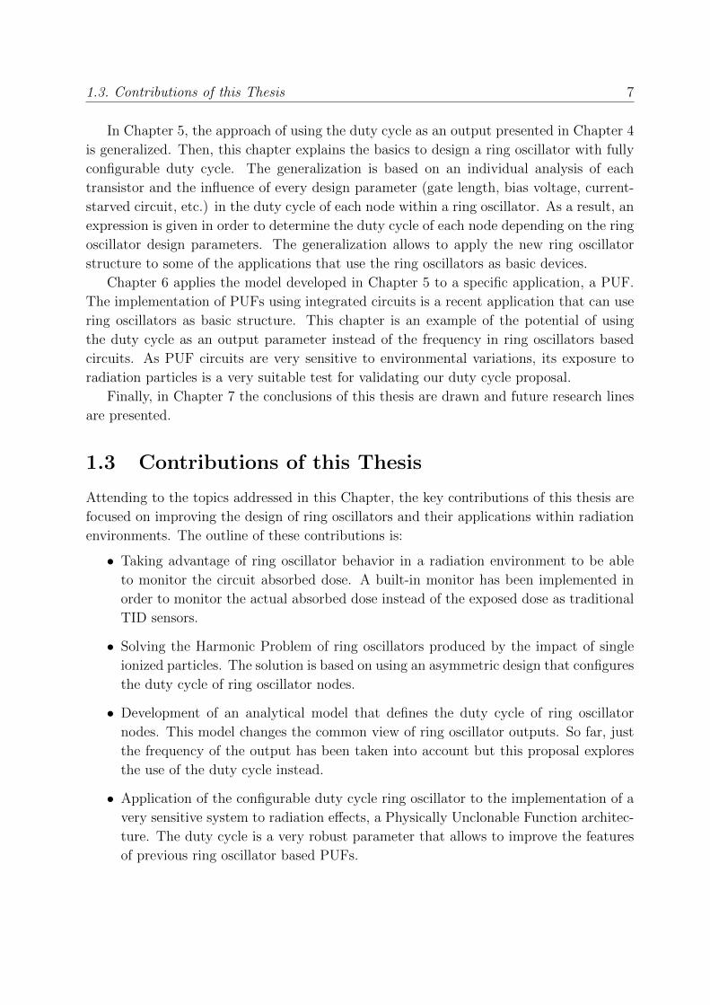
In Chapter 5, the approach of using the duty cycle as an output presented in Chapter 4
is generalized. Then, this chapter explains the basics to design a ring oscillator with fully
configurable duty cycle. The generalization is based on an individual analysis of each
transistor and the influence of every design parameter (gate length, bias voltage, current-
starved circuit, etc.) in the duty cycle of each node within a ring oscillator. As a result, an
expression is given in order to determine the duty cycle of each node depending on the ring
oscillator design parameters. The generalization allows to apply the new ring oscillator
structure to some of the applications that use the ring oscillators as basic devices.
Chapter 6 applies the model developed in Chapter 5 to a specific application, a PUF.
The implementation of PUFs using integrated circuits is a recent application that can use
ring oscillators as basic structure. This chapter is an example of the potential of using
the duty cycle as an output parameter instead of the frequency in ring oscillators based
circuits. As PUF circuits are very sensitive to environmental variations, its exposure to
radiation particles is a very suitable test for validating our duty cycle proposal.
Finally, in Chapter 7 the conclusions of this thesis are drawn and future research lines
are presented.
1.3 Contributions of this Thesis
Attending to the topics addressed in this Chapter, the key contributions of this thesis are
focused on improving the design of ring oscillators and their applications within radiation
environments. The outline of these contributions is:
• Taking advantage of ring oscillator behavior in a radiation environment to be able
to monitor the circuit absorbed dose. A built-in monitor has been implemented in
order to monitor the actual absorbed dose instead of the exposed dose as traditional
TID sensors.
• Solving the Harmonic Problem of ring oscillators produced by the impact of single
ionized particles. The solution is based on using an asymmetric design that configures
the duty cycle of ring oscillator nodes.
• Development of an analytical model that defines the duty cycle of ring oscillator
nodes. This model changes the common view of ring oscillator outputs. So far, just
the frequency of the output has been taken into account but this proposal explores
the use of the duty cycle instead.
• Application of the configurable duty cycle ring oscillator to the implementation of a
very sensitive system to radiation effects, a Physically Unclonable Function architec-
ture. The duty cycle is a very robust parameter that allows to improve the features
of previous ring oscillator based PUFs.

8 1. Introduction
1.4 Publications
The contributions previously outlined and the results of this thesis have been published in
the following international conferences and journals:
Papers in JCR indexed journals
• J. Agustin, C. Gil, M. Lopez-Vallejo and P. Ituero, ”Design and Characterization
of a Built-In CMOS TID Smart Sensor,” in IEEE Transactions on Nuclear Science,
vol. 62, no. 2, pp. 443-450, April 2015. doi: 10.1109/TNS.2015.2404532
• J. Agustin and M. Lopez-Vallejo, ”An In-Depth Analysis of Ring Oscillators: Ex-
ploiting Their Configurable Duty-Cycle,” in IEEE Transactions on Circuits and Sys-
tems I: Regular Papers, vol. 62, no. 10, pp. 2485-2494, Oct. 2015.
doi: 10.1109/TCSI.2015.2476300
• J. Agustin, M. L. Lopez-Vallejo, C. G. Soriano, P. Cholbi, L. W. Massengill and Y.
P. Chen, ”Efficient Mitigation of SET Induced Harmonic Errors in Ring Oscillators,”
in IEEE Transactions on Nuclear Science, vol. 62, no. 6, pp. 3049-3056, Dec. 2015.
doi: 10.1109/TNS.2015.2496169
International Conference Proceedings
• J. Agustin, C. G. Soriano, M. L. Vallejo and P. Ituero, ”A built-in CMOS Total
Ionization Dose smart sensor,” IEEE SENSORS 2014 Proceedings, Valencia, 2014,
pp. 70-73. doi: 10.1109/ICSENS.2014.6984935
• J. Agustin, M. L. Lopez-Vallejo, C. G. Soriano, P. Cholbi, L. W. Massengill and Y.
P. Chen, ”Efficient Mitigation of SET Induced Harmonic Errors in Ring Oscillators,”
in NSREC 2015, Boston, Jul. 2015.
• J. Agustin and M. L. Lopez-Vallejo, ”A temperature-independent PUF with a config-
urable duty cycle of CMOS ring oscillators,” 2016 IEEE International Symposium on
Circuits and Systems (ISCAS), Montreal, QC, 2016, pp. 2471-2474. doi: 10.1109/IS-
CAS.2016.7539093
Chapter 2
Foundations

Chapter 2
Foundations
2.1 Ring Oscillators
2.1.1 Theory of oscillators
Oscillators are the key block of many electronic systems. They are used to perform count-
less different operations such as clock for digital circuits, synchronization of communication
systems or radio frequency carrier generators. In general, an oscillator can be defined as
an autonomous circuit that converts DC power into a periodic waveform. There are many
types of oscillators, and many different circuit configurations that produce a variety of pe-
riodic waveforms. However, the most commonly used oscillations are reduced only to two
different types: the sinusoidal signal and the pulsed signal. Usually, sinusoidal oscillations
are used in analog designs while pulse oscillators are the basis of any digital system clock.
Despite the different fundamental mechanisms underneath each electronic oscillatory
behavior, the study of every oscillator is based on finding the startup conditions along with
the oscillation frequency as accurately as possible. Once these main characteristics have
been analyzed and validated, other figures of merit characterize the oscillators to allow their
comparison and classification. These features can be referred to physical characteristics
—resources, integrability, bias conditions— or to frequency performance —phase noise,
jitter or quality factor (Q)— depending on the requirements of the target application.
In order to analytically define the frequency of an oscillator, three different approaches
can be taken from the designer’s perspective [Rhe10]. The linear analysis is usually the
first step for oscillator design. While this type of analysis does not predict all oscillatory
characteristics, it establishes initial starting conditions and forms the foundation of the
design. The nonlinear analysis can predict the oscillator fundamental output level, the
harmonic content of the output spectrum or internal voltage and current waveform because
these issues are consequence of the nonlinearities of the used electronic components. Both
types of analysis characterize the oscillators at steady-state while transient techniques
consider the time-domain waveform of the oscillation specially at the beginning of the
oscillation. As for many applications the linear analysis is enough, this introduction is
focused on it, leaving the special considerations of each particular design to the advanced
analysis of nonlinear and transient techniques.
2.1. Ring Oscillators 11
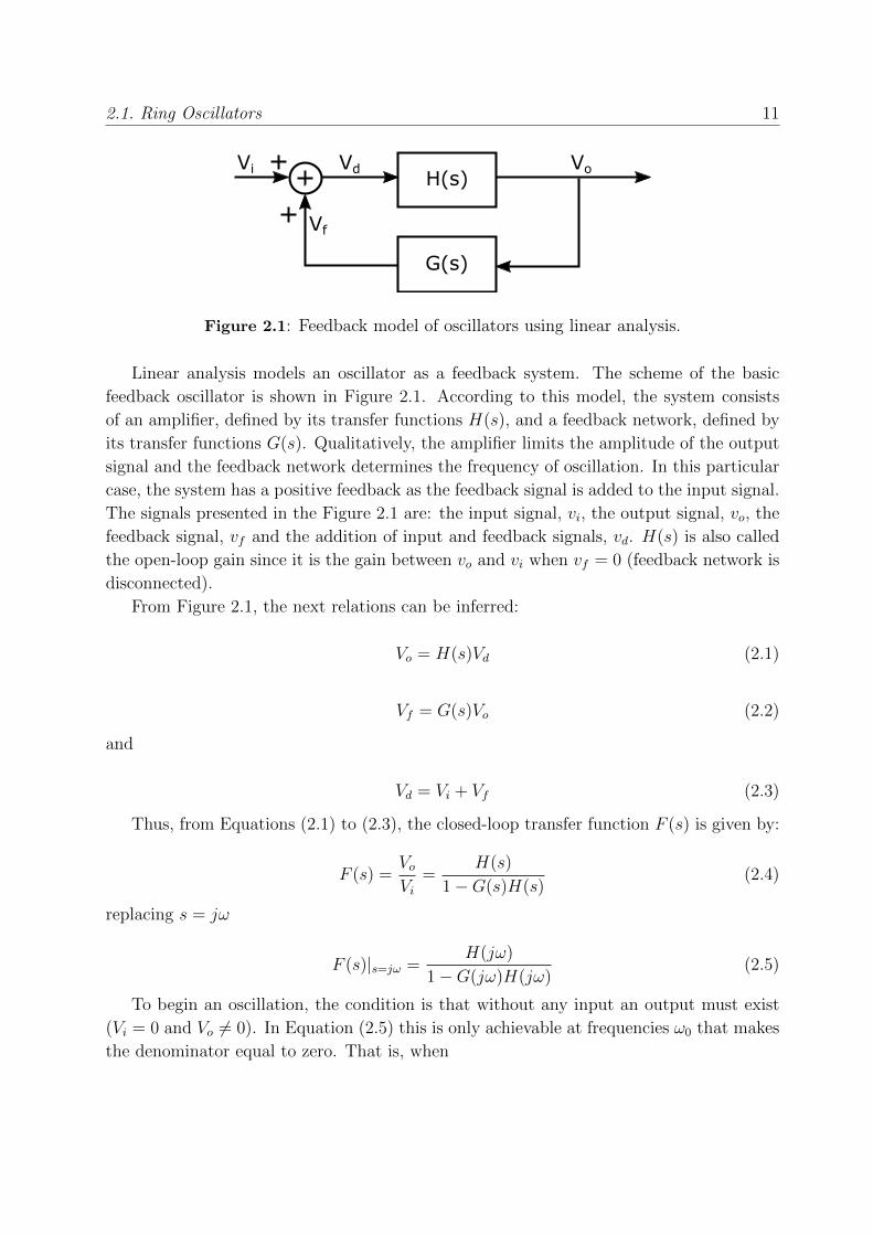
H(s)
G(s)
Vi Vd Vo
Vf
Figure 2.1: Feedback model of oscillators using linear analysis.
Linear analysis models an oscillator as a feedback system. The scheme of the basic
feedback oscillator is shown in Figure 2.1. According to this model, the system consists
of an amplifier, defined by its transfer functions H(s), and a feedback network, defined by
its transfer functions G(s). Qualitatively, the amplifier limits the amplitude of the output
signal and the feedback network determines the frequency of oscillation. In this particular
case, the system has a positive feedback as the feedback signal is added to the input signal.
The signals presented in the Figure 2.1 are: the input signal, vi, the output signal, vo, the
feedback signal, vf and the addition of input and feedback signals, vd. H(s) is also called
the open-loop gain since it is the gain between vo and vi when vf = 0 (feedback network is
disconnected).
From Figure 2.1, the next relations can be inferred:
Vo = H(s)Vd (2.1)
Vf = G(s)Vo (2.2)
and
Vd = Vi + Vf (2.3)
Thus, from Equations (2.1) to (2.3), the closed-loop transfer function F (s) is given by:
F (s) =VoVi
=H(s)
1−G(s)H(s)(2.4)
replacing s = jω
F (s)|s=jω =H(jω)
1−G(jω)H(jω)(2.5)
To begin an oscillation, the condition is that without any input an output must exist
(Vi = 0 and Vo 6= 0). In Equation (2.5) this is only achievable at frequencies ω0 that makes
the denominator equal to zero. That is, when
12 2. Foundations
1−G(jω0)H(jω0) = 0 (2.6)
or
G(jω0)H(jω0) = 1 (2.7)
This equation is known as the Barkhausen criterion and it establishes the initial con-
ditions of any oscillator. It is more often expressed in polar form as:
|G(jω0)H(jω0)| = 1 (2.8)
∠(G(jω0)H(jω0)) = ±n360◦ where n = 0, 1, 2, ... (2.9)
Equation (2.8) summarizes the fact that for oscillations to occur the loop gain must
be unity. And Equation (2.9) shows the need of the feedback signal, vf to be in phase
with the input signal, vi. If the model supposes a negative feedback network instead of the
positive one used in Figure 2.1, then this second condition is replaced by:
∠(G(jω0)H(jω0)) = ±n360◦ + 180◦ (2.10)
Previous equations analytically express how the oscillation begins without any input
excitation. The stability of the system is altered by the amplification of an electronic
noise. This noise, presented in every electronic circuit, is a white noise with a constant
Power Spectral Density (PSD). The feedback network filters the noise at the output. This
filtering makes that only the component w0 of the noise is added and amplified in the loop
what will generate the periodic output at the circuit fundamental frequency.
2.1.2 Types of oscillators
Oscillators can be classified depending on different features. We will divide them into two
groups according to the type of feedback network: resonant or non resonant oscillators.
Resonant oscillators use some kind of resonator to select or generate the oscillation
frequency. The resonator is a system that presents a peak in a parameter such as impedance
or vibration, at a fixed frequency which can be used to amplify this frequency component
and attenuate the rest. The most used resonant oscillators are:
• LC oscillators. In this type of oscillators, the feedback network is based on the
use of inductors and capacitors to form a tank circuit able to select a resonant
frequency. At this frequency, the equivalent impedance of the network is infinite.
The oscillation behavior comes from the conversion of electrostatic energy stored in
2.1. Ring Oscillators 13
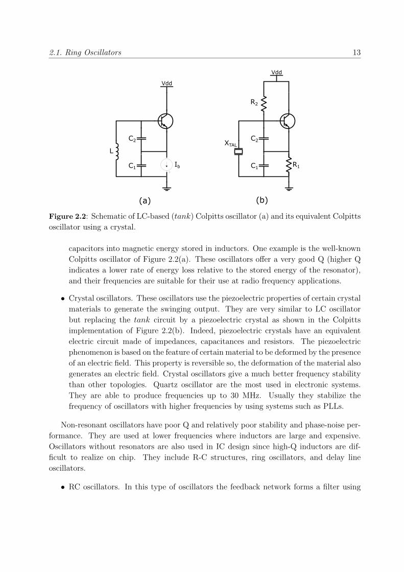
Vdd
C1
C2
R2
R1
XTAL
Ib
Vdd
C1
C2
L
(a) (b)
Figure 2.2: Schematic of LC-based (tank) Colpitts oscillator (a) and its equivalent Colpitts
oscillator using a crystal.
capacitors into magnetic energy stored in inductors. One example is the well-known
Colpitts oscillator of Figure 2.2(a). These oscillators offer a very good Q (higher Q
indicates a lower rate of energy loss relative to the stored energy of the resonator),
and their frequencies are suitable for their use at radio frequency applications.
• Crystal oscillators. These oscillators use the piezoelectric properties of certain crystal
materials to generate the swinging output. They are very similar to LC oscillator
but replacing the tank circuit by a piezoelectric crystal as shown in the Colpitts
implementation of Figure 2.2(b). Indeed, piezoelectric crystals have an equivalent
electric circuit made of impedances, capacitances and resistors. The piezoelectric
phenomenon is based on the feature of certain material to be deformed by the presence
of an electric field. This property is reversible so, the deformation of the material also
generates an electric field. Crystal oscillators give a much better frequency stability
than other topologies. Quartz oscillator are the most used in electronic systems.
They are able to produce frequencies up to 30 MHz. Usually they stabilize the
frequency of oscillators with higher frequencies by using systems such as PLLs.
Non-resonant oscillators have poor Q and relatively poor stability and phase-noise per-
formance. They are used at lower frequencies where inductors are large and expensive.
Oscillators without resonators are also used in IC design since high-Q inductors are dif-
ficult to realize on chip. They include R-C structures, ring oscillators, and delay line
oscillators.
• RC oscillators. In this type of oscillators the feedback network forms a filter using

14 2. Foundations
C3R3R2
R1
C2C1
Rf
R1
R2 R3
R4
C1
C2
(a) (b)
Figure 2.3: Schematic of a phase-shift RC oscillator (a) and a Wien oscillator (b).
Figure 2.4: 3-stage ring oscillator with inverter gates.
capacitors and resistors. They are used to generate lower frequencies. The most
common circuits are the phase shift and the Wien bridge oscillator. Their schematics
are shown in Figure 2.3.
• Ring oscillators and delay line oscillators. They are based on a closed loop of identical
elements. Each element delays the input signal and it also inverts it. The output
frequency depends on the number of stages and the delay of each one. They are
commonly used in IC circuits.
This thesis is focused on CMOS ring oscillators and their applications, with special
emphasis on radiation applications. Therefore, from this point we will only consider ring
oscillators for their study.
2.1.3 Ring Oscillators
A ring oscillator is a circuit made of a cascade of individual inverter stages in a feedback
configuration where the output signal oscillates with a period defined by the addition
of all stage delays. Usually, all the stages are identical, therefore the frequency is only
dependent on the stage delay and the number of stages. The simplest implementation is
the ring oscillator of Figure 2.4 which is made of three stages using inverter gates.

2.1. Ring Oscillators 15
Abidi declares in [A+06] that the ring oscillator is one of the most widely manufactured
integrated circuits of all. Foundries use ring oscillators on almost every semiconductor
wafer to monitor the gate delay and speed-power product of fabricated MOS inverters.
Automated measurements of oscillation frequency determine which wafers are acceptable,
and which fall outside an acceptable performance and must be discarded. Ring oscillators
have occupied this role since the earliest days of MOS IC technology because they are easy
to build, always oscillate, and are readily measured.
One of the reasons of the utilization of ring oscillators is their lack of capacitors, in-
ductors and resistors. The feasibility of these elements with practical values and quality
required the use of great area in modern integrated circuits against the high density achiev-
able with only transistors [Raz96]. Then designs with the absence of passive elements are
suitable for very compact oscillators.
2.1.4 Frequency of ring oscillators
As any oscillator, the main feature of a ring oscillator is its output frequency. Several
studies have tried to improve the accuracy of the ring oscillator model to calculate the
oscillation frequency. All of them have followed different approaches but starting from the
simplest equation for a ring oscillator with N stages:
f0 =1
2Ntd(2.11)
The understanding of this expression is straightforward. If a ring oscillator is made
of N equally designed stages and each stage has a time delay of td, then the total delay
of a period T is equal to twice the value of the propagation along the whole chain. The
accuracy of this expression is given by the precision of the calculation of td, the delay of
each gate. Therefore, many studies [DS03, SY08, MS10] have focused on finding the most
accurate value of this time through the analysis of every possible parameter that affects it.
These parameters depend on the type of the implemented stage: CMOS, BJT, differential,
etc. For example, Figure 2.5 shows the implementation of a ring oscillator with static
CMOS inverters where some of the most relevant parameters that define the frequency are
represented: W and L are the width and length of transistor channel, C is the capacitance
of a node and Vdd is the bias voltage.
Other studies [JSS10,RBH14] consider that Equation (2.11) is not accurate enough and
they propose to use linear analysis to determine the oscillation frequency. That way, the
oscillation frequency of a free running ring oscillator can be calculated by the application
of the linear analysis explained in Section 2.1.1. The first step is to define each of the
components of the linear model: the amplifier ant the feedback network.
To define the amplifier we will consider the example of the CMOS ring oscillator and
the characteristic of a CMOS inverter [RCN02]. The static CMOS normalized transfer

16 2. Foundations
Wp1Lp1
Wn1Ln1
Wp2Lp2
Wn2Ln2
Wp3Lp3
Wn3Ln3
Vdd1 Vdd2 Vdd3
C1 C2 C3
Figure 2.5: 3-stage ring oscillator with CMOS inverter gates.
Figure 2.6: Simulated Voltage Transfer Characteristic (a) and voltage gain (b) of CMOS
inverter [RCN02].
characteristic is plotted in the Figure 2.6 (a). This circuit is usually viewed from the point
of view of digital designers considering the operation of the device only in the region of
extreme nonlinearity where at the input logic ’0’ the inverter output is a logic ’1’ and
inversely with an input equal to ’1’ the output is ’0’. However, if the voltage gain of this
inverter (Figure 2.6 (b)) is also considered, there is a linear region where the static CMOS
inverter acts as an analog amplifier. This region is quite narrow and its characteristics are
not the best for an amplifier but they are enough to explain the start of the oscillation
fulfilling the Barkhausen criterion. In this case, the feedback network is modeled as a
system with a transfer function G(s) = 1.
Replacing the CMOS inverter by an equivalent amplifier with voltage gain A(s), the
linear analysis in the s-domain with the closed loop configuration is:
2.1. Ring Oscillators 17
C R
-gmC R
-gmC R
-gm
Figure 2.7: Model of ring oscillators for Linear Analysis.
H(s) = (A(s))N (2.12)
and consequently with the Barhausen criterion:
∠(A(jω0)) = θ = ±n360◦
Nand |(A(jω0)|N = 1 (2.13)
where θ represents the phase shift of each stage.
The linear model also considers the interconnection between the stages to calculate
the value of the gain. The interconnection can be modeled by RC elements as shown in
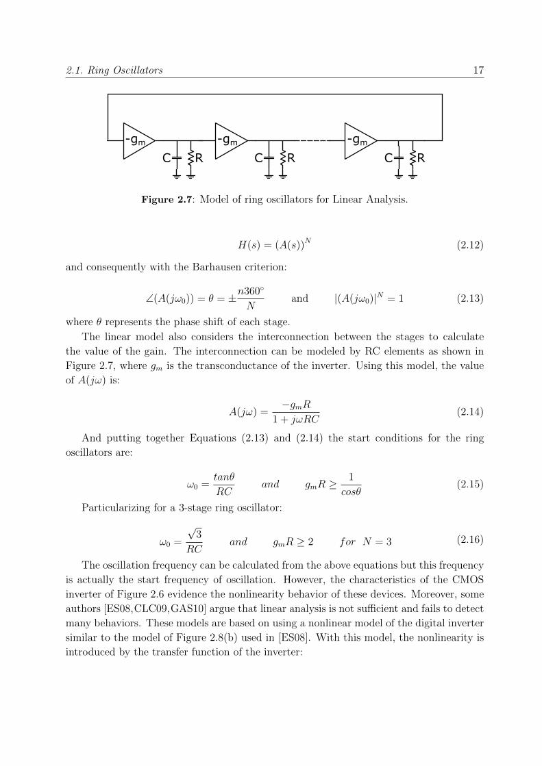
Figure 2.7, where gm is the transconductance of the inverter. Using this model, the value
of A(jω) is:
A(jω) =−gmR
1 + jωRC(2.14)
And putting together Equations (2.13) and (2.14) the start conditions for the ring
oscillators are:
ω0 =tanθ
RCand gmR ≥
1
cosθ(2.15)
Particularizing for a 3-stage ring oscillator:
ω0 =
√3
RCand gmR ≥ 2 for N = 3 (2.16)
The oscillation frequency can be calculated from the above equations but this frequency
is actually the start frequency of oscillation. However, the characteristics of the CMOS
inverter of Figure 2.6 evidence the nonlinearity behavior of these devices. Moreover, some
authors [ES08,CLC09,GAS10] argue that linear analysis is not sufficient and fails to detect
many behaviors. These models are based on using a nonlinear model of the digital inverter
similar to the model of Figure 2.8(b) used in [ES08]. With this model, the nonlinearity is
introduced by the transfer function of the inverter:

18 2. Foundations
Vi Vo
Cp
Vi VoVn-tanh(x) 1-Ts1+Ts
(a) (b)
Figure 2.8: (a) Digital inverter symbol with parasitic capacitor Cp and (b) proposed
nonlinear model [ES08].
Vn = −Vsattanh(Vi/Vs); (2.17)
where Vsat is the saturation voltage of the inverter and Vs adjusts the slope of the linear
region. The interconnection and parasitics are modeled by an all-pass filter with a transfer
function:
T (s) =1− Ts1 + Ts
(2.18)
where T = CP rout is the filter time constant and rout is the output resistance of the inverter.
The following differential equation models the complete behavior of the inverter:
Vo + T Vo = −Vsattanh(Vi/Vs) + TVsatVs
[1− tanh2(Vi/Vs)]Vi (2.19)
Defining x = Vi/Vref , y = Vo/Vref , α = Vref/Vs and β = Vsat/Vref that equation
transforms into:
y + y = −βtanh(αx) + α · β[1− tanh2(αx)]x (2.20)
where time is normalized with respect to T and Vref is an arbitrary reference voltage. And
α ·β defines the internal gain A of the inverting amplifier. Applying this model to a 3-stage
ring oscillator, the equations that define the behavior of each node (x,y,z) are:
x = −x− β tanh(αz) + αβz[1− tanh2(αz)]
y = −y − β tanh(αx) + αβx[1− tanh2(αx)]
z = −z − β tanh(αy) + αβy[1− tanh2(αy)]
(2.21)
The solution to these equation makes w0 = T/√
3 and > 1. Then while the oscillation
frequency can be equal in both models, the condition of the inverter gain is less restrictive
with the nonlinear analysis than with the linear model. Thus, the application of each
model depends on the accuracy and characteristics required in each application.

2.2. Radiation Effects in Electronics 19
All of these examples show how the efforts of previous studies have focused on deter-
mining, with high accuracy, the frequency of a ring oscillator due to being it considered
its most important feature. However, as we will see in this thesis: First, the simplest
approach using Equation 2.11 is enough for designing an application of ring oscillator as
a Total Ionization Dose Monitor. And second, previous studies have forgotten to explore
other features of ring oscillator such as the duty cycle. We will use the same Equation 2.11
to derive a model of duty cycle in ring oscillators. And we will use that model to implement
improved ring oscillator based applications.
2.2 Radiation Effects in Electronics
The Introduction of this thesis has summarized the most important facts and research
topics of radiation effects in electronics along the last decades. Those topics and the
relevant concepts needed to understand this thesis are introduced in this section. First,
the typical units used to refer the physical magnitudes of radiation effects are outlined.
Then, the different environments able to produce radiation effects in electronic systems
are characterized. Those radiation effects are classified and briefly described together with
some of the mitigation techniques used to overcome their impact. Finally, the potential
hazards of ring oscillators working within radiation environments are explained.
2.2.1 Radiation Units
The next definitions and units characterize the physical interactions of materials with
radiation particles.
Rad and Gy
The rad and gray (Gy) are the units of absorbed radiation dose. Even though the gray is
the International System (SI) unit, the rad is used for most published works by academia
and industry community in radiation effects. The absorbed dose is defined as the amount
of energy deposited in a material, so one rad corresponds to 100 ergs of energy deposited
in one gram of material. As absorption depends on the target material, the radiation dose
is indicated with the target material, for example, 100 rad(SiO2). One Gy corresponds to
a deposition of 1 joule per kg of target material. Then, one rad corresponds to 10−2 Gy
(1 rad = 1 cGy).
Linear Energy Transfer
The interaction of a particle passing through matter results in the transfer of its energy to
the material. This interaction is measured by the linear rate of energy loss and it is called

20 2. Foundations
Linear Energy Transfer (LET). Therefore, LET is dependent on the target material and
on its density. Usually, the LET use values normalized to a unit density for each material.
The result is an energy loss per unit length, dE/dx (MeV/cm), divided by the material
density, ρ (mg/cm3)
LET =1
ρ· dEdx
(MeV · cm2/mg) (2.22)
Cross Section
The cross section, σ, is defined by the ratio of the number of single events observed on the
device by the particle fluency (particles per cm2) received by the component. Therefore, σ
is a measure of the sensitivity of a device. The cross section can also be interpreted as the
probability that a particle impact provokes a single event in the hit node. The equation
used to calculate the cross section is:
σ =# of observed events
fluency(2.23)
2.2.2 Environments
The design of electronic circuits for radiation applications is highly dependent on the
environment they will be exposed. In order to have reliable, cost-effective designs and
implement new devices, the nature of the environment must be understood. Underes-
timating the radiation levels leads to excessive risk and can result in degraded system
performance. Overestimating the radiation levels can lead to excessive shielding, reduced
payloads, over-design and increased cost [XOO12]. We divide the environments into two
different categories: space, which has been extensively characterized in terms of radiation
since the first explorations, and terrestrial, where radiation has become a problem in the
last years due to the shrinking of the technology.
Space Environment
Before the space era the only manifestations of the presence of radiations in space were
the deformation of the ionized tail of comets caused by the solar wind, the aurora borealis
whose origin was not well understood and the ionization of air produced by cosmic radia-
tion [BX08]. Since the first space missions, it was evident that the space environment is a
highly disruptive medium for electronic devices. Beyond the natural protection provided
by a planet’s atmosphere, various types of radiation can be encountered. Figure 2.9 shows
an interpretation of the different environments found in space due to the interaction of par-
ticles generated at the Sun and the planets’ magnetosphere. These particles are generally
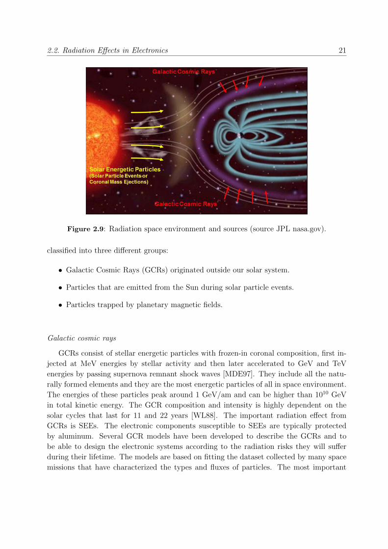
2.2. Radiation Effects in Electronics 21
Figure 2.9: Radiation space environment and sources (source JPL nasa.gov).
classified into three different groups:
• Galactic Cosmic Rays (GCRs) originated outside our solar system.
• Particles that are emitted from the Sun during solar particle events.
• Particles trapped by planetary magnetic fields.
Galactic cosmic rays
GCRs consist of stellar energetic particles with frozen-in coronal composition, first in-
jected at MeV energies by stellar activity and then later accelerated to GeV and TeV
energies by passing supernova remnant shock waves [MDE97]. They include all the natu-
rally formed elements and they are the most energetic particles of all in space environment.
The energies of these particles peak around 1 GeV/am and can be higher than 1010 GeV
in total kinetic energy. The GCR composition and intensity is highly dependent on the
solar cycles that last for 11 and 22 years [WL88]. The important radiation effect from
GCRs is SEEs. The electronic components susceptible to SEEs are typically protected
by aluminum. Several GCR models have been developed to describe the GCRs and to
be able to design the electronic systems according to the radiation risks they will suffer
during their lifetime. The models are based on fitting the dataset collected by many space
missions that have characterized the types and fluxes of particles. The most important
22 2. Foundations
models are the Badhwar-O’Neill Model [GOS15], the Buchvarova-Velinov Model [BD13],
the CHIME Model [CCC+94] and the Nymmik Model [Nym06]. All these models were eval-
uated against an extensive database of published measurements of elemental differential
energy spectra spanning the time period from 1954 to the present. The most recent version
of Nymmik Model was selected as the international standard model (ISO 15390:2004).
Particles generated during solar particle events
The Sun generates a huge amount of particles through many kinds of eruptions. Among
them, the most important and relevant for the study of their impact in electronics are
the solar flares and the Coronal Mass Ejections (CME). They are deeply described in
[MSHL01, ADK99]. Both involve gigantic explosions of energy, but are essentially quite
different. They may occur at the same time — the strongest flares are almost always
correlated with coronal mass ejections — but they generate different emissions, they look
and travel differently, and they have different effects.
Solar flares result when the localized energy storage in the coronal magnetic field be-
comes too large and causes a burst of energy to be released. Flares can last minutes to
hours. Traveling at the speed of light, it takes eight minutes for the light from a solar flare
to reach Earth. Some of the energy released in the flare also accelerates very high energy
particles that can reach Earth in tens of minutes. They tend to be electron rich, and have
high 3He content relative to 4He.
A CME, on the other hand, is a large eruption that hurls solar matter into space (a gas of
free ions and electrons) that drives a shock wave outward and accelerates particles.Traveling
over a million miles per hour, the plasma takes up to three days to reach Earth. CMEs
are proton rich and have small 3He content relative to 4He.
It is critical to define the content and energy distribution of solar particle events for
bounding the performance of advanced electronics within radiation environments, however
it is a really difficult task. To overcome this challenge, several solar particle event models
have been created [FSWG93,XBS+99,XSB+00,ADK99].
Particles trapped inside Earth’s magnetosphere
The magnetosphere is formed by the interaction of the solar wind with Earth’s magnetic
field. This dipole field traps protons and electrons within two magnetic field lines called the
Van Allen Belts. Since its discovery in 1959 [VAF59a,VAF59b], these radiation belts have
been the topic of many studies and an important problem for electronic devices passing
through these areas. Trapped protons have energies up to hundreds of MeV with fluxes up
to 105 cm−2·s−1 for energies >10 MeV.

2.2. Radiation Effects in Electronics 23
Figure 2.10: Sketch of the Van Allen belts as a result of solar particles interaction with
Earth’s magnetosphere (source JPL nasa.gov).
It is specially important the fact that the rotational and magnetic axes are misaligned
by approximately 11◦ what creates a particular zone called South Atlantic Anomaly (SAA).
Because of that tilt and their center displacement, part of the inner edge of the trapped
proton belts is at a much lower altitude off the southeast coast of Brazil. The SAA and
the Van Allen belts are shown graphically in Figure 2.10.
The composition and dynamics of particles within radiation belts continue being a
hot topic nowadays and recently, a pair of probes [SRB+13] were sent to explore the
characteristics of the radiation belt on Earth’s magnetosphere. There are also various
Earth-based trapped proton models available, including AP-9, CRRESPRO or AE9 whose
data have been reviewed in [JOH+15].
The cosmic particles are not only trapped in Earth, it is a phenomenon typical of
every magnetized planet. The five strongly magnetized planets in the solar system, Earth,
Jupiter, Saturn, Uranus, and Neptune have their own magnetosphere with many similarities
and specificities. They have robust electron radiation belts [MF10].
Terrestrial Environment
At terrestrial level there are mainly two types of particles that contribute to the generation
of a radiation environment able to interact with the structure of semiconductor electronic
devices. They are the neutrons, generated by cosmic interaction with atmosphere, and the
alpha particles, resulted from the natural decay of radioactive materials [RG05].

24 2. Foundations
Figure 2.11: Cascade interactions of cosmic particles with the atoms of the atmosphere.
High-Energy Neutrons
As cosmic ray and solar particles enter the top of the Earth’s atmosphere, they are
attenuated by interaction with the nitrogen and oxygen atoms that conforms the majority
of atoms of the atmosphere. The result is a production of complex cascades of secondary
particles through nuclear reactions with the nitrogen and oxygen nuclei. These secondary
particles continue interacting with the atoms of the atmosphere creating tertiary particle
cascades and so on (as shown in Figure 2.11). At terrestrial altitudes, less than 1% of the
primary flux reaches sea-level where the particle flux is composed predominantly of elec-
trons, muons, neutrons, and a smaller fraction of protons. Due to the relatively high LET
of the resulting secondary particles from neutron reactions and their abundance as com-
pared with most of the other particle types, neutrons are considered the dominant source
in terms of radiation effect in electronics [HS00]. Nevertheless the extremely shrinking
of technology allows the appearance of single effects as a result of interaction with other
particles such as muons [SRM+11].
There are three primary factors that modify the neutron flux at a particular terrestrial
location and time. The dominant factor is altitude, the neutron flux varies about twenty
times from sea-level to high altitudes (around 3000 m). The second factor that modulates
the neutron flux is the latitude, at sea level, the neutron flux is twice at equatorial latitude
that at polar latitudes. The solar activity cycle also defines the neutron flux of terrestrial
environment. This cycle lasts about eleven years and its effects can modify the neutron
flux from the minimum to the peak in three times, although solar flares and CMEs activity
could also generate sudden and intense changes in the neutron flux [KPnS15].

2.2. Radiation Effects in Electronics 25
Alpha Particles
The alpha particles are emitted from the disintegration of unstable isotopes. They
are composed of helium atoms with two protons. This process is a natural behavior of
this kind of isotopes and it does not need any external interaction or energy. When an
alpha particle travels through a material, it loses its kinetic energy predominantly through
interactions with the bound electrons of that material and thus leaves a trail of ionization
in its wake. The higher the energy of the alpha particle, the farther it travels before
being absorbed by the material. The importance of alpha particles is because the ceramic
packages used in the fabrication processes of electronic devices are able to emit this kind
of particles [SMT94]. Alpha particles are easily stopped by device packaging materials as
their range is of few tenths of microns. Thus, alpha emission outside of the device does
not need to be considered. Only alpha emission internal to the device can interact with
circuits and cause a soft error event.
The impact of alpha particles radiation in electronic devices plays an important role
especially for accelerated radiation test. As will be explained in Chapter 4, this kind of
radiation is very common for testing circuits reliability against SEEs.
2.2.3 Radiation Effects
The interaction of the energetic particles introduced in the previous section with the mate-
rials used for the fabrication of electronic devices causes different types of radiation effects.
These effects have been deeply studied for almost every material, fabrication process and
technology node developed for semiconductor electronics. As a summary of those studies,
the effects are the consequence of the energy deposition as a result of the interactions with
the energetic particles. The energy is deposited by the passage of those particles through
materials, either through direct or indirect processes. In semiconductor materials, that en-
ergy is converted into electron-hole pairs and atomic dislocations. They are usually divided
into two different categories: cumulative effects or SEEs.
Cumulative Effects
Cumulative effects refer to the effects that are the result of long term exposition to radiation
environments. Depending on the characteristics of the exposed particles, the cumulative
effects can vary just the charge distribution within the device structure what is called
TID or they can physically affect the atomic structure of the material what is referred as
Displacement Damage Effect (DDE).
Total Ionization Dose
26 2. Foundations
TID has been the most studied phenomenon of radiation effects in electronic devices.
This is because the degradation could be evaluated at the end of the application lifetime
without the need of continuously monitoring the system expecting for an error.
The electron-hole pairs generated by the interaction of ionized particles with semi-
conductor materials leads to a progressive degradation of devices. For example, in MOS
transistors, the new generated carriers produce a redistribution of charges in the structure
as a consequence of the trapping of the carriers in the interfaces and gate oxides provoking
the alteration of threshold voltages. The effect of TID is accumulative but, at the same
time, it is generally reversible through the application of annealing techniques what allows
the partial recovering of the degradation by thermal processes.
Displacement Damage Effects
DDE refers to the dislodging of atoms from their normal lattice sites in a target ma-
terial by impinging energetic radiation. The resulting damage causes degradation of the
electronic and optical properties of materials and devices. That degradation is generally
due to the introduction of new energy levels in the semiconductor bandgap, which changes
properties such as recombination lifetime [SP13]. Displacement damage produces perma-
nent changes in material and device properties, although thermal and injection annealing
can alter the observed effects.
In general, minority-carrier devices are relatively sensitive and majority-carrier devices
are relatively insensitive. For example, MOS devices generally are radiation-tolerant in
terms of displacement damage effects. Although at sufficiently high particle fluences, all
devices will eventually degrade due to displacement damage effects [SMM03].
Single Event Effects
Opposite to the long term effects that cause the progressive degradation of the electronic
devices, the SEEs denote all of the phenomena created by the impact of an individual
energetic particle through the semiconductor or insulator materials used in the fabrications
of integrated circuits [Nar08]. There are several mechanisms encompassed within the SEE
term. The following is a brief list and description of each type:
• Single Event Transient (SET). A SET induces a pulse generated at the hit node and
that propagates along the circuit. The pulse dynamics are determined by both process
and circuit parameters. Whenever the charged particle passes through a depletion
region a transient is created. Whether or not this transient results in an error depends
on a number of factors, including the final pulse width, pulse amplitude and circuit
dynamics [BEM+06]. SETs are a major concern for combinational circuits.
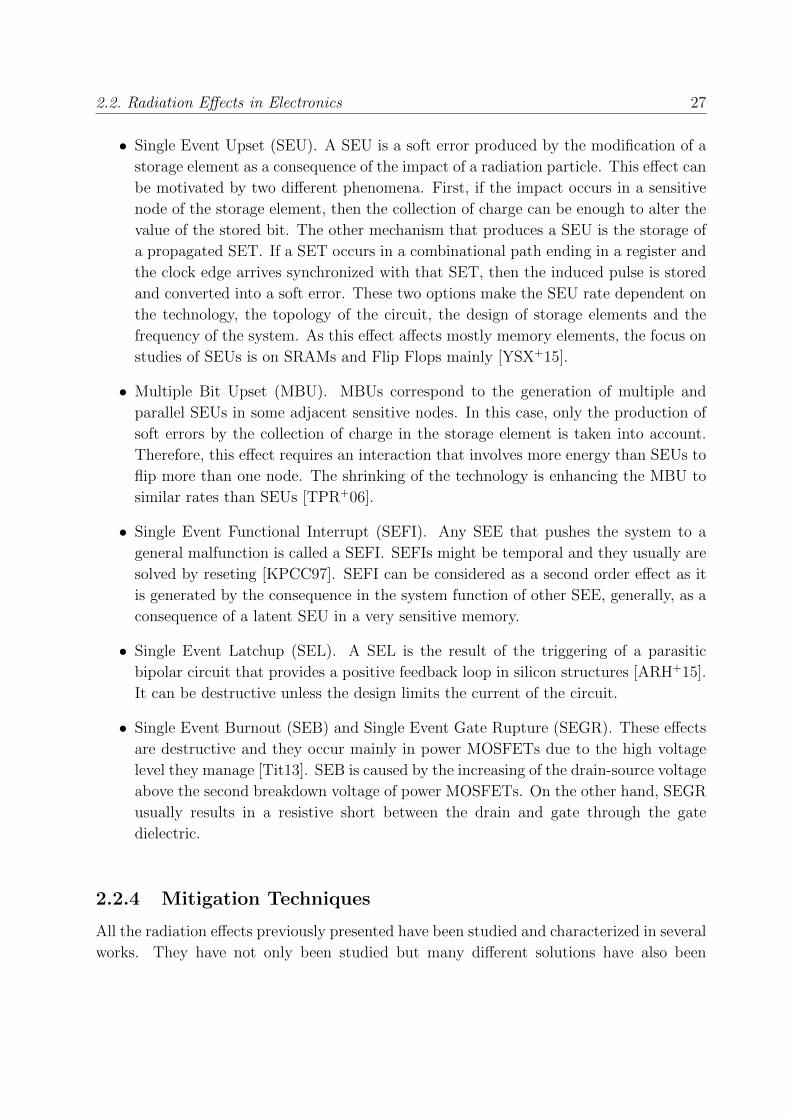
2.2. Radiation Effects in Electronics 27
• Single Event Upset (SEU). A SEU is a soft error produced by the modification of a
storage element as a consequence of the impact of a radiation particle. This effect can
be motivated by two different phenomena. First, if the impact occurs in a sensitive
node of the storage element, then the collection of charge can be enough to alter the
value of the stored bit. The other mechanism that produces a SEU is the storage of
a propagated SET. If a SET occurs in a combinational path ending in a register and
the clock edge arrives synchronized with that SET, then the induced pulse is stored
and converted into a soft error. These two options make the SEU rate dependent on
the technology, the topology of the circuit, the design of storage elements and the
frequency of the system. As this effect affects mostly memory elements, the focus on
studies of SEUs is on SRAMs and Flip Flops mainly [YSX+15].
• Multiple Bit Upset (MBU). MBUs correspond to the generation of multiple and
parallel SEUs in some adjacent sensitive nodes. In this case, only the production of
soft errors by the collection of charge in the storage element is taken into account.
Therefore, this effect requires an interaction that involves more energy than SEUs to
flip more than one node. The shrinking of the technology is enhancing the MBU to
similar rates than SEUs [TPR+06].
• Single Event Functional Interrupt (SEFI). Any SEE that pushes the system to a
general malfunction is called a SEFI. SEFIs might be temporal and they usually are
solved by reseting [KPCC97]. SEFI can be considered as a second order effect as it
is generated by the consequence in the system function of other SEE, generally, as a
consequence of a latent SEU in a very sensitive memory.
• Single Event Latchup (SEL). A SEL is the result of the triggering of a parasitic
bipolar circuit that provides a positive feedback loop in silicon structures [ARH+15].
It can be destructive unless the design limits the current of the circuit.
• Single Event Burnout (SEB) and Single Event Gate Rupture (SEGR). These effects
are destructive and they occur mainly in power MOSFETs due to the high voltage
level they manage [Tit13]. SEB is caused by the increasing of the drain-source voltage
above the second breakdown voltage of power MOSFETs. On the other hand, SEGR
usually results in a resistive short between the drain and gate through the gate
dielectric.
2.2.4 Mitigation Techniques
All the radiation effects previously presented have been studied and characterized in several
works. They have not only been studied but many different solutions have also been
28 2. Foundations
RadiationEffects
SinglehEventEffectsh(SEEs)
CumulativehEffects
TotalhIonizationDoseh(TID)
DisplacementhDamageEffectsh(DDE)
Destructive Non-destructive
SinglehEventLatchup(SEL)
SinglehEventGatehRuptureh(SEGR)
SinglehEventBurnouth(SEB)
SinglehEventUpseth(SEU)
MultiplehBitUpseth(MBU)
SinglehEventTransienth(SET)
SinglehEventhFunctionalhInterrupth(SEFI)
Figure 2.12: Classification of Radiation Effects in Electronics.
proposed to remove or mitigate the negative effects they produce in electronic system
performance. The mitigation techniques proposed are very diverse and they use different
approaches to solve the problems. The selection of a particular methodology depends on
the particular constraints of each application such as: environment, resources, cost, etc. In
this section the most relevant methods to overcome the radiation effects are summarized
and categorized.
Shielding
The first approach to mitigate the effects of radiation is the use of shielding. This method
tries to reduce the flux of particles that reach the electronic circuits by using dummy ma-
terials to trap the environment particles. These materials are specially selected for their
absorption of radiation particles due to their atomic structure together with other require-
ments of the particular application such as thermal resistances, lightweight or mechanical
features.
In some cases the shielding is intrinsically implemented by the structure of the space-
craft in space applications. In other cases, the location of circuits inside the system package
must be taken into account to minimize the radiation particles in sensitive circuits. Shield-
ing is predominately used to mitigate TID [ZMG12] but it is also used to protect against
single events even though it is not as effective [PXS+10].

2.2. Radiation Effects in Electronics 29
Radiation Hardened By Process
Radiation Hardening By Process (RHBP) is a term that describes a method to harden a
device to radiation effects using the fabrication process. Opposite to the shielding where
the design or the fabrication process of electronic components are unaltered, the RHBP is
based on carefully selecting the bulk material or by modifying the process and the design
of device layers used to create a semiconductor device.
One of the most extended technology used for RHBP is the Silicon on Insulator (SOI)
[RZB+12,PAH14]. SOI technologies are designed to be relatively immune to TID and they
have also shown some immunity to SEEs [dSFdSR+13]. SOI MOSFETs are more tolerant
to single event, thanks to the buried oxide layer, that isolates the active silicon region
from the substrate, in comparison to transistors implemented with CMOS conventional
bulk technology [GRP+13,RAGM]. Some of the III-V materials such as Gallium Arsenide
(GaAs) [NZS+15] and Silicon Germanium (SiGe) [Cre13] have shown resistance to radiation
effects. Modern technologies such as FinFETs have also proved being a good alternative
to bulk technologies for radiation sensitive applications [HAR15].
The benefit of the RHBP technique is the enhanced hardness without changing any
design. While the main drawback of the RHBP technique is the additional process steps
required during fabrication or the use of a niche technology. Both approaches increase the
cost of fabrication exponentially.
Radiation Hardened By Design
Another approach to mitigate the radiation effects in electronic systems relies on standard
commercial technologies to achieve the hardening by design techniques. This method is
called Radiation Hardening By Design (RHBD). As the design of a system is divided
into different levels of abstraction, the application of RHBD strategies is also implemented
at each different level, from the basic structure level to the system level. These types of
techniques have been the goal of most of the studies due to the drastic reduction of costs
compared to the use of special RHBP technologies [GMW08, CLS15]. However, in many
applications it is not possible to fulfill the requirements by using only RHBD techniques
and they are used together with RHBP technologies or shielding designs. Next, we outline
some of the most used RHBD methodologies divided according to the three different design
levels of abstraction: layout, circuit and system.
Layout
The design modifications that are implemented in the layout level are mainly focused
on two aspects, transistor sizing and charge-collection avoidance. At this level TID and
SEEs mitigation techniques are feasible in contrast to the circuit and system perspective.
30 2. Foundations
Increasing the overall transistor size improves the transistor performance against radi-
ation effects [ZM04,ZM06]. Instead of just increasing the transistor size, other approaches
have also proposed the use of different transistor structures [SGA02,XlS14]. It is important
not only the size of the transistor but its location with respect to other sensitive nodes as
is shown in [BSA+05]. However, the system tends to operate slower due to the increased
capacitance of larger devices. While RHBD increases the transistor size, it maintains ad-
herence to the process design rules. This allows RHBD to be implemented on any process
without requiring waivers or process modifications. Implementing RHBD is just a matter
of creating a new library and then synthesizing the design using that library.
Apart from using different transistor layouts, the rest of layout mitigation techniques
tries to avoid the charge collection of radiation induced carriers. This goal is achieved by
using special structures such as guard rings or dummy contacts to favor the path of those
charges through these structures instead of through device interfaces [BSA+05].
Circuit
As mentioned above, working at circuit level is suitable for solving SEEs while cumu-
lative effects are out of the scope from this level of abstraction. Circuit techniques are
based on redesigning the most basic gates or devices to tolerate the induced effects of a
single event. At this level, flip flops have occupied most efforts to design radiation tolerant
circuits. This is a direct consequence of the vulnerability of these devices to SEUs together
with their relevancy in every sequential design. To assure the hardening of circuits, every
method at circuit level is based on redundancy. Redundancy can be used to mitigate SEE
as is shown in the three next implementations of radiation hardened flip flops [LCS+16].
• Triple Modular Redundancy
Triple Modular Redundancy (TMR) is a very used structure to mitigate the effect
of SEUs or SETs [PK15, CBDN14, MKY+13]. Figure 2.13 shows the basic TMR
scheme. Using three identical flip flops with a single input, the three outputs are
voted on by a majority voter circuit. The voter drives the output with the signal
identical at least in two of its inputs. TMR is used because it is very unlikely that
more than one circuit would be affected by an upset or transient at a given time.
To avoid that special case, the three modules are usually physically separated using
layout mitigation techniques so that in new technologies there is not a multiple-node
hit creating two simultaneous upsets. In this type of circuits, the voter is the most
sensitive part, so it requires special treatment [DGA14].
• Temporal Latch
The TMR flip flop is hardened to SETs if the particle hits only the input of one the
replicated flip flops. However, if the particle impacts in the common input, it could
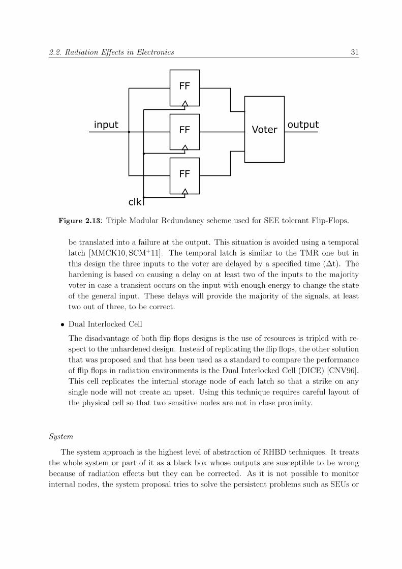
2.2. Radiation Effects in Electronics 31
FF
FF
FF
input
clk
Voter output
Figure 2.13: Triple Modular Redundancy scheme used for SEE tolerant Flip-Flops.
be translated into a failure at the output. This situation is avoided using a temporal
latch [MMCK10, SCM+11]. The temporal latch is similar to the TMR one but in
this design the three inputs to the voter are delayed by a specified time (∆t). The
hardening is based on causing a delay on at least two of the inputs to the majority
voter in case a transient occurs on the input with enough energy to change the state
of the general input. These delays will provide the majority of the signals, at least
two out of three, to be correct.
• Dual Interlocked Cell
The disadvantage of both flip flops designs is the use of resources is tripled with re-
spect to the unhardened design. Instead of replicating the flip flops, the other solution
that was proposed and that has been used as a standard to compare the performance
of flip flops in radiation environments is the Dual Interlocked Cell (DICE) [CNV96].
This cell replicates the internal storage node of each latch so that a strike on any
single node will not create an upset. Using this technique requires careful layout of
the physical cell so that two sensitive nodes are not in close proximity.
System
The system approach is the highest level of abstraction of RHBD techniques. It treats
the whole system or part of it as a black box whose outputs are susceptible to be wrong
because of radiation effects but they can be corrected. As it is not possible to monitor
internal nodes, the system proposal tries to solve the persistent problems such as SEUs or

32 2. Foundations
MBUs and their potential consequences such as SEFIs without dealing with internal SETs.
Three of the most used techniques are:
• TMR and Time-Triple Modular Redundancy
TMR is also applicable at system level as it is at circuit level. The general scheme is
the same for all types of TMR, three items followed by a voter. In this case it is done
at the component level. For example, the component can be a processor [GOB13] or
an FPGA [HALV11] or a simple circuit that performs a particular task [SCEGV15].
Then, the TMR would be done using three processor chips or three FPGAs or three
identical implementations of the circuit and a voter. Given the complexities of a
bigger system, the voter would need to be nearly as complex. Hence, the application
of TMR at this level includes complexity in communication and synchronization.
Time-Triple Modular Redundancy (TTMR) is used in a processor application and
involves the use of hardware and software to combat errors [CM03]. TTMR combines
time and spatial redundancy within a Very Long Instruction Word microprocessor
or DSP to achieve its unique SEU mitigation capabilities.
• Scrubbing
Scrubbing is quite frequently performed on memories and SRAM based FPGAs
[WH16, HALV13]. SEUs and MBUs in the configuration memory of SRAM based
FPGAs can be mitigated by writing a known and correct bitstream to the corruptible
device. This technique is often referred to as scrubbing and several types of implemen-
tations can be found [SVIE15]: blind/readback, device/frame-oriented, periodic/on-
demand or external/internal. The differences between the different implementations
are how and when the configuration memory of this devices is read. The two critical
points of scrubbing are that the correct bitstream called “golden” needs to be a fully
reliable memory and the availability of the system during writing stage depends on
the critically of the system.
• Error Detection And Correction
Error Detection And Correction (EDAC) is used to detect errors and allow them to
be corrected [CCTM16]. There are many types of EDAC from simple single parity
bit schemes to multiple bit coding schemes. Depending on the type of EDAC used,
it can detect and correct single or multiple bit errors. EDAC schemes use extra bits
to store information necessary to recreate the correct bit.
Figure 2.14 classifies the different strategies presented to design reliable applications
within radiation environments. As every design requires different radiation tolerance, the

2.2. Radiation Effects in Electronics 33
Radiation EffectsMitigation Strategies
Layout Circuit
TransistorSizing
Enclose LayoutTransistors (ELT)
Guard Rings
Triple ModularRedundancy (TMR)
Temporal Latches
Dual InterlockedCell (DICE)
Radiation Hardeningby Design (RHBD)
Radiation Hardeningby Process (RHBP)
Shielding
System
Triple ModularRedundancy (TMR)
Scrubbing
Error DetectionAnd Correction (EDAC)
Figure 2.14: Classification of Radiation Effects mitigation strategies.
type of mitigation technique to be implemented will hardly depend on each particular
application.
Attending to the mentioned mitigation techniques, the industry of semiconductors for
radiation environments has utilized mainly three different types of technology to implement
systems suitable for operating in those especially hostile conditions. The first approach
is the use of technologies that are inherently hardened against radiation effects. They
implement some RHBP techniques that assure a high tolerance. The second approach
uses RHBD techniques in commercial technologies to generate a system that is tolerant
to radiation effects. And the third methodology is based on using Commercial Off-The-
Self (COTS) components. COTS term refers to any electronic device that does not have
guaranteed radiation tolerance or hardened performance. Therefore, the last option relies
on unhardened components to implement systems for radiation environments but taking a
high risk of malfunctions. Table 2.1 summarizes the main advantages and disadvantages
of each technology approach.
In terms of radiation hardness, the RHBP technologies outperform both RHBD designs
and COTS based systems. As the technology in inherently hardened, the level of toler-
ance is defined by the fabrication process, what assures the robustness against radiation
effects. At the same time, these technologies are much more expensive as a consequence
of their special processes. The small number of applications that require these particular
technologies makes them very expensive because of the non-recurrent costs, low yield and
small number of fabricated batches.
On the other hand, the tolerant systems that implement RHBD designs in commercial
technologies increase the fabrication cost with respect to unhardened systems just because
they usually spend more resources but they do not need a special fabrication process.

34 2. Foundations
Table 2.1: Comparison of the different technologies implemented for radiation systems.
Hardness Cost Design Test Performance
RHBP Technologies ⇑⇑⇑ ⇑⇑⇑ ⇓ ⇓ ⇓RHBD Designs ⇑⇑ ⇑ ⇑⇑ ⇑ ⇓
COTS ⇓ ⇓ ⇓ ⇑⇑ ⇑⇑
However, the RHBD approach requires more design time than the other approaches. As
was presented, the implementation of radiation tolerant systems with RHBD techniques is
mainly based on redundancy at different levels of abstraction. Therefore, the design effort
is higher than the implementation of designs with tolerant technologies or COTS.
Another important aspect in radiation hardened design is the cost of radiation tests.
Regarding this topic, tolerant technologies are the less restrictive because the foundry has
already performed all the tests that characterize and assure the level of hardness. RHBD
designs require a more complete test campaign but COTS based systems need a very
exhaustive test campaign to limit the risks in real operation.
Finally, in terms of device performance, COTS systems are the best option as they
can be implemented with the last technology available in the market while the other two
approaches are usually implemented with mature technology nodes that imply worst per-
formance in frequency, power consumption, etc.
Putting all together, radiation hardened systems usually implement hybrid solutions to
exploit the benefit of each different approach. In this Thesis, as the goal is the improvement
of ring oscillators in radiation environments first and then in traditional applications, we
will focus on the implementation of ring oscillators in commercial technologies using RHBD
techniques to improve the radiation hardening.
2.3 Ring oscillators in radiation environments
As the objective of this thesis is the implementation of ring oscillator based applications
for radiation environments, in this section the impact of all previous introduced effects and
the proposed applications in previous studies are presented.
Total Ionization Dose
As mentioned in Section 2.1, ring oscillators are integrated in all fabrication processes
to monitor the performance and variations of each batch. The same features that make
these devices suitable for this task at ground level are exploited for characterizing the
different technologies at different radiation environments. In [OLMY98] the same ring

2.3. Ring oscillators in radiation environments 35
oscillator test vehicle design is used to compare the hardness of four different fabrication
process from three different foundries. And every technology characterization uses ring
oscillators [BVA+12,LOM+98,RZB+12,OLMY98].
In [SBW+13], for example, the authors concluded that irradiation and testing of a
ring oscillator reveal that oscillation frequency changes non-linearly with increasing total
dose. Testing and analytical examination of ring oscillator frequency shows that nMOS
and pMOS gate oxide degradation along with the activation of a parasitic edge nMOS are
responsible for the ring oscillator response. The experimental results are confirmed via
radiation-enabled circuit simulation.
Single Event Transients
The topology of ring oscillators as a chain of inverters has allowed to extent the charac-
terization of technologies from TID to SET as well. In [MT08] and [NBS+07], two ring
oscillators are used to model and characterize the propagation of SETs in different tech-
nologies. In this case, the inverters are used to quantify SET signatures such as pulse
propagation, pulse attenuation, and pulse broadening.
Opposite to the utilization of ring oscillators as test vehicles, recent works have pub-
lished an undesirable effect of SET in ring oscillators. It is called Harmonic Vulnerability
Window [C+14] and basically consists on a shift of the frequency to the fundamental to
an odd harmonic as a consequence of the impact of a particle. A solution to this prob-
lem is proposed in [KT03] by using a double path ring oscillator. This problem is deeply
addressed in Chapter 4 and a more efficient solution is proposed in this thesis to mitigate
this effect.
Single Event Upsets
As a ring oscillator is not a memory element, it seems that SEUs do not affect them.
But the feedback loop configuration gives some kind of storage to this circuit. If a SET
generates a glitch that fulfilled certain conditions of energy and time of impact, then this
glitch can be trapped into the loop and it becomes into a perpetual glitch. Although it is
not a conventional SEU, it can be treated similarly due to it is a SET that impacts in a
precise time to be stored. [WFK+13] deals with this problem similarly than [KT03]. Again,
this problem is deeply addressed in Chapter 4 and a more efficient solution is proposed.
Single Event Functional Interrupt
Ring oscillator are used as system clock generators in radiation application prototypes
because of their simplicity. Furthermore, they are used as the core of other clock generator
structures as PLLs [MM15, YHC+14] or VCOs [PKPS13], any induced glitch by a SET

36 2. Foundations
at the output of a ring oscillator could leave the system in an unknown state because the
maximum frequency of the system has been violated.
Single Event Latchup
Latchup affects to all CMOS circuits, so implementations of CMOS ring oscillators are
not an exception. Some previous works have studied the sensitivity of ring oscillators to
SEL and their destructibility such as [RP02]. Other works have used RHBD techniques to
harden ring oscillator devices for applications in harsh environments. For example, some of
these techniques are increasing the distances between doped regions, implementing guard
rings or isolating voltage zones [SFB+00].
Displacement Damage, Single Event Burnout and Single Event Gate Rupture
These effects are completely dependent on the technology used to fabricate the circuits.
As a consequence, they are not mitigated with RHBD methodologies but with RHBP
techniques. Therefore, these effects affect the same way ring oscillators than other type of
circuits, and this is the reason why we keep them out of the scope of this thesis.

Chapter 3
Total Ionization Dose Sensor

Chapter 3
Total Ionization Dose Sensor
3.1 Introduction
Cumulative radiation effects are a main concern in electronic design, especially in hostile
environments such as space [Bar06], medical applications [EAP+14] or high energy physics
(HEP) experiments [BCF+11]. Long term ionizing damage may cause devices to suffer from
threshold shifts, increased leakage and noise or timing changes [OM03b]. In this scenario,
monitoring the degradation suffered by devices becomes a must. Based on reliable measured
data, electronic systems can be aware of their health status and, if necessary, take actions.
For instance, some techniques take advantage of annealing processes, allowing a partial
recovery from the damage caused by ionizing radiation.
There have been developed different methods to measure the dose absorbed by elec-
tronic circuits. RADiation-sensing Field-Effect Transistors (RADFETs) [HS74] are the
most commonly used dosimeters based on the shift of pMOS threshold-voltage (Vt). In
[RGM05], forward and reverse biased p-i-n silicon diodes are used for radiation dose mon-
itoring in the Large Hadron Collider (LHC) accelerator. Forward-biased diodes use the
shift of their I-V characteristic curve. And reverse-biased devices measure the increasing
leakage current under exposure to particle radiation. Carbonetto et al. [CLI+09] propose
the use of ring oscillators as dosimeters exploiting their frequency variation caused by dose
accumulation.
RADFETs are used in many applications that require radiation monitoring [MSP+13,
MDA+12,GMP+13] but they present some disadvantages. Regarding the production pro-
cess, a feasible RADFET needs a gate oxide thickness considerably thicker than commercial
MOSFETs [HSRG07]. Since RADFETs are discrete components, their measurement is in
fact the exposed radiation instead of the dose absorbed by functional devices. Addition-
ally, single RADFETs are not useful for measuring low radiation doses. To meet this goal
Goldsten et al. [SBPS04] stack more than one transistor to increase the sensitivity. Fi-
nally, its analog character implies a digitization step at the readout system requiring an
Analog-to-Digital Converter (ADC) which must be radiation-hardened.
To overcome these drawbacks, in this chapter we propose a TID sensor based on measur-
ing variations in a gated ring oscillator. Our system is fully digital and can be implemented
3.2. Total Ionization Dose 39
in many forms, from a built-in sensor in a standard cell Application-Specific Integrated
Circuit (ASIC), to configurable structures within programmable devices such as FPGAs.
Its small size and its lack of analog parts makes it attractive for systems that require TID
monitoring during their lifetime.
Additionally, it is possible to embed the sensor into complex systems taking locally
accurate measurements at each area of the design instead of the global radiation sensing
that RADFETs provide. Furthermore this sensor has a simple time to digital interface
able to be integrated in a multi-purpose on-chip monitoring network such as [ILVMO12].
There are two main phenomena that can alter the sensor accuracy in radiation moni-
toring: First, the annealing or charge redistribution [KLA96] which is dependent on time
and temperature. Second, the device and environmental temperature [GKT+14]. Due
to MOS transistor characteristic variations caused by these magnitudes, it is necessary a
temperature correction for the radiation measurements. Therefore, the calibration pro-
cess must take into account both magnitudes —radiation and temperature— to adjust the
measurements to real values.
The rest of this chapter is organized as follows. First, in Section 3.2 the physics of
the Total Ionization Dose is presented. In Section 3.3 we present the basics of the sensor.
In Section 3.4 we describe the manufactured prototype, we outline the radiation tests
carried out and we analyze the results of the test campaign. In Section 3.5 we study
the temperature influence on our sensor performance. We mix both effects in Section
3.6 to calibrate the sensor. Section 3.7 describes the hardware implementation of the
readout system. Putting it all together, we propose a self-recovery system for radiation
environments in Section 3.8. And finally, we conclude in Section 3.9 summarizing our main
contributions.
3.2 Total Ionization Dose
The main consequence of the exposition of MOS transistors to high-energy ionizing irradi-
ation, is the creation of electron-hole pairs throughout the oxide. This physical process is
the cause of all total dose effects in electronics. The generated carriers induce secondary
processes that lead to device degradation. Figure 3.1 [Win89] is a plot of a MOS band
diagram for a p-substrate capacitor with a positive applied gate bias. This diagram ex-
plains the main mechanisms of the electronic device degradation. The processes occur as
follows. First the radiation induced electron-hole pairs are created. After their creation, a
small part of the new mobility carriers recombine and the rest of the electrons drift toward
the gate and holes drift toward the Si/SiO2 interface. The ratio of electron-hole pairs that
escape recombination is called the electron-hole yield. As the holes approach the inter-
face, some holes are trapped, forming a positive oxide-trap charge. Then, two different

40 3. Total Ionization Dose Sensor
Figure 3.1: Band diagram of a MOS capacitor with a positive gate bias [Win89].
mechanisms affect the gate oxide: oxide-traps and interface-traps. In addition to oxide-
trapped charge and interface-trap charge in gate oxides, other oxides including field oxides
or silicon-on-insulator (SOI) buried oxides are also affected by the same phenomena. As
mentioned before, the diagram of Figure 3.1 corresponds to a biased capacitor. However,
if the capacitor is not biased, the generation of electron-hole pair occur but they are all
recombine without collected the charge in any part of the structure.
The band diagram of the MOS capacitor can be extrapolated to a MOS transistor to
understand the effects of TID in such devices. Figure 3.2 [OM03a] illustrates the radiation-
induced charge buildup in the gate oxide of an n-channel MOS transistor. As depicted in
Figure 3.2, positive charge trapping in the gate oxide can invert the channel interface caus-
ing leakage current to flow in the OFF state condition. This will result in an increase
of the static power supply current in an IC. Large concentrations of interface-trap charge
can decrease the mobility of carriers and increase the threshold voltage of nMOS transis-
tors [SSF+08]. These effects will tend to decrease the drive of transistors, degrading timing
parameters of an IC. Following the same conclusion than for the MOS capacitor, when the
MOS transistors are not biased, their parameters stay stable [WBB+15, IA15,CCS+14].
Once the charges have been trapped in the interface or the oxide, they are not main-
tained there indefinitely but they immediately begin to be neutralized. This process is
called annealing and it is accelerated with higher temperatures [GMG+15,HKM16].

3.2. Total Ionization Dose 41
Figure 3.2: Schematic of n-channel MOSFET illustrating radiation-induced charging of
the gate oxide: (a) normal operation and (b) post-irradiation [OM03a].
3.2.1 Effect of TID on MOS Performance
After the understanding of the mechanisms that affects the MOS transistors in long term
radiation exposures, the next step is to model those effects. The charge buildup in the oxide
structures is finally translated into a threshold-voltage shift. Hence, the total threshold-
voltage shift (∆Vt) for a transistor is the sum of the threshold-voltage shifts due to oxide-
trap (Vot) and interface-trap charge (Vit):
∆Vt = ∆Vot + ∆Vit (3.1)
where each of the contributions (oxide-traps and interface-traps) are calculated in [Dre89].
The threshold voltage is determined by integrating the weighted additional charge density
(ρ(x)) over the oxide thickness (tox):
∆Vot,it =−1
Coxtox
∫ tox
0
xρ(x)dx (3.2)
The radiation-induced trapped-hole charge is always positive making ∆Vot negative for
nMOS and pMOS transistors. However, for nMOS transistors, interface-state charge is
negative, while for pMOS transistors, it is positive. As a consequence, the addition of
both effects can be seen in Figure 3.3. The total effect is different in pMOS, where both
effects shifts the threshold voltage in the same direction, than in nMOS, where oxide-trap
and interface-trap induce opposite effects. In addition, the trapped-hole spatial charge
distribution depends on many factors, including the polarity and magnitude of the applied

42 3. Total Ionization Dose Sensor
Figure 3.3: Threshold voltage shifts and subthreshold swing changes for nMOS and pMOS
transistors are shown relative to the preirradiation curves [Lac08].
gate voltage, the gate-oxide processing technology, and the amount of hole neutralization
that has occurred [Lac08].
A remarkable conclusion of the quantitative study of the effects of TID in MOS struc-
tures summarized in the Equation 3.2 is the dependency of the shift voltage with the
evolution of the technology. According to Equation 3.2:
∆Vot,it ∝∆Qt
Cox∝ t2ox (3.3)
Then, the thinner the transistor gate oxide the better the performance stands. This
conclusion agrees with all practical studies of characterization of new technologies which
have gate oxides of a few nanometers [MBH+07]. Therefore, in most modern technologies
the damage to the thick Silicon Trench Isolation (STI) oxide inducing a parasitic leakage
path along the edge of the transistor is the dominant effect of TID.
The quantification of annealing process has also been an important topic of study
together with the degradation induced by TID. Some investigations [WKH83,McL88] based
on empirically characterizing the response of transistors have conclude that the long-term
annealing at room temperature can be expressed by using the next equation:
−∆Vt(t) =−A ln(
t
t0) + C
γ0
(3.4)

3.2. Total Ionization Dose 43
Figure 3.4: RADFETs used in [HSGMP14] as discrete components.
where A, C and γ0 depend on the technology and the total dose absorbed at time t0.
The neutralization of absorbed charges is fundamental on two different physical processes:
the tunneling of electrons from the silicon into oxide traps and the thermal emission of
electrons from the oxide valence band into oxide traps. These basic processes explain the
temperature dependency of annealing with temperature.
The two effects presented in this section (electron-hole generation and annealing) have
to be taken into account to design our TID monitor, and they suppose the physical foun-
dations of the prototype presented in the next Sections.
3.2.2 RADFETs
So far, the most common dosimeters are RADFETs. They were postulated in 1974 by
Andrew Holmes-Siedle [HS74]. RADFETs are based on measuring the shift of threshold
voltage in a MOS transistor and converting the voltage shift into absorbed dose following
equation 3.1. Then, the typical readout system it requires, consists on a simple current
source as shown in Figure 3.4.
According to the definition given by its inventor: ”The RADiation-sensing Field-Effect
Transistor is a microminiature type of integrating radiation dosimeter. The sensor has a
microscopically small sensor volume, which offers opportunities for radical new designs of
miniature radiation sensing system. The sensing principle is long-term charge storage. The
pMOS responds to the field produced when space-charge is trapped in the oxide region. An
electrical measurement then gives a relative value of dose in rad or Gy(Si). Compared to
other detector systems, the RADFET system is compact and easily coupled with computer
power.” The typical characteristics of commercial RADFETs are:
• Chip size: less than 1x1 mm

44 3. Total Ionization Dose Sensor
• Gate Oxide thickness: 0.1 to 1.25 micrometres.
• Typical radiation responses: 0.5 mV/cGy
These characteristics made them suitable for many applications that require monitoring
TID, but they also involve some disadvantages to act as dose monitors.
• The minimum chip size and the gate oxide make RADFETs small but not fully
integrable with modern nanometer technologies. Then, they monitor the environment
exposed radiation instead a more accurate value of the absorbed dose.
• The readout system implies the measurement of an analog magnitude. Hence, their
integration with digital technologies requires the use of analog to digital converters.
• Their sensitivity at low radiation doses is quite low and special design is needed to
overcome this disadvantage [SBPS04].
Therefore, an alternative monitor to overcome the drawbacks of RADFETs should
ideally be fully integrable with modern technologies, present a digital interface and improve
the low sensitivity.
3.3 Sensor Design
3.3.1 Foundations
Same as RADFETs, our sensor foundation is the transistor Vt shift caused by dose accumu-
lation in radiation environments [Bar06]. According to the short-channel CMOS transistor
model and taking into account the parameters empirically determined from a curve fit of
I-V characteristic (α and Pv) [WH11], the time delay (td) of an inverter is ruled by:
td(Vt) ≈(L/W )CLµCOXVDSAT
=(L/W )CL
µCOXPv(VDD − Vt)α/2(3.5)
where L is the channel length, W the channel width, CL the load capacitance, µ the carrier
mobility, COX the gate oxide capacitance and VDD the bias voltage.
In Equation 3.5 the td shift depends on Vt variation that in turn is translated into
the radiation accumulated dose. There are many studies about how radiation affects Vt
for different commercial technologies. In Section 3.2.1 the analytical expression of the
dose absorbed has been presented. However, the dependency on the technology needs
to be characterized through empirical experiments. Hence, in our sensor modeling we
used Vt shift values of a technology from the same 0.35µm node [LOM+01] in which we

3.3. Sensor Design 45
Figure 3.5: Radiation results in [LOM+01] for 0.35 µm TSMC CMOS technology.
manufactured our sensor. This study characterizes minimum size transistor without any
RHBD nor RHBP techniques together with Edgless NMOS transistors (a RHBD layout
level technique). Figure 3.5 reproduces the important data acquired in that work used for
our modeling.
From Figure 3.5 we can conclude:
• nMOS transistors are the most affected by long term radiation effects and pMOS are
almost unaltered by doses up to hundreds of krad.
• Edgeless nMOS transistors have proved being more resistant to TID and suitable for
radiation hardened parts in our sensor.
• The study of the annealing process is important because transistors recover partially
from the induced degradation.

46 3. Total Ionization Dose Sensor
Reset
Start DonePulseGenerator Ring Oscillator Counter
Figure 3.6: Self-timed sensor scheme with its three main blocks.
3.3.2 Architecture
Using the dependency of Equation 3.5, our sensor is based on measuring the value of td and
therefore the shift as a consequence of TID absorbed. A possibility to measure this value is
to characterize an individual inverter. This sensor would be fully integrable but the other
two conditions (digital interface and low sensitivity) would not be accomplished. Therefore
our proposal is based on measuring the average value of td of N equal inverters forming a
ring oscillator. Therefore, putting together Equations 2.11 and 3.5, the dependency of a
ring oscillator frequency with respect to the threshold voltage (Vt) can be expressed:
fo(Vt) =1
2Ntd≈ µCOXPv(VDD − Vt)α/2
2N(L/W )CL(3.6)
Then, measuring the frequency of a ring oscillator, the shift of this magnitude compared
to the nominal value can be translated into dose absorbed according to Equations 3.1
and 3.2:
TID → ∆Vot + ∆Vit = ∆Vt → ∆fo (3.7)
The proposed TID sensor architecture is based on the multi-purpose design published
in [OILV13]. That sensor was implemented in an FPGA for temperature and process
variation monitoring. We have modified it to sense the total ionization dose following a
full-custom design methodology.
Essentially, the sensor is a gated ring oscillator with a parameterizable number of cycles.
In a more detailed view, the sensor is composed of three different blocks whose basic scheme
is shown in Figure 3.6. First, the pulse generator is a simple combinational logic block
that enables the ring oscillator as it includes a NAND gate to enable the beginning of
oscillation. Second, a ring oscillator acting as the sensing part and, therefore, its design
is adaptable for measuring different magnitudes. It defines the purpose of the sensor and
its accuracy. The total delay of the ring oscillator will fix the period of the clock as shows

3.3. Sensor Design 47
Start
Donec
Donec
PulsecGen.coutputc
DelaycPathcoutputc
DelaycPathcoutputc
Countercouputc
Countercoutputc
Reset
PulsecGen.coutputc
With
outcR
adia
tion
With
cRad
iatio
n
0 1 2
0 1 2
13 14 15 0
13 14 15
firstcmeasurementsecondcmeasurement
radiation-inducedcdelay
Figure 3.7: Timing diagram of the sensor signals and their predicted behavior.
Equation 3.6. And the third block is the counter which confers the sensor the ability to
have a configurable sensitivity by changing the number of periods of the ring oscillator
counted. In our implementation, the Vt shift caused by radiation slows down the ring
oscillator. This variation modifies the period of the signal that excites the counter input.
Our goal is to design a delay path sensitive to ionizing radiation making the rest of the
blocks radiation-tolerant.
The fact that the proposed sensor does not need a system clock avoids some disadvan-
tages. For example, the clock tree is very sensitive to radiation environments because a
particle impact on it can trigger SEEs on clock buffers or associated sequential elements
and may even result on the need of power cycling in case of inducing permanent functional
errors. Hence, this sensor does not extend the clock tree and then it maintains the sen-
sitivity area invariable. Another drawback of enlarging the clock tree is that routing this
net is usually one of the hardest part of layout designs in big and complex systems.
The sensor has an interface formed by two inputs —Start and Reset— and an output
—Done—. It works as follows: the external control system first resets the sensor registers
—pulse generator and counter—, then it excites the Start signal when it wants to monitor
the TID level and it waits until the Done output is triggered. This occurs when the counter
reaches a predefined value. Since the period of the self-generated clock that excites the

48 3. Total Ionization Dose Sensor
105
106
500
550
600
650
700
750
800
Dose(rad)
Sen
sor
dela
y (n
s)Sim_16 pulse countsSim_12 pulse countsSim_8 pulse counts
Sim_ pulse counts20
Figure 3.8: Radiation Sensor simulations for different values of sensitivity.
counter is directly dependent on the delay path, the Done trigger time is dependent on
it too. These operations are summarized in Figure 3.7. The measured magnitude is
determined by the elapsed time between Start and Done. So a time-to-digital converter
(TDC), for example the one described in [DSH00], is necessary to digitize the sensed value
to be used in other blocks. As mentioned, the counter allows to have configurable sensitivity
as it determine the number of periods needed to define the TID. IftStart−Done is the time
between Start and Done, T is the period of the ring oscillator and m the value of the
counter, then:
tStart−Done = mT = m2Ntd (3.8)
The use of a TDC as interface is one of the advantages of using our design. It allows
to centralize the conversion stage in just one TDC for the whole sensor network even if
this network is formed by multi-purpose sensors. Besides, the TDC requires much less
resources than the ADC used in RADFETs sensors.
To predict our sensor behavior we have varied the threshold voltage of transistors in
the sensor design netlist according to [LOM+01]. And we simulated the time delay with
Cadencer Spectrer Software for various sensor sensitivities. Figure 3.8 summarizes the
simulation curves of the sensor. The simulation lines represent three different configurations
of the sensor sensitivity. The sensitivity is fixed by the value of the maximum counter
output. In this figure, the dotted line simulates a count of eight pulses, the slashed line

3.3. Sensor Design 49
Figure 3.9: Layout of ELT used for TID hardening.
12, the solid line 16 and the squared line 20. As can be seen, the sensitivity increases with
the number of counted periods.
3.3.3 Implementation
We divided the design and implementation into two different parts. On the one hand, the
delay chain utilizes common inverters of minimum channel length. Thereby the complete
sensor area is minimized improving the integration of a maximum number of delay elements
within the delay path.
And on the other hand, with regard to the counter and pulse generator logic, we have
followed RHBD techniques to allow the integration in commercial technologies. These
RHBD rules assure performance against radiation effects. The addition of all these three
techniques provides our sensor with the radiation characteristics we were looking for: a
radiation-sensitive delay path and radiation-tolerant logic blocks.
Enclosed Layout Transistors
First, we have used broken square Enclosed Layout Transistors (ELTs) [GPM00] such as
the one in Figure 3.9. This type of geometry has evidenced better radiation performance
for technologies bigger than hundreds of nanometers as shown in [LOM+01]. The ELT
hardening is achieved by removing the interfaces where charges are trapped thanks to
their annular layout. The implementation of this type of transistors requires the use of a
new simulation model because this topology involves different electronic mechanisms than
normal finger transistor. For this purpose, in [GPM00] the equivalent model follows this
equation:
(W
L
)eff
= 4 · 2
(α
ln( dd−2αL
)+
1
∆(α)
(1− α)
−ln(α)+
1
2
w
L√
2
)(3.9)
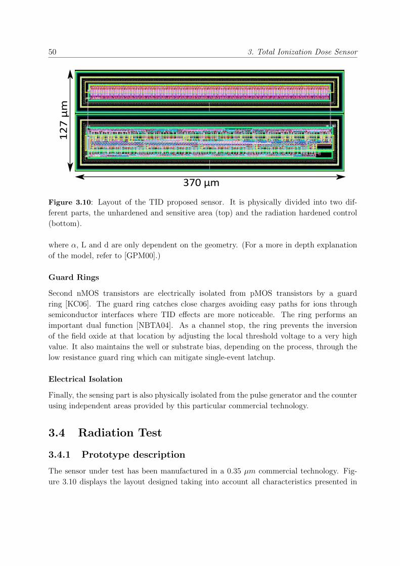
50 3. Total Ionization Dose Sensor
370 µm
12
7 µ
m
Figure 3.10: Layout of the TID proposed sensor. It is physically divided into two dif-
ferent parts, the unhardened and sensitive area (top) and the radiation hardened control
(bottom).
where α, L and d are only dependent on the geometry. (For a more in depth explanation
of the model, refer to [GPM00].)
Guard Rings
Second nMOS transistors are electrically isolated from pMOS transistors by a guard
ring [KC06]. The guard ring catches close charges avoiding easy paths for ions through
semiconductor interfaces where TID effects are more noticeable. The ring performs an
important dual function [NBTA04]. As a channel stop, the ring prevents the inversion
of the field oxide at that location by adjusting the local threshold voltage to a very high
value. It also maintains the well or substrate bias, depending on the process, through the
low resistance guard ring which can mitigate single-event latchup.
Electrical Isolation
Finally, the sensing part is also physically isolated from the pulse generator and the counter
using independent areas provided by this particular commercial technology.
3.4 Radiation Test
3.4.1 Prototype description
The sensor under test has been manufactured in a 0.35 µm commercial technology. Fig-
ure 3.10 displays the layout designed taking into account all characteristics presented in

3.4. Radiation Test 51
Table 3.1: Total Ionization Dose Sensor features.Area Percentage Energy per con-
version
Sensing 10400µm2 22% of sensor 300pJ
Logic 18910µm2 40% of sensor 163pJ
Physical Isolation 17680µm2 38% of sensor
Total Sensor 46990µm2 1.2% of ASIC 463pJ
Total ASIC 4mm2 100%
the previous section. In this layout, two main parts can be seen. On top the delay path
formed by a 256-inverter chain and at the bottom the pulse generator and the counter. As
shown, the radiation sensitive and insensitive parts are physically isolated. We fixed the
value of the counter constant to the maximum 4-bit pulse-count (16 pulses).
Table 3.1 summarizes the features of the manufactured prototype. In a small chip of
4 mm2, the sensor only requires 1% of the total area. Within the resources used for each
sensor, just the 22% is actually the sensitive part while the rest of the area is employed to
control and isolation. The overhead for radiation due to the RHBD techniques implemented
represent a high cost close to the 40% of the total area. Another remarkable figure is the
low energy per conversion required where the 66% corresponds to the sensitive area as the
control logic is idle when a conversion is not requested.
Seven Device Under Tests (DUTs) were fabricated and six of them were inserted in
a home-made breadboard and irradiated. The other DUT —DUT7— was treated as a
golden copy to compare the radiation effects with the normal configuration. Out of the
six irradiated chips, half of them were biased —DUT2, DUT3 and DUT6— and the other
half were unbiased —DUT1, DUT4 and DUT5— to test that unbiased chips were less
degraded by radiation effects [SSDF08]. The DUTs were biased at 3.3 V with a current
limit of 150 mA, by an Ethernet cable though an RJ45 interface. Figure 3.11 (b) shows
the board setup for the irradiation test, and Figure 3.11 (c) provides a closer look at the
DUTs disposition.
3.4.2 Test procedure
The test method to evaluate circuits in terms of total dose irradiation has been homogenized
and it is documented in the standard ESA-ESCC-22900. This standard is followed by most
of the players in the radiation tolerant electronic industry. We have also followed those
recommendations to measure our TID monitor.
Radiation tests were carried out at the NAYADE facility of CIEMAT in Madrid. This

52 3. Total Ionization Dose Sensor
(a) (b) (c)
Figure 3.11: Test set up for 60Co radiation test at CIEMAT.
facility fulfills all the requirements of the ESA-ESCC-22900. The pool of the facility appears
in Figure 3.11 (a). The 60Co source is placed at the pool bottom. The main characteristics
of this facility are:
• Type of source. 60Co cylindrical sources (15 mm diam. x 135 mm long) 12 sources
are distributed in a circular way providing an inner cylindrical irradiation volume.
Two distributions are available.
• High flux. 5 8.3 103Gy/h within a 60mm diameter x 100 mm long volume.
• Low flux. 5 1.2x10² Gy/h within a 200 mm diameter x 100 mm long volume.
• Irradiations at controlled temperatures and atmospheres, together with in-situ testing
of electrical properties available.
• In this device the irradiations can be carried out at controlled temperature up to
300◦C. A gas flow (as dry air or nitrogen) can be introduced during the irradiations
to prevent possible effect of humidity. The uncertainty dose rate is better than 20%
in a volume about 283 cm3.
• Dosimetry system. The routine gamma dosimetry is performed using the commer-
cially available Red PerspexTM 4034 Harwell dosimeters. These dosimeters have
shown to be valid in the range of 5 to 50 kGy and their accuracy is better than 10%.
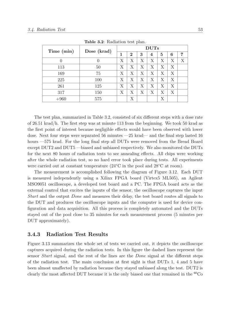
3.4. Radiation Test 53
Table 3.2: Radiation test plan.
Time (min) Dose (krad)DUTs
1 2 3 4 5 6 7
0 0 X X X X X X X
113 50 X X X X X X
169 75 X X X X X X
225 100 X X X X X X
261 125 X X X X X X
317 150 X X X X X X
+960 575 X X
The test plan, summarized in Table 3.2, consisted of six different steps with a dose rate
of 26.51 krad/h. The first step was at minute 113 from the beginning. We took 50 krad as
the first point of interest because negligible effects would have been observed with lower
dose. Next four steps were separated 56 minutes —25 krad— and the final step lasted 16
hours —575 krad. For the long final step all DUTs were removed from the Bread Board
except DUT2 and DUT5 —biased and unbiased respectively. We also monitored the DUTs
for the next 80 hours of radiation tests to see annealing effects. All chips were working
after the whole radiation test, so no hard error took place during tests. All experiments
were carried out at constant temperature (24◦C in the pool and 28◦C at room).
The measurement is accomplished following the diagram of Figure 3.12. Each DUT
is measured independently using a Xilinx FPGA board (Virtex5 ML505), an Agilent
MSO9051 oscilloscope, a developed test board and a PC. The FPGA board acts as the
external control that excites the inputs of the sensor, the oscilloscope captures the input
Start and the output Done and measures their delay, the test board routes all signals to
the DUT and produces the oscilloscope inputs and the computer is used for device con-
figuration and data acquisition. All this process is completely automated and the DUTs
stayed out of the pool close to 35 minutes for each measurement process (5 minutes per
DUT approximately).
3.4.3 Radiation Test Results
Figure 3.13 summarizes the whole set of tests we carried out, it depicts the oscilloscope
captures acquired during the radiation tests. In this figure the dashed lines represent the
sensor Start signal, and the rest of the lines are the Done signal at the different steps
of the radiation test. The main conclusion at first sight is that DUTs 1, 4 and 5 have
been almost unaffected by radiation because they stayed unbiased along the test. DUT2 is
clearly the most affected DUT because it is the only biased one that remained in the 60Co

54 3. Total Ionization Dose Sensor
RadgDosereached?
RemovegDUTsfromg
BreadgBoard
PlacegonegDUTgong
TestgBoard
RemovegDUTfromgTestgBoard
AllgDUTsghavegbeengmeasured?
PlacegDUTsgongBreadgBoard
ResumegRadiationexposition
No
Yes
Measuringgprocess
PCVirtexg5gML505
AgilentMSO9051
TestgBoardDUT
Figure 3.12: Diagram of measurement process.
chamber during the last step.
Differences in delay between the first measurements of each chip are due to process vari-
ations. All DUTs were manufactured within the same wafer, hence the process variations
that took place here were inter-die variations.
Figure 3.14 compares the simulation curve of the sensor with the results achieved
through the radiation test. Our sensor has been designed with a 4-bit counter and it
counts up to its maximum value —16 pulses. The simulation line reproduces the general
behavior of the sensor, but a more accurate estimation would require the use of our com-
mercial technology radiation data instead of the similar TSMC technology of [LOM+01].
Figure 3.15 is the result of the periodic measurements of the delay of DUT2 once the
radiation test is over. As can be seen, the delay measurement decreases after ceasing irra-
diation because of annealing taking place. The exponential curve is a good approximation
on how this effect behaves in our sensor as is proven by the residuals presented in the
bottom figure. The coefficient of determination is greater than 99% and the maximum
relative error of the fitting is less than 0.7%. This annealing process study proves that
the chip devices recover from radiation performance degradation. And, for example, a
forced annealing process could be used to restore devices performance through power and
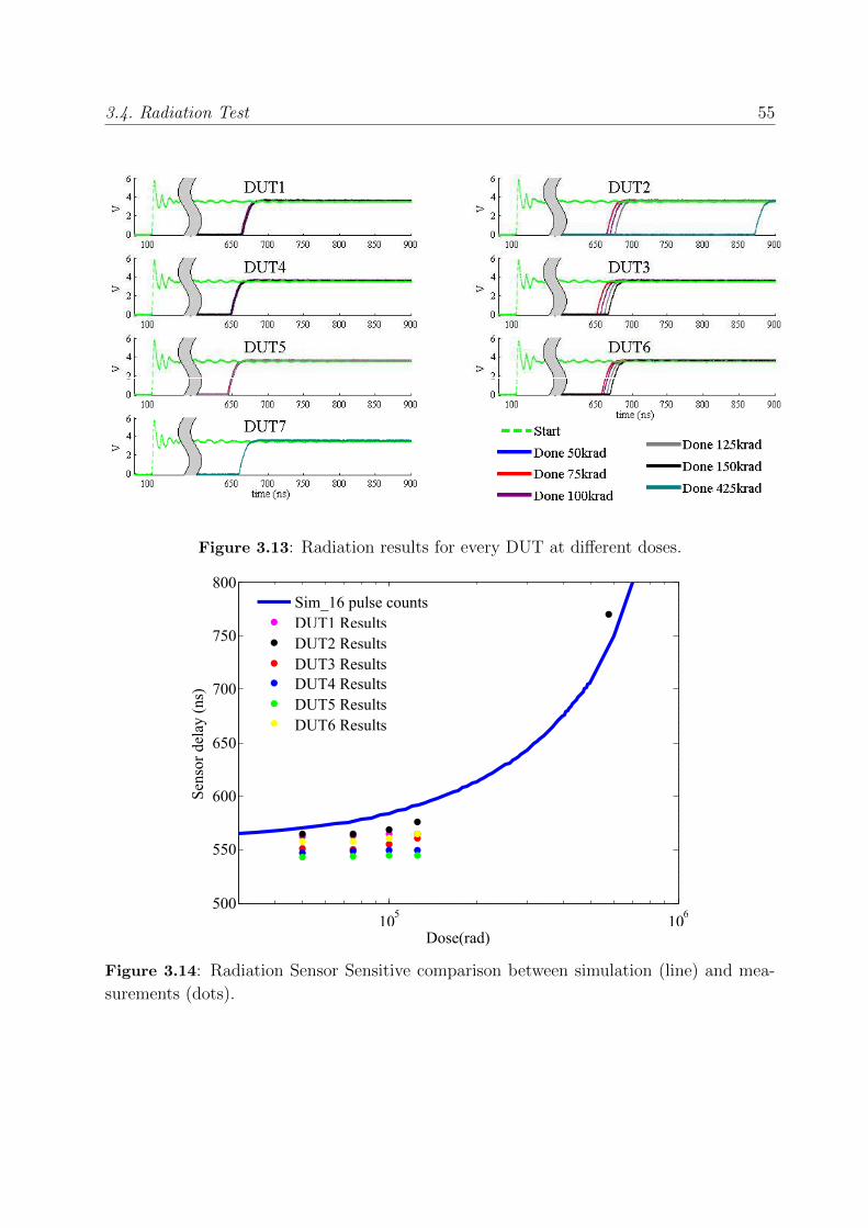
3.4. Radiation Test 55
Figure 3.13: Radiation results for every DUT at different doses.
105
106
500
550
600
650
700
750
800
Dose(rad)
Sen
sor
dela
y (n
s)
Sim_16 pulse countsDUT1 ResultsDUT2 ResultsDUT3 ResultsDUT4 ResultsDUT5 ResultsDUT6 Results
Figure 3.14: Radiation Sensor Sensitive comparison between simulation (line) and mea-
surements (dots).

56 3. Total Ionization Dose Sensor
0 10 20 30 40 50 60 70 80640
660
680
700
720
740
760
Annealing2time2(hours)
Sen
sor2
dela
y2(n
s)Test2ResultsExponential2fitting
0 10 20 30 40 50 60 70 80−4−2024
Annealing2time2(hours)Sen
sor2
dela
y2(n
s)E
rror
Residuals
R−square=0.9928
Figure 3.15: Delay time vs annealing time in DUT2. Test results, fitting curve and the
fitting errors.
Table 3.3: Board Power Consumption.
Dose accumulated (krad)
0 50 75 100 125 150 575
Current
(mA)10 10 20 30 50 60 90
temperature control as we will discuss in Section 3.8.
Additionally, we monitored the power consumption of the whole board during all radi-
ation steps, reported in Table 3.3. The power consumption increases along the radiation
tests because of the increase in leakage current. The value of this power consumption is
the addition of the different test vehicles included in the chip design, not only our sensor.
3.5 Temperature Test
3.5.1 Setup
Our sensor is based on a ring oscillator manufactured in a commercial technology, hence
it is expected that it is also sensitive to temperature. From [OILV13] the expression that
rules the delay td can be approximately:

3.5. Temperature Test 57
td ≈ k1CT (3.10)
were C is the number of delay elements, T the temperature and k1 is a process-dependent
parameter.
Once the radiation test and the annealing study are finished, we made a complete
temperature analysis to calibrate the readout of our radiation sensor. The tests were carried
out with a Votsch VCL 4010 [Ind] temperature chamber able to control the environment
temperature with an accuracy of 0.1 ◦C. The DUT package temperature is monitored by
a thermocouple to remove possible inaccuracies caused by self-heating while devices are
working. The hardware used for data acquisition is the same that was used for the radiation
test measuring process.
The temperature test consisted on the measurement of two different DUTs. The golden
DUT (DUT7) which was not exposed to radiation and DUT2, the most exposed. The
temperature was varied from 0 ◦C to 50 ◦C with 5 ◦C steps. Moreover, between 20 ◦C and
30 ◦C the steps were 2.5 ◦C for DUT2 and DUT7 because this range is the typical working
temperature where we want more accurate results. The temperature range was chosen
attending to the constraints of the commercial hardware used for data acquisition.
DUT7 was only measured with increasing temperature, starting at 0 ◦C and finishing
at 50 ◦C. But DUT2 was measured with increasing and decreasing temperature, forcing an
annealing stage between them during 6 hours at 50 ◦C. At 50 ◦C automatic measurements
were carried out every 10 minutes. These measurements consisted on taking 100 samples
in order to achieve a statistically correct result. The test plan is summarized in Table 3.4.
Table 3.4: Temperature test plan.
Temperature (Start -
Finish)Step DUT2 DUT7
0 ◦C - 20 ◦C 5 ◦C X X
20 ◦C - 30 ◦C 2.5 ◦C X X
30 ◦C - 50 ◦C 5 ◦C X X
6 hours at 50 ◦C 10 min X
50 ◦C - 30 ◦C 5 ◦C X
30 ◦C - 20 ◦C 2.5 ◦C X
20 ◦C - 0 ◦C 5 ◦C X

58 3. Total Ionization Dose Sensor
Figure 3.16: Oscilloscope measurements of the temperature tests.
0 10 20 30 40 50520
540
560
580
600
620
640
temperature5(ºC)
Sen
sor5
dela
y5(n
s)
DUT7DUT2_riseDUT2_fall
0 5 10 15 20 25 30 35 40 45 50-0.5
0
0.5
temperature5(ºC)
Err
orS
enso
r5de
lay5
(ns) DUT7 R-square=0.9993
DUT2_rise R-square=0.9992DUT2_fall R-square=0.9993
DUT75555555555--->51.02T+532.1DUT2_rise55--->51.28T+574.6DUT2_fall555--->551.25T+567.7
Figure 3.17: Temperature transfer function for our sensor design and its associated errors.

3.5. Temperature Test 59
0 50 100 150 200 250 300 350636
637
638
639
640
Annealing time (minutes)
Sen
sor
dela
y (n
s)
0 50 100 150 200 250 300 350−0.1
0
0.1
Annealing time (ns)
Err
orS
enso
r de
lay
(ns)
Residuals R−square=0.9927
meanstdlinear regressionmaximumminimum
td=−0.004t+637.8
Figure 3.18: Sensor response variation and its errors due to accelerated annealing at 50 ◦C.
3.5.2 Temperature Test Results
Figure 3.16 collects the oscilloscope captures of the temperature measurements. As was
expected, the delay increases with temperature for both, the golden and the irradiated
DUTs. The difference between DUT7 and DUT2 is due to the dose absorbed by radiation
exposure. And the difference between DUT2 heating and cooling is due to the annealing
process accelerated by the temperature stage at 50◦C. Another way of plotting the tem-
perature test results is shown in Figure 3.17. Here a linear regression and its error are
calculated.
The sensor has a temperature sensitivity of around 1 ns/◦C previous to radiation expo-
sure. After the dose accumulation, the sensitivity increases 20% and the offset 8%. The ac-
celerated annealing step recovers the slope by 2% and decreases the offset by 1%. These re-
sults indicate that TID effects can be reversible [KLA96] and high temperatures accelerate
the recovering of radiation-induced degradation in electronic systems [GMG+15,HKM16].
Of course, high temperatures potentially damage electronic circuits so the temperature
range is limited by devices constraints.
The acceleration of the annealing process at 50 ◦C in DUT2 is shown in Figure 3.18
where upper and lower lines represent the maximum and minimum value of the 100 sam-
ples. Curve fitting approximation corresponds to a linear regression because this measure-
ment was made after annealing monitoring for 80 hours, corresponding to the end of the
exponential fitting of Figure 3.15.

60 3. Total Ionization Dose Sensor
0
20
40
60 103
104
105
106
500
600
700
800
900
y(rad)TIDTemperaturey(ºC)
Sen
sory
dela
yy(n
s)
t27
Figure 3.19: Representation of Equation 3.11 for DUT2 with measured data.
3.6 Calibration
Based on our experimental analysis, we propose the following model for the sensor delay:
td = t27 + α ∗ (T − 27) + trad27(TID) + β(TID) ∗ (T − 27) (3.11)
where t27 is the fresh delay at room temperature, α is the fresh delay slope caused by
temperature, T is the temperature, trad27(TID) is the delay caused by the TID at room
temperature, and β is the change in the delay slope caused by the TID. Figure 3.19 shows
the data measured for our DUT2 sensor, and represents graphically each of the previous
parameters.
If we want to extract TID from this equation, first we need to know the value of
the current temperature, which can be provided by a different temperature sensor. And
second, due to process variations and the uncertainties of the irradiation absorption, α,
t27, trad27(TID) and β(TID) are unknown and must be obtained by means of a calibration
process.
Concerning α and t27, they can be extracted through a two-point calibration process
on the fresh circuit, one at room temperature to extract t27, and another at a different
temperature to obtain α.
As far as trad27(TID) and β(TID) are concerned, these complex functions actually
need irradiating the circuit with a well calibrated source to be obtained. As this is a
destructive process, since the sensor only recovers partially from the degradation induced by
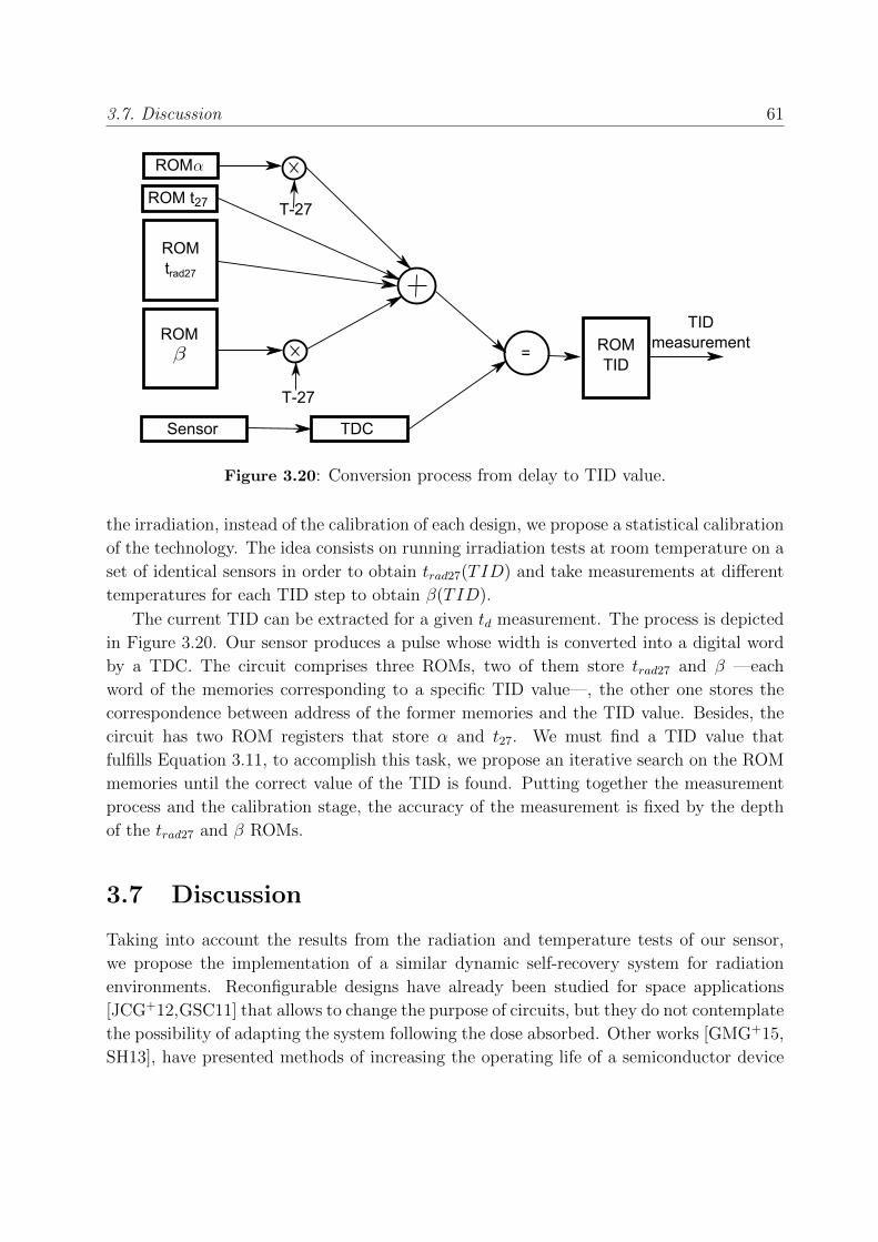
3.7. Discussion 61
ROM t27
ROM
ROMtrad27
ROM=
Sensor TDC
ROMTID
TIDmeasurement
T-27
T-27
Figure 3.20: Conversion process from delay to TID value.
the irradiation, instead of the calibration of each design, we propose a statistical calibration
of the technology. The idea consists on running irradiation tests at room temperature on a
set of identical sensors in order to obtain trad27(TID) and take measurements at different
temperatures for each TID step to obtain β(TID).
The current TID can be extracted for a given td measurement. The process is depicted
in Figure 3.20. Our sensor produces a pulse whose width is converted into a digital word
by a TDC. The circuit comprises three ROMs, two of them store trad27 and β —each
word of the memories corresponding to a specific TID value—, the other one stores the
correspondence between address of the former memories and the TID value. Besides, the
circuit has two ROM registers that store α and t27. We must find a TID value that
fulfills Equation 3.11, to accomplish this task, we propose an iterative search on the ROM
memories until the correct value of the TID is found. Putting together the measurement
process and the calibration stage, the accuracy of the measurement is fixed by the depth
of the trad27 and β ROMs.
3.7 Discussion
Taking into account the results from the radiation and temperature tests of our sensor,
we propose the implementation of a similar dynamic self-recovery system for radiation
environments. Reconfigurable designs have already been studied for space applications
[JCG+12,GSC11] that allows to change the purpose of circuits, but they do not contemplate
the possibility of adapting the system following the dose absorbed. Other works [GMG+15,
SH13], have presented methods of increasing the operating life of a semiconductor device
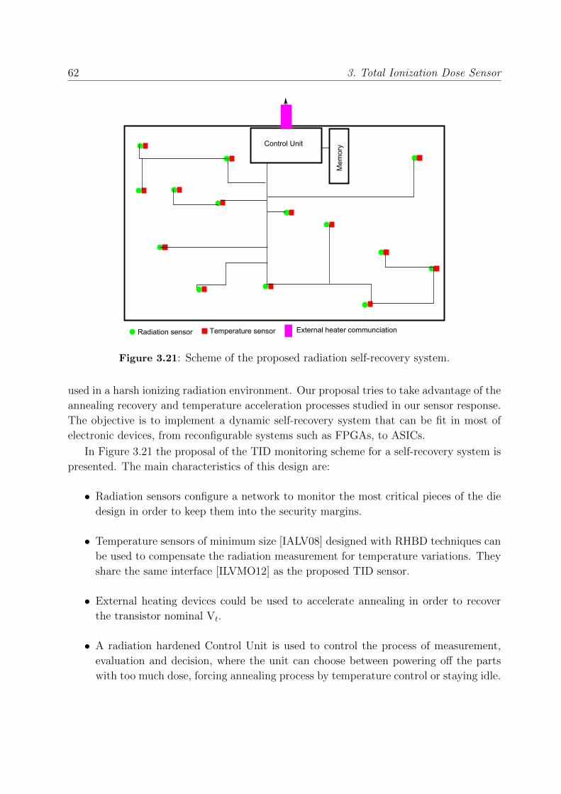
62 3. Total Ionization Dose Sensor
Mem
ory
Control Unit
Radiation sensor Temperature sensor External heater communciation
Figure 3.21: Scheme of the proposed radiation self-recovery system.
used in a harsh ionizing radiation environment. Our proposal tries to take advantage of the
annealing recovery and temperature acceleration processes studied in our sensor response.
The objective is to implement a dynamic self-recovery system that can be fit in most of
electronic devices, from reconfigurable systems such as FPGAs, to ASICs.
In Figure 3.21 the proposal of the TID monitoring scheme for a self-recovery system is
presented. The main characteristics of this design are:
• Radiation sensors configure a network to monitor the most critical pieces of the die
design in order to keep them into the security margins.
• Temperature sensors of minimum size [IALV08] designed with RHBD techniques can
be used to compensate the radiation measurement for temperature variations. They
share the same interface [ILVMO12] as the proposed TID sensor.
• External heating devices could be used to accelerate annealing in order to recover
the transistor nominal Vt.
• A radiation hardened Control Unit is used to control the process of measurement,
evaluation and decision, where the unit can choose between powering off the parts
with too much dose, forcing annealing process by temperature control or staying idle.
3.8. Conclusions 63
• Rad-hard memories perform the conversion of radiation and temperature measure-
ments according to the proposed calibration methodology.
• An interesting point is that calibration might be unnecessary if the sensor network
goal is monitoring the degradation of electronics in different parts of the circuit. In
this case, controlling the delay shift is enough, thus TID conversion can be skipped.
Using this scheme, an example of its operation would be: the control unit sweep peri-
odically the measurement of each radiation sensor to monitor the absorbed dose of each
part of the circuit. Each measurement needs to monitor the adjacent temperature sensor
that compensates the variation of the radiation sensor due to temperature. If the dose
absorbed is above the limit of secure operation, then the control unit is able to apply
different policies to recover the system. These policies could be: stop the system, stop
just a part close to the affected area, heating the system to accelerate the annealing or use
micro-heaters to recover just the most radiated zone.
In the implementation of this type of systems, the overhead of designing an additional
sensor network is desirable to be as small as possible and the power consumption should
have a very small impact in the consumption of the whole design. Hence, both character-
istics are perfectly fulfill by our TID built-in smart sensor.
3.8 Conclusions
In this chapter, a TID sensor has been designed, manufactured, radiated and characterized.
It is a digital CMOS sensor based on the relationship between the accumulated radiation
and the performance degradation of the frequency in ring oscillators. The bigger the dose
absorbed, the slower the ring oscillator frequency. The main advantages of this sensor
compared to RADFET, the reference sensor used by nearly all applications, is that our
design actually measures the dose absorbed by an electronic circuit instead of the amount
of radiation it has been exposed to.
The design of the sensor has been divided into two different areas, the sensitive part
and the control logic. As the control logic needs to be robust against radiation, RHBD
mitigation techniques have been used to harden this block.
Extensive experimental tests have been carried out to fully characterize the proposed
sensor. In the radiation tests biased DUTs have shown a response that matches their
expected behavior under radiation while unbiased sensors were almost immune to TID
effects. Charge redistribution has been also observed after the radiation test what supports
the possibility of implementing dynamic recovery systems.
Additionally to the radiation characterization, we have characterized the sensor in terms
of temperature sensitivity to be able to compensate the deviation produced by temperature
64 3. Total Ionization Dose Sensor
variation. The sensor proved to be almost linearly dependent on this magnitude, hence
easy to compensate by a previous calibration. A calibration system has also been proposed.
It is based on the use of memories, adders and multipliers that remove the radiation
measurement deviation.
The main features of our prototype are: small size, low power consumption, fully
integrable, digital interface and configurable sensitivity. All of them make our proposal
suitable for its implementation in every circuit that needs to monitor the dose absorbed
in order to maintain the devices in safe operation conditions. The versatility of the design
makes it possible to use in all kind of electronic systems. Moreover, the control of actual
absorbed dose can be used to implement a self-recovery system using heaters to force
annealing in the affected areas.
3.9 Related Publications
• J. Agustin, C. G. Soriano, M. L. Vallejo and P. Ituero, ”A built-in CMOS Total
Ionization Dose smart sensor,” IEEE SENSORS 2014 Proceedings, Valencia, 2014,
pp. 70-73. doi: 10.1109/ICSENS.2014.6984935
• J. Agustin, C. Gil, M. Lopez-Vallejo and P. Ituero, ”Design and Characterization
of a Built-In CMOS TID Smart Sensor,” in IEEE Transactions on Nuclear Science,
vol. 62, no. 2, pp. 443-450, April 2015. doi: 10.1109/TNS.2015.2404532

Chapter 4
Efficient Mitigation of SETInduced Harmonic Error

Chapter 4
Efficient Mitigation of SET InducedHarmonic Error
4.1 Introduction
Soft errors are an important source of fault injection that reduces the reliability of modern
nanometer technologies [SYW13]. Since the detection of first radiation induced soft errors,
SEUs were the principal contribution to the system errors. Therefore, many different ap-
plications and solutions have been investigated and proposed for the hardening of this kind
of effects. On the other hand, SETs were not considered so important because they were
mostly masked without altering any output of the systems. However, technology scaling
has enhanced the severity and relevance of SET effects. The occurrence and propagation
of SETs increases as geometric dimension and capacitance scale down, while the probabil-
ity of SET capture grows with higher operational frequencies [FCMG13]. Therefore, for
the last decade, SETs have emerged as the main contribution to soft error rate in elec-
tronics [HA13]. Consequently, SET research has became an important topic in radiation
effects field. Nowadays, many efforts are focused on studying of the phenomenon through
experimental observation, modeling and simulation at different levels of abstraction.
The study of SETs has been closely linked to the impact of this transitory effect into a
chain of inverters [FCPM+07, GAN+10] because they are a simple enough structure that
allows to easily understand the basic mechanisms of the generation and propagation of
SETs. Recent works have observed that SETs can cause the shift of the output oscillation
from the fundamental frequency to an odd harmonic in ring oscillators [CBN+09]. And
it has been also reported an analytical harmonic window model [C+14] that characterizes
those harmonic induced errors and sets the conditions that ring oscillators and SETs must
fulfill together in order to be affected by this phenomenon. Since the frequency shift
produced by the odd harmonic appearance may result in system errors, synchronization
problems or SEFIs, it is necessary to harden the design of ring oscillators for radiation
applications.
This chapter is focused on completely removing the harmonic induced errors in ring
oscillators by an effective design with negligible area overhead. To accomplish this task,
we propose a new design of ring oscillators that makes use of asymmetric stages in order

4.2. Single Event Transients in Electronics 67
to force the electrical masking of the SET pulse induction. The asymmetric design confers
the ability of configuring the duty cycle on the ring oscillator outputs. The hypothesis of
harmonic removal using this new approach has been validated by two different methods:
Firstly by the simulation of SET injection with a 40 nm commercial technology. Secondly
by the measurement of SET emulation into two different manufactured test circuits. These
designs are implemented with a 0.35 µm commercial technology. To guarantee a SET oc-
currence in the ring oscillator test circuits, instead of taking a very expensive radiation test
campaign, we have designed a SET emulation injection based on forcing a third harmonic
oscillation by introducing three different enabled nodes instead of just one. The emulated
SET satisfies all the conditions [C+14] required to provoke a third harmonic shift, but as
was expected, our design fully masks them all. Therefore, the model has been validated
with two different technologies and topologies.
The rest of the chapter is organized as follows: First in Section 4.2, the SET effects are
explained from the physical basics to the testing methods. Section 4.3 summarizes the an-
alytical model of Chen et al. [C+14] for the induction of harmonic errors in ring oscillators.
After that, the SET-removal proposal is presented and characterized in Section 4.4. Then
the model and the proposed SET mitigation strategy is simulated in Section 4.5. The man-
ufactured prototype and the designed SET emulation system are described in Section 4.6.
Section 4.7 deals with the validation of the model through electrical measurements. And
finally Section 4.8 concludes with the main contributions of this chapter.
4.2 Single Event Transients in Electronics
4.2.1 Introduction
When an energetic nuclear particle hits a semiconductor structure, it loses energy through
the interaction with the material lattice structure. Unlike TID which causes the permanent
degradation of device parameters, a single event is an instantaneous effect. As the charged
particles pass through the material, the ions generate electron-hole pairs through their
path. Those free electrons and holes liberation creates an unexpected electric current in
the semiconductor device. That induced electric current is the foundation of all SEEs.
Attending to the effect produced by that transient current, SEEs are classified according
to the list presented in Chapter 2 (SEU, SET, SEFI, etc.). Among all of these effects, this
chapter is focused on solving a SET effect in ring oscillators, which can be considered the
source of all other effects.
There are three stages involved in the formation of SETs: charge generation, charge
collection and circuit response. The charge generation is defined as the amount of electron-
hole pairs generated by the particle hit and it depends on the LET of the incident ion. The
charge collection includes the process of charge redistribution and diffusion. It depends on
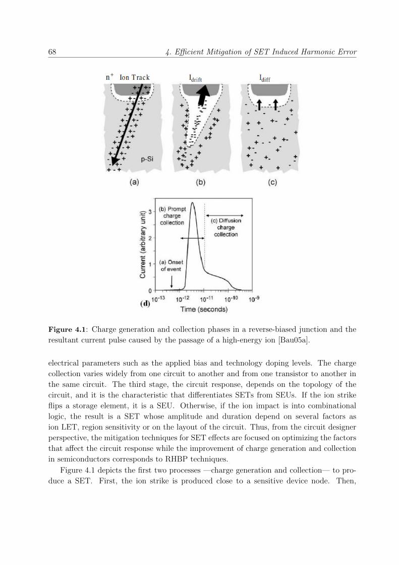
68 4. Efficient Mitigation of SET Induced Harmonic Error
Figure 4.1: Charge generation and collection phases in a reverse-biased junction and the
resultant current pulse caused by the passage of a high-energy ion [Bau05a].
electrical parameters such as the applied bias and technology doping levels. The charge
collection varies widely from one circuit to another and from one transistor to another in
the same circuit. The third stage, the circuit response, depends on the topology of the
circuit, and it is the characteristic that differentiates SETs from SEUs. If the ion strike
flips a storage element, it is a SEU. Otherwise, if the ion impact is into combinational
logic, the result is a SET whose amplitude and duration depend on several factors as
ion LET, region sensitivity or on the layout of the circuit. Thus, from the circuit designer
perspective, the mitigation techniques for SET effects are focused on optimizing the factors
that affect the circuit response while the improvement of charge generation and collection
in semiconductors corresponds to RHBP techniques.
Figure 4.1 depicts the first two processes —charge generation and collection— to pro-
duce a SET. First, the ion strike is produced close to a sensitive device node. Then,

4.2. Single Event Transients in Electronics 69
the particle generates radial distribution of electron-hole pairs such as in Figure 4.1 (a).
The charge distribution induces a temporary funneling effect where some charges are re-
combined but most of them are redistributed (Figure 4.1 (b)). The funneling effect lasts
around tens of picoseconds, after what, the diffusion dominates the redistribution of charges
in Figure 4.1 (c). Diffusion could last about nanoseconds. The combination of all these
processes results in a current pulse at the junction as illustrated in Figure 4.1 (d). The
current transient typically lasts hundreds of picoseconds.
Regarding the circuit response, not all generated SETs in a circuit are visible at the
outputs. Even an ion with enough energy and striking into a very sensitive area inducing
a high current can be mitigated. When this occurs, the SET is masked. There are three
factors that determine whether an SET will propagate and result in an error:
• Logical masking. A SET is masked due to the value of the other inputs. For example,
in Figure 4.2 (a,c), the outputs are not switched while the same hit node with different
inputs in Figure 4.2 (b,d) swing.
(a) (b)
(c) (d)
10 1
1 00
Figure 4.2: Logical Masking (a and c) and propagation (b and d) of SET by NAND and
NOR gates.
• Electrical masking. It refers to the process whereby the induced current propagates
through a combinational path. The spontaneous glitch is able to propagate just
through a finite number of stages. The reason is that the slopes of the ion current
are greater than the delay of combinational logics and therefore, the gate cannot
drive the next node at that speed, degrading the pulse as in Figure 4.3.
• Temporal masking. SETs are only an issue if at the end of the combinational path
the glitch is latched into a register. So, there is only a vulnerability window in which
the glitch can be converted into a SEU. In Figure 4.3 the two different scenarios are
presented (latched and non-latched).
The increasing relevance of SETs with shrinking technology nodes can be explained
through the analysis of the dependency of technology into masking effects. First, the

70 4. Efficient Mitigation of SET Induced Harmonic Error
11
1
1
Figure 4.3: Electrical masking of SET due to the propagation delay of combinational
gates.
output
clock
input
masked error
Figure 4.4: The temporal masking of SETs depends on the vulnerability window of reg-
isters.
implementation of transistors with smaller dimensions increases the density of active zones
in system layouts what increases the probability of an ion track to impact in sensitive nodes.
Second, the smaller capacitance of nodes facilitates wider induced pulsewidths. Third,
the electrical masking decreases with wider pulsewidths and faster gates. Finally, the
temporal masking is also reduced because the vulnerability windows increases with higher
frequencies. The vulnerability window is defined as the relationship between the part of
the clock period where a glitch makes the output swing with the part where it is unaltered.
This value is determined by the setup and hold times of registers and the frequency. Set
up and hold times decrease with technology but not as much as the operational period.
Therefore, the affected ratio increase significantly. The addition of these effects has made
SET the major contribution to the Single Event Rate (SER) in modern circuits.
4.2.2 Testing
Routine SEE testing in real operation conditions is impractical because of three main
reasons:
• The integration of devices into space experiments are extremely expensive and the
access is highly limited due to the small amount of missions and the high demand of
area in spacecrafts.
• The control of the impact particles to sensitive regions for testing critical points in
electronic designs is unfeasible due to the randomness of natural environments.

4.2. Single Event Transients in Electronics 71
Table 4.1: Guidelines ans Standards for SEEs testing.Test Standard Description Source
JESD57 Test Procedures for the Measurement of
Single-Event Effects in Semiconductor De-
vices from Heavy Ion Irradiation
Heavy Ions
JESD89 Test guideline for Alpha and Neutron SEE
testing
Alpha and
Neutrons
ASTM F-1192 Test guideline for heavy ion testing Heavy Ions
ESCC 25100 ISSUE 1 SEE testing of integrated circuits and dis-
crete semiconductors devoted to space appli-
cations
Protons
and Heavy
Ions
• The time required to perform an in-depth characterization would take a long time
using the fluxes presented in ground or space environments.
Therefore, testing is done using ground facilities. Although every facility offers differ-
ent kinds of test, all of them obey the guidelines approved by standard organization to
homogenize their results. There are different guidelines and standards to test and charac-
terize electronic components and circuits in terms of SEE response. The most important
procedures are outlined in Table 4.1. The approved methods to test SEE use accelerators,
radioactive sources and pulsed lasers. Each of these techniques has its own strengths and
limitations.
Accelerators
Most SEE testing is done at accelerators with relatively low-energy ions (tens of MeV/amu)
because of the much greater cost and more limited accessibility of high-energy ion accel-
erators [GRD+16, CLT+14]. Because low-energy ions are unable to pass through thick
material, packaged parts must be delidded and placed in a vacuum chamber.
Although accelerators are necessary for SET testing, they do not, in general, provide
any spatial or temporal information about the origins of SETs, which restricts their use to
qualifying parts rather than obtaining detailed information about the actual mechanisms
responsible for SETs [PBS+16].
Radioactive Sources
Radioactive sources (Cf252 [YYCS14,EHA+15] and Am241 [ZJA+16,MGJ+13]) may be used
for laboratory measurements of SET sensitivity. Cf252 is more widely used in the space
community because the ions emitted from the nucleus have higher LETs than the alpha
72 4. Efficient Mitigation of SET Induced Harmonic Error
particles emitted by Am241. Unfortunately, both radioactive sources emit ions with limited
range and, in the presence of passivation layers, the ions are not able to reach the sensitive
volume in which SETs are generated. In addition, for detailed studies of SET mechanisms,
the technique does not provide spatial information, although some temporal information
may be obtained from time-of-flight measurements.
Pulsed Lasers
The pulsed laser has been used successfully to investigate the nature of SETs in both
analog and digital integrated circuits [SFW+16, AHG+13]. A pulsed laser is well suited
for studying SETs because the beam of light can be focused to a spot about a micron
in diameter and positioned on any desired location in the circuit to inject SEEs. Pulsed
laser light produces no radiation damage in the semiconductor. This makes it possible to
probe in detail SET-sensitive regions in the circuit for which it is necessary to irradiate
for long periods of time. Another feature of pulsed laser testing is that the arrival time of
the light pulse can be adjusted relative to the circuit clock [BMPM13], a capability needed
for measuring frequency dependent capture probabilities of SETs in latches. Additional
useful features are that the technique requires no vacuum and it is convenient because
it can be used in both laboratory and fabrication facilities. There are two limitations
to this technique. One is that metal layers and multilayer dielectrics interfere with the
transmission of the light, further complicating the establishment of a reliable and accurate
threshold energy. And the other is that, in very dense circuits with the minimum feature
size less than the diameter of the focused light beam, it is unlikely that SET thresholds
can be obtained.
4.2.3 SET Modeling
Testing is a mandatory stage to assure the reliability of circuits. However, the cost of test
campaigns is so expensive that testing every prototype is not affordable. In order to be
able to preview the effects of SETs in circuits, different models have been developed. In
general, the role of modeling is to provide designers with a set of tools that they may be
used to:
• Better understand the physical mechanisms.
• Analyze and predict the results of testing.
• Develop appropriate hardening strategies.
A commonly used analytical model to simulate the induced transient current waveform
is the double-exponential function with a fast rise time and a slower fall time [BRW+15].

4.3. SET Induced Harmonic Errors in Ring Oscillators 73
This model has been validated with many different technologies [WVK07,CRL+03,WVNK08]
and it is the most used in transistor-level simulations.
I(t) =
0 t < td1
Ipeak
(1− e
−(t−td1)
τ1
)td1 < t < td2
Ipeak
(e
−(t−td2)
τ2 − e−(t−td1)
τ1
)td2 < t
(4.1)
where td1, is the onset of the rise of the current, td2 is the onset of the fall of the current,
Ipeak is the maximum current to be approached, τ1 is the rise time constant, and τ2 is the
fall time constant
Recent studies have improved the model for nanometer technologies. In technologies
under hundreds of nm, a new effect has appeared in the charge collection process when
a transistor is embedded into a combinational path. Instead of a double exponential, in
the middle of the falling step, it exists an interval where the induced current remains
almost constant as can be seen in Figure 4.5. This phenomenon named “plateau” has been
attributed to the collapse of potential at the struck junction and a subsequent balance
of charge collection current and resupply current from the restoring device [DWB+07].
This effect has been shown to be critically important to the SET pulsewidths under for
technologies 100-nm.
To translate this behavior into a circuit discrete component to be integrated in a
transistor-level model, in [BRW+15] a dual double exponential current source is proposed.
The “plateau” phenomenon can be modeled by two components: a long double-exponential
current source equal to the shelf current and a short double-exponential current source to
add the extra current for the short peak. [BRW+15] validates this double source model
against an IBM 90 nm technology and more recently, [QXW+16] has also applied this
model to a 65 nm commercial technology.
4.3 SET Induced Harmonic Errors in Ring Oscillators
Once the SET effect has been introduced, this Section analyzes the problem that this kind
of radiation effects produces in ring oscillators. Ring oscillators are formed by a chain of
inverter gates connected in a loop configuration. Since they are made of combinational
logic, they are not affected by SEUs. But, at the same time, the loop configuration enables
the lock of a SET in the circuit and, consequently, a persistent error instead of a transient
glitch.
If a SET induced current is produced in a node of a ring oscillator, then its output can
change its properties. Casey et al. [CBN+09] outlined the potential consequences of a SET
impact in a ring oscillator. They used laser strikes at different energies to induce SETs

74 4. Efficient Mitigation of SET Induced Harmonic Error
Figure 4.5: Plateau effect presented in [DWB+07] as a consequence of SETs in technologies
under 100 nm.
SET hit
time
Amplitude
GND
VDD
time
Amplitude
GND
VDD
(a)
(b)
Figure 4.6: SET impact in a ring oscillator and the potential 3rd (a) and 5th (a) induced
harmonic oscillations.
and they conclude that a SET in a ring oscillator can shift the output frequency to an odd
harmonic of the fundamental oscillation as can be seen in Figure 4.6.

4.3. SET Induced Harmonic Errors in Ring Oscillators 75
In addition, Chen et al. [C+14] observed that the harmonic induced oscillation can be
transitory or it can be permanently changed. To define those possibilities they developed
an analytical model called “Harmonic Vulnerability Window” model. That model sets the
requirements that a SET must fulfill to produce and sustain the third harmonic induced
error in a Digitally Controlled Ring Oscillator. In that work, the next assumptions and
notations are made:
• A ring oscillator consists of N inverter gates with propagation delays (td0, ..., tdi, ..., td(N−1)).
• The period of the output clock signal is:
T/2 = td0 + ...+ tdi + ...+ td(N−1) (4.2)
• The maximum propagation delay (tdmax) is defined by:
tdmax = max{td0, ..., tdi, ..., td(N−1)} (4.3)
Using these assumptions, the three requirements for maintaining the third harmonic
oscillation in a steady state are:
1) The SET must introduce one rising edge and one falling edge transition within half
the oscillation period.
This condition defines a maximum limit for a SET induced pulsewidth (tSET ). If it is
greater than this limit, the impact at the output is an increased instant skew.
2) tSET should be greater than the largest gate propagation delay in the ring oscillator.
tSET > tdmax = tSET (min) (4.4)
Otherwise the SET would be electrically masked by the slowest gate. This condition defines
a minimum limit.
3) tSET should be smaller than the total loop delay (L) minus two times tdmax.
Furthermore, if ta and tb are defined at the hit node as the time between one clock edge
and the start of SET and between the end of the SET and the other clock edge according
to Figure 4.7, then the upper limit is adjusted by:
ta > tdmax and tb > tdmax (4.5)
tSET (max) = L− ta − tb < L− 2tSET (min) < L− 2tdmax (4.6)
If any of all of these times is violated, then the SET is electrically masked in a few
clock cycles.
The three initial assumptions include the case of different tdi but they suppose a ring
oscillator formed by balanced gates in which the fall delay time (tdfall) and rise delay time
(tdrise) are equal. The solution proposed in this thesis does not meet this assumption, so
the “Harmonic Vulnerability Window” model will be reformulated in an unbalanced ring
oscillator.

76 4. Efficient Mitigation of SET Induced Harmonic Error
Figure 4.7: SET pulse parameters defined in [C+14] for Induced Harmonic Errors charac-
terization.
4.4 Proposed Solution
Considering the three requirements of SET harmonics introduced in [C+14], our goal is
designing a ring oscillator whose output lacks of the vulnerability window of Figure 4.7.
To accomplish this task, this thesis devises a procedure that generates an output with a
duty cycle that is not 50% and it is big enough to overlap ta and tb. Then the SET would
be electrically masked as the three requirements previously assumed are not fulfilled. This
design also avoids the induction of higher harmonics [Cas10] but from now on, the chapter
will be focused on the third harmonic to validate the concept. In this Section the schematic
of the proposal and its mathematical analysis is introduced to understand the behavior.
The explanation of the SET mitigation process is described in the next Section.
The proposed solution is based on the ring oscillator schematic of Figure 4.8. This ring
oscillator is made of an odd number, N, of gate inverters. All transistor gate lengths (L) are
the minimum allowed by the technology. The difference with conventional ring oscillators
is the introduction of asymmetry in the design of transistor aspect ratios which results in
unbalanced ring stages (tdfall 6= tdrise). The N nodes are divided into odd and even nodes.
At odd nodes, the pMOS devices are larger than the nMOS devices and therefore can sink
more current than the nMOS devices. As a result, the pull-up path (tdorise) is faster than
the pull-down path (tdofall)(tdofall > tdorise). Even nodes are designed upside down with
a smaller pMOS (Wpe) and a larger nMOS (Wne). Then, at even nodes, the pull-up path
(tderise) is slower than the pull-down path (tdefall) (tdefall < tderise).
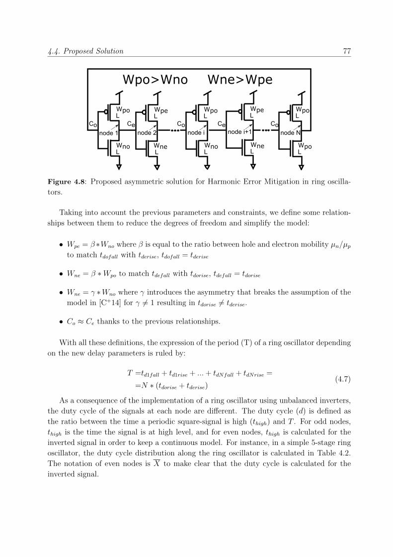
4.4. Proposed Solution 77
Co Co CoCe Cenode 1 node 2 node i node i+1 node N
WpoL
WpeL
WnoL
WneL
WpoL
WnoL
WpeL
WneL
WpoL
WpoL
Wpo>Wno Wne>Wpe
Figure 4.8: Proposed asymmetric solution for Harmonic Error Mitigation in ring oscilla-
tors.
Taking into account the previous parameters and constraints, we define some relation-
ships between them to reduce the degrees of freedom and simplify the model:
• Wpe = β ∗Wno where β is equal to the ratio between hole and electron mobility µn/µpto match tdofall with tderise, tdofall = tderise
• Wne = β ∗Wpo to match tdefall with tdorise, tdefall = tdorise
• Wne = γ ∗Wno where γ introduces the asymmetry that breaks the assumption of the
model in [C+14] for γ 6= 1 resulting in tdorise 6= tderise.
• Co ≈ Ce thanks to the previous relationships.
With all these definitions, the expression of the period (T) of a ring oscillator depending
on the new delay parameters is ruled by:
T =td1fall + td1rise + ...+ tdNfall + tdNrise =
=N ∗ (tdorise + tderise)(4.7)
As a consequence of the implementation of a ring oscillator using unbalanced inverters,
the duty cycle of the signals at each node are different. The duty cycle (d) is defined as
the ratio between the time a periodic square-signal is high (thigh) and T . For odd nodes,
thigh is the time the signal is at high level, and for even nodes, thigh is calculated for the
inverted signal in order to keep a continuous model. For instance, in a simple 5-stage ring
oscillator, the duty cycle distribution along the ring oscillator is calculated in Table 4.2.
The notation of even nodes is X to make clear that the duty cycle is calculated for the
inverted signal.

78 4. Efficient Mitigation of SET Induced Harmonic Error
Table 4.2: 5-Stage ring oscillator duty-cycle distribution.
node thighthighthigh tlowtlowtlow TTT ddd
1 4tdorise + tderise 4tderise + tdorise 5tderise + 5tdorise4tdorise + tderise
5(tderise + tdorise)
2 3tdorise + 2tderise 3tderise + 2tdorise 5tderise + 5tdorise3tdorise + 2tderise5(tderise + tdorise)
3 2tdorise + 3tderise 2tderise + 3tdorise 5tderise + 5tdorise2tdorise + 3tderise5(tderise + tdorise)
4 tdorise + 4tderise tderise + 4tdorise 5tderise + 5tdorisetdorise + 4tderise
5(tderise + tdorise)
5 5tderise 5tdorise 5tderise + 5tdorise5tderise
5(tderise + tdorise)
If we generalize the expression of the duty cycle (column d) to a ring oscillator of N
stages, the equation that rules the duty cycle is:
di =(N − i)(tdorise) + i(tderise)
N(tdorise + tderise)(4.8)
This equation is based on the assumption that different duty cycles in a ring oscillator
is correct. It also matches to the conventional ring oscillators based on balanced gates
(tdofall = tderise = tdefall = tdorise) and an output duty cycle of 50%.
Figure 4.9 plots the simulated signal of four internal nodes of a 15-stage ring oscillator
with γ = 4. As can be seen, the values of the duty cycles are approximately 80%, 65%,
50%, and 20% as calculated from Equation 4.8. We simulated a bigger ring oscillator of
99-stage using commercial 40 nm technology models to get more accurate results. Fig-
ure 4.10 compares the results of the theoretical and simulated duty cycle distributions of
that ring oscillator with different γ values. An important characteristic shown by both,
the theoretical study and the simulations, is that there is always a node with a 50% duty
cycle which can be used as a clock signal or as the conventional output ring oscillators
usually provide. The analytical model is a simple model that only considers the transistor
gate capacitances. Although it is a very simple model, the maximum absolute error is less
than 2%, proving the fundamental behavior of the design.
The main drawback of this proposal is the maximum achievable frequency of the ring
oscillator. Since the implemented transistors are asymmetric and different from the fastest
design, the maximum frequency is indirectly proportional with respect to γ. Concerning

4.4. Proposed Solution 79
0
1
0
1
Am
plit
ude
(V)
0
1
time (ns)0 1 2 3 4 5 6
0
1
2tdefall
3tdefall
5tdefall
2tderise
3tderise
5tderise
node 3
node 13
node 8
node 5
Figure 4.9: Internal nodes (3, 5, 8, 13) of a 15-stage ring oscillator where different duty
cycles are observed.
. =6
. =7
. =8
=9. =10
. =6
. =7
. =8
. =9
. =10
. =6
. =7
. =8
. =9
. =10
.=6
.=7
.=8 .
=9
.=10
order of nodes10
duty
cyc
le (
%)
90
=1
=2
=3
=6
=10
80
70
60
50
40
30
20
1020 30 40 50 60 70 80 90 100
=4
Figure 4.10: 99-stage ring oscillator duty cycle distribution for different γ ratios. Dotted
lines are theoretical results and solid lines are simulation results.
to the phase noise and jitter measurements, our simulations show the same behavior as
conventional ring oscillator with a difference of less than 1%.
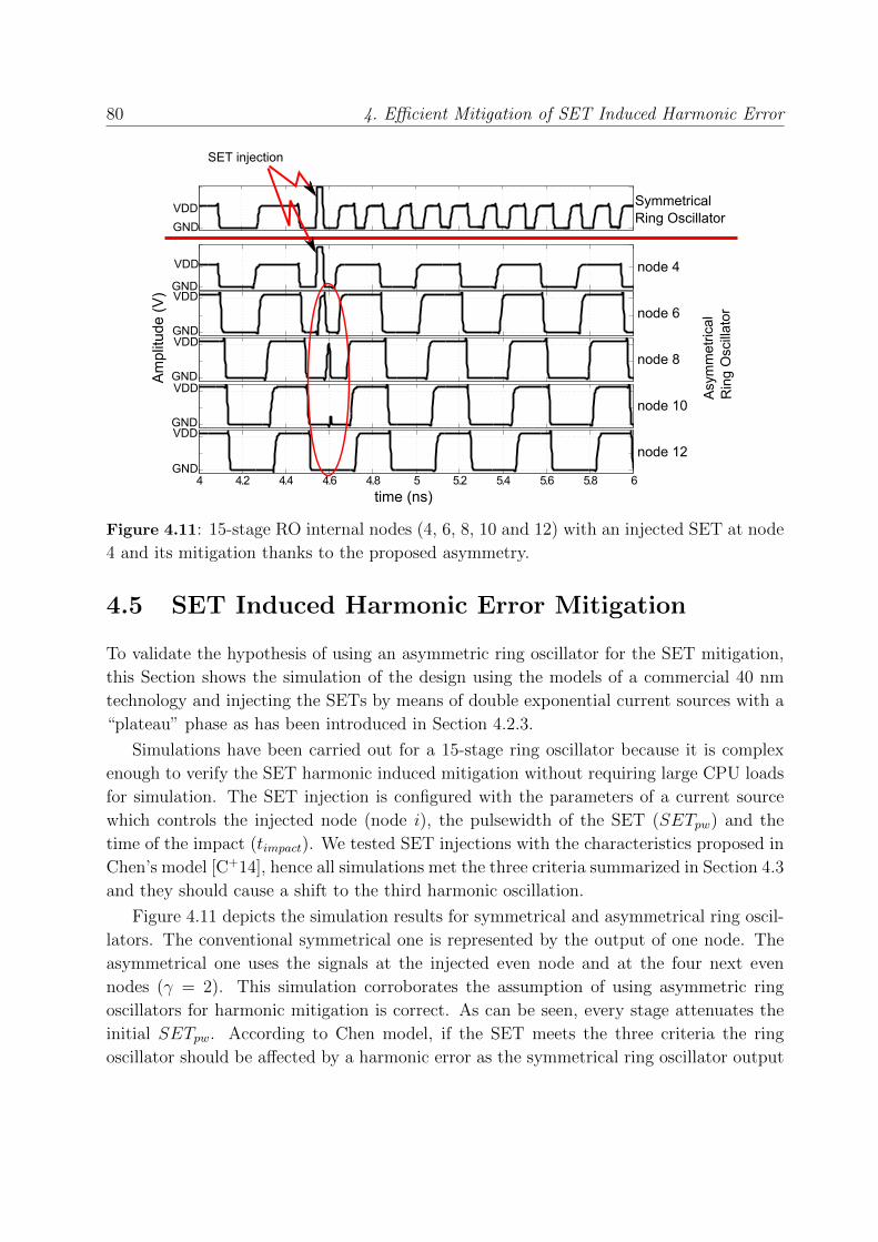
80 4. Efficient Mitigation of SET Induced Harmonic Error
4.2 4.4 4.6 4.8 5 5.2 5.4 5.6 5.8GND
VDD
VDD
4.2 4.4 4.6 4.8 5 5.2 5.4 5.6 5.8GND
VDD
GND
VDD
GND
VDD
GND
VDD
4.2 4.4 4.6 4.8 5 5.2 5.4 5.6 5.8
4.2 4.4 4.6 4.8 5 5.2 5.4 5.6 5.8
4 4.2 4.4 4.6 4.8 5 5.2 5.4 5.6 5.8 6
Am
plitu
deD(
V)
timeD(ns)
nodeD4
nodeD6
nodeD8
nodeD10
nodeD12
SETDinjection
SymmetricalRingDOscillator
Asy
mm
etric
alR
ingD
Osc
illa
tor
VDD
GND
Figure 4.11: 15-stage RO internal nodes (4, 6, 8, 10 and 12) with an injected SET at node
4 and its mitigation thanks to the proposed asymmetry.
4.5 SET Induced Harmonic Error Mitigation
To validate the hypothesis of using an asymmetric ring oscillator for the SET mitigation,
this Section shows the simulation of the design using the models of a commercial 40 nm
technology and injecting the SETs by means of double exponential current sources with a
“plateau” phase as has been introduced in Section 4.2.3.
Simulations have been carried out for a 15-stage ring oscillator because it is complex
enough to verify the SET harmonic induced mitigation without requiring large CPU loads
for simulation. The SET injection is configured with the parameters of a current source
which controls the injected node (node i), the pulsewidth of the SET (SETpw) and the
time of the impact (timpact). We tested SET injections with the characteristics proposed in
Chen’s model [C+14], hence all simulations met the three criteria summarized in Section 4.3
and they should cause a shift to the third harmonic oscillation.
Figure 4.11 depicts the simulation results for symmetrical and asymmetrical ring oscil-
lators. The conventional symmetrical one is represented by the output of one node. The
asymmetrical one uses the signals at the injected even node and at the four next even
nodes (γ = 2). This simulation corroborates the assumption of using asymmetric ring
oscillators for harmonic mitigation is correct. As can be seen, every stage attenuates the
initial SETpw. According to Chen model, if the SET meets the three criteria the ring
oscillator should be affected by a harmonic error as the symmetrical ring oscillator output

4.5. SET Induced Harmonic Error Mitigation 81
NO SET(a)
n0 m0
SET induced
p0
(b)
n1=n0 m1=m0
Symmetrical RO
p1=p0
(c)
n1=n0 m1=m0
Asymmetrical RO
p1=p0
(d)
Figure 4.12: SET propagation within the ring oscillator nodes. Dashed-lines are the edges
induced by a SET.
shown on the top of Figure4.11. In Figure 4.11 the node 12 is not altered by the injection
at node 4, therefore the output node N is also unaffected.
It may seem that the attenuation is because tdmax is longer in our proposal than in
conventional ring oscillators but this is not the real reason, which is depicted in Figure
4.12. When this circuit is working at its fundamental frequency, there is only one node
switching at a time as in Figure 4.12(a). We divided its operation into two modes: first, the
rising edge propagation while node N is low; second, the falling edge while it is high. If the
SET third harmonic appears as described in [C+14], then there are three nodes switching
simultaneously instead of just one according to Figure 4.12(b). n0 is the number of nodes
between the two edges excited by the SET impact, m0 is the number of nodes between the
first node induced by the SET and the edge of the normal behavior and p0 is the number
of nodes between the edge of the normal behavior and the second node induced by the
SET. The three values are defined just at the moment when the particle hits. In ring
oscillators composed by balanced gates, the time of falling and rising edges propagation
is the same, so the edges keep their distance constant a long time as in Fig 4.12(c). n1,
m1 and p1 are the same parameters but a certain time after the ion impact. On the other
hand, our asymmetric design establishes different paths for rising and falling edges with
different time delays (N ∗ tdorise and N ∗ tderise). This difference is shown in Fig 4.12(d), it
lets the fast edges “catch” the slow ones neutralizing the third harmonic excitation.
The proposed ring oscillator has shown the total mitigation of harmonic induced errors,
but there is still a chance of the SET to appear at the ring oscillator output. From Fig-
ure 4.11 we conclude that a SET with a pulsewidth SETpw propagates through a number of
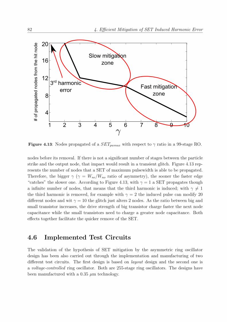
82 4. Efficient Mitigation of SET Induced Harmonic Error
4
8
12
16
20
1 2 3 4 5 6 7 8 9 10
#Fof
Fpro
pag
ated
Fnod
esFfr
om
FtheF
hitFn
ode
3rdFharmonicerror
SlowFmitigationzone
FastFmitigationzone
Figure 4.13: Nodes propagated of a SETpwmax with respect to γ ratio in a 99-stage RO.
nodes before its removal. If there is not a significant number of stages between the particle
strike and the output node, that impact would result in a transient glitch. Figure 4.13 rep-
resents the number of nodes that a SET of maximum pulsewidth is able to be propagated.
Therefore, the bigger γ (γ = Wne/Wno ratio of asymmetry), the sooner the faster edge
“catches” the slower one. According to Figure 4.13, with γ = 1 a SET propagates though
a infinite number of nodes, that means that the third harmonic is induced; with γ 6= 1
the third harmonic is removed, for example with γ = 2 the induced pulse can modify 20
different nodes and wit γ = 10 the glitch just alters 2 nodes. As the ratio between big and
small transistor increases, the drive strength of big transistor charge faster the next node
capacitance while the small transistors need to charge a greater node capacitance. Both
effects together facilitate the quicker remove of the SET.
4.6 Implemented Test Circuits
The validation of the hypothesis of SET mitigation by the asymmetric ring oscillator
design has been also carried out through the implementation and manufacturing of two
different test circuits. The first design is based on layout design and the second one is
a voltage-controlled ring oscillator. Both are 255-stage ring oscillators. The designs have
been manufactured with a 0.35 µm technology.

4.6. Implemented Test Circuits 83
enable
odd nodeeven nodeWpo
Wno
Wpe
Wne
Vdd Vdd
Wpo
Wno
Vdd Vdd
node 1 Wpo
Wno
VddVdd
Wpe
Wne
Wpe
Wne
Figure 4.14: Schematic of the ring oscillator used for SET emulation in electrical valida-
tion.
The injection of controlled SETs in manufactured test circuits is not a simple task as
it is at simulation where a current source with a function defined by the expected type of
SET is defined. In Section 4.2.2, the standard test for SEE has been introduced. However,
all of those test methods require special equipment and are expensive ranging from $1000
per day, to $1000 per hour. To avoid those costs, some previous works has developed an
emulation system such as fault emulation systems with additional boards [EGVFC+12]
or built-in self-test design [LKJ+12]. The first one presents advantages for configurable
platforms like FPGA systems, while the last procedure seems the most suitable for the
case of study of this thesis.
Then for emulating a SET into the manufactured chip we want to force the ring os-
cillator to oscillate at its third harmonic frequency instead of its fundamental. The ring
oscillator loop configuration gives the opportunity of exciting the third harmonic oscillation
just when the enable is triggered following the schematic of Figure 4.14. Additionally, forc-
ing the third harmonic during steady oscillation requires a perfect synchronization to excite
an additional pulse that fulfills the SET harmonic error criteria. This synchronization was
achieved with an auxiliary circuit.
The schematic of Figure 4.14 differs from the other ring oscillators in the number of
enable inputs in the design. Conventional ring oscillators just use one NAND gate to enable
the oscillation. But we use three different NAND gates to start the ring oscillator. This
emulation technique removes the randomness of ion strikes but it deals with the worst
case of third harmonic error induction. The relative positions between them define the
characteristic of the emulated SET:
• The distance between two consecutive NAND gates must be an odd number of ring
oscillator stages. For example, if we consider the first NAND at node 1, then the
second one has to be at an even node, and the third one at an odd node.
• The distance between two consecutive NAND gates must be configured to generate
a SET pulsewidth (tSET ) that fulfills the criteria of Harmonic Vulnerability Window.
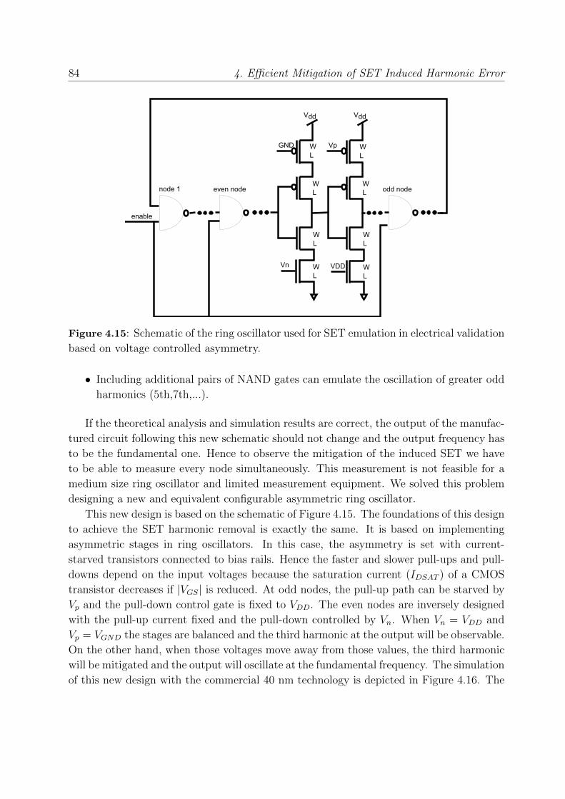
84 4. Efficient Mitigation of SET Induced Harmonic Error
node 1WL
WL
Vdd
GND
WL
WL
Vdd
Vp
enable
odd nodeeven node
WL
WL
Vn VDD
WL
WL
Figure 4.15: Schematic of the ring oscillator used for SET emulation in electrical validation
based on voltage controlled asymmetry.
• Including additional pairs of NAND gates can emulate the oscillation of greater odd
harmonics (5th,7th,...).
If the theoretical analysis and simulation results are correct, the output of the manufac-
tured circuit following this new schematic should not change and the output frequency has
to be the fundamental one. Hence to observe the mitigation of the induced SET we have
to be able to measure every node simultaneously. This measurement is not feasible for a
medium size ring oscillator and limited measurement equipment. We solved this problem
designing a new and equivalent configurable asymmetric ring oscillator.
This new design is based on the schematic of Figure 4.15. The foundations of this design
to achieve the SET harmonic removal is exactly the same. It is based on implementing
asymmetric stages in ring oscillators. In this case, the asymmetry is set with current-
starved transistors connected to bias rails. Hence the faster and slower pull-ups and pull-
downs depend on the input voltages because the saturation current (IDSAT ) of a CMOS
transistor decreases if |VGS| is reduced. At odd nodes, the pull-up path can be starved by
Vp and the pull-down control gate is fixed to VDD. The even nodes are inversely designed
with the pull-up current fixed and the pull-down controlled by Vn. When Vn = VDD and
Vp = VGND the stages are balanced and the third harmonic at the output will be observable.
On the other hand, when those voltages move away from those values, the third harmonic
will be mitigated and the output will oscillate at the fundamental frequency. The simulation
of this new design with the commercial 40 nm technology is depicted in Figure 4.16. The

4.7. Electrical Validation 85
0
0.4
0.8
1.2
0 1 2 3 4 5 6 7 8 9 10
Vpo=oGNDoandoVn=VDD Vpo=GNDooroVn=VDDoenableoRO
Am
plitu
deo(
V)
timeo(ns)
Figure 4.16: Output waveform of the third harmonic removal in the simulation of the
voltage-controlled test circuit validation.
third harmonic disappearance is clearly observable when the voltages are changed.
Finally the device under test (DUT) has two analog inputs (Vn and Vp), one digital
input (enable) and three digital outputs (ROLayout, ROV C1 and ROV C2). ROLayout
is the output of the layout solution, ROV C1 is the output of the final node of the voltage-
controlled test circuit and ROV C2 is an intermediate node (node 126). The manufactured
layout is shown in Figure 4.17. The three outputs are different to the NAND gate outputs
because from Figure 4.13 these nodes will always experience a glitch.
The Layout-based design was implemented with γ = 2. The technology design rules
constrain the minimum area of the ring oscillator design. With this value of γ the area is
the same as the minimum area (γ = 1 and minimum transistors) ring oscillator therefore
there is no area overhead. For larger values of γ the area overhead increases, for instance
with γ = 8 the area is twice.
4.7 Electrical Validation
The electrical validation of the manufactured designs consists in emulating the SET injec-
tions and analyzing the observable signals at the outputs of the two different test circuits.
The layout implementation has been designed to mitigate SETs in any scenario. The
voltage-controlled solution allows to configure the asymmetry of the design in order to
define the degree of the needed asymmetry to remove the third harmonic induced error.

86 4. Efficient Mitigation of SET Induced Harmonic Error
350 m
300
m Layout-based
Voltage-Controlled
SET emulation NAND gates
enable
output
Vn
Vp
output
intermediateoutput
Figure 4.17: Layout of the two different manufactured test circuits with their inputs and
outputs. (top) layout-based. (bottom) voltage-controlled.
4.7.1 Test Set Up
Figure 4.18 illustrates the workbench used for the electrical test. The measurements were
carried out with this equipment:
• A custom test-board to allocate the DUT. It was designed to be versatile for different
types of tests.
• A custom bread-board to route the I/O signals of the DUT with relays and adaptive
stages.
• A Virtex5 ML505 Xilinx FPGA development board to generate the input signals of
the DUT and to perform the configuration of the bread-board.
• An Agilent MSO9051 oscilloscope to capture the output signals of the DUT.
• A PC to control the test through the communication interfaces: Ethernet and USB.
• An Ethernet switch that connects the equipment.

4.7. Electrical Validation 87
(a)
(b)
DUT
Oscilloscope
FPGAhboard
Bread-board
Test-board
PChInterface
Osc
illos
cope
SwitchEth
Core
Figure 4.18: Set Up used for the validation tests of our new ring oscillator design.
4.7.2 Experimental Results
The test plan we carried out considered different scenarios. All the measurements were
made at two different stages: first, at the oscillation start; and, second, at a steady oscil-
lation 500 ms after the enable activation. In addition each measurement was repeated 20
times to remove any spurious situation or anomalous signal. Then we measured the two
different block outputs. The layout-based ring oscillator was made following the explained
procedure. The voltage-controlled ring oscillator required a previous plan of the input volt-
ages. We measured 121 different inputs. We divided this voltage into 11 intervals and we
tested all combinations for Vp and Vn.
The main situations that took place during all the tests are collected in Figure 4.19.
Figure 4.19 (a) is the result of the layout-based ring oscillator. As was expected, the result
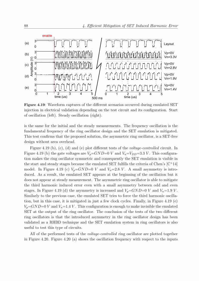
88 4. Efficient Mitigation of SET Induced Harmonic Error
500 ms
Layout
Vp=0VVn=3.3V
Vp=0VVn=2.8V
Vp=0VVn=1.9V
Vp=0VVn=1.4V
Am
plitu
de (
V)
3
0
3
0
3
0
3
0
3
00 1 2 3 4 5
time (us)0 1 2 3 4 5
time (us)
enable
(a)
(b)
(c)
(d)
(e)
Figure 4.19: Waveform captures of the different scenarios occurred during emulated SET
injection in electrical validation depending on the test circuit and its configuration. Start
of oscillation (left). Steady oscillation (right).
is the same for the initial and the steady measurements. The frequency oscillation is the
fundamental frequency of the ring oscillator design and the SET emulation is mitigated.
This test confirms that the proposed solution, the asymmetric ring oscillator, is a SET-free
design without area overhead.
Figure 4.19 (b), (c), (d) and (e) plot different tests of the voltage-controlled circuit. In
Figure 4.19 (b) the gate voltages are Vp=GND=0 V and Vn=VDD=3.3 V . This configura-
tion makes the ring oscillator symmetric and consequently the SET emulation is visible in
the start and steady stages because the emulated SET fulfills the criteria of Chen’s [C+14]
model. In Figure 4.19 (c) Vp=GND=0 V and Vn=2.8 V . A small asymmetry is intro-
duced. As a result, the emulated SET appears at the beginning of the oscillation but it
does not appear at steady measurement. The asymmetric ring oscillator is able to mitigate
the third harmonic induced error even with a small asymmetry between odd and even
stages. In Figure 4.19 (d) the asymmetry is increased and Vp=GND=0 V and Vn=1.9 V .
Similarly to the previous case, the emulated SET tries to force the third harmonic oscilla-
tion, but in this case, it is mitigated in just a few clock cycles. Finally, in Figure 4.19 (e)
Vp=GND=0 V and Vn=1.4 V . This configuration is enough to make invisible the emulated
SET at the output of the ring oscillator. The conclusion of the tests of the two different
ring oscillators is that the introduced asymmetry in the ring oscillator design has been
validated as a RHBD technique and the SET emulation system in ring oscillators is also
useful to test this type of circuits.
All of the performed tests of the voltage-controlled ring oscillator are plotted together
in Figure 4.20. Figure 4.20 (a) shows the oscillation frequency with respect to the inputs
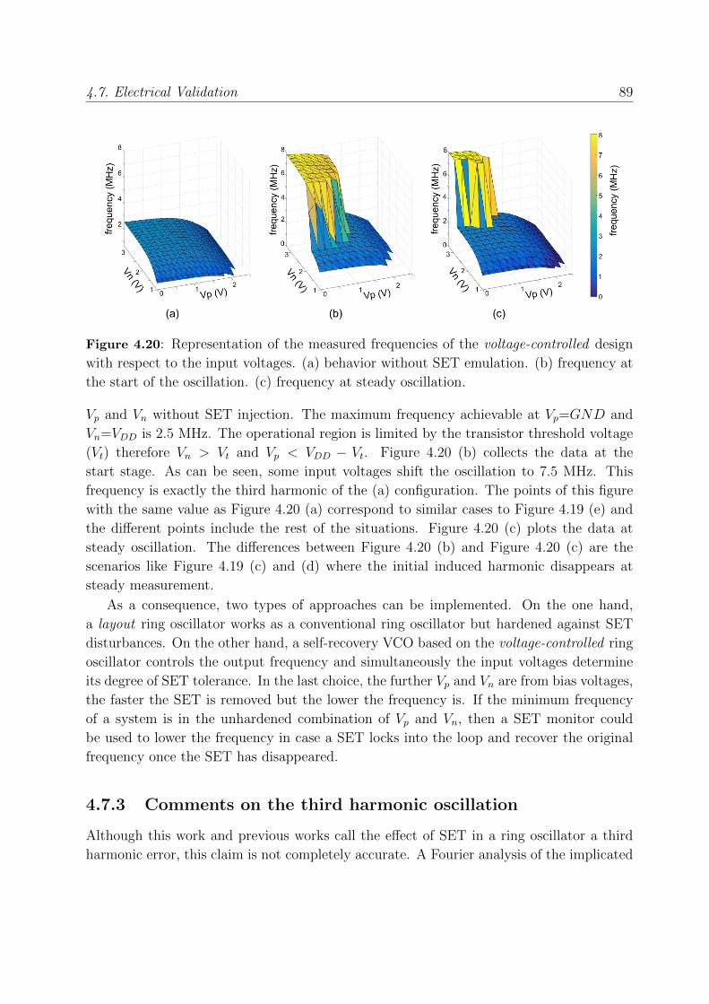
4.7. Electrical Validation 89
Figure 4.20: Representation of the measured frequencies of the voltage-controlled design
with respect to the input voltages. (a) behavior without SET emulation. (b) frequency at
the start of the oscillation. (c) frequency at steady oscillation.
Vp and Vn without SET injection. The maximum frequency achievable at Vp=GND and
Vn=VDD is 2.5 MHz. The operational region is limited by the transistor threshold voltage
(Vt) therefore Vn > Vt and Vp < VDD − Vt. Figure 4.20 (b) collects the data at the
start stage. As can be seen, some input voltages shift the oscillation to 7.5 MHz. This
frequency is exactly the third harmonic of the (a) configuration. The points of this figure
with the same value as Figure 4.20 (a) correspond to similar cases to Figure 4.19 (e) and
the different points include the rest of the situations. Figure 4.20 (c) plots the data at
steady oscillation. The differences between Figure 4.20 (b) and Figure 4.20 (c) are the
scenarios like Figure 4.19 (c) and (d) where the initial induced harmonic disappears at
steady measurement.
As a consequence, two types of approaches can be implemented. On the one hand,
a layout ring oscillator works as a conventional ring oscillator but hardened against SET
disturbances. On the other hand, a self-recovery VCO based on the voltage-controlled ring
oscillator controls the output frequency and simultaneously the input voltages determine
its degree of SET tolerance. In the last choice, the further Vp and Vn are from bias voltages,
the faster the SET is removed but the lower the frequency is. If the minimum frequency
of a system is in the unhardened combination of Vp and Vn, then a SET monitor could
be used to lower the frequency in case a SET locks into the loop and recover the original
frequency once the SET has disappeared.
4.7.3 Comments on the third harmonic oscillation
Although this work and previous works call the effect of SET in a ring oscillator a third
harmonic error, this claim is not completely accurate. A Fourier analysis of the implicated
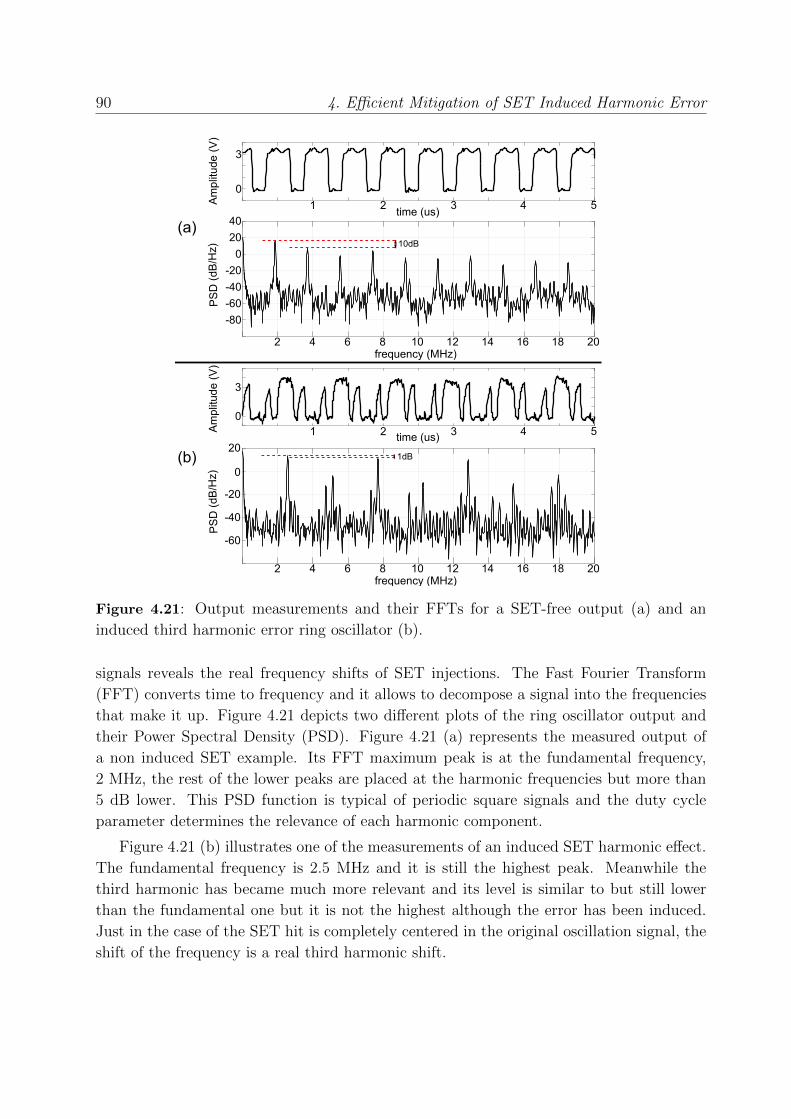
90 4. Efficient Mitigation of SET Induced Harmonic Error
frequencyi(MHz)2 4 6 8 10 12 14 16 18 20
frequencyi(MHz)2 4 6 8 10 12 14 16 18 20
40
20
0
-20
-40
-60
-80
20
0
-20
-40
-60
PS
Di(
dB/H
z)A
mpl
itude
i(V
)A
mpl
itude
i(V
)
3
0
3
0
timei(us)
timei(us)1 2 3 4 5
1 2 3 4 5
(a)
(b) 1dB
PS
Di(
dB/H
z) 10dB
Figure 4.21: Output measurements and their FFTs for a SET-free output (a) and an
induced third harmonic error ring oscillator (b).
signals reveals the real frequency shifts of SET injections. The Fast Fourier Transform
(FFT) converts time to frequency and it allows to decompose a signal into the frequencies
that make it up. Figure 4.21 depicts two different plots of the ring oscillator output and
their Power Spectral Density (PSD). Figure 4.21 (a) represents the measured output of
a non induced SET example. Its FFT maximum peak is at the fundamental frequency,
2 MHz, the rest of the lower peaks are placed at the harmonic frequencies but more than
5 dB lower. This PSD function is typical of periodic square signals and the duty cycle
parameter determines the relevance of each harmonic component.
Figure 4.21 (b) illustrates one of the measurements of an induced SET harmonic effect.
The fundamental frequency is 2.5 MHz and it is still the highest peak. Meanwhile the
third harmonic has became much more relevant and its level is similar to but still lower
than the fundamental one but it is not the highest although the error has been induced.
Just in the case of the SET hit is completely centered in the original oscillation signal, the
shift of the frequency is a real third harmonic shift.

4.8. Conclusions 91
4.8 Conclusions
This chapter has addressed the harmonic induced error, presented in [C+14], caused by
SETs in ring oscillators. We have proposed a new ring oscillator design that fully tolerates
this error. Our solution supposes a negligible area overhead compared to the common ring
oscillator implementation. This new design differs from conventional ring oscillators in the
utilization of non-equal and unbalanced inverters for their stages. Moreover, odd and even
nodes are designed asymmetrically. It means that odd nodes use faster pull up networks
while even nodes use faster pull downs. This modification provides the ability of designing
a configurable duty cycle output depending on the implemented degree of asymmetry with
negligible area overhead.
We have introduced the approach by theoretical analysis, we have validated it with
simulations and we have manufactured two approaches based on the same foundations to
perform an electrical characterization. The first approach fixes the asymmetry of the ring
oscillator with the size of transistors. The second design uses two different input voltages
to dynamically control the unbalanced stages. We have also designed a methodology for
the emulation of SET injection in ring oscillators to avoid the high costs of a SET radiation
campaign. Both approaches have contributed to the validation of the hypothesis.
Our solution contributes to improve the tolerance of ring oscillator based applications
to radiation effects and as a consequence to increase the reliability of circuits that use them.
For example, ring oscillators are used as simple clock generators for many test circuits in
radiation characterizations, therefore a harmonic error produced by an induced transient
will mislead about the real characteristics of the tested circuits.
At the same time, the work presented in this chapter has generated a new design of
ring oscillators, it also opens a new perspective into ring oscillator utilization. So far, ring
oscillators have been used to generate clock signals with 50% duty cycle. But, as the next
chapter will explain, the use of duty cycle can open the door to new unexplored possibilities
of these circuits.
4.9 Related Publications
• J. Agustin, M. L. Lopez-Vallejo, C. G. Soriano, P. Cholbi, L. W. Massengill and Y.
P. Chen, ”Efficient Mitigation of SET Induced Harmonic Errors in Ring Oscillators,”
in NSREC 2015, Boston, Jul. 2015.
• J. Agustin, M. L. Lopez-Vallejo, C. G. Soriano, P. Cholbi, L. W. Massengill and Y.
P. Chen, ”Efficient Mitigation of SET Induced Harmonic Errors in Ring Oscillators,”
in IEEE Transactions on Nuclear Science, vol. 62, no. 6, pp. 3049-3056, Dec. 2015.
doi: 10.1109/TNS.2015.2496169


Chapter 5
Analytical Model of the DutyCycle in Ring Oscillators

Chapter 5
Analytical Model of the Duty Cycle in RingOscillators
5.1 Introduction
In Chapter 4 we have introduced a solution to mitigate SETs that implies a new approach
to the design of ring oscillators. This approach is based on implementing a ring oscillator
with unbalanced gates. As has been validated in the previous chapter, using this technique
allows to fully configure the duty cycle of ring oscillators.
Previously, in Chapter 2, the relevancy of ring oscillators in electronics has been shown.
Some applications are listed in that chapter (DLLs, PLLs, PVT sensors, TDCs, etc.), but
all of those applications take advantage of the ring oscillator output frequency and its
shift for different stimulus variations. Moreover, systems that require clock signals with
configurable duty cycles or different from 50% leave this task to complementary blocks
such as in [AG11,KHZS07,VGB07,AHM03]. Then, the implementation of a ring oscillator
design with parameterizable duty cycle saves resources and, at the same time, supposes a
step further in the utilization of ring oscillator features. In [VAFK14] a similar approach to
this problem is presented, but it is just a simple implementation using just one node of ring
oscillators while we present in this chapter a fully analytical model for the configuration of
duty cycle in every node of ring oscillators. Our model is derived from the generalization
of the implemented ring oscillator for SET mitigation.
The development of this task has to begin with the analytical study of the parameters
that define the output duty cycle. This analysis leads to two different parameters, the
aspect ratio of transistors and the bias voltage. Therefore, this chapter develops two
different techniques with negligible or low area overhead to achieve the variation of the
output duty cycle. On the one hand, a hard implementation that uses an individual
transistor sizing methodology. This first strategy is defined at the layout level making
each implementation unique and invariable after its fabrication. On the other hand, the
soft approach uses different bias voltages for each ring oscillator stage. This strategy
allows a dynamic configuration of the output duty cycles during its operation time. Both
models confirm analytically the circuits used in Chapter 4 —layout and voltage-controlled.
We use different terms to refer the generalized models hard and soft from the particular

5.2. Model Analysis 95
implementations layout and voltage-controlled.
Our proposal is modeled, characterized and validated in this chapter considering dif-
ferent configurations, process variations and phase noise. The results of this study set this
new design approach as a potential block for many different electronic systems to improve
their actual performance. For instance, in the next chapter will take advantage of this
formulation to build a particular application, a PUF, that uses the output duty cycle of
ring oscillators to improve the robustness of conventional ring oscillator based PUFs.
This chapter is organized as follows: First in Section 5.2 an analysis of CMOS ring
oscillators is presented, which seeks to establish the analytical basis in order to understand
this electronic circuit and the potential of its duty cycle variation. Using the conclusions
of this analysis, in Section 5.3 the two models of duty cycle variation —hard and soft— are
developed. These models are validated and characterized through simulation with a 40 nm
commercial technology in Section 5.4. In Section 5.5 we study the jitter and phase noise
of the ring oscillator depending on the duty cycle configuration. Finally the conclusions of
the main contributions of this chapter are drawn in Section 5.7.
5.2 Model Analysis
The final goal of this analysis is to implement a ring oscillator that provides outputs with
configurable duty cycles. Achieving this target makes necessary firstly to understand how
a ring oscillator works and how it oscillates. Therefore we explain the foundations of this
circuit in this Section 5.2. After that description, design variables that affect the ring
oscillator output properties will be analyzed to support which parameters are suitable to
control the oscillation duty cycle.
We only take into consideration single-ended CMOS ring oscillators whose delay ele-
ments are made of simple inverter gates. In spite of this limitation, the conclusions can be
directly extrapolated to the rest of ring oscillator topologies.
Single-ended ring oscillators are composed of an odd chain inverter stages whose last
output is fed back to its first input gate. The basis of the oscillation is the instability of
nodes thanks to the odd number of delay stages. This property makes nodes fluctuate with
a period proportional to the addition of the propagation delay of each individual inverter.
Therefore, the first step to understand the behavior of the complete ring oscillator is
exploring how the design of the simplest component —individual CMOS inverter gates in
this case— impacts on the output frequency and duty cycle.
5.2.1 CMOS Inverter
We follow the long-channel model of MOS transistors [WH11] to analyze the CMOS inverter
delay. According to this model, the source-drain current of an individual transistor is ruled

96 5. Analytical Model of the Duty Cycle in Ring Oscillators
by the equation:
Ids =Qch
L/v= µCox
W
L(Vgs − Vt − Vds/2)Vds (5.1)
where Qch is the charge inside the channel, L is the channel length, v is the average velocity
of carriers, µ is the electron/hole mobility constant, Cox is the capacitance per unit area
of gate oxide, W is the channel width, Vt is the transistor threshold voltage, Vgs is the
gate-source voltage and Vds is the drain-source voltage.
(5.1) is traditionally divided into three1 different regions depending on the input volt-
ages:
Ids =
0 Vgs < Vt Off
β(Vgs − Vt − Vds2 )Vds Vds < VDSAT Linear
β2 (Vgs − V t)2 Vds > VDSAT Saturation
(5.2)
where VDSAT splits ohmic mode from saturation mode and β is defined by β = µCoxW/L.
To set the propagation delay of an inverter the load capacitance must be known. Since
the inverters of a ring oscillator are disposed in a loop configuration, the load capacitance
of each inverter is highly influenced by the gate capacitance of the next inverter. Thus
another important parameter to determine the propagation delay of CMOS inverters within
ring oscillators is their gate capacitance which is defined as:
Cg = Cox(Wn +Wp)L (5.3)
It is not our aim to develop the most accurate model of ring oscillators but modeling its
behavior as easy as possible to outline the designing factors that affect its performance and
a way to vary it. Therefore to simplify the chain of inverters we make these assumptions:
First, each transistor is replaced by an equivalent current source characterized by its source-
drain current; Second, the load capacitance of a node is equal to the gate capacitance
of the next stage —we consider negligible for this first approximation the rest of node
capacitances. Hence if pMOS transistors charge a Cl and nMOS transistors discharge it,
then the expression that rules the discharge of a node by an nMOS transistor can be defined
as:
CldVdsdt
= −Idsn (5.4)
Taking into account the different operational modes in (5.2) in which transistors are
not cutoff and using VDD instead of Vgs, (5.4) can be split into these two zones:
1Velocity saturation and other secondary effects are not considered in this model, but their consideration
does not affect the conclusion of our model, as will be shown by the experiments we have carried out.
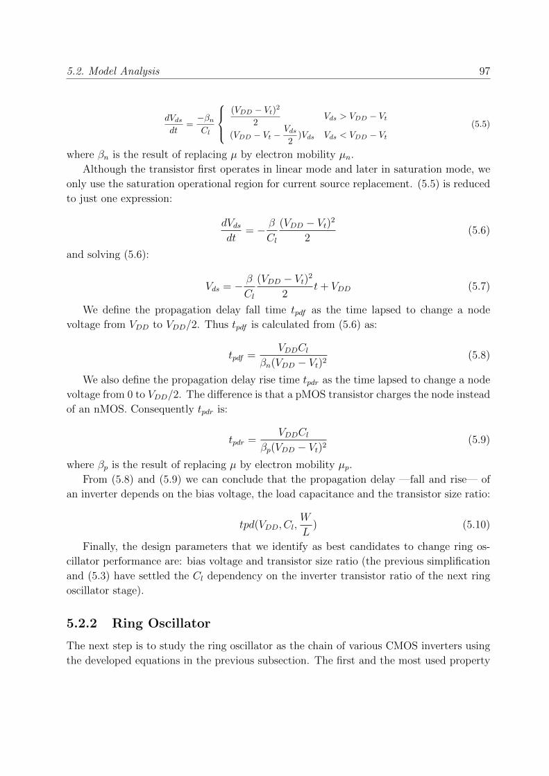
5.2. Model Analysis 97
dVdsdt
=−βnCl
(VDD − Vt)2
2Vds > VDD − Vt
(VDD − Vt −Vds2
)Vds Vds < VDD − Vt(5.5)
where βn is the result of replacing µ by electron mobility µn.
Although the transistor first operates in linear mode and later in saturation mode, we
only use the saturation operational region for current source replacement. (5.5) is reduced
to just one expression:
dVdsdt
= − β
Cl
(VDD − Vt)2
2(5.6)
and solving (5.6):
Vds = − β
Cl
(VDD − Vt)2
2t+ VDD (5.7)
We define the propagation delay fall time tpdf as the time lapsed to change a node
voltage from VDD to VDD/2. Thus tpdf is calculated from (5.6) as:
tpdf =VDDCl
βn(VDD − Vt)2(5.8)
We also define the propagation delay rise time tpdr as the time lapsed to change a node
voltage from 0 to VDD/2. The difference is that a pMOS transistor charges the node instead
of an nMOS. Consequently tpdr is:
tpdr =VDDCl
βp(VDD − Vt)2(5.9)
where βp is the result of replacing µ by electron mobility µp.
From (5.8) and (5.9) we can conclude that the propagation delay —fall and rise— of
an inverter depends on the bias voltage, the load capacitance and the transistor size ratio:
tpd(VDD, Cl,W
L) (5.10)
Finally, the design parameters that we identify as best candidates to change ring os-
cillator performance are: bias voltage and transistor size ratio (the previous simplification
and (5.3) have settled the Cl dependency on the inverter transistor ratio of the next ring
oscillator stage).
5.2.2 Ring Oscillator
The next step is to study the ring oscillator as the chain of various CMOS inverters using
the developed equations in the previous subsection. The first and the most used property

98 5. Analytical Model of the Duty Cycle in Ring Oscillators
node 1 node i node N
Wp1Lp1
Wn1Ln1
WpiLpi
WniLni
WpNLpN
WnNLnN
Vdd1 Vddi VddN
C1 Ci CN
Figure 5.1: Ring Oscillator notation. W (transistor width), L (transistor channel length),
Ci (node i capacitance), and Vddi (bias voltage of inverter i).
of a ring oscillator is the output frequency. The ring oscillator period T can be estimated
as the addition of all inverter propagation delays:
T = 2 ∗∑
tpdi (5.11)
But this work is mainly focused on controlling the duty cycle of every stage output
instead of the output frequency. Thus, the period can be divided into thigh —the output
is higher than VDD/2— and tlow —the output is lower than VDD/2. Therefore (5.11) is
redefined as:
T = tlow + thigh (5.12)
A more specific analysis of the terms of this partitioning requires a new division for
each individual node. Figure 5.1 sets the notation we follow to differentiate nodes within a
ring oscillator. The output of a ring oscillator is usually just one node and its frequency is
a general feature because all internal nodes oscillate with the same period. But our study
assumes N potential outputs —one per node— that are dependent but different. So if T
refers to the period of node N, then tlow and thigh in (5.12) can be defined, generalizing the
5-stage ring oscillator internal nodes of Figure 5.2, by:
tlowN = tpdrN +
N−12∑1
(tpdf2i + tpdr2i−1) (5.13)
thighN = tpdfN +
N−12∑1
(tpdf2i−1 + tpdr2i) (5.14)

5.2. Model Analysis 99
0
0.5
1
V
0
0.5
1V
0
0.5
1
V
0
0.5
1
V
1 1.5 2 2.5 3 3.5 4 4.5 50
0.5
1
time (ns)
V
node 1
node 2
node 3
node 4
node 5
tpdr1
tpdf2
tpdr3
tpdf4
tpdr5 tpdf
5
tpdr4
tpdf3
tpdr2
tpdf1
Figure 5.2: Internal nodes of a balanced 5-stage ring oscillator and the times in which the
period, T is divided.
The particularization of the dependency in (5.10) for the ring oscillator nodes results
in:
tpdfi(VDDi+1, Cl(i+1)
, (Wni
Lni)) =
= tpdfi(VDDi+1, (Wn(i+1)
Ln(i+1)
), (Wp(i+1)
Lp(i+1)
), (Wni
Lni))
(5.15)
tpdri(VDDi , Cl(i+1), (Wpi
Lpi)) =
= tpdri(VDDi , (Wn(i+1)
Ln(i+1)
), (Wp(i+1)
Lp(i+1)
), (Wpi
Lpi))
(5.16)
Putting all together, the variables that can modify the characteristics of the output
signal and make each node signal different from the others are the aspect ratio design of
every single MOS transistor and the bias voltage of inverters.
The duty cycle of a digital signal is defined as the ratio between thigh and its period
T . Traditional ring oscillators do not consider this parameter because it is supposed to
be 50%. However we can infer from (5.12)-(5.16) that this assumption can be modified.
Generally, the duty cycle of the signal at node i in a ring oscillator is defined as:
di =thighiT
(5.17)
All ring oscillator designs make use of inverters that are exactly the same, then all
tpdri and tpdfi are equal and the duty cycle referred to node N is determined from

100 5. Analytical Model of the Duty Cycle in Ring Oscillators
(5.13), (5.14) and (5.17) by:
dN =N+1
2tpdr + N−1
2tpdf
N(tpdr + tpdf )=
1
2+
tpdr − tpdf2(tpdr + tpdf )
(5.18)
In (5.18) the duty cycle of the ring oscillator output is 50% when the inverters are
balanced (tpdr = tpdf ), otherwise the duty cycle slightly varies from this value.
5.3 Duty Cycle Configuration Models
The conclusion of Section 5.2 is that the duty cycle of the ring oscillator nodes can be
modified by controlling VDD and the transistor aspect ratios. For this reason we have
developed two different methods to vary the duty cycle of each node: a hard method based
on layout design, and a soft one founded on bias voltage variation. In our models we define
the duty cycle of odd nodes as the ratio thigh/T and the duty cycle of even nodes as the
ratio tlow/T to re-invert the signal and normalize its value.
5.3.1 Hard duty cycle configuration
Our first proposal is based on studying the duty cycle at every node for general Wi/Liimplementations. For all transistors Li is equal to the minimum gate length L imposed by
the technology rules. All inverter stages are also biased at the same voltage VDD. (5.13)
and (5.14) are referred to the last node N , but those equations can be redefined for a general
node i. To shorten the notation, we declare the function ΓN(x) = [mod(x−1, N)+1] where
mod(x,N) is the remainder of the division x/N. Thus thigh and tlow referred to node i are:
thighi = tpdfi +
j=i+N−32∑
j=i
(tpdfΓN (2j+1) + tpdrΓN (2j)) (5.19)
tlowi = tpdri +
j=i+N−32∑
j=i
(tpdrΓN (2j+1) + tpdfΓN (2j)) (5.20)
If we bring the definition of β, (5.3) and (5.8) together, then we can define tpdfi for each
inverter with respect to the transistor widths Wi. This definition remains as:
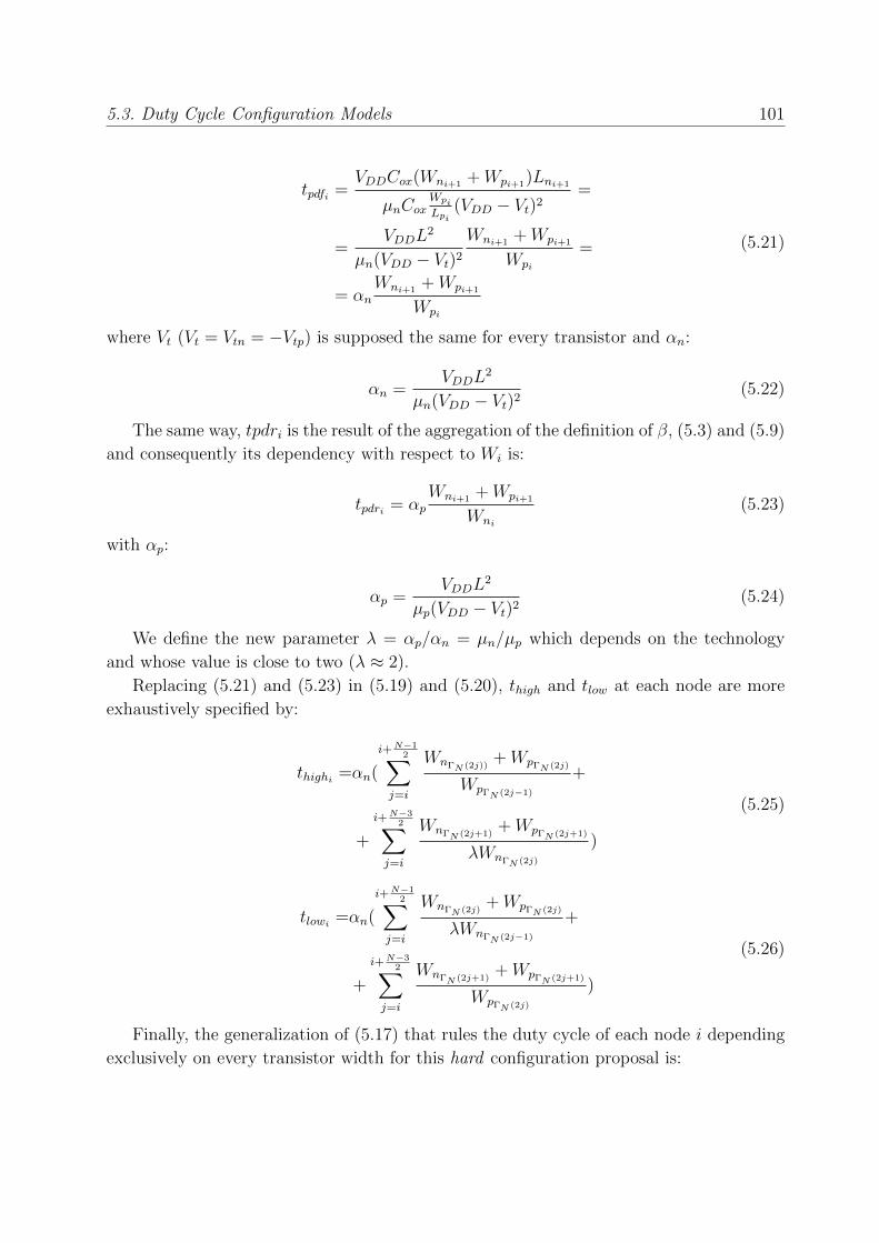
5.3. Duty Cycle Configuration Models 101
tpdfi =VDDCox(Wni+1
+Wpi+1)Lni+1
µnCoxWpi
Lpi(VDD − Vt)2
=
=VDDL
2
µn(VDD − Vt)2
Wni+1+Wpi+1
Wpi
=
= αnWni+1
+Wpi+1
Wpi
(5.21)
where Vt (Vt = Vtn = −Vtp) is supposed the same for every transistor and αn:
αn =VDDL
2
µn(VDD − Vt)2(5.22)
The same way, tpdri is the result of the aggregation of the definition of β, (5.3) and (5.9)
and consequently its dependency with respect to Wi is:
tpdri = αpWni+1
+Wpi+1
Wni
(5.23)
with αp:
αp =VDDL
2
µp(VDD − Vt)2(5.24)
We define the new parameter λ = αp/αn = µn/µp which depends on the technology
and whose value is close to two (λ ≈ 2).
Replacing (5.21) and (5.23) in (5.19) and (5.20), thigh and tlow at each node are more
exhaustively specified by:
thighi =αn(
i+N−12∑
j=i
WnΓN (2j))+WpΓN (2j)
WpΓN (2j−1)
+
+
i+N−32∑
j=i
WnΓN (2j+1)+WpΓN (2j+1)
λWnΓN (2j)
)
(5.25)
tlowi =αn(
i+N−12∑
j=i
WnΓN (2j)+WpΓN (2j)
λWnΓN (2j−1)
+
+
i+N−32∑
j=i
WnΓN (2j+1)+WpΓN (2j+1)
WpΓN (2j)
)
(5.26)
Finally, the generalization of (5.17) that rules the duty cycle of each node i depending
exclusively on every transistor width for this hard configuration proposal is:

102 5. Analytical Model of the Duty Cycle in Ring Oscillators
di =
∑i+N−12
j=i
WnΓN (2j)+WpΓN (2j)
WpΓN (2j−1)+∑N
j=1(WnΓN (j+1)
+WpΓN (j+1)
WpΓN (j)+
WnΓN (j+1)+WpΓN (j+1)
λWnΓN (j))+
+
∑i+N−32
j=i
WnΓN (2j+1)+WpΓN (2j+1)
λWnΓN (2j)∑Nj=1(
WnΓN (j+1)+WpΓN (j+1)
WpΓN (j)+
WnΓN (j+1)+WpΓN (j+1)
λWnΓN (j))
(5.27)
(5.27) explains any case for different Wi distributions in ring oscillators. But to un-
derstand how it works and what is the behavior of internal nodes under this expression
we present some particular Wi patterns. The first example represents the traditional im-
plementation of a ring oscillator, the ratio between pMOS and nMOS transistors is fixed
(γ = Wp/Wn) then the duty cycle expression is:
di =(N+1
2)(γ+1
γ) + (N−1
2)(γ+1
λ)
N(γ+1γ
+ γ+1λ
)=
=1
2+
λ+ (λ− 1)γ − γ2
2N(λ+ (λ+ 1)γ + γ2)
(5.28)
At first sight, the duty cycle does not depend on i so it is the same for every node
within the ring oscillator. (5.28) should agree with the common assumption that the duty
cycle of a ring oscillator is 50%. This hypothesis is fulfilled in two different cases. First,
if γ = λ what solves the second degree equation (λ + (λ − 1)γ − γ2), then the inverters
are balanced (tpdr = tpdf ) and (5.18) and (5.28) match the solution. Second, if N tends to
infinity. λ is fixed by the technology and γ is fixed by the design then:
limN→∞
di =1
2+
κ
2N=
1
2(5.29)
where κ is a constant equal to:
κ =λ+ (λ− 1)γ − γ2
λ+ (λ+ 1)γ + γ2(5.30)
So if N tends to infinity, then the duty cycle of every node tends to 50%.
The second example that helps to understand how the duty cycle can be modified
according to (5.27) follows the schematic depicted in Figure 5.3. In this case the inverters
are divided into odd and even gates. Odd gates have a strong pMOS transistor and a
weak nMOS transistor. And even nodes follow the opposite distribution —strong nMOS
and weak pMOS. If the relationships set between the different transistor widths are Wpo =
Wne = ϕWpe = ϕWno to remove some degrees of freedom, the duty cycle of each node with
these assumptions is approximately:

5.3. Duty Cycle Configuration Models 103
WpoL
WnoL
WpeL
WneL
WpoL
WnoL
Vdd Vdd Vdd
WpoL
WnoL
WpeL
WneL
Vdd Vdd
Co Co CoCe Cenode 1 node 2 node i node i+1 node N
Figure 5.3: Ring Oscillator with asymmetric odd and even nodes (smaller transistors
means narrower channel).
di =(N−i2 )[(ϕ+ 1) + (ϕ+1
λ )] + ( i2)[(ϕ+1ϕ ) + (ϕ+1
λϕ )]
(N+12 )[(ϕ+1
ϕ ) + (ϕ+ 1) + (ϕ+1λϕ ) + (ϕ+1
λ )]=
=ϕN + i(1− ϕ)
(N + 1)(ϕ+ 1)
(5.31)
In this case, (5.31) shows a dependency on i, therefore the duty cycle is different at
different nodes. Besides the duty cycle variation, the schematic of Figure 5.3 produces a
linear duty cycle distribution along the ring oscillator and the slope of this distribution
depends on the ϕ ratio. If ϕ = 1 —all transistor widths are the same—, (5.31) gives a
constant duty cycle for all nodes with a value that tends to 50% as expected from the
previous example (ϕ = 1 ⇒ [Wpo = Wne = Wpe = Wno] and γ = 1 ⇒ [Wp = Wn]).
Moreover, at the central node the duty cycle always tends to 50% independently of the
rest of parameters defined in this example.
The two previous particularizations of the hard model allow a direct simplification
of (5.27), but next examples are plotted directly replacing transistor widths in (5.27).
Figure 5.4 represents four width distributions for four different theoretical examples. These
examples have been calculated for a 51-stage ring oscillator. The K-ratio distribution
follows the schematic of Figure 5.3 with ϕ = 3. The Linear distribution is similar to the
K-ratio but ϕ value is not constant, it follows a linear function with ϕ(1) = ϕ0 = 10
and ϕ(N) = ϕ(51) = 1/ϕ0 = 1/10, and the minimum width is not constant neither with
a linear function with Wpo(1) = W0 and Wpo(N) = Wpo(51) = ϕ0W0. The Increasing
distribution sets the relationships Wpo = Wno = ϕWpe = ϕWne with ϕ and Wpo changing
as in Linear distribution. The Triangle distribution is the result of concatenating two
linear distributions, the first increasing and the second one decreasing with ϕ(1) = ϕ0 = 5,
ϕ((N + 1)/2) = ϕ(26) = 1/ϕ0 = 1/5, ϕ(N) = ϕ(51) = ϕ0 = 5 and Wpo(1) = W0,
Wpo((N + 1))/2) = Wpo(26) = ϕ0W0, Wpo(N) = Wpo(51) = W0. Figure 5.5 depicts the
resulting duty cycle when applying these distributions to (5.27). K-ratio distribution
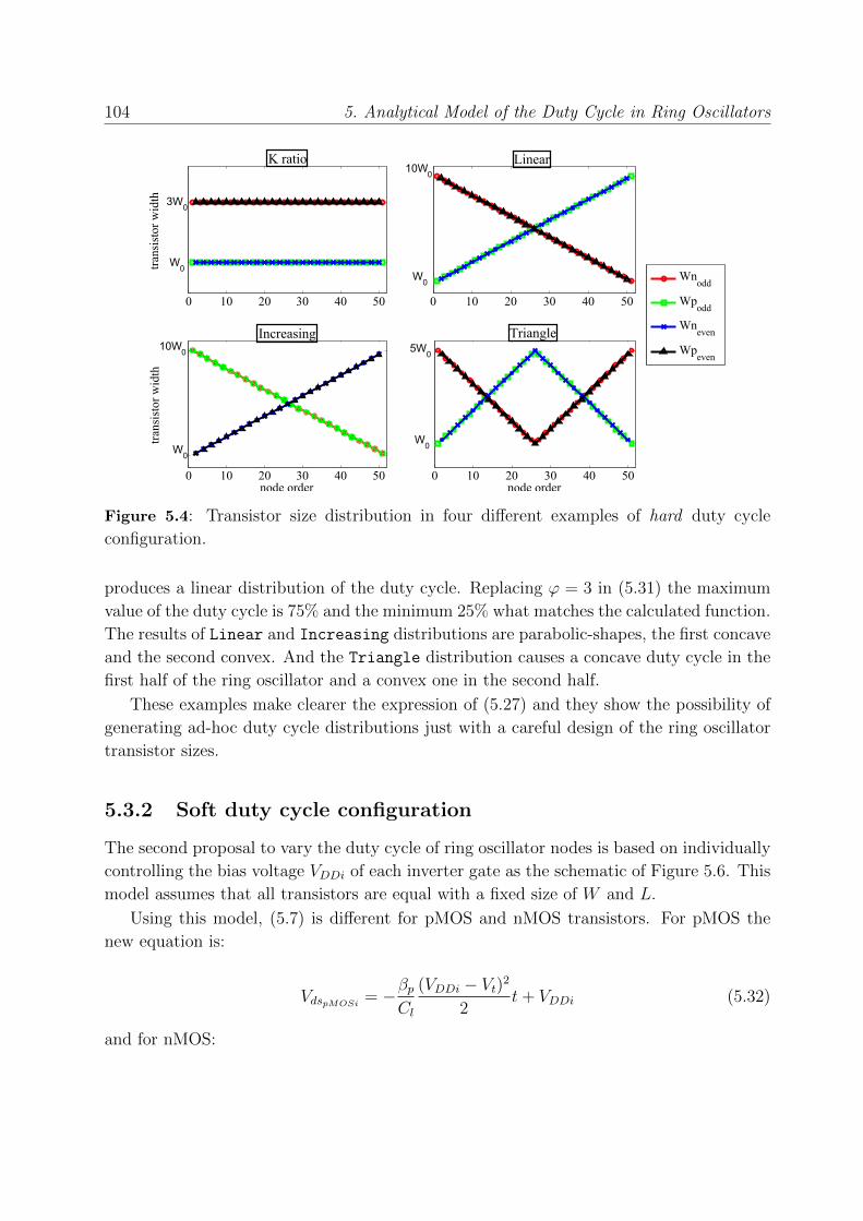
104 5. Analytical Model of the Duty Cycle in Ring Oscillators
0 10 20 30 40 50
K ratiotr
ansi
stor
wid
th
0 10 20 30 40 50
Linear
0 10 20 30 40 50
Increasing
node order
tran
sist
or w
idth
0 10 20 30 40 50
Triangle
node order
Wnodd
Wpodd
Wneven
Wpeven
W0
3W0
W0
10W0 5W
0
W0
10W0
W0
Figure 5.4: Transistor size distribution in four different examples of hard duty cycle
configuration.
produces a linear distribution of the duty cycle. Replacing ϕ = 3 in (5.31) the maximum
value of the duty cycle is 75% and the minimum 25% what matches the calculated function.
The results of Linear and Increasing distributions are parabolic-shapes, the first concave
and the second convex. And the Triangle distribution causes a concave duty cycle in the
first half of the ring oscillator and a convex one in the second half.
These examples make clearer the expression of (5.27) and they show the possibility of
generating ad-hoc duty cycle distributions just with a careful design of the ring oscillator
transistor sizes.
5.3.2 Soft duty cycle configuration
The second proposal to vary the duty cycle of ring oscillator nodes is based on individually
controlling the bias voltage VDDi of each inverter gate as the schematic of Figure 5.6. This
model assumes that all transistors are equal with a fixed size of W and L.
Using this model, (5.7) is different for pMOS and nMOS transistors. For pMOS the
new equation is:
VdspMOSi= −βp
Cl
(VDDi − Vt)2
2t+ VDDi (5.32)
and for nMOS:

5.3. Duty Cycle Configuration Models 105
0 5 10 15 20 25 30 35 40 45 5020
30
40
50
60
70
80
node order
duty
cyc
le (
%)
K ratioLinearIncreasingTriangle
Figure 5.5: Theoretical duty cycle distribution for the four different cases of study at every
internal node of a 51-stage ring oscillator.
Vdd1 Vddi VddN
node Nnode 1 node i
Figure 5.6: Schematic of a ring oscillator to independently control each inverter gate bias
voltage.
VdsnMOSi= −βn
Cl
(VDDi−1 − Vt)2
2t+ VDDi (5.33)
Thus the propagation delay is defined as the time lapsed to change Vds from VDDi to
VDDi+1/2. The solutions of (5.32) and (5.33) result in the rise and fall propagation times
which can be expressed by:
tpdri =(2VDDi − VDDi+1)Cl
βp(VDDi − Vt)2= ξp
(2VDDi − VDDi+1)
(VDDi − Vt)2(5.34)
tpdfi =(2VDDi − VDDi+1)Cl
βn(VDDi−1 − Vt)2= ξn
(2VDDi − VDDi+1)
(VDDi−1 − Vt)2(5.35)
with ξp and ξn:

106 5. Analytical Model of the Duty Cycle in Ring Oscillators
ξp =Clβp
and ξn =Clβn
(5.36)
We also define the same parameter λ = ξp/ξn = αp/αn = µn/µp for this model. Re-
placing (5.34) and (5.35) in (5.19) and (5.20), thigh and tlow at each node with individually
controlled bias voltages are:
thighi =αp(
i+N−12∑
j=i
(2VDDΓN (2j−1)− VDDΓN (2j)
)
(VDDΓN (2j−2)− Vt)2
+
+
i+N−32∑
j=i
(2VDDΓN (2j)− VDDΓN (2j+1)
)
λ(VDDΓN (2j)− Vt)2
)
(5.37)
tlowi =αp(
i+N−12∑
j=i
(2VDDΓN (2j−1)− VDDΓN (2j)
)
λ(VDDΓN (2j−1)− Vt)2
+
+
i+N−32∑
j=i
(2VDDΓN (2j)− VDDΓN (2j+1)
)
(VDDΓN (2j−1)− Vt)2
)
(5.38)
In this case the generalization of the duty cycle of (5.17) results in the expression:
di =
∑i+N−12
j=i
(2VDDΓN (2j−1)− VDDΓN (2j)
)
(VDDΓN (2j−2)− Vt)2∑N
j=1((2VDDj − VDDj+1)
(VDDj−1 − Vt)2+
(2VDDj − VDDj+1)
λ(VDDj − Vt)2)
+
+
∑i+N−32
j=i
(2VDDΓN (2j)− VDDΓN (2j+1)
)
λ(VDDΓN (2j)− Vt)2∑N
j=1((2VDDj − VDDj+1)
(VDDj−1 − Vt)2+
(2VDDj − VDDj+1)
λ(VDDj − Vt)2)
(5.39)
To validate this expression we evaluate the case of the same VDDi at each node, the
duty cycle is:
di =1
2+
(λ− 1)
2N(λ+ 1)(5.40)
what agrees with the previous proposal cases for γ = 1 or ϕ = 1. This case also tends to
a fixed duty cycle of 50% in every node of the ring oscillator.
The following examples of the soft duty cycle configuration are direct applications
of different bias voltage distributions to (5.39) for a 51-stage ring oscillator. Figure 5.7
represents the six different model cases theoretically calculated. For these applications,

5.3. Duty Cycle Configuration Models 107
10 20 30 40 50
V
10 20 30 40 50
10 20 30 40 50
V
10 20 30 40 50
10 20 30 40 50node order
V
10 20 30 40 50node order
VDDe
VDDo
P−Linear
K−ratio N−Linear
Cross−Linear
Double−TriangleTriangle
VDD
/2
VDD
VDD
/2
VDD
VDD
/η
VDD
VDD
VDD
/2
VDD
VDD
/2
VDD
VDD
/2
Figure 5.7: Examples of Vddi distributions of the soft duty cycle configuration.
bias voltages have been divided into odd —black lines— and even nodes —red lines—
(VDDo and VDDe). In the first example, K-ratio, the ratio between VDDo and VDDe is fixed
VDD = VDDe = ηVDDo. In the he N-Linear case VDD = VDDe and VDDe linearly decreases
from the first node to the last (VDDo(1) = VDD and VDDo(N) = VDD/2). The P-Linear
instance is the opposite of the last N-Linear example (VDD = VDDe, VDDo(1) = VDD/2 and
VDDo(N) = VDD). The Cross-Linear varies both voltages —VDDo and VDDe— linearly,
one decreases and the other increases. The Triangle example makes VDD = VDDe and VDDofirstly linearly increases up to the central node (VDDo(1) = VDD/2 and VDDo(
N−12
) = VDD)
and then it linearly decreases VDDo(N) = VDD/2. Finally, in the Double-Triangle one
voltage follows the distribution of the Triangle example and the other voltage follows just
the opposite.
The results of applying those voltage distributions in (5.39) are plotted in Figure 5.8.
Each different example produces different duty cycle distributions along the ring oscillator
nodes (linear, parabolic-shaped, sinusoidal-shaped). Therefore, it seems feasible to design
ad-hoc duty cycle distributions for the soft configuration model.

108 5. Analytical Model of the Duty Cycle in Ring Oscillators
5 10 15 20 25 30 35 40 45 500
20
40
60
80
100
nodegorder
duty
gcyc
leg(
%)
KgratioN−LinearP−LinearCross−LinearTriangleDouble−Triangle
Figure 5.8: Theoretical duty cycle distribution in the 6 different cases of soft configuration
study.
Vdd1 Vddi VddN
node Nnode 1 node ienable
Figure 5.9: Ring Oscillator with NAND gate to enable the oscillation.
5.4 Models Validation
The validation of the duty cycle configuration models introduced in Section 5.3 has been
carried out with Spectre simulation of a 40 nm commercial technology. Different schematics
have been tested in order to validate both approaches, hard and soft configurations. The
generic circuit whose parameters have been modified is depicted in Figure 5.9. The main
difference between this schematic and the one analyzed in Section 5.3 is the use of a NAND
gate that enables and disables the oscillation. The NAND transistors are implemented with
the minimum size fixed by the technology and they are not changed for all tests carried
out.

5.4. Models Validation 109
0
1
V0
1
V
0
1
V
0
1
V
0 1 2 3 4 5 60
1
time (ns)
V
node 1
node 10
node 25
node 40
node 51
Tthigh
Ttlow
Figure 5.10: Internal nodes of a 51-stage ring oscillator where different duty cycle are
observed.
5.4.1 Hard Configuration Validation
To validate the model based on the layout design the simulations are focused on three of
the four different examples presented in Section 5.3.1 —K-ratio, Linear and Triangle. In
Figure 5.10 some nodes are plotted to show the distribution of duty cycles in different nodes
within the chain of inverter gates. This specific case corresponds a K-ratio simulation of
a 51-stage ring oscillator with ϕ = 10. In the calculation of duty cycle the inverter and
non-inverter nodes are normalized according to the different definition of the duty cycle
for odd and even nodes made in Section 5.3. This means, for example in Figure 5.10, node
10 has a duty cycle close to 70% and for the node 51 the duty cycle is 85%, but for our
representations we consider node 10 as 70% and node 51 as 15%.
K-ratio simulations are divided into two different studies collected in Figures 5.11
and 5.12. In Figure 5.11 theoretical —dashed lines— and simulated —solid lines— results
of the K-ratio configuration model for different values of ϕ = 1, 2, ..., 10 are compared.
The simulations validate the linear duty cycle distribution previously predicted and they
show the variation of the slope distribution with respect to ϕ. Figure 5.12 plots the duty
cycle distributions for ring oscillators with different N and a fixed ϕ = 10. For small N
the impact of the NAND design is not negligible and a small alteration is observed. But
for N bigger than 20 stages the maximum and the minimum of the duty cycle distribution
changes less than 2% what concludes that the value of ϕ fixes the maximum and minimum
of duty cycle in the K-ratio model independently of the number of stages of the ring
oscillator, and the central node is always a clock signal with a 50% duty cycle.
The Linear configuration simulations correspond to the plot theoretically presented

110 5. Analytical Model of the Duty Cycle in Ring Oscillators
5 10 15 20 25 30 35 40 45 5010
20
30
40
50
60
70
80
90
node order
duty
cyc
le (
%)
=1
=2
=3
=4
=5
=6
=7
=8
=9
=10
Figure 5.11: 51-stage ring oscillator duty cycle distribution for different ϕ values. Solid
lines are simulation results and dashed lines are theoretical values.
0 10 20 30 40 50 60 70 80 90 10010
20
30
40
50
60
70
80
90
node order
duty
cyc
le (
%)
Nº
of s
tage
s
10
20
30
40
50
60
70
80
90
Figure 5.12: Duty cycle of a K-ratio distribution for ring oscillators with different number
of stages.
in Section 5.3.1 with ϕ(1) = ϕ0 = 10, ϕ(N) = 1/ϕ0 = 1/10, Wpo(1) = W0 = 120 nm
and Wpo(N) = ϕ0W0 = 1200 nm for different odd N stages from 3 to 99. The results
of these simulations are represented in Figure 5.13 compared to the calculated solutions
from (5.27). In this figure the x-axis represents the nodes normalized to easily compare
the distributions with different number of nodes. The normalization is defined by i/N in
percentage. As the previous figure, the impact of the minimum size NAND gate used for
the simulation has a visible impact for the accuracy of the model in small ring oscillator,

5.4. Models Validation 111
0 10 20 30 40 50 60 70 80 90 10020
25
30
35
40
45
50
55
duty
scyc
les(
%)
nodesordersnormalizeds(%)
Nºs
ofss
tage
s
10
20
30
40
50
60
70
80
90
Figure 5.13: Duty cycle for the linear distribution example. Solid lines are simulation
results and dashed lines are theoretical values.
0 10 20 30 40 50 60 70 80 90 10035
40
45
50
55
60
nodesordersnormalizeds(%)
duty
scyc
les(
%)
Nºs
ofss
tage
s
10
20
30
40
50
60
70
80
90
Figure 5.14: Duty cycle for the triangular distribution case. Solid lines are simulation
results and dashed lines are theoretical values.
but for a big enough number of stages, N , the model and the simulations tend to the same
distribution with absolute error less than 2%.
The last simulations that validate our hard duty cycle configuration test the Triangle
design case. Figure 5.14 plots the result of this example validation. In this case the absolute
error of (5.27) is also less than 2% at every node of the ring oscillator for increasing N
stages.

112 5. Analytical Model of the Duty Cycle in Ring Oscillators
5 10 15 20 25 30 35 40 45 5010
20
30
40
50
60
70
80
90
node order
duty
cyc
le (
%)
VDDo
=1.1 V
VDDo
=1.05 V
VDDo
=1 V
VDDo
=0.95 V
VDDo
=0.90 V
VDDo
=0.85 V
VDDo
=0.8 V
VDDo
=0.75 V
VDDo
=0.7 V
Figure 5.15: 51-stage ring oscillator duty cycle distribution for different η values. Solid
lines are simulation results and dashed lines are theoretical values.
5.4.2 Soft Configuration Validation
The validation of the soft configuration follows the same steps that the hard one. In this
case, the simulations carried out concerned the examples of K-ratio and Double-Triangle.
K-ratio simulations are plotted in Figure 5.15. As was expected from Figure 5.8,
the duty cycle distribution along the ring oscillator is linear. The value of VDDo behaves
likewise the value of ϕ in the hard configuration fixing the maximum and the minimum of
the duty cycle distribution or changing its slope.
Finally, in Figure 5.16 the Double-Triangle simulated results are depicted. The
sinusoidal-shaped distribution previously anticipated is confirmed by the simulations. As
in previous examples, the model improves its accuracy with increasing number of stages,
N , and from 30 stages, the error of the model is close to 3%.
Both models have been simulated and validated and the hypothesis of designing a ring
oscillator with internal duty cycles signals different from 50% have been confirmed. The
simulations and equations prove also that fully-configurable duty cycle distributions can
be implemented with our proposed models.
5.4.3 Transistor Mismatch
Since our proposal relies on varying the duty cycle of ring oscillator nodes, the validation
of the models must include a study of fabrication mismatch impact. The fabrication of
integrated circuits is not a perfect process and the stochastic nature of the physical pro-
cesses implies that identical designs have random differences in their performance. Device
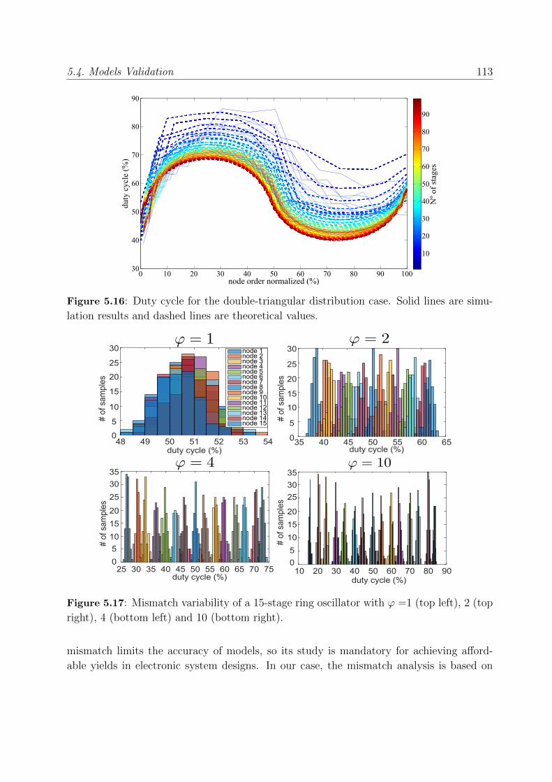
5.4. Models Validation 113
0 10 20 30 40 50 60 70 80 90 10030
40
50
60
70
80
90
duty
scyc
les(
%)
nodesordersnormalizeds(%)
Nºs
ofss
tage
s
10
20
30
40
50
60
70
80
90
Figure 5.16: Duty cycle for the double-triangular distribution case. Solid lines are simu-
lation results and dashed lines are theoretical values.
duty cycle (%)48 49 50 51 52 53 54
# of
sam
ples
0
5
10
15
20
25
30 node 1node 2node 3node 4node 5node 6node 7node 8node 9node 10node 11node 12node 13node 14node 15
duty cycle (%)35 40 45 50 55 60 65
# of
sam
ples
0
5
10
15
20
25
30
duty cycle (%)25 30 35 40 45 50 55 60 65 70 75
# of
sam
ples
0
5
10
15
20
25
30
35
duty cycle (%)10 20 30 40 50 60 70 80 90
# of
sam
ples
0
5
10
15
20
25
30
35
Figure 5.17: Mismatch variability of a 15-stage ring oscillator with ϕ =1 (top left), 2 (top
right), 4 (bottom left) and 10 (bottom right).
mismatch limits the accuracy of models, so its study is mandatory for achieving afford-
able yields in electronic system designs. In our case, the mismatch analysis is based on

114 5. Analytical Model of the Duty Cycle in Ring Oscillators
duty cycle (%)25 30 35 40 45 50 55 60 65
# of
sam
ples
0
5
10
15
20
25
30
35node 1node 2node 3
duty cycle (%)25 30 35 40 45 50 55 60 65 70
# of
sam
ples
0510
152025
3035
4045
node 1node 2node 3node 4node 5
duty cycle (%)25 30 35 40 45 50 55 60 65 70 75
# of
sam
ples
0
5
10
15
20
25
30
35
duty cycle (%)20 30 40 50 60 70 80
# of
sam
ples
051015202530354045
N=15 N=45
N=5N=3
node 15node 3 node 45node 1 node2
Figure 5.18: Mismatch variability of an N-stage ring oscillator with ϕ =4 and N=3(top
left), 5 (top right), 15 (bottom left) and 45 (bottom right).
MonteCarlo simulations of 100 different samples according to the manufacturer variability
models.
The presented analysis of mismatch is carried out for the hard configuration model and
the K-ratio structure. The results are extrapolated to the rest of potential configurations.
On the one hand, we explore the impact of ϕ (Wpo = Wne = ϕWpe = ϕWno) on the
duty cycles at each node. Hence, we fixed the value of N to 15 stages and we changed
ϕ. The results of these simulations are depicted in Figure 5.17. For this specific design,
mismatch can alter the mean value of the duty cycle by ±1% using the minimum transistor
and it negligibly decreases for bigger gate widths. With the correct configuration values
the design works properly for node identification reading its duty cycle.
On the other hand, we analyze the duty cycle variability caused by mismatch in in-
creasing ring oscillators. Figure 5.18 is the result of fixing ϕ = 4 and changing N . In
this case, the variability of the duty cycle is inversely proportional to the number of ring
oscillator stages. With a minimum 3-stage ring oscillator, the transistor mismatch implies
a variability of ±2.5% from its nominal value, and with a bigger ring oscillator, 45-stages,
it is reduced to ±0.5%.
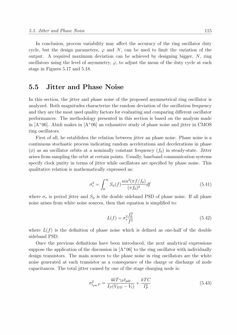
5.5. Jitter and Phase Noise 115
In conclusion, process variability may affect the accuracy of the ring oscillator duty
cycle, but the design parameters, ϕ and N , can be used to limit the variation of the
output. A required maximum deviation can be achieved by designing bigger, N , ring
oscillators using the level of asymmetry, ϕ, to adjust the mean of the duty cycle at each
stage in Figures 5.17 and 5.18.
5.5 Jitter and Phase Noise
In this section, the jitter and phase noise of the proposed asymmetrical ring oscillator is
analyzed. Both magnitudes characterize the random deviation of the oscillation frequency
and they are the most used quality factors for evaluating and comparing different oscillator
performances. The methodology presented in this section is based on the analysis made
in [A+06]. Abidi makes in [A+06] an exhaustive study of phase noise and jitter in CMOS
ring oscillators.
First of all, he establishes the relation between jitter an phase noise. Phase noise is a
continuous stochastic process indicating random accelerations and decelerations in phase
(φ) as an oscillator orbits at a nominally constant frequency (f0) in steady-state. Jitter
arises from sampling the orbit at certain points. Usually, baseband communication systems
specify clock purity in terms of jitter while oscillators are specified by phase noise. This
qualitative relation is mathematically expressed as:
σ2τ =
∫ ∞0
Sφ(f)sin2(πf/f0)
(πf0)2df (5.41)
where στ is period jitter and Sφ is the double sideband PSD of phase noise. If all phase
noise arises from white noise sources, then that equation is simplified to:
L(f) = σ2τ
f 30
f 2(5.42)
where L(f) is the definition of phase noise which is defined as one-half of the double
sideband PSD.
Once the previous definitions have been introduced, the next analytical expressions
suppose the application of the discussion in [A+06] to the ring oscillator with individually
design transistors. The main sources to the phase noise in ring oscillators are the white
noise generated at each transistor as a consequence of the charge or discharge of node
capacitances. The total jitter caused by one of the stage charging node is:
σ2tpdrP
=4kTγP tpdr
IP (VDD − Vt)+kTC
I2P
(5.43)

116 5. Analytical Model of the Duty Cycle in Ring Oscillators
where k is the Boltzmann’s constant, T is the temperature, γ is a technology factor with
a value between 0.6 and 0.9 and IP is the pMOS source-drain current. (5.43) has two
different terms, the first one is the noise generated by the integration of the noise arises
from the pMOS transistor in the charging capacitance. And the second term comes from
the initial noise deposited by the pull-down nMOS transistor. Respectively, the jitter of
the discharge of a node capacitance is:
σ2tpdfN
=4kTγN tpdf
IN(VDD − Vt)+kTC
I2N
(5.44)
All of these sources are independent and uncorrelated, therefore the total variance of
the period jitter is:
σ2τ =
N∑i=1
(σ2tdiN
+ σ2tdiP
) (5.45)
From (5.43) and (5.44):
σ2τ =
N∑i=1
(4kTγN tpdfi
INi(VDD − Vt)+kTC
I2Ni
+4kTγP tpdri
IPi(VDD − Vt)+kTC
I2Pi
) (5.46)
Using (5.9):
σ2τ =
N∑i=1
(4kTγN tpdfi
INi(VDD − Vt)+
2kT tpdfiINiVDD
+4kTγP tpdri
IPi(VDD − Vt)+
2kT tpdriIPiVDD
) (5.47)
and making γN = γP to simplify:
σ2τ = κ
N∑i=1
(tpdfiINi
+tpdriIPi
) (5.48)
where κ is only dependent on the technology and defined as:
κ = 2kT ((2γ + 1)VDD − VtVDD(VDD − Vt)
) (5.49)
Thus, the phase noise according to (5.42):
L(f) = κ(f 3
0
f 2)
N∑i=1
(tpdfiINi
+tpdriIPi
) (5.50)
In [A+06] the phase of a CMOS ring oscillator with equal delay stages is defined as:
L(f) =2kT
IDSAT(
1
VDD − Vt(γN + γP ) +
1
VDD)(fof
)2 (5.51)
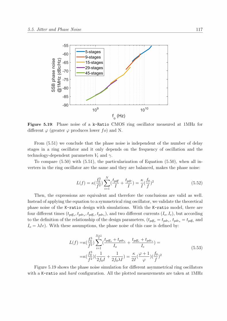
5.5. Jitter and Phase Noise 117
fo
(Hz)109 1010
SS
B2p
hase
2noi
se@
1MH
z2(d
Bc/
Hz)
-90
-85
-80
-75
-70
-65
-60
-55
5-stages9-stages15-stages29-stages45-stages
Figure 5.19: Phase noise of a k-Ratio CMOS ring oscillator measured at 1MHz for
different ϕ (greater ϕ produces lower fo) and N.
From (5.51) we conclude that the phase noise is independent of the number of delay
stages in a ring oscillator and it only depends on the frequency of oscillation and the
technology-dependent parameters Vt and γ.
To compare (5.50) with (5.51), the particularization of Equation (5.50), when all in-
verters in the ring oscillator are the same and they are balanced, makes the phase noise:
L(f) = κ(f 3
0
f 2)
N∑i=1
(tpdfI
+tpdrI
) =κ
I(f0
f)2 (5.52)
Then, the expressions are equivalent and therefore the conclusions are valid as well.
Instead of applying the equation to a symmetrical ring oscillator, we validate the theoretical
phase noise of the K-ratio design with simulations. With the K-ratio model, there are
four different times (tpdfo , tpdro , tpdfe , tpdre), and two different currents (Io, Ie), but according
to the definition of the relationship of the design parameters, (tpdfo = tpdre , tpdro = tpdfe and
Io = λIe). With these assumptions, the phase noise of this case is defined by:
L(f) =κ(f 3
0
f 2)
N+12∑i=1
(tpdfo + tpdre
Io+tpdfe + tpdro
Ie) =
=κ(f 3
0
f 2)(
1
2f0I+
1
2f0λI) =
κ
2I(ϕ+ 1
ϕ)(f0
f)2
(5.53)
Figure 5.19 shows the phase noise simulation for different asymmetrical ring oscillators
with a K-ratio and hard configuration. All the plotted measurements are taken at 1MHz
118 5. Analytical Model of the Duty Cycle in Ring Oscillators
from the oscillator frequency. In the figure, five different frequency overlapped ring oscil-
lators are presented, with 5, 9, 15, 29 and 45 stages. With a fixed number of stages, the
frequency is controlled by ϕ. Each colored line represents the frequency for ϕ from 1 to
10. Lower values of ϕ produce higher oscillation frequencies. The aggregated phase noise
function forms a continuous line that validates (5.51). The phase noise of the ring oscil-
lator is independent of the number of stages but it depends on the oscillation frequency.
The tradeoff between a faster oscillator and a good performance in terms of phase noise is
maintained in the proposed ring oscillator.
5.6 Discussion
The model of the duty cycle of ring oscillators presented in this chapter has followed a
simple approach to ease the understanding of the foundations of the configurable duty
cycle feature. Despite the explained simplifications, the validation of the model, with a
40 nm commercial technology, has evidenced that the accuracy of the model is very good
with an absolute error of 3% in a medium size ring oscillators.
However, the accuracy can be improved avoiding some of the assumed limitations. In
the development of our model we have made three main simplifications. First, we have
used the long-channel model of MOS transistors. Second, we have only used the saturation
region of that model to define the propagation time delay. And third, we have modeled
the capacitance at each node of a ring oscillator only as the gate capacitance of the next
stage.
To overcome these three simplifications and to improve the accuracy of the model, the
next steps would be:
• Taking into account the non-ideal effects of MOS transistors current model: mobility
degradation, velocity saturation or channel length modulation.
• Modeling the node capacitance by a more complex model which includes the input-
output coupling capacitance, the capacitance dependence on the layout or a more
complex model of gate capacitance [XDH+03].
• Including a more accurate definition of the charging and discharging of nodes accord-
ing to each region of the current model.
The evolution of our model would be parallel to the improvement process followed by
the studies that have defined the propagation delay of CMOS inverters which are sum-
marized in the work of Rosello and Segura [RS04]. In that work, the authors reviewed
the different techniques proposed to accurately define the propagation delay of a CMOS
inverter [HOT98,BNK98,KAKAK03], and they proposed a new model to go a step further.

5.7. Conclusions 119
5.7 Conclusions
This chapter is an in-depth study of the well-known electronic system ring oscillator. To
the best of our knowledge, so far ring oscillators have been used for several applications
but for all of them the system output is a clock signal with 50% duty cycle. Our work sets
the analytical basis for understanding and designing a ring oscillator whose outputs are
clock signals with a duty cycle different from 50% and fully-configurable.
To vary the output duty cycle, we have begun analyzing the possible design parameter
that affect the duty cycle. This analysis have revealed two different values, the size of
transistors and the bias voltage. According to those two possibilities, we have presented
two models in order to vary the output duty cycle, a first model, hard, is based on layout
design, focusing on transistor sizing along the chain of inverter gates, and the second model,
soft establishes a relation between duty cycle and different bias voltage schemes with no
area overhead.
Additionally, these models are validated by simulation analysis using a commercial
40 nm technology and they are also characterized in terms of mismatch variability and
phase noise performance. The variability has shown a dependency with the number of
stages of the ring oscillator which can reduce it from 2.5% with minimum size to less than
0.5% in a 45-stage ring oscillator. Regarding the phase noise, our model fits with previous
ring oscillator works which concluded that the phase noise is independent on the stages of
a ring oscillator but dependent on its frequency.
5.8 Related Publications
• J. Agustin and M. Lopez-Vallejo, ”An In-Depth Analysis of Ring Oscillators: Ex-
ploiting Their Configurable Duty-Cycle,” in IEEE Transactions on Circuits and Sys-
tems I: Regular Papers, vol. 62, no. 10, pp. 2485-2494, Oct. 2015.
doi: 10.1109/TCSI.2015.2476300


Chapter 6
Application of the Duty Cy-cle Ring Oscillator Model toImprove PUF Reliability

Chapter 6
Application of the Duty Cycle RingOscillator Model to Improve PUF Reliability
6.1 Introduction
The advance of electronic industry has enhanced the ubiquity of electronic systems. Fur-
thermore, the IoT era tends to connect as many electronic systems as possible. Following
this trend, as the number of networked smart objects, programs, and data is constantly in-
creasing, there is an equally growing demand to ensure the security and reliability of these
units [RDK12]. Therefore, the security hardware has become a hot topic for researchers
during the last decade. Three main applications are referred when this term is applied to
electronic systems: identification, authentication and key generation. In identification a
known ID is uniquely assigned to an unknown entity. Authentication is the procedure to
verify a claimed ID of an entity. And key generation is a fundamental block of modern
cryptographic systems to secure communication protocols.
For many years, security hardware applications trusted on Non-Volatile Memories
(NVMs) [STP08] to store the secure keys without requiring constant power. However,
several works have proved the vulnerability of digital keys in NVMs to invasive physical
attacks [BS97, Sko05]. Dealing with this vulnerability entails the implementation of com-
plex additional circuits that result in area and power overhead. In this context, Physically
Unclonable Functions (PUFs) were postulated 15 years ago and they have emerged as very
promising primitives for security hardware since then.
To solve the drawbacks of NVM based security applications, PUFs exploit the ability
of hardware devices to store or generate a unique, secure and unpredictable key in order
to avoid hacker attacks or unlicensed use of hardware designs. Even though all chips are
manufactured in huge quantities, every chip is unique because of the intrinsic variability
of fabrication processes. Indeed, as the technology keeps scaling down, such differences
become more and more significant, affecting not only the chip performance, but circuit
functionality too. Therefore, in the past couple of decades, there have been many efforts
to reduce or control manufacturing variability. Simultaneously, researchers have discovered

6.1. Introduction 123
methods to put such variation for good uses in security applications [ZQLZ14]. Compared
to the NVM approach [HYKD14] PUF hardware is simpler and requires less power con-
sumption; since the chip must be powered on to operate and PUFs usually work for a
short period of time, any physical attack is harder; invasive attacks modify the physical
characteristics, so their use would modify the PUF outputs; and memory based systems
are more expensive to fabricate.
Different definitions have been proposed for PUFs, and recently, in [PM15], Plaga and
Merli have unified previous works to define a PUF as a physical information-storage system
that is protected by a security mechanism which: 1) has the security objective to render
it more difficult to duplicate a precisely described storage functionality of the system
in another, separate system. 2) is meant to remain effective against an active attacker
with temporary physical access to the whole system in its original form. Many hardware
systems have been presented that fit into this definition. Among all of them, one of the
most common and mature designs uses ring oscillators as the basic structure. Hence, ring
oscillators are playing a fundamental role in the development of PUFs.
Unfortunately, as in any other design, the performance of the electronic circuits used
in PUFs are intrinsically dependent on external variables. Among all of them, the most
relevant ones are temperature, bias voltage and aging. The effects of all of these variables
in the performance of ring oscillators have been extensively studied, specially how they
affect their output frequencies. In the particular application of PUFs, the reliability of the
system is highly compromised by the variation of circuit outputs.
As has been shown in this Thesis, the radiation is also an important source of unreliabil-
ity. It has also been mentioned how the shrinking technology is enhancing the occurrence
of radiation effects in environments where they were negligible. Since PUFs are very crit-
ical blocks whose failure would affect the integrity of the whole system, we introduce the
study of radiation impact in the study of PUF reliability.
In this chapter we propose an improvement on ring oscillator based PUFs. Conven-
tional RO PUFs measure the output frequency of several identical ring oscillators and they
generate an output depending on their relationships. Instead of using this approach, we
design a PUF based on measuring differences in the duty cycle of different signals. Chap-
ter 5 has already introduced the methodologies to fully configure the duty cycle of ring
oscillators. Our PUF topology allows to increase the potential relationships between dif-
ferent ring oscillator outputs and it also improves their robustness by using the duty cycle
instead of the frequency magnitude. Furthermore, we have proven that the implementation
of a configurable duty cycle ring oscillator makes them fully tolerant to SETs in Chapter 4.
The rest of the chapter is organized as follows. First, in Section 6.2 the foundations
of PUF and related work is presented. The RO PUF and its variants and advances are
summarized in Section 6.3. Sections 6.4 and 6.5 describe our PUF proposal by exploring
the potential of the duty cycle as output parameter for PUFs, explaining the proposed ar-

124 6. Application of the Duty Cycle Ring Oscillator Model to Improve PUF Reliability
PUFChallenge(C)
Response(R)
Same Challenge
Different PUF
DifferentResponse
C PUF1 R1
C PUF2 R2
C PUF3 R3
=
=
=
Different Challenge
Same PUF
Different Response
C1 PUFx R1
C2 PUFx R2
C3 PUFx R3
=
=
=
=
Same Challenge
SamePUF
SameResponse
C PUFx R
C PUFx R
C PUFx R
=
=
=
=
=
=
=
Figure 6.1: PUF basic operation as a CRP pair system and its ideal operation.
chitecture and presenting the simulation results for nominal conditions and environmental
variations. In Section 6.6 we explain the fabricated circuit to validate the PUF proposal
and the test plan for the future test campaign. Finally, in Section 6.7 the main conclusions
of this chapter are drawn.
6.2 Related Work
6.2.1 PUF Foundations
PUFs are Challenge Response Pair (CRP) architectures [TS07]. These systems are char-
acterized for generating a response when a specific challenge drives their input. PUF
responses are completely unique for every chip thanks to the uncontrollable manufacturing
process variations. Figure 6.1 explains the fundamental operation of a CRP architecture.
The first condition of these systems is that for the same challenge and the same PUF,
the response must be consistently the same. Any other result would be an error. Other
characteristic is that given a challenge, the response for the application of that challenge
to different PUFs must be different. And finally, the use of the same challenge to excite
different PUFs will also generate different responses. Moreover, all the CRPs have to be
completely unforeseeable.
To compare different types and designs of PUFs, it is necessary to define a set of
parameters that quantify their features. To this purpose, in [MGS13], Maiti presents the
most important quality factors of PUFs that we summarize in this section: randomness,
reliability and robustness.
6.2. Related Work 125
Randomness
The randomness of a PUF is measured by statistically analyzing the CRPs for a set of
challenges in different instances of the same PUF implementation. The randomness is
analyzed by calculating three parameters:
• Uniqueness. The uniqueness is a measurement of how unique are the responses
generated from different chips. It is estimated by the average value of the inter-die
Hamming Distance (HD) of responses. Where the HD is a parameter of information
theory defined as the number of different bits of two words of the same bitwidth.
For k different PUF chips with responses R of n bits, the expression that defines the
uniqueness is:
Uniqueness =2
k(k − 1)
k−1∑i=1
k∑j=i+1
HD(Ri, Rj)
n(6.1)
• Uniformity. It is a random variable that measures the distribution of ’0’s and ’1’s
in the response of a particular PUF. As the response of PUF must be completely
random, the number of ’0’s and ’1’ should be ideally the same. It can be calculated
by the mean of the Hamming Weights of a set of responses:
Uniformity =1
n
n∑l=1
rl (6.2)
where rl is the l-th bit of the response.
• Bit aliasing. The aliasing refers to the generation of similar responses for different
PUFs that can derive in authentication errors. It is estimated by the average number
of ’0’s and ’1’s of the l-th bit of the n bit responses among k different chips.
(BitAliasing)l =1
k
k∑i=1
ri,l (6.3)
where ri,l is the l-th bit of a response of PUFi.
Attending to the three definitions, the ideal value for all of the parameters is 50 %. It
means that the probability of every response bit to be ’0’ or ’1’ is the same and independent
on the PUF device, bit position or the rest of bits within the same response.

126 6. Application of the Duty Cycle Ring Oscillator Model to Improve PUF Reliability
Reliability
The randomness is able to measure the characteristics of PUF responses. These charac-
teristics are expected to be static, but they can actually vary as a consequence of external
factors. So far, the factors that have been taken into account by most of the studies are
temperature variation [MRV+12a,Che15] and stability of bias voltage [MRV+12b,ZFC+14].
Moreover, aging has also been included in some recent analysis [MS14,GN14]. Aging effects
produce temporal degradation of chips that can provoke irreversible changes destroying the
device functionality.
The reliability of PUFs measures their dependency with respect to those factors. It can
be measured by the intra-chip Hamming Distance. If a PUF i generates a n-bit response,
Ri, at nominal conditions, it should generate the same response R′i at different conditions
and time t. With this notation, given m measurements of the response of a specific PUF
for the same challenge, the reliability of that PUF can be calculated as:
Realiability = 1− 1
m
m∑t=1
HD(Ri, R′i,t))
n(6.4)
As mentioned in the introduction of this chapter, radiation has become an important
source of unreliability. While it has remained out of the scope of previous PUF works, its
increasing relevancy, even at ground level, makes it an important factor to consider. In this
thesis, both of the categories of radiation effects, cumulative and SEE have been analyzed.
Their interaction with electronic circuits has revealed some of the possible effects, such
as the variation of oscillation frequency by TID, that clearly affect the PUF performance.
To the best of our knowledge, it is the first time that a PUF is characterized in terms of
radiation effects.
Robustness
The robustness refers to the characteristic of PUFs to keep their secret from malicious
attacks. There is no qualitative variable to measure the robustness because there are
only two possibilities, it can be “hacked” or it cannot. Instead of a parameter, PUFs
can be robust against certain types of attacks. At the same time, the attack suitable to
force a PUF is highly dependent on its implementation. Many different attacks have been
developed to show the weakness of almost every proposal. Although they are specific for
each particular PUF, the types of attacks are usually divided into four different categories:
• Active attack. Active attacks are based on altering the normal operation of the
system in order to deduce the CRPs [BM09]. By manipulating the system or its en-
vironment, the response is modified and monitored. A relationship can be established
between the variation of responses and the inner mechanism of the PUF. This type

6.2. Related Work 127
of attacks can be invasive or non-invasive depending on the possibility of destruction
of the device during the attack [NSHB13].
• Passive attack. Passive attacks observe and collect information of the working PUF
instead of trying to change it [BK+14]. A PUF may be attacked by using side-channel
attack information such as power consumption or electromagnetic radiation while it
is in operation.
• Replay attack. This attack replaces a CRP, copied during the phase of authentica-
tion, to use it instead of the original PUF [ZLQ15]. If the security system only uses
each CRP once, this attack is useless. However, this condition makes challenging the
construction of a PUF with a great number of CRPs.
• Modeling attack. The physical behavior of a PUF can be modeled mathemati-
cally [RvD13, MRMK13]. This way, an equivalent circuit to a specific PUF can
be designed to replace the genuine device. PUF randomness is highly linked with the
difficulty of modeling it as the variations come from physical phenomena.
6.2.2 Types of PUF
Once the concept of PUFs and the quality factors that allow to characterize them have
been introduced, this section summarizes the types of PUFs that have been proposed in
previous works. The amazing popularity of PUFs during the last decade has contributed
to the generation of a huge and heterogeneous number of proposals. Together with these
proposals, some works have tried to create a taxonomy of the devices resulting in different
types of classification:
• Based on the implementation technology: non-silicon versus silicon.
• Based on a more general set of physical properties: nonintrinsic versus intrinsic.
• Based on the properties of their CRP behavior: weak versus strong.
Silicon/Non-Silicon
Non silicon PUF refers to the proposals that are implemented with non-electronic tech-
nology such as optical [PRTG02] or magnetic [DSR+15] PUFs. On the other hand, silicon
PUFs use the uncontrollable variations of semiconductor electronic manufacturing pro-
cesses to generate the unique signature for each IC. According to the different sources of
variation, silicon PUFs are also divided into three different categories: analog electronic
PUFs, memory-based PUFs [GK14], and delay-based PUFs [MS09]. Since silicon PUFs

128 6. Application of the Duty Cycle Ring Oscillator Model to Improve PUF Reliability
Table 6.1: Classification of previous works according to different features.
PUF ProposalSilicon/
Non-Silicon
Intrinsic/
Nonintrinsic
Weak/
Strong
Optical PUF [PRTG02] Non-Silicon Nonintrinsic Strong
Coating PUF [STO05] Silicon Nonintrinsic Strong
SRAM PUF [MTV09] Silicon Intrinsic Weak
Butterfly PUF [KGM+08] Silicon Intrinsic Strong
Ring Oscillator PUF [SD07] Silicon Intrinsic Weak
Arbiter PUF [FSF+11] Silicon Intrinsic Strong
RRAM PUF [MRFA15] Non-Silicon Intrinsic Weak
Nanotube PUF [LLZH16] Non-Silicon Nonintrinsic Strong
Magnetic PUF [DSR+15] Non-Silicon Nonintrinsic Strong
are fully integrable with all electronic circuits, they have been raised as the main type of
PUF architectures in research works.
Intrinsic/Nonintrinsic
A PUF is considered intrinsic if it fulfills both of these conditions: 1) Its evaluations are
performed internally by embedded measurement equipment. It means that the response is
generated inside the chip and there is no need to make any additional processing outside the
chip. 2) Its random device specific features are implicitly introduced during its production
process. This condition separates the PUFs that require additional processes to enhance
the variability of the conventional fabrication process.
Weak/Strong
Depending on the number of CRPs that a PUF produces, it can be classified into two
general categories: weak and strong. Weak PUFs generate a limited number of CRPs, so
they can be fully read out within a very short time. In this type of PUFs, the number of
CRPs is linearly or polynomially dependent on the number of challenge bits. Opposite,
strong PUFs can be driven by almost an unlimited amount of challenges. A strong PUF
needs to prove its security under a strong attack model. Their very large number of CRPs
avoid using malicious attacks based on brute force within a realistic time. They are also
resilient to modeling attacks making really hard to predict the response of a PUF to a
randomly selected challenge.
Table 6.1 outlines and classifies some of the proposals of the literature for PUF imple-
mentations according to these three different classifications.

6.3. Ring Oscillator PUF 129
Challenge
Response>
Counter 1
Counter 2
RO 1
RO n
Enable i
Enable
Figure 6.2: Conventional RO PUF architecture based on frequency variability [MS09].
6.3 Ring Oscillator PUF
A Ring Oscillator PUF (RO-PUF) is a silicon, intrinsic and weak PUF that generates
the response using the output frequencies of ring oscillators. It is silicon because it is
implemented using on-chip oscillators. It is intrinsic as it is based on measuring process
variations on the frequencies and the responses are evaluated within the PUF. And it is
weak since it can generate log2(n!) independent responses from a PUF with n identical
ring oscillators.
The first proposal of using a ring oscillator to build a PUF was made by Gassend et
al. [GCvDD02]. They proposed to use a single ring oscillator whose output drives a counter
that monitors the number of cycles in a fixed time interval. This value is quantized and
converted into the response of the PUF. That implementation proved to be valid as the
frequency of equal implementations on different chips suffered enough variation to generate
unique responses. However, the influence of environmental conditions on the frequency of
ring oscillators is well-known and the unreliability of this proposal was immediately pointed
out.
Suh and Devadas [SD07] proposed an alternative architecture to the Gassend et al.
[GCvDD02] approach. Their proposal uses more than only one ring oscillator and considers
the relative frequencies of pairs of oscillators instead of using the absolute value of a single
oscillator. It follows the architecture depicted in Fig. 6.2. It is made of n identical N -stage
ring oscillators. The challenges of this PUF consist in selecting a pair of ring oscillators (a,b)
and comparing their output frequencies expecting a deviation due to process variations.
Then, if fa is greater than fb the response is ‘1’, otherwise the output is ‘0’.
The implementation of Suh and Devadas has become one of the most studied architec-
130 6. Application of the Duty Cycle Ring Oscillator Model to Improve PUF Reliability
tures of silicon PUFs and it appears in all comparisons for new PUF approaches. Moreover,
it is the base for many proposals that try to solve the problems that this RO-PUF presents.
The first problem is the small number of independent CRPs. If a RO-PUF is made of
n ring oscillators, a total of(n2
)= n(n−1)
2are the potential bit responses. However, those
evaluations are not completely independent, for instance, if fa is greater than fb and fb is
greater than fc then fa is directly greater than fc and the response is not unforeseeable as it
is required in PUFs. Therefore, the real number of independent comparison of n frequencies
decreases to log2(n!). At the same time, this number fixes a maximum theoretical limit
which is achieved depending on the specific implementation. Finally, just n/2 response
bits are guaranteed to be fully independent. In [SD07] the authors even reduce the number
of responses in order to improve the reliability by a technique called 1-out-of-k-masking
where only bnkc ring oscillators are used.
To solve this problem, but keeping the upper limit, different modifications have been
proposed, such as the PUF designed by Maiti et al. [MS09], where the inverters of ring
oscillator stages are configurable to increase the intrinsic process variations. Another ap-
proach is presented by Maiti et al. [MKS12] where the number of CRPs is increased by
using an identity-mapping function that post-processes the output frequencies to increase
the entropy.
Another important problem is the reliability of the RO-PUF. Many works have shown
very good quality factors of RO-PUF implementations at nominal conditions. However,
environmental and aging variations lead the PUF to generate unreliable bits. In [GN14],
the effects of aging in RO-PUFs are studied and in [RFFT14] a possible solution to improve
its resilience is shown. The solution in [RFFT14] tries to reduce the degradation of ring
oscillators by controlling the Negative-Bias Temperature Instability (NBTI) and the Hot
Carrier Injection (HCI) phenomena in pMOS and nMOS. Those phenomena are the most
relevant agents in the degradation of transistors as a consequence of aging. Vivekraja and
Nazhandali [VN09] showed how the bias voltage variation is able to decrease the uniqueness
of RO-PUFs from the ideal 50% to almost 25%. The temperature is also a problem to keep
the reliability of the RO-PUF close to 100% as it is studied in [YQ09] where a solution is
proposed. This solution is based on defining zones of secure operation for each pair of ring
oscillators.
Many works are focused on compromising the robustness of new PUF proposals as they
are intended to be placed in security systems. The maturity of the RO-PUF has led to
the development of several attempts to break its “secret” using the different approaches
introduced in the previous section. For example, Ruhrmair et al. [RSS+13] showed that
modeling attacks using machine learning techniques can foresee RO-PUF responses to a
given challenge with prediction rates up to 99%. Merli et al. [MSSS11] pointed out that
a side channel attack is possible to RO-PUFs. They analyzed the frequencies of ring
oscillators by measuring the electromagnetic radiation together with attacks on the fuzzy
6.4. Duty Cylce PUF Proposal 131
extractor which successfully extracted the cryptographic keys generated by RO-PUFs.
Therefore, there are still some problems to overcome in order to make RO-PUFs reliable
enough for high security system.
6.4 Duty Cylce PUF Proposal
In order to solve some of the mentioned drawbacks, we propose a new perspective based
on ring oscillators. Our PUF proposal will generate the responses by comparing the duty
cycle of an array of ring oscillators instead of by comparing the output frequencies. To
design this system, we use the duty cycle configuration modeled in Chapter 5. We will only
use the hard configuration of the asymmetrical implementation of ring oscillators because
the soft configuration uses as duty cycle control one of the external variables, bias voltage,
that directly affects the reliability of the PUFs. Using our new approach, we assume that
two main issues are tackled:
• The number of CPRs will increase as the duty cycle at each internal node is different,
so more than just one output —frequency— can be exploited.
• The reliability of the RO-PUF will improve as a consequence of measuring a relative
magnitude —duty cycle— instead of an absolute one —frequency.
6.4.1 Duty Cycle PUF Exploration
First of all, to understand how the frequency of ring oscillators is affected by the variation
of each of the main environmental variables, we begin summarizing how they affect the
output individually. Bringing back Equations (5.25) and (5.26), the frequency of a ring
oscillator can be defined as:
f =1∑N
j=1(thighi + tlowi)=
1
αn∑N
j=1(WnΓN (j+1)
+WpΓN (j+1)
WpΓN (j)
+WnΓN (j+1)
+WpΓN (j+1)
λWnΓN (j)
)(6.5)
In this equation there are two type of components: Wx and αn. The values of Wx
are fixed at design time and they are independent on any external variation. Indeed,
they are the source of the variation of frequency due to process variation and mismatch.
Consequently, the source of the modification of frequency with respect to environmental
parameters must be produced by the alteration of the value of αn. It was defined as:
αn =VDDL
2
µn(VDD − Vt)2(6.6)
132 6. Application of the Duty Cycle Ring Oscillator Model to Improve PUF Reliability
How temperature, bias voltage and aging modify the value of each of the parameters
implied in the definition of αn will explain the impact of these parameters into the ring
oscillator frequency and therefore the RO-PUF reliability.
Temperature
In [SBN05], Socher et al. explain that the drain current temperature dependence of stan-
dard CMOS transistors is derived from three main sources: the threshold voltage, the
inversion layer charge concentration and the mobility. The threshold voltage dependence
upon temperature is obtained from the expression:
Vt = φMS −qN ss
Cox+ 2φF +
√4qNBε0εSφF
C2ox
(6.7)
where φMS is the Fermi potential difference between the gate and bulk materials, NB is
the substrate doping, Cox is the gate capacitance, q is the electron charge, ε0 is the vacuum
permittivity, εS is the relative permittivity of silicon, and φF is the Fermi potential of
the bulk. The temperature dependence is mainly due to the energy gap temperature
dependence, causing the threshold voltage to change about a millivolt per degree.
The mobility of carriers is calculated with this expression:
µ(T ) = µ0
(T0
T
)b(6.8)
where b is typically between 1 and 2 around room temperature, causing the mobility to
decrease by about half a percent per degree.
The addition of the different temperature effects in the transistor drain current is trans-
lated into a decreasing of current in saturation region with increasing temperatures. This
change makes slower the delay of each stage and consequently the frequency of a ring
oscillator decreases with increasing temperatures.
Bias Voltage
The variation of αn with respect to bias voltage is direct from its definition. Bigger voltages
make faster oscillators. In fact, this property has been used to implement ring oscillator
based VCOs. Moreover, the expression for the channel mobility can be further complicated
by introducing velocity saturation and mobility degradation [VLPB98]. This would mean
that the mobility at the reference temperature µ0 = µ(T0) depends on the bias voltages
and the threshold voltage as well. Both contributions reflect the dependency of frequency
output with the bias voltage.
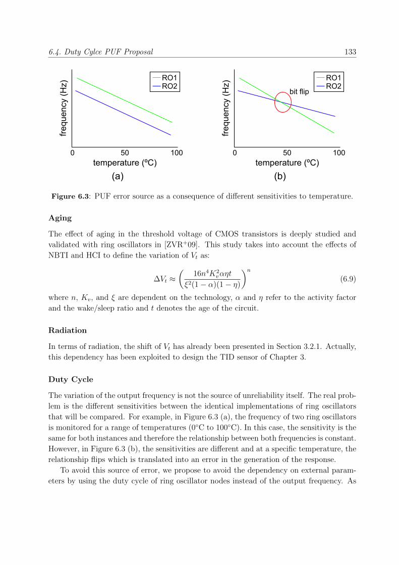
6.4. Duty Cylce PUF Proposal 133
temperature (ºC)0 50 100
freq
uen
cy (
Hz)
temperature (ºC)0 50 100
freq
uen
cy (
Hz)
bit flip
(a) (b)
RO1RO2
RO1RO2
Figure 6.3: PUF error source as a consequence of different sensitivities to temperature.
Aging
The effect of aging in the threshold voltage of CMOS transistors is deeply studied and
validated with ring oscillators in [ZVR+09]. This study takes into account the effects of
NBTI and HCI to define the variation of Vt as:
∆Vt ≈(
16n4K2vαηt
ξ2(1− α)(1− η)
)n(6.9)
where n, Kv, and ξ are dependent on the technology, α and η refer to the activity factor
and the wake/sleep ratio and t denotes the age of the circuit.
Radiation
In terms of radiation, the shift of Vt has already been presented in Section 3.2.1. Actually,
this dependency has been exploited to design the TID sensor of Chapter 3.
Duty Cycle
The variation of the output frequency is not the source of unreliability itself. The real prob-
lem is the different sensitivities between the identical implementations of ring oscillators
that will be compared. For example, in Figure 6.3 (a), the frequency of two ring oscillators
is monitored for a range of temperatures (0◦C to 100◦C). In this case, the sensitivity is the
same for both instances and therefore the relationship between both frequencies is constant.
However, in Figure 6.3 (b), the sensitivities are different and at a specific temperature, the
relationship flips which is translated into an error in the generation of the response.
To avoid this source of error, we propose to avoid the dependency on external param-
eters by using the duty cycle of ring oscillator nodes instead of the output frequency. As

134 6. Application of the Duty Cycle Ring Oscillator Model to Improve PUF Reliability
was concluded in Equation 5.27, the duty cycle for the internal nodes in a hard config-
uration of ring oscillators is only dependent on the size of the ring oscillator transistors.
Therefore, using a relative magnitude, such as the duty cycle, removes the dependency
on environmental variables and maintains the variability of process fabrication. For our
prototype, we will focus on the K-ratio implementation (defined in Section 5.3.1). The
duty cycle of that configuration was deduced as:
di =ϕN + i(1− ϕ)
(N + 1)(ϕ+ 1)(6.10)
where ϕ was defined as the asymmetry relationship between transistor sizes of pMOS and
nMOS transistors in odd and even nodes (Wpo = Wne = ϕWpe = ϕWno).
Once the sources of error have been removed, it is time to explore the potential of
using the duty cycle measurement for implementing a Duty Cycle PUF (DC-PUF) based
on K-ratio ring oscillators. The variability of this configuration has already been studied
in Section 5.4.3 with the results plotted in Figures 5.17 and 5.18 (reproduced in Figures 6.4
and 6.5). The variability characterization was carried out with a 40 nm commercial tech-
nology and Monte Carlo simulations. The simulations consist in 100 different samples
which include the particular technology variability models provided by the foundry. A
first group of results showed the impact of the ϕ value in a medium size (15 stages) ring
oscillator. The results of these tests are summarized in Figure 6.4 for ϕ = 1; 2; 4; 10. For ϕ
= 1 all transistors are designed with balanced stages as in the conventional ring oscillator
and as expected the value of the duty cycle at any node is around 50%. The rest of the
simulations showed that increasing ϕ makes the differences of internal node duty cycles
bigger. Then each node can be separated as an individual value with an independent duty
cycle measurement multiplying by N , the number of stages in a ring oscillator, the only
one measurement of the frequency output in a traditional ring oscillator. In the 15-stage
ring oscillator example, the value ϕ = 4 would be enough for separating each node duty
cycle values from the rest of nodes.
The next design parameter we analyzed is the impact of N in the duty cycle variation.
In this case of study, we fixed ϕ = 4 and we implemented different ring oscillators with
N = 3; 5; 15; 45. The results are plotted in Figure 6.5. The variability range decreases if
the number of stages increases but the maximum and minimum value of the duty cycle
nearly keep constant. Thus, for a given value of ϕ, the ring oscillator which would be more
affected by process variability is the minimum size (3 stages). On the contrary, a bigger
ring oscillator gives more potential distributions to be analyzed and included in the CRP
generation. Therefore, the DC-PUF is a valid candidate to implement a highly reliable
PUF with these characteristics:
• Greater ϕ makes easier the differentiation of nodes.
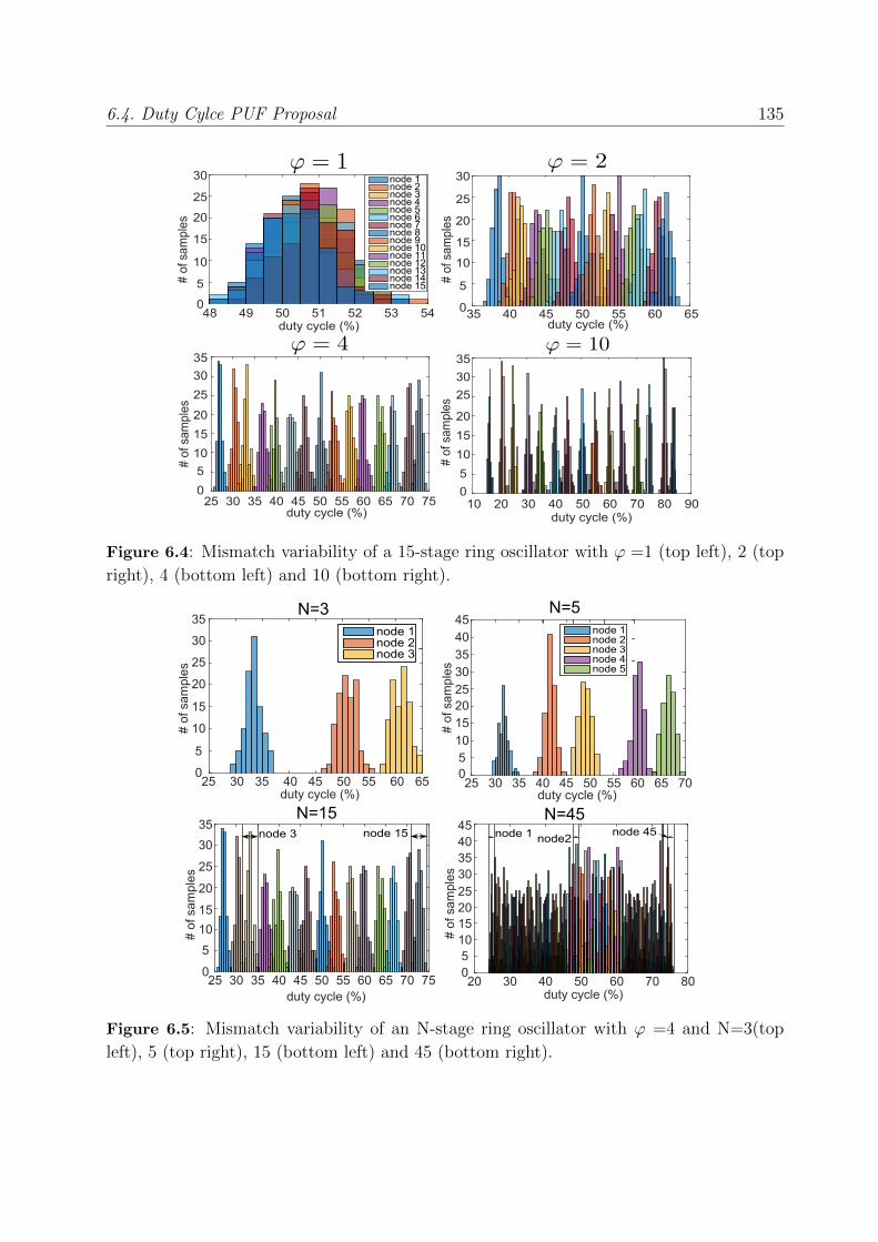
6.4. Duty Cylce PUF Proposal 135
duty cycle (%)48 49 50 51 52 53 54
# of
sam
ples
0
5
10
15
20
25
30 node 1node 2node 3node 4node 5node 6node 7node 8node 9node 10node 11node 12node 13node 14node 15
duty cycle (%)35 40 45 50 55 60 65
# of
sam
ples
0
5
10
15
20
25
30
duty cycle (%)25 30 35 40 45 50 55 60 65 70 75
# of
sam
ples
0
5
10
15
20
25
30
35
duty cycle (%)10 20 30 40 50 60 70 80 90
# of
sam
ples
0
5
10
15
20
25
30
35
Figure 6.4: Mismatch variability of a 15-stage ring oscillator with ϕ =1 (top left), 2 (top
right), 4 (bottom left) and 10 (bottom right).
duty cycle (%)25 30 35 40 45 50 55 60 65
# of
sam
ples
0
5
10
15
20
25
30
35node 1node 2node 3
duty cycle (%)25 30 35 40 45 50 55 60 65 70
# of
sam
ples
0510
152025
3035
4045
node 1node 2node 3node 4node 5
duty cycle (%)25 30 35 40 45 50 55 60 65 70 75
# of
sam
ples
0
5
10
15
20
25
30
35
duty cycle (%)20 30 40 50 60 70 80
# of
sam
ples
051015202530354045
N=15 N=45
N=5N=3
node 15node 3 node 45node 1 node2
Figure 6.5: Mismatch variability of an N-stage ring oscillator with ϕ =4 and N=3(top
left), 5 (top right), 15 (bottom left) and 45 (bottom right).

136 6. Application of the Duty Cycle Ring Oscillator Model to Improve PUF Reliability
Challenge (x)
RO 1
Enable
RO n
node 1
node N
Challenge (y)
Responsesenseamplifier
DC2V
DC2V
Figure 6.6: DC-PUF proposed architecture with (N,n) CRPs.
• Greater ϕ implies more area.
• Greater N decreases the variability of each node.
• Greater N increases the number of CRPs.
6.4.2 Architecture
The next step to exploit the duty cycle in a DC-PUF is the design of the PUF architecture.
We propose a variation of the conventional RO-PUF [SD07] that is depicted in Figure 6.6.
The elements that make the complete system are:
• An N decoder that enables a pair of ring oscillators to generate the response.
• n identical N -stage K-rate ring oscillators with ϕ 6= 1.
• n N -input multiplexers to select the internal node of ring oscillators.
• An N -to-2 demultiplexer to drive the output of ring oscillators to the response gen-
erator.
• Two Duty Cycle to Voltage Converters (DC2V) that generate a voltage dependent
on the input duty cycle.

6.4. Duty Cylce PUF Proposal 137
(a) (b)
Figure 6.7: Response generator blocks: a) DC2V converter [VAFK14], b) Sense ampli-
fier [WH11].
• A sense amplifier that clamps the bit response to one of the bias rails depending on
the relationship of the inputs.
The challenge of our PUF architecture is formed by a pair of values (x, y). x selects the
node of the ring oscillators that will be evaluated and therefore it is a value between 1 and
N . y is used to select the pair of ring oscillators whose nodes are selected, so it is a number
between 1 and n. Therefore the challenge consists of a word with a maximum limit of bits
of log2(N) + log2(n). The response of this particular implementation is a single bit like the
RO-PUF response.
The generation of the response is implemented with two different blocks. The first
block is a DC2V converter. This circuit is based on the proposed block in [VAFK14].
The schematic of the circuti is depicted Figure 6.7 (a). This circuit generates an output
proportional to the duty cycle of the input by charging and discharging the capacitances
C1 and C2. It works at three different stages. The first stage charges the capacitor C1
while the input signal is high. When it goes low, the charge stored in C1 is shared between
C1 and C2. And just before the next edge of the input C1 is discharged. After a few cycles,
the voltage stored at C2 stays steady and proportional to the duty cycle.
The last block is a sense amplifier. This block is based on a conventional sense amplifier
of Figure 6.7 (b) explained in [WH11]. This circuit drives the output to gnd or VDD
depending on which of the inputs is greater. Therefore, a minimum difference between the
output of both DC2V converters is amplified to generate the final bit response.
Hence our proposal requires more resources than the traditional RO-PUF but it multi-
plies the number of CRPs by up to N for the same number of ring oscillators, or it is able

138 6. Application of the Duty Cycle Ring Oscillator Model to Improve PUF Reliability
32 17-stage RO
32 17-stage RO
bit 1
32 17-stage RO
32 17-stage RO
bit 8
5 5
8 17-stage RO
8 17-stage RO
bit 1
8 17-stage RO
8 17-stage RO
bit 8
3 34
RO-PUF DC-PUF
Figure 6.8: Simulation Set-Up for the characterization of the RO-PUF and the DC-PUF.
to offer the same number of CRPs with a number of ring oscillator divided by up to N .
Therefore, both goals sought with the use of duty cycle instead of frequency (increasing
the CRP and improving the reliability) have proven being theoretically correct.
6.5 Simulation Results
The validation of the proposed DC-PUF was carried out with circuit simulations. These
simulations were made with the models of 40 nm commercial technology. First of all, we
will describe the system we simulated to generate the data set to validate our hypothesis.
The diagram of the tested PUFs is depicted in Figure 6.8. Two different PUFs have been
implemented in order to be able to compare a conventional RO-PUF to our new approach,
the DC-PUF.
Both types of PUF share the CRP morphology, the challenge is a 10 bit word and the
response is a 8 bit word. The generation of the responses is made by simulating 8 identical
PUF devices in parallel where each instance generates one bit. However the bits of the
challenges are used in a different way depending on the type of PUF. In the implemented
RO-PUF, the 10 input bits are divided into two different groups. The first 5 bits select the
first ring oscillator of a subset formed by half the ring oscillators. And the second group
of 5 bits selects the other ring oscillator within the other half of ring oscillators. Therefore
each subset of ring oscillators is made of 32 instances and the total PUF is made of 512
ring oscillators. All of them are implemented with a 17-stage ring oscillator.
On the other hand, the generation of the responses in the DC-PUF is slightly different.
The first 4 bits are used to select the node of each 17-stage ring oscillator asymmetrically
designed with ϕ = 4, while the other 6 bits work like the bits in the RO-PUF but with
subsets made of 8 ring oscillator instances. The result is that for the same number of CRPs,
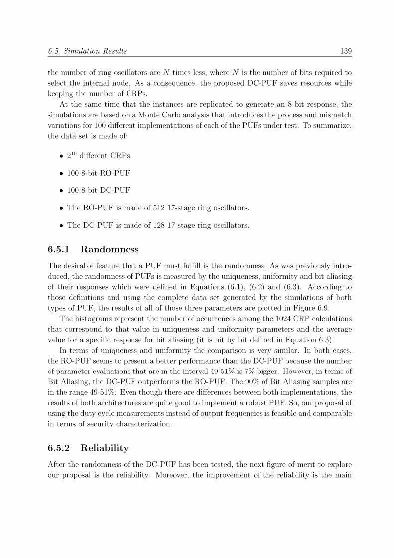
6.5. Simulation Results 139
the number of ring oscillators are N times less, where N is the number of bits required to
select the internal node. As a consequence, the proposed DC-PUF saves resources while
keeping the number of CRPs.
At the same time that the instances are replicated to generate an 8 bit response, the
simulations are based on a Monte Carlo analysis that introduces the process and mismatch
variations for 100 different implementations of each of the PUFs under test. To summarize,
the data set is made of:
• 210 different CRPs.
• 100 8-bit RO-PUF.
• 100 8-bit DC-PUF.
• The RO-PUF is made of 512 17-stage ring oscillators.
• The DC-PUF is made of 128 17-stage ring oscillators.
6.5.1 Randomness
The desirable feature that a PUF must fulfill is the randomness. As was previously intro-
duced, the randomness of PUFs is measured by the uniqueness, uniformity and bit aliasing
of their responses which were defined in Equations (6.1), (6.2) and (6.3). According to
those definitions and using the complete data set generated by the simulations of both
types of PUF, the results of all of those three parameters are plotted in Figure 6.9.
The histograms represent the number of occurrences among the 1024 CRP calculations
that correspond to that value in uniqueness and uniformity parameters and the average
value for a specific response for bit aliasing (it is bit by bit defined in Equation 6.3).
In terms of uniqueness and uniformity the comparison is very similar. In both cases,
the RO-PUF seems to present a better performance than the DC-PUF because the number
of parameter evaluations that are in the interval 49-51% is 7% bigger. However, in terms of
Bit Aliasing, the DC-PUF outperforms the RO-PUF. The 90% of Bit Aliasing samples are
in the range 49-51%. Even though there are differences between both implementations, the
results of both architectures are quite good to implement a robust PUF. So, our proposal of
using the duty cycle measurements instead of output frequencies is feasible and comparable
in terms of security characterization.
6.5.2 Reliability
After the randomness of the DC-PUF has been tested, the next figure of merit to explore
our proposal is the reliability. Moreover, the improvement of the reliability is the main

140 6. Application of the Duty Cycle Ring Oscillator Model to Improve PUF Reliability
Figure 6.9: Randomness of the RO-PUF and the DC-PUF implemented in simulations.
reason why we propose to change the traditional perspective of RO-PUF where the output
is based on measuring an absolute magnitude, to the DC-PUF where the response is
generated based on the relative magnitude of the duty cycle. As was analytically explained
in Section 6.4.1, this point is a priori feasible.
The simulations carried out are based on the same devices and architectures of RO-
PUF and DC-PUF used in the previous section but modifying the environmental variables
of temperature, bias voltage and radiation. These three variables were analyzed indepen-
dently, only one of them changes at a time while the other two stay at their nominal values.
In the case of our technology, the nominal bias voltage is 1.1 V, the nominal temperature
is 25 ◦C and the nominal radiation dose is 0 rad.
In order to clarify how the environmental variables are a source of unreliability for
PUFs, we are going to explain how the temperature simulations were made and how the
bit flips are produced. The temperature tests are summarized and simplified in Figure 6.10.
As was previously introduced, the data set is made of 100 identical instances of 1024 CRPs
whit 8-bit responses. This amount of data is impossible to be clearly represented in a single
figure, hence in Figure 6.10 only 10 ring oscillators are plotted to ease the visibility of the
effects.
First, in Figure 6.10 (a) the frequency of the ring oscillators is monitored for a tem-
perature range from -50 ◦C to 100 ◦C. In this figure, it is evident how for different imple-
mentations, the variability introduced by process is translated into different sensitivities of

6.5. Simulation Results 141
Figure 6.10: Temperature results of simulations carried out to characterize the reliability
of RO-PUFs and DC-PUFs.
frequency with respect to temperature. Figure 6.10 (b) is a zoom in the region of 30 ◦C
to 45 ◦C. In this figure, we can see how the instances RO-PUF6 and RO-PUF8 crossed. If
two lines are crossed, it means that the response generated with that pair of ring oscillators
will flip as was presented in Figure 6.3. Therefore, it will affect the reliability of the PUF.
Figures 6.10 (c) and (d) represent the duty cycle of 10 ring oscillators at nodes 3 and
11 respectively. As can be seen, for the same temperature variation, the variation of the
duty cycle is less than ±0.1% from the nominal value while the frequency varies more than
±4%. At the same time, the stability of this magnitude makes that there is only one flip of
lines among the 10 measurements of ring oscillators while with frequency, there are more.
Furthermore, there are no relationship between duty cycles at nodes 3 and 11, therefore
the duty cycle at different nodes does not imply any correlation from one node to another,
what would become less robust against side channel attacks.
The other two environmental variables are tested in the same way. The bias voltage is
simulated for a range of ±10% of the nominal value (1.1 V). And for the radiation dose,
the PUFs are simulated for a dose from 0 to 1 Mrad. The simulation of the radiation dose
has been carried out using the same technique that the used for the sensor in Chapter 3.
We have used the results of the characterization of a similar technology of 65 nm [BVA+12]

142 6. Application of the Duty Cycle Ring Oscillator Model to Improve PUF Reliability
Figure 6.11: Reliability of RO-PUF and DC-PUF for temperature, bias voltage and radi-
ation dose variation.
to shift the threshold voltage, Vt, and the leakage current of CMOS transistors.
The results of the three different types of reliability analysis are presented in Figure 6.11.
In these plots, at nominal conditions, the reliability is considered 100% due to the fact that
in simulations there is no option to make different measurements of the same conditions
with different results. However, in real implementations, this case can be less than 100%.
As can be seen, the DC-PUF outperforms the traditional RO-PUF in terms of reliability. In
all of the three different scenarios it is more robust against the variation of environmental
variables with an improvement of more than 20% at the worst case in radiation dose
simulation. According to the simulation results, it is clear that the improvement of using
a relative variable instead of an absolute one outperforms the reliability of the system for
the variation of environmental parameters.
6.5.3 Robustness
In terms of robustness, the DC-PUF proposal is similar to the traditional RO-PUF. As it
is a silicon and intrinsic PUF, both are good against passive, active and replace attacks.
However, the strong characteristic of the DC-PUF, with a much higher number of CRPs
makes that model attacks are much more difficult than the attacks to the RO-PUF. The
quantitative study of the robustness of our proposal will be carried out with the manufac-
tured proof of concept explained in the next Section.

6.6. Proof of concept 143
10 35-stage RO 4x10-input
mux
10-inputmux
out 210 125-stage RO 4x
out 1
out 310 251-stage RO 4x
out 410 125-stage RO 8x
out 510 125-stage RO 16x
Figure 6.12: Diagram of the implemented test architecture for DC-PUF exploration.
6.6 Proof of concept
Simulations have supported the use of duty cycle for the DC-PUF. To validate them, we
have fabricated a chip with a set of asymmetrical ring oscillators. It is a proof of concept
to explore the duty cycle characteristics and reliability in real circuits beyond the possible
inaccuracies and simplifications made by simulations. It has been implemented with the
same 40 nm technology used for simulations.
Instead of fabricating a complete DC-PUF, we have implemented independent ring
oscillators with different configurations to compare their performance and potential to be
included in the DC-PUF architecture proposed in Section 6.4.2. The test structure follows
the scheme of Figure 6.12. It is made of 50 different ring oscillators divided into 5 groups:
• 10 35-stage ring oscillators with ϕ = 4.
• 10 125-stage ring oscillators with ϕ = 4.
• 10 251-stage ring oscillators with ϕ = 4.
• 10 125-stage ring oscillators with ϕ = 8.
• 10 125-stage ring oscillators with ϕ = 16.
Each group of ring oscillators drives only one output. Therefore two stages of multi-
plexers have been designed. The first stage selects one node out of 10 possibilities and the
second stage selects one ring oscillator out of the 10 implemented. Therefore, the amount
of duty cycle measurements per chip is 500 (10 nodes x 10 ring oscillators x 5 groups).

144 6. Application of the Duty Cycle Ring Oscillator Model to Improve PUF Reliability
Figure 6.13: Layout of the fabricated proof of concept for the duty cycle exploration.
Figure 6.13 is the layout of the implemented test circuit. In this figure we can see the
distribution and the resources needed for each group of ring oscillators. With all data, the
goal is to analyze the randomness and the reliability of the duty cycle based PUF and to
compare these results against simulations.
So far, the implementation of the proof of concept has been fabricated. The next step
will be to completely characterize those designs. This process will be implemented following
the same scheme used for the characterization of the sensor presented in Section 3.4.3 and
the characterization of the SET tolerant ring oscillator in Section 4.7.1. The tests of the
DC-PUF will use the same measurement hardware (Xilinx FPGA board Virtex5 ML505,
the Agilent MSO9051 oscilloscope and a PC) than the previous tests. The breadboard and
test boards are different and adapted to the implemented 40 nm chip.
6.7 Conclusions
In this chapter we have presented a novel approach for a ring oscillator based Physically
Unclonable Function. First we have summarized the state of the art of these security prim-
itives by outlining the different types of PUFs and their characteristic. And we have also
introduced the most extended quality factors used for measuring and comparing different
PUF approaches. Then we have focused on RO-PUFs as one of the most mature and
developed architectures for implementing this type of systems.
So far, RO-PUFs have been a silicon, intrinsic and weak PUF that generates the re-
sponse using the output frequencies of ring oscillators. All the implementations are fo-
cused on measuring and comparing the frequencies. This approach has shown two main

6.8. Related Publications 145
disadvantages. The first one is the limited number of CRPs they use for generating their
”secret”. The second disadvantage is their decreasing reliability as a consequence of the
great dependency of ring oscillators frequency on the environmental parameters.
With our new design we address both problems. Our approach is based on the fully
configurable duty cycle ring oscillator modeled in Chapter 5. Particularly, we use the
hard configuration which configures the duty cycle of internal nodes by designing the
size of oscillator transistors individually. The reason to use the duty cycle instead of the
frequency is because it is a relative magnitude and it is intrinsically more robust against
environmental variations. Moreover, using the hard configuration, the number of possible
CRPs is multiplied by the number of stages of the implemented ring oscillators.
We have explored theoretically the characteristics of the duty cycle that makes our
proposal more robust against variations. Additionally to the conventional characterization
of PUF reliability against temperature, bias voltage and aging, we have proposed the
introduction of radiation absorbed dose as a non-negligible source of unreliability as a
consequence of the enhancement of radiation effects due to shrinking of the technology.
We have also simulated our proposed architecture with a 40 nm commercial technology.
These simulations have shown a good quality as PUFs and a great improvement in RO-
PUF reliability up to 20% in the worst case. We have finally fabricated a chip to validate
the proof of concept and the test plan is being designed and implementing for a future
characterization.
6.8 Related Publications
• J. Agustin and M. L. Lopez-Vallejo, ”A temperature-independent PUF with a config-
urable duty cycle of CMOS ring oscillators,” 2016 IEEE International Symposium on
Circuits and Systems (ISCAS), Montreal, QC, 2016, pp. 2471-2474. doi: 10.1109/IS-
CAS.2016.7539093


Chapter 7
Conclusions and Future Work
Chapter 7
Conclusions and Future Work
Modeling and Design of Ring Oscillators and their Application in Radiation Environments
is the title of this Thesis and it summarizes the topics addressed in it. As the title says, this
work has been focused on the convergence of two complementary subjects: ring oscillators
and radiation environments. First, we have generally introduced both themes: the effects
of radiation environments in electronics to understand the involved physical interaction,
and the structure of ring oscillators to understand their operation. The combination of
these two relevant topics has resulted in the original contributions of Chapters 3, 4, 5 and
6.
The first application of ring oscillators within radiation environments we have proposed
has dealt with the problem of Total Ionization Dose (TID) in electronic systems. This cu-
mulative effect shifts the nominal performance of electronic devices due to the modification
of charge distribution within the structure of semiconductors. Therefore, monitoring the
degradation of electronics plays a very important role in radiation applications to ensure
the reliability of systems. So far, the most extended devices to perform this task have been
the RADFETs. RADFETs have proven to be suitable for many applications but their main
drawback is that they only monitor the exposed dose instead of the real absorbed dose.
In order to implement a real absorbed dose sensor, we have proposed a new architecture
based on ring oscillators. The achievements of this work can be summarized as:
• Modeling and design of a smart sensor. The designed sensor is a self-timed design,
fully integrable, digital and with a configurable sensitivity. Its response has been
analytically modeled where the absorbed dose has been introduced in the model
through experimental results provided by a previous published work.
• Fabrication of the sensor. We have implemented and fabricated the TID sensor with
a commercial 0.35 µm technology. The implementation has divided the area of the
sensor into two different parts: the sensitive zone and the control. While the control
has used RHBD techniques to minimize the impact of dose in the measurements, the
sensitive zone is unhardened in order to maximize the absorption of radiation and
increase the sensitivity of the sensor.
• Radiation test and validation. A set of test have also been performed with a 60Co

149
source using the NAYADE facility at CIEMAT. This set of tests swept radiation
doses up to 575 krad with a dose rate of 26.51 krad/h. The test has validated the
developed model and the hypothesis of using a ring oscillator as the sensitive part of
a TID sensor.
• Temperature characterization. The impact of temperature has also been studied due
to its influence on our proposal reliability measurements. As a result, we proposed a
calibration system and we discussed the utilization of this ring oscillator based sensor
in a self-recovery system.
The second design of ring oscillators for radiation applications has addressed the har-
monic induced error. This error was introduced and characterized by Chen in [C+14]. It
is caused by SETs and it is potentially dangerous for every system that uses ring oscil-
lator in radiation environments. It causes a shift in the fundamental frequency of ring
oscillator up to higher odd harmonics. This change in operation could be translated into
a temporary error or even a SEFI. Our approach to solve these problems breaks with the
traditional view of ring oscillators which only considers the output frequency. In order to
avoid the harmonic induced error, we designed an asymmetrical ring oscillator whose duty
cycle is different from 50% to remove the vulnerability window. Within this topic the main
conclusions we draw are:
• We have modeled and designed a SET tolerant ring oscillator. This ring oscillator uses
a special design based on asymmetrical configurations of odd pull up and even pull
down networks with respect to even pull up and odd pull down. This methodology
electrically masks the SET-induced glitches within the ring oscillator loop.
• We have fabricated two types of test vehicle to validate our hypothesis and simu-
lations with a commercial 0.35 µm technology. Each vehicle is based on modifying
the pull up and pull down networks with different techniques. The first one uses the
size of transistors to make faster or slower networks while the second approach uses
voltage controlled current starved transistors to perform the same task.
• Both implementations have been validated against the Harmonic Induced Error. In-
stead of validating our proposal with expensive tests using a conventional source of
SETs (accelerometers, cyclotrones or pulsed lasers) we have implemented an emula-
tion SET system that infers the third harmonic to the ring oscillator.
• The design we have proposed to solve this particular problem is not only a solution
to it but it also opens a new perspective to exploit the duty cycle characteristic of
ring oscillators ignored so far.

150 7. Conclusions and Future Work
As an extension of the SET tolerant ring oscillator, we have extensively modeled the
duty cycle of ring oscillators. Previous works have been focused only on the frequency
of ring oscillators or on the figures of merit of these devices as oscillators (phase noise,
jitter, etc.) but none has analyzed their duty cycle. Moreover, systems that require clock
signals with configurable duty cycles or different from 50% leave this task to complementary
blocks. Opposite to those approaches, our work allows to implement a fully configurable
duty cycle ring oscillator without using any additional resource. The conclusions of the
developed model can be outlined as:
• We have set the analytical basis for understanding and designing a ring oscillator
whose outputs are clock signals with a duty cycle different from 50% and fully-
configurable. Our first analysis has revealed the design parameters that can be used
to configure the duty cycle.
• According to the revealed parameters, we have developed two different models that
agree with the two different implementations of the SET tolerant ring oscillator.
One uses different transistor sizes and the other is supported by using different bias
voltage schemes.
• The models have been simulated and validated with a commercial 40 nm technology.
Many different simulations have been carried out and all of them converge to our
model with a maximum deviation of 6% in the worst case and 2% for ring oscillators
with high number of stages.
• Additionally to the duty cycle model, we have analyzed two important features: the
variation of duty cycle due to PVT variations and the phase noise characteristics of
our design. Regarding PVT variations, the duty cycle has shown to be dependent on
the size of the ring oscillator and on the asymmetric ratio. The analysis of the phase
noise has proven to be consistent with the previous works about this subject applied
to the conventional ring oscillators.
Finally we have applied the model of the configurable duty cycle of ring oscillators to
a particular application, a Physically Unclonable Function (PUF). This application is
not specific of radiation environments, however, as the radiation effects are becoming a
concern even at ground level, it is important to consider them for critical applications such
as PUFs. As security hardware, the reliability of PUFs cannot be compromised by external
factors, but conventional RO-PUFs have not successfully overcome their effects. We have
designed and implemented a DC-PUF that outperforms the reliability of RO-PUFs. The
achievements we have reached so far with our DC-PUF are:
• We have analyzed the independence of duty cycle against external variations using
the developed model based on configuring the duty cycle by individually designing

151
the size of each transistor. This design has shown a high reliability against the worst
conditions improving the conventional PUF in more than 20%.
• We have introduced the analysis of radiation dose in the study of PUF reliability,
which has not been considered in PUF works so far.
• We have proposed an architecture for the DC-PUF that increments the number of
CRPs even for implementations with less resources. Moreover we have fabricated a
proof of concept of our proposal in a commercial 40 nm technology to validate our
hypothesis of using the duty cycle to improve the reliability of RO-PUFs.
As the main conclusion of this work, we have explored the performance of ring oscilla-
tors in radiation environments with the goals of improving their applications and pushing
forward their implementations. We have not only accomplished those tasks but we have
also developed a new model with the potential to improve the ring oscillator based appli-
cations at any circumstance.
Therefore, from the point of view of a circuit designer, we have covered all stages of a
design flow, from the modeling to the design, implementation, fabrication, measurement
and characterization. And our contributions to the state of the art have been also diverse
as the different publications show.
• In the field of modeling, we have proposed an original model of the duty cycle of
ring oscillators while the rest of works so far have been focused on the definition of
the output frequency. The big contribution of this model is the change of paradigm
for the use of ring oscillators. From now, the duty cycle is a new parameter to be
exploited in this kind of systems.
• In the field of design, we have made a SEE free ring oscillator design. This design
helps to solve a recently presented problem for ring oscillators in radiation environ-
ments and it contributes to solve the increasing problem of single event effects in
electronics as a consequence of the shrinking technology and increasing operation
frequency.
• In terms of implementation, we have improved the implementation of a security
hardware system. This contribution is not only restricted to the field of PUFs but it
is also applicable to any other implementation of ring oscillators where the reliability
against environmental variables is crucial.
• Regarding measurement and characterization, we have created a TID smart sensor
that actually measures the absorbed dose of electronics instead of the exposed dose
as the rest approaches. These data is important for self-recovery systems in radiation
environments as it allow to increase the lifetime of devices and their availability.

152 7. Conclusions and Future Work
7.1 Future Work
The work developed in this Thesis is the product of a high effort in research activity whose
results have been published in the international conferences and journals pointed out in
Section 1.4. We hope that the outputs of our work will inspire other researchers and that
our contributions will set the seed of new projects. We would like to put forward some ideas
that would continue with our work. We divide these lines depending on the advanced work
by this thesis and the estimated time for their development into short-term, medium-term
and long-term future works.
Short-Term
In the future short-term work we collect the immediate future work that is a direct exten-
sion from this work. Some of these works are:
• Implementation of the TID Smart Sensor in an FPGA device. As mentioned in
Chapter 3, the sensor is able to be integrated in all kind of electronic devices. The
implementation in an FPGA would generate a valuable information about the effect
of radiation in the counter and the pulse generator because in those devices, we will
not be able to implement the RHBD techniques we propose in this Thesis.
• Improvement of the ring oscillator duty cycle model. The discussion in Chapter 5 has
pointed out how the accuracy of the presented model could be improved by removing
some of the simplifications we made to develop the actual model presented in our
work.
• We have fabricated a proof of concept of the designed DC-PUF. The future work will
be the characterization of the PUF. These tests will be focused on the characterization
of the randomness, reliability and robustness. In terms on randomness, we will
perform a NIST statistical test suite for randomness [RSN+01]. The reliability will
take into account the three variables we have simulated in the thesis and we will add
the impact of aging in the reliability of PUFs. The aging tests will be performed by
an accelerated aging process with temperature and bias voltage stress. Regarding
robustness, we will try to foresee the response of PUFs by attacking our fabricated
devices with model attacks and power attacks.
Medium-Term
We categorize as medium-term future work those lines that require significant effort to
develop them but that they are not enough to generate a new research line.

7.1. Future Work 153
• Development of an automated tool to analyze the most TID sensitive areas of an
electronic chip and to place our integrated TID sensor within a TID monitor network.
This topic would be focused on two points. First, it will implement the self-recovery
system discussed Section 3.7. Second, the automated tool will be able to integrate
the monitor network in any design without adding effort to the design stage and in
an optimized topology for each particular implementation.
• Application of the asymmetrical pull down and pull up networks to combinational
logic paths to mitigate SETs in RTL designs. SETs are becoming the main concern of
radiation effects in modern technologies, therefore new approaches to mitigate them
will be necessary for future designs. The same mitigation technique that enhances the
removal of a SET in a ring oscillator could be used in a non-feedback combinational
path. Some constraints may be taken into account to implement this solution, such
as, maximum frequency of the system, critical path, minimum number of gates to
apply the measurements, etc.
• The duty cycle model has opened the possibility of changing the paradigm of ring
oscillators from frequency sources to duty cycle. This model can be applied to many
of the traditional applications based on ring oscillators, for example, True Random
Number Generators, Pulse Width Modulators or Time to Digital Converters. The
possibility of individually configuring the duty cycle of each node within a ring os-
cillator change makes possible the generation of new devices such as a Linearization
Readout System or a Configured Function Generator.
Long-Term
We refer as long-term future works those new research lines able to generate new full
projects.
• Impact of new technologies in the accuracy of gate delay and duty cycle ring oscillator
models. The last fabrication nodes are pushing the silicon based technologies to
the limit of physics. During the last decade, many different proposals have been
developed to replace the traditional silicon CMOS devices for new materials and
structures. For example, the first approach to continue with Moore’s law was the use
of FinFETs. Among the new alternative technologies would be the carbon nanotubes
transistors or different heterojunctions materials such as III-V semiconductors. In
these new proposals, the previous models of transistor current differ from actual
models, and their accuracy impact on the theoretical gate delay of each technology.
This parameter has fixed the maximum frequency of a particular technology since
the beginning of semiconductor industry. The accuracy of new technology models
154 7. Conclusions and Future Work
will also impact in the accuracy of our proposed model of ring oscillators and it must
be taken into account.
• Standardization of radiation hardening in the definition of standard libraries for com-
mercial technologies. The development of standard cell libraries supposed and huge
step in the evolution of semiconductor industry. It allowed the implementation of
extremely complex designs in a short time thanks to the automated tools that synthe-
size, place and route a particular solution. In this context, the open source Liberty
library modeling format is the semiconductor industry’s most widely supported li-
brary standard. In order to introduce the radiation variable in the automated design
flow, we propose the introduction of this process in the definition of the Liberty stan-
dard. With this approach, it would be possible an automated design process of a
design with a configurable radiation hardened level.
• Security hardware attacks inducing radiation effects. In this Thesis we have seen
how radiation modifies the reliability of PUFs. This weakness of PUFs can be ex-
trapolated to other security systems and it can also be useful to attack them. In
this line, radiation effects could be used to compromise the security of those systems.
For example, the TID effects could modify the challenge response pair of a particular
system to break the system or to replace an original system by a corrupt one. And
SEEs could individually control the value of a particular node if the impact of a
particle is completely controlled in time and area.
References
[A+06] Asad Abidi et al. Phase noise and jitter in CMOS ring oscillators. Solid-State Circuits, IEEE Journal of,
41(8):1803–1816, 2006.
[ADK99] S. K. Antiochos, C. R. DeVore, and J. A. Klimchuk. A Model for Solar Coronal Mass Ejections. The
Astrophysical Journal, 510(1):485, 1999.
[AG11] Karim Abdelhalim and Roman Genov. Cmos dac-sharing stimulator for neural recording and stimulation
arrays. In IEEE International Symposium on Circuits and Systems (ISCAS), 2011, pages 1712–1715. IEEE,
2011.
[AHG+13] J. R. Ahlbin, N. C. Hooten, M. J. Gadlage, J. H. Warner, S. P. Buchner, D. McMorrow, and L. W. Massengill.
Identification of pulse quenching enhanced layouts with subbandgap laser-induced single-event effects. In
Reliability Physics Symposium (IRPS), 2013 IEEE International, pages 6C.2.1–6C.2.6, April 2013.
[AHM03] Clive M Alabaster, Evan J Hughes, and John H Matthew. Medium prf radar prf selection using evolutionary
algorithms. 39(3):990–1001, 2003.
[ARH+15] L Artola, NJ-H Roche, G Hubert, A Al Youssef, A Khachatrian, P McMarr, and H Hughes. Analysis of
Angular Dependence of Single-Event Latchup Sensitivity for Heavy-Ion Irradiations of CMOS Technology.
IEEE Transactions on Nuclear Science, 62(6):2539–2546, 2015.
[Bar06] H.J. Barnaby. Total-Ionizing-Dose Effects in Modern CMOS Technologies. Nuclear Science, IEEE Transac-
tions on, 53(6):3103–3121, Dec 2006.
[Bau05a] R. C. Baumann. Radiation-induced soft errors in advanced semiconductor technologies. IEEE Transactions
on Device and Materials Reliability, 5(3):305–316, Sept 2005.
[Bau05b] Robert Baumann. Soft errors in advanced computer systems. IEEE Design & Test of Computers, 22(3):258–
266, 2005.
[BCF+11] G Bianchi, N Costantino, L Fanucci, J Incandela, G Magazzu, C Tongiani, and S Saponara. Radiation tolerant
IP Cores for the control and readout of Front-End electronics in High Energy Physics experiments. In Nuclear
Science Symposium and Medical Imaging Conference (NSS/MIC), 2011 IEEE, pages 2124–2127. IEEE, 2011.
[BD13] M Buchvarova and D Draganov. Cosmic-ray spectrum approximation model: experimental results and com-
parison with other models. Solar physics, 284(2):599–614, 2013.
[BEM+06] JM Benedetto, PH Eaton, DG Mavis, M Gadlage, and T Turflinger. Digital single event transient trends with
technology node scaling. IEEE Transactions on Nuclear Science, 53(6):3462–3465, 2006.

156 REFERENCES
[BG15] Marta Bagatin and Simone Gerardin. Ionizing Radiation Effects in Electronics: From Memories to Imagers,
volume 50. CRC Press, 2015.
[BK+14] Georg T Becker, Raghavan Kumar, et al. Active and Passive Side-Channel Attacks on Delay Based PUF
Designs. IACR Cryptology ePrint Archive, 2014:287, 2014.
[BM09] Musard Balliu and Isabella Mastroeni. A weakest precondition approach to active attacks analysis. In
Proceedings of the ACM SIGPLAN Fourth Workshop on Programming Languages and Analysis for Security,
pages 59–71. ACM, 2009.
[BMPM13] S. P. Buchner, F. Miller, V. Pouget, and D. P. McMorrow. Pulsed-laser testing for single-event effects inves-
tigations. IEEE Transactions on Nuclear Science, 60(3):1852–1875, June 2013.
[BNK98] L Bisdounis, S Nikolaidis, and O Koufopavlou. Analytical transient response and propagation delay evaluation
of the cmos inverter for short-channel devices. IEEE Journal of Solid-State Circuits, 33(2):302–306, 1998.
[BRW+15] D. A. Black, W. H. Robinson, I. Z. Wilcox, D. B. Limbrick, and J. D. Black. Modeling of single event transients
with dual double-exponential current sources: Implications for logic cell characterization. IEEE Transactions
on Nuclear Science, 62(4):1540–1549, Aug 2015.
[BS97] Eli Biham and Adi Shamir. Differential fault analysis of secret key cryptosystems. In Annual International
Cryptology Conference, pages 513–525. Springer, 1997.
[BSA+05] J. D. Black, A. L. Sternberg, M. L. Alles, A. F. Witulski, B. L. Bhuva, L. W. Massengill, J. M. Benedetto,
M. P. Baze, J. L. Wert, and M. G. Hubert. HBD layout isolation techniques for multiple node charge collection
mitigation. IEEE Transactions on Nuclear Science, 52(6):2536–2541, Dec 2005.
[BSH75] D Binder, EC Smith, and AB Holman. Satellite anomalies from galactic cosmic rays. IEEE Transactions on
Nuclear Science, 22(6):2675–2680, 1975.
[BVA+12] S Bonacini, P Valerio, R Avramidou, R Ballabriga, F Faccio, K Kloukinas, and A Marchioro. Characterization
of a commercial 65 nm CMOS technology for SLHC applications. Journal of Instrumentation, 7(01):P01015,
2012.
[BX08] Sebastien Bourdarie and Michael A Xapsos. The space radiation environment. 2008.
[C+14] Yongpin P Chen et al. Single-Event Transient Induced Harmonic Errors in Digitally Controlled Ring Oscilla-
tors. 61(6):3163–3170, Dec 2014.
[Cas10] Megan Colleen Casey. Single-event Effects in Digital CMOS Circuits Operating at Ultra-low Power. PhD
thesis, Vanderbilt University, Nashville, TN, 2010.
[CBDN14] Luca Cassano, Alberto Bosio, and Giorgio Di Natale. A novel adaptive fault tolerant flip-flop architecture
based on TMR. In 2014 19th IEEE European Test Symposium (ETS), pages 1–2. IEEE, 2014.
[CBN+09] Megan C Casey, Bharat L Bhuva, Sarah A Nation, Oluwole A Amusan, T Daniel Loveless, Lloyd W Massengill,
Dale McMorrow, and Joseph S Melinger. Single-event effects on ultra-low power CMOS circuits. In IEEE
International Reliability Physics Symposium, pages 194–198, Apr 2009.
[CCC+94] DL Chenette, J Chen, E Clayton, TG Guzik, JP Wefel, M Garcia-Munoz, C Lopate, KR Pyle, KP Ray,
EG Mullen, et al. The CRRES/SPACERAD heavy ion model of the environment (CHIME) for cosmic ray
and solar particle effects on electronic and biological systems in space. IEEE Transactions on Nuclear Science
(Institute of Electrical and Electronics Engineers);(United States), 41(CONF-940726–), 1994.
[CCS+14] J. S. Chang, K. S. Chong, W. Shu, T. Lin, J. Jiang, N. K. Z. Lwin, and Y. Kang. Radiation-hardened library
cell template and its total ionizing dose (TID) delay characterization in 65nm CMOS process. In 2014 IEEE
57th International Midwest Symposium on Circuits and Systems (MWSCAS), pages 821–824, Aug 2014.
[CCSP11] Poki Chen, Shou-Chih Chen, You-Sheng Shen, and You-Jyun Peng. All-Digital Time-Domain Smart Temper-
ature Sensor With an Inter-Batch Inaccuracy of After One-Point Calibration. Circuits and Systems I: Regular
Papers, IEEE Transactions on, 58(5):913–920, 2011.

REFERENCES 157
[CCTM16] Carlos Colodro-Conde and Rafael Toledo-Moreo. ”Improving the Implementation of EDAC Functions in
Radiation-Hardened FPGAs”, pages 189–200. Springer International Publishing, Cham, 2016.
[Che15] An Chen. Utilizing the variability of resistive random access memory to implement reconfigurable physical
unclonable functions. IEEE Electron Device Letters, 36(2):138–140, 2015.
[CLC09] Steven Chingyei Chung, S Lu, and Shengyong Chen. Nonlinear feedback system for an inverter-based ring
oscillator. In WSEAS International Conference. Proceedings. Mathematics and Computers in Science and
Engineering, number 8. World Scientific and Engineering Academy and Society, 2009.
[CLI+09] S. Carbonetto, J. Lipovetzky, M.G. Inza, E. Redin, and A Faigon. Ring oscillators response to irradiation
and application to dosimetry. In Micro-Nanoelectronics, Technology and Applications, 2009. EAMTA 2009.
Argentine School of, pages 1–4, Oct 2009.
[CLS15] Ying Cao, Paul Leroux, and Michiel Steyaert. Radiation Hardened by Design. In Radiation-Tolerant Delta-
Sigma Time-to-Digital Converters, pages 25–38. Springer, 2015.
[CLT+14] D. Cardoza, S. D. LaLumondiere, M. A. Tockstein, D. L. Brewe, N. P. Wells, R. Koga, K. M. Gaab, W. T.
Lotshaw, and S. C. Moss. Comparison of single event transients generated by short pulsed x-rays, lasers and
heavy ions. IEEE Transactions on Nuclear Science, 61(6):3154–3162, Dec 2014.
[CLZ12] Ralph K Cavin, Paolo Lugli, and Victor V Zhirnov. Science and engineering beyond Moore’s law. Proceedings
of the IEEE, 100(Special Centennial Issue):1720–1749, 2012.
[CM03] David Czajkowski and Merrick McCartha. Ultra low-power space computer leveraging embedded SEU miti-
gation. In Proc. IEEE Aerospace Conf, volume 5, pages 2315–2328, 2003.
[CNV96] T. Calin, M. Nicolaidis, and R. Velazco. Upset hardened memory design for submicron CMOS technology.
IEEE Transactions on Nuclear Science, 43(6):2874–2878, Dec 1996.
[Con94] E. E. Conrad. Radiation effects research in the 60’s. IEEE Transactions on Nuclear Science, 41(6):2648–2659,
Dec 1994.
[Cre13] J. D. Cressler. Radiation Effects in SiGe Technology. IEEE Transactions on Nuclear Science, 60(3):1992–2014,
June 2013.
[CRL+03] K. A. Clark, A. A. Ross, H. H. Loomis, T. R. Weatherford, D. J. Fouts, S. P. Buchner, and D. McMorrow.
Modeling single-event effects in a complex digital device. IEEE Transactions on Nuclear Science, 50(6):2069–
2080, Dec 2003.
[DCHB83] JAMES T Diehl, ROBERT F Cali, NORMAN R Hertzer, and EDWIN G Beven. Complications of abdominal
aortic reconstruction. An analysis of perioperative risk factors in 557 patients. Annals of surgery, 197(1):49,
1983.
[DGA14] Igor A Danilov, Maxim S Gorbunov, and Andrey A Antonov. SET tolerance of 65 nm CMOS majority voters:
a comparative study. IEEE Trans Nucl Sci, 61:1597–1602, 2014.
[DPMT+11] PO Lucas De Peslouan, Cedric Majek, Thierry Taris, Yann Deval, Didier Belot, and Jean-Baptiste Begueret.
A new frequency synthesizers stabilization method based on a mixed Phase Locked Loop and Delay Locked
Loop architecture. In Circuits and Systems (ISCAS), 2011 IEEE International Symposium on, pages 482–485.
IEEE, 2011.
[Dre89] Paul V Dressendorfer. Radiation effects on MOS devices and circuits. Ionizing Radiation Effects in MOS
Devices and Circuits, edited by TP Ma and Paul V. Dressendorfer, John Wiley & Sons, New York, pages
256–332, 1989.
[DS03] Stephen Docking and Manoj Sachdev. A method to derive an equation for the oscillation frequency of a ring
oscillator. IEEE Transactions on Circuits and Systems I: Fundamental Theory and Applications, 50(2):259–
264, 2003.
158 REFERENCES
[dSFdSR+13] L. N. de Souza Fino, M. A. Guazzelli da Silveira, C. Renaux, D. Flandre, and S. P. Gimenez. Total ionizing dose
effects on the digital performance of irradiated octo and conventional fully depleted soi mosfet. In Radiation
and Its Effects on Components and Systems (RADECS), 2013 14th European Conference on, pages 1–4, Sept
2013.
[DSH00] P. Dudek, S. Szczepanski, and J.V. Hatfield. A high-resolution CMOS time-to-digital converter utilizing a
Vernier delay line. Solid-State Circuits, IEEE Journal of, 35(2):240–247, Feb 2000.
[DSR+15] Jayita Das, Kevin Scott, Srinath Rajaram, Drew Burgett, and Sanjukta Bhanja. MRAM PUF: A novel
geometry based magnetic PUF with integrated CMOS. IEEE Transactions on Nanotechnology, 14(3):436–
443, 2015.
[DWB+07] S DasGupta, AF Witulski, BL Bhuva, ML Alles, RA Reed, OA Amusan, JR Ahlbin, RD Schrimpf, and
LW Massengill. Effect of well and substrate potential modulation on single event pulse shape in deep submicron
cmos. IEEE Transactions on Nuclear Science, 6(54):2407–2412, 2007.
[EAP+14] Michela Esposito, Thalis Anaxagoras, Tony Price, Spyros Manolopoulos, Philip Evans, Kevin Wells, Nigel
Allinson, et al. Ionizing and non Ionizing radiation damage in a large area CMOS active pixel sensor for
medical applications. IEEE Transactions on Nuclear Science, 2014.
[EGVFC+12] Luis Entrena, Mario Garcia-Valderas, Raul Fernandez-Cardenal, Almudena Lindoso, Marta Portela, and Celia
Lopez-Ongil. Soft error sensitivity evaluation of microprocessors by multilevel emulation-based fault injection.
61(3):313–322, Mar 2012.
[EHA+15] D. Englisch, M. Horstmann, S. Athanasiou, R. J. E. Jansen, and B. Glass. Measurement of set injected charge
from a californium-252 source in 340 nm straight and enclosed layout nmos and pmos transistors. In 2015
15th European Conference on Radiation and Its Effects on Components and Systems (RADECS), pages 1–4,
Sept 2015.
[ES08] AS Elwakil and KN Salama. Nonlinear models of some ring oscillators. In Circuits and Systems and TAISA
Conference, 2008. NEWCAS-TAISA 2008. 2008 Joint 6th International IEEE Northeast Workshop on, pages
217–220. IEEE, 2008.
[ESK+15] O. Elhadidy, S. Shakib, K. Krenek, S. Palermo, and K. Entesari. A Wide-Band Fully-Integrated CMOS Ring-
Oscillator PLL-Based Complex Dielectric Spectroscopy System. Circuits and Systems I: Regular Papers,
IEEE Transactions on, 62(8):1940–1949, Aug 2015.
[EU04] Yalcin Alper Eken and John P Uyemura. A 5.9-GHz voltage-controlled ring oscillator in 0.18-µm CMOS.
Solid-State Circuits, IEEE Journal of, 39(1):230–233, 2004.
[FCMG13] V. Ferlet-Cavrois, L. W. Massengill, and P. Gouker. Single event transients in digital cmos;a review. IEEE
Transactions on Nuclear Science, 60(3):1767–1790, June 2013.
[FCPM+07] V. Ferlet-Cavrois, P. Paillet, D. McMorrow, N. Fel, J. Baggio, S. Girard, O. Duhamel, J. S. Melinger, M. Gail-
lardin, J. R. Schwank, P. E. Dodd, M. R. Shaneyfelt, and J. A. Felix. New insights into single event transient
propagation in chains of inverters;evidence for propagation-induced pulse broadening. IEEE Transactions on
Nuclear Science, 54(6):2338–2346, Dec 2007.
[FSF+11] K. Fruhashi, M. Shiozaki, A. Fukushima, T. Murayama, and T. Fujino. The arbiter-PUF with high uniqueness
utilizing novel arbiter circuit with Delay-Time Measurement. In Circuits and Systems (ISCAS), 2011 IEEE
International Symposium on, pages 2325–2328, May 2011.
[FSWG93] J Feynman, G Spitale, J Wang, and S Gabriel. Interplanetary proton fluence model: JPL 1991. Journal of
Geophysical Research: Space Physics, 98(A8):13281–13294, 1993.
[GAN+10] M. J. Gadlage, J. R. Ahlbin, B. Narasimham, B. L. Bhuva, L. W. Massengill, R. A. Reed, R. D. Schrimpf,
and G. Vizkelethy. Scaling trends in set pulse widths in sub-100 nm bulk cmos processes. IEEE Transactions
on Nuclear Science, 57(6):3336–3341, Dec 2010.
REFERENCES 159
[GAS10] Xiaoqing Ge, Murat Arcak, and Khaled N Salama. Nonlinear analysis of ring oscillator and cross-coupled
oscillator circuits. Dynamics of Continuous, Discrete and Impulsive Systems Series B: Applications and
Algorithms, 2010.
[GCvDD02] Blaise Gassend, Dwaine Clarke, Marten van Dijk, and Srinivas Devadas. Silicon Physical Random Functions.
In Proceedings of the 9th ACM Conference on Computer and Communications Security, CCS ’02, pages
148–160, New York, NY, USA, 2002. ACM.
[GK14] A. Garg and T.T. Kim. Design of SRAM PUF with improved uniformity and reliability utilizing device aging
effect. In Circuits and Systems (ISCAS), 2014 IEEE International Symposium on, pages 1941–1944, June
2014.
[GKT+14] P. Goncalves, A Keating, A Trindade, P. Rodrigues, M. Ferreira, P. Assis, M. Muschitiello, B. Nickson, and
C. Poivey. Modeling the response of the ESAPMOS4 RADFETs for the ALPHASAT CTTB experiment.
Nuclear Science, IEEE Transactions on, 61(3):1439–1443, June 2014.
[GMG+15] M. Gaillardin, M. Martinez, S. Girard, V. Goiffon, P. Paillet, J. L. Leray, P. Magnan, Y. Ouerdane, A. Bouken-
ter, C. Marcandella, O. Duhamel, M. Raine, N. Richard, F. Andrieu, S. Barraud, and O. Faynot. High Total
Ionizing Dose and Temperature Effects on Micro- and Nano-Electronic Devices. IEEE Transactions on Nuclear
Science, 62(3):1226–1232, June 2015.
[GMP+13] JO Goldsten, RH Maurer, PN Peplowski, AG Holmes-Siedle, CC Herrmann, and BH Mauk. The engineering
radiation monitor for the radiation belt storm probes mission. Space Science Reviews, 179(1-4):485–502, 2013.
[GMW08] Jody W Gambles, GK Maki, and SR Whitaker. Radiation hardening by design. International Journal of
Electronics, 95(1):11–26, 2008.
[GN14] Dinesh Ganta and Leyla Nazhandali. Study of IC aging on ring oscillator physical unclonable functions. In
Fifteenth International Symposium on Quality Electronic Design, pages 461–466. IEEE, 2014.
[GOB13] Massoud M Ghahroodi, Emre Ozer, and David Bull. SEU and SET-tolerant ARM Cortex-R4 CPU for
space and avionics applications. In Workshop on Manufacturable and Dependable Multicore Architectures at
Nanoscale, 2013.
[GOS15] S Golge, PM O’Neill, and TC Slaba. NASA Galactic Cosmic Radiation Environment Model: Badhwar-O’Neill
(2014). 2015.
[GPM00] A Giraldo, A Paccagnella, and A Minzoni. Aspect ratio calculation in n-channel MOSFETs with a gate-
enclosed layout. Solid-State Electronics, 44(6):981–989, 2000.
[GRD+16] M. J. Gadlage, A. H. Roach, A. R. Duncan, M. R. Halstead, M. J. Kay, P. Gadfort, J. R. Alhbin, and S. Stans-
berry. Alpha-particle and neutron-induced single-event transient measurements in subthreshold circuits. In
2016 IEEE International Reliability Physics Symposium (IRPS), pages SE–1–1–SE–1–6, April 2016.
[GRP+13] M. Gaillardin, M. Raine, P. Paillet, M. Martinez, C. Marcandella, S. Girard, O. Duhamel, N. Richard,
F. Andrieu, S. Barraud, and O. Faynot. Radiation effects in advanced SOI devices: New insights into Total
Ionizing Dose and Single-Event Effects. In 2013 IEEE SOI-3D-Subthreshold Microelectronics Technology
Unified Conference (S3S), pages 1–2, Oct 2013.
[GSC11] R. Graczyk, M. Stolarski, and P. Cormery. Exploratory study about the use of new reconfigurable FPGAs
in space. In Adaptive Hardware and Systems (AHS), 2011 NASA/ESA Conference on, pages 220–226, June
2011.
[HA13] G. Hubert and L. Artola. Single-event transient modeling in a 65-nm bulk cmos technology based on multi-
physical approach and electrical simulations. IEEE Transactions on Nuclear Science, 60(6):4421–4429, Dec
2013.
[HALV11] Ignacio Herrera-Alzu and Marisa Lopez-Vallejo. Self-reference scrubber for TMR systems based on xilinx
virtex FPGAs. In International Workshop on Power and Timing Modeling, Optimization and Simulation,
pages 133–142. Springer, 2011.

160 REFERENCES
[HALV13] Ignacio Herrera-Alzu and Marisa Lopez-Vallejo. Design techniques for Xilinx Virtex FPGA configuration
memory scrubbers. IEEE Transactions on Nuclear Science, 60(1):376–385, 2013.
[HAR15] G Hubert, L Artola, and D Regis. Impact of scaling on the soft error sensitivity of bulk, FDSOI and FinFET
technologies due to atmospheric radiation. Integration, the VLSI journal, 50:39–47, 2015.
[HG64] Harold L Hughes and Ronald R Giroux. Space Radiation Affects MOS FET’s. Electronics (US), 37(32), 1964.
[HKK+13] Sewook Hwang, Jabeom Koo, Kisoo Kim, Hokyu Lee, and Chulwoo Kim. A 0.008 500/spl mu/W 469 kS/s
Frequency-to-Digital Converter Based CMOS Temperature Sensor With Process Variation Compensation.
Circuits and Systems I: Regular Papers, IEEE Transactions on, 60(9):2241–2248, 2013.
[HKM16] J. W. Han, M. Kebaili, and M. Meyyappan. System on microheater for on-chip annealing of defects generated
by hot-carrier injection, bias temperature instability, and ionizing radiation. IEEE Electron Device Letters,
PP(99):1–1, 2016.
[HOT98] Akio Hirata, Hidetoshi Onodera, and K Tamura. Estimation of propagation delay considering short-circuit
current for static cmos gates. IEEE Transactions on Circuits and Systems I: Fundamental theory and appli-
cations, 45(11):1194–1198, 1998.
[HS74] Andrew Holmes-Siedle. The space-charge dosimeter: General principles of a new method of radiation detection.
Nuclear Instruments and Methods, 121(1):169–179, 1974.
[HS00] P. Hazucha and C. Svensson. Impact of CMOS technology scaling on the atmospheric neutron soft error rate.
IEEE Transactions on Nuclear Science, 47(6):2586–2594, Dec 2000.
[HSGMP14] A. G. Holmes-Siedle, J. O. Goldsten, R. H. Maurer, and P. N. Peplowski. RadFET Dosimeters in the Belt:
the Van Allen Probes on Day 365. IEEE Transactions on Nuclear Science, 61(2):948–954, April 2014.
[HSRG07] Andrew Holmes-Siedle, Federio Ravotti, and Maurice Glaser. The dosimetric performance of RADFETs in
radiation test beams. In Radiation Effects Data Workshop, 2007 IEEE, pages 42–57. IEEE, 2007.
[HTG89] KJ Hass, RK Treece, and AE Giddings. A radiation-hardened 16/32-bit microprocessor. IEEE Transactions
on Nuclear Science, 36(6):2252–2257, 1989.
[HYKD14] Charles Herder, Meng-Day Yu, Farinaz Koushanfar, and Srinivas Devadas. Physical unclonable functions and
applications: A tutorial. Proceedings of the IEEE, 102(8):1126–1141, 2014.
[IA15] F. Irom and S. G. Agarwal. Compendium of Single-Event Latchup and Total Ionizing Dose Test Results of
Commercial Digital to Analog Converters. In Radiation Effects Data Workshop (REDW), 2015 IEEE, pages
1–8, July 2015.
[IALV08] P. Ituero, J.L. Ayala, and M. Lopez-Vallejo. A Nanowatt Smart Temperature Sensor for Dynamic Thermal
Management. Sensors Journal, IEEE, 8(12):2036–2043, Dec 2008.
[ILVMO12] Pablo Ituero, Marisa Lopez-Vallejo, MAS Marcos, and Carlos Gomez Osuna. Light-weight on-chip monitoring
network for dynamic adaptation and calibration. Sensors Journal, IEEE, 12(6):1736–1745, 2012.
[Ind] Votsch Industrietechnik. VTL and VCL for temperature and climatic tests. [Online]. Available: http://v-
it.com.
[JCG+12] Adam Jacobs, Grzegorz Cieslewski, Alan D. George, Ann Gordon-Ross, and Herman Lam. Reconfigurable
Fault Tolerance: A Comprehensive Framework for Reliable and Adaptive FPGA-Based Space Computing.
ACM Trans. Reconfigurable Technol. Syst., 5(4):21:1–21:30, December 2012.
[JOH+15] W. R. Johnston, T. P. O’Brien, S. L. Huston, T. B. Guild, and G. P. Ginet. Recent Updates to the
AE9/AP9/SPM Radiation Belt and Space Plasma Specification Model. IEEE Transactions on Nuclear Sci-
ence, 62(6):2760–2766, Dec 2015.

REFERENCES 161
[JSS10] G Jovanovic, M Stojcev, and Zoran Stamenkovic. A CMOS voltage controlled ring oscillator with improved
frequency stability. Scientific Publications of the State University of Novi Pazar, Series A: Applied Mathe-
matics, Informatics and mechanics, 2(1):1–9, 2010.
[KAKAK03] Adnan Kabbani, Dhamin Al-Khalili, and Asim J Al-Khalili. Technology-portable analytical model for dsm
cmos inverter transition-time estimation. IEEE Transactions on Computer-Aided Design of Integrated Circuits
and Systems, 22(9):1177–1187, 2003.
[KC06] Jonathan E Knudsen and Lawrence T Clark. An area and power efficient radiation hardened by design flip-flop.
Nuclear Science, IEEE Transactions on, 53(6):3392–3399, 2006.
[KGM+08] Sandeep S Kumar, Jorge Guajardo, Roel Maes, Geert-Jan Schrijen, and Pim Tuyls. The butterfly PUF pro-
tecting IP on every FPGA. In Hardware-Oriented Security and Trust, 2008. HOST 2008. IEEE International
Workshop on, pages 67–70. IEEE, 2008.
[KHZS07] Aman Kansal, Jason Hsu, Sadaf Zahedi, and Mani B Srivastava. Power management in energy harvesting
sensor networks. ACM Transactions on Embedded Computing Systems (TECS), 6(4):32, 2007.
[KLA96] A Kelleher, W. Lane, and Leonard Adams. Investigation of on-chip high temperature annealing of PMOS
dosimeters. Nuclear Science, IEEE Transactions on, 43(3):997–1001, Jun 1996.
[KLR+11] Jae-Joon Kim, Barry P Linder, Rahul M Rao, Tae-Hyoung Kim, Pong-Fei Lu, Keith Jenkins, Chris H Kim,
Aditya Bansal, Saibal Mukhopadhyay, Ching-Te Chuang, et al. Reliability monitoring ring oscillator structures
for isolated/combined NBTI and PBTI measurement in high-k metal gate technologies. In Reliability Physics
Symposium (IRPS), 2011 IEEE International, pages 2B–4. IEEE, 2011.
[KPCC97] R Koga, SH Penzin, KB Crawford, and WR Crain. Single event functional interrupt (SEFI) sensitivity in
microcircuits. In Radiation and Its Effects on Components and Systems, 1997. RADECS 97. Fourth European
Conference on, pages 311–318. IEEE, 1997.
[KPnS15] Merlin Kole, Mark Pearce, and Maria Mu noz Salinas. A model of the cosmic ray induced atmospheric neutron
environment. Astroparticle Physics, 62:230 – 240, 2015.
[KT03] Kenneth R Knowles and Nandor G Thoma. Ring oscillator providing single event transient immunity, Novem-
ber 4 2003. US Patent 6,642,802.
[Lac08] Ronald C Lacoe. Improving integrated circuit performance through the application of hardness-by-design
methodology. IEEE transactions on Nuclear Science, 55(4):1903–1925, 2008.
[LCS+16] T. Lin, K. S. Chong, W. Shu, N. K. Z. Lwin, J. Jiang, and J. S. Chang. Experimental investigation into
radiation-hardening-by-design (RHBD) flip-flop designs in a 65nm CMOS process. In 2016 IEEE International
Symposium on Circuits and Systems (ISCAS), pages 966–969, May 2016.
[LKJ+12] T. D. Loveless, J. S. Kauppila, S. Jagannathan, D. R. Ball, J. D. Rowe, N. J. Gaspard, N. M. Atkinson,
R. W. Blaine, T. R. Reece, J. R. Ahlbin, T. D. Haeffner, M. L. Alles, W. T. Holman, B. L. Bhuva, and L. W.
Massengill. On-chip measurement of single-event transients in a 45 nm silicon-on-insulator technology. IEEE
Transactions on Nuclear Science, 59(6):2748–2755, Dec 2012.
[LKL97] Seog-Jun Lee, Beomsup Kim, and Kwyro Lee. A novel high-speed ring oscillator for multiphase clock gener-
ation using negative skewed delay scheme. IEEE Journal of Solid-State Circuits, 32(2):289–291, Feb 1997.
[LLZH16] Yang Liu, Lin Liu, Yuchen Zhou, and Shiyan Hu. Leveraging carbon nanotube technologies in developing
Physically Unclonable Function for cyber-physical system authentication. In Computer Communications
Workshops (INFOCOM WKSHPS), 2016 IEEE Conference on, pages 176–180. IEEE, 2016.
[LOM+98] R. C. Lacoe, J. V. Osborn, D. C. Mayer, S. Brown, and D. R. Hunt. Total-dose radiation tolerance of a
commercial 0.35 mu;m CMOS process. In Radiation Effects Data Workshop, 1998. IEEE, pages 104–110, Jul
1998.
162 REFERENCES
[LOM+01] RC Lacoe, JV Osborn, DC Mayer, S Brown, and J Gambles. Total-dose tolerance of the commercial tai-
wan semiconductor manufacturing company (TSMC) 0.35-µm CMOS process. In Radiation Effects Data
Workshop, 2001 IEEE, pages 72–76. IEEE, 2001.
[May90] Donald C Mayer. Modes of operation and radiation sensitivity of ultrathin SOI transistors. IEEE Transactions
on Electron Devices, 37(5):1280–1288, 1990.
[MBH+07] M. McLain, H. J. Barnaby, K. E. Holbert, R. D. Schrimpf, H. Shah, A. Amort, M. Baze, and J. Wert.
Enhanced TID Susceptibility in Sub-100 nm Bulk CMOS I/O Transistors and Circuits. IEEE Transactions
on Nuclear Science, 54(6):2210–2217, Dec 2007.
[McL88] F Barry McLean. Generic impulse response function for MOS systems and its application to linear response
analysis. IEEE Transactions on Nuclear Science, 35(6):1178–1185, 1988.
[MDA+12] M Meguellati, F Djeffal, D Arar, F Douak, and L Khettache. New RADFET dosimeter design for radioactive
environment monitoring applications. tC, 10:4, 2012.
[MDE97] Jean-Paul Meyer, Luke O’C Drury, and Donald C Ellison. Galactic cosmic rays from supernova remnants.
I. A cosmic-ray composition controlled by volatility and mass-to-charge ratio. The Astrophysical Journal,
487(1):182, 1997.
[MF10] BH Mauk and NJ Fox. Electron radiation belts of the solar system. Journal of Geophysical Research: Space
Physics, 115(A12), 2010.
[MGJ+13] N. N. Mahatme, N. J. Gaspard, S. Jagannathan, T. D. Loveless, B. L. Bhuva, W. H. Robinson, L. W.
Massengill, S. J. Wen, and R. Wong. Impact of supply voltage and frequency on the soft error rate of logic
circuits. IEEE Transactions on Nuclear Science, 60(6):4200–4206, Dec 2013.
[MGS13] Abhranil Maiti, Vikash Gunreddy, and Patrick Schaumont. A systematic method to evaluate and compare
the performance of physical unclonable functions. In Embedded systems design with FPGAs, pages 245–267.
Springer, 2013.
[MKS12] A. Maiti, I. Kim, and P. Schaumont. A Robust Physical Unclonable Function With Enhanced Challenge-
Response Set. IEEE Transactions on Information Forensics and Security, 7(1):333–345, Feb 2012.
[MKY+13] Masaki Masuda, Kanto Kubota, Ryosuke Yamamoto, Jun Furuta, Kazutoshi Kobayashi, and Hidetoshi On-
odera. A 65 nm low-power adaptive-coupling redundant flip-flop. IEEE Transactions on Nuclear Science,
60(4):2750–2755, 2013.
[MM15] H Mondal and MK Mandal. PLL-based clock recovery circuit using ring oscillator. International Journal of
Electronics Letters, pages 1–6, 2015.
[MMCK10] B. I. Matush, T. J. Mozdzen, L. T. Clark, and J. E. Knudsen. Area-Efficient Temporally Hardened by Design
Flip-Flop Circuits. IEEE Transactions on Nuclear Science, 57(6):3588–3595, Dec 2010.
[MO87] F Barry McLean and Timothy R Oldham. Basic mechanisms of radiation effects in electronic materials and
devices. Technical report, DTIC Document, 1987.
[MRFA15] Anas Mazady, Md Tauhidur Rahman, Domenic Forte, and Mehdi Anwar. Memristor puf-a security primitive:
Theory and experiment. IEEE Journal on Emerging and Selected Topics in Circuits and Systems, 5(2):222–
229, 2015.
[MRMK13] Ahmed Mahmoud, Ulrich Ruhrmair, Mehrdad Majzoobi, and Farinaz Koushanfar. Combined Modeling and
Side Channel Attacks on Strong PUFs. IACR Cryptology ePrint Archive, 2013:632, 2013.
[MRV+12a] R. Maes, V. Rozic, I. Verbauwhede, P. Koeberl, E. van der Sluis, and V. van der Leest. Experimental evaluation
of physically unclonable functions in 65 nm cmos. In ESSCIRC (ESSCIRC), 2012 Proceedings of the, pages
486–489, Sept 2012.

REFERENCES 163
[MRV+12b] R. Maes, V. Rozic, I. Verbauwhede, P. Koeberl, E. van der Sluis, and V. van der Leest. Experimental
evaluation of Physically Unclonable Functions in 65 nm CMOS. In ESSCIRC (ESSCIRC), 2012 Proceedings
of the, pages 486–489, Sept 2012.
[MS09] A. Maiti and P. Schaumont. Improving the quality of a Physical Unclonable Function using configurable Ring
Oscillators. In Field Programmable Logic and Applications, 2009. FPL 2009. International Conference on,
pages 703–707, Aug 2009.
[MS10] MK Mandal and BC Sarkar. Ring oscillators: Characteristics and applications. Indian journal of pure &
applied physics, 48:136–145, 2010.
[MS11] Abhranil Maiti and Patrick Schaumont. Improved ring oscillator PUF: an FPGA-friendly secure primitive.
Journal of cryptology, 24(2):375–397, 2011.
[MS14] Abhranil Maiti and Patrick Schaumont. The impact of aging on a physical unclonable function. IEEE
Transactions on Very Large Scale Integration (VLSI) Systems, 22(9):1854–1864, 2014.
[MSHL01] Ronald L Moore, Alphonse C Sterling, Hugh S Hudson, and James R Lemen. Onset of the magnetic explosion
in solar flares and coronal mass ejections. The Astrophysical Journal, 552(2):833, 2001.
[MSP+13] A Masi, G Spiezia, P Peronnard, M Donze, M Brugger, and R Losito. The new generation of the CERN
accelerator radiation monitoring system for electronics. Nuclear Science, IEEE Transactions on, 60(5):3475–
3482, 2013.
[MSSS11] Dominik Merli, Dieter Schuster, Frederic Stumpf, and Georg Sigl. Side-channel analysis of PUFs and fuzzy
extractors. In International Conference on Trust and Trustworthy Computing, pages 33–47. Springer, 2011.
[MT08] L. W. Massengill and P. W. Tuinenga. Single-Event Transient Pulse Propagation in Digital CMOS. IEEE
Transactions on Nuclear Science, 55(6):2861–2871, Dec 2008.
[MTV09] Roel Maes, Pim Tuyls, and Ingrid Verbauwhede. Low-overhead implementation of a soft decision helper data
algorithm for SRAM PUFs. In Cryptographic Hardware and Embedded Systems-CHES 2009, pages 332–347.
Springer, 2009.
[MW78] T. C. May and M. H. Woods. A New Physical Mechanism for Soft Errors in Dynamic Memories. In Reliability
Physics Symposium, 1978. 16th Annual, pages 33–40, April 1978.
[Nar08] Balaji Narasimham. Characterization of heavy-ion, neutron and alpha particle-induced single-event transient
pulse widths in advanced CMOS technologies. PhD thesis, Vanderbilt University, 2008.
[NBS+07] B. Narasimham, B. L. Bhuva, R. D. Schrimpf, L. W. Massengill, M. J. Gadlage, O. A. Amusan, W. T.
Holman, A. F. Witulski, W. H. Robinson, J. D. Black, J. M. Benedetto, and P. H. Eaton. Characterization of
Digital Single Event Transient Pulse-Widths in 130-nm and 90-nm CMOS Technologies. IEEE Transactions
on Nuclear Science, 54(6):2506–2511, Dec 2007.
[NBTA04] Nathan Nowlin, John Bailey, Bob Turfler, and Dave Alexander. A total-dose hardening-by-design approach
for high-speed mixed-signal CMOS integrated circuits. International journal of high speed electronics and
systems, 14(02):367–378, 2004.
[NSHB13] Dmitry Nedospasov, Jean-Pierre Seifert, Clemens Helfmeier, and Christian Boit. Invasive PUF analysis. In
Fault Diagnosis and Tolerance in Cryptography (FDTC), 2013 Workshop on, pages 30–38. IEEE, 2013.
[Nym06] R Nymmik. Initial conditions for radiation analysis: Models of galactic cosmic rays and solar particle events.
Advances in Space Research, 38(6):1182–1190, 2006.
[NZS+15] K. Ni, E. X. Zhang, I. K. Samsel, R. D. Schrimpf, R. A. Reed, D. M. Fleetwood, A. L. Sternberg, M. W.
McCurdy, S. Ren, T. P. Ma, L. Dong, J. Y. Zhang, and P. D. Ye. Charge Collection Mechanisms in GaAs
MOSFETs. IEEE Transactions on Nuclear Science, 62(6):2752–2759, Dec 2015.
164 REFERENCES
[OILV13] Carlos Gomez Osuna, Pablo Ituero, and Marisa Lopez-Vallejo. A Self-Timed Multipurpose Delay Sensor for
Field Programmable Gate Arrays (FPGAs). Sensors, 14(1):129–143, 2013.
[OLMY98] JV Osborn, RC Lacoe, DC Mayer, and G Yabiku. Total dose hardness of three commercial CMOS microelec-
tronics foundries. IEEE Transactions on Nuclear Science, 45(3):1458–1463, 1998.
[OM03a] Timothy R Oldham and FB McLean. Total ionizing dose effects in MOS oxides and devices. 2003.
[OM03b] T.R. Oldham and F.B. McLean. Total ionizing dose effects in MOS oxides and devices. Nuclear Science,
IEEE Transactions on, 50(3):483–499, June 2003.
[PAH14] L. Palkuti, M. Alles, and H. Hughes. The role of radiation effects in SOI technology development. In 2014
SOI-3D-Subthreshold Microelectronics Technology Unified Conference (S3S), pages 1–2, Oct 2014.
[PBS+16] Roberta Pilia, Guillaume Bascoul, Kevin Sanchez, Giovanna Mura, and Fulvio Infante. Single event transient
acquisition and mapping for space device characterization. Microelectronics Reliability, pages –, 2016.
[PK15] Vladimir Petrovic and Milo Krstic. Design Flow for Radhard TMR Flip-Flops. In Design and Diagnostics
of Electronic Circuits & Systems (DDECS), 2015 IEEE 18th International Symposium on, pages 203–208.
IEEE, 2015.
[PKPS13] Georgios Pouiklis, George Kottaras, Athanasios Psomoulis, and Emmanuel Sarris. A CMOS oscillator for
radiation-hardened, low-power space electronics. International Journal of Electronics, 100(7):913–927, 2013.
[PM15] Rainer Plaga and Dominik Merli. A new Definition and Classification of Physical Unclonable Functions. In
Proceedings of the Second Workshop on Cryptography and Security in Computing Systems, page 7. ACM,
2015.
[PPZM03] Benjamin J Patella, Aleksandar Prodic, Art Zirger, and Dragan Maksimovic. High-frequency digital PWM
controller IC for DC-DC converters. Power Electronics, IEEE Transactions on, 18(1):438–446, 2003.
[PRTG02] Ravikanth Pappu, Ben Recht, Jason Taylor, and Neil Gershenfeld. Physical One-Way Functions. Science,
297(5589):2026–2030, Sept 2002.
[PXS+10] J. A. Pellish, M. A. Xapsos, C. A. Stauffer, T. M. Jordan, A. B. Sanders, R. L. Ladbury, T. R. Oldham, P. W.
Marshall, D. F. Heidel, and K. P. Rodbell. Impact of Spacecraft Shielding on Direct Ionization Soft Error
Rates for Sub-130 nm Technologies. IEEE Transactions on Nuclear Science, 57(6):3183–3189, Dec 2010.
[QXW+16] C. Qi, L. Xiao, T. Wang, J. Li, and L. Li. A highly reliable memory cell design combined with layout-level
approach to tolerant single-event upsets. IEEE Transactions on Device and Materials Reliability, 16(3):388–
395, Sept 2016.
[RAGM] P. Roche, J. L. Autran, G. Gasiot, and D. Munteanu. Technology downscaling worsening radiation
effects in bulk: SOI to the rescue, year=2013, pages=31.1.1-31.1.4, keywords=MOSFET;radiation
hardening (electronics);silicon-on-insulator;CMOS technology;FinFET;IC reliability;PDSOI;SER;SOI
technology;UTBB FDSOI;atmospheric radiation;failure rate;high soft error rate;radiation effect;size
28 nm;technology downscaling;FinFETs;Latches;Logic gates;Mesons;Neutrons;Radiation effects;Silicon,
doi=10.1109/IEDM.2013.6724728, issn=0163-1918, month=Dec,. In 2013 IEEE International Electron
Devices Meeting.
[Raz96] B. Razavi. A study of phase noise in CMOS oscillators. IEEE Journal of Solid-State Circuits, 31(3):331–343,
Mar 1996.
[RBH14] Abbas Ramazani, Sadegh Biabani, and Gholamreza Hadidi. CMOS ring oscillator with combined delay stages.
AEU-International Journal of Electronics and Communications, 68(6):515–519, 2014.
[RCN02] Jan M Rabaey, Anantha P Chandrakasan, and Borivoje Nikolic. Digital integrated circuits, volume 2. Prentice
hall Englewood Cliffs, 2002.
[RCW14] Ricardo Reis, Yu Cao, and Gilson Wirth. Circuit design for reliability. Springer, 2014.
REFERENCES 165
[RDK12] Ulrich Ruhrmair, Srinivas Devadas, and Farinaz Koushanfar. Security based on physical unclonability and
disorder. In Introduction to Hardware Security and Trust, pages 65–102. Springer, 2012.
[RFFT14] Tauhidur Rahman, Domenic Forte, Jim Fahrny, and Mohammad Tehranipoor. ARO-PUF: An aging-resistant
ring oscillator PUF design. In Proceedings of the conference on Design, Automation & Test in Europe, page 69.
European Design and Automation Association, 2014.
[RG05] P. Roche and G. Gasiot. Impacts of front-end and middle-end process modifications on terrestrial soft error
rate. IEEE Transactions on Device and Materials Reliability, 5(3):382–396, Sept 2005.
[RGM05] F Ravotti, M Glaser, and M Moll. Sensor catalogue data compilation of solid-state sensors for radiation
monitoring. Technical report, 2005.
[Rhe10] Randall W Rhea. Discrete oscillator design: linear, nonlinear, transient, and noise domains. Artech House,
2010.
[RP02] Robert Reed and Chris Palor. Single Event Latchup Test Results IBM 5HP CMOS Ring Oscillator, 2002.
[RS04] Jose Luis Rossello and Jaume Segura. An analytical charge-based compact delay model for submicrometer
cmos inverters. IEEE Transactions on Circuits and Systems I: Regular Papers, 51(7):1301–1311, 2004.
[RSN+01] Andrew Rukhin, Juan Soto, James Nechvatal, Miles Smid, and Elaine Barker. A statistical test suite for ran-
dom and pseudorandom number generators for cryptographic applications. Technical report, DTIC Document,
2001.
[RSS+13] Ulrich Ruhrmair, Jan Solter, Frank Sehnke, Xiaolin Xu, Ahmed Mahmoud, Vera Stoyanova, Gideon Dror,
Jurgen Schmidhuber, Wayne Burleson, and Srinivas Devadas. PUF modeling attacks on simulated and silicon
data. IEEE Transactions on Information Forensics and Security, 8(11):1876–1891, 2013.
[RvD13] U. Ruhrmair and M. van Dijk. PUFs in Security Protocols: Attack Models and Security Evaluations. In
Security and Privacy (SP), 2013 IEEE Symposium on, pages 286–300, May 2013.
[RZB+12] N Rezzak, EX Zhang, DR Ball, ML Alles, TD Loveless, RD Schrimpf, and KP Rodbell. Total-ionizing-dose
radiation response of 32 nm partially and 45 nm fully-depleted SOI devices. In SOI Conference (SOI), 2012
IEEE International, pages 1–2. IEEE, 2012.
[SBN05] E. Socher, S. M. Beer, and Y. Nemirovsky. Temperature sensitivity of SOI-CMOS transistors for use in
uncooled thermal sensing. IEEE Transactions on Electron Devices, 52(12):2784–2790, Dec 2005.
[SBPS04] G Sarrabayrouse, D Buchdahl, V Polischuk, and S Siskos. Stacked-MOS ionizing radiation dosimeters: po-
tentials and limitations. Radiation Physics and Chemistry, 71(3):737–739, 2004.
[SBW+13] G. J. Schlenvogt, H. J. Barnaby, J. Wilkinson, S. Morrison, and L. Tyler. Simulation of TID Effects in a High
Voltage Ring Oscillator. IEEE Transactions on Nuclear Science, 60(6):4547–4554, Dec 2013.
[SCEGV15] A. Sanchez-Clemente, L. Entrena, and M. Garcia-Valderas. Partial TMR in FPGAs Using Approximate
Logic Circuits. In 2015 15th European Conference on Radiation and Its Effects on Components and Systems
(RADECS), pages 1–4, Sept 2015.
[SCM+11] S. Shambhulingaiah, L. T. Clark, T. J. Mozdzen, N. D. Hindman, S. Chella, and K. E. Holbert. Tempo-
ral sequential logic hardening by design with a low power delay element. In Radiation and Its Effects on
Components and Systems (RADECS), 2011 12th European Conference on, pages 144–149, Sept 2011.
[SD07] G Edward Suh and Srinivas Devadas. Physical unclonable functions for device authentication and secret key
generation. In Proceedings of the 44th annual Design Automation Conference, pages 9–14. ACM, 2007.
[SDDF98] MR Shaneyfelt, PE Dodd, BL Draper, and RS Flores. Challenges in hardening technologies using shallow-
trench isolation. IEEE Transactions on Nuclear Science, 45(6):2584–2592, 1998.
166 REFERENCES
[SFB+00] W. Snoeys, F. Faccio, M. Burns, M. Campbell, E. Cantatore, N. Carrer, L. Casagrande, A. Cavagnoli,
C. Dachs, S. Di Liberto, F. Formenti, A. Giraldo, E.H.M. Heijne, P. Jarron, M. Letheren, A. Marchioro,
P. Martinengo, F. Meddi, B. Mikulec, M. Morando, M. Morel, E. Noah, A. Paccagnella, I. Ropotar, S. Saladino,
W. Sansen, F. Santopietro, F. Scarlassara, G.F. Segato, P.M. Signe, F. Soramel, L. Vannucci, and K. Vleugels.
Layout techniques to enhance the radiation tolerance of standard CMOS technologies demonstrated on a pixel
detector readout chip . Nuclear Instruments and Methods in Physics Research Section A: Accelerators,
Spectrometers, Detectors and Associated Equipment, 439(2-3):349 – 360, 2000.
[SFW+16] Yabin Sun, Jun Fu, Yudong Wang, Wei Zhou, Zhihong Liu, Xiaojin Li, and Yanling Shi. Experimental study
of bias dependence of pulsed laser-induced single-event transient in SiGe HBT. Microelectronics Reliability,
pages –, 2016.
[SGA02] W. J. Snoeys, T. A. P. Gutierrez, and G. Anelli. A new NMOS layout structure for radiation tolerance. IEEE
Transactions on Nuclear Science, 49(4):1829–1833, Aug 2002.
[SH13] J.F. Salzman and C.C. Hadsell. Extending Radiation Tolerance By Localized Temperature Annealing Of
Semiconductor Devices, May 23 2013. US Patent App. 13/309,393.
[Sko05] Sergei Skorobogatov. Data remanence in flash memory devices. In International Workshop on Cryptographic
Hardware and Embedded Systems, pages 339–353. Springer, 2005.
[SMM03] J. R. Srour, C. J. Marshall, and P. W. Marshall. Review of displacement damage effects in silicon devices.
IEEE Transactions on Nuclear Science, 50(3):653–670, June 2003.
[SMT94] G. R. Srinivasan, P. C. Murley, and H. K. Tang. Accurate, predictive modeling of soft error rate due to cosmic
rays and chip alpha radiation. In Reliability Physics Symposium, 1994. 32nd Annual Proceedings., IEEE
International, pages 12–16, April 1994.
[SP13] J. R. Srour and J. W. Palko. Displacement Damage Effects in Irradiated Semiconductor Devices. IEEE
Transactions on Nuclear Science, 60(3):1740–1766, June 2013.
[SPM+97] A Scarpa, A Paccagnella, F Montera, G Ghibaudo, G Pananakakis, G Ghidini, and PG Fuochi. Ioniz-
ing radiation induced leakage current on ultra-thin gate oxides. IEEE Transactions on Nuclear Science,
44(6):1818–1825, 1997.
[SRB+13] H. E. Spence, G. D. Reeves, D. N. Baker, J. B. Blake, M. Bolton, S. Bourdarie, A. A. Chan, S. G. Claudepierre,
J. H. Clemmons, J. P. Cravens, S. R. Elkington, J. F. Fennell, R. H. W. Friedel, H. O. Funsten, J. Goldstein,
J. C. Green, A. Guthrie, M. G. Henderson, R. B. Horne, M. K. Hudson, J.-M. Jahn, V. K. Jordanova, S. G.
Kanekal, B. W. Klatt, B. A. Larsen, X. Li, E. A. MacDonald, I. R. Mann, J. Niehof, T. P. O’Brien, T. G.
Onsager, D. Salvaggio, R. M. Skoug, S. S. Smith, L. L. Suther, M. F. Thomsen, and R. M. Thorne. Science
goals and overview of the radiation belt storm probes (rbsp) energetic particle, composition, and thermal
plasma (ect) suite on nasa’s van allen probes mission. Space Science Reviews, 179(1):311–336, 2013.
[SRM+11] Brian D Sierawski, Robert A Reed, Marcus H Mendenhall, Robert A Weller, Ronald D Schrimpf, Shi-Jie
Wen, Richard Wong, Nelson Tam, and Robert C Baumann. Effects of scaling on muon-induced soft errors.
In International Reliability Physics Symposium, 2011.
[SSDF08] Marty R Shaneyfelt, James R Schwank, Paul E Dodd, and James A Felix. Total ionizing dose and single event
effects hardness assurance qualification issues for microelectronics. Nuclear Science, IEEE Transactions on,
55(4):1926–1946, 2008.
[SSF+08] James R Schwank, Marty R Shaneyfelt, Daniel M Fleetwood, James A Felix, Paul E Dodd, Philippe Paillet,
and Veronique Ferlet-Cavrois. Radiation effects in MOS oxides. IEEE Transactions on Nuclear Science,
55(4):1833–1853, 2008.
[STO05] Boris Skoric, Pim Tuyls, and Wil Ophey. Robust key extraction from physical uncloneable functions. In
Applied Cryptography and Network Security, pages 407–422. Springer, 2005.
[STP08] Dries Schellekens, Pim Tuyls, and Bart Preneel. Embedded trusted computing with authenticated non-volatile
memory. In International Conference on Trusted Computing, pages 60–74. Springer, 2008.
REFERENCES 167
[SVIE15] Felix Siegle, Tanya Vladimirova, Jørgen Ilstad, and Omar Emam. Mitigation of radiation effects in SRAM-
based FPGAs for space applications. ACM Computing Surveys (CSUR), 47(2):37, 2015.
[SY08] U. Seckin and C. K. K. Yang. A Comprehensive Delay Model for CMOS CML Circuits. IEEE Transactions
on Circuits and Systems I: Regular Papers, 55(9):2608–2618, Oct 2008.
[SYW13] Selahattin Sayil, Sumanth R Yeddula, and Juyu Wang. Single-event coupling soft errors in nanoscale cmos
circuits. IEEE Design & Test, 30(6):89–97, 2013.
[Tit13] Jeffrey L Titus. An updated perspective of single event gate rupture and single event burnout in power
MOSFETs. IEEE Transactions on Nuclear Science, 60(3):1912–1928, 2013.
[TPR+06] Alan D Tipton, Jonathan A Pellish, Robert A Reed, Ronald D Schrimpf, Robert A Weller, Marcus H Menden-
hall, Brian Sierawski, Akil K Sutton, Ryan M Diestelhorst, Gustavo Espinel, et al. Multiple-bit upset in 130
nm CMOS technology. IEEE Transactions on Nuclear Science, 53(6):3259–3264, 2006.
[TS07] Pim Tuyls and Boris Skoric. Security, Privacy, and Trust in Modern Data Management, chapter Strong
Authentication with Physical Unclonable Functions, pages 133–148. Springer Berlin Heidelberg, Berlin, Hei-
delberg, 2007.
[VAF59a] James Alfred Van Allen and Louis A Frank. Radiation around the Earth to a radial distance of 107,400 km.
Nature, 183, 1959.
[VAF59b] James Alfred Van Allen and Louis A Frank. Radiation measurements to 658,300 km. with Pioneer IV. Nature,
184, 1959.
[VAFK14] I. Vaisband, M. Azhar, E. G. Friedman, and S. Kose. Digitally Controlled Pulse Width Modulator for On-Chip
Power Management. IEEE Transactions on Very Large Scale Integration (VLSI) Systems, 22(12):2527–2534,
Dec 2014.
[VGB07] Christopher M Vigorito, Deepak Ganesan, and Andrew G Barto. Adaptive control of duty cycling in energy-
harvesting wireless sensor networks. In IEEE Communications Society Conference on Sensor, Mesh and Ad
Hoc Communications and Networks (SECON), 2007., pages 21–30. IEEE, 2007.
[VLPB98] S. Villa, A. L. Lacaita, L. M. Perron, and R. Bez. A physically-based model of the effective mobility in
heavily-doped n-MOSFETs. IEEE Transactions on Electron Devices, 45(1):110–115, Jan 1998.
[VN09] V. Vivekraja and L. Nazhandali. Circuit-level techniques for reliable Physically Uncloneable Functions. In
2009 IEEE International Workshop on Hardware-Oriented Security and Trust, pages 30–35, July 2009.
[WBB+15] M. Wind, J. V. Bagalkote, P. Beck, M. Latocha, and M. Poizat. TID and SEGR Radiation Characterisation
of European COTS Power MOSFETs with Respect to Space Application Electronics. In 2015 15th European
Conference on Radiation and Its Effects on Components and Systems (RADECS), pages 1–3, Sept 2015.
[WFK+13] Neil E Wood, Patrick Fleming, Andrew T Kelly, Bin Li, and Daniel M Pirkl. Single-event upset hardened
ring oscillator, October 1 2013. US Patent 8,547,178.
[WH11] N.H.E. Weste and D.M. Harris. CMOS VLSI Design: A Circuits and Systems Perspective. ADDISON
WESLEY Publishing Company Incorporated, 2011.
[WH16] Michael Wirthlin and Alex Harding. Hybrid Configuration Scrubbing for Xilinx 7-Series FPGAs. In FPGAs
and Parallel Architectures for Aerospace Applications, pages 91–101. Springer, 2016.
[Win89] PS Winokur. Basic mechanisms of radiation effects on electronic materials and devices. Transactions of the
American Nuclear Society;(USA), 59(CONF-890604–), 1989.
[WKH83] PS Winokur, KG Kerris, and L Harper. Predicting CMOS inverter response in nuclear and space environments.
IEEE Transactions on Nuclear Science, 30(6):4326–4332, 1983.
168 REFERENCES
[WL88] WR Webber and JA Lockwood. Characteristics of the 22-year modulation of cosmic rays as seen by neutron
monitors. Journal of Geophysical Research: Space Physics, 93(A8):8735–8740, 1988.
[WM62] JT Wallmark and SM Marcus. Minimum size and maximum packing density of nonredundant semiconductor
devices. Proceedings of the IRE, 50(3):286–298, 1962.
[WVK07] G. I. Wirth, M. G. Vieira, and F. G. L. Kastensmidt. Accurate and computer efficient modelling of single
event transients in cmos circuits. IET Circuits, Devices Systems, 1(2):137–142, April 2007.
[WVNK08] Gilson I. Wirth, Michele G. Vieira, Egas H. Neto, and Fernanda Lima Kastensmidt. Modeling the sensitivity
of CMOS circuits to radiation induced single event transients. Microelectronics Reliability, 48(1):29 – 36,
2008.
[XBS+99] Michael Anthony Xapsos, JL Barth, EG Stassinopoulos, Edward A Burke, and GB Gee. Space environment
effects: model for emission of solar protons (ESP): cumulative and worst case event fluences. 1999.
[XDH+03] X Xi, Mohan Dunga, Jin He, Weidong Liu, Kanyu M Cao, Xiaodong Jin, Jeff J Ou, Mansun Chan, Ali M
Niknejad, Chenming Hu, et al. Bsim4. 3.0 mosfet model. UC Berkley, 2003.
[XlS14] Zhao Xinyuan, Wang liang, and Yue Suge. Impact of gate shapes on single event transients. In Electron
Devices and Solid-State Circuits (EDSSC), 2014 IEEE International Conference on, pages 1–2, June 2014.
[XOO12] Michael A Xapsos, Patrick M O’Neill, and T Paul O’Brien. Near-Earth space radiation models. 2012.
[XSB+00] MA Xapsos, GP Summers, JL Barth, EG Stassinopoulos, and EA Burke. Probability model for cumulative
solar proton event fluences. IEEE Transactions on Nuclear Science, 47(3):486–490, 2000.
[YHC+14] Yang You, D Huang, J Chen, D Gong, Tiankuan Liu, and Jingbo Ye. Radiation-hardened-by-design clocking
circuits in 0.13-µm CMOS technology. Journal of Instrumentation, 9(01):C01029, 2014.
[YQ09] Chi-En Yin and Gang Qu. Temperature-aware cooperative ring oscillator PUF. In Hardware-Oriented Security
and Trust, 2009. HOST’09. IEEE International Workshop on, pages 36–42. IEEE, 2009.
[YSX+15] Zhao Yuanfu, Yue Suge, Zhao Xinyuan, Lu Shijin, Bian Qiang, Wang Liang, and Sun Yongshu. Single event
soft error in advanced integrated circuit. Journal of Semiconductors, 36(11):111001, 2015.
[YYCS14] W. Ying, C. H. Yu, F. Cao, and M. G. Shan. Simulation study of single event effects for split-gate enhanced
power u-shape metal-oxide semiconductor field-effect transistor. IET Power Electronics, 7(12):2895–2901,
2014.
[ZFC+14] Le Zhang, Xuanyao Fong, Chip-Hong Chang, Zhi Hui Kong, and Kaushik Roy. Highly reliable memory-based
physical unclonable function using spin-transfer torque MRAM. In 2014 IEEE International Symposium on
Circuits and Systems (ISCAS), pages 2169–2172. IEEE, 2014.
[ZJA+16] H. Zhang, H. Jiang, T. R. Assis, D. R. Ball, K. Ni, J. S. Kauppila, R. D. Schrimpf, L. W. Massengill, B. L.
Bhuva, B. Narasimham, S. Hatami, A. Anvar, A. Lin, and J. K. Wang. Temperature dependence of soft-error
rates for ff designs in 20-nm bulk planar and 16-nm bulk finfet technologies. In 2016 IEEE International
Reliability Physics Symposium (IRPS), pages 5C–3–1–5C–3–5, April 2016.
[ZLQ15] Jiliang Zhang, Yaping Lin, and Gang Qu. Reconfigurable binding against FPGA replay attacks. ACM
Transactions on Design Automation of Electronic Systems (TODAES), 20(2):33, 2015.
[ZM04] Quming Zhou and Kartic Mohanram. Transistor sizing for radiation hardening. In Reliability Physics Sym-
posium Proceedings, 2004. 42nd Annual. 2004 IEEE International, pages 310–315. IEEE, 2004.
[ZM06] Quming Zhou and Kartik Mohanram. Gate sizing to radiation harden combinational logic. IEEE Transactions
on Computer-Aided Design of Integrated Circuits and Systems, 25(1):155–166, 2006.
[ZMG12] Omid Zeynali, Daryoush Masti, and Saeed Gandomkar. Shielding protection of electronic circuits against
radiation effects of space high energy particles. Advances in Applied Science Research, 3(1):446–451, 2012.

REFERENCES 169
[ZQLZ14] Ji-Liang Zhang, Gang Qu, Yong-Qiang Lv, and Qiang Zhou. A survey on silicon pufs and recent advances in
ring oscillator pufs. Journal of Computer Science and Technology, 29(4):664–678, 2014.
[ZVR+09] R. Zheng, J. Velamala, V. Reddy, V. Balakrishnan, E. Mintarno, S. Mitra, S. Krishnan, and Y. Cao. Circuit
aging prediction for low-power operation. In 2009 IEEE Custom Integrated Circuits Conference, pages 427–
430, Sept 2009.


this page is intentionally left blank

this page is intentionally left blank