universal serial interface channel (usic)
TRANSCRIPT
V1.0 1 2015-07
About this document
Scope and purpose
This application note gives an overview of the Infineon Universal Serial Interface Channel (USIC) module.
The document then describes the various features in more detail and provides some pratical examples.
Intended audience
This document is intended for engineers who are familiar with the XMC Microcontrollers series.
Applicable Products
XMC1000 and XMC4000 Microcontrollers Family
References
Infineon: Example code: http://www.infineon.com/XMC4000 Tab: Documents
Infineon: Example code: http://www.infineon.com/XMC1000 Tab: Documents
Infineon: XMC Lib, http://www.infineon.com/DAVE
Infineon: DAVE™, http://www.infineon.com/DAVE
Infineon: XMC Reference Manual, http://www.infineon.com/XMC4000 Tab: Documents
Infineon: XMC Reference Manual, http://www.infineon.com/XMC1000 Tab: Documents
Infineon: XMC Data Sheet, http://www.infineon.com/XMC4000 Tab: Documents
Infineon: XMC Data Sheet, http://www.infineon.com/XMC1000 Tab: Documents
XMC 1000, XMC 4000 32-bit Microcontroller Series for Industrial Applications
Un iversal Ser ial In terface Channel (U SIC ) AP32303
Application Note

Universal Serial Interface Channel (USIC)
AP3230332303
Table of Contents
Application Note 2 V1.0, 2015-07
Table of Contents
1 Universal Serial Interface Channel Overview ................................................................... 4
1.1 USIC Structure ..................................................................................................................................... 4
1.2 Input stages ......................................................................................................................................... 4
1.2.1 Typical application use cases ....................................................................................................... 5
1.3 Output signals ..................................................................................................................................... 6
1.4 Baud Rate Generator ........................................................................................................................... 8
1.4.1 Clock Input DX1 (Optional) ........................................................................................................... 9
1.4.2 Fractional Divider .......................................................................................................................... 9
1.4.3 Protocol Related Counter ........................................................................................................... 11
1.4.4 Protocol Pre-Processor ............................................................................................................... 12
1.5 Data Shifting and Handling ............................................................................................................... 14
1.5.1 Transmit and Receive Buffering ................................................................................................. 14
1.5.2 Data Shift Control: Transmission/Receive Process (SCTR) ....................................................... 15
1.5.3 Transmit Shift Control information (for Tx Process) ................................................................. 17
1.5.4 Transmit Data Validation Information (for Tx Process) ............................................................. 19
1.6 Channel Events and Interrupt Generation Unit ............................................................................... 19
1.6.1 Data Transfer Events Related to Transmission/ Reception ....................................................... 19
1.6.2 Protocol-Specific Interrupts ....................................................................................................... 20
1.7 FIFO Data Buffer and Interrupts Events ............................................................................................ 23
2 Synchronous Serial Channel (SSC = SPI) ........................................................................ 25
2.1 Input stages, Output Signals and the Protocol Pre-Process ........................................................... 25
2.2 Baud rate Generation ........................................................................................................................ 26
2.3 Data Shifting and Handling ............................................................................................................... 27
2.3.1 Data Transmission and Reception ............................................................................................. 27
2.3.2 SPI Frame Delay Control ............................................................................................................. 28
2.3.3 Shift Clock (SCLK) and CS ........................................................................................................... 29
2.3.4 Parity Mode ................................................................................................................................. 30
2.4 SPI Software configuration ............................................................................................................... 31
2.4.1 SPI Full-Duplex Communication (Example 1) ............................................................................ 31
2.4.2 Software in Loopback mode (Example 2) .................................................................................. 33
2.4.3 SPI for Half- Duplex Communication ......................................................................................... 33
2.5 Delay Compensation ......................................................................................................................... 35
2.6 Multiple MSLS Output Signals ........................................................................................................... 40
2.7 XMC Lib Implementation: Full-Duplex mode ................................................................................... 41
2.7.1 Configuration .............................................................................................................................. 41
2.7.2 Initialization ................................................................................................................................ 42
2.7.3 Function implementation ........................................................................................................... 43
3 Asynchronous Serial Channel (ASC = UART) ................................................................... 44
3.1 Frame Format .................................................................................................................................... 45
3.2 Baud Rate Generation ....................................................................................................................... 46
3.3 XMC Lib Implementation: Full-Duplex mode .................................................................................. 46
3.3.1 Configuration .............................................................................................................................. 46
3.3.2 Initialization ................................................................................................................................ 47
3.3.3 Function implementation ........................................................................................................... 47

Universal Serial Interface Channel (USIC)
AP3230332303
Table of Contents
Application Note 3 V1.0, 2015-07
3.4 XMC Lib Implementation: Loopback mode ...................................................................................... 48
3.4.1 Configuration .............................................................................................................................. 48
3.4.2 Initialization ................................................................................................................................ 48
3.4.3 Function implementation ........................................................................................................... 48
3.5 XMC Lib Implementation: Half-Duplex mode ................................................................................... 49
3.5.1 Configuration .............................................................................................................................. 49
3.5.2 Initialization ................................................................................................................................ 49
3.5.3 Function implementation ........................................................................................................... 49
3.6 XMC Lib Implementation: Loopback mode with FIFO ..................................................................... 50
3.6.1 Configuration .............................................................................................................................. 50
3.6.2 Function implementation ........................................................................................................... 50
4 Inter-IC Bus Protocol (I2C) ........................................................................................... 52
4.1 Frame Format .................................................................................................................................... 52
4.2 Symbol Timing .................................................................................................................................. 53
4.3 Data Flow Handling ........................................................................................................................... 54
4.4 XMC Lib Implementation: Master to Slave mode ............................................................................. 56
4.4.1 Configuration .............................................................................................................................. 56
4.4.2 Initialization ................................................................................................................................ 56
4.4.3 Function implementation ........................................................................................................... 57
5 Revision History .......................................................................................................... 59

Universal Serial Interface Channel (USIC)
AP3230332303
Universal Serial Interface Channel Overview
Application Note 4 V1.0, 2015-07
1 Universal Serial Interface Channel Overview
The Infineon Universal Serial Interface Channel (USIC) is a flexible interface module that covers several serial
communication protocols.
1.1 USIC Structure
Each USIC module has 2 channels and each channel has the same structure, consisting of:
Input stages (data/clock/control input stage): DX0...DX5
Output signals (data/clock/control signals): DOUT0...DOUT3, SCLKOUT, SEL[0..7], MCLKOUT
Baud rate generator
Data shift unit for data shifting and handling
Channel events and interrupt generation unit
FIFO structure for data transmission and reception
1.2 Input stages
Each channel contains the following stages:
4 data input stages (DX0, DX3, DX4 and DX5)
1 clock input stage (DX1)
1 control input stage (DX2)
Figure 1 Input Conditioning for DX0 and DX[5:3] (Data Input Stage)

Universal Serial Interface Channel (USIC)
AP3230332303
Universal Serial Interface Channel Overview
Application Note 5 V1.0, 2015-07
Figure 2 Input Conditioning for DX[2:1]
Notes:
In contrast to the data input stage DX0, DX3...DX5, there are no hardware pins (HWINn) on the clock input
(DX1) and the control input stage (DX2).
HWINn is only available on the 4 data input stages.
DX3, DX4 and DX5 support multiple data input/output SPI applications, such as the the dual and quad-
SPI.
CCR.HPCEN enables the hardware port control for quick data exchange. It also allows the USIC pins to
directly drive complex control and communications patterns without further software interaction with
the ports. CCR.HPCEN is not installed on the clock (DX1) and the control (DX2) input stage.
The number of input signals used depends on the selected protocol and application mode. For example,
UART only uses DX0 (as RX) line, while DX1 can be optionally used for collision detection.
1.2.1 Typical application use cases
Loopback mode
In UART protocol loopback mode (only DX0 is used):
− DX0CR.DSEL= DX0G and DX0CR.INSW=0
In SPI protocol loopback mode (master mode):
XMC1000 family
− The data line loopback mode: DX0CR.DSEL= DX0G and DX3CR.DSEL= DX3G
− The clock line loopback mode: DX1CR.DSEL= DX1G and DX4CR.DSEL= DX4G

Universal Serial Interface Channel (USIC)
AP3230332303
Universal Serial Interface Channel Overview
Application Note 6 V1.0, 2015-07
− The CS line loopback mode: DX2CR.DSEL= DX2G and DX5CR.DSEL= DX5G
XCM4000 family
− The data line loopback mode: DX0CR.DSEL= DX0G
− The clock line loopback mode: DX1CR.DSEL= DX1G
− The CS line loopback mode: DX2CR.DSEL= DX2G
Note: There is no loopback mode for the I2C protocol
Protocol Pre-processor (PPP) or Input signal direct modes
Selects the input data direct mode (DXxCR.INSW=1b) or the output of the protocol Pre-Processor (PPP)
(DXxCR.INSW=0 b)
UART mode: DX0CR.INSW=0b (PPP is used)
SPI master mode: DX0CR.INSW=1b (data input), DX1 and DX2 are not used
SPI slave mode: DX0CR.INSW=1b (data input), DX1CR.INSW=1b (clock input), DX2CR.INSW=1b (CS input)
I2C master/slave mode: DX0CR.INSW=0b, DX1CR.INSW=0b (both input stages use the PPP)
I2S master mode: like SPI mode
I2S slave mode: like SPI mode
If the input signal is used (INSW=1b), then:
The edge can be defined as a trigger signal (via DXxCR.CM)
A digital filter can be used (via DXxCR.DFEN)
Data synchronization can be enabled (via DXxCR.DSEN)
Invert the input signal (via bit DPOL)
In applications, a ‘low’ active Chip Select (CS) line is normally used as the input signal for the slave
SPIdevice. This means, its polarity must be inverted.
1.3 Output signals
For each protocol up to 14 output signals are available:
Data output: DOUT0…DOUT3
Clock output: SCLKOUT, MCLKOUT
Control output: SELO[7..0]

Universal Serial Interface Channel (USIC)
AP3230332303
Universal Serial Interface Channel Overview
Application Note 7 V1.0, 2015-07
Figure 3 Output Stage
Universal Serial Interface Channel (USIC)
AP3230332303
Universal Serial Interface Channel Overview
Application Note 8 V1.0, 2015-07
The number of outputs actually used depends on the selected protocol.
UART mode: DOUT0 data output
SPI master mode: DOUT0…DOUT3, SCLKOUT, SEL[7:0], clkout optional
SPI slave mode: DOUT0…DOUT3
I2C master/slave mode: DOUT0, SCLKOUT
I2S master mode: DOUT0, SCLKOUT, SELO[7:0]
I2S slave mode: DOUT0
Note: Data Output line DOUT1…DOUT3 is implemented in the XMC family of products to support multiple
data input/output SPI applications, such as dual and quad-SPI
Output stage configuration options
The polarity of the MCLKOUT can be configured via BRG.MCLKCFG
MCLKOUT has a fixed phase relation to the SCLKOUT. It is usually used in I2S communication as the
master base clock in order to get a communication network with synchronized connections.
The polarity of the output signals can be inverted:
Data output:
To generate a data signal for IrDA mode its polarity can be inverted via SCTR.DOCFG
Clock output:
The polarity of the shift clock output signal SCLKOUT can be configured and a delay of one period of fPDIV
(half SCLK period) can be created (BRG.SCLKOUT). Usually 4 different SPI shift clock output signals
(SCLKOUT) are generated.
Control output:
The polarity of the control signal SELOx. The putput pin CS for the SPI device normally has an active ‘low’
level. In this instance the polarity of the SELO signal has been inverted by setting pin SELINV in the
register PCR.
1.4 Baud Rate Generator
Baud rate generation is divided into following parts:
Clock Input DX1 (optional):
Usually in slave mode for baud rate generation, based on the external signal
Fractional divider:
Generates baud rate based on system clock fPB
Protocol-related counters:
− Time mode: contains PDIV divider and provides SCLK in SPI and generates fCTQIN
− Capture mode: counter for time interval measurement. For example, baud rate detection in LIN slave
mode (BRG.TMEN=1)

Universal Serial Interface Channel (USIC)
AP3230332303
Universal Serial Interface Channel Overview
Application Note 9 V1.0, 2015-07
Protocol Pre-Processor (PPP):
− Generate time quanta counter for one bit in UART/I2C (standard setting: fCTQIN = fFD with CTQSEL = 00B)
− Delay time configuration in SPI mode (standard setting fCTQIN = fSCLK with CTQSEL = 10B)
− The system word length in I2S mode (standard setting fCTQIN = fSCLK with CTQSEL = 10B)
Figure 4 Baud Rate Generator
1.4.1 Clock Input DX1 (Optional)
The DX1 input stage is used for baud generation based on an external signal. It is normally used for slave
mode.
An external input signal at the DX1 input stage can be optionally filtered and synchronized with fPB (fSYS).
If BRG.CLKSEL=10b, signal MCLK toggles with fPIN
− The trigger signal DX1T determines fDX1
− Both rising/falling edges of the input signal can be used for baud rate generation. The active edge is
selected by bit field DX1CR.CM
If BRG.CLKSEL=11b,fPIN is derived from the rising edges of DX1S
− The rising edges of the input signal can be used for baud rate generation
− The external signal is synchronized
− The rising edge of DX1S is used for the synchronization
1.4.2 Fractional Divider
If the fractional divider is used, then it holds fPIN=fPB for baud rate generation based on fPB.
There are two operations modes:

Universal Serial Interface Channel (USIC)
AP3230332303
Universal Serial Interface Channel Overview
Application Note 10 V1.0, 2015-07
Normal divider mode:
− In this mode (FDR.DM=01b) it behaves like a reload counter (addition of +1) that generates an output
clock on the trasition from 3FFH to 000H
− The bitfield RESULT represents the counter value, and STEP defines the reload value
Fractional divider mode:
− An output clock pulse at fPD is generated dependent on the result of the addition FDR.RESULT +
FDR.STEP. If the addition leads to an overflow over 3FFH a pulse is generated at fPD
Comparison of modes
The fractional divider mode provides the average output clock frequency with a higher accuracy than in
normal divider mode, but fFD can have a maximum period jitter of one fPB(=fSYS) period.
The preference is to use normal divider for a higher baud rate.
Figure 5 Fractional Divider

Universal Serial Interface Channel (USIC)
AP3230332303
Universal Serial Interface Channel Overview
Application Note 11 V1.0, 2015-07
1.4.3 Protocol Related Counter
Protocol-related counter can be used in divider or capture mode. The counter contains a PDIV divider and
generates fCTQIN
Divider mode
PDIV divider:
this provides, for example, the shift clock SCLK, and MCLK in SPI (signal MCLK and SCLK have 50% duty
cycle)
fCTQIN generator is used for:
− UART/I2C baud rate generation
− Delay time configuration in SPI
The following figure illustrates divider mode being used to generate baud rate.
Figure 6 Protocol-Related Counter in Divider Mode
Software configuration for baud rate generation based on fSYS
fFD=f(fSYS) via bits field DM and STEP in register FDR
fPIN=fFD via bits CLKSEL=00B in register BRG
fPPP=fPIN or fMCLK via bit PPPEN in register BRG
fPDIV =f(fPPP) via bits field PDIV in register BRG
select fCTQIN via bits field CTQSEL in register BRG
− CTQSEL=00B -> fCTRQ=fPDIV
− CTQSEL=01B -> fCTRQ=fPPP
− CTQSEL=10B -> fCTRQ=fSCLK
− CTQSEL=11B -> fCTRQ=fMCLK

Universal Serial Interface Channel (USIC)
AP3230332303
Universal Serial Interface Channel Overview
Application Note 12 V1.0, 2015-07
SCLKOUT can take the transmit shift clock from the input stage DX1.
Selection is made through BRG.SCLKOSEL.
The slave has to setup the SCLKOUT pin function to output the shift clock by setting bit BRG.SCLKOSEL to 1,
while the master has to set the DX1 pin function to receive the shift clock from the slave and enable the
delay compensation with DX1CR.DCEN = 1 and DX1CR.INSW = 0.
Capture mode
The protocol-related counter is used for internal time measurement (BRF.TMEN=1). For example, to
measure the baud rate in slave mode before starting data transfers (the time between two edges of DX0T
and DX1), for example, baud rate detection in LIN slave mode.
Figure 7 Protocol-Related Counter in Capture Mode
1.4.4 Protocol Pre-Processor
The protocol Pre-Processor (PPP) is used to generate time intervals for protocol-specific purposes. It has a
time quanta counter and is used for bit timing control. For example:
− PCTQ: pre-divider for time quanta counter (division of fCTQIN by 1,2,3 or 4)
− DCTQ: denominator for time quanta counter
Usually it generates:
Time quanta counter for one bit in UART / I2C (normal setting: fCTQIN = fPDIV with CTQSEL = 00B)
Delay time configuration in SPI mode (normally fCTQIN = fSCLK with CTQSEL = 10B)
System word length in I2S mode (normally fCTQIN = fSCLK with CTQSEL = 10B)

Universal Serial Interface Channel (USIC)
AP3230332303
Universal Serial Interface Channel Overview
Application Note 13 V1.0, 2015-07
Figure 8 Time Quanta Counter
The PPP supports UART, SPI, I2C and I2S communication protocols:
UART
Maximum frequency is fSYS/4 (maximum module capability: DCTQ>=3)
Number of data bits: 1 to 63
PTCQ: the length of a time quantum (division of fCTQIN by 1, 2 , 3 or 4)
DCTQ: the number of time quanta per bit time. A standard setting is DCTQ+1=16 (sample point SP=8 or 9,
SP< DCTQ, recommended: DTCQ >= 4)
SPI
Module capability: maximum fSYS/2
Application target baudrate: ~60MBaud for both transmission and reception (please refer to the
appropriate data sheet for further details)
Number of data bits: 1 to 63, >63 bits using explicit stop condition
PCTQ: define the length of a time quantum for delay Tld and Ttd
DCTQ: the number of time quanta for the delay generation for Tld and Tid
Tld = Ttd = (PCTQ+1)x(DCTQ+1)/fCTQIN
I2C
7bit and 10bit addressing mode
PCTQ: the length of a time quantum (division of fCTQIN by 1, 2 , 3 or 4)
DCTQ: the number of time quanta per bit time
100kBaud (PCR.STIM=0B): fSYS>=2MHz, 1 symbol timing=10 tq (DCTQ=9)
400kBaud (PCR.STIM=1B): fSYS>=10MHz, 1 symbol timing=25 tq (DCTQ=24)
I2S
Module capability: maximum fSYS/2
Application target baudrate: ~60MBaud for transmission (please refer to the appropriate data sheet for
further details)

Universal Serial Interface Channel (USIC)
AP3230332303
Universal Serial Interface Channel Overview
Application Note 14 V1.0, 2015-07
Note: The module capability is considered only as transmission. The real baud rates that can be achieved in
an application depend on the operating frequency of the device and the timing parameters (for
example the setup and the edge falling/rising time). If the filter structure is selected in the input stage of
USIC, it has an additional delay. Refer to the appropriate data sheet for further details.
1.5 Data Shifting and Handling
Data shift and handling is based on:
Tx/Rx buffer structure
The data shift mode control (single/dual/quad data shift mode, data/frame length, passive level, and so
on) for Tx/Rx process
The transmit control and status information (start/end of frame control, TCI info, dynamic control, ..)
Transmit handling (data valid control, transfer trigger logic, transfer gating logic, data transfer
functionality like single-shot mode, for example valid data is sent only one time)
1.5.1 Transmit and Receive Buffering
Transmit
TBUF is the internal shift register. It cannot be directly accessed by software. Data words can be written into
one of the transmit buffer input locations TBUFx (x = 00…31).
TBUFx has a total of 32 consecutive addresses, which implement the 5-bit wide TCI information (see section
1.5.4) and can be used for control mode. If transmit FIFO is enabled, then data words can be written into Inx
(x = 00…31).
Receive
For the receive process in the data shift unit, a double receive buffer structure (RBUF0, RBUF1) is
implemented in USIC. This supports the reception of data streams longer than 16-bit words. USIC handles
the reception sequence of both internal receive buffers. To read data out, always use register RBUF except
when receive FIFO is used. In that use, use register OUTR instead.
Note:
1. To enable Tx/Rx FIFO bits TBCTR/RBCTR.SIZE (buffer size) must be set to >0
2. During the initialization phase, the start entry of a FIFO buffer has to be defined by writing the number of
the first FIFO buffer entry in the FIFO buffer to the corresponding bit field DPTR in register RBCTR/TBCTR,
with the related bitfields RBCTR.SIZE=0 and TBCT.SIZE=0
3. DO NOT initialize bitfield DPTR by SIZE!=0 (when using FIFO)

Universal Serial Interface Channel (USIC)
AP3230332303
Universal Serial Interface Channel Overview
Application Note 15 V1.0, 2015-07
Figure 9 Data Shift Unit
1.5.2 Data Shift Control: Transmission/Receive Process (SCTR)
The default setting SCTR.DSM=00B means that TSR is used for the transmission path, and RSR00 (for RBUF0)
and RSR10 (for RBUF1) are used for the receive path for all data bits.
Figure 10 Data Shift Control: Tx/Rx Process Control/Status Information
In the XMC family the data shift unit has 4 internal transmit shift registers (TSR0…TSR3) for operating the
transmit data path and 6 internal receive shift registers (RSR0[1…3] for RBUF0, RSR1[1…3] for RBUB1) for
operating the receive data path.

Universal Serial Interface Channel (USIC)
AP3230332303
Universal Serial Interface Channel Overview
Application Note 16 V1.0, 2015-07
The transmit shift data can be selected (SCTR.DSM) to be shifted out one, two or four bits at time through
the corresponding number of output lines. This option allows the USIC to support protocols such as the dual
and quad-SPI. Selection is made through the TDSM bitfield in the shift control register. This configuration is
also available in the receive process.
Frame Length (FLE) and Word Length (WLE)
Frame Length is the length of a frame. A frame is data that is transmitted between network points as a unit
complete with addressing and necessary protocol control information.
Word Length is the number of bits, digits, characters, or bytes in one word.
For each protocol, FLE and WLE is as follows:
UART:
FLE=0…62 (63 is not allowed), parity bit can be enabled via bitfield CCR.PM
SPI:
FLE=0…63 (FLE=63 for frames with more than 63 data bits, see section 2.3.1), parity bit can be enabled
via bitfield CCR.PM
I2C:
For 7-bit addressing: WLE=7, unlimited data flow (SCTRH.FLE=3FFH)
I2S:
Frame length <= system word length
Shift control signal (TRM)
For each protocol, TRM is as follows:
UART:
TRM=01B, the shift control signal is active if it is at 1-level
SPI:
TRM=01B, the shift control signal is active if it is at 1-level
I2C:
TRM=11B, active without referring to the actual signal level
I2S:
TRM=11B, active without referring to the actual signal level
Data Output Configuration (DOCFG)
For each protocol, DOCFG is as follows:
UART:
DOCFG=00B (DOCFG=01B for IrDA signal, the DOUT value is then inverted)
SPI:
DOCFG=00B, the DOUT value not inverted
I2C:
DOCFG=00B, the DOUT value not inverted
Universal Serial Interface Channel (USIC)
AP3230332303
Universal Serial Interface Channel Overview
Application Note 17 V1.0, 2015-07
I2S:
DOCFG=00B
Passive Data Level (PDL)
For each protocol, PDL is as follows:
UART:
PDL=1B,the passive data level=1
SPI:
PDL=1B, the passive data level=1
I2C:
PDL=0B, the passive data level=0
I2S:
PDL=1B, the passive data level=1
Shift Direction control (SDIR)
For each protocol, SDIR is as follows:
UART:
SDIR=0B,the LSB first
SPI:
SDIR=1B/0B, the MSB/LSB first
I2C:
SDIR=1B,the MSB first
I2S:
SDIR=1B,the MSB first
1.5.3 Transmit Shift Control information (for Tx Process)
The control bit in the TCSR register fefines data control in the transmission process. For example, if SOF is
set, then the content of TBUF is transferred as the first Word of a new frame.
The 5-bit TCI value derived from the address of TBUFx or INx (x=0...31) can be used as an additional control
parameter in data transfers:
CSx control mode: TCSR.SELMD = 1. See section 2.6
Word length control mode: TCSR.WLEMD = 1
Table 1 Word length control: TCSR.WLEMD = 1
Write to TBUFx/INx TCI[4]-[3…0] TCSR.EOF – SCTR.WLE
TBUF31/IN31 1-1111b 1-1111b EOF=1, 16 bit WORD
TBUF15/IN15 0-1111b 0-1111b EOF=0, 16 bit WORD
TBUF23/IN23 1-0111b 1-0111b EOF=1, 8 bit WORD

Universal Serial Interface Channel (USIC)
AP3230332303
Universal Serial Interface Channel Overview
Application Note 18 V1.0, 2015-07
Write to TBUFx/INx TCI[4]-[3…0] TCSR.EOF – SCTR.WLE
TBUF07/IN07 0-0111b 0-0111b EOF=0, 8 bit WORD
….. ….. ….. …..
Frame length control mode: TCSR. FLEMD = 1
Table 2 Frame length control: TCSR. FLEMD = 1
Write to TBUFx/INx TCI[4…0] SCTR.FLE
TBUF31/IN31 11111b 31 Frame length=32 bits
TBUF15/IN15 01111b 15 Frame length=16 bits
TBUF07/IN07 00111b 7 Frame length=8 bits
….. ….. ….. …..
Word access control mode: TCSR.WAMD = 1
Table 3 Word access control mode: TCSR.WAMD = 1 (I2S)
Write to TBUFx/INx TCI[4] SCTR.WA
TBUF00/IN00…BUF15/IN15 1b 1 Right channel
TBUF16/IN16…BUF31/IN31 0b 0 Left channel
Hardware port control mode: TCSR.HPCMD = 1
Table 4 Hardware Portcontrol mode: TCSR.HPCMD = 1
Write to TBUFx/INx TCI[2]-TCI[1:0] TSCR.HPDIR-SCTR.DSM
TBUF07/IN07 1-11b 1-11b output, 4x data lines
(DOUT0/1/2/3)
TBUF06/IN06 1-10b 1-10b output, 2x data lines
(DOUT0/1)
TBUF04/IN04 1-00b 1-00b output, 1x data line
(DOUT0)
TBUF03/IN03 0-11b 0-11b input, 4x data lines
(DIN0/3/4/5)
TBUF02/IN02 0-10b 0-10b input, 2x data lines
(DIN0/3)
TBUF00/IN00 0-00b 0-00b input, 1x data line (DIN0)
Note: To enable hardware port control, the selected hardware pin of DX0/DOUT0, DX3/DOUT1, DX4/DOUT2
and DX5/DOUT3must be switched on via CCR.HPCEN.
Universal Serial Interface Channel (USIC)
AP3230332303
Universal Serial Interface Channel Overview
Application Note 19 V1.0, 2015-07
1.5.4 Transmit Data Validation Information (for Tx Process)
If TBUF data is set to the single short mode (TDSSM=1B), the data in TBUF is considered as invalid after it has
been loaded into the shift register. TDEN must be set to 01B to allow data to be sent out from TBUF if TDV=1.
Bit TDV is hardware controlled. It is automatically set when data is moved to TBUF, by writing to one of the
transmit buffers.
This is the TVSR.TVD behavior for each protocol:
UART and I2C:
TCSR.TVD is cleared in single short mode with the transmit buffer interrupt event (bit TBIF in register
PSR)
SPI and I2S:
TCSR.TVD is cleared in single short mode with the receive start interrupt event (bit RSIF in register PSR)
Figure 11 Transmit Data Validation
1.6 Channel Events and Interrupt Generation Unit
Each USIC channel module provides 6 service request outputs, SRx (x=0 to 5), which can be shared between
its 2 channels.
1.6.1 Data Transfer Events Related to Transmission/ Reception
The interrupts listed in the following table are independent of the selected protocol.
The following sequences should be executed for initialization:
Register CCR defines the general interrupt generation
Register PSR contains indication flags
Write a 1 to the corresponding bit position in register PSCR to clear its status bit in PSR

Universal Serial Interface Channel (USIC)
AP3230332303
Universal Serial Interface Channel Overview
Application Note 20 V1.0, 2015-07
The bitfields of register INPR define which SRx is activated if the corresponding event occurs, for each
USIC module a total of 6 interrupt service request output are defined
The interrupt priority level and enable/disable are controlled by Nested Vectored Interrupt Control
(NVIC) unit in XMC. See RM for more details about CMSIS functions to access ARM Cortex-M4 NVIC
Table 5 Transmit / Receive interrupts
Flag Indication Enable / SRx selected by Remark
PSR.TBIF Transmit buffer event CCR.TBIEN / INPR.TBINP UART/I2C: TCSR.TDV is
cleared with this event
PSR.RSIF Receive start event CCR.RSIEN / INPR.TBINP SRx for RSIF interrupt is
shared with TBIF
PSR.TSIF Transmit shift interrupt CCR.TSIEN / INPR.TSINP SPI/I2S: TCSR.TDV is
cleared with this event
PSR.RIF Standard receive event CCR.RIEN / INPR.RINP
PSR.AIF Alternative receive event CCR.AIEN / INPR.AINP
PSR.DLIF Data lost event CCR.DLIEN / INPR.PINP SRx for DLIF interrupt is
shared with Protocol-
Specific Interrupt
PSR.BRGIF Baud Rate generator
Indication
CCR.BRGIEN / INPR.PINP SRx for BRGIF interrupt is
shared with Protocol-
Specific Interrupt
1.6.2 Protocol-Specific Interrupts
Register PCR defines protocol-specific interrupts:
Register bit field INPR.PINP defines which SRx is activated if the corresponding event occurs
Register PSR contains indication flags
Write a 1 to the corresponding bit position in register PSCR to clear its status bit in PSR
The interrupt priority level and enable/disable are controlled by the Nested Vectored Interrupt Control
(NVIC) unit in XMC. See RM for more details about CMSIS functions to access ARM Cortex-M4 NVIC
Universal Serial Interface Channel (USIC)
AP3230332303
Universal Serial Interface Channel Overview
Application Note 21 V1.0, 2015-07
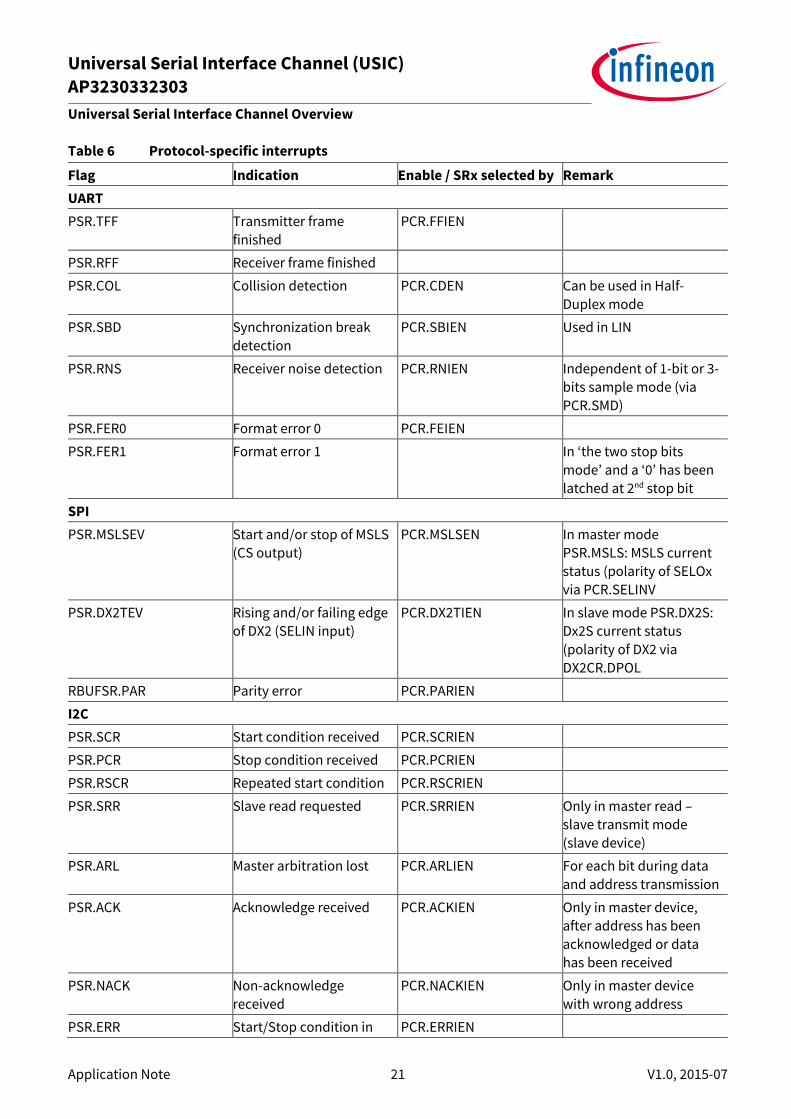
Table 6 Protocol-specific interrupts
Flag Indication Enable / SRx selected by Remark
UART
PSR.TFF Transmitter frame
finished
PCR.FFIEN
PSR.RFF Receiver frame finished
PSR.COL Collision detection PCR.CDEN Can be used in Half-
Duplex mode
PSR.SBD Synchronization break
detection
PCR.SBIEN Used in LIN
PSR.RNS Receiver noise detection PCR.RNIEN Independent of 1-bit or 3-
bits sample mode (via
PCR.SMD)
PSR.FER0 Format error 0 PCR.FEIEN
PSR.FER1 Format error 1 In ‘the two stop bits
mode’ and a ‘0’ has been
latched at 2nd stop bit
SPI
PSR.MSLSEV Start and/or stop of MSLS
(CS output)
PCR.MSLSEN In master mode
PSR.MSLS: MSLS current
status (polarity of SELOx
via PCR.SELINV
PSR.DX2TEV Rising and/or failing edge
of DX2 (SELIN input)
PCR.DX2TIEN In slave mode PSR.DX2S:
Dx2S current status
(polarity of DX2 via
DX2CR.DPOL
RBUFSR.PAR Parity error PCR.PARIEN
I2C
PSR.SCR Start condition received PCR.SCRIEN
PSR.PCR Stop condition received PCR.PCRIEN
PSR.RSCR Repeated start condition PCR.RSCRIEN
PSR.SRR Slave read requested PCR.SRRIEN Only in master read –
slave transmit mode
(slave device)
PSR.ARL Master arbitration lost PCR.ARLIEN For each bit during data
and address transmission
PSR.ACK Acknowledge received PCR.ACKIEN Only in master device,
after address has been
acknowledged or data
has been received
PSR.NACK Non-acknowledge
received
PCR.NACKIEN Only in master device
with wrong address
PSR.ERR Start/Stop condition in PCR.ERRIEN

Universal Serial Interface Channel (USIC)
AP3230332303
Universal Serial Interface Channel Overview
Application Note 22 V1.0, 2015-07
Flag Indication Enable / SRx selected by Remark
wrong position
PSR.TDF TDF error PCR.ERRIEN Wrong /undefined TDF
Figure 12 Channel Events and Interrupt Flags
Universal Serial Interface Channel (USIC)
AP3230332303
Universal Serial Interface Channel Overview
Application Note 23 V1.0, 2015-07
1.7 FIFO Data Buffer and Interrupts Events
The interrupts listed here are independent of the selected protocol. The following sequences should be
executed for initialization:
Bitfields xxINP of registers TBCTR and RBCTR define which SRx is activated if the corresponding event
occurs
Register TRBSR contains indication flags
Write a 1 to the corresponding bit position in register TRBSCR to clear its status bit in TRBSR
The interrupt priority level and enable/disable are controlled by Nested Vectored Interrupt Control
(NVIC) unit in XMC. See RM for more details about CMSIS functions to access ARM Cortex-M4 NVIC
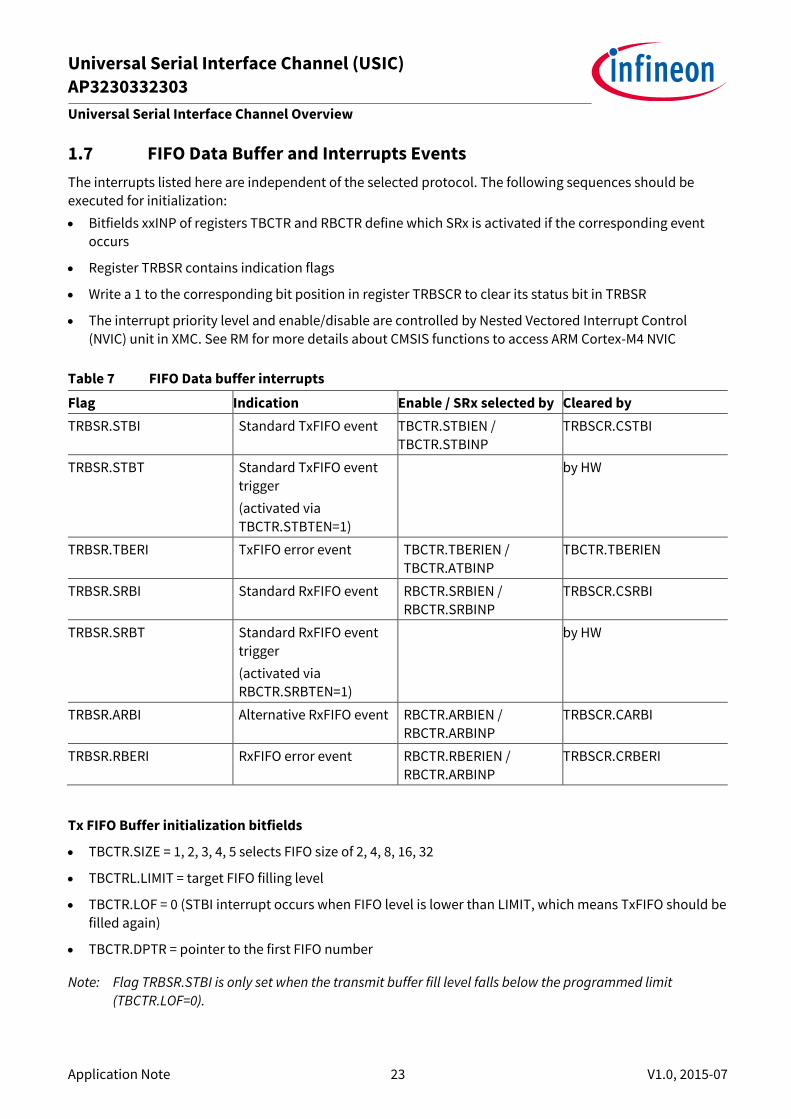
Table 7 FIFO Data buffer interrupts
Flag Indication Enable / SRx selected by Cleared by
TRBSR.STBI Standard TxFIFO event TBCTR.STBIEN /
TBCTR.STBINP
TRBSCR.CSTBI
TRBSR.STBT Standard TxFIFO event
trigger
(activated via
TBCTR.STBTEN=1)
by HW
TRBSR.TBERI TxFIFO error event TBCTR.TBERIEN /
TBCTR.ATBINP
TBCTR.TBERIEN
TRBSR.SRBI Standard RxFIFO event RBCTR.SRBIEN /
RBCTR.SRBINP
TRBSCR.CSRBI
TRBSR.SRBT Standard RxFIFO event
trigger
(activated via
RBCTR.SRBTEN=1)
by HW
TRBSR.ARBI Alternative RxFIFO event RBCTR.ARBIEN /
RBCTR.ARBINP
TRBSCR.CARBI
TRBSR.RBERI RxFIFO error event RBCTR.RBERIEN /
RBCTR.ARBINP
TRBSCR.CRBERI
Tx FIFO Buffer initialization bitfields
TBCTR.SIZE = 1, 2, 3, 4, 5 selects FIFO size of 2, 4, 8, 16, 32
TBCTRL.LIMIT = target FIFO filling level
TBCTR.LOF = 0 (STBI interrupt occurs when FIFO level is lower than LIMIT, which means TxFIFO should be
filled again)
TBCTR.DPTR = pointer to the first FIFO number
Note: Flag TRBSR.STBI is only set when the transmit buffer fill level falls below the programmed limit
(TBCTR.LOF=0).

Universal Serial Interface Channel (USIC)
AP3230332303
Universal Serial Interface Channel Overview
Application Note 24 V1.0, 2015-07
Rx FIFO Buffer initialization bitfield
RBCTR.SIZE= 1, 2, 3, 4, 5 selects FIFO size of 2, 4, 8, 16, 32.
RBCTRL.LIMIT = target FIFO filling level
RBCTR.LOF = 1 (SRBI interrupt occurs when FIFO level gets bigger than LIMIT, means RxFIFO should be
read out)
RBCTR.DPTR = pointer to the first FIFO number
RBCTR.RNM (optional)
Note: Flag TRBSR.SRBI is only set when the receive buffer fill level exceeds the programmed limit
(TBCTR.LOF=1).

Universal Serial Interface Channel (USIC)
AP3230332303
Synchronous Serial Channel (SSC = SPI)
Application Note 25 V1.0, 2015-07
2 Synchronous Serial Channel (SSC = SPI)
Figure 13 SPI Signal Connection in Full Duplex-Mode
This figure shows the standard SPI protocol, consisting of one input and one output data line. The XMC
family of products also supports two (dual-SPI) or four (quad-SPI) input/output data lines.
The SPI mode is selected when CCR.MODE = 0001B.
2.1 Input stages, Output Signals and the Protocol Pre-Process
Master mode
At DX1 the PPP uses the baud rate generator output SCLK directly as input for the data shift unit and gives
the signal SCLKOUT on the shift clock output pin.
At DX2 the PPP provides the output MSLS (Master SLave Signal) with the SPI specific delay, and uses it as
input for the data shift unit.
In SPI master mode, setting DX1 or DX2 is optionally used for delay compensation. The data input DX0/3/4/5
leads to the data shift unit and they are linked directly from the pins DINx. The PPP is not used and
DX0CR.INSW must be set to ‘1’.
Note: In a given application, the output pin SELO[7:0] is usually used as the Chip Select line (CS) for the SPI
device, and it normally has an active ’low’ level. In this case the polarity of the SELO signal has been
inverted by setting pin SELINV in the register PCR.

Universal Serial Interface Channel (USIC)
AP3230332303
Synchronous Serial Channel (SSC = SPI)
Application Note 26 V1.0, 2015-07
Slave mode
In SPI slave mode the PPP is not used in the input stages.
DX0/3/4/5, DX1, DX2 signals are linked directly from the pins DINx, SCLKIN and SELIN (set bit DXxCR.INSW to
‘1’).
Note: If a ’low’ active Chip Select line (CS) is used as input signal for the slave SPI device, its polarity must be
inverted (via DX2CR.DPOL).
In USIC SPI operation mode a re-synchronization is automatically performed by the CS signal.
In slave mode the DX2 signal is also used as a reset signal for its internal data shift unit. For example, after an
error during SPI communication it is possible to reset the state machine by generating an active DX2, single
input signal. Both master and slave use the USIC module, and the SPI master is switched off after 10 bits
rather than 16 bits have been transmitted, re-sending the Word again.
If the CS line is used (the 4-line SPI mode) then the slave device does not need special action to reset the
SPI channel. With the new CS edge sent by the master, the content of the internal shift register of the
slave is automatically reset and a new data word can be completely received by the slave. Only if the
FIFO is used do we need to flush the FIFO via register TRBSCR (bit FLUSHTB/ FLUSHRB)
Some applications use the 3-line SPI mode (CS is not used). If the USIC module is used as SPI slave then
we need to simulate a CS input signal (a falling edge for input DX2) to reset the internal data shift unit or
to reset the USIC module completely via PRSETx/PRCLRx
U1C0_DX2CR |= 0x0100; // set bit DPOL
U1C0_DX2CR &= (~(0x01000)); // clear bit DPOL
The data shift unit’s internal SCLK signal has an active ’high’ level so, if no SELIN (non-CS) is used, the
DX2 stage has to deliver a (permanent) 1-level to the data shift unit. This is achieved by programming
bitfield DX2CR.DSEL = 111B.
Note: In a multiplex CSx system, if a slave device is not selected (DX2 stage delivers a 0 to the data shift unit) a
shift clock pulse is received. In this case the shift clock pulses are ignored, the incoming data is not
received, and the DOUT0/3/4/5 outputs the passive level (SCTR.PDL)
2.2 Baud rate Generation
The baud rate of the SPI is defined by the frequency of the SCLK signal (one period of fSCLK represents one
data bit) and is only required in the master mode.
SPI baud rate generation is based on fPB (fsys) via BRG.CLKSEL=00B.
In a standard SPI application, the phase relation between MCLK and SCLK is not relevant, so the 2:1 divider
can be switched OFF (PPPEN=0).
Baud rate calculation (fractional divider mode):
If the phase relation is requested (using MCLK as the clock reference for external devices for example), then
the 2:1 divider must be switched ON (PPPEN=1).

Universal Serial Interface Channel (USIC)
AP3230332303
Synchronous Serial Channel (SSC = SPI)
Application Note 27 V1.0, 2015-07
2.3 Data Shifting and Handling
2.3.1 Data Transmission and Reception
Frame length (FLE):
The number of bits per frame
Word length (WLE):
For each data word control
USIC SPI Master Mode
In SPI master mode, the CSx (its internal signal is MSLS) is generated automatically by the PPP.
(PCR.MSLSEN must be set to ‘1’). This signal indicates the start and the end of a data transfer.
There are two ways to control the end of the frame:
Data frame length FLE < 63:
The frame is considered as finished and the remaining data bits in the last data word are not transferred
if the programmed number of bits per fame is reached within a data word
Data frame length FLE = 63:
The frame is considered as finished and the remaining data bits in the last data word are not transferred
if a de-activation of MSLS is detected within a data word
In master mode, frame transmission/reception can be started when the data in the transmit buffer TBUF is
valid (TCSR.TDV is set).
The internal signal MSLS is set together with the corresponding event flag (PSR.MSLS) and enters the first
leading delay state.
After the delay (Tld) generated by PPP has elapsed, the internal shift clock SCLK is issued, and the data is
shifted out at the rising edge of SCLK.
For every processed data bit when the falling edge of the shift clock SCLK is reached, the level of the input
signal is latched.
If FLE < 63 then a CS signal is generated automatically by the first data bit and deactivated at the end of
the last bit including delay Tld
If FLE = 63 then the user should give the start/end information of a data frame to create the desired
length of the CS signal. Bit TCSR.SOF/EOF is for this software-based control method
USIC SPI Slave Mode
In the case that the SELIN input signal (CSx) is used in slave mode, the data frame start/end detection is
based on the edge detection of input DX2 in both transmission and reception process. Data frame length
(SCTR.FLE) should be set to its maximum value (FLE=63).
In the case that the SELIN input signal is not used in slave mode, the data frame length must be
programmed to the known value (FLE<63).

Universal Serial Interface Channel (USIC)
AP3230332303
Synchronous Serial Channel (SSC = SPI)
Application Note 28 V1.0, 2015-07
Figure 14 Standard SPI Frame format with SCLKCFG=00B
2.3.2 SPI Frame Delay Control
SPI frame delay is generated automatically by the PPP in the SPI master mode based on fCTQIN.
Tld (leading delay):
Starts when data is valid for transmission. The first shift clock edge of SCLKis generated after the leading
delay. The data shift unit always uses the rising edge for data shifting and the latch edge for data
receiving
Ttd (trailing delay):
Starts at the end of the last SCLK cycle of a data frame. At the end point of the trailing delay the MSLS
becomes inactive. It corresponds to the slave hold-time requirements
Tnf (next-frame delay):
After the next-frame delay has elapsed, the frame is considered as finished
Tiw (inter-word delay):
Can be optionally enabled/disabled by PCR.TIWEN. It is used if a data frame consists of more than one
data word
In a standard SPI application, such as the setup and hold time, the Tld and Ttd are mainly used to ensure
stability on the input/output lines.
Normally fCTQIN = fSCLK via CTQSEL=10B.

Universal Serial Interface Channel (USIC)
AP3230332303
Synchronous Serial Channel (SSC = SPI)
Application Note 29 V1.0, 2015-07
Delay time calculation:
Note: Delay Tiw can be disabled via bit PCR.TIWEN
2.3.3 Shift Clock (SCLK) and CS
In master mode, the shift clock is generated by the internal baud rate generator.
In slave mode, the signal SCLKIN is received from an external master.
CS generation
If the SPI module is in master mode, the slave select signal (the internal signal MSLS) is generated
automatically by PPP.
SPI interfaces have 4 different configurations regarding the shift and latch edge for data transmission and
reception process.
Figure 15 Shift Clock in SPI Communication

Universal Serial Interface Channel (USIC)
AP3230332303
Synchronous Serial Channel (SSC = SPI)
Application Note 30 V1.0, 2015-07
USIC SPI master mode support
case 1 (SCLKCFG = 00B): No delay, no polarity inversion (SCLKOUT equals SCLK)
case 2 (SCLKCFG = 01B): No delay, polarity inversion
case 3 (SCLKCFG = 10B): SCLKOUT is delayed by 1/2 shift clock period, no polarity inversion
case 4 (SCLKCFG = 11B): is delayed by 1/2 shift clock period, polarity inversion
USIC SPI slave mode support (XMC4500)
case 1: no delay, no polarity inversion (SCLKOUT equals SCLK)
case 2: no delay, polarity inversion (SCLKOUT equals inverted SCLK): set DX1CR.DPOL to 1
Note: In slave mode bitfield SCLKCFG is ignored
In slave mode the shift clock signal is handled by the input stage DX1 (signal SCLKIN is received from an
external master), so the DX1 stage has to be connected to an input pin.
For case 1, the input signal on DX1 pin can be directly forwarded to the internal data shift unit.
For case 2, the DX1 stage must invert (set DX1CR.DPOL to 1) the received signal to adapt to the SCLKIN
polarity. This is because the internal data shift unit always takes data transmission on the rising edge and
data reception on the falling edge.
Note: In the XMC4400 and XMC1000 product families, the bit PCR.SLPHSEL is implemented to handle the shift
clock of the data shift unit to support case_3 and case_4 in SPI slave mode
2.3.4 Parity Mode
The XMC products support parity generation for transmission and parity check for reception on frame base
in master and slave mode. For consistency reasons, all communication partners must be programmed to
the same parity mode.
CCR.PM: define the type of parity. In SPI parity mode the clock extends by one cycle after the last data
word of the data frameindependent of SDIR setting (MSB or LSB).
RBUFSR.PAR: the monitored parity bit value.
PSR.PARERR: the result of the parity check
PCR.PARIEN: Parity Error Interrupt Enable
Note: For dual and quad SPI protocols, the parity bit is transmitted and received only on DOUT0 and DX0
respectively, in the extended clock cycle
Note: Parity bit generation or detection is not supported for a frame length > 64 data bits; i.e. setting FLE=0x3F
Universal Serial Interface Channel (USIC)
AP3230332303
Synchronous Serial Channel (SSC = SPI)
Application Note 31 V1.0, 2015-07
2.4 SPI Software configuration
2.4.1 SPI Full-Duplex Communication (Example 1)
A full-duplex system allows communication in both directions at the same time. Synchronous data transfer
is characterized by a simultaneous transfer of a shift clock signal together with transmit and receive data
signals.
Note: In the XM1000 family, only one USIC module is available. The FIFO and interrupt SRx are shared
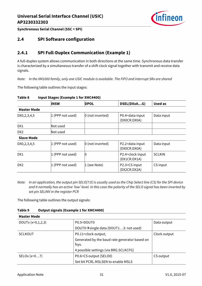
The following table outlines the input stages:
Table 8 Input Stages (Example 1 for XMC4400)
INSW DPOL DSEL(DXxA…G) Used as
Master Mode
DX0,2,3,4,5 1 (PPP not used) 0 (not inverted) P0.4=data input
(DX0CR.DX0A)
Data input
DX1 Not used
DX2 Not used
Slave Mode
DX0,2,3,4,5 1 (PPP not used) 0 (not inverted) P2.2=data input
(DX0CR.DX0A)
Data input
DX1 1 (PPP not used) 0 P2.4=clock input
(DX1CR.DX1A)
SCLKIN
DX2 1 (PPP not used) 1 (see Note) P2.3=CS input
(DX2CR.DX2A)
CS input
Note: In an application, the output pin SELO[7:0] is usually used as the Chip Select line (CS) for the SPI device
and it normally has an active ’low’ level. In this case the polarity of the SELO signal has been inverted by
set pin SELINV in the register PCR
The following table outlines the output signals:
Table 9 Output signals (Example 1 for XMC4400)
Master Mode
DOUTx (x=0,1,2,3) P0.5=DOUT0
DOUT0single data (DOUT1…3: not used)
Data output
SCLKOUT P0.11=clock output,
Generated by the baud rate generator based on
fsys.
4 possible settings (via BRG.SCLKCFG)
Clock output
SELOx (x=0…7) P0.6=CS output (SELO0)
Set bit PCRL.MSLSEN to enable MSLS
CS output

Universal Serial Interface Channel (USIC)
AP3230332303
Synchronous Serial Channel (SSC = SPI)
Application Note 32 V1.0, 2015-07
Master Mode
Set bit PCR.SELCTR to use CS direct select mode
Set bit field PCR.SELO to active the
corresponding SELOx output line
Set bit PCR.SELIN to invert MSLS for an active
‘low’ CS output signal
Slave mode
DOUTx (x=0,1,2,3) P2.5=DOUT0
DOUT0single data (DOUT1…3: not used)
Data output
SCLKOUT Not used
SELO[7:0] Not used
Note: 1. MSLS is an internal signal, which is active ‘high’. To generate the MSLS the bit PCR.MSLSEN must be
set.
2. Direct Select Mode: a SELOx output becomes active while the internal signal MSLS is active and bit x
in bit field SELO is 1. Several external slave devices can be addressed in parallel if more than one bit in
bit field SELO is set.
3. The output pin SELO [7:0] is usually used as the CS for SPI device and it normally has an active ’low’
level.
Data shift control (SCTR): TRM=01B, PDL=1, SDIR=1(MSB first), FLE=WLE=15
Data transmission control (TCSR): no trigger, no gating, single shot mode
Parity (CCR.PM): not used
Protocol-related information (PCR): SELO=1(P0.6=U1C0_CS0), FEM=1, SELINV=1, SELCTR=1, MSLSEN=1
Interrupts point (INPR) and enable control (CCR): INPR.AINP/RINP=SR2; CCR.AIEN/RIEN=1
Interrupt: enable AIR/RI interrupt via CMSIS functions: NVIC_SetPriority(..); NVIC_EnableIRQ(..)
Input/output pins configuration:
Output: PORTx->IOCRx.PC (alternate output function)
Table 10 Input/Output pins (Example 1 for XMC4400)
Input/output pins Function pin Port Driver (IOCRxPC)
Master mode
Data out U1C0_DOUT P0.5 ALT2 (push pull)
Clock output U1CO_SCLKOUT P0.11 ALT2 (push pull)
CS output U1CO_SEL0 P0.6 ALT2 (push pull)
Data input U1C0_DX0A P0.4 input
Slave mode
Data out U0C1_DX0A P2.2 input
Clock input U0C1_DX1A P2.4 input
CS input U0C1_DX2A P2.3 input
Data output U0C1_DOUT P2.5 ALT2 (push pull)

Universal Serial Interface Channel (USIC)
AP3230332303
Synchronous Serial Channel (SSC = SPI)
Application Note 33 V1.0, 2015-07
2.4.2 Software in Loopback mode (Example 2)
Note: This is only applicable in master mode
We use the same initialization routine as that in Example 1, until DX0CR.DSEL which must be set to “G”
(110B).
Note: In loop-back mode the data output pins are not required to be switched on, but if they are then the
signal can be monitored on an oscilloscope.
2.4.3 SPI for Half- Duplex Communication
In half-duplex mode only one data line is shared between the communication partners and it is used for
both transmission and reception of data (MRST and MTSR are connected together).
The user software must ensure that only one transmitter is active at a time.
There are two ways to avoid collisions on the data exchange line:
Only the transmitting channel may enable its transmit pin driver (enable/disable push/pull drivers)
Devices use open-drain outputs to allow the wired-AND connection in a multi-transmitter
communication
The SPI data transfer is synchronized by a simultaneous transfer of a shift clock signal together with the
transmission and reception of the data signal. Therefore, the dummy data of the register TBUF in an inactive
partner should be set to all 1’s.
2.4.3.1 Standard SPI Half-Duplex System (Example 3)
In the following figure, the master mode uses an internal connection with the output pin DOUT. The slave
mode uses an external connection between DOUT and DIN pins. Internal connection means DX0x points to
DOUT. For example, XMC1100, P1.0 => U0C0_DX0C => U0C0_DOUT.

Universal Serial Interface Channel (USIC)
AP3230332303
Synchronous Serial Channel (SSC = SPI)
Application Note 34 V1.0, 2015-07
Figure 16 Signal Connection for SPI Standard Half-Duplex System
Note: Not all the data output DOUTx pins contain an internal connection. For example, P1.5 (as U0C0_DOUT0)
has an internal connection to DX0 (U0C0_DX0A), but P1.7 (U0C0_DOUT) has no such connection in
XMC4000 family
Initialization routine
This example uses the same initialization routine as for Example 1, but with the changes indicated in the
following table:
Table 11 Standard SPI Half-Duplex system initialization (Example 3 for XMC4000)
Input/output pins Function pin Port Driver (IOCRxPC)
Master mode Internal connection is used
Data out U1C0_DOUT P0.5 ALT2 (push pull)
Clock output U1CO_SCLKOUT P0.11 ALT2 (push pull)
CS output U1CO_SEL0 P0.6 ALT2 (push pull)
Data input U1C0_DX0A U1C0_DX0B (see
note)
P0.4 P0.5 (see
note)
input
Slave mode External connection is used
Data out U0C1_DX0A P2.2 input
Clock input U0C1_DX1A P2.4 input
CS input U0C1_DX2A P2.3 input
Data output U0C1_DOUT P2.5 ALT2 (push pull)
Note: Instead of P0.4, we use P0.5 as data input U1C0_DX0 (the internal connection mode is used)

Universal Serial Interface Channel (USIC)
AP3230332303
Synchronous Serial Channel (SSC = SPI)
Application Note 35 V1.0, 2015-07
2.4.3.2 Hardware-controlled SPI Half-Duplex Sytem
Hardware-port pin control is implemented for the XMC family of products. One, two or four port pins can be
selected with the hardware port control to support SPI protocols with multiple bi-directional data lines,
such as dual and quad- SPI. This selection, and the enable/disable of the hardware port control, is made
through CCR.HPCEN.
USIC is usually used as master mode. For data transmission direction hardware pins must be switched as
input or output. The direction of all selected pins is controlled through a single bit, SCTR.HPCDIR.
SCTR.HPCDIR is automatically shadowed with the start of each data word to prevent the pin changing
direction in the middle of a data word transfer.
In the XMC family, several peripherals have hardware controlled pins. Because multiple peripheral I/Os are
mapped on some pins, the register Pn_HWSEL is used to select which peripheral has control over the pin.
In XMC4000 products, all USIC hardware-controlled pins use the HW0 control path (Pn_HWSEL.HWx=01B).
In XMC1000 products, all USIC hardware-controlled pins use the HW1 control path (Pn_HWSEL.HWx=10B).
Note: In the XMC4500 144 pin package, each channel (2 channels per module) has hardware-control pins, but
in XMC1100 only U0C0 can use this feature and U0C1 does not have any hardware-control pins.
2.5 Delay Compensation
For the SPI protocol, USIC works with fsys/2 (40Mbaud/fsys=80MHz). This maximum baud rate is based on
module capability. In the application environment it is limited by several factors, including driver delays,
signal propagation times, synchronization and filter delay, and so on. In the data receive process, the
minimum required setup time must also be considered.

Universal Serial Interface Channel (USIC)
AP3230332303
Synchronous Serial Channel (SSC = SPI)
Application Note 36 V1.0, 2015-07
Figure 17 SPI Master Mode with Delay Compensation
Figure 18 SPI Complete Closed-loop Delay Compensation

Universal Serial Interface Channel (USIC)
AP3230332303
Synchronous Serial Channel (SSC = SPI)
Application Note 37 V1.0, 2015-07
The closed-loop delay is a system-inherent factor. The delay time between the generation of the shift clock
signal and the evaluation of the receive data by the master SPI module is given by the sum = Tout_master + 2 x
Tprop + Tin_slave + Tout_slave + Tin_master + module reaction times, where:
Tout_master/Tout_slave
− Delay time through the output driver stage to the pin (default setting A1+/A2 pin: falling/rising
time<16ns. Please refer to the appropriate data sheet)
Tprop
− Delay time on the wires
Tin_slave/Tin_master:
− Delay time through the input pin to the module input stage
Module reaction times
− Delay time due to digital filter, synchronization, setup/hold time (Please refer to the appropriate data
sheet)

Universal Serial Interface Channel (USIC)
AP3230332303
Synchronous Serial Channel (SSC = SPI)
Application Note 38 V1.0, 2015-07
Figure 19 SPI Signals delay Timing Waveform
Using the default standard setting, as data is received in the master SPI process, the clock signal (signal 1 in
this example figure) generated from the baud rate generator in the master device, is used to latch a data
signal (signal 5). For a higher baud rate, this may lead to incorrect data being latched. A higher baud rate can
be reached by using a delay compensation feature.
In XMC there are two compensation methods: delay compensation and complete closed-loop delay
compensation.

Universal Serial Interface Channel (USIC)
AP3230332303
Synchronous Serial Channel (SSC = SPI)
Application Note 39 V1.0, 2015-07
Delay compensation in master mode
This method uses the input clock signal at the DX1 pin for data latching, instead of the SCLKOUT generated
by the baud rate generator (signal 6 and 5 in Figure 19).
With this method, the clock output driver delay in master mode is compensated. This means the delay
between the evaluated clock signal and Rx data by master is reduced by Tin_master + Tout_master.
Example 4 demonstrates the initialization routine using delay compensation in master mode.
An external or an internal connection can be used:
External connection
− P0.8 U0C0_SCLKOUT, P1.1 U0C0_DX1A
USIC0_CHo DX1CR |= (0<<0); // DX1CR.DSEL=A
USIC0_CHo DX1CR |= (1<<4); // DX1CR. INSW=1
− P1.1 (U0C0_DX1A) has to be connected with P0.8 (U0C0_SCLKOUT) externally
Internal connection
− P0.8 U1C0_SCLKOUT, P0.8 U1C0_DX1B
USIC0_CHo DX1CR |= (1<<0); // DX1CR.DSEL=B
USIC0_CHo DX1CR |= (1<<4); // DX1CR. INSW=1
Note: 1. The internal connection can only be used for a bi-directional clock pin and it does not lead to
additional pins for the SPI communication.
2. Bit DCEN is implemented in XMC to allow the Rx shift clock to be controlled independently from the Rx
shift clock. When DCEN=1, the Tx shift clock is taken from the baud rate generator directly.
Complete closed-loop compensation
Note: This is implemented in the XMC4400 and XMC1000 product families, but not in the XMC4500 family.
The principle behind this method is to feedback the clock signal to the master mode, so that the master can
use this clock signal to latch data from the slave. Because the clock signal is through the complete closed-
loop signal path, the delay between the clock used in the master and data (from the slave) signal is therefore
fully compensated.
This method can only be realized when both master and slave use the USIC module. In slave mode the
CLKOUT pin should be enabled by setting BRG.SCLKOSEL to 1.

Universal Serial Interface Channel (USIC)
AP3230332303
Synchronous Serial Channel (SSC = SPI)
Application Note 40 V1.0, 2015-07
Table 12 Example 4 for XMC4000
U0C0 in master
Data out DOUT0 P1.5 ALT2 (A1+)
Clock output SCLKOUT P0.8 ALT2 (A2)
CS output SELO0 P0.7 ALT2 (A2)
Data input DIN (DX0) P1.4 DX0B, input (A1+)
Clock input SCLKIN (DX1) P1.1 DX1A, input (A1+) external connection for
delay compensation in
master mode
U0C0 in slave
Data input DIN (DX0) P2.2 DX0A, input (A2)
Clock input SCLKIN (DX1) P2.4 DX1A, input (A2)
CS input CS input (DX2) P2.3 DX2A, input (A2)
Data ouput DOUT0 P2.5 ALT2 (A2)
2.6 Multiple MSLS Output Signals
The SPI module supports up to 8 different SELOx output signals for master mode operation in one USIC
module. USIC provides two configuration modes to select the MSLS signal:
Direct control mode
− Write PCR.SELO[7:0] as individual values for each SELOx line
Automatic update mode
− Enabled by TCSR.SELMD=1
− PCR.SELO[4:0] is updated with TCI[4:0] and PCR.SELO[7:5] is always ’0’
Each USIC module has the transmit buffer input locations TBUFx (x=00-31), addressed by using 32
consecutive addresses.
If TCSR.SELMD = 1, data written to one of these locations appears in a common TBUF register, and the 5-bit
TCI [4:0] coding is updated accordingly.
The relationship between TBUFx, TCI[x] and MSELx is listed in following table.
Table 13
Write to TBUFx TCI [4:0] PCRH:SELO [7:0] SELOx signals
TBUF01 00001B 0000,0001B SELO0 active
TBUF02 00010B 0000,0010B SELO1 active
TBUF04 00100B 0000,0001B SELO2 active
TBUF08 01000B 0000,0100B SELO3 active
TBUF16 10000B 0001,0000B SELO4 active
TBUF03 00011B 0000,0011B SELO0/1 active
TBUF07 00111B 0000,0111B SELO0 /1/2 active
TBUF00 00000B 0000,0001B No SELOx

Universal Serial Interface Channel (USIC)
AP3230332303
Synchronous Serial Channel (SSC = SPI)
Application Note 41 V1.0, 2015-07
2.7 XMC Lib Implementation: Full-Duplex mode
This example is for the XMC4400 and demonstrates how to use the USIC for an SPI communication in full-
duplex mode.
Channel 1 of the USIC slice 0, channel 0 of the USIC slice 1 and the PORTs 0.4, 0.5, 0.6, 0.11, 2.2, 2.3, 2.4, 2.5
are used.
2.7.1 Configuration
The SPI bus specifies four logic signals:
SCLK Serial Clock (output from master)
MOSI Master Output-Slave Input (output from master)
MISO Master Input-Slave Output (output from slave)
SS stands for Slave Select (active low, output from master)
In this example, 2 channels of USIC are used: USIC1CH0 and USIC0CH1.
The configuration of the SPI protocol needs the baudrate for both for Master and Slave to be set with the
same value. In addition, the bus modes are configured: SPI Master for the Master and SPI Slave for the Slave.
Master needs a configuration for the polarity of the Slave, which can be the same for both (active high) or
inverted (active low).
At the end it is possibile to choose the eventual bit for the parity mode.
XMC_USIC_CH_t *spi_master_ch = XMC_SPI1_CH0;
XMC_USIC_CH_t *spi_slave_ch = XMC_SPI0_CH1;
XMC_SPI_CH_CONFIG_t spi_config_masterMode;
XMC_SPI_CH_CONFIG_t spi_config_slaveMode;
spi_config_masterMode.baudrate = 100000;
spi_config_masterMode.bus_mode = XMC_SPI_CH_BUS_MODE_MASTER;
spi_config_masterMode.selo_inversion = XMC_SPI_CH_SLAVE_SEL_SAME_AS_MSLS;
spi_config_masterMode.parity_mode = XMC_USIC_CH_PARITY_MODE_NONE;
spi_config_slaveMode.bus_mode = XMC_SPI_CH_BUS_MODE_SLAVE;
spi_config_slaveMode.parity_mode = XMC_USIC_CH_PARITY_MODE_NONE;

Universal Serial Interface Channel (USIC)
AP3230332303
Synchronous Serial Channel (SSC = SPI)
Application Note 42 V1.0, 2015-07
Table 14 Input/Output pins SPI FULL-Duplex mode
Input/output pins Function pin Port Driver (IOCRxPC)
Master mode
Data out U1C0_DOUT P0.5 ALT2 (push pull)
Clock output U1CO_SCLKOUT P0.11 ALT2 (push pull)
CS output U1CO_SEL0 P0.6 ALT2 (push pull)
Data input U1C0_DX0A P0.4 input
Slave mode
Data out U0C1_DX0A P2.2 input
Clock input U0C1_DX1A P2.4 input
CS input U0C1_DX2A P2.3 input
Data output U0C1_DOUT P2.5 ALT2 (push pull)
2.7.2 Initialization
The initialization of the USIC channel for an SPI communication requires a specific sequence of commands.
First, the init function is called in order to initialize the selected SPI channel with the config structure.
After this, the USIC channel is started in SPI mode.
Finally, the data source for the SPI input stage is selected.
For the master:
XMC_SPI_CH_Init(spi_master_ch, &spi_config_masterMode);
XMC_SPI_CH_Start(spi_master_ch);
XMC_SPI_CH_SetInputSource(spi_master_ch,XMC_SPI_CH_INPUT_DIN0,
USIC1_C0_DX0_P0_4);
For the slave:
XMC_SPI_CH_Init(spi_slave_ch, &spi_config_slaveMode);
XMC_SPI_CH_Start(spi_slave_ch);
XMC_SPI_CH_SetInputSource(spi_slave_ch, XMC_SPI_CH_INPUT_DIN0,
USIC0_C1_DX0_P2_2);
XMC_SPI_CH_SetInputSource(spi_slave_ch, XMC_SPI_CH_INPUT_SLAVE_SCLKIN,
USIC0_C1_DX1_P2_4);
XMC_SPI_CH_SetInputSource(spi_slave_ch, XMC_SPI_CH_INPUT_SLAVE_SELIN,
USIC0_C1_DX2_P2_3);
For the communication, it is useful to set the length of the data.
XMC_SPI_CH_SetWordLength(spi_master_ch, 16);
XMC_SPI_CH_SetWordLength(spi_slave_ch, 16);
Universal Serial Interface Channel (USIC)
AP3230332303
Synchronous Serial Channel (SSC = SPI)
Application Note 43 V1.0, 2015-07
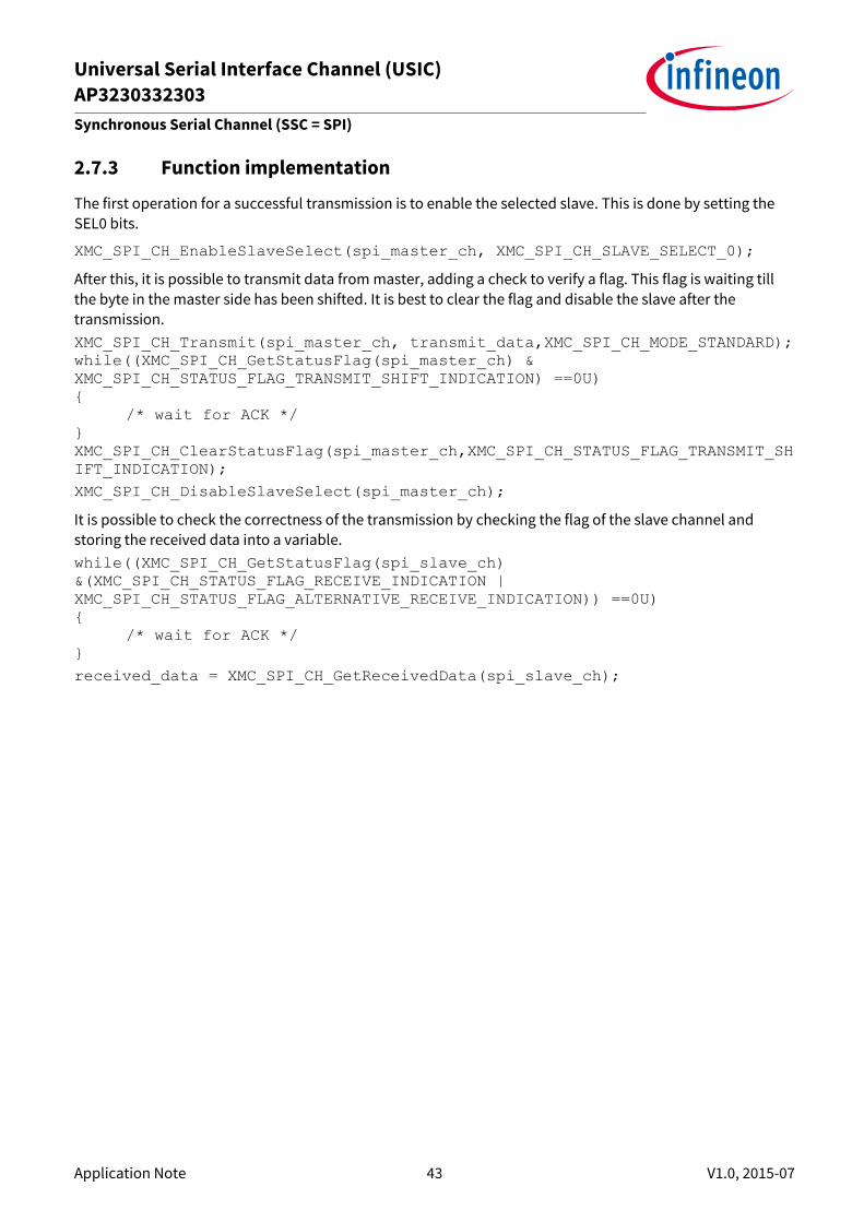
2.7.3 Function implementation
The first operation for a successful transmission is to enable the selected slave. This is done by setting the
SEL0 bits.
XMC_SPI_CH_EnableSlaveSelect(spi_master_ch, XMC_SPI_CH_SLAVE_SELECT_0);
After this, it is possible to transmit data from master, adding a check to verify a flag. This flag is waiting till
the byte in the master side has been shifted. It is best to clear the flag and disable the slave after the
transmission.
XMC_SPI_CH_Transmit(spi_master_ch, transmit_data,XMC_SPI_CH_MODE_STANDARD);
while((XMC_SPI_CH_GetStatusFlag(spi_master_ch) &
XMC_SPI_CH_STATUS_FLAG_TRANSMIT_SHIFT_INDICATION) ==0U)
{
/* wait for ACK */
}
XMC_SPI_CH_ClearStatusFlag(spi_master_ch,XMC_SPI_CH_STATUS_FLAG_TRANSMIT_SH
IFT_INDICATION);
XMC_SPI_CH_DisableSlaveSelect(spi_master_ch);
It is possible to check the correctness of the transmission by checking the flag of the slave channel and
storing the received data into a variable.
while((XMC_SPI_CH_GetStatusFlag(spi_slave_ch)
&(XMC_SPI_CH_STATUS_FLAG_RECEIVE_INDICATION |
XMC_SPI_CH_STATUS_FLAG_ALTERNATIVE_RECEIVE_INDICATION)) ==0U)
{
/* wait for ACK */
}
received_data = XMC_SPI_CH_GetReceivedData(spi_slave_ch);

Universal Serial Interface Channel (USIC)
AP3230332303
Asynchronous Serial Channel (ASC = UART)
Application Note 44 V1.0, 2015-07
3 Asynchronous Serial Channel (ASC = UART)
Figure 20 UART Signals Connection for Full-Duplex Communication
An UART connection is characterized by the use of a single connection line between a transmitter and a
receiver. The receiver input RXD signal is handled by the input stage DX0. For full-duplex communication, an
independent communication line is needed for each transfer direction. Figure 20 shows an example with a
point-to-point full-duplex connection between two communication partners UART A and UART B.
For half-duplex or multi-transmitter communication, a single communication line is shared between the
communication partners. Figure 21 shows an example with a point-to-point half-duplex connection
between UART A and UART B. In this case, the user has to take care that only one transmitter is active at a
time. In order to support transmitter collision detection, the input stage DX1 can be used to monitor the
level of the transmit line and to check if the line is in the idle state or if a collision occurred.
There are two possibilities to connect the receiver input DIN0 to the transmitter output DOUT0.
Communication partner UART A uses an internal connection with only the transmit pin TXD that delivers its
input value as RXD to the DX0 input stage for reception and to DX1 to check for transmitter collisions.
Communication partner UART B uses an external connection between the two pins TXD and RXD.

Universal Serial Interface Channel (USIC)
AP3230332303
Asynchronous Serial Channel (ASC = UART)
Application Note 45 V1.0, 2015-07
Figure 21 UART Signals Connection for Half-Duplex Communication
3.1 Frame Format
A standard UART frame consists of:
An idle time with the signal level 1
One start of frame bit (SOF) with the signal level 0
A data field containing a programmable number of data bits (1-63)
A parity bit (P), programmable for either even or odd parity. It is optionally possible to handle frames
without a parity bit
One or two stop bits with the signal level 1
Figure 22 Standard UART Frame Format
The protocol specific bits (SOF, P, STOP) are automatically handled by the UART protocol state machine and
do not appear in the data flow via the receive and transmit buffers.

Universal Serial Interface Channel (USIC)
AP3230332303
Asynchronous Serial Channel (ASC = UART)
Application Note 46 V1.0, 2015-07
3.2 Baud Rate Generation
The baud rate fASC in UART mode depends on the number of time quanta per bit time and their timing. The
baud rate setting should only be changed while the transmitter and the receiver are idle. The bits in register
BRG define the baud rate setting:
BRG.CTQSEL:
defines the input frequency fCTQIN for the time quanta generation
BRG.PCTQ:
defines the length of a time quantum (division of fCTQIN by 1, 2, 3, or 4)
BRG.DCTQ:
defines the number of time quanta per bit time
The standard setting is given by CTQSEL = 00B (fCTQIN = fPDIV) and PPPEN = 0 (fPPP = fPIN). Under these
conditions, the baud rate is given by:
In order to generate slower frequencies, two additional divide-by-2 stages can be selected by CTQSEL = 10B
(fCTQIN = fSCLK) and PPPEN = 1 (fPPP = fMCLK), leading to:
3.3 XMC Lib Implementation: Full-Duplex mode
This example demonstrates how to use the USIC for an UART communication in a full-duplex mode.
The communication is established between the XMC4500 and a PC and it sends a “ Hello World” message.
The example is made for the XMC4500, the USIC channel, PORT 1.4 and PORT 1.5.
It also requires a terminal tool, like MTTTY, PuTTY or HTerm.
3.3.1 Configuration
UART channel configuration:
The UART protocol needs only two data lines (Tx and Rx). For a proper configuration, the parameters to set
are baudrate, oversampling, frame length, number of data bits, stop bits and parity mode bit.
Universal Serial Interface Channel (USIC)
AP3230332303
Asynchronous Serial Channel (ASC = UART)
Application Note 47 V1.0, 2015-07
In this example:
The baudrate for the USIC peripheral is selected equal to 57600 baud and the chosen channel is
XMC_UART0_CH0.
The number of bits is the number of bits for the data field. The minimum value allowed is 1, the
maximum is 16. For this example, the value is 8.
The frame length indicates the number of bits in a frame. The minimum value allowed is 1, the maximum
is 63. For this example, the value is 8.
The oversampling refers to the number of samples for a symbol (DCTQ Denominator Counter for Time
Quanta). The minimum value allowed is 1, the maximum is 32. For this example, the value is 16.
In addition, Stop bits are set to the default and standard value of 1.
Finally, the parity mode is set to none because it is not used.
XMC_USIC_CH_t *uart = XMC_UART0_CH0;
XMC_UART_CH_CONFIG_t uart_config = {
.baudrate = 57600U,
.oversampling = 16U,
.data_bits = 8U,
.frame_length = 8U,
.stop_bits = 1U,
.parity_mode = XMC_USIC_CH_PARITY_MODE_NONE
} ;
Table 15 Input/Output pins for UART Full-Duplex mode
Input/Output pins Function pin Port Driver (IOCRxPC)
Data out USIC0_CH0.DOUT0 P1.5 ALT 2 (push pull)
Data in USIC0_CH0.DX0B P1.4 input
3.3.2 Initialization
The initialization sequence is important. Make sure that the input source is selected before starting the USIC
peripheral. In order to avoid spikes, the GPIO ports should be initialized after the start of the USIC channel.
XMC_UART_CH_Init(uart, &uart_config);
XMC_UART_CH_SetInputSource(uart, XMC_UART_CH_INPUT_RXD ,USIC0_C0_DX0_P1_4);
XMC_UART_CH_Start(uart);
3.3.3 Function implementation
The USIC peripheral set with UART protocol is ready to transmit. For simpler code, it is best to store the
message in a variable and use a for-loop.
uint8_t message[] = "Hello World!\n";
for (uint8_t index = 0; index < sizeof(message) - 1; index++)

Universal Serial Interface Channel (USIC)
AP3230332303
Asynchronous Serial Channel (ASC = UART)
Application Note 48 V1.0, 2015-07
{
XMC_UART_CH_Transmit(XMC_UART0_CH0, message[index]);
}
The final stage is to see the output of the transmission in a terminal tool. The terminal tool needs to use the
virtual COM port that is connected to the MCU and the baudrate must be set according to the value in the
code (57600).
3.4 XMC Lib Implementation: Loopback mode
This example demonstrated the loopback feature of the UART. This function permits to evaluate the USIC
channel directly on-chip without any connections to port pins.
The example is made for the XMC4500. The USIC channel and the input is DX0G which is used only for the
loopback feature.
3.4.1 Configuration
UART Channel configuration:
The UART configuration is the same as the previous example.
XMC_USIC_CH_t *uart = XMC_UART0_CH0;
XMC_UART_CH_CONFIG_t uart_config = {
.baudrate = 57600U,
.oversampling = 16U,
.data_bits = 8U,
.frame_length = 8U,
.stop_bits = 1U,
.parity_mode = XMC_USIC_CH_PARITY_MODE_NONE
} ;
3.4.2 Initialization
In this example, the configuration of Tx pin for an alternate function is not required. The initialization
sequence is the same as in the previous example, but the Input Source is different.
XMC_UART_CH_Init(uart, &uart_config);
XMC_UART_CH_SetInputSource(uart, XMC_USIC_CH_INPUT_DX0,USIC0_C0_DX0_DOUT0);
XMC_UART_CH_Start(uart);
3.4.3 Function implementation
In this example, the code polls for the end of the transmission by checking the flags provided by UART. When
one of these flags is 0, it means the transmission is correct. The last step is to get the result of the
transmission from the UART.
uint16_t TxData, RxData;
TxData=0xAA;
XMC_UART_CH_Transmit(uart, TxData);
Universal Serial Interface Channel (USIC)
AP3230332303
Asynchronous Serial Channel (ASC = UART)
Application Note 49 V1.0, 2015-07
while((XMC_UART_CH_GetStatusFlag(uart)
&(XMC_UART_CH_STATUS_FLAG_RECEIVE_INDICATION |
XMC_UART_CH_STATUS_FLAG_ALTERNATIVE_RECEIVE_INDICATION)) == 0){}
RxData= XMC_UART_CH_GetReceivedData(uart);
3.5 XMC Lib Implementation: Half-Duplex mode
The UART protocol permits communication with only a single data signal line for transmit and receive.
This method is useful because the potential for collisions is totally avoided. Only one UART device at a time
enables its transmit pin (with push-pull configuration).
In the USIC peripheral, it is possible to have an external as well as internal connection.
3.5.1 Configuration
UART Channel configuration:
The UART configuration is the same as the previous example.
XMC_USIC_CH_t *uart = XMC_UART0_CH0;
XMC_UART_CH_CONFIG_t uart_config = {
.baudrate = 57600U,
.oversampling = 16U,
.data_bits = 8U,
.frame_length = 8U,
.stop_bits = 1U,
.parity_mode = XMC_USIC_CH_PARITY_MODE_NONE
} ;
3.5.2 Initialization
In this example, the configuration is using the internal connection of the pin so that the pin is used as DOUT
and DIN.
Table 16 Input/Output pins for UART Half-Duplex mode
Input/Output pins Function pin Port Driver (IOCRxPC)
Data out USIC0_CH0.DOUT0 P1.5 ALT 2 (push pull)
Data in USIC0_CH0.DX0A P1.5 input
XMC_UART_CH_Init(uart, &uart_config);
XMC_UART_CH_SetInputSource(uart, XMC_USIC_CH_INPUT_DX0,USIC0_C0_DX0_P1_5);
XMC_UART_CH_Start(uart);
3.5.3 Function implementation
The function implementation for this example is the same as the previous example.

Universal Serial Interface Channel (USIC)
AP3230332303
Asynchronous Serial Channel (ASC = UART)
Application Note 50 V1.0, 2015-07
uint16_t TxData, RxData;
TxData=0xAA;
XMC_UART_CH_Transmit(uart, TxData);
while((XMC_UART_CH_GetStatusFlag(uart)
&(XMC_UART_CH_STATUS_FLAG_RECEIVE_INDICATION |
XMC_UART_CH_STATUS_FLAG_ALTERNATIVE_RECEIVE_INDICATION)) == 0){}
RxData= XMC_UART_CH_GetReceivedData(uart);
3.6 XMC Lib Implementation: Loopback mode with FIFO
This example shows the possibility to use the optional functionality of the FIFO RAM. For correct usage, FIFO
RAM must be initialized separately before being used.
3.6.1 Configuration
UART Channel configuration:
The UART configuration is the same as the previous example.
XMC_USIC_CH_t *uart = XMC_UART0_CH0;
XMC_UART_CH_CONFIG_t uart_config = {
.baudrate = 57600U,
.oversampling = 16U,
.data_bits = 8U,
.frame_length = 8U,
.stop_bits = 1U,
.parity_mode = XMC_USIC_CH_PARITY_MODE_NONE
} ;
The configuration of the FIFO requires a parameter of the FIFO size expressed in number of Words.
Additionally, the value of the limit and the first FIFO number (start point) are required.
In this example the FIFO of the TX channel is configured with 8 entries for TxFIFO from point 0, with a limit of
1. The RX channel is configured with 8 entries for RxFIFO from point 16, with a limit of 7. This means that
SRBI is set if all 8*DATA items have been received. This SRBI (Standard Receive Buffer) bit indicates that a
standard receive buffer eventhas been detected.
XMC_USIC_CH_TXFIFO_Configure(uart, 0, XMC_USIC_CH_FIFO_SIZE_8WORDS, 1);
XMC_USIC_CH_RXFIFO_Configure(uart, 16, XMC_USIC_CH_FIFO_SIZE_8WORDS, 7);
3.6.2 Function implementation
This example uses two APIs dedicated for the FIFO. One is dedicated to insert data FIFO during the
Transmission phase, the other is used to get data in the Reception phase.
uint16_t uwaTxData[8], uwaRxData[8], i;
for (i=0; i<8; i++)

Universal Serial Interface Channel (USIC)
AP3230332303
Asynchronous Serial Channel (ASC = UART)
Application Note 51 V1.0, 2015-07
{
uwaTxData[i] = (0x55 + i);
XMC_USIC_CH_TXFIFO_PutData(uart, uwaTxData[i]);
}
while((XMC_USIC_CH_RXFIFO_GetEvent(uart) & USIC_CH_TRBSR_SRBI_Msk) == 0){}
for (i=0; i<8; i++)
{
uwaRxData[i] = XMC_USIC_CH_RXFIFO_GetData(uart);
if (uwaTxData[i] != uwaRxData[i]) while (1);
}
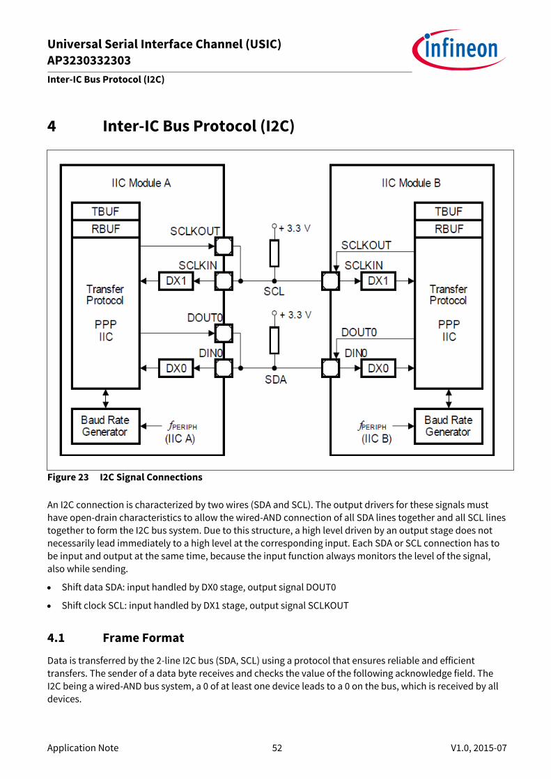
Universal Serial Interface Channel (USIC)
AP3230332303
Inter-IC Bus Protocol (I2C)
Application Note 52 V1.0, 2015-07
4 Inter-IC Bus Protocol (I2C)
Figure 23 I2C Signal Connections
An I2C connection is characterized by two wires (SDA and SCL). The output drivers for these signals must
have open-drain characteristics to allow the wired-AND connection of all SDA lines together and all SCL lines
together to form the I2C bus system. Due to this structure, a high level driven by an output stage does not
necessarily lead immediately to a high level at the corresponding input. Each SDA or SCL connection has to
be input and output at the same time, because the input function always monitors the level of the signal,
also while sending.
Shift data SDA: input handled by DX0 stage, output signal DOUT0
Shift clock SCL: input handled by DX1 stage, output signal SCLKOUT
4.1 Frame Format
Data is transferred by the 2-line I2C bus (SDA, SCL) using a protocol that ensures reliable and efficient
transfers. The sender of a data byte receives and checks the value of the following acknowledge field. The
I2C being a wired-AND bus system, a 0 of at least one device leads to a 0 on the bus, which is received by all
devices.

Universal Serial Interface Channel (USIC)
AP3230332303
Inter-IC Bus Protocol (I2C)
Application Note 53 V1.0, 2015-07
A data word consists of 8 data bit symbols for the data value, followed by another data bit symbol for the
acknowledge bit. The data word can be interpreted as address information (after a start symbol) or as
transferred data (after the address).
In order to be able to receive an acknowledge signal, the sender of the data bits has to release the SDA line
by sending a 1 as the acknowledge value. Depending on the internal state of the receiver, the acknowledge
bit is either sent active or passive.
Figure 24 I2C Frame Example
4.2 Symbol Timing
The symbol timing of the I2C is determined by the master stimulating the shift clock line SCL.
100 kBaud standard mode (PCR.STIM = 0):
− The symbol timing is based on 10 time quanta tq per symbol. A minimum module clock frequency
fPERIPH = 2 MHz is required
400 kBaud fast mode (PCR.STIM = 1):
− The symbol timing is based on 25 time quanta tq per symbol. A minimum module clock frequency
fPERIPH = 10 MHz is required
The baud rate setting should only be changed while the transmitter and the receiver are idle or CCR.MODE =
0.
The bits in register BRG define the length of a time quantum tq that is given by one period of fPCTQ.
BRG.CTQSEL:
defines the input frequency fCTQIN for the time quanta generation
BRG.PCTQ:
defines the length of a time quantum (division of fCTQIN by 1, 2, 3, or 4)

Universal Serial Interface Channel (USIC)
AP3230332303
Inter-IC Bus Protocol (I2C)
Application Note 54 V1.0, 2015-07
BRG.DCTQ:
defines the number of time quanta per symbol (number of tq = DCTQ + 1)
The standard setting is given by CTQSEL = 00B (fCTQIN = fPDIV) and PPPEN = 0 (fPPP = fIN). Under these
conditions, the frequency fPCTQ is given by:
4.3 Data Flow Handling
The handling of the data flow and the sequence of the symbols in an I2C frame is controlled by the I2C
transmitter part of the USIC communication channel.
The I2C bus protocol is byte-oriented, whereas a USIC data buffer word can contain up to 16 data bits. In
addition to the data byte to be transmitted (located at TBUF[7:0]), bit field TDF (transmit data format) to
control the I2C sequence is located at the bit positions TBUF[10:8].
Alternatively, polling of the ACK and NACK bits in PSR register can be performed, and the next data byte is
transmitted only after an ACK is received.
Table 17 Master Transmit Data Formats
TDF Code Description
000B Send data byte as master
This format is used to transmit a data byte from the master to a slave. The transmitter sends
its data byte (TBUF[7:0]), receives and checks the acknowledge bit sent by the slave.
010B Receive data byte and send acknowledge
This format is used by the master to read a data byte from a slave. The master acknowledges
the transfer with a 0-level to continue the transfer. The content of TBUF[7:0] is ignored.
011B Receive data byte and send not-acknowledge
This format is used by the master to read a data byte from a slave. The master does not
acknowledge the transfer with a 1-level to finish the transfer. The content of TBUF[7:0] is
ignored.
100B Send start condition
If TBUF contains this entry while the bus is idle, a start condition is generated. The content of
TBUF[7:0] is taken as first address byte for the transmission (bits TBUF[7:1] are the address,
the LSB is the read/write control).
101B Send repeated start condition
If TBUF contains this entry and SCL = 0 and a byte transfer is not in progress, a repeated start
condition is sent out if the device is the current master. The current master is defined as the
device that has set the start condition (and also won the master arbitration) for the current
message. The content of TBUF[7:0] is taken as first address byte for the transmission (bits
TBUF[7:1] are the address, the LSB is the read/write control).
110B Send stop condition
If the current master has finished its last byte transfer (including acknowledge), it sends a
stop condition if this format is in TBUF. The content of TBUF[7:0] is ignored.
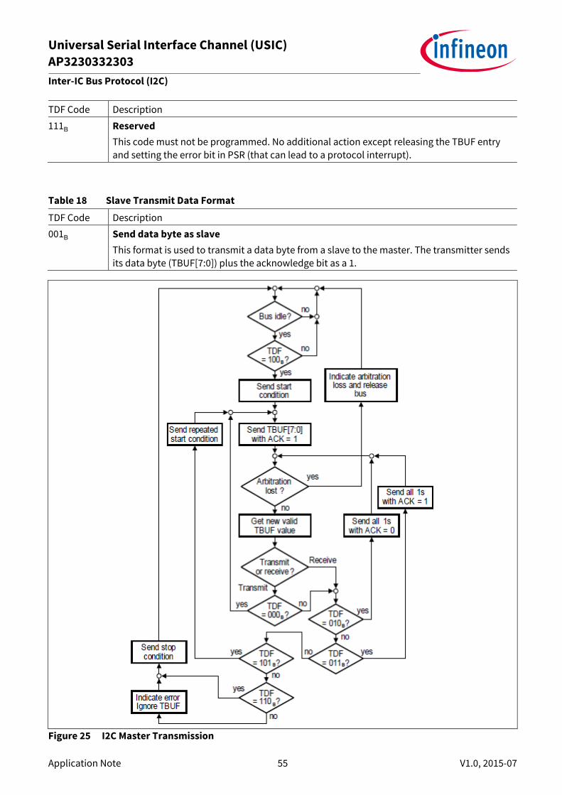
Universal Serial Interface Channel (USIC)
AP3230332303
Inter-IC Bus Protocol (I2C)
Application Note 55 V1.0, 2015-07
TDF Code Description
111B Reserved
This code must not be programmed. No additional action except releasing the TBUF entry
and setting the error bit in PSR (that can lead to a protocol interrupt).
Table 18 Slave Transmit Data Format
TDF Code Description
001B Send data byte as slave
This format is used to transmit a data byte from a slave to the master. The transmitter sends
its data byte (TBUF[7:0]) plus the acknowledge bit as a 1.
Figure 25 I2C Master Transmission

Universal Serial Interface Channel (USIC)
AP3230332303
Inter-IC Bus Protocol (I2C)
Application Note 56 V1.0, 2015-07
4.4 XMC Lib Implementation: Master to Slave mode
This example demonstrates how to use the USIC for an I2C communication in a full-duplex mode.
The I2C protocol is used to implement a counter using the onboard LEDs. The LEDs display the binary
numbers from 1 to 15 continuosly.
The communication of data is established between the USIC module as a Master to the slave IO Expander
(PCA9502) of the COM_ETH_V1 board.
The example is made for the XMC4500 and uses channel 0 of the USIC slice 1, PORT 2.14 and PORT 5.8.
4.4.1 Configuration
The first step is to configure USIC channel with the I2C protocol.After this operation, the configuration of the
baudrate used for the communication is mandatory.
The I2C protocol needs the SDA and SCL pins to be configured:
SDA (Serial Data) contains the data for the communication
SCL ( Serial Clock) is mandatory for I2C because it is a synchronous communication protocol
XMC_USIC_CH_t *i2c = XMC_I2C1_CH0;
XMC_I2C_CH_CONFIG_t i2c_cfg =
{
.baudrate = 100000U,
};
Table 19 Input/output pins for I2C Master to Slave mode
Input/Output pins Function pin Port Driver (IOCRxPC)
SDA USIC1_CH0.DOUT0 P2.14 ALT 2 (open drain)
SCL USIC1_CH0.SCLKOUT P5.8 ALT 2 (open drain)
4.4.2 Initialization
The I2C is initialized with three operations:
First, set the baudrate
Second, select the inputs from the multiplexer of USIC input stage for both pins
Third, switch the USIC channel to the I2C protocol
XMC_I2C_CH_Init(i2c, &i2c_cfg);
XMC_I2C_CH_SetInputSource(i2c, XMC_I2C_CH_INPUT_SDA , USIC1_C0_DX0_P2_14);
XMC_I2C_CH_SetInputSource(i2c, XMC_I2C_CH_INPUT_SCL , USIC1_C0_DX1_P5_8);

Universal Serial Interface Channel (USIC)
AP3230332303
Inter-IC Bus Protocol (I2C)
Application Note 57 V1.0, 2015-07
XMC_I2C_CH_Start(i2c);
4.4.3 Function implementation
The first step of the implementation is to start the Master of the I2C communication. The start command is
forwarded to the slave address. In this example, the address of the slave is the IO Expander (PCA9502) of the
COM_ETH_V1 board address.
The code waits until the ACK is recognized and then clears the ACK flag:
#define COM_PCA9502_ADDRESS (0x98)
XMC_I2C_CH_MasterStart(i2c, COM_PCA9502_ADDRESS, XMC_I2C_CH_CMD_WRITE);
while((XMC_I2C_CH_GetStatusFlag(i2c) & XMC_I2C_CH_STATUS_FLAG_ACK_RECEIVED)
== 0U){}
XMC_I2C_CH_ClearStatusFlag(i2c, XMC_I2C_CH_STATUS_FLAG_ACK_RECEIVED);
Now the I2C is tested with a transmission from Master to the Slave containing information about the slave
plus some dummy data. This is done in order to be sure that the channel is ready.
Again, it is best to wait until ACK is recognized before proceeding to clear the ACK flag:
typedef enum PCA9502_REGADDR {
IO_DIR = 0xA << 3,
IO_STATE = 0xB << 3,
IO_INTE = 0xC << 3,
IO_CTRL = 0xE << 3
} PCA9502_REGADDR_t;
XMC_I2C_CH_MasterTransmit(i2c, IO_DIR);
while((XMC_I2C_CH_GetStatusFlag(i2c) & XMC_I2C_CH_STATUS_FLAG_ACK_RECEIVED)
== 0U){}
XMC_I2C_CH_ClearStatusFlag(i2c, XMC_I2C_CH_STATUS_FLAG_ACK_RECEIVED);
XMC_I2C_CH_MasterTransmit(i2c, 0xffU);
while((XMC_I2C_CH_GetStatusFlag(i2c) & XMC_I2C_CH_STATUS_FLAG_ACK_RECEIVED)
== 0U){}
XMC_I2C_CH_ClearStatusFlag(i2c, XMC_I2C_CH_STATUS_FLAG_ACK_RECEIVED);
Now that the I2C is tested, the LEDs and counter can be setup:
uint8_t counter = 0;
uint8_t io_state1 = 0;
uint8_t received_data;
while(counter < 0xFF)

Universal Serial Interface Channel (USIC)
AP3230332303
Inter-IC Bus Protocol (I2C)
Application Note 58 V1.0, 2015-07
{
io_state1 = ~counter;
counter++;
XMC_I2C_CH_MasterRepeatedStart(i2c, COM_PCA9502_ADDRESS,
XMC_I2C_CH_CMD_WRITE);
while((XMC_I2C_CH_GetStatusFlag(i2c) & XMC_I2C_CH_STATUS_FLAG_ACK_RECEIVED)
== 0U){}
XMC_I2C_CH_ClearStatusFlag(i2c, XMC_I2C_CH_STATUS_FLAG_ACK_RECEIVED);
XMC_I2C_CH_MasterTransmit(i2c, IO_STATE);
while((XMC_I2C_CH_GetStatusFlag(i2c) & XMC_I2C_CH_STATUS_FLAG_ACK_RECEIVED)
== 0U){}
XMC_I2C_CH_ClearStatusFlag(i2c, XMC_I2C_CH_STATUS_FLAG_ACK_RECEIVED);
XMC_I2C_CH_MasterTransmit(i2c, io_state1);
while((XMC_I2C_CH_GetStatusFlag(i2c) & XMC_I2C_CH_STATUS_FLAG_ACK_RECEIVED)
== 0U){}
XMC_I2C_CH_ClearStatusFlag(i2c, XMC_I2C_CH_STATUS_FLAG_ACK_RECEIVED);
XMC_I2C_CH_MasterRepeatedStart(i2c, COM_PCA9502_ADDRESS,
XMC_I2C_CH_CMD_READ);
while((XMC_I2C_CH_GetStatusFlag(i2c) & XMC_I2C_CH_STATUS_FLAG_ACK_RECEIVED)
== 0U){}
XMC_I2C_CH_ClearStatusFlag(i2c, XMC_I2C_CH_STATUS_FLAG_ACK_RECEIVED);
XMC_I2C_CH_MasterReceiveNack(i2c);
while((XMC_I2C_CH_GetStatusFlag(i2c) &
(XMC_I2C_CH_STATUS_FLAG_RECEIVE_INDICATION |
XMC_I2C_CH_STATUS_FLAG_ALTERNATIVE_RECEIVE_INDICATION)) == 0U){}
XMC_I2C_CH_ClearStatusFlag(i2c, XMC_I2C_CH_STATUS_FLAG_RECEIVE_INDICATION |
XMC_I2C_CH_STATUS_FLAG_ALTERNATIVE_RECEIVE_INDICATION);
The last step is to receive the data from the buffer of Rx channel.
received_data = XMC_I2C_CH_GetReceivedData(i2c);
At the end it is mandatory to stop the I2C Master channel:
XMC_I2C_CH_MasterStop(i2c);

Universal Serial Interface Channel (USIC)
AP3230332303
Revision History
Application Note 59 V1.0, 2015-07
5 Revision History
Current Version is V1.0, 2015-07
Page or Reference Description of change
V1.0, 2015-07
Initial Version

Published by
Infineon Technologies AG
81726 Munich, Germany
© 2015 Infineon Technologies AG.
All Rights Reserved.
Do you have a question about any
aspect of this document?
Email: [email protected]
Document reference
Legal Disclaimer THE INFORMATION GIVEN IN THIS APPLICATION NOTE (INCLUDING BUT NOT LIMITED TO CONTENTS OF REFERENCED WEBSITES) IS GIVEN AS A HINT FOR THE IMPLEMENTATION OF THE INFINEON TECHNOLOGIES COMPONENT ONLY AND SHALL NOT BE REGARDED AS ANY DESCRIPTION OR WARRANTY OF A CERTAIN FUNCTIONALITY, CONDITION OR QUALITY OF THE INFINEON TECHNOLOGIES COMPONENT. THE RECIPIENT OF THIS APPLICATION NOTE MUST VERIFY ANY FUNCTION DESCRIBED HEREIN IN THE REAL APPLICATION. INFINEON TECHNOLOGIES HEREBY DISCLAIMS ANY AND ALL WARRANTIES AND LIABILITIES OF ANY KIND (INCLUDING WITHOUT LIMITATION WARRANTIES OF NON-INFRINGEMENT OF INTELLECTUAL PROPERTY RIGHTS OF ANY THIRD PARTY) WITH RESPECT TO ANY AND ALL INFORMATION GIVEN IN THIS APPLICATION NOTE.
Information For further information on technology, delivery terms and conditions and prices, please contact the nearest Infineon Technologies Office (www.infineon.com).
Warnings Due to technical requirements, components may contain dangerous substances. For information on the types in question, please contact the nearest Infineon Technologies Office. Infineon Technologies components may be used in life-support devices or systems only with the express written approval of Infineon Technologies, if a failure of such components can reasonably be expected to cause the failure of that life-support device or system or to affect the safety or effectiveness of that device or system. Life support devices or systems are intended to be implanted in the human body or to support and/or maintain and sustain and/or protect human life. If they fail, it is reasonable to assume that the health of the user or other persons may be endangered.
www.infineon.com
Trademarks of Infineon Technologies AG AURIX™, C166™, CanPAK™, CIPOS™, CIPURSE™, CoolGaN™, CoolMOS™, CoolSET™, CoolSiC™, CORECONTROL™, CROSSAVE™, DAVE™, DI-POL™, DrBLADE™, EasyPIM™, EconoBRIDGE™, EconoDUAL™, EconoPACK™, EconoPIM™, EiceDRIVER™, eupec™, FCOS™, HITFET™, HybridPACK™, ISOFACE™, IsoPACK™, i-Wafer™, MIPAQ™, ModSTACK™, my-d™, NovalithIC™, OmniTune™, OPTIGA™, OptiMOS™, ORIGA™, POWERCODE™, PRIMARION™, PrimePACK™, PrimeSTACK™, PROFET™, PRO-SIL™, RASIC™, REAL3™, ReverSave™, SatRIC™, SIEGET™, SIPMOS™, SmartLEWIS™, SOLID FLASH™, SPOC™, TEMPFET™, thinQ!™, TRENCHSTOP™, TriCore™.
Other Trademarks Advance Design System™ (ADS) of Agilent Technologies, AMBA™, ARM™, MULTI-ICE™, KEIL™, PRIMECELL™, REALVIEW™, THUMB™, µVision™ of ARM Limited, UK. ANSI™ of American National Standards Institute. AUTOSAR™ of AUTOSAR development partnership. Bluetooth™ of Bluetooth SIG Inc. CAT-iq™ of DECT Forum. COLOSSUS™, FirstGPS™ of Trimble Navigation Ltd. EMV™ of EMVCo, LLC (Visa Holdings Inc.). EPCOS™ of Epcos AG. FLEXGO™ of Microsoft Corporation. HYPERTERMINAL™ of Hilgraeve Incorporated. MCS™ of Intel Corp. IEC™ of Commission Electrotechnique Internationale. IrDA™ of Infrared Data Association Corporation. ISO™ of INTERNATIONAL ORGANIZATION FOR STANDARDIZATION. MATLAB™ of MathWorks, Inc. MAXIM™ of Maxim Integrated Products, Inc. MICROTEC™, NUCLEUS™ of Mentor Graphics Corporation. MIPI™ of MIPI Alliance, Inc. MIPS™ of MIPS Technologies, Inc., USA. muRata™ of MURATA MANUFACTURING CO., MICROWAVE OFFICE™ (MWO) of Applied Wave Research Inc., OmniVision™ of OmniVision Technologies, Inc. Openwave™ of Openwave Systems Inc. RED HAT™ of Red Hat, Inc. RFMD™ of RF Micro Devices, Inc. SIRIUS™ of Sirius Satellite Radio Inc. SOLARIS™ of Sun Microsystems, Inc. SPANSION™ of Spansion LLC Ltd. Symbian™ of Symbian Software Limited. TAIYO YUDEN™ of Taiyo Yuden Co. TEAKLITE™ of CEVA, Inc. TEKTRONIX™ of Tektronix Inc. TOKO™ of TOKO KABUSHIKI KAISHA TA. UNIX™ of X/Open Company Limited. VERILOG™, PALLADIUM™ of Cadence Design Systems, Inc. VLYNQ™ of Texas Instruments Incorporated. VXWORKS™, WIND RIVER™ of WIND RIVER SYSTEMS, INC. ZETEX™ of Diodes Zetex Limited.
Last Trademarks Update 2014-07-17
Edition 2015-07
AP32303