united states patent us - nasa · us. patent oct. 18,2005 sheet 1 of 8 us 6,956,230 b1 i 600 i pn...
TRANSCRIPT
(12) United States Patent Gharib et al.
(54) INTEGRATED PARTICLES SENSOR FORMED ON SINGLE SUBSTRATE USING FRINGES FORMED BY DIFFRACTIVE ELEMENTS
(75) Inventors: Morteza Gharib, San Marino, CA (US); Dominique Fourguette, Los Angeles, CA (US); Darius Modarress, Los Angeles, CA (US); Frederic Taugwalder, Altadena, CA (US); Siamak Forouhar, Pasadena, CA (US)
(73) Assignee: California Institute of Technology, Pasadena, CA (US)
Subject to any disclaimer, the term of this patent is extended or adjusted under 35 U.S.C. 154(b) by 544 days.
( * ) Notice:
This patent is subject to a terminal dis- claimer.
(21) Appl. No.: 09/838,344
(22) Filed: Sep. 15, 2000
Related U.S. Application Data (60) Provisional application No. 601154,486, filed on Sep. 17,
1999, and provisional application No. 601154,487, filed on Sep. 17, 1999.
(51) Int. C1.7 ................................................ GOlN 21/49 (52) U.S. C1. ....................... 250/574; 3561336; 3561441;
731865.5; 731705 (58) Field of Search .................... 356135, 49, 335-342,
3561354, 28, 442; 731865.5, 147, 705; 2501550, 237 G, 222.2, 224, 573, 574
Divemng Fringes
(io) Patent No.: (45) Date of Patent:
US 6,956,230 B1 *Oct. 18,2005
(56) References Cited U.S. PATENT DOCUMENTS
3,216,318 A * 1111965 Gaffard ....................... 353197 3,548,655 A * 1211970 Rudd ........................ 356128.5 4,373,807 A 211983 Gouesbet 4,896,098 A * 111990 Haritonidis et al. ........ 3241663 4,948,257 A 811990 Kaufman et al. 5,052,228 A * 1011991 Haritonidis 731705 5,160,976 A 1111992 Carr et al. 5,199,298 A * 411993 Ng et al. ................... 73154.01 5,327,218 A * 711994 Igaki 3561499 5,453,837 A 911995 Naqwi et al. 5,680,211 A * 1011997 Kaneda et al. .............. 3561499 5,701,172 A * 1211997 Azzazy ........................ 356128 5,835,217 A * 1111998 Medecki ..................... 3561521 5,998,782 A * 1211999 Koyama et al. 2501222.2 6,249,351 B1 * 612001 de Groot .................... 3561512
* cited by examiner Primary Examiner-Jay Patidar (74) Attorney, Agent, or F i r m C i s h & Richardson P.C. (57) ABSTRACT
Integrated sensors are described using lasers on substrates. In one embodiment, a first sensor forms a laser beam and uses a quartz substrate to sense particle motion by interfer- ence of the particles with a diffraction beam caused by a laser beam. A second sensor uses gradings to produce an interference. In another embodiment, an integrated sensor includes a laser element, producing a diverging beam, and a single substrate which includes a first diffractive optical element placed to receive the diverging beam and produce a fringe based thereon, a scattering element which scatters said fringe beam based on particles being detected, and a second diffractive element receiving scattered light.
24 Claims, 8 Drawing Sheets
tiqh Co/lecbng Area ,/
https://ntrs.nasa.gov/search.jsp?R=20080005038 2018-09-08T11:40:09+00:00Z

U S . Patent Oct. 18,2005 Sheet 1 of 8 US 6,956,230 B1
I I
600 p n
Light Collectrng Area
#
Diverging fringes 0'
FIG. 7

U S . Patent Oct. 18,2005 Sheet 2 of 8 US 6,956,230 B1
150 140 130 720 I10 700 90 80 70 60 50 -50 50
FIG. 2

U S . Patent Oct. 18,2005 Sheet 3 of 8
h 8
f Og
m h
f cb m h
/
US 6,956,230 B1

U S . Patent Oct. 18,2005 Sheet 4 of 8 US 6,956,230 B1
FIG. 4
U S . Patent Oct. 18,2005
0
Sheet 5 of 8 US 6,956,230 B1
FIG. 5
U S . Patent Oct. 18,2005 Sheet 6 of 8 US 6,956,230 B1
FIG. 6A

U S . Patent Oct. 18,2005 Sheet 7 of 8 US 6,956,230 B1
FIG. 68

U S . Patent Oct. 18,2005 Sheet 8 of 8 US 6,956,230 B1
FIG. 7

US 6,956,230 B1 1 2
INTEGRATED PARTICLES SENSOR FORMED ON SINGLE SUBSTRATE USING
FRINGES FORMED BY DIFFRACTIVE ELEMENTS
CROSS-REFERENCE TO RELATED APPLICATIONS
FIG. 7 shows an integrated optical sensor based on a phased Doppler technique.
DETAILED DESCRIPTION The present application teaches a special miniaturized and
integrated optical sensor probe for measuring wall shear stress in aerodynamic and hydrodynamic flows for example. As described herein, the system also provides structure which is highly minaturizable, and which can be formed within a housing of a special type that enables the use of the
lo sensor in harsh environments. Moreover, the system in is non-intrusive and non-invasive. The center of the probe’s volume may be located very close to the surface being measured, e.g. as close as 100 microns to the surface. Moreover, the sensor as described herein may be configured in a way, as described herein, that may require less calibra- tion.
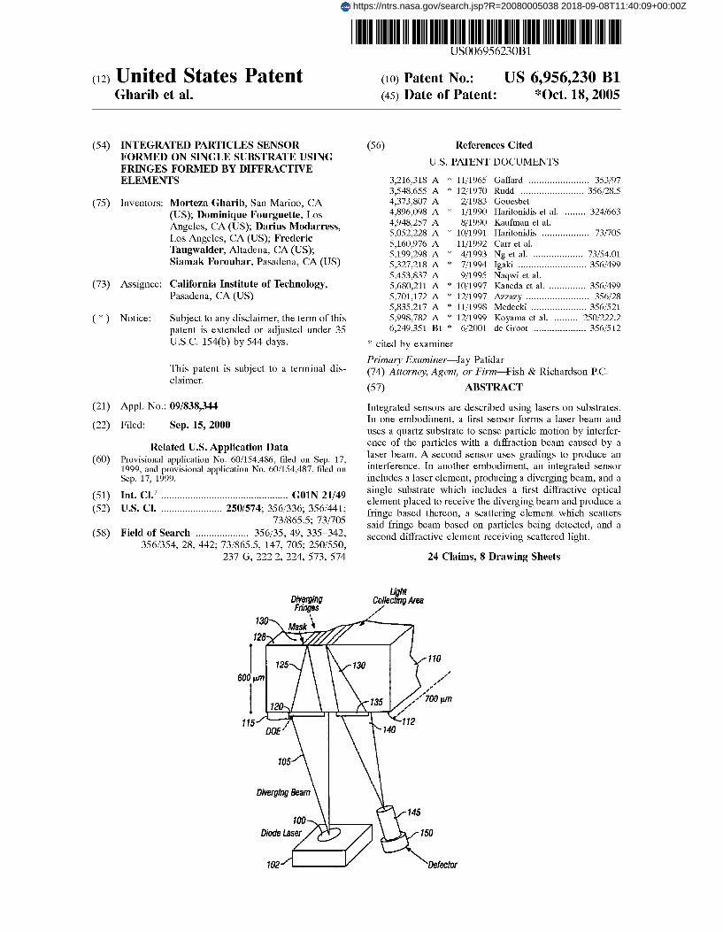
A schematic of the sensor is shown in FIG. 1. A diode laser 100 is formed on a substrate 102. The diode laser
specified angle. The output beam is shaped, for example, into two, parallel very high aspect ratio ellipses. The beam is coupled toward a transparent substrate, e.g., a quartz substrate 110 which forms an optical assembly. The quartz
It is often desirable to obtain different kinds of informa- substrate may have a size, for example, of 6oo microns thick 25 and 700 microns square on a side. The quartz substrate 110 tion about particles.
One kind of information is about shear stress. An existing includes a metal film 115 formed thereon, e,g,, a film formed method of detecting wall shear stress puts a heated wire or of chromium or The metal film is processed to element in the flow to be detected. The rate of cooling of the form specified openings therein, Optical slits are formed in element provides a measure of the wall shear stress. Other an area 120 of the metal film, arranged to form a diffractive similar sensors, which Sense other Parameters, are also 30 optical element. The slits can be fabricated by etching the known. metal from the thin film in a specified pattern.
However, this system by itself has certain problems. The The light exiting from the diffractive optical element 120 techniques may be intrusive, meaning that they may effect forms a two-dimensional, linearly diverging optical fringe the rate of flow. The techniques can be affected by contami- pattern 125. The optical fringe pattern can, for example, nants in the flow. For example, certain contaminants may 35 simply include diverging fringes. The fringe pattern may be deposit on the heated element and cause the heated element ofthe type shown in FIG. 2 where the pattern width is on the to react differently. These techniques can also change the order of 25 microns, and the position is on the order of 90 characteristics of the sensor; hence requiring calibration. microns for the main part of the fringe, with the edges of the
conventional optics. However, this results in a bulky setup, The fringe 125 impinges on a mask 130 which is formed and setup that is highly susceptible to vibration. Moreover, on the second surface 128 of the quartz substrate 110. the size of such a setup may cause difficulty in allowing the The second surface 128 of the quartz substrate is placed system to be effectively used. near the flow to be measured. Light is scattered off the
Other kinds of probes can be used to detect the size of 45 particles crossing the fringe pattern to form reflected beam particles, and may have similar drawbacks. 130.
Scattered light is also obtained by a second optical window 135 that is formed in the metal film 115. The light is collected through that optical window, via another dif-
so fractive optical element 140 formed on the surface of the quartz element. The scattered light is collected by those elements and focused onto an optical fiber detector 145. An avalanche photodiode 150 can be located at the end of the detector, receiving the light therefrom.
An important feature of system in FIG. 1 is that the sensor element can be fabricated using micro-fabrication technol-
The surface 112 includes the laser “lens” 120, and the collection lens 130,140. The other side 128 of the substrate
60 includes a plurality of slits. In addition, both sides of the substrates include alignment marks, 112 include the align- ment marks 312, 314, which are alignment marks for the electronic beams. The front side 128 includes the alignment marks 316, 318 which are the alignment for the front-to-
The substrate may be fabricated as follows. A quartz substrate of size 2 mmx2 mmx0.5 mm is obtained. The
5 .
This application claims benefit of U.S. Provisional appli- cation No. 601154,486, and No. 601154,487, both filed Sep. 17, 1999.
STATEMENT AS TO FEDERALLY-SPONSORED RESEARCH
U,S, G~~~~~~~~~ may have certain rights in this invention pursuant to DaTa grant number N66001-99-1-8902 and U.S. Navy grant no. N00014-99-1-0297.
The invention described herein was made in the perfor- mance of work under a NASA contract, and is subject to the
contractor has elected to retain title. provisions of Public Law 96-517 (U,S,C, 202) in which the 2o produces a diverging Output beam lo5 which diverges at a
BACKGROUND
Non-intrusive optical techniques may be considered using 4o fringe ending at 130-140 microns.
SUMMARY
The present application teaches integrated optical sensors
One aspect detects and/or measures wall shear stress in for detecting particle details.
flows.
BRIEF DESCRIPTION OF THE DRAWINGS
mese and other aspects will now be described in detail 5s with reference to the accompanying drawings wherein:
FIG, 1 shows a schematic for a first wall stress sensor; OgY. The substrate 110 can be formed as shown in 3.
shows an Optical fringe pattern emitted by the
FIG. 3 shows a details of fabrication of the optical Part; FIG. 4 shows an assembly drawing showing the way in
FIG. 5 shows another embodiment using a common
FIGS. 6A and 6B show two embodiments of integrated
sensor of FIG. 1;
which the elements are held within a housing;
substrate to support the laser and the optical detector.
optical sensors.
65 back transfer.

US 6,956,230 B1 3 4
quartz substrate can be fused silica, for example. The substrate is first evaporatively coated with a thin film of chromium using evaporation. The result in structure is then coated with polymethylmetachrylate or PMMA.
formed as two different openings, e.g., a first window 320
of slits 325 are formed to the side of that window. These can be 1-2 microns wide, and 500 microns long. The slits have 10 micron separations from one another, and may be sepa- rated by 5 microns from the window 320. The slits and
locations to receive the scattered light from the particles at the point 610. The phase shift of the detectors is proportional to the particle size at the point 610. An on-chip or off processor or controller may receive the signals from the
6B shows an embodiment in which
produces an Output 652. The diode laser Output 652 is allowed to diverge onto a curved grating 654, which is blocked in its center shown as 656.
The grating 654 redirects the light 652 into two separated light beams 660, 662, which are separated by the blocked
Slits 130 are opened in the front side 128, This can be 5 photodetectors and the particle size.
which is 100 microns wide and 500 microns long, Aplurality fringes in space are formed. A sing1e ended diode 650
Optical window pattern can be Opened in the PMMA e-beam lithography. The chromium may be portion 656, The two light beams 660 and 662 are directed
to intersect 3 millimeters off the surface at the point 664, A separate laser 668 produces an IMAX beam 670. As in the wet edged in the open areas to form better openings.
Thereafter, the surface is coated with a thick layer of FIG. 6A embodiment, photodetectors 680, 682 detect the photoresist in order to protect the surface. The back side 112 scattered light and use the scattered light to find particle size. is also coated with photoresist. The front side alignment Another embodiment shown in FIG, 7 uses a phased marks are used to form front side holes and open holes in the Doppler technique without the technique using the IMAX photoresist using an optical mask and UV exposure. The beam. The same structure of the laser 650 and curved grating surface is then coated with metal for liftoff. The metal is 2o 654 forming the LDA beams intersecting above the surface removed using E-beam alignment marks. All of the photo- is defined. Detectors 700,710 are located on an arm extend- resist can also be removed. ing above the surface to receive the beam. This technique
A PMMA layer is then deposited on the bottom of works best for particle sizes close to the laser wavelength. substrate 112. Two different diffractive optical elements are As in the other embodiments, the scattered light gathered formed in the PMMA layer. The PMMA laser lens 120 is 25 by the two detectors exhibits a phase shift that is propor- formed which is 200 microns wide 500 microns long. The PMMA collection lens 135 is formed that is 400 microns Although only a few embodiments have been defined in wide 500 microns long. These are formed using E-beam lithography and developed using acetone. 3o What is claimed is:
The sensing element is then formed and mounted in a housing 400. The housing 400 includes all of the structure therein, including the diode laser and optical receiver.
This system can produce significant advantages. In addition, modifications in this system are contemplated. For 35 example, a diffractive optical element can be used in place of the optical window 320 in order to collect the scattered light more efficiently.
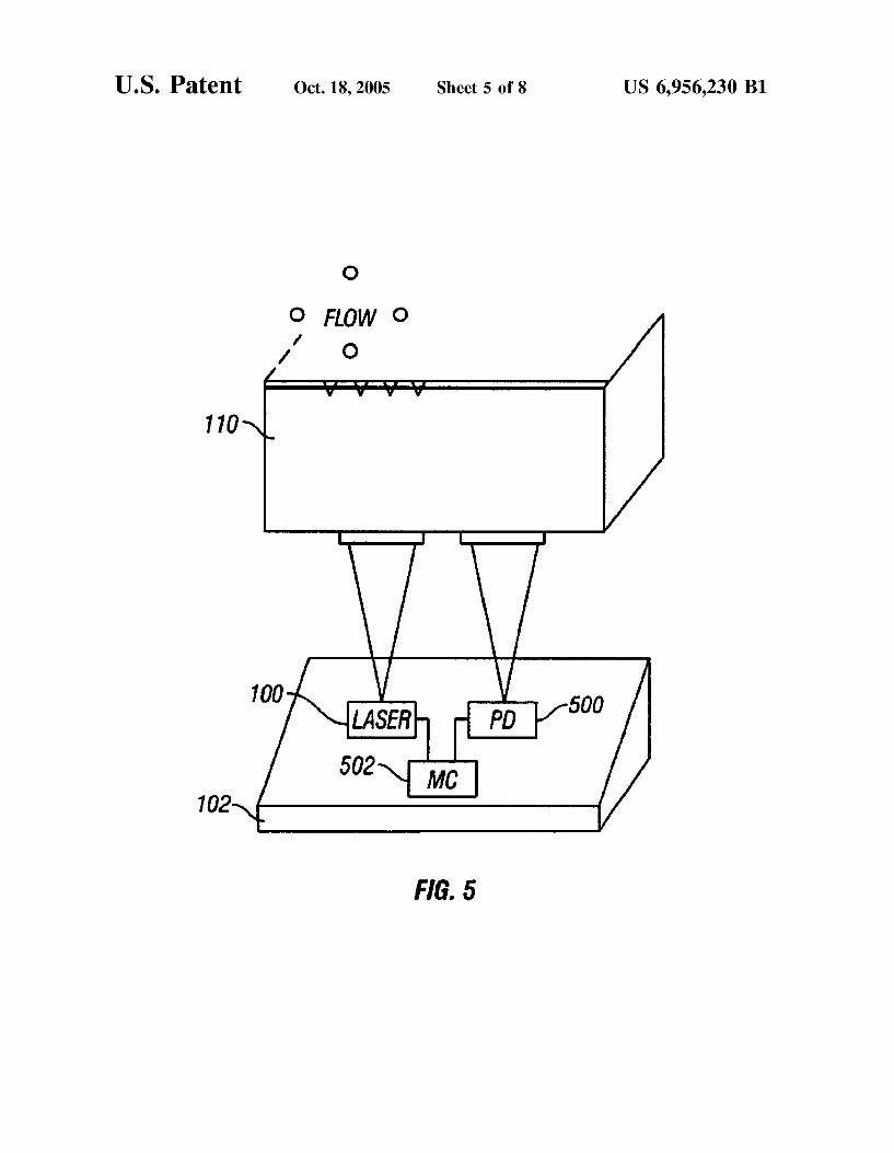
In another embodiment, shown in FIG. 5, the detector is mounted directly on the substrate 102. This avoids the use of 4o fibers, and reduces the parts count. In this embodiment, both the laser 100, and photodiode 500 are mounted on a single substrate 102. A controller 502 may also be mounted on the substrate. The controller may control both the laser 100 and 3. A Sensor as in claim 2, further comprising a second the photodiode 500. For example, the controller can instruct 45 surface, opposite said first surface, including a pattern the laser what and when to emit. It can receive information formed thereon which receives particles crossing the pattern, from the photodiode, and interpret it in view of timing and light crossing the particles being collected as said information sent to the laser. scattered light.
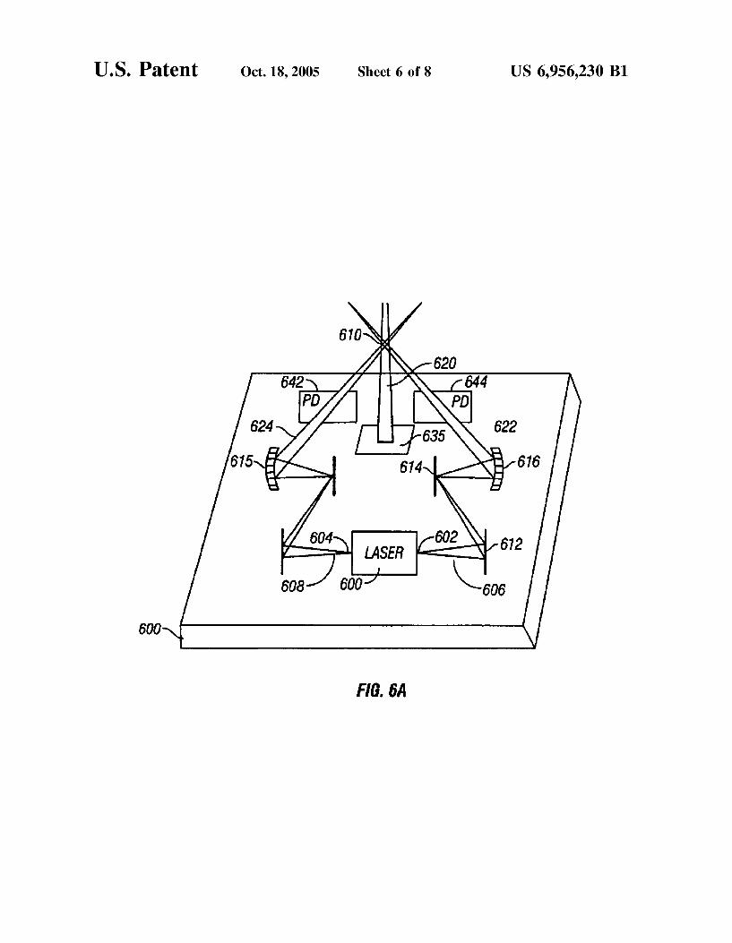
Another embodiment which forms a fiber optic particle 4. A sensor as in claim 1, further comprising a detector, probe is shown in FIGS. 6A and 6B. A diode laser is used so receiving said scattered light, and producing a signal indica- along with curved gratings and detectors. FIG. 6A shows a tive of a property of particles being detected. configuration with a laser 600 emitting along both sides 602 5. A sensor as in claim 4, further comprising a housing, and 604. The two-sided emission provides laser output arms wherein said laser element, said single substrate, and said 606, 608. Beam 606 is reflected by mirrors 612, 614, and detector are coupled within said housing. coupled to a curved grating 616. Beam 608 is correspond- 55 6. A sensor as in claim 1, wherein said substrate is a ingly coupled to grating 618. The outputs 622, 624 of substrate formed of a quartz. gratings 616, 618 are recombined off the surface at a point 7. Asensor as in claim 1, wherein a dimension of each side 610. The point 610, for example, can be 3 millimeters over of said quartz substrate is less than 1000 microns. the surface of the substrate 600. A fringe pattern is formed 8. Asensor as in claim 6, wherein said quartz substrate has by the recombination. 60 a first surface with said first and second diffractive optical
The fringe pattern is centered on a second laser beam, elements formed thereon and a second surface with diverg- called the IMAX beam, that has been created by a second ing fringes which is placed in an area of light collection. laser source 635. The IMAX beam provides information on the size of the particle and as such is a particle-sizing beam 620. 65 contact with a source of particles;
Light is scattered by the particles and received by pho- todetectors 642,644, which are mounted on the substrates in
tional to the phase particle size.
detail above, other modifications are possible,
1. A sensor, comprising: a laser element, producing a diverging beam; and a single substrate, including a first diffractive optical
element placed to receive the diverging beam and to produce a fringe beam based thereon, a mask with openings placed to receive the fringe beam from the first diffractive optical element and to interface with particles being detected which scatter said fringe beam, and a second diffractive element receiving scattered light.
2. A Sensor as in claim 1, wherein said single substrate includes a first surface which includes both said first and second diffractive optical elements.
9. A method of measuring particles, comprising: placing a first surface of a transparent substrate into
illuminating said particles with a laser via a diffractive optical element on a second surface of said substrate to
US 6,956,230 B1 5 6
form interference fringes and receiving scattered light first optical element receiving said laser beam from said from said particles via a second diffractive element; and laser diode, and a second of said optical elements receiving
monitoring said received light to determine information collected light. about said particles. 16. A sensor as in claim 15, wherein said diffractive
10. A method as in claim 9, wherein said diffractive 5 optical elements are formed from PMMA layers on the
17. A sensor as in claim 14, wherein said optical sensor
elements are formed by depositing PMMA on the surface of the substrate.
11. A method as in claim 9, wherein said substrate is formed of quartz.
alignment marks on opposite sides of the substrate. 13. A method as in claim 12, wherein said alignment
marks are formed as positive structures on one side, and lack of positive structures on the other side.
substrate,
includes an avalanche photodiode.
12, A method as in claim 9, further comprising forming 10 18. A method Of particles, comprising: illuminating particles with laser light via a series of slits
detecting interference with said fringe pattern as detecting
14. An integrated shear stress sensor, comprising: 19. A method as in claim 18 wherein said detecting a housing; comprises extracting shear stress information from the inter- a laser diode coupled to said housing in a location to emit ference.
light; 20. Amethod as in claim 18, further comprising directing a sensing element, formed by a transparent substrate, 2o an additional laser beam to the particles to detect a size of
having a first surface adjacent said laser diode to the particles. receive illumination therefrom and a second surface 21. A method as in claim 18, wherein said illuminating adjacent a top portion of said housing to sense particle comprises forming two beams, and recombining said two movement; and beams to form said fringe pattern.
an optical sensor, also coupled to said housing, coupled zs 22. Amethod as in claim 21, wherein said two beams are adjacent to said substrate to receive collected light formed by a laser producing two output beams. therefrom; and 23. A method as in claim 21, wherein said two beams are
optical slits on the second side of the substrate forming a formed by a single grating with a blocked Part.
which form a fringe pattern; and
particle flow.
fringe pattern in an area of said second side of said 24. A method as in claim 18, wherein said detecting substrate, said fringe pattern interfering with said par- 30 comprises detecting light in two locations, and determining ticles. a phase shift therebetween.
15. A sensor as in claim 14, wherein said first surface of said substrate includes two diffractive optical elements, a * * * * *