unit - iii unit objectivechettinadtech.ac.in/storage/11-12-12/11-12-12-11-01-50...unit - iii unit...
TRANSCRIPT

Computer Architecture – Unit 3 :
Computer Arithmetic, Pipeline and Vector Processing
UNIT - III
Unit objective
� To know computer arithmetic using addition and subtraction
� Multiplication algorithms
� Division algorithms
� Floating-point arithmetic operations
� Decimal arithmetic operations
� Pipelining as a means for executing machine instructions concurrently
� Various hazards that cause performance degradation in pipelined
processor and means for mitigating their effect,
� Hardware and software implications of pipelining,
� Influence of pipelining on instruction set design and performance
consideration for the pipelining
Unit Introdution
The ALU performs arithmetic and logical operations on data. All other
components of computer system bring data into ALU for processing. The
information handled in a computer is generally divided into “words”, each
consisting of fixed number of bits for e.g., if the words handled by a
microcomputer are 32 bits in length, the ALU would have to be capable of
performing arithmetic operations on 32 bits words. Data are presented to the
ALU in registers and the results of an operation are stored in registers. The
control unit coordinates the operations of the ALU and the movement of the
data in and out of the ALU. Most computers have one or more registers
called accumulator, or general purpose registers. The accumulator is the

Computer Architecture – Unit 3 :
Computer Arithmetic, Pipeline and Vector Processing
basic register containing one of the operands during operations in ALU. If
the computer is instructed to add, the number stored in the accumulator is
augends and the addend will be located and these operands (addend &
augends) are added up and the result is storedd back in the accumulator. The
original augends will be lost in accumulator after addition.
In this unit, we discuss in detail the concept of pipelining, which is used in
the modern computer to achieve high performance. We begin by explaining
the basics of pipelining and how it can lead to improved performance. Then
we examine a machine instructions feature that facilitates pipelined
execution, and we show that choice of instructions and instructions
sequences can have significant effect on performance. Pipelined
organization requires sophisticated compilation techniques, and optimizing
compilers have been developed for this purpose. Among other thinks, such
compilers rearrange the sequence of operations to maximize the benefits of
pipelined executions
Arithmetic operations
Arithmetic instruction in digital computers manipulates data to produce
result necessary for the solution of computational problem. These
instructions perform arithmetic calculation and are responsible for bulk of
activity in processing data in a computer. The 4 basic arithmetic operations
are
1) Addition
2) Subtraction
3) Multiplication
4) Division
From the 4 basic operations it is possible to formulate other arithmetic
functions and solve scientific problem by means of numerical analysis
methods.
An arithmetic processor is the part of a processor unit that executes
arithmetic operation. The data type assumed to reside in processor register
during the execution of an arithmetic instruction is specified in the definition
of the instruction. An arithmetic instruction is specified in the definition of
the instruction. An arithmetic instruction may specify binary or decimal data
and in each case the data may be fixed point or floating point form. Fixed-
point number may represent integers or fractions. Negative number may be

Computer Architecture – Unit 3 :
Computer Arithmetic, Pipeline and Vector Processing
in signed-magnitude or signed complement form.
A step-by-step procedure involved in solving any problem is called an
algorithm. In this chapter we develop the various arithmetic algorithms and
show the procedure for implementing them with digital hardware. We
consider the addition, subtraction, multiplication and division for the
following types of data.
1. Fixed-point (data) binary data in signed-magnitude representation.
2. Fixed-point binary data in signed 2’s complement representation.
3. Floating-point binary data
4. Binary-coded decimal (BCD) data
Fixed point ALU
The following fig shows the most widely used ALU design. It is intended to
implement multiplication and division using one of the sequential digit by
digit shifts and add! Subtract algorithms. Three one word registers are used
for operand storage: Accumulator AC, the Multiplier Quotient register MQ
and the data register DR. AC and MQ are organized as a single register
AC.MQ capable of left and right shifting. The main additional data
processing capability is provided by the parallel adder that receives inputs
from AC and DR and places its results in AC. The MQ register is so called
because it stores the multiplier during the multiplication operation, and
quotient during the division operation. DR stores the multiplicand or the
divisor while the result is stored in AC.MQ.
In many instances DR serves as a memory buffer register to store data
addressed by the instruction address field ADR.

Computer Architecture – Unit 3 :
Computer Arithmetic, Pipeline and Vector Processing
Fig. Block diagram of fixed point ALU.
Bit-Sliced ALU
It is possible to construct an entire fixed point ALU on a single IC chip
especially if the word size m is kept fairly small ex: 4 or 8 bits. Such an rn-
bit ALU can be designed to be expandable in that k copies of the ALU chip
can be connected to form a single ALU capable of processing km-bit
operands directly. The resulting array like circuit is called bit sliced because
each component chip processes an independent slice of m bits from each km
bit operand. Bit sliced ALU’ s have advantage that any desired word size or
even, several different word sizes can be handled by selecting the
appropriate number of components (bit slices) to use.
The following Fig. shows a 16-bit ALU can be constructed from 4-bit ALU
slices. The data buses and registers of the individual slices are placed to
increase their sizes from 4 to 16 bits. The control lines that select and
sequence the operation to be performed are connected to every slice, so that

Computer Architecture – Unit 3 :
Computer Arithmetic, Pipeline and Vector Processing
all slices execute the same operation in step with one another. Each slice
performs the same operation on a different 4-bit part (slice) of the input
operands, and produces only the corresponding part of the results. The
required control lines are derived from an external control unit which is
usually micro programmed. Certain operations require information to be
exchanged between slices. For ex if a shift operation is to be implemented
then each slice must send a bit to and receive a bit from left or right
neighbor’s .Similarly when performing addition the carry bits m Data in (16
bits) Data out (16 bits).
Fig Bit-Sliced ALU.
INTEGER REPRESENTATION-FIXED POINT
The numbers used in digital machines are represented using binary digits 0
and 1. The storage element called flip flops can hold these digits. Group of
flip flops forms a register in computer systems.
E.g. the number 41 can be represented as
o o 1 0 1 0 0 1 [8 bit representation]
Thus if a register contains 8 bits, a signed binary number in the system will
have 7 magnitude bits or integer and a single sign bit and the system is
called signed magnitude binary integer system.
E.g. +18 = 00010010
-18 = 10010010
Signed-Magnitude Representation
The positive and negative numbers are differentiated by treating the most
significant bit in the word as a sign bit. If the sign bit is 0, the number is
positive. If the sign bit is 1, the number is negative

Computer Architecture – Unit 3 :
Computer Arithmetic, Pipeline and Vector Processing
Drawbacks
1. Addition and subtraction requires both the sign bit and magnitude bits to
be considered.
2. Two representation for zero (0)
+0 — >00000000
-o —> 10000000
Two’s Complement Representation
In two’s complement system, forming the 2’s complement of a number is
done by subtracting that number from 2N
E.g. Representation of —4
In Sign-magnitude 11 0 0
In 1 ‘s complement 1 0 11
In 2’s complement 11 0 0
Advantages:
i. only one arithmetic operation is required while subtracting using 2’s
complement notation.
ii. Used in arithmetic applications.
Sign Extensions
It is sometimes desirable to take an n-bit integer and store it in m bits, where
m > n.
to do this,
in sign-magnitude notation,
• simply move the sign bit to the new leftmost position and fill in with zeros.
In 2’s complement notation
• Move the sign bit to the new leftmost position and fill it with copies of
the sign bit.
• For -fve no’s fill it with zeros.
• For -ye no’s fill it with ones.
E.g.

Computer Architecture – Unit 3 :
Computer Arithmetic, Pipeline and Vector Processing
+18 =000 100 10 — 8 bit notation
=0000000000010010 f— l6bitnotationinsignmagnitude
-18 =1110 1110 — 2’s complement 8 bit notation
=111111111101110 — 2’s complement l6bitnotation
Both the sign-magnitude and 2’s complement representation discussed
above are often called as fixed point notation as the decimal point (binary)
read point is fixed and assumed to be to the right of the rightmost digit.
INTEGER ARITHMETIC
Are implemented in the ALU of the processor. As given above, arithmetic
operations are performed on fixed point, floating point and binary coded
decimal data. In both fixed point signed magnitude notation and 2’s
complement notation, the sign bit is treated as the same as the other bits.
Full Adder
A full adder is a combinational circuit that forms the arithmetic sum of three
input bits. It consists of three inputs and two outputs. Two of the input
variables denoted by x and y, represent the two significant bits to be added.
The third input, z represents the carry from the previous lower significant
position. The two outputs are designated by symbols S for sum and C for
carry. The binary variable S gives the value of the least significant bit of the
sum. The binary variable C gives the output carry.
Fig Full Adder Circuit.

Computer Architecture – Unit 3 :
Computer Arithmetic, Pipeline and Vector Processing
In the truth table, when all input bits are 0’s, the output is 0. The S output is
equal to 1 when only one input is equal to 1 or when all three inputs are
equal to 1. The C output has a carry of 1 if two or three inputs are equal to 1.
Hardware Implementations
When k-map is drawn for S and C, we have
Thus the logic expression for Si can be implemented with a 3 input XOR
gate and logic expression for C01(C) is implemented with a two-level
AND—OR logic circuit.
A cascaded connection of n full adder can be used to add two n-bit numbers.
Since the carry propagates or ripples, this cascade of full adders is called n-
bit ripple carry-adder.
To perform the subtraction operation X-Y on 2’s complement numbers X
and Y, 2’s complement of Y is added to X. Overflow occur when the signs

Computer Architecture – Unit 3 :
Computer Arithmetic, Pipeline and Vector Processing
of the two operands are the same and if the sign of the result is different.
i) If the overflow occurs, the ALU must signal this fact so that no attempt is
made to use the result. ii) Overflow can occur whether or not there is a carry.
4-bit binary adder
The digital circuit that performs the arithmetic sum of two bits and a
previous carry is called a Full adder. The digital circuit that generates the
arithmetic sum of two binary numbers of any lengths is called the binary
adder.
The binary adder circuit can be constructed with full adder circuits
connected in cascade. Here the output carry from one full adder can be
connected to the input carry of the next full adder. The augends bits of X and
the addend bits of Y are designated by subscript numbers from right to left
as shown below. The carries are connected in chain through to Full adders.
The input carry to the binary adder is the C0 and the output carry to the
binary adder is the S outputs of the full adders generate the required sum
bits.
The n-bit binary adder requires n-full adders. The n-data bits for the X inputs
are from one register R1 and n-data bits for the Y input come fmm another
register R2. The sum can be transferred to the third register or one of the
source register. (R1 or R2)
Fig -Bit Binary Adder
4-bit Binary adder I sub tractor

Computer Architecture – Unit 3 :
Computer Arithmetic, Pipeline and Vector Processing
The subtraction of binary numbers can be done by means of complements.
The subtraction of X and Y i.e. X-Y can be done by taking the 2’s
complement of Y and adding it to X. The 2’s complement can be obtained
by taking the l’s complement and adding 1 to it. The addition and
subtraction can be combined in one circuit by including the XOR gate with
each full adder. The mode input M controls the operation. When M =0 the
circuit is an adder, when M = 1 the circuit is a subtractor. Each XOR agate
receives input M and one of the inputs of Y. When M =0 we have Y 0 = Y.
The full adder receives the value of Y. the input carry is 0, and the circuit
performs the X plus Y.
When M = 1 we have Y ® 1 = and C0 = 1. The Y inputs are all
complemented and 1 is added through the input carry. The circuit performs
X plus 2’s complement of Y.
For unsigned numbers this gives the X — Y if X >=Y or the 2’ s
complement (Y—X) if x<Y.
For signed numbers the result is (X-Y) provided there is no overflow.
Fig Binary Adder/ Sub tractor
4-bit binary arithmetic circuit
The 4-bit arithmetic circuit has four full adders constitutes a 4-bit adder and
4 MUX for choosing different operation. There are two 4-bit inputs A and B
and 4-bit output D. The 4 inputs from X go directly to the A input of the
binary adder. Each of the 4 inputs of the Y are connected to the data input of
the MUX. The MUX data inputs also receive the complement of Y. The

Computer Architecture – Unit 3 :
Computer Arithmetic, Pipeline and Vector Processing
other two data inputs are connected to logic 0 and logic 1. The 4 MUX are
controlled by selection inputs S0 and S1. The input carry goes to the carry
input of the PA in the LSB. The other carries are connected from one stage
to another.
The output of the binary adder is calculated from the following arithmetic
sum.
D=X+Y+C.
X - 4 bit binary number at A inputs.
Y - 4 bit binary number at B inputs.
C - Input carry which can be 0 or 1.
By controlling the value of Y with two selection inputs S0 and S1 and
making C1, equal to 0 or 1 it is possible to generate 8 possible arithmetic
operations.
Addition:
When S1S0 =00, the value of Y is applied to the B input of the adder.
If =0, the output D =X +Y. If C1 =1 then the output is D =X +Y +1. Both
cases perform addition micro operation with or without carry.
Subtraction:
When S0S1 =01. The complemented value of Y is applied to the B input of
the adder. If C. =0 the output D=X-f(Comp)Y. This is equivalent to D =X—
Y-1. If C =1 then the output is D =X -+(Comp)Y+1 .This produces X plus
the 2’s complement of Y, which is equivalent to X—Y. Both cases perform
the subtraction micro operation with or with out borrow
When S1S0=10 the input from the B are neglected all 0’s are applied to the
B input the output becomes D =X +1 when C in =1
When S1S0 =11 all l’s are inserted in to B input of the adder to produce the
Decrement operation. D =X-1, when C1 =0. This is because the number with
all l’s equal to 2’s complement of 1. (2’s complement of 0001 = 1111).
Adding a number X to the 2’s complement of 1 produce D=X-1.
When C in=1 then D =X-1 +1 =X

Computer Architecture – Unit 3 :
Computer Arithmetic, Pipeline and Vector Processing
Fig 4-Bit Binary Arithmetic Circuit.
Addition & Subtraction of Signed Numbers
We designate the magnitude of two number by X and Y. When signed
number are added or subtracted we find that there are 8 different conditions
to consider, depending on the sign of the number and the operation
performed. These conditions are listed in the following table 3 1 (1st
column). The other columns show the actual operation to be performed with
the magnitude of the number. The last column is needed to prevent —0.
When two equal numbers are subtracted the result should be –0 not -0.

Computer Architecture – Unit 3 :
Computer Arithmetic, Pipeline and Vector Processing
Addition Algorithm:
a) When the signs of X and Y are identical add the two magnitudes and
attach the sign of X to the result.
b) When the signs of X and Y are different compare the magnitude and
subtract the smaller number from the larger. Choose the sign of the result as
X if X > Y or complement of the sign of X if X <Y.
c) If the two magnitudes are equal, subtract Y from X and make the result
positive.
Hardware Implementation:
To implement the two arithmetic operations with hardware it is first
necessary that the two numbers be stored in register. Let X and Y be two
register that hold the magnitude of the number and Xs and Ys be two flip
flop that hold the corresponding signs. The result of operation may be
transferred to a 3rd register. However a saving is achieved by transferring
the result into X and Xs. Thus X and Xs together form an accumulator
register.
Consider now the hardware implementation of the algorithm above.
1) First a parallel adder is needed to perform the micro operation X +Y.
2) A comparator circuit is needed to establish if X >Y, X =Y or X <1
3) Two parallel subtractor circuits are needed to perform the micro operation
X - Y and YX
4) The sign relation can be determined from an XOR gate with Xs and Ys
input.
This procedure required a magnitude comparator, an adder, and two
subtractors. However a different procedure can be found that require less
equipment.
a) First we know that subtraction can be accomplished by means of
complement and addition.
b) The result of a comparison can be determined from the end carry after the
subtraction.
The following fig. shows the hardware implementation of the addition and
subtraction operation. It consists of register X and Y and sign flip flop Xs
and Ys. Subtraction is done by adding X to the 2’s complement of Y. The
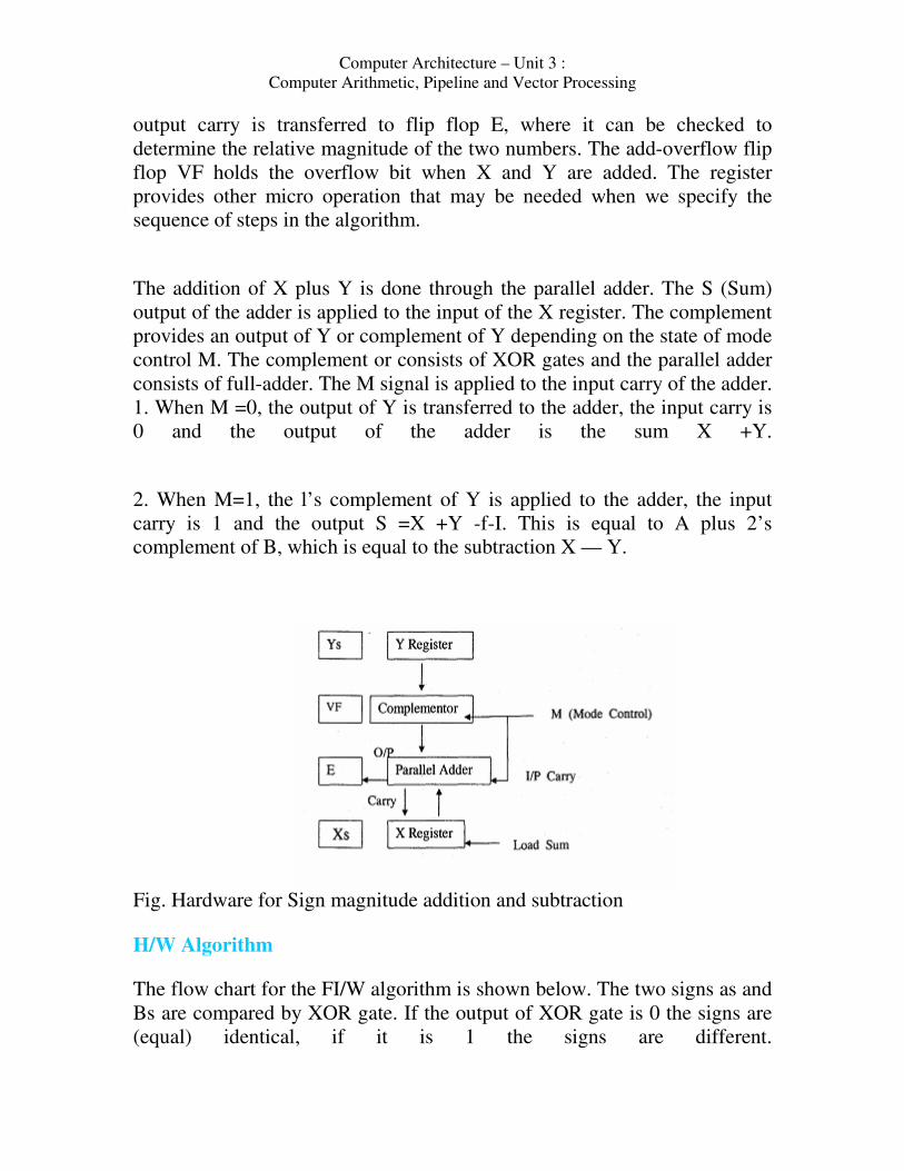
Computer Architecture – Unit 3 :
Computer Arithmetic, Pipeline and Vector Processing
output carry is transferred to flip flop E, where it can be checked to
determine the relative magnitude of the two numbers. The add-overflow flip
flop VF holds the overflow bit when X and Y are added. The register
provides other micro operation that may be needed when we specify the
sequence of steps in the algorithm.
The addition of X plus Y is done through the parallel adder. The S (Sum)
output of the adder is applied to the input of the X register. The complement
provides an output of Y or complement of Y depending on the state of mode
control M. The complement or consists of XOR gates and the parallel adder
consists of full-adder. The M signal is applied to the input carry of the adder.
1. When M =0, the output of Y is transferred to the adder, the input carry is
0 and the output of the adder is the sum X +Y.
2. When M=1, the l’s complement of Y is applied to the adder, the input
carry is 1 and the output S =X +Y -f-I. This is equal to A plus 2’s
complement of B, which is equal to the subtraction X — Y.
Fig. Hardware for Sign magnitude addition and subtraction
H/W Algorithm
The flow chart for the FI/W algorithm is shown below. The two signs as and
Bs are compared by XOR gate. If the output of XOR gate is 0 the signs are
(equal) identical, if it is 1 the signs are different.

Computer Architecture – Unit 3 :
Computer Arithmetic, Pipeline and Vector Processing
1. For an addition operation the identical signs dictate that the magnitude be
added.
2. For subtraction operation different signs dictate that magnitude be
subtracted. EX - X +Y, Where EX - Reg that combines E and X. The carry
in E after the addition constitutes an overflow if it is equal to 1.
3.The value of E is transferred into the add-overflow flip-flop VF.
4. The two magnitude are subtracted if the two signs are different for an
addition operation or identical for subtract operation. The magnitude is
subtracted by adding X to the number is subtracted so VF is cleared to 0.
5. A 1 in E indicates that X � Y and the number in X is the correct result. If
this number is zero the sign X must be made positive to avoid a negative
zero.
6. A zero in E indicates that X <Y. For this case it is necessary to take the
2’s complement of the value in X. This operation can be done with the micro
operation X - X + 1. However we assume that the X register has circuits
function micro operation complement and increment. So the 2’s complement
is obtained from these two micro operations. In other paths of the flow
charts the sign of the result is the same as the sign of X, so no change in X is
required. When X <Y the sign of the - result is the complement of the
original sign of X. It is then necessary to complement X to obtain the correct
sign. The final result is found in register X and its sign in Xs. The value in
VF provides an overflow indication. The final value of E is immaterial.

Computer Architecture – Unit 3 :
Computer Arithmetic, Pipeline and Vector Processing
Fig. Flowchart for add and subtract operation
Addition and subtraction with 2’s complement data
The left most bit of a binary number represents assign bit 0- positive, 1 -
negative. If the sign bit is 1 the entire number is represented in 2’s
complement form.
Thus Ex: -433 are represented as 00100001 and -33 as 11011111. Note that
11011111 is the 2’s complement of 00100001 and vice versa.
The addition of two numbers in signed 2’s complement form consists of
adding the number with the sign bits treated the same as the other bits of the
number. A carryout of the sign-bit position is discarded. The subtraction
consists of first taking 2’s complement of the subtrahend and then adding it
to the minuend.
When two numbers of n digits each are added and the sum occupies n+l
digits. We say that an overflow occurred. An overflow can be detected by
inspecting the last two carries out of the addition. When the two carries are
applied to the XOR gate the overflow is detected when the output of the gate
is equal to 1.
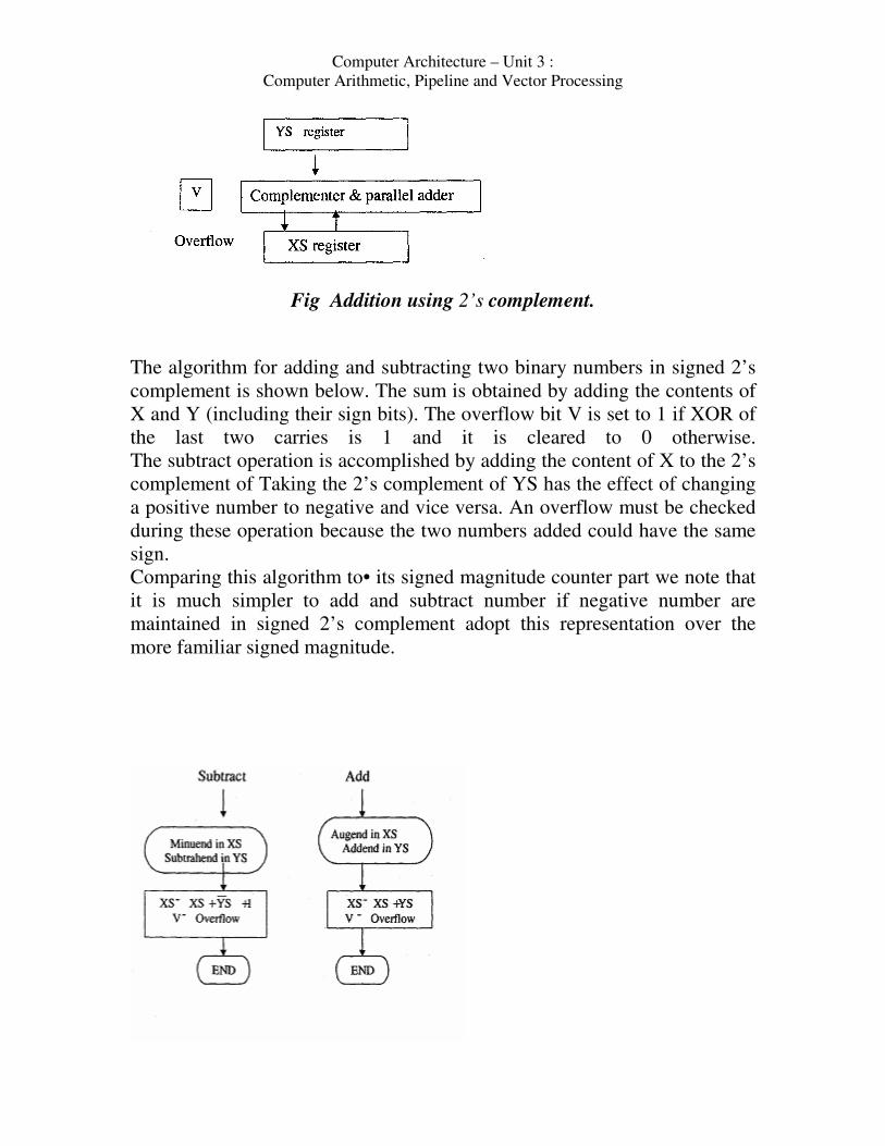
The register configuration for hardware implementation is shown in the
figure below. This is same as the figure above but the sign bits are not
separated from the rest of the register. We name the X register X5
(Accumulator) and the Y register Y. The left most bit in X and ‘‘represents
the sign bits of the number. The two sign bits are added or subtracted
together with the other bits in the parallel adder. The overflow flip-flop V is
set to I if there is an overflow. The output carry in this case is discarded.
Computer Architecture – Unit 3 :
Computer Arithmetic, Pipeline and Vector Processing
Fig Addition using 2’s complement.
The algorithm for adding and subtracting two binary numbers in signed 2’s
complement is shown below. The sum is obtained by adding the contents of
X and Y (including their sign bits). The overflow bit V is set to 1 if XOR of
the last two carries is 1 and it is cleared to 0 otherwise.
The subtract operation is accomplished by adding the content of X to the 2’s
complement of Taking the 2’s complement of YS has the effect of changing
a positive number to negative and vice versa. An overflow must be checked
during these operation because the two numbers added could have the same
sign.
Comparing this algorithm to• its signed magnitude counter part we note that
it is much simpler to add and subtract number if negative number are
maintained in signed 2’s complement adopt this representation over the
more familiar signed magnitude.

Computer Architecture – Unit 3 :
Computer Arithmetic, Pipeline and Vector Processing
Fig. Algorithm for addition and subtraction of 2’s complement
Design of Fast adders :
Carry Propagation
The addition of two binary numbers in parallel implies that a litlle bits of the
augend and the addend are available for computation at the same time.
The parallel adders are ripple carry types in which the carry output of each
full adder stage is connected to the carry input of the next higher-order stage.
The sum of carry outputs of any stage cannot be produced until the input
carry occurs. This lead to a time delay in the addition process.
The carry propagation delay for each full adder is the Time& from the
application of the input carry until the output carry occurs, assuming that the
P and Q inputs are present. Full adder 1 in fig. given below cannot produce
a potential carry output until a carryout is applied. I.e. the input carry to the
least significant stage has to ‘ripple’ through all the adders before the final
sum is produced. A cumulative delay through all of the adder stages is a
‘worst-case’ addition time. The total delay can vary, depending on the
carries produced by each stage. If two numbers are added such that no
carriers occurs between stages, the add time is simply the propagation time
through a single full adder from the application of the data bits on the inputs
to the occurrence of a sum output.
Fig .four bit adder using full adder

Computer Architecture – Unit 3 :
Computer Arithmetic, Pipeline and Vector Processing
The Look Ahead Carry Adder
In parallel adder, the speed with which an addition can be performed is
limited by the time required for the carries to propagate or ripple through all
of the stages of adder. One method of speeding up this process is by
culminating this ripple carry delay is called Look- Ahead Carry addition and
is based on two functions of the full adder called the carry generate and the
carry propagate function
Fig. Full Adder Bit Stage Cell
From the full adder circuit,
Now the expression for the carry out C0. Of each full adder stage for the
four bit
Propagate P = x1 +y
For first full addeer
C1 =G0+C0P0

Computer Architecture – Unit 3 :
Computer Arithmetic, Pipeline and Vector Processing
For second full addeer
C2 =G+CP
=G1-4-P1(G0+C0P0) [: c=G0+P0c0}
C2 = + G0P + C0P1P0
Similarly
C3 =G,+CP
=G, +(G1 +G0P +C0P1P0)P2
= G2 + G1P2 + G0P1P2 + C0P2P1P6
In all the above expressions, the carry output for each full -adder stage is
dependent only on the initial input cany (C0), its G0 and P0 functions and
the G and P functions of the preceeding stages.
Since, each of the G and P functions can be expressed in terms of the x and y
inputs to the full adders, all of the output carries are immediately available
and the adder circuit need not have to wait for a carry to ripple through all of
the stages before a final result is achieved. Thus the look ahead carries
technique speeds up the addition process.
Fig. bit adder using Carry Look Ahead Logic.
In general, the final expression for any carry variable is
C, =G + PG1 +PPG12 + + P1P PG0+ P1P P0G0

Computer Architecture – Unit 3 :
Computer Arithmetic, Pipeline and Vector Processing
All carries can be obtained three gate delays after the input signals X, Y and
C0 are applied because only one gate delay is needed to develop all P and
G1 signals, and followed by two gate delays in the AND-OR circuit for
C1÷1 (See fig. 3.12 Full-Adder-Bit stage cell)
After a further XOR gate delay, all sum bits are available. Therefore,
independent of n, the n-bit addition process requires only four gate delays.
Delays in Carry Look ahead adder
Fig 16 bit Carry-Look ahead adder built from 4-bit adders.
In carry-look ahead 4-bit adder, all carries are obtained three gate delays
after the input signals X, Y and C0 are applied because one gate delay is
needed to develop all P1 and signals followed by two gate delays in the
AND-OR circuit for C11. After a further XOR gate delay, all sum bits are
available. Therefore independent of n, the n-bit addition process requires
only four gate delays.
In the above fig. 3.14, the carryout C4 from the low order adder is available
3 gate delays after the input operands X, Y and C0 are applied to the 16 bit
carry look ahead adder.
C8 is available after a further 2 gate delays, C12 is available after a further 2
gate delays and C16 is available after a further 2 gate delays.
(i.e.) C16 is available after a total of
(3>2) + 3 9 gate delays.

Computer Architecture – Unit 3 :
Computer Arithmetic, Pipeline and Vector Processing
If a ripple carry adder is used, C16 is available only after 31 gate delays for
S15 and 32 gate delays for C16.
Higher-Level generate and propagate functions
By using Higher-Level block generate and propagate functions, it is possible
to use the look ahead approach to develop the carries C4, C8, C12 in parallel
in a higher-level carry look ahead circuit.
In Fig. 3.14, 16 bit Carry Look Ahead Adder
P1 =P3P2P1P0 &
G01’
P0
G =G3 +PGr2 +P3P2G1 +P3P2P1G0
and
C16 can be C16 =G +PG +PPG +PPPj1G +PPP’PC0
Gate-delays when higher level block generate and propagate functions are
used .Carry generated internally by the 4-bit adder blocks are not needed
because they are generated by the higher-level carry look ahead circuits.
G & P are produced after 3 gate delays after the generation of G and P.
The delay in developing the carries produced by the carry look ahead
circuits is two gate delays more than delay needed to develop G’ & P and
hence totally 5 gate delays after X, Y and C0 are applied as inputs. Then the
sum is produced after further 3 gate delays (S15 after 2 gate delays when
C12 is available and 1 further gate delay) thus totally 8 gate delays.
Therefore when cascaded 4 bit adder is used, S15 and C16 are available after
10 and 9 gate delays. When higher level carry look ahead adder is used, S15
and C16 are available after 8 and 5 gate delays.
Multiplication of positive numbers

Computer Architecture – Unit 3 :
Computer Arithmetic, Pipeline and Vector Processing
Multiplication of two fixed-point binary numbers in signed-magnitude
representations is done by a process of successive shift and adds operations.
The process consists of looking at successive bits of the multiplier, LSB
first. If the multiplier bit is a I the multiplicand is copied down: otherwise
zeroes are copied down. The number copied down in successive lines are
shifted one position to the left from the previous number finally the number
are added and their sum forms a product.
The sign of the product is determined from the signs of the multiplicand and
multiplier. It they are alike the sign of the product is positive. It they are
different the sign of the product is negative.
Multiplication algorithm using Signed - Magnitude data
1) Instead of providing register to store and add simultaneously as much
binary number as there are bits in the multiplier, it is convenient to provide
an adder for the summation of only two binary numbers and successively
accumulate the partial products in a register.
2) Instead of shifting the multiplicand to the left, the partial product is
shifted to the right, which results in leaving the partial product and the
multiplicand in the required (Position) relations.
3) When the corresponding bit of the multiplier is 0 there is no need to add
all zeros to the partial product since it will not alter its value.
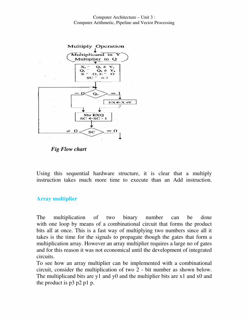
Fig Hardware for multiply Operation

Computer Architecture – Unit 3 :
Computer Arithmetic, Pipeline and Vector Processing
The LSB of X is shifted in to the MSB position of Q., the bit from E is
shifted in to MSB position of X. After the shift, one bit of the partial product
is shifted into Q, passing multiplier bits one position to through right. In this
manner the right most FF in register Q, designated by Q will hold the bit of
the multiplier, which must be inspected next.
H/W algorithm:
Initially
The multiplicand is in Y and the multiplier in Q. their corresponding signs
are
in Y and Q respectively. The signs are compared, and both X and Q are set
to correspond to the sign of the product since a double - length product will
be stored in reg. X and Q register X and E are cleared and the sequence
counter SC is set to a number equal to the number of bits of the multiplier.
We are assuming here that operands are transferred to register from a
memory unit that has words of n bits. Since an operand must be stored with
its sign, one bit of the word will be occupied by the sign and the magnitude
will consists of (n-i) bits.
After the initialization the low order bit of the multiplier in Q is tested if it is
a 1, the multiplicand in Y is added to the present partial product in X. If it is
0 nothing is done. Register EXQ is then shifted once to the right to form the
new partial product. The sequence counter SC is decremented by I and its
new value is checked if it is not equal to zero the process is repeated and the
new partial is formed. The process stops when SC =0 note that the partial
product in X is shifted in to Q one bit at a time and eventually replaces the
multiplier. The final product is available in both X and Q with X holding the
MSBs and Q holding LSBs.
Computer Architecture – Unit 3 :
Computer Arithmetic, Pipeline and Vector Processing
Fig Flow chart
Using this sequential hardware structure, it is clear that a multiply
instruction takes much more time to execute than an Add instruction.
Array multiplier
The multiplication of two binary number can be done
with one loop by means of a combinational circuit that forms the product
bits all at once. This is a fast way of multiplying two numbers since all it
takes is the time for the signals to propagate though the gates that form a
multiplication array. However an array multiplier requires a large no of gates
and for this reason it was not economical until the development of integrated
circuits.
To see how an array multiplier can be implemented with a combinational
circuit, consider the multiplication of two 2 - bit number as shown below.
The multiplicand bits are y1 and y0 and the multiplier bits are x1 and x0 and
the product is p3 p2 p1 p.

Computer Architecture – Unit 3 :
Computer Arithmetic, Pipeline and Vector Processing
The first partial product is formed by multiplying x0 by y1y0. The
multiplication of two such as x0 and y0 produces a 1 if both bits are 1;
otherwise it produces a product 0. is identical to AND operation and can be
implemented with AND gate. As shown in 3.17, the first partial product is
formed by means of two AND gates.
The second partial product is formed by multiply by x1 by y1y0 and is
shifted one position to the left. The two partial products are added with two
half adder (HA) circuits. Note that LSB of the product does not have to get
through an adder since it is formed by output of first AND gate.
Fig- bit by 2 - bit array multiplier
A combinational circuit binary multiplier with more bits can be constructed
in a similar fashion. A bit of the multiplier is AND ed with each bit of
multiplicand in as many levels as there are bits in a multiplier.
For j multiplier bits and k multiplicand bits, we need j x k AND gates and (j-
1) k-bit adders to produce a product of j + k bits.
Signed Operand Multiplication
These topics discuss multiplication of 2’s complement signed operands,
generating a double length product.
Booth Multiplication Algorithm

Computer Architecture – Unit 3 :
Computer Arithmetic, Pipeline and Vector Processing
Booth algorithm gives a procedure for multiplying binary integers in signed
2’s complement representation. It operates on the fact that string of 0’s in the
multiplier requires no addition but just shifting, and a string of 1 ‘s in the
multiplier from bit weight 2k to weight 2 can be treated as (22m). For
example, the binary number 001110 (+14) has a string of l’s from 2 to 21
(k3m=1) the number can be represented as 2k-H_2m = 2 - 21 = 16—2 = 14
Therefore Multiplication M x 14 where M — multiplicand and 14 the
multiplier can be done as (M x 2 - M x 21). Thus the product can be
obtained by shifting the binary multiplicand M four times to the left and
subtracting M shifting left once.
As in all multiplication schemes, booth algorithm requires examination of
the multiplier bits and shifting of the partial product. Prior to the shifting, the
multiplicand may be added to the partial product, subtracted from the partial
product or left unchanged according the following rules
1) The multiplicand is subtracted from the partial product upon encountering
the first least significant 1 in a string of l’s in the multiplier
2) The multiplicand is added to the partial product upon encountering the
first 0 (provided that there was a previous 1 in a string of 0’s in the
multiplier.
3) The partial product does not change when the multiplier bit is identical to
the previous multiplier bit
The algorithm works for positive (or) negative multiplier in 2’s comp
representation. This is because a negative multiplier ends with a string of l’s
and the last operation will be a subtraction of the appropriate weight
Ex:- Multiplier equals to -14 in 2’s complement form — 110010 and is
treated as 24+2221 = -14
The H/W implementation of Booth algorithm require the register
configuration as shown below. This is similar to 11/W fig above except that
the sign bits are not separated from the rest of the register. To show this
difference we rename the set, X. Y and Q as XC, YR and QR respectively.
Qn designates the LSI3 of multiplier in reg. QR. An extra FF Qn+1 is
appended to QR to facilitate a double bit inspection of the multiplier

Computer Architecture – Unit 3 :
Computer Arithmetic, Pipeline and Vector Processing
Fig. Hardware for Booth algorithm
Fig. Booth Algorithm for multiplication of signed -2’s complementer
The flow chart for Booth algorithm is shown above in Fig. 3.19, XR and
appended bit Q are initially cleared to 0 and the sequence counter SC is set
to a number n equal to the number of bits in the multiplier. The two bits of
the multiplier in Q and Q are inspected. If the two bits are equal to 10, it
means that the first un a string of l’s has been Q Q+1 encountered. This
requires a subtraction of the multiplicand from the partial product in XR.
Where the two bits are equal, the partial product does not change. An
overflow can’t occur because the addition and subtraction of the
multiplicand follow each other. As a consequence, the two numbers that are
added always have opposite signs, a condition that excludes an overflow.
The next step is to shift right the partial product and the multiplier (including
Bit Q11) this is an arithmetic shift (Asher) operation which shift XR and YR
to the right and leaves the sign bit in XR unchanged. The sequence counter
(SC) is decremented and the computational loop is repeated n times.

Computer Architecture – Unit 3 :
Computer Arithmetic, Pipeline and Vector Processing
A numerical example of Booth algorithm for n =5 is given, it shows the
step-by-step multiplication of (-9) x (-13)=117 note that the multiplier in QR
is negative and that, the multiplicand in YR is also negative. The 10-bit
product appends in XR and QR and is positive. The final value of Q the
original sign bit of the multiplier should not be taken as part of the product
Booth Algorithm Advantages
(i) It handles both positive and negative multipliers uniformly.
(ii) It achieves some efficiency in the number of additions required when the
multiplier has a few large blocks of l’s.
(iii) The speed gained by skipping l’s depends on the data.
Fast Multiplication
there is two techniques for speeding up the multiplication operation.
(i) Bit Pair Recoding of Multipliers
(ii) Carry Save Addition of Summands
Bit Pair Recoding of Multipliers
Guarantees that the max number of summands (versions of the multiplicand)
that must be added is reduced by half and is derived from Booth’s Alg.
(i) Group the Booth recoded Multipliers bits in pairs.
(ii) If the Booth recoded multiplier is examined two bits at a time, starting
from the right, it can be rewritten in a form that requires at most one version
of the multiplicand to be added to the partial product for each pair of
multiplier bits.

Computer Architecture – Unit 3 :
Computer Arithmetic, Pipeline and Vector Processing
Carry Save addition of summands
Multiplication of 2 numbers involves the addition of several summands
(partial products). A technique called carry save addition speeds up the
addition process.
In ordinary multiplication process, while adding the summands, the carry
produced by second bit position has to be added with third bit position and
so on. Thus the carry ripple along the rows.
Steps for addition of summands in the multiplication of longer
operands
1. Group the summands into threes and perform carry save addition to
produce S and C vectors in one full adder delay.
2. Group all the S and C vectors into threes and perform carry save addition
to generate further set of S and C vectors in one more full adder delay.
3. Do the step 2 until there are only two vectors remaining.
4. Perform ripple carry addition or carry look ahead addition to produce the
desired product.
Division
Division of two-fixed point binary number in signed magnitude
representation is done by a process of compare, shift and subtract operations.
Binary division is simpler than decimal division because the quotient digits
are either 0 or 1.
Consider an example the divisor Y consists of five bits and the dividend X
of 10 bits. The five MSB bits of the dividend are compared with the divisor.
Since the five bit number is smaller than Y we try again by taking 6 MSB
bits of X and compare this number with Y. The 6 bit number is greater than
Y, so we place a 1 for the quotient bit in the 6th position above the dividend.
The difference is called a partial remainder, because the division could have
stopped here to obtain a quotient of 1 and the remainder is equal to the
partial remainder. The process is continued by comparing a partial remainder
Computer Architecture – Unit 3 :
Computer Arithmetic, Pipeline and Vector Processing
with the divisor. If the partial remainder is greater than or equal to the
divisor, the quotient bit is equal to 1. The divisor is then shifted right and
subtracted from the partial remainder. If the partial remainder is smaller than
the divisor, the quotient bit is 0 and no subtraction is needed. The divisor is
shifted once to the right in any case. The result gives both a quotient and
remainder.
Division Overflow
The division operation may result in a quotient with a overflow, i.e. when
the operation is implemented with hardware this is because the length of the
register is finite and will not hold the number that exceeds the standard
length. The divide overflow condition must be avoided in normal computer
operation because the entire quotient will be too long to transfer into
memory unit that has words of standard length, that is, same as the
lengthofregister.
When the dividend is twice as long as the divisor the condition to overflow
can be stated as follows. A divide-overflow condition occurs if the high
order half bits of dividend constitute a number greater than or equal to the
divisor. Another fact associated with division is the fact that the division
with Zero is avoided. The divide overflow condition takes care of this
condition as well. This occurs because any dividend will be greater than or
equal to a divisor, which is equal to zero. Overflow condition is usually
detected when the special FF is set. We will call it a divide-overflow FF and
label it DVF.
1) The occurrence of divide overflow can be handled in a variety of ways. In
some computer it is the responsibility of the programmer to check if DVF is
set after each (division) divide instruction. They then can branch to a
subroutine that takes a corrective measure such as rescaling the data to avoid
overflow.
2) In some olden computers, the occurrence of divide overflow stopped the
computer and this condition was referred to as divide stop. Stopping the
operation of computer is not recommended because it is time consuming.

Computer Architecture – Unit 3 :
Computer Arithmetic, Pipeline and Vector Processing
The procedure in most computers is to provide an interrupt required, when
DVF is set. The instruction causes the computer to suspend the current
program and branch to a service routine to take a corrective measure.
The best way to avoid a divide overflow is to use floating-point data.
Integer Division (Restoring Method)
When the division is implemented in a digital computer, it is convenient to
change the process slightly instead of shifting the divisor to the right the
dividend or partial remainder, is shifted to the left thus may be achieved by
adding X to the 2’s complement of Y.
The 111W for implementing the division operation is identical to that
required for multiplication. Register is now shifted to the left with 0 inserted
into Q and previous value of E is lost.
Ex:- The divisor is stored in the Y register and the double length dividend is
stored in register X and Q. The dividend is shifted to the left and the divisor
is subtracted by adding its 2’s complement value. The information about the
relative magnitude is available in E. If E 4 it signifies that X�Y. A quotient
bit I is inserted into the Q and the partial remainder is shifted to the left to
repeat the process. If E=O it signifies that X Y so that quotient in Q is 0
(inserted during the shift). The value of Y is then added to restore partial
remainder in X to its previous value. The partial remainder is shifted to the
left and the process is repeated again until all five- quotient bits are formed.
The quotient is in Q and the final remainder is in X.

Computer Architecture – Unit 3 :
Computer Arithmetic, Pipeline and Vector Processing
Fig.Register Configuration
H/w Algorithm
The dividend is in X and Q and the divisor in Y The sign of the result is
transferred to Q to be a part of quotient. A constant is set in to sequence
counter ç to specify the no of bits in a quotient. The operands are transferred
to register from a memory unit that has words to n-bits. Since an operand
must be stored with its sign, one bit of the word will be occupied by the sign
and the magnitude will consists of (n-i) bits.
A divide overflow condition is tested by subtracting divisor in Y from half
of the bits of the dividend stored in X. If X>Y, the divide-overflow FF PY1E
is set and the option is terminated permanently.

Computer Architecture – Unit 3 :
Computer Arithmetic, Pipeline and Vector Processing
Fig Flow chart for divide operation (Restoring Method)
The division of magnitude starts by shifting the dividend in XQ to the left
with the high order bit shifted in to E. If the bit is shifted in to E is 1, we
know that EX B because EX consists of 1 followed by (n-i) bits while Y
consists of only (n-i) bits. In this case Y must be subtracted from LX and i
inserted in to Q for the quotient bit. Since register X is missing the high
order bit of the dividend,(which is in E) its value is EX-2’. Adding to this
value the 2’s complement of Y result is
(EX-2) + (2”-Y) = EX-Y
The carry from this addition is not transferred to E if we want E to remain a
1.
If the shift left option inserts a 0 in to E the divisor is subtracted by adding
its 2’s complement value and the carry is transferred in to E. If E =1, it
signifies that X >Y;_therefore Q is to 1. If E=O, it signifies that X Y and the
original no is restored by adding Y to X. In the later case we leave a Q in Q
(0 was inserted during the shift)
this process is repeated again with register. X holding the partial remainder.

Computer Architecture – Unit 3 :
Computer Arithmetic, Pipeline and Vector Processing
After (n-i) times, the quotient magnitude is formed in register X. The
quotient sign is in Q and sign of the remainder in X is same as the original
sign of the dividend.
In th3 configuration given in fig.
Register M holds the divisor
Register Q holds the dividend at the start of operation.
Register X is initially set to 0.
After division Register Q contains quotient.
Register X contains Remainder
Algorithm
1. Shift X and Q left one binary position
2. Subtract M from A and place the answer back in X
3. If the sign of X is 1, set q0 to 0 and add M back to X (restore X);
otherwise set q0 to 1.
Non Restoring algorithm

Computer Architecture – Unit 3 :
Computer Arithmetic, Pipeline and Vector Processing
Step 1: Do the following n times
1. If the sign of A is 0, shift A and Q left one bit position and subtract M
from A,
otherwise, shift A and Q left and add M to A.
2. If the sign of A is 0, set to 1; otherwise, set to 0.
Step 2: If the sign of A is 1, add M to A
Note: Restore operations are no longer needed and that exactly one add or
subtract operation is performed per cycle.

Computer Architecture – Unit 3 :
Computer Arithmetic, Pipeline and Vector Processing
Floating Point Numbers Representation:
The floating point numbers contains the binary point variable in its position
and hence these numbers are called floating point numbers. Because the
position of the binary point number is variable, it must be given explicitly in
the floating point representation.

Computer Architecture – Unit 3 :
Computer Arithmetic, Pipeline and Vector Processing
If the decimal point is placed to the right of the first significant digit, (non
zero) the number is said to be normalized.
A floating point number consists of sign, mantissa and an exponent.
IEEE Standard for floating point numbers
The IEEE standard describes the floating point representations and the way
in which the four basic arithmetic operations are to be performed on these
floating point operands.
There are two types of representations for floating point numbers.
1. Single Precision
2. Double Precision
Value represented = ± 1 .M x227
In this representation, one bit is needed for the sign of the
number. Since the leading non-zero bit of a normalized binary mantissa must
be a 1, it does not have to be included explicitly in the representation.
Instead of signed exponent E. the value actually stored in the exponent field
is an unsigned integer E’ = E+127. This is called the excess —127 format.

Computer Architecture – Unit 3 :
Computer Arithmetic, Pipeline and Vector Processing
Therefore the range of E’ for normal values is 1 E’ _<254.
This means that the actual exponent E is in the range —126 E 127.
Double Precision
Special Values
When B’ =0, the mantissa M is zero.
Similarly
B’ =255 and M =0, the value 00 is represented where oc is the result of
dividing a normal number by zero.
When E’ =0, and M 0, denormal numbers are represented.
E.g. .±0.M x2126 —* denormal numbers are allowed to represent very small
numbers.
When B’ =255 and M 0, the value represented is Not-a-Number (NaN) -*
result of invalid operation 0/0 sqrt(-1)

Computer Architecture – Unit 3 :
Computer Arithmetic, Pipeline and Vector Processing
Table IEEE 754 Format Parameters
• For exponent values in the range of 1 through 254 for single format and 1
through 2046 for double format, normalized non-zero floating point numbers
are represented.
• The exponent is biased, so that the range of exponents is —126 thro +127
for single format and —1022 through +1023 for double format.
• A normalized number requires a 1 bit to the left of the binary point this bit
is implied giving an effective 24-bit or 53-bit significant.
Exceptions
If a number has the exponent value less than —126 we say underflow has
occurred.
If a number has the exponent value greater than +127, we say overflow has
occurred.
Such conditions are called exceptions, Exception flag is set if underflow,
overflow, divide by zero, in exact or invalid operations occur.
Overflow
When normalized mantissas are added, the sum may contain an overflow
digit. An overflow can be corrected easily by shifting the sum once to the
right and incrementing the exponent.
Underflow
When two numbers are subtracted, the result may contain significant zeros.
Eg.
0.56780 x10⁵
-0.56430 x10⁵
0.00350 x10⁵
a floating point number that has a 0 in the most significant position of the

Computer Architecture – Unit 3 :
Computer Arithmetic, Pipeline and Vector Processing
mantissa is said to have an underflow.
In most computers, a normalization procedure is performed after each
operation to ensure that all results are in a normalized form.
Floating point multiplication and division do not require an alignment of the
mantissa.
Multiplication —* Multiply two mantissa and add exponents.
Division —> Divide the mantissa and subtract exponents
Operations with mantissa are same as in fixed point representation.
Operation performed with exponents are compare and increment (for
aligning the mantissa) add and sub (for multiplication and division) and
decrement (to normalize the result)
Biased Exponent
In this representation, the sign bit is removed from being a separate entity.
The bias is a positive number that is added to each exponent as the floating
point number is formed, so that internally all exponents are positive.
Typically, the bias equals 2k1_1 where k is the number of bits in the binary
exponent.
Advantages
Contains only positive numbers
simple to compare their relative magnitudes without being concerned
with their sign.

Computer Architecture – Unit 3 :
Computer Arithmetic, Pipeline and Vector Processing
Arithmetic operations on floating point numbers
In floating point operations, it is assumed that each floating point number
has a mantissa in signed magnitude representation and biased exponent.
If the exponents differ, the mantissas of floating point numbers must be
shifted with respect to each other before they are added and subtracted.
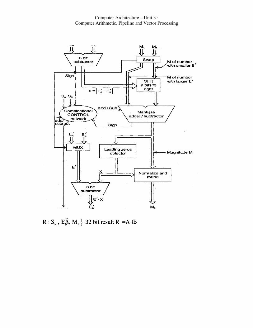
Addition / Subtraction
1. Choose the number with the smaller exponent and shift its mantissa right
a number of steps equal to the difference in exponents.
2. Set the exponent of the result equal to the larger exponent.
3. Perform addition / subtraction on the mantissas and determine the sign of
the result.
4. Normalize the resulting value if necessary
Computer Architecture – Unit 3 :
Computer Arithmetic, Pipeline and Vector Processing

Computer Architecture – Unit 3 :
Computer Arithmetic, Pipeline and Vector Processing
Flow Chart for Floating point Add & Sub.
The flow chart depicts the generalized approach for addition/subtraction of
floating point numbers.
1. Check for zeros
2. Align the mantissas
3. Add or sub the mantissas
4. Normalize the result

Computer Architecture – Unit 3 :
Computer Arithmetic, Pipeline and Vector Processing
Implementation Steps
1. In the figure, the first step is to compare exponents to determine the
number of times the mantissa of the smaller exponent to be shifter.
2. The shift value n is then given to the shifter unit to shift the mantissa of
the smaller number.
3. The sign of the exponent after subtraction determines which is smaller or
which is larger no and thereby to shift the mantissa of the smaller number.
4. The mantissas are added I subtracted. The sign of the result is determined
by combinatorial control network. if E > E’3 then sign is positive or if E <E
then sign is negative.

Computer Architecture – Unit 3 :
Computer Arithmetic, Pipeline and Vector Processing
5. The result is normalized by truncating the leading zeros and by
subtracting E’ by X, the number of leading zeros.
Multiplication
1. Add the exponents and subtract 127.
2. Multiply the mantissas and determine the sign of the result.
3, Normalize the resulting value of necessary.

Computer Architecture – Unit 3 :
Computer Arithmetic, Pipeline and Vector Processing
Fig. Flow Chart for Floating Point Multiplication.
Division

Computer Architecture – Unit 3 :
Computer Arithmetic, Pipeline and Vector Processing
1. Subtract the exponents and add 127.
2. Divide the mantissas and determine the sign of the result.
3. Normalize the resulting value, if necessary.
Fig Flow Chart for Floating Point Division.
Guard bits and Truncation
In 32 bit single precision floating point representation the mantissa bits are
limited to 24 bits including implicit leading 1. But some operations may
result in extra bits called guard bits and these bits should be retained during
the intermediate steps to increase the accuracy in final results.
Similarly, allowing guard bits during intermediate steps results in extended
mantissa. Thus this extended mantissa should be truncated to 24 bits while
generating final results.

Computer Architecture – Unit 3 :
Computer Arithmetic, Pipeline and Vector Processing
There are several ways to truncate
(i) Chopping
(ii) Von-Neumann rounding
(iii) Rounding
(1) Chopping
Chopping is the simplest way to do truncation. I.e. Remove the
guard bits and make no changes in the retained bits.
E.g.
0.b1 b2 b3 000
0.b1 b2 b3 111
are truncated to 0.b1 b 2 b3
Error in chopping ranges from 0 to almost 1 and results in biased
approximation of b position.
(ii) Von-Neumann Rounding
In this method, if the bits to be removed are all 0’s, they are simply
dropped, with no changes to the retained bits.
If any of the bits to be removed are 1, the least significant bit of the
retained bit is set to 1.
Error in this technique is larger than chopping and the
approximation is unbiased and hence results in high probability of
accuracy.
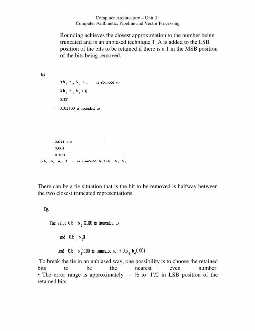
(iii) Rounding Procedure
Computer Architecture – Unit 3 :
Computer Arithmetic, Pipeline and Vector Processing
Rounding achieves the closest approximation to the number being
truncated and is an unbiased technique 1 .A is added to the LSB
position of the bits to be retained if there is a 1 in the MSB position
of the bits being removed.
There can be a tie situation that is the bit to be removed is halfway between
the two closest truncated representations.
To break the tie in an unbiased way, one possibility is to choose the retained
bits to be the nearest even number.
• The error range is approximately — ½ to -I’/2 in LSB position of the
retained bits.

Computer Architecture – Unit 3 :
Computer Arithmetic, Pipeline and Vector Processing
• This rounding technique is the default mode for truncation specified in the
IEEE floating point standard.
PIPELINING
BASIC CONCEPTS
The speed of execution of programs is influenced by many factors.
One way to improve performance is to use faster circuit technology to build
the processor and the main memory. Another possibility is to arrange the
hardware so that more than one operation can be performed at the same
time. In this way, the number of operations performed per second is
increased even though the elapsed time needed to perform any one operation
is not changed. The concept of multiprogramming and explained how it is
possible for I/O transfers and computational activities to proceed
simultaneously. DMA devices make this possible because they can perform
I/O transfers independently once these transfers are initiated by the
processor. Pipelining is a particularly effective way of organizing concurrent
activity in a computer system. The basic idea is very simple. It is frequently
encountered in manufacturing plants, where pipelining is commonly known
as an assembly-line operation. Readers are undoubtedly familiar with the
assembly line used in car manufacturing. The first station in an assembly
line may prepare the chassis of a car, the next station adds the body, and the
next one installs the engine, and so on. While one group of workers is
installing the engine on one car, another group is fitting a car body on the
chassis of another car, and yet another group is preparing a new chassis for a

Computer Architecture – Unit 3 :
Computer Arithmetic, Pipeline and Vector Processing
third car. It may take days to complete work on a given car, but it is possible
to have a new car rolling off the end of the assembly line every few minutes.
Consider how the idea of pipelining can be used in a computer. The
processor executes a program by fetching and executing instructions, one
after the other. Let Fi and Ei refer to the fetch and execute steps for
instruction Ii. Executions of a program consist of a sequence of fetch and
execute steps.
Now consider a computer that has two separate hardware units,
1. Fetching instructions and
2. Executing instructions.
The instruction is fetched by the fetch unit is deposited in an intermediate
storage buffer, B1. This buffer is needed to enable the execution unit to
execute the instruction while the fetch unit is fetching the next instruction.
The results of execution are deposited in the destination location specified
by the instruction. For the purposes of this discussion, we assume that both
the source and the destination of the data operated on by the instructions are
inside the block labeled “Execution unit.”

Computer Architecture – Unit 3 :
Computer Arithmetic, Pipeline and Vector Processing
Fig: Basic idea of instruction pipelining
The computer is controlled by a clock whose period is such that the
fetch and execute steps of any instruction can each be completed in one
clock cycle. Operation of the computer proceeds as shown in the Figure ©.
In the first clock cycle, the fetch unit fetches an instruction I1 (step F1) and
stores it in buffer B1 at the end of the clock cycle. In the second clock cycle,
the instruction fetch unit proceeds with the fetch operation for instruction I2
(step F2). Meanwhile, the execution unit performs the operation specified by
instruction I1, which is available to it in buffer B1 (step E1). By the end of

Computer Architecture – Unit 3 :
Computer Arithmetic, Pipeline and Vector Processing
the second clock cycle, the execution of instruction I1 is completed and
instruction I2 is available. Instruction I2 is stored in B1, replacing I1, which
is no longer needed. Step E2 is performed by the execution unit during the
third clock cycle, while instruction I3 is being fetched by the fetch unit. In
this manner, both the fetch and execute units are kept busy all the time. If the
pattern in Figure © can be sustained for a long time, the completion rate of
instruction execution will be twice that achievable by the sequential
operation depicted in Figure (a).
In summary, the fetch and execute units in Figure (b) constitute a two-stage
pipeline in which each stage performs one step in processing an instruction.
An interstate storage buffer, B1, is needed to hold the information being
passed from one stage to the next. New information is loaded into this buffer
at the end of each clock cycle. The processing of an instruction need not be
divided into only two steps. For example, a pipelined processor may process
each instruction in four steps, as follows:
F Fetch: read the instruction from the memory.
D Decode: decode the instruction and fetch the source operand(s).
E Execute: perform the operation specified by the instruction.
W Write: store the result in the destination location.
Four instructions are in progress at any given time. This means that
four distinct hardware units are needed. These units must be capable of
performing their tasks simultaneously and without interfering with one
another. Information is passed from one unit to the next through a storage
buffer. As an instruction progresses through the pipeline, all the information
needed by the stages downstream must be passed along. For example, during
clock cycle 4, the information in the buffers is as follows:
Computer Architecture – Unit 3 :
Computer Arithmetic, Pipeline and Vector Processing
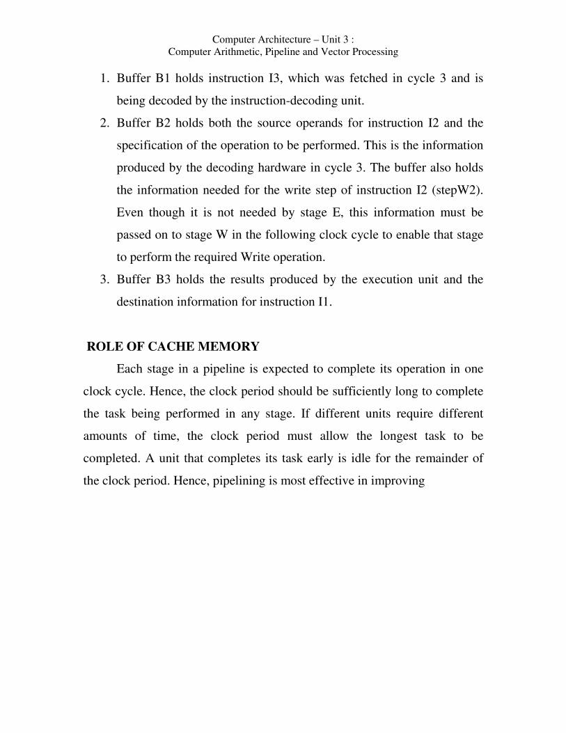
1. Buffer B1 holds instruction I3, which was fetched in cycle 3 and is
being decoded by the instruction-decoding unit.
2. Buffer B2 holds both the source operands for instruction I2 and the
specification of the operation to be performed. This is the information
produced by the decoding hardware in cycle 3. The buffer also holds
the information needed for the write step of instruction I2 (stepW2).
Even though it is not needed by stage E, this information must be
passed on to stage W in the following clock cycle to enable that stage
to perform the required Write operation.
3. Buffer B3 holds the results produced by the execution unit and the
destination information for instruction I1.
ROLE OF CACHE MEMORY
Each stage in a pipeline is expected to complete its operation in one
clock cycle. Hence, the clock period should be sufficiently long to complete
the task being performed in any stage. If different units require different
amounts of time, the clock period must allow the longest task to be
completed. A unit that completes its task early is idle for the remainder of
the clock period. Hence, pipelining is most effective in improving

Computer Architecture – Unit 3 :
Computer Arithmetic, Pipeline and Vector Processing
fig: A 4-stage pipeline
performance if the tasks being performed in different stages require about
the same amount of time. This consideration is particularly important for the
instruction fetch step, which is assigned one clock period in Figure 8.2a. The
clock cycle has to be equal to or greater than the time needed to complete a
fetch operation. However, the access time of the main memory may be as
much as ten times greater than the time needed to perform basic pipeline
stage operations inside the processor, such as adding two numbers. Thus, if
each instruction fetch required access to the main memory, pipelining would
be of little value. The use of cache memories solves the memory access
problem. In particular, when a cache is included on the same chip as the
processor, access time to the cache is usually the same as the time needed to
perform other basic operations inside the processor. This makes it possible
to divide instruction fetching and processing into steps that are more or less

Computer Architecture – Unit 3 :
Computer Arithmetic, Pipeline and Vector Processing
equal in duration. Each of these steps is performed by a different pipeline
stage, and the clock period is chosen to correspond to the longest one.
PIPELINE PERFORMANCE
The pipelined processor completes the processing of one instruction in
each clock cycle, which means that the rate of instruction processing is four
times that of sequential operation. The potential increase in performance
resulting from pipelining is proportional to the number of pipeline stages.
However, this increase would be achieved only if pipelined operation as
depicted in Figure .a could be sustained without interruption throughout
program execution. Unfortunately, this is not the case. For a variety of
reasons, one of the pipeline stages may not be able to complete its
processing task for a given instruction in the time allotted. For example,
stage E in the four-stage pipeline of Figure 8.2b is responsible for arithmetic
and logic operations, and one clock cycle is assigned for this task. Although
this may be sufficient for most operations, some operations, such as divide,
may require more time to complete.
The below figure shows an example in which the operation specified
in instruction I2 requires three cycles to complete, from cycle 4 through
cycle 6. Thus, in cycles 5 and 6, the Write stage must be told to do nothing,
because it has no data to work with. Meanwhile, the information in buffer
B2 must remain intact until the Execute stage has completed its operation.
This means that stage 2 and, in turn, stage 1 are blocked from accepting new
instructions because the information in B1 cannot be overwritten. Thus,
steps D4 and F5 must be postponed as shown.

Computer Architecture – Unit 3 :
Computer Arithmetic, Pipeline and Vector Processing
fig: Effect of an execution operation taking more than one clock cycle
Pipelined operation is said to have been stalled for two clock cycles. Normal
pipelined operation resumes in cycle 7. Any condition that causes the
pipeline to stall is called a hazard. We have just seen an example of a data
hazard. A data hazard is any condition in which either the source or the
destination operands of an instruction are not available at the time expected
in the pipeline. As a result some operation has to be delayed, and the
pipeline stalls. The pipeline may also be stalled because of a delay in the
availability of an instruction. For example, this may be a result of a miss in
the cache, requiring the instruction to be fetched from the main memory.
Such hazards are often called control hazards or instruction hazards.
Instruction I1 is fetched from the cache in cycle 1, and its execution
proceeds normally. However, the fetch operation for instruction I2, which is
started in cycle 2, results in a cache miss. The instruction fetch unit must
now suspend any further fetch requests and wait for I2 to arrive. We assume
that instruction I2 is received and loaded into buffer B1 at the end of cycle 5.
The pipeline resumes its normal operation at that point.

Computer Architecture – Unit 3 :
Computer Arithmetic, Pipeline and Vector Processing
Fig: Pipeline stall caused by a cache miss in F2
An alternative representation of the operation of a pipeline in the case
of a cache miss is shown in Figure b. This figure gives the function
performed by each pipeline stage in each clock cycle. Note that the Decode
unit is idle in cycles 3 through 5, the Execute unit is idle in cycles 4 through
6, and the Write unit is idle in cycles 5 through 7. Such idle periods are
called stalls. They are also often referred to as bubbles in the pipeline.
Once created as a result of a delay in one of the pipeline stages, a bubble
moves downstream until it reaches the last unit.
A third type of hazard that may be encountered in pipelined operation
is known as a structural hazard. This is the situation when two instructions
require the use of a given hardware resource at the same time. The most
common case in which this hazard may arise is in access to memory. One
instruction may need to access memory as part of the Execute or Write stage
Computer Architecture – Unit 3 :
Computer Arithmetic, Pipeline and Vector Processing
while another instruction is being fetched. If instructions and data reside in
the same cache unit, only one instruction can proceed and the other
instruction is delayed.
Many processors use separate instruction and data caches to avoid this
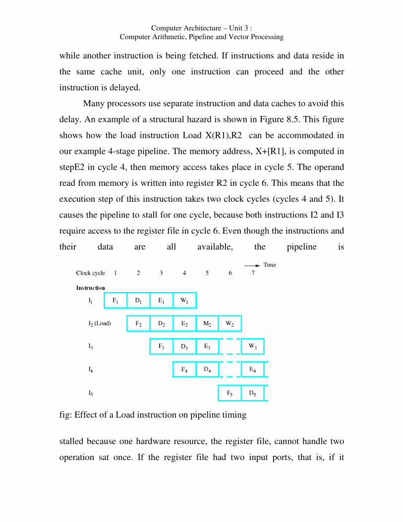
delay. An example of a structural hazard is shown in Figure 8.5. This figure
shows how the load instruction Load X(R1),R2 can be accommodated in
our example 4-stage pipeline. The memory address, X+[R1], is computed in
stepE2 in cycle 4, then memory access takes place in cycle 5. The operand
read from memory is written into register R2 in cycle 6. This means that the
execution step of this instruction takes two clock cycles (cycles 4 and 5). It
causes the pipeline to stall for one cycle, because both instructions I2 and I3
require access to the register file in cycle 6. Even though the instructions and
their data are all available, the pipeline is
fig: Effect of a Load instruction on pipeline timing
stalled because one hardware resource, the register file, cannot handle two
operation sat once. If the register file had two input ports, that is, if it

Computer Architecture – Unit 3 :
Computer Arithmetic, Pipeline and Vector Processing
allowed two simultaneous write operations, the pipeline would not be
stalled. In general, structural hazards are avoided by providing sufficient
hardware resources on the processor chip. It is important to understand that
pipelining does not result in individual instructions being executed faster;
rather, it is the throughput that increases, where throughput is measured by
the rate at which instruction execution is completed. Any time one of the
stages in the pipeline cannot complete its operation in one clock cycle, the
pipeline stalls, and some degradation in performance occurs. Thus, the
performance level of one instruction completion in each clock cycle is
actually the upper limit for the throughput achievable in a pipelined
processor organized as in Figure b. An important goal in designing
processors is to identify all hazards that may cause the pipeline to stall and
to find ways to minimize their impact. In the following sections we discuss
various hazards, starting with data hazards, followed by control hazards. In
each case we present some of the techniques used to mitigate their negative
effect on performance.
DATA HAZARDS
A data hazard is a situation in which the pipeline is stalled because the
data to be operated on are delayed for some reason. We will now examine
the issue of availability of data in some detail. Consider a program that
contains two instructions, I1 followed by I2. When this program is executed
in a pipeline, the execution of I2 can begin before the execution of I1 is
completed. This means that the results generated by I1 may not be available
for use by I2. We must ensure that the results obtained when instructions are
executed in a pipelined processor are identical to those obtained when the

Computer Architecture – Unit 3 :
Computer Arithmetic, Pipeline and Vector Processing
same instructions are executed sequentially. The potential for obtaining
incorrect results when operations are performed concurrently can be
demonstrated by a simple example. Assume that A=5, and consider the
following two operations:
A � 3 + A
B � 4 * A
When these operations are performed in the order given, the result is B = 32.
But if they are performed concurrently, the value of A used in computing B
would be the original value, 5, leading to an incorrect result. If these two
operations are performed by instructions in a program, then the instructions
must be executed one after the other, because the data used in the second
instruction depend on the result of the first instruction. On the other hand,
the two operations
A � 5 * C
B � 20 + C
can be performed concurrently, because these operations are independent.
fig: Pipeline stalled by data dependency between D2 and W1

Computer Architecture – Unit 3 :
Computer Arithmetic, Pipeline and Vector Processing
This example illustrates a basic constraint that must be enforced to guarantee
correct results. When two operations depend on each other, they must be
performed sequentially in the correct order. This rather obvious condition
has far-reaching consequences. Understanding its implications is the key to
understanding the variety of design alternatives and trade-offs encountered
in pipelined computers. Consider the pipeline Figure. The data dependency
just described arises when the destination of one instruction is used as a
source in the next instruction. For example, the two instructions
Mul R2,R3,R4
Add R5,R4,R6
give rise to a data dependency. The result of the multiply instruction is
placed into register R4, which in turn is one of the two source operands of
the Add instruction. Assuming that the multiply operation takes one clock
cycle to complete, execution would proceed as shown in Figure 8.6. As the
Decode unit decodes the Add instruction in cycle 3, it realizes that R4 is
used as a source operand. Hence, the D step of that instruction cannot be
completed until the W step of the multiply instruction has been completed.
Completion of step D2 must be delayed to clock cycle 5, and is shown as
step D2A in the figure. Instruction I3 is fetched in cycle 3, but its decoding
must be delayed because step D3 cannot precede D2. Hence, pipelined
execution is stalled for two cycles.
1. OPERAND FORWARDING
The data hazard just described arises because one instruction,
instruction I2 is waiting for data to be written in the register file. However,
these data are available at the output of the ALU once the Execute stage
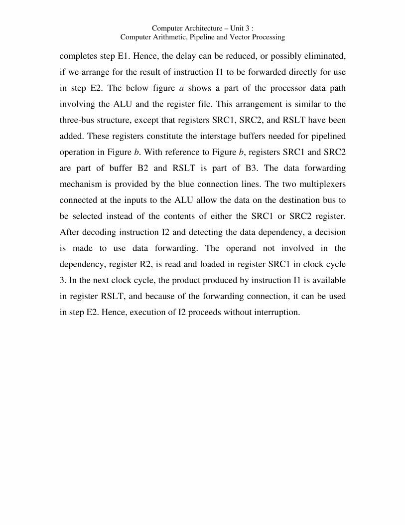
Computer Architecture – Unit 3 :
Computer Arithmetic, Pipeline and Vector Processing
completes step E1. Hence, the delay can be reduced, or possibly eliminated,
if we arrange for the result of instruction I1 to be forwarded directly for use
in step E2. The below figure a shows a part of the processor data path
involving the ALU and the register file. This arrangement is similar to the
three-bus structure, except that registers SRC1, SRC2, and RSLT have been
added. These registers constitute the interstage buffers needed for pipelined
operation in Figure b. With reference to Figure b, registers SRC1 and SRC2
are part of buffer B2 and RSLT is part of B3. The data forwarding
mechanism is provided by the blue connection lines. The two multiplexers
connected at the inputs to the ALU allow the data on the destination bus to
be selected instead of the contents of either the SRC1 or SRC2 register.
After decoding instruction I2 and detecting the data dependency, a decision
is made to use data forwarding. The operand not involved in the
dependency, register R2, is read and loaded in register SRC1 in clock cycle
3. In the next clock cycle, the product produced by instruction I1 is available
in register RSLT, and because of the forwarding connection, it can be used
in step E2. Hence, execution of I2 proceeds without interruption.

Computer Architecture – Unit 3 :
Computer Arithmetic, Pipeline and Vector Processing
fig: Operand forwarding in a pipelined processor
2. HANDLING DATA HAZARDS IN SOFTWARE
We assumed the data dependency is discovered by the hardware while
the instruction is being decoded. The control hardware delays reading
register R4 until cycle 5, thus introducing a 2-cycle stall unless operand
forwarding is used. An alternative approach is to leave the task of detecting
data dependencies and dealing with them to the software. In this case, the

Computer Architecture – Unit 3 :
Computer Arithmetic, Pipeline and Vector Processing
compiler can introduce the two-cycle delay needed between instructions I1
and I2 by inserting NOP (No-operation) instructions, as follows:
I1: Mul R2,R3,R4
NOP
NOP
I2: Add R5,R4,R6
If the responsibility for detecting such dependencies is left entirely to the
software, the compiler must insert the NOP instructions to obtain a correct
result. This possibility illustrates the close link between the compiler and the
hardware. A particular feature can be either implemented in hardware or left
to the compiler. Leaving tasks such as inserting NOP instructions to the
compiler leads to simpler hardware. Being aware of the need for a delay, the
compiler can attempt to reorder instructions to perform useful tasks in the
NOP slots, and thus achieve better performance. On the other hand, the
insertion of NOP instructions leads to larger code size. Also, it is often the
case that a given processor architecture has several hardware
implementations, offering different features. NOP instructions inserted to
satisfy the requirements of one implementation may not be needed and,
hence, would lead to reduced performance on a different implementation.
SIDE EFFECTS
The data dependencies encountered in the preceding examples are
explicit and easily detected because the register involved is named as the
destination in instruction I1 and as a source in I2. Sometimes an instruction
changes the contents of a register other than the one named as the
destination. An instruction that uses an autoincrement or autodecrement

Computer Architecture – Unit 3 :
Computer Arithmetic, Pipeline and Vector Processing
addressing mode is an example. In addition to storing new data in its
destination location, the instruction changes the contents of a source register
used to access one of its operands. All the precautions needed to handle data
dependencies involving the destination location must also be applied to the
registers affected by an autoincrement or autodecrement operation. When a
location other than one explicitly named in an instruction as a destination
operand is affected, the instruction is said to have a side effect. For example,
stack instructions, such as push and pop, produce similar side effects
because they implicitly use the autoincrement and autodecrement addressing
modes.
Another possible side effect involves the condition code flags, which are
used by instructions such as conditional branches and add-with-carry.
Suppose that registers R1 and R2 hold a double-precision integer number
that we wish to add to another doubleprecision number in registers R3 and
R4. This may be accomplished as follows:
Add R1,R3
AddWithCarry R2,R4
An implicit dependency exists between these two instructions through the
carry flag.
This flag is set by the first instruction and used in the second instruction,
which performs the operation
R4 . [R2] + [R4] + carry
Instructions that have side effects give rise to multiple data dependencies,
which lead to a substantial increase in the complexity of the hardware or
software needed to resolve them. For this reason, instructions designed for
execution on pipelined hardware should have fewside effects. Ideally, only

Computer Architecture – Unit 3 :
Computer Arithmetic, Pipeline and Vector Processing
the contents of the destination location, either a register or a memory
location, should be affected by any given instruction. Side effects, such as
setting the condition code flags or updating the contents of an address
pointer, should be kept to a minimum. However, Chapter 2 showed that the
autoincrement and autodecrement addressing modes are potentially useful.
Condition code flags are also needed for recording such information as the
generation of a carry or the occurrence of overflow in an arithmetic
operation. In Section 8.4 we show how such functions can be provided by
other means that are consistent with a pipelined organization and with the
requirements of optimizing compilers.
INSTRUCTION HAZARDS
The purpose of the instruction fetch unit is to supply the execution
units with a steady stream of instructions. Whenever this stream is
interrupted, the pipeline stalls for the case of a cache miss. A branch
instruction may also cause the pipeline to stall. We will now examine the
effect of branch instructions and the techniques that can be used for
mitigating their impact. We start with unconditional branches.
1. Unconditional branches
A sequence of instructions being executed in a two-stage pipeline.
Instructions I1 to I3 are stored at successive memory addresses, and I2 is a

Computer Architecture – Unit 3 :
Computer Arithmetic, Pipeline and Vector Processing
branch instruction. Let the branch target be instruction Ik . In clock cycle 3,
the fetch operation for instruction I3 is in progress at the same time that the
branch instruction is being decoded and the target address computed. In
clock cycle 4, the processor must discard I3, which has been incorrectly
fetched, and fetch instruction Ik . In the meantime, the hardware unit
responsible for the Execute (E) step must be told to do nothing during that
clock period. Thus, the pipeline is stalled for one clock cycle. The time lost
as a result of a branch instruction is often referred to as the branch penalty.
The branch penalty is one clock cycle. For a longer pipeline, the branch
penalty may be higher. For example, Figure 8.9a shows the effect of a
branch instruction on a four-stage pipeline. We have assumed that the
branch address is computed in step E2. Instructions I3 and I4 must be
discarded, and the target instruction, Ik , is fetched in clock cycle 5. Thus,
the branch penalty is two clock cycles. Reducing the branch penalty requires
the branch address to be computed earlier in the pipeline. Typically, the
instruction fetch unit has dedicated hardware to identify a branch instruction
and compute the branch target address as quickly as possible after an
instruction is fetched. With this additional hardware, both of these tasks can
be performed in step D2, leading to the sequence of events. In this case, the
branch penalty is only one clock cycle.

Computer Architecture – Unit 3 :
Computer Arithmetic, Pipeline and Vector Processing
fig: An idle cycle caused by a branch instruction
fig: Branch timing

Computer Architecture – Unit 3 :
Computer Arithmetic, Pipeline and Vector Processing
2. Instruction Queue and Perfecting
Either a cache miss or a branch instruction stalls the pipeline for one
or more clock cycles. To reduce the effect of these interruptions, many
processors employ sophisticated fetch units that can fetch instructions before
they are needed and put them
in a queue. Typically, the instruction queue can store several instructions. A
separate unit, which we call the dispatch unit, takes instructions from the
front of the queue and
Figure Use of an instruction queue in the hardware organization
sends them to the execution unit. The dispatch unit also performs the
decoding function.
To be effective, the fetch unit must have sufficient decoding and
processing capability to recognize and execute branch instructions. It
attempts to keep the instruction queue filled at all times to reduce the impact
of occasional delays when fetching instructions. When the pipeline stalls
because of a data hazard, for example, the dispatch unit is not able to issue
instructions from the instruction queue. However, the fetch unit continues to
fetch instructions and add them to the queue. Conversely, if there is a delay
in fetching instructions because of a branch or a cache miss, the dispatch

Computer Architecture – Unit 3 :
Computer Arithmetic, Pipeline and Vector Processing
unit continues to issue instructions from the instruction queue. how the
queue length changes and how it affects the relationship between different
pipeline stages. We have assumed that initially the queue contains one
instruction. Every fetch operation adds one instruction to the queue and
every dispatch operation reduces the queue length by one. Hence, the queue
length remains the same for the first four clock cycles. (There is both an F
and a D step in each of these cycles.) Suppose that instruction I1 introduces
a 2-cycle stall. Since space is available in the queue, the fetch unit continues
to fetch instructions and the queue length rises to 3 in clock cycle 6.
Instruction I5 is a branch instruction. Its target instruction, Ik , is fetched in
cycle 7, and instruction I6 is discarded. The branch instruction would
normally cause a stall in cycle 7 as a result of discarding instruction I6.
Instead, instruction I4 is dispatched from the queue to the decoding stage.
After discarding I6, the queue length drops to 1 in cycle 8. The queue length
will be at this value until another stall is encountered. Nowobserve the
sequence of instruction completions in Figure 8.11. Instructions I1, I2, I3, I4,
and Ik complete execution in successive clock cycles. Hence, the branch
instruction does not increase the overall execution time. This is because the
instruction fetch unit has executed the branch instruction (by computing the
branch address) concurrently with the execution of other instructions. This
technique is referred to as branch folding.

Computer Architecture – Unit 3 :
Computer Arithmetic, Pipeline and Vector Processing
Figure Branch timing in the presence of an instruction queue. Branch target
address is computed in the D stage.
Note that branch folding occurs only if at the time a branch instruction is
encountered, at least one instruction is available in the queue other than the
branch instruction. If only the branch instruction is in the queue, execution
would proceed as in Figure b. Therefore, it is desirable to arrange for the
queue to be full most of the time, to ensure an adequate supply of
instructions for processing. This can be achieved by increasing the rate at
which the fetch unit reads instructions from the cache. In many processors,
the width of the connection between the fetch unit and the instruction cache
allows reading more than one instruction in each clock cycle. If the fetch
unit replenishes the instruction queue quickly after a branch has occurred,
the probability that branch folding will occur increases. Having an
instruction queue is also beneficial in dealing with cache misses. When a
cache miss occurs, the dispatch unit continues to send instructions for

Computer Architecture – Unit 3 :
Computer Arithmetic, Pipeline and Vector Processing
execution as long as the instruction queue is not empty. Meanwhile, the
desired cache block is read
from the main memory or from a secondary cache. When fetch operations
are resumed, the instruction queue is refilled. If the queue does not become
empty, a cache miss will have no effect on the rate of instruction execution.
In summary, the instruction queue mitigates the impact of branch
instructions on performance through the process of branch folding. It has a
similar effect on stalls caused by cache misses. The effectiveness of this
technique is enhanced when the instruction fetch unit is able to read more
than one instruction at a time from the instruction cache.
3. conditional branches and branch prediction
A conditional branch instruction introduces the added hazard caused
by the dependency of the branch condition on the result of a preceding
instruction. The decision to branch cannot be made until the execution of
that instruction has been completed. Branch instructions occur frequently. In
fact, they represent about 20 percent of the dynamic instruction count of
most programs. (The dynamic count is the number of instruction executions,
taking into account the fact that some program instructions are executed
many times because of loops.) Because of the branch penalty, this large
percentage would reduce the gain in performance expected from pipelining.
Fortunately, branch instructions can be handled in several ways to reduce
their negative impact on the rate of execution of instructions.
4. Delayed Branch
The processor fetches instruction I3 before it determines whether the
current instruction, I2, is a branch instruction. When execution of I2 is
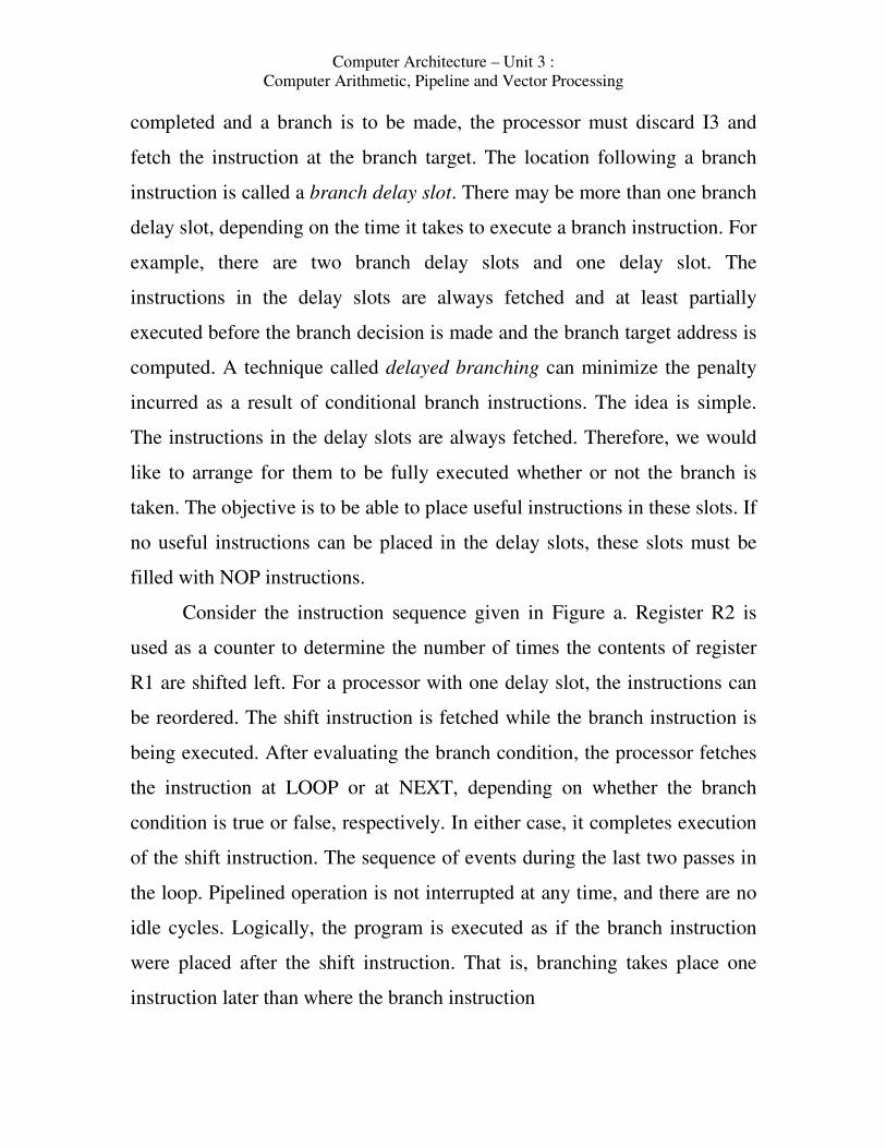
Computer Architecture – Unit 3 :
Computer Arithmetic, Pipeline and Vector Processing
completed and a branch is to be made, the processor must discard I3 and
fetch the instruction at the branch target. The location following a branch
instruction is called a branch delay slot. There may be more than one branch
delay slot, depending on the time it takes to execute a branch instruction. For
example, there are two branch delay slots and one delay slot. The
instructions in the delay slots are always fetched and at least partially
executed before the branch decision is made and the branch target address is
computed. A technique called delayed branching can minimize the penalty
incurred as a result of conditional branch instructions. The idea is simple.
The instructions in the delay slots are always fetched. Therefore, we would
like to arrange for them to be fully executed whether or not the branch is
taken. The objective is to be able to place useful instructions in these slots. If
no useful instructions can be placed in the delay slots, these slots must be
filled with NOP instructions.
Consider the instruction sequence given in Figure a. Register R2 is
used as a counter to determine the number of times the contents of register
R1 are shifted left. For a processor with one delay slot, the instructions can
be reordered. The shift instruction is fetched while the branch instruction is
being executed. After evaluating the branch condition, the processor fetches
the instruction at LOOP or at NEXT, depending on whether the branch
condition is true or false, respectively. In either case, it completes execution
of the shift instruction. The sequence of events during the last two passes in
the loop. Pipelined operation is not interrupted at any time, and there are no
idle cycles. Logically, the program is executed as if the branch instruction
were placed after the shift instruction. That is, branching takes place one
instruction later than where the branch instruction

Computer Architecture – Unit 3 :
Computer Arithmetic, Pipeline and Vector Processing
appears in the instruction sequence in the memory, hence the name “delayed
branch.”
Figure Reordering of instructions for a delayed branch
Figure : Execution timing showing the delay slot being filled during the last
two passes through the loop.

Computer Architecture – Unit 3 :
Computer Arithmetic, Pipeline and Vector Processing
The effectiveness of the delayed branch approach depends on how
often it is possible to reorder instructions. Experimental data collected from
many programs indicate that sophisticated compilation techniques can use
one branch delay slot in as many as 85 percent of the cases. For a processor
with two branch delay slots, the compiler attempts to find two instructions
preceding the branch instruction that it can move into the delay slots without
introducing a logical error. The chances of finding two such instructions are
considerably less than the chances of finding one. Thus, if increasing the
number of pipeline stages involves an increase in the number of branch
delay slots, the potential gain in performance may not be fully realized.
5. Branch Prediction
Another technique for reducing the branch penalty associated with
conditional branches is to attempt to predict whether or not a particular
branch will be taken. The simplest form of branch prediction is to assume
that the branch will not take place and to
continue to fetch instructions in sequential address order. Until the branch
condition is evaluated, instruction execution along the predicted path must
be done on a speculative basis. Speculative execution means that instructions
are executed before the processor is certain that they are in the correct
execution sequence. Hence, care must be taken that no processor registers or
memory locations are updated until it is confirmed that these instructions
should indeed be executed. If the branch decision indicates otherwise, the
instructions and all their associated data in the execution units must be
purged, and the correct instructions fetched and executed. An incorrectly
predicted branch is illustrated in Figure for a four-stage pipeline.

Computer Architecture – Unit 3 :
Computer Arithmetic, Pipeline and Vector Processing
The figure shows a Compare instruction followed by a Branch>0
instruction. Branch prediction takes place in cycle 3, while instruction I3 is
being fetched.
Figure Timing when a branch decision has been incorrectly
predicted as not taken.
The fetch unit predicts that the branch will not be taken, and it continues to
fetch instruction I4 as I3 enters the Decode stage. The results of the compare
operation are available at the end of cycle 3. Assuming that they are
forwarded immediately to the instruction fetch unit, the branch condition is
evaluated in cycle 4. At this point, the instruction fetch unit realizes that the
prediction was incorrect, and the two instructions in the execution pipe are
purged. A new instruction, Ik , is fetched from the branch target address in
clock cycle 5. If branch outcomes were random, then half the branches
would be taken. Then the simple approach of assuming that branches will
not be taken would save the time lost to conditional branches 50 percent of
the time. However, better performance can be achieved if we arrange for
some branch instructions to be predicted as taken and others as not taken,
depending on the expected program behavior. For example, a branch
instruction at the end of a loop causes a branch to the start of the loop for

Computer Architecture – Unit 3 :
Computer Arithmetic, Pipeline and Vector Processing
every pass through the loop except the last one. Hence, it is advantageous to
assume that this branch will be taken and to have the instruction fetch unit
start to fetch instructions at the branch target address. On the other hand, for
a branch instruction at the beginning of a program loop, it is advantageous to
assume that the branch will not be taken. A decision on which way to predict
the result of the branch may be made in hardware by observing whether the
target address of the branch is lower than or higher than the address of the
branch instruction. A more flexible approach is to have the compiler decide
whether a given branch instruction should be predicted taken or not taken.
The branch instructions of some processors, such as SPARC, include a
branch prediction bit, which is set to 0 or 1 by the compiler to indicate the
desired behavior. The instruction fetch unit checks this bit to predict whether
the branch will be taken or not taken. With either of these schemes, the
branch prediction decision is always the same every time a given instruction
is executed. Any approach that has this characteristic is called static branch
prediction. Another approach in which the prediction decision may change
depending on execution history is called dynamic branch prediction.
6. Dynamic Branch Prediction
The objective of branch prediction algorithms is to reduce the
probability of making a wrong decision, to avoid fetching instructions that
eventually have to be discarded. In dynamic branch prediction schemes, the
processor hardware assesses the likelihood of a given branch being taken by
keeping track of branch decisions every time that instruction is executed. In
its simplest form, the execution history used in predicting the outcome of a
given branch instruction is the result of the most recent execution of that

Computer Architecture – Unit 3 :
Computer Arithmetic, Pipeline and Vector Processing
instruction. The processor assumes that the next time the instruction is
executed, the result is likely to be the same. Hence, the algorithm may be
described by the two-state machine in
The two states are:
• LT: Branch is likely to be taken
• LNT: Branch is likely not to be taken
Figure State-machine representation of branch-prediction algorithms.
Suppose that the algorithm is started in state LNT. When the branch
instruction is executed and if the branch is taken, the machine moves to state
LT. Otherwise, it remains in state LNT. The next time the same instruction
is encountered, the branch is predicted as taken if the corresponding state
machine is in state LT. Otherwise it is predicted as not taken. This simple
scheme, which requires one bit of history information for each branch
instruction, works well inside program loops. Once a loop is entered, the
branch instruction that controls looping will always yield the same result

Computer Architecture – Unit 3 :
Computer Arithmetic, Pipeline and Vector Processing
until the last pass through the loop is reached. In the last pass, the branch
prediction will turn out to be incorrect, and the branch history state machine
will be changed to the opposite state. Unfortunately, this means that the next
time this same loop is entered, and assuming that there will be more than one
pass through the loop, the machine will lead to the wrong prediction.
Better performance can be achieved by keeping more information about
execution history. An algorithm that uses 4 states, thus requiring two bits of
history information for each branch instruction.
The four states are:
• ST: Strongly likely to be taken
• LT: Likely to be taken
• LNT: Likely not to be taken
• SNT: Strongly likely not to be taken
Again assume that the state of the algorithm is initially set to LNT. After the
branch instruction has been executed, and if the branch is actually taken, the
state is changed to ST; otherwise, it is changed to SNT. As program
execution progresses and the same instruction are encountered again, the
state of the branch prediction algorithm continues to change as shown. When
a branch instruction is encountered, the instruction fetch unit predicts that
the branch will be taken if the state is either LT or ST, and it begins to fetch
instructions at the branch target address. Otherwise, it continues to fetch
instructions in sequential address order.
It is instructive to examine the behavior of the branch prediction algorithm
in some detail. When in state SNT, the instruction fetch unit predicts that the
branch will not be taken. If the branch is actually taken, that is if the
prediction is incorrect, the state changes to LNT. This means that the next

Computer Architecture – Unit 3 :
Computer Arithmetic, Pipeline and Vector Processing
time the same branch instruction is encountered; the instruction fetch unit
will still predict that the branch will not be taken. Only if the prediction is
incorrect twice in a row will the state change to ST. After that, the branch
will be predicted as taken. Let us reconsider what happens when executing a
program loop. Assume that the branch instruction is at the end of the loop
and that the processor sets the initial state of the algorithm to LNT. During
the first pass, the prediction will be wrong (not taken), and hence the state
will be changed to ST. In all subsequent passes the prediction will be
correct, except for the last pass. At that time, the state will change to LT.
When the loop is entered a second time, the prediction will be correct
(branch taken).
We now add one final modification to correct the mispredicted branch at the
time the loop is first entered. The cause of the misprediction in this case is
the initial state of the branch prediction algorithm. In the absence of
additional information about the nature of the branch instruction, we
assumed that the processor sets the initial state to LNT. The information
needed to set the initial state correctly can be provided by any of the static
prediction schemes discussed earlier. Either by comparing addresses or by
checking a prediction bit in the instruction, the processor sets the initial state
of the algorithm to LNT or LT. In the case of a branch at the end of a loop,
the compiler would indicate that the branch should be predicted as taken,
causing the initial state to be set to LT. With this modification, branch
prediction will be correct all the time, except for the final pass through the
loop. Misprediction in this latter case is unavoidable. The state information
used in dynamic branch prediction algorithms may be kept by the processor
in a variety of ways. It may be recorded in a look-up table, which is accessed

Computer Architecture – Unit 3 :
Computer Arithmetic, Pipeline and Vector Processing
using the low-order part of the branch instruction address. In this case, it is
possible for two branch instructions to share the same table entry. This may
lead to a branch being mispredicted, but it does not cause an error in
execution. Misprediction only introduces a small delay in execution time.
An alternative approach is to store the history bits as a tag associated with
branch instructions in the instruction cache.
INFLUENCE ON INSTRUCTION SETS
We have seen that some instructions are much better suited to
pipelined execution than others. For example, instruction side effects can
lead to undesirable data dependencies. In this section, we examine the
relationship between pipelined execution and machine instruction features.
We discuss two key aspects of machine instructions—addressing modes and
condition code flags.
1. ADDRESSING MODES
Addressing modes should provide the means for accessing a variety of
data structures simply and efficiently. Useful addressing modes include
index, indirect, autoincrement, and autodecrement. Many processors provide
various combinations of these modes to increase the flexibility of their
instruction sets. Complex addressing modes, such as those involving double
indexing, are often encountered. In choosing the addressing modes to be
implemented in a pipelined processor, we must consider the effect of each
addressing mode on instruction flow in the pipeline. Two important
considerations in this regard are the side effects of modes such as
autoincrement and autodecrement and the extent to which complex

Computer Architecture – Unit 3 :
Computer Arithmetic, Pipeline and Vector Processing
addressing modes cause the pipeline to stall. Another important factor is
whether a given mode is likely to be used by compilers.
To compare various approaches, we assume a simple model for accessing
operands in the memory. The load instruction Load X(R1),R2 takes five
cycles to complete execution. However, the instruction
Load (R1),R2
can be organized to fit a four-stage pipeline because no address computation
is required.
Access to memory can take place in stage E. A more complex addressing
mode may require several accesses to the memory to reach the named
operand. For example, the instruction
Load (X(R1)),R2
may be executed and assuming that the index offset, X, is given in the
instruction word. After computing the address in cycle 3, the processor
needs to access memory twice — first to read location X+[R1] in clock
cycle 4 and then to read location [X+[R1]] in cycle 5. If R2 is a source
operand in the next instruction, that instruction would be stalled for three
cycles, which can be reduced to two cycles with operand forwarding, as
shown.

Computer Architecture – Unit 3 :
Computer Arithmetic, Pipeline and Vector Processing
Figure : Equivalent operations using complex and simple addressing
modes.
To implement the same Load operation using only simple addressing modes
requires several instructions. For example, on a computer that allows three
operand addresses, we can use
Add #X,R1,R2
Load (R2),R2
Load (R2),R2
The Add instruction performs the operation R2.X+[R1]. The two Load
instructions fetch the address and then the operand from the memory. This
sequence of instructions takes exactly the same number of clock cycles as
the original, single Load instruction.
This example indicates that, in a pipelined processor, complex addressing
modes that involve several accesses to the memory do not necessarily lead to
faster execution. The main advantage of such modes is that they reduce the
Computer Architecture – Unit 3 :
Computer Arithmetic, Pipeline and Vector Processing
number of instructions needed to perform a given task and thereby reduce
the program space needed in the main memory. Their main disadvantage is
that their long execution times cause the pipeline to stall, thus reducing its
effectiveness. They require more complex hardware to decode and execute
them. Also, they are not convenient for compilers to work with. The
instruction sets of modern processors are designed to take maximum
advantage of pipelined hardware. Because complex addressing modes are
not suitable for pipelined execution, they should be avoided. The addressing
modes used in modern processors often have the following features:
• Access to an operand does not require more than one access to the
memory.
• Only load and store instructions access memory operands.
• The addressing modes used do not have side effects.
Three basic addressing modes that have these features are register, register
indirect, and index. The first two require no address computation. In the
index mode, the address can be computed in one cycle, whether the index
value is given in the instruction or in a register. Memory is accessed in the
following cycle. None of these modes has any side effects, with one possible
exception. Some architecture, such as ARM, allows the address computed in
the index mode to be written back into the index register. This is a side
effect that would not be allowed under the guidelines above. Note also that
relative addressing can be used; this is a special case of indexed addressing
in which the program counter is used as the index register. The three features
just listed were first emphasized as part of the concept of RISC processors.
2. CONDITION CODES

Computer Architecture – Unit 3 :
Computer Arithmetic, Pipeline and Vector Processing
In many processors, the condition code flags are stored in the
processor status register. They are either set or cleared by many instructions,
so that they can be tested by subsequent conditional branch instructions to
change the flow of program execution. An optimizing compiler for a
pipelined processor attempts to reorder instructions to avoid stalling the
pipeline when branches or data dependencies between successive
instructions occur. In doing so, the compiler must ensure that reordering
does not cause a change in the outcome of a computation. The dependency
introduced by the condition-code flags reduces the flexibility available for
the compiler to reorder instructions. Consider the sequence of instructions,
and assume that the execution of the Compare and Branch=0 instructions
proceeds. The branch decision takes place in step E2 rather than D2 because
it must await the result of the Compare instruction. The execution time of
the Branch instruction can be reduced
Figure Instruction reordering
by interchanging the Add and Compare instructions. This will delay the
branch instruction by one cycle relative to the Compare instruction. As a
result, at the time the Branch instruction is being decoded the result of the
Compare instruction will be available and a correct branch decision will be

Computer Architecture – Unit 3 :
Computer Arithmetic, Pipeline and Vector Processing
made. There would be no need for branch prediction. However,
interchanging the Add and Compare instructions can be done only if the Add
instruction does not affect the condition codes. These observations lead to
two important conclusions about the way condition codes should be handled.
First, to provide flexibility in reordering instructions, the condition-code
flags should be affected by as few instructions as possible. Second, the
compiler should be able to specify in which instructions of a program the
condition codes are affected and in which they are not. An instruction set
designed with pipelining in mind usually provides the desired flexibility.
The instructions reordered assuming that the condition code flags are
affected only when this is explicitly stated as part of the instruction OP code.
The SPARC and ARM architectures provide this flexibility.
DATAPATH AND CONTROL CONSIDERATIONS
Organization of the internal data path of a processor and the three-bus
structures are presented here. To make it suitable for pipelined execution, it
can be modified and it is shown in the Figure(to support a 4-stage
pipeline).The resources involved in stages F and E are shown in blue and
those used in stages D and W in black. Operations in the data cache may
happen during stage E or at a later stage, depending on the addressing mode

Computer Architecture – Unit 3 :
Computer Arithmetic, Pipeline and Vector Processing
and the implementation details.
Figure Data path modified for pipelined execution with interstage buffers at
the input and output of the ALU.
Several changes to be noted:
1. There are separate instruction and data caches that use separate address
and data
connections to the processor. This requires two versions of the MAR
register, IMAR for accessing the instruction cache and DMAR for accessing
the data cache.
2. The PC is connected directly to the IMAR, so that the contents of the PC
can be transferred to IMAR at the same time that an independent ALU
operation is taking place.

Computer Architecture – Unit 3 :
Computer Arithmetic, Pipeline and Vector Processing
3. The data address in DMAR can be obtained directly from the register file
or from the ALU to support the register indirect and indexed addressing
modes.
4. Separate MDR registers are provided for read and write operations. Data
can be transferred directly between these registers and the register file during
load and store
operations without the need to pass through the ALU.
5. Buffer registers have been introduced at the inputs and output of the ALU.
These are registers SRC1, SRC2, and RSLT in Figure 8.7. Forwarding
connections are not included in Figure 8.18. They may be added if desired.
6. The instruction register has been replaced with an instruction queue,
which is loaded from the instruction cache.
7. The output of the instruction decoder is connected to the control signal
pipeline. The need for buffering control signals and passing them from one
stage to the next along with the instruction is discussed in Section 8.1. This
pipeline holds the control signals in buffers B2 and B3 in Figure 8.2a.
The following operations can be performed independently in the processor
� Reading an instruction from the instruction cache
� Incrementing the PC
� Decoding an instruction
� Reading from or writing into the data cache
� Reading the contents of up to two registers from the register file
� Writing into one register in the register file
� Performing an ALU operation
Because these operations do not use any shared resources, they can be
performed

Computer Architecture – Unit 3 :
Computer Arithmetic, Pipeline and Vector Processing
simultaneously in any combination. The structure provides the flexibility
required to
implement the four-stage pipeline. For example, let I1, I2, I3, and I4 be a
sequence of four instructions.
The following actions all happen during clock cycle 4:
� Write the result of instruction I1 into the register file
� Read the operands of instruction I2 from the register file
� Decode instruction I3
� Fetch instruction I4 and increment the PC.
PERFORMANCE CONSIDERATIONS
The execution time, T , of a program that has a dynamic instruction count N
is given by
R
SNT
*=
where S is the average number of clock cycles it takes to fetch and execute
one instruction, and R is the clock rate. This simple model assumes that
instructions are executed one after the other, with no overlap. A useful
performance indicator is the instruction throughput, which is the number of
instructions executed per second. For sequential execution, the throughput,
Ps is given by
S
RPs =
In this section, we examine the extent to which pipelining increases
instruction throughput. The only real measure of performance is the total

Computer Architecture – Unit 3 :
Computer Arithmetic, Pipeline and Vector Processing
execution time of a program. Higher instruction throughput will not
necessarily lead to higher performance if a larger number of instructions is
needed to implement the desired task. For this reason, the SPEC ratings
provide a much better indicator when comparing two processors. A four-
stage pipeline structure may increase instruction throughput by a factor of
four. In general, an n-stage pipeline has the potential to increase throughput
n times. Thus, it would appear that the higher the value of n, the larger the
performance gains.
This leads to two questions:
� How much of this potential increase in instruction throughput can be
realized in practice?
� What is a good value for n?
Any time a pipeline is stalled, the instruction throughput is reduced. Hence,
the performance of a pipeline is highly influenced by factors such as branch
and cache miss penalties. First, we discuss the effect of these factors on
performance, and then we return to the question of how many pipeline stages
should be used.
1. Effect of instruction hazards
The effects of various hazards have been examined qualitatively in the
previous sections. We now assess the impact of cache misses and branch
penalties in quantitative terms. Consider a processor that uses the four-stage
pipeline. The clock rate, hence the time allocated to each step in the pipeline,
is determined by the longest step. Let the delay through the ALU be the
critical parameter. This is the time needed to add two integers. Thus, if the
ALU delay is 2 ns, a clock of 500 MHz can be used. The on-chip instruction

Computer Architecture – Unit 3 :
Computer Arithmetic, Pipeline and Vector Processing
and data caches for this processor should also be designed to have an access
time of 2 ns. Under ideal conditions, this pipelined processor will have an
instruction throughput, Pp, given by
PP = R = 500 MIPS (million instructions per second)
To evaluate the effect of cache misses. The cache miss penalty, Mp, in that
system is computed to be 17 clock cycles. Let TI be the time between two
successive instruction completions. For sequential execution, TI = S.
However, in the absence of hazards, a pipelined processor completes the
execution of one instruction each clock cycle, thus, TI = 1 cycle. A cache
miss stalls the pipeline by an amount equal to the cache miss penalty. This
means that the value of TI increases by an amount equal to the cache miss
penalty for the instruction in which the miss occurs. A cache miss can occur
for either instructions or data. Consider a computer that has a shared cache
for both instructions and data, and let d be the percentage of instructions that
refer to data operands in the memory. The average increase in the value of TI
as a result of cache misses is given by
δmiss = ((1 - hi ) + d(1 - hd )) x Mp
where hi and hd are the hit ratios for instructions and data, respectively.
Assume that 30 percent of the instructions access data in memory. With a
95-percent instruction hit rate and a 90-percent data hit rate, δmiss is given by
δmiss = (0.05 + 0.3 x 0.1) x 17 = 1.36 cycles
Taking this delay into account, the processor’s throughput would be
RR
T
RP
missI
P 42.01
=+
==δ
Note that with R expressed in MHz, the throughput is obtained directly in
millions of instructions per second. For R = 500 MHz, Pp = 210 MIPS.

Computer Architecture – Unit 3 :
Computer Arithmetic, Pipeline and Vector Processing
Let us compare this value to the throughput obtainable without pipelining. A
processor that uses sequential execution requires four cycles per instruction.
Its throughput would be RR
Pmiss
S 19.04
=+
=δ
For R = 500 MHz, Ps = 95 MIPS. Clearly, pipelining leads to significantly
higher throughput. But the performance gain of 0.42/0.19 = 2.2 is only
slightly better than one-half the ideal case. Reducing the cache miss penalty
is particularly worthwhile in a pipelined processor.
This can be achieved by introducing a secondary cache between the primary,
on-chip cache and the memory. Assume that the time needed to transfer an
8-word block from the secondary cache is 10 ns. Hence, a miss in the
primary cache for which the required block is found in the secondary cache
introduces a penalty, Ms , of 5 cycles. In the case of a miss in the secondary
cache, the full 17-cycle penalty (Mp) is still incurred. Hence, assuming a hit
rate hs of 94 percent in the secondary cache, the average increase in TI is
δmiss = ((1 - hi ) + d(1 - hd )) x (hs x Ms + (1 - hs) x Mp) = 0.46 cycle.
The instruction throughput in this case is 0.68R, or 340 MIPS. An equivalent
nonpipelined processor would have a throughput of 0.22R, or 110 MIPS.
Thus, pipelining provides a performance gain of 0.68/0.22 = 3.1.
The values of 1.36 and 0.46 are, in fact, somewhat pessimistic, because we
have assumed that every time a data miss occurs, the entire miss penalty is
incurred. This is the case only if the instruction immediately following the
instruction that references memory is delayed while the processor waits for
the memory access to be completed. However, an optimizing compiler
attempts to increase the distance between two instructions that create a
dependency by placing other instructions between them whenever possible.

Computer Architecture – Unit 3 :
Computer Arithmetic, Pipeline and Vector Processing
Also, in a processor that uses an instruction queue, the cache miss penalty
during instruction fetches may have a much reduced effect as the processor
is able to dispatch instructions from the queue.
Number of pipeline stages
The fact that an n-stage pipeline may increase instruction throughput
by a factor of n suggests that we should use a large number of stages.
However, as the number of pipeline stages increases, so does the probability
of the pipeline being stalled, because more instructions are being executed
concurrently. Thus, dependencies between instructions that are far apart may
still cause the pipeline to stall. Also, branch penalties may become more
significant. For these reasons, the gain from increasing the value of n begins
to diminish, and the associated cost is not justified. Another important factor
is the inherent delay in the basic operations performed by the processor. The
most important among these is the ALU delay. In many processors, the cycle
time of the processor clock is chosen such that one ALU operation can be
completed in one cycle. Other operations are divided into steps that take
about the same time as an add operation. It is also possible to use a pipelined
ALU. For example, the ALU of the Compaq Alpha 21064 processor consists
of a two-stage pipeline, in which each stage completes its operation in 5 ns.
Many pipelined processors use four to six stages. Others divide instruction
execution into smaller steps and use more pipeline stages and a faster clock.
For example, the UltraSPARC II uses a 9-stage pipeline and Intel’s Pentium
Pro uses a 12-stage pipeline. The latest Intel processor, Pentium 4, has a 20-
stage pipeline and uses a clock speed in the range 1.3 to 1.5 GHz. For fast
operations, there are two pipeline stages in one clock cycle.

Computer Architecture – Unit 3 :
Computer Arithmetic, Pipeline and Vector Processing
EXCEPTION HANDLING
A method for processing address translation exceptions occurring in a
virtual memory system employing demand paging and having a plurality of
registers and a real storage area, includes the steps of:
(a) temporarily storing for each storage operation;
(i) the effective storage address for the operation;
(ii) exception control word information relative to the ones of
the registers
involved in the operation and the length and type of the
operation; and
(iii) any data to be stored during the operation;
(b) retrieving the temporarily stored information to form an exception
status block
if an exception is generated indicating a failed operation; and
(c) reinitiating the failed operation based on the information
contained in the
exception status block.
Unit Summary

Computer Architecture – Unit 3 :
Computer Arithmetic, Pipeline and Vector Processing
Two important features have been introduced in this chapter, pipelining and
multiple issue. Pipelining enables us to build processors with instruction
throughput approaching one instruction per clock cycle. Multiple issue
makes possible superscalar operation, with instruction throughput of several
instructions per clock cycle. The potential gain in performance can only be
realized by careful attention to three aspects:
• The instruction set of the processor
• The design of the pipeline hardware
• The design of the associated compiler
It is important to appreciate that there are strong interactions among all
three. High performance is critically dependent on the extent to which these
interactions are taken into account in the design of a processor. Instruction
sets that are particularly well-suited for pipelined execution are key features
of modern processors.
Key terms
Pipelining
Data hazard
Structural Hazard
Control hazards or instruction hazards
Fetching instructions
Executing instructions
Operand Forwarding
Objective type questions
1.Assume a processor takes 3 cycles to execute any instruction (fetch,
decode, execute) How many cycles would a non-pipelined processor take to
execute 6 instructions?
a) 12 cycles
b) 18 cycles

Computer Architecture – Unit 3 :
Computer Arithmetic, Pipeline and Vector Processing
c) 3 cycles
d) 6 cycles
2. Assume a processor takes 3 cycles to execute any instruction (fetch,
decode, execute) How many cycles would a pipelined processor take to
execute 6 instructions?
a) 12 cycles
b) 18 cycles
c) 3 cycles
d) 8 cycles
3. Pipeline implement
a. fetch instruction
b. decode instruction
c. fetch operand
d. calculate operand
e. execute instruction
f. all of the above
4. Where does a computer add and compare data?
a. Hard disk
b. Floppy disk
c. CPU chip
d. Memory chip
5. Pipelining strategy is called implement
a. instruction execution
b. instruction prefetch
c. instruction decoding
d. instruction manipulation
Part A Questions
1. What is pipelining?
A pipeline may be visualized as a collection of segments called pipe stages
through which binary information flows. Each segment performs partial

Computer Architecture – Unit 3 :
Computer Arithmetic, Pipeline and Vector Processing
processing as dictated by the task. The result obtained in each segment is
transferred to the next segment in the pipeline. The final result is
obtained after the data passes through all the segments.
2. Explain Latency and Throughput.
Latency: Each instruction takes certain amount of time to complete. This
is called as latency. It is the time difference between when an instruction
is issued and when it is completed. Throughput: The number of
instructions completed in a given time is called throughput.
3. What axe the major characteristics of a pipeline?
1. Pipelining cannot be implemented on a single task, as it works by
splitting multiple tasks into a
number of subtasks and operating on them simultaneously.
2. The speedup or efficiency is achieved by using a pipeline depends on
the number of pipe stages
and the number of available tasks that can be subdivided.
3. If the split-able task has uneven length of execution times, then the
speedup of the pipeline is
reduced.
4. Though the pipelining architecture does not reduce the time of
execution of a single task, it reduces
the overall time taken for the entire job to get completed.
4. What are the main issues in designing pipelined computers?
1. Job sequencing and congestion control
2. Collision prevention, branch handling and reconfiguration
3. Hazard resolution are the main issues in the design of a pipelined

Computer Architecture – Unit 3 :
Computer Arithmetic, Pipeline and Vector Processing
computer
5. What is precise exception?
A precise exception is one in which all instructions prior to the faulting
instruction are complete and instruction following the faulting
instruction, including the faulting instruction, do not change the state of
the machine.
6. What is imprecise exception?
A imprecise exception is one in which all instructions prior to the
faulting instruction are not complete and instruction following the
faulting instruction, including the faulting instruction, change the state
of the machine
7. Define Job sequencing.
Job sequencing is the process of scheduling tasks that are awaiting
initiation in order to avoid collisions and achieve high throughput.
8. Define Collision.
Once a task is initiated in a pipeline, it follows a fixed pattern of flow.
The start of a single function evaluation is called an initiation. When
two or more such initiations start using the same stage of a pipeline at
the same time, collision is said to occur.
9. Define Speedup of a pipeline.
Speedup is the ratio of the average instruction time without pipelining to
the average instruction time with pipelining.

Computer Architecture – Unit 3 :
Computer Arithmetic, Pipeline and Vector Processing
Average instruction time without pipelining
Speedup = ___________________________________
Average instruction time with pipelining
10. What is pipeline register delay?
Adding registers between pipeline stages means adding logic between
stages and setup and hold times for proper operations. This delay is
known as pipeline register delay.
11. Define Pipeline hazards.
The pipeline architecture works smoothly as long as it is able to take up
a new task in every machine cycle. In practice there are situations when
the next instruction cannot be executed in the following machine cycle.
These events are called as Pipeline hazards.
12. What arc the types of Pipeline hazards?
1. Structural Hazard
2. Data Hazard
3. Control Hazard
13. Define Structural hazard.
The structural hazard happens when there are conflicts over the same
hardware resource by two different pipeline cycles.
14. Define Data hazard.
Data hazard occurs when an instruction is waiting for data that is not yet
available because the previous instruction has not completed or stored.
15. Define Control Hazard.

Computer Architecture – Unit 3 :
Computer Arithmetic, Pipeline and Vector Processing
Control hazard occurs normally due to branch instructions since the
branch condition (for compare and branch) and the branch address are not
available in rime to fetch the next instruction on the next clock cycle.
16. What is pipeline stall?
In the case of all hazard, two simultaneous actions tend to take place in the
same machine cycle causing hazard. This can be avoided by letting the
computer go through an empty cycle without doing any useful work and
postponing one of the actions to the next cycle. This kind of empty cycle
is called a stall. A pipeline stall is also called a pipeline bubble or simply
bubble.
17. List any two conditions when a processor can stall?
1. Cache miss
2. Hazard in pipeline
18. List the types of data hazards.
1. RAW (Read After -Write)
2. WAW (Write After Write)
3. WAR (Write After Read)
4. RAR (Read After Read)
19. List the techniques used for overcoming hazards?
1. Data forwarding
2. Adding sufficient hardware
3. Stalling instructions
4. Document to find instruction in wrong order
20. What are the techniques used to prevent Control hazards?
1. Scheduling instructions in delay slots

Computer Architecture – Unit 3 :
Computer Arithmetic, Pipeline and Vector Processing
2. Loop unrolling
3. Conditional execution
4. Speculation (by both compiler and CPU)
21. What is instruction level parallelism?
Pipelining increases performance by overlapping execution of
independent instructions. The potential to overlap instructions is called
Instruction-Level Parallelism (ILP) since the instructions are evaluated in
parallel.
22. Define basic block.
The basic block is a block of code with no branches into the code except
at the start and no branches out of the code except at the end. That is, the
set of instructions between entry points and between branches. A basic
block has only one entry and exit.
23. Define Loop Level Parallelism.
Parallelism among iterations in a loop is called as Loop Level Parallelism
(LLP).
24. What is dependence?
Dependences are the property of programs, not of CPUs or pipelines.
Dependence between two instructions will always exist unless the
program is changed.
25. What are the types of dependences?

Computer Architecture – Unit 3 :
Computer Arithmetic, Pipeline and Vector Processing
1. Data dependence
2. Name dependence
3. Control dependence
26. List some characteristics of Data dependences.
1. Indicate the possibility of hazard
2. Determine the order in which results must be generated
3. Place an upper bound on the amount of ILP that is available
27. How to overcome the Data dependences.
There are two ways to overcome the Data dependences r
1. Maintaining the dependence but avoiding the hazard.
2. Eliminating the dependence by transforming the code.
28. What is Name dependence?
Name dependence is said to occur when two instructions use the same
register or memory location and there is no flow of data between
instructions that use the same name.
29. What are the types of Name dependences?
1. And dependence
2. Output dependence
30. What is meant by anti dependence?

Computer Architecture – Unit 3 :
Computer Arithmetic, Pipeline and Vector Processing
Assume instruction '1' precedes instruction 'j '. Anti dependence occurs if
'j' writes to a register or memory location while 'i1 reads and is executed
first. This corresponds to WAR hazard.
31. What is meant by Control dependence?
Assume instruction 'i' precedes instruction 'j'. Control dependence
occurs when 'i' and 'j' write to the same register or memory location,
resulting in a WAW hazard and instruction order is to be maintained.
32. Define Dynamic scheduling.
The CPU rearranges the instruction to reduce stalls while preserving
dependences and this technique is called as dynamic scheduling. It uses a
hardware based mechanism to rearrange instruction execution order to
reduce stalls at run-time and enables handling cases where dependences
are unknown at compile time.
33. What is Score boarding?
Score boarding is a hardware mechanism that maintains an execution rate
of one instruction per cycle by executing an instruction as soon as its
operands are made available and no hazard condition prevent it.
34. List the pipeline stages of a Scoreboard control.
1. Issue (ID1)
2. Read operands (ID2)
3. Execution (EX)
4. Write result (WB)
35. List the parts of Scoreboard?
1. Instruction status
2. Functional unit status

Computer Architecture – Unit 3 :
Computer Arithmetic, Pipeline and Vector Processing
3. 'busy' indicates whether particular unit is busy
4. 'op' indicates operation to be performed in the functional unit
5. 'Fi, Fj, Fk' indicates the source and destination registers of
instruction
6. Rj, Rk are flags indicating when Fj, Fk are ready
7. Register result status
36. Write short notes on Tomasulo's Approach?
This technique allows execution of instruction to proceed in the presence
of hazards. This can only be applied to floating point operations.
Tomasulo's scheme allows renaming of registers dynamically. It buffers
operands of instructions waiting to issue, fetch them as soon as they are
available.
37. What are the differences between Scoreboarding and Tomasulo's
Approach?
S.No. Scoreboarding Tomasulo's Approach
1 Score boarding must wait
for WAR and WAW
hazards to clear
Register renaming is used to
eliminate WAR and WAW
hazards 2 Hazard detection and
execution control is
centralized
Hazard detection and execution
control is distributed to each
functional unit 3 Result is forwarded to the
register file
Forwards results directly to the
functional units
38. What is BTB?
A BTB (Branch Target Buffer) is an associative memory where the
addresses of branch instructions are stored along with their target
addresses.

Computer Architecture – Unit 3 :
Computer Arithmetic, Pipeline and Vector Processing
39. Define dynamic scheduling.
The CPU rearranges the instruction to reduce stalls while preserving
dependences and this technique is called as dynamic scheduling. It uses a
hardware based mechanism to rearrange instruction execution order to
reduce stalls at run-time and enables handling cases where dependences
are unknown at compile time.
40. WhatisBTIC?
In BTIC (Branch Target Instruction Cache), code of the branch target
instruction is cached in addition to its address. This eliminates the need to
fetch the target instruction from the instruction
cache or memory.
41. What are the effects of branch prediction on performance?
Accuracy The accuracy of the branch prediction scheme impacts CPU
performance. A scheme that is not accurate may make CPU performance
worse than it would otherwise be.
Latency There are 4 different latencies for a single branch condition,
1. Branch may be taken predicted correctly
2. Branch may be taken predicted incorrectly
3. Branch may not be taken predicted correctly
4. Branch may not be taken predicted incorrectly
42. What are the limitations of branch prediction?
Misprediction rate and Misprcdiction penalties.

Computer Architecture – Unit 3 :
Computer Arithmetic, Pipeline and Vector Processing
43. What are the drawbacks of pipelined computers?
Modern pipelined computers achieve high performance by breaking up the
execution of an instruction into separate operations and concurrently
executing those operations in parallel. This can lower the cycle time and
allow one instruction to complete in every clock cycle. They issue only one
instruction in one clock cycle and this places an upper limit on performance
of these computers to keep the CPI closer to 1.
44. Define Operational latency.
It is the time in cycles between the issue of instruction and the result, which
is available for use by subsequent instruction.
45. What is issue latency?
It is the time in cycles required between issuing two instructions.
46. What is instruction class?
A group of instructions that are issued to the same type of functional unit.
PART-B
1. Design a 4-stage instruction pipeline and show how its performance is
improved over sequential execution.
2. Explain the function of a six segment pipelines and draw a space
diagram for a six segment pipeline showing the time it takes to
process eight tasks.
3. Explain the performance of the instruction pipeline can be improved.

Computer Architecture – Unit 3 :
Computer Arithmetic, Pipeline and Vector Processing
4. Explain about Data Hazards with its representation.
5. Explain the execution of an instruction with diagram.
6. Highlight the solutions of instruction Hazards
7. What are branch hazards? Describe the methods for dealing with the
branch hazards.
8. Explain how pipelining helps to speed-up the processor. Discuss the
hazards that have to be taken care of in a pipelined processor.