unit i basic concepts seca1404 - sathyabama institute of
TRANSCRIPT
1
SCHOOL OF COMPUTING
DEPARTMENT OF COMPUTER SCIENCE ENGINEERING
UNIT – I – Basic Concepts – SECA1404

2
I. Basic Concepts
WHAT IS A MICROPROCESSOR?
The word comes from the combination of micro and processor. Processor means a device that
processes whatever. In this context processor means a device that processes numbers,
specifically binary numbers, 0’s and 1’s.To process means to manipulate. It is a general term
that describes all manipulation. Again in this content, it means to perform certain operations
on the numbers that depend on the microprocessor’s design. It is a programmable device that
takes in numbers, performs on them arithmetic or logical operations according to the program
stored in memory and then produces other numbers
As a Programmable device:
The microprocessor can perform different sets of operations on the data it receives depending
on the sequence of instructions supplied in the given program.
By changing the program, the microprocessor manipulates the data in different ways as
Instructions, Words, Bytes, etc.
They processed information 8-bits at a time. That’s why they are called ―8-bit processors.
They can handle large numbers, but in order to process these numbers, they
broke them into 8-bit pieces and processed each group of 8-bits separately.
WHAT IS MEMORY?
Memory is the location where information is kept while not in current use. It is stored in
memory. Memory is a collection of storage devices. Usually, each storage device holds one bit.
Also, in most kinds of memory, these storage devices are grouped into groups of 8. These 8
storage locations can only be accessed together. So, one can only read or write in terms of bytes
to and from memory. Memory is usually measured by the number of bytes it can hold. It is
measured in Kilos, Megas and lately Gigas. A Kilo in computer language is 210 =1024. So, a
KB (KiloByte) is 1024 bytes. Mega is 1024 Kilos and Giga is 1024 Mega. When a program is
entered into a computer, it is stored in memory. Then as the microprocessor starts to execute
the instructions, it brings the instructions from memory one at a time. Memory is also used to
hold the data.The microprocessor reads (brings in) the data from memory when it needs it and
writes (stores) the results into memory when it is done.
A MICROPROCESSOR-BASED SYSTEM
From the above description, we can draw the following block diagram to represent a
microprocessor-based system as shown in fig 1. In this system, the microprocessor is the master
and all other peripherals are slaves. The master controls all peripherals and initiates all
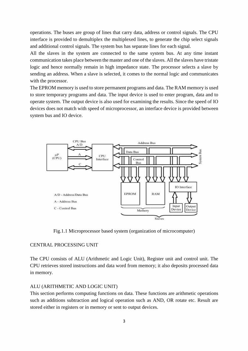
3
operations. The buses are group of lines that carry data, address or control signals. The CPU
interface is provided to demultiplex the multiplexed lines, to generate the chip select signals
and additional control signals. The system bus has separate lines for each signal.
All the slaves in the system are connected to the same system bus. At any time instant
communication takes place between the master and one of the slaves. All the slaves have tristate
logic and hence normally remain in high impedance state. The processor selects a slave by
sending an address. When a slave is selected, it comes to the normal logic and communicates
with the processor.
The EPROM memory is used to store permanent programs and data. The RAM memory is used
to store temporary programs and data. The input device is used to enter program, data and to
operate system. The output device is also used for examining the results. Since the speed of IO
devices does not match with speed of microprocessor, an interface device is provided between
system bus and IO device.
Fig.1.1 Microprocessor based system (organization of microcomputer)
CENTRAL PROCESSING UNIT
The CPU consists of ALU (Arithmetic and Logic Unit), Register unit and control unit. The
CPU retrieves stored instructions and data word from memory; it also deposits processed data
in memory.
ALU (ARITHMETIC AND LOGIC UNIT)
This section performs computing functions on data. These functions are arithmetic operations
such as additions subtraction and logical operation such as AND, OR rotate etc. Result are
stored either in registers or in memory or sent to output devices.
4
REGISTER UNIT
It contains various register. The registers are used primarily to store data temporarily during
the execution of a program. Some of the registers are accessible to the uses through instructions.
CONTROL UNIT
It provides necessary timing & control signals necessary to all the operations in the
microcomputer. It controls the flow of data between the p and peripherals (input, output &
memory). The control unit gets a clock which determines the speed of the p.
The CPU basic functions
It fetches an instructions word stored in memory.
It determines what the instruction is telling it to do.(decodes the instruction)
It executes the instruction. Executing the instruction may include some of the following major
tasks.
Transfer of data from reg. to reg. in the CPU itself.
Transfer of data between a CPU reg. & specified memory location.
Performing arithmetic and logical operations on data from a specific memory location or a
designated CPU register.
Directing the CPU to change a sequence of fetching instruction, if processing the data created
a specific condition.
Performing housekeeping function within the CPU itself inorder to establish desired condition
at certain registers.
It looks for control signal such as interrupts and provides appropriate responses.
It provides states, control, and timing signals that the memory and input/output section can use.
There are three buses:
ADDRESS BUS:
It is a group of wires or lines that are used to transfer the addresses of Memory or I/O devices.
It is unidirectional. In Intel 8085 microprocessor, Address bus was of 16 bits. This means that
Microprocessor 8085 can transfer maximum 16 bit address which means it can address 65,536
different memory locations. This bus is multiplexed with 8 bit data bus. So the most significant
bits (MSB) of address goes through Address bus (A7-A0) and LSB goes through multiplexed
data bus (AD0-AD7).
DATA BUS:
Data Bus is used to transfer data within Microprocessor and Memory/Input or Output devices.
It is bidirectional as Microprocessor requires to send or receive data. The data bus also works
5
as address bus when multiplexed with lower order address bus. Data bus is 8 Bits long. The
word length of a processor depends on data bus, thats why Intel 8085 is called 8 bit
Microprocessor because it have an 8 bit data bus.
CONTROL BUS:
Microprocessor uses control bus to process data that is what to do with the selected memory
location. Some control signals are Read, Write and Opcode fetch etc. Various operations are
performed by microprocessor with the help of control bus. This is a dedicated bus, because all
timing signals are generated according to control signal. The microprocessor is the master,
which controls all the activities of the system. To perform a specific job or task, the
microprocessor has to execute a program stored in memory. The program consists of a set of
instructions stored in consecutive memory location. In order to execute the program the
microprocessor issues address and control signals, to fetch the instruction and data from
memory one by one. After fetching each instruction it decodes the instruction and carries out
the task specified by the instruction.
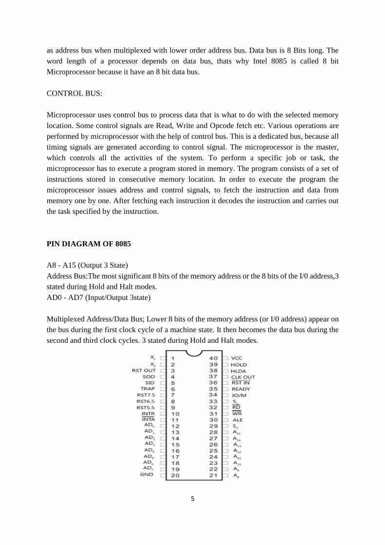
PIN DIAGRAM OF 8085
A8 - A15 (Output 3 State)
Address Bus:The most significant 8 bits of the memory address or the 8 bits of the I/0 address,3
stated during Hold and Halt modes.
AD0 - AD7 (Input/Output 3state)
Multiplexed Address/Data Bus; Lower 8 bits of the memory address (or I/0 address) appear on
the bus during the first clock cycle of a machine state. It then becomes the data bus during the
second and third clock cycles. 3 stated during Hold and Halt modes.
6
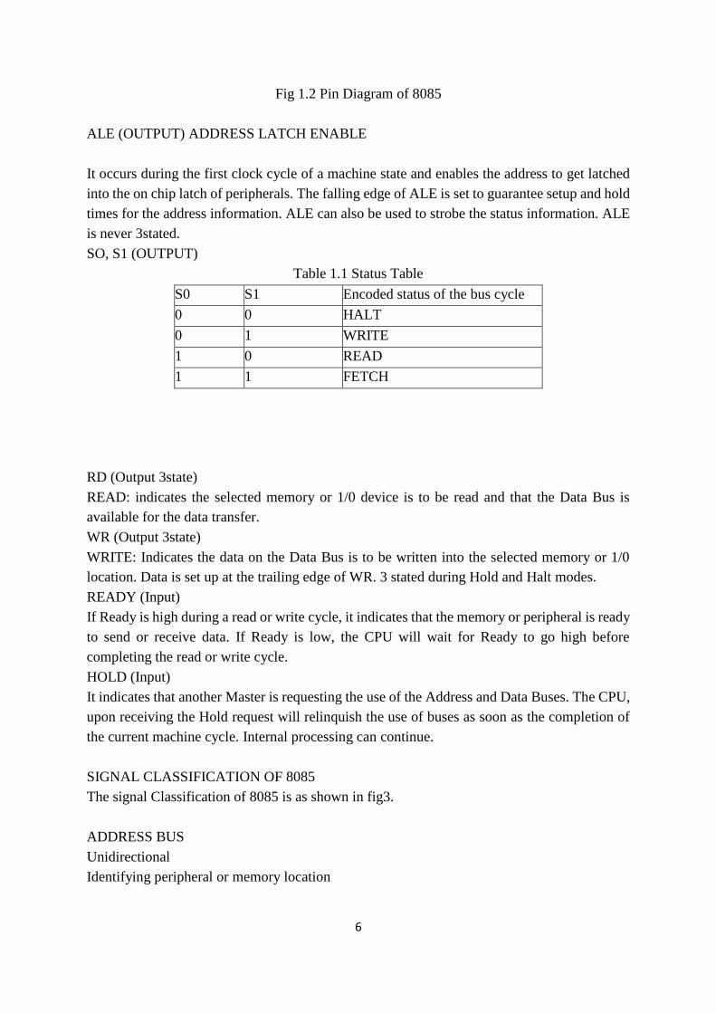
Fig 1.2 Pin Diagram of 8085
ALE (OUTPUT) ADDRESS LATCH ENABLE
It occurs during the first clock cycle of a machine state and enables the address to get latched
into the on chip latch of peripherals. The falling edge of ALE is set to guarantee setup and hold
times for the address information. ALE can also be used to strobe the status information. ALE
is never 3stated.
SO, S1 (OUTPUT)
Table 1.1 Status Table
S0 S1 Encoded status of the bus cycle
0 0 HALT
0 1 WRITE
1 0 READ
1 1 FETCH
RD (Output 3state)
READ: indicates the selected memory or 1/0 device is to be read and that the Data Bus is
available for the data transfer.
WR (Output 3state)
WRITE: Indicates the data on the Data Bus is to be written into the selected memory or 1/0
location. Data is set up at the trailing edge of WR. 3 stated during Hold and Halt modes.
READY (Input)
If Ready is high during a read or write cycle, it indicates that the memory or peripheral is ready
to send or receive data. If Ready is low, the CPU will wait for Ready to go high before
completing the read or write cycle.
HOLD (Input)
It indicates that another Master is requesting the use of the Address and Data Buses. The CPU,
upon receiving the Hold request will relinquish the use of buses as soon as the completion of
the current machine cycle. Internal processing can continue.
SIGNAL CLASSIFICATION OF 8085
The signal Classification of 8085 is as shown in fig3.
ADDRESS BUS
Unidirectional
Identifying peripheral or memory location

7
DATA BUS
Bidirectional
Transferring data
CONTROL BUS
Synchronization signals
Timing signals
Control signal
Fig: 1.3 Signal Classifications of 8085 System Bus
ARCHITECTURE OF INTEL 8085 MICROPROCESSOR
The architecture of INTEL 8085 microprocessor is as shown in fig1.4.
THE ALU
In addition to the arithmetic & logic circuits, the ALU includes the accumulator, which is part
of every arithmetic & logic operation.
Also, the ALU includes a temporary register used for holding data temporarily during the
execution of the operation. This temporary register is not accessible by the programmer.
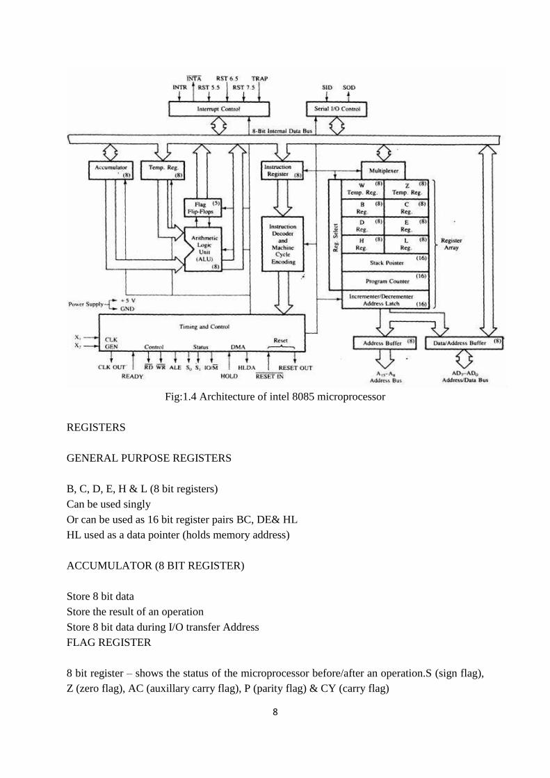
8
Fig:1.4 Architecture of intel 8085 microprocessor
REGISTERS
GENERAL PURPOSE REGISTERS
B, C, D, E, H & L (8 bit registers)
Can be used singly
Or can be used as 16 bit register pairs BC, DE& HL
HL used as a data pointer (holds memory address)
ACCUMULATOR (8 BIT REGISTER)
Store 8 bit data
Store the result of an operation
Store 8 bit data during I/O transfer Address
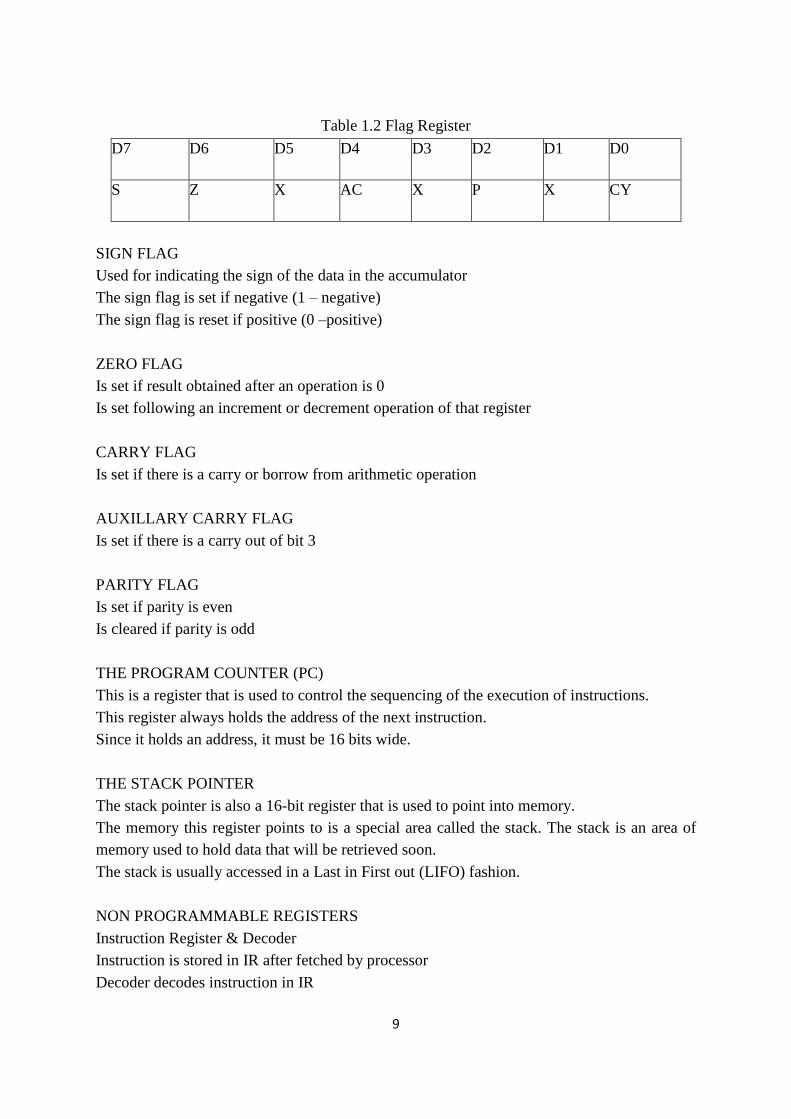
FLAG REGISTER
8 bit register – shows the status of the microprocessor before/after an operation.S (sign flag),
Z (zero flag), AC (auxillary carry flag), P (parity flag) & CY (carry flag)
9
Table 1.2 Flag Register
D7 D6 D5 D4 D3 D2 D1 D0
S Z X AC X P X CY
SIGN FLAG
Used for indicating the sign of the data in the accumulator
The sign flag is set if negative (1 – negative)
The sign flag is reset if positive (0 –positive)
ZERO FLAG
Is set if result obtained after an operation is 0
Is set following an increment or decrement operation of that register
CARRY FLAG
Is set if there is a carry or borrow from arithmetic operation
AUXILLARY CARRY FLAG
Is set if there is a carry out of bit 3
PARITY FLAG
Is set if parity is even
Is cleared if parity is odd
THE PROGRAM COUNTER (PC)
This is a register that is used to control the sequencing of the execution of instructions.
This register always holds the address of the next instruction.
Since it holds an address, it must be 16 bits wide.
THE STACK POINTER
The stack pointer is also a 16-bit register that is used to point into memory.
The memory this register points to is a special area called the stack. The stack is an area of
memory used to hold data that will be retrieved soon.
The stack is usually accessed in a Last in First out (LIFO) fashion.
NON PROGRAMMABLE REGISTERS
Instruction Register & Decoder
Instruction is stored in IR after fetched by processor
Decoder decodes instruction in IR
10
INTERNAL CLOCK GENERATOR
3.125 MHz internally
6.25 MHz externally
THE ADDRESS AND DATA BUSSES
The address bus has 8 signal lines A8 – A15 which are unidirectional.
The other 8 address bits are multiplexed (time shared) with the 8 data bits.
So, the bits AD0 – AD7 are bi-directional and serve as A0 – A7 and D0 – D7 at the same time.
During the xecution of the instruction, these lines carry the address bits during the early part,
then during the late parts of the execution, they carry the 8 data bits.
In order to separate the address from the data, we can use a latch to save the value before the
function of the bits changes.
DEMULTIPLEXING AD7-AD0
From the above description, it becomes obvious that the AD7– AD0 lines are serving a dual
purpose and that they need to be demultiplexed to get all the information.
The high order bits of the address remain on the bus for three clock periods. However, the low
order bits remain for only one clock period and they would be lost if they are not saved
externally. Also, notice that the low order bits of the address disappear when they are needed
most.
To make sure we have the entire address for the full three clock cycles, we will use an external
latch to save the value of AD7– AD0 when it is carrying the address bits. We use the ALE
signal to enable this latch.
DEMULTIPLEXING AD7-AD0
Given that ALE operates as a pulse during T1, we will be able to latch the address. Then when
ALE goes low, the address is saved and the AD7– AD0 lines can be used for their purpose as
the bi-directional data lines.
DEMULTIPLEXING THE BUS AD7 – AD0
The high order address is placed on the address bus and hold for 3 clk periods.
The low order address is lost after the first clk period, this address needs to be hold however
we need to use latch
The address AD7 – AD0 is connected as inputs to the latch 74LS373.
The ALE signal is connected to the enable (G) pin of the latch and the OC – Output control –
of the latch is grounded
ADDRESSING MODES
The microprocessor has different ways of specifying the data for the instruction. These are
called addressing modes.
11
The 8085 has four addressing modes:
Implied CMA
Immediate MVI B, 45
Direct LDA 4000
Indirect LDAX B
Load the accumulator with the contents of the memory location whose address is stored in the
register pair BC).
Many instructions require two operands for execution. For example transfer of data between
two registers. The method of identifying the operands position by the instruction format is
known as the addressing mode. When two operands are involved in an instruction, the first
operand is assumed to be in a register Mp itself.
Types of Addressing Modes
Register addressing
Direct addressing mode
Register indirect addressing
Immediate Addressing mode
Implied addressing mode
REGISTER ADDRESSING
This type of addressing mode specifies register or register pair that contains data.ie (only the
register need be specified as the address of the operands).
Example MOV B, A (the content of A is copied into the register B)
DIRECT ADDRESSING MODE
Data is directly copied from the given address to the register.
Example LDA 3000H (The content at the location 3000H is copied to the register A).
REGISTER INDIRECT ADDRESSING
In this mode, the address of operand is specified by a register pair
Example MOV A, M (Move data from memory location specified by H-L pair to accumulator)
IMMEDIATE ADDRESSING MODE
In this mode, the operand is specified within the instruction itself. Example MVI A, 05 H
(Move 05 H in accumulator.)
12
IMPLIED ADDRESSING MODE
This mode doesn't require any operand. The data is specified by opcode itself. Example
RAL, CMP
TIMING DIAGRAM
Timing diagram is the display of initiation of read/write and transfer of data operations under
the control of 3-status signals IO / M, S1, and S0. All actions in the microprocessor are
controlled by either leading or trailing edge of the clock.
MACHINE CYCLE
It is the time required by the microprocessor to complete the operation of accessing the memory
devices or I/O devices. In machine cycle various operations like opcode fetch, memory read,
memory write, I/O read, I/O write are performed.
T-STATE
Each clock cycle is called as T-states.
Each machine cycle is composed of many clock cycles. Since, the data and instructions, both
are stored in the memory, the µP performs fetch operation to read the instruction or data and
then execute the instruction. The 3-status signals: IO / M, S1, and S0 are generated at the
beginning of each machine cycle. The unique combination of these 3-status signals identify
read or write operation and remain valid for the duration of the cycle.
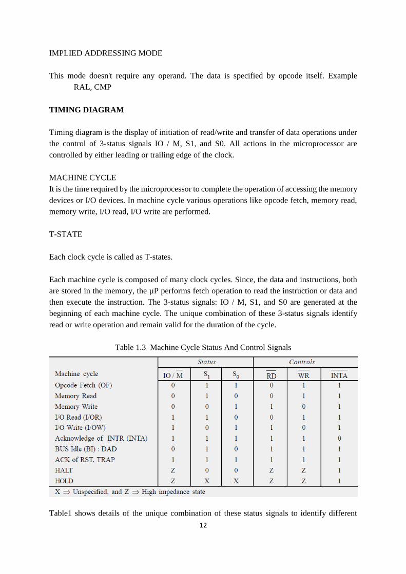
Table 1.3 Machine Cycle Status And Control Signals
Table1 shows details of the unique combination of these status signals to identify different
13
machine cycles. Thus, time taken by any µP to execute one instruction is calculated in terms
of the clock period. The execution of instruction always requires read and writes operations to
transfer data to or from the µP and memory or I/O devices. Each read/ write operation
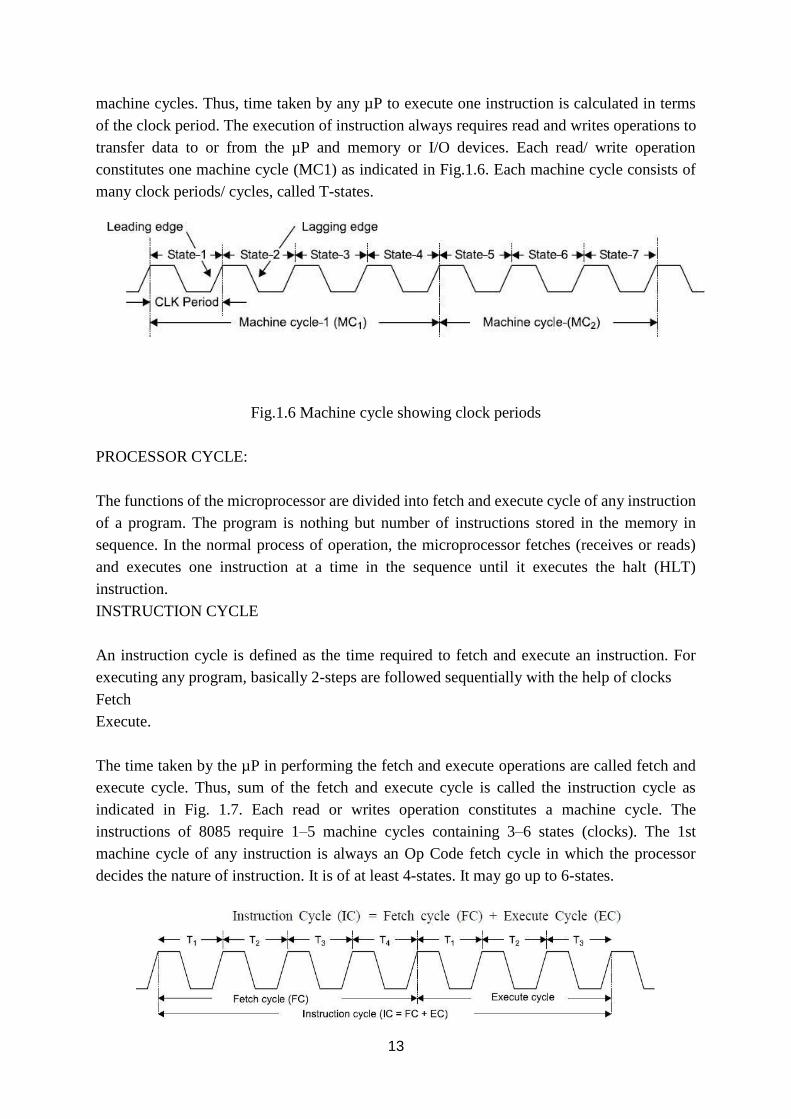
constitutes one machine cycle (MC1) as indicated in Fig.1.6. Each machine cycle consists of
many clock periods/ cycles, called T-states.
Fig.1.6 Machine cycle showing clock periods
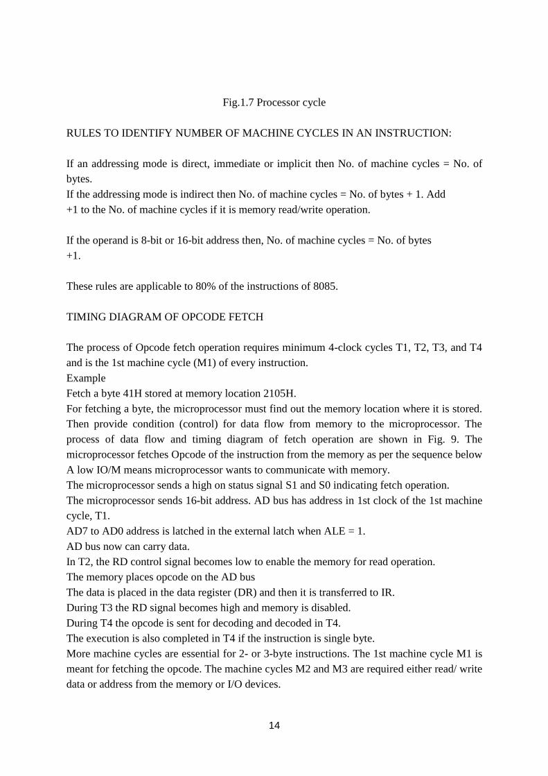
PROCESSOR CYCLE:
The functions of the microprocessor are divided into fetch and execute cycle of any instruction
of a program. The program is nothing but number of instructions stored in the memory in
sequence. In the normal process of operation, the microprocessor fetches (receives or reads)
and executes one instruction at a time in the sequence until it executes the halt (HLT)
instruction.
INSTRUCTION CYCLE
An instruction cycle is defined as the time required to fetch and execute an instruction. For
executing any program, basically 2-steps are followed sequentially with the help of clocks
Fetch
Execute.
The time taken by the µP in performing the fetch and execute operations are called fetch and
execute cycle. Thus, sum of the fetch and execute cycle is called the instruction cycle as
indicated in Fig. 1.7. Each read or writes operation constitutes a machine cycle. The
instructions of 8085 require 1–5 machine cycles containing 3–6 states (clocks). The 1st
machine cycle of any instruction is always an Op Code fetch cycle in which the processor
decides the nature of instruction. It is of at least 4-states. It may go up to 6-states.
14
Fig.1.7 Processor cycle
RULES TO IDENTIFY NUMBER OF MACHINE CYCLES IN AN INSTRUCTION:
If an addressing mode is direct, immediate or implicit then No. of machine cycles = No. of
bytes.
If the addressing mode is indirect then No. of machine cycles = No. of bytes + 1. Add
+1 to the No. of machine cycles if it is memory read/write operation.
If the operand is 8-bit or 16-bit address then, No. of machine cycles = No. of bytes
+1.
These rules are applicable to 80% of the instructions of 8085.
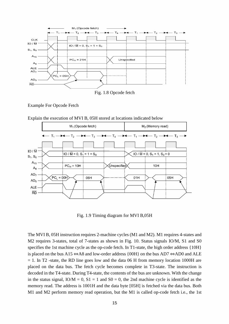
TIMING DIAGRAM OF OPCODE FETCH
The process of Opcode fetch operation requires minimum 4-clock cycles T1, T2, T3, and T4
and is the 1st machine cycle (M1) of every instruction.
Example
Fetch a byte 41H stored at memory location 2105H.
For fetching a byte, the microprocessor must find out the memory location where it is stored.
Then provide condition (control) for data flow from memory to the microprocessor. The
process of data flow and timing diagram of fetch operation are shown in Fig. 9. The
microprocessor fetches Opcode of the instruction from the memory as per the sequence below
A low IO/M means microprocessor wants to communicate with memory.
The microprocessor sends a high on status signal S1 and S0 indicating fetch operation.
The microprocessor sends 16-bit address. AD bus has address in 1st clock of the 1st machine
cycle, T1.
AD7 to AD0 address is latched in the external latch when ALE = 1.
AD bus now can carry data.
In T2, the RD control signal becomes low to enable the memory for read operation.
The memory places opcode on the AD bus
The data is placed in the data register (DR) and then it is transferred to IR.
During T3 the RD signal becomes high and memory is disabled.
During T4 the opcode is sent for decoding and decoded in T4.
The execution is also completed in T4 if the instruction is single byte.
More machine cycles are essential for 2- or 3-byte instructions. The 1st machine cycle M1 is
meant for fetching the opcode. The machine cycles M2 and M3 are required either read/ write
data or address from the memory or I/O devices.
15
Fig. 1.8 Opcode fetch
Example For Opcode Fetch
Explain the execution of MVI B, 05H stored at locations indicated below
Fig. 1.9 Timing diagram for MVI B,05H
The MVI B, 05H instruction requires 2-machine cycles (M1 and M2). M1 requires 4-states and
M2 requires 3-states, total of 7-states as shown in Fig. 10. Status signals IO/M, S1 and S0
specifies the 1st machine cycle as the op-code fetch. In T1-state, the high order address {10H}
is placed on the bus A15 ⇔A8 and low-order address {00H} on the bus AD7 ⇔AD0 and ALE
= 1. In T2 -state, the RD line goes low and the data 06 H from memory location 1000H are
placed on the data bus. The fetch cycle becomes complete in T3-state. The instruction is
decoded in the T4-state. During T4-state, the contents of the bus are unknown. With the change
in the status signal, IO/M = 0, S1 = 1 and S0 = 0, the 2nd machine cycle is identified as the
memory read. The address is 1001H and the data byte [05H] is fetched via the data bus. Both
M1 and M2 perform memory read operation, but the M1 is called op-code fetch i.e., the 1st
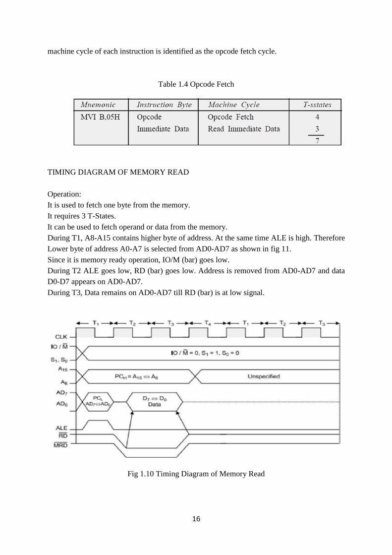
16
machine cycle of each instruction is identified as the opcode fetch cycle.
Table 1.4 Opcode Fetch
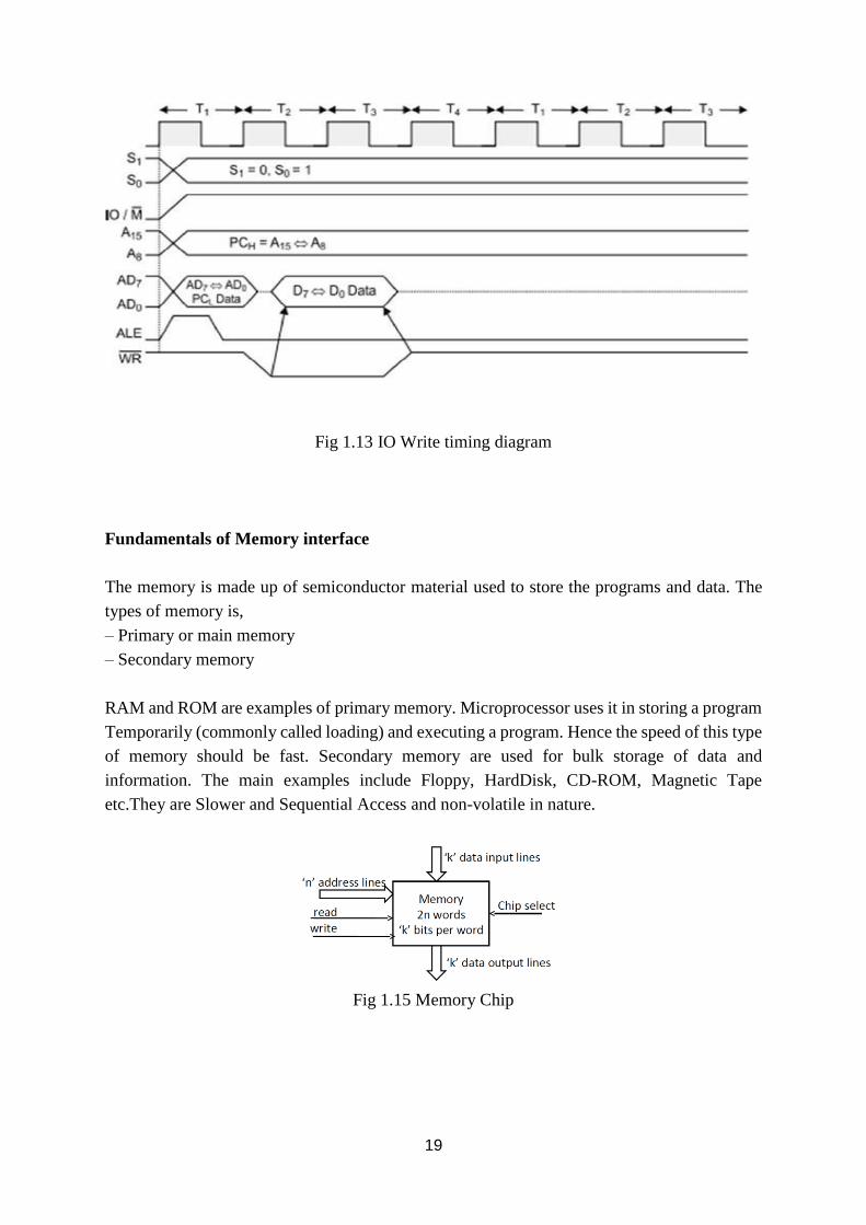
TIMING DIAGRAM OF MEMORY READ
Operation:
It is used to fetch one byte from the memory.
It requires 3 T-States.
It can be used to fetch operand or data from the memory.
During T1, A8-A15 contains higher byte of address. At the same time ALE is high. Therefore
Lower byte of address A0-A7 is selected from AD0-AD7 as shown in fig 11.
Since it is memory ready operation, IO/M (bar) goes low.
During T2 ALE goes low, RD (bar) goes low. Address is removed from AD0-AD7 and data
D0-D7 appears on AD0-AD7.
During T3, Data remains on AD0-AD7 till RD (bar) is at low signal.
Fig 1.10 Timing Diagram of Memory Read

17
TIMING DIAGRAM FOR MEMORY WRITE
Operation:
It is used to send one byte into memory.
It requires 3 T-States.
During T1, ALE is high and contains lower address A0-A7 from AD0-AD7.
A8-A15 contains higher byte of address.
As it is memory operation, IO/M (bar) goes low.
During T2, ALE goes low, WR (bar) goes low and Address is removed from AD0- AD7 and
then data appears on AD0-AD7 as in fig 12.
Data remains on AD0-AD7 till WR (bar) is low.
Fig 1.11 Memory Write timing diagram
TIMING DIAGRAM OF IO READ
Operation:
It is used to fetch one byte from an IO port.
It requires 3 T-States.
During T1, The Lower Byte of IO address is duplicated into higher order address bus A8-A15
as in fig13.
ALE is high and AD0-AD7 contains address of IO device.

18
IO/M (bar) goes high as it is an IO operation.
During T2, ALE goes low, RD (bar) goes low and data appears on AD0-AD7 as input from IO
device.
During T3 Data remains on AD0-AD7 till RD (bar) is low.
Fig 1.12 IO Read timing diagram
TIMING DIAGRAM OF IO WRITE
Operation:
It is used to writ one byte into IO device.
It requires 3 T-States.
During T1, the lower byte of address is duplicated into higher order address bus A8- A15 as in
fig 14.
ALE is high and A0-A7 address is selected from AD0-AD7.
As it is an IO operation IO/M (bar) goes low.
During T2, ALE goes low, WR (bar) goes low and data appears on AD0-AD7 to write data
into IO device.
During T3, Data remains on AD0-AD7 till WR(bar) is low.
19
Fig 1.13 IO Write timing diagram
Fundamentals of Memory interface
The memory is made up of semiconductor material used to store the programs and data. The
types of memory is,
– Primary or main memory
– Secondary memory
RAM and ROM are examples of primary memory. Microprocessor uses it in storing a program
Temporarily (commonly called loading) and executing a program. Hence the speed of this type
of memory should be fast. Secondary memory are used for bulk storage of data and
information. The main examples include Floppy, HardDisk, CD-ROM, Magnetic Tape
etc.They are Slower and Sequential Access and non-volatile in nature.
Fig 1.15 Memory Chip
20
Fig 1.14 8085 Interfacing with Memory chips
Fig 1.15 Interface with two memory chips
In case of multiple chips simple circuit like NOT gate will not work. In this case normally
decoder circuits like 3-to-8 decoder circuit 74LS138 are used. These circuit are called address
decoders.
Fig 1.16 Address Decoders
21
There are two types of address decoding techniques
– Exhaustive Decoding
– Partial Decoding
In Exhaustive Decoding all the 16 bits of the 8085 address bus are used to select a particular
location in memory chip.
• Advantages:
– Complete Address Utilization
– Ease in Future Expansion
– No Bus Contention, as all addresses are unique.
• Disadvantages
– Increased hardware and cost.
– Speed is less due to increased delay.
In this scheme minimum number of address lines are used as required to select a memory
location in chip.
• Advantages:
– Simple, Cheap and Fast.
• Disadvantages:
– Unutilized space & fold back (multiple mapping).
– Bus Contention.
– Difficult future expansion.
TEXT / REFERENCE BOOKS
1. Ramesh Goankar, "Microprocessor architecture programming and applications with
8085 / 8088", 5th Edition, Penram International Publishing.
2. A.K.Ray and Bhurchandi, "Advanced Microprocessor", 1st Edition, TMH
Publication.
3. Kenneth J.Ayala, "The 8051 microcontroller Architecture, Programming and
applications" 2nd Edition ,Penram international.
4. Doughlas V.Hall, "Microprocessors and Digital system", 2nd Editon, Mc Graw
Hill,1983.
5. Md.Rafiquzzaman, "Microprocessors and Microcomputer based system design",
2nd Editon,Universal Book Stall, 1992.
6. Hardware Reference Manual for 80X86 family", Intel Corporation, 1990.
22
Question Bank
Part A
1. What is Microprocessor? Give the power supply & clock frequency of 8085 2. What are the functions of an accumulator? 3. List the 16 – bit registers of 8085 microprocessor 4. List few applications of microprocessor-based system 5. List the allowed register pairs of 8085 6. Mention the purpose of SID and SOD lines 7. What is an Opcode? 8. What is the function of IO/M signal in the 8085? 9. What is an Operand?
Part B
1. Explain the architecture of 8085 microprocessor in detail with the help of neat diagram.
2. Explain the timing diagram of Opcode fetch cycle.
3. Explain the timing diagram of memory write cycle with example. 4. Define addressing modes. With suitable examples explain 8085 addressing modes in
detail.
23
SCHOOL OF COMPUTING
DEPARTMENT OF COMPUTER SCIENCE ENGINEERING
UNIT – II – 8085 Instruction Set and Assembly Language Programming -SECA1404
– SECA1404
24
II. 8085 Instruction Set and Assembly Language
Programming
An instruction is a binary pattern designed inside a microprocessor to perform a specific
function.
The entire group of instructions that a microprocessor supports is called
Instruction Set.
8085 has 246 instructions.
Each instruction is represented by an 8-bit binary value.
These 8-bits of binary value is called Op-Code or Instruction Byte.
Classification of Instruction Set
Data Transfer Instruction
Arithmetic Instructions
Logical Instructions
Branching Instructions
Control Instructions
Data Transfer Instruction
These instructions move data between registers, or between memory and registers.
These instructions copy data from source to destination.
While copying, the contents of source are not modified.
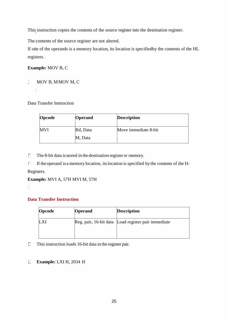
Opcode Operand Description
MOV Rd, Rs Rd,
M M, Rs
Copy from source to destination.
25
This instruction copies the contents of the source register into the destination register.
The contents of the source register are not altered.
If one of the operands is a memory location, its location is specifiedby the contents of the HL
registers.
Example: MOV B, C
MOV B, M MOV M, C
Data Transfer Instruction
Opcode Operand Description
MVI Rd, Data
M, Data
Move immediate 8-bit
The 8-bit data is stored in the destination register or memory.
If the operand is a memory location, its location is specified by the contents of the H-
Registers.
Example: MVI A, 57H MVI M, 57H
Data Transfer Instruction
Opcode Operand Description
LXI Reg. pair, 16-bit data Load register pair immediate
This instruction loads 16-bit data in the register pair.
Example: LXI H, 2034 H
26
Data Transfer Instruction
Opcode Operand Description
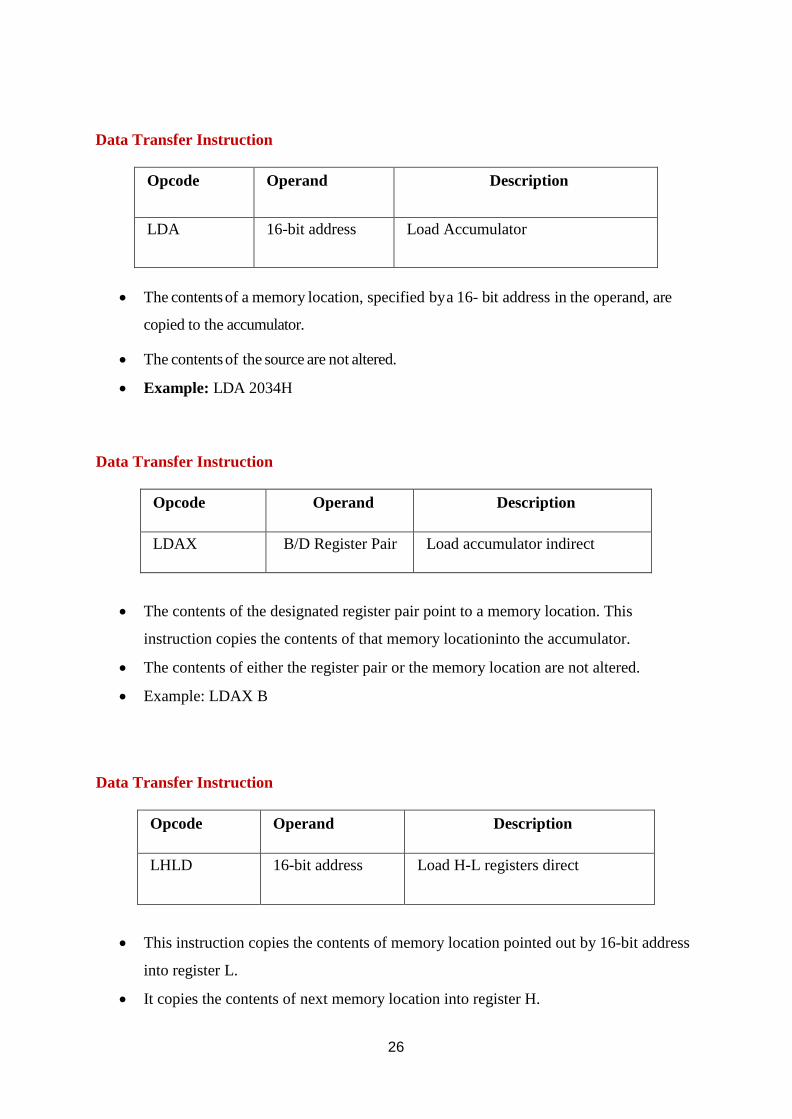
LDA 16-bit address Load Accumulator
The contents of a memory location, specified by a 16- bit address in the operand, are
copied to the accumulator.
The contents of the source are not altered.
Example: LDA 2034H
Data Transfer Instruction
Opcode Operand Description
LDAX B/D Register Pair Load accumulator indirect
The contents of the designated register pair point to a memory location. This
instruction copies the contents of that memory locationinto the accumulator.
The contents of either the register pair or the memory location are not altered.
Example: LDAX B
Data Transfer Instruction
Opcode Operand Description
LHLD 16-bit address Load H-L registers direct
This instruction copies the contents of memory location pointed out by 16-bit address
into register L.
It copies the contents of next memory location into register H.
27
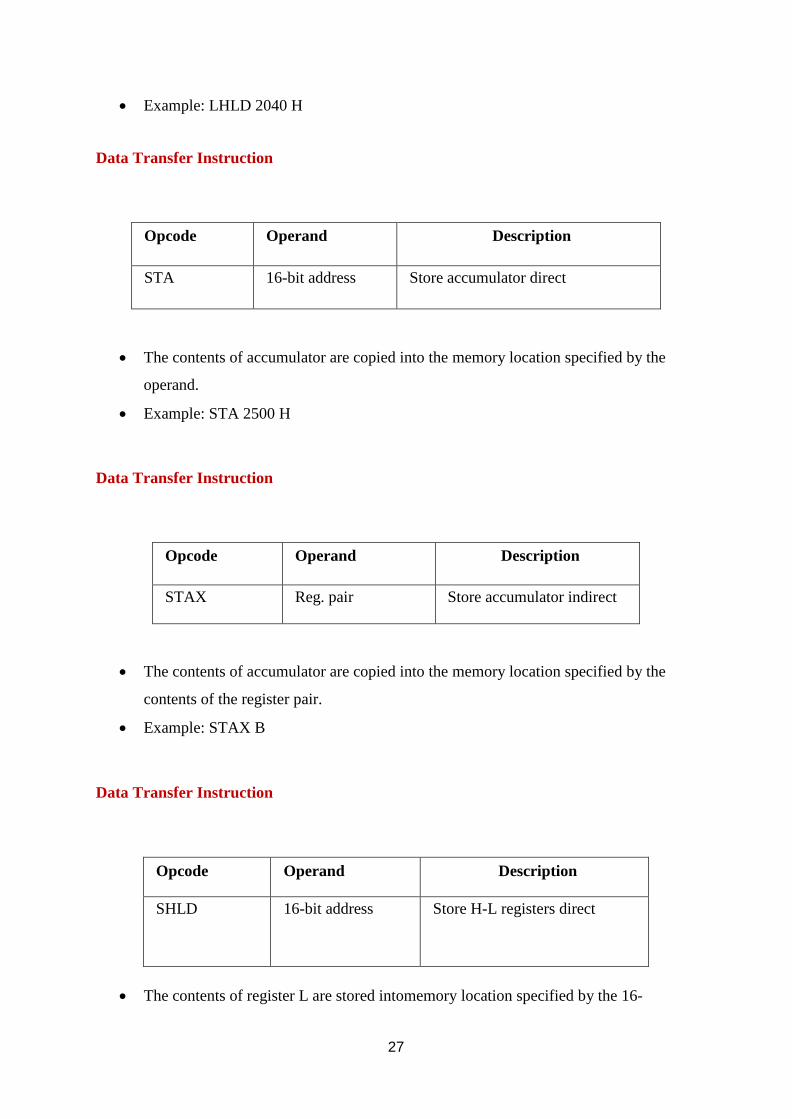
Example: LHLD 2040 H
Data Transfer Instruction
Opcode Operand Description
STA 16-bit address Store accumulator direct
The contents of accumulator are copied into the memory location specified by the
operand.
Example: STA 2500 H
Data Transfer Instruction
Opcode Operand Description
STAX Reg. pair Store accumulator indirect
The contents of accumulator are copied into the memory location specified by the
contents of the register pair.
Example: STAX B
Data Transfer Instruction
Opcode Operand Description
SHLD 16-bit address Store H-L registers direct
The contents of register L are stored intomemory location specified by the 16-
28
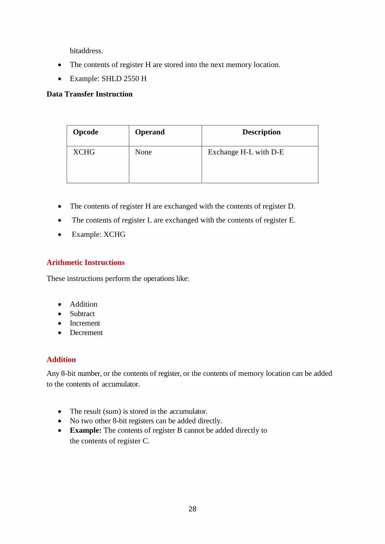
bitaddress.
The contents of register H are stored into the next memory location.
Example: SHLD 2550 H
Data Transfer Instruction
Opcode Operand Description
XCHG None Exchange H-L with D-E
The contents of register H are exchanged with the contents of register D.
The contents of register L are exchanged with the contents of register E.
Example: XCHG
Arithmetic Instructions
These instructions perform the operations like:
Addition
Subtract
Increment
Decrement
Addition
Any 8-bit number, or the contents of register, or the contents of memory location can be added
to the contents of accumulator.
The result (sum) is stored in the accumulator.
No two other 8-bit registers can be added directly.
Example: The contents of register B cannot be added directly to
the contents of register C.

29
Subtract Any 8-bit number, or the contents of register, or the contents of memory location can be subtracted from
the contents of accumulator.
The result is stored in the accumulator.
Subtraction is performed in 2’s complement form.
If the result is negative, it is stored in 2’s complement form.
No two other 8-bit registers can be subtracted directly.
Increment/Decrement
The 8-bit contents of a register or a memory location can be incremented or decremented by 1.
The 16-bit contents of a register pair can be incremented or decremented by 1.
Increment or decrement can be performed on any register or a memory location.
Arithmetic Instructions
Opcode
Operand Description
ADD R, M Add register or memory to accumulator
The contents of register or memory are added to the contents of accumulator.
The result is stored in accumulator.
If the operand is memory location, its address is specified by H-L pair.
All flags are modified to reflect the result of the addition.
Example: ADD B or ADD M
30
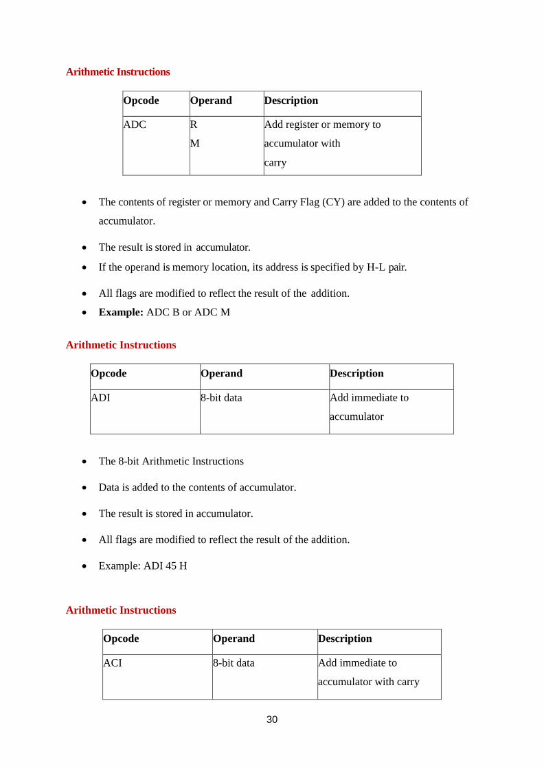
Arithmetic Instructions
Opcode Operand Description
ADC R
M
Add register or memory to
accumulator with
carry
The contents of register or memory and Carry Flag (CY) are added to the contents of
accumulator.
The result is stored in accumulator.
If the operand is memory location, its address is specified by H-L pair.
All flags are modified to reflect the result of the addition.
Example: ADC B or ADC M
Arithmetic Instructions
Opcode Operand Description
ADI 8-bit data Add immediate to
accumulator
The 8-bit Arithmetic Instructions
Data is added to the contents of accumulator.
The result is stored in accumulator.
All flags are modified to reflect the result of the addition.
Example: ADI 45 H
Arithmetic Instructions
Opcode Operand Description
ACI 8-bit data Add immediate to
accumulator with carry
31
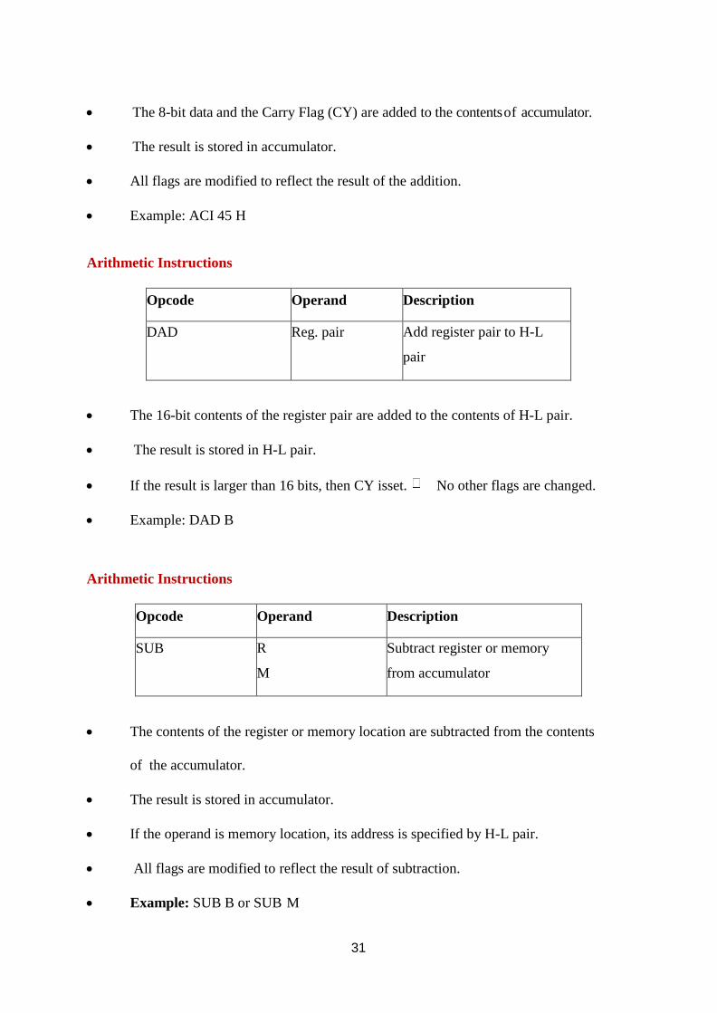
The 8-bit data and the Carry Flag (CY) are added to the contents of accumulator.
The result is stored in accumulator.
All flags are modified to reflect the result of the addition.
Example: ACI 45 H
Arithmetic Instructions
Opcode Operand Description
DAD Reg. pair Add register pair to H-L
pair
The 16-bit contents of the register pair are added to the contents of H-L pair.
The result is stored in H-L pair.
If the result is larger than 16 bits, then CY isset. No other flags are changed.
Example: DAD B
Arithmetic Instructions
Opcode Operand Description
SUB R
M
Subtract register or memory
from accumulator
The contents of the register or memory location are subtracted from the contents
of the accumulator.
The result is stored in accumulator.
If the operand is memory location, its address is specified by H-L pair.
All flags are modified to reflect the result of subtraction.
Example: SUB B or SUB M
32
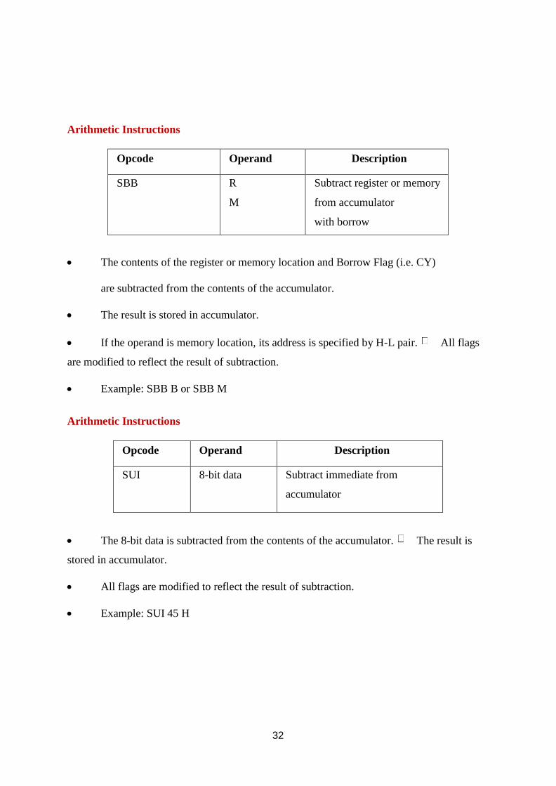
Arithmetic Instructions
Opcode Operand Description
SBB R
M
Subtract register or memory
from accumulator
with borrow
The contents of the register or memory location and Borrow Flag (i.e. CY)
are subtracted from the contents of the accumulator.
The result is stored in accumulator.
If the operand is memory location, its address is specified by H-L pair. All flags
are modified to reflect the result of subtraction.
Example: SBB B or SBB M
Arithmetic Instructions
Opcode Operand Description
SUI 8-bit data Subtract immediate from
accumulator
The 8-bit data is subtracted from the contents of the accumulator. The result is
stored in accumulator.
All flags are modified to reflect the result of subtraction.
Example: SUI 45 H
33
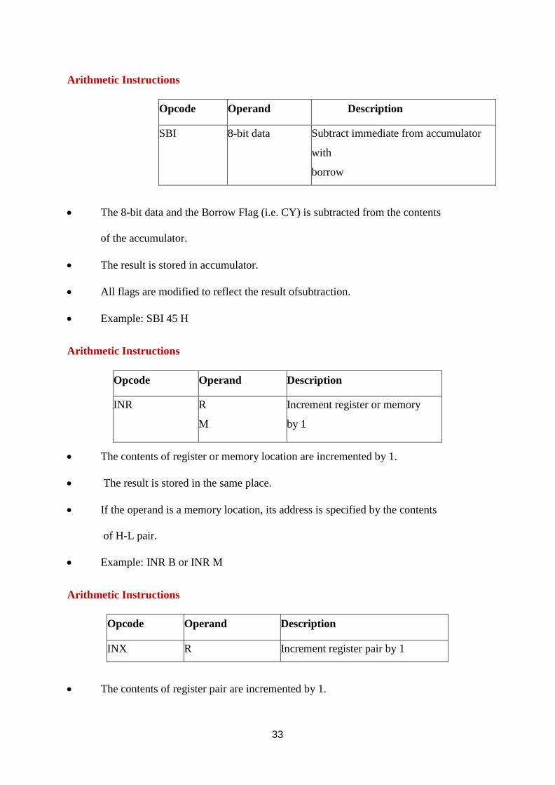
Arithmetic Instructions
Opcode Operand Description
SBI 8-bit data Subtract immediate from accumulator
with
borrow
The 8-bit data and the Borrow Flag (i.e. CY) is subtracted from the contents
of the accumulator.
The result is stored in accumulator.
All flags are modified to reflect the result ofsubtraction.
Example: SBI 45 H
Arithmetic Instructions
Opcode Operand Description
INR R
M
Increment register or memory
by 1
The contents of register or memory location are incremented by 1.
The result is stored in the same place.
If the operand is a memory location, its address is specified by the contents
of H-L pair.
Example: INR B or INR M
Arithmetic Instructions
Opcode Operand Description
INX R Increment register pair by 1
The contents of register pair are incremented by 1.
34
The result is stored in the same place.
Example: INX H
Arithmetic Instructions
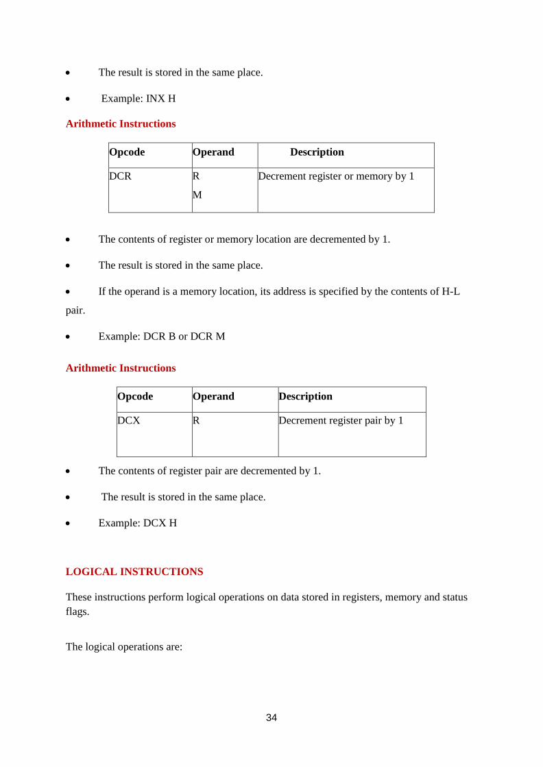
Opcode Operand Description
DCR R
M
Decrement register or memory by 1
The contents of register or memory location are decremented by 1.
The result is stored in the same place.
If the operand is a memory location, its address is specified by the contents of H-L
pair.
Example: DCR B or DCR M
Arithmetic Instructions
Opcode Operand Description
DCX R Decrement register pair by 1
The contents of register pair are decremented by 1.
The result is stored in the same place.
Example: DCX H
LOGICAL INSTRUCTIONS
These instructions perform logical operations on data stored in registers, memory and status
flags.
The logical operations are:
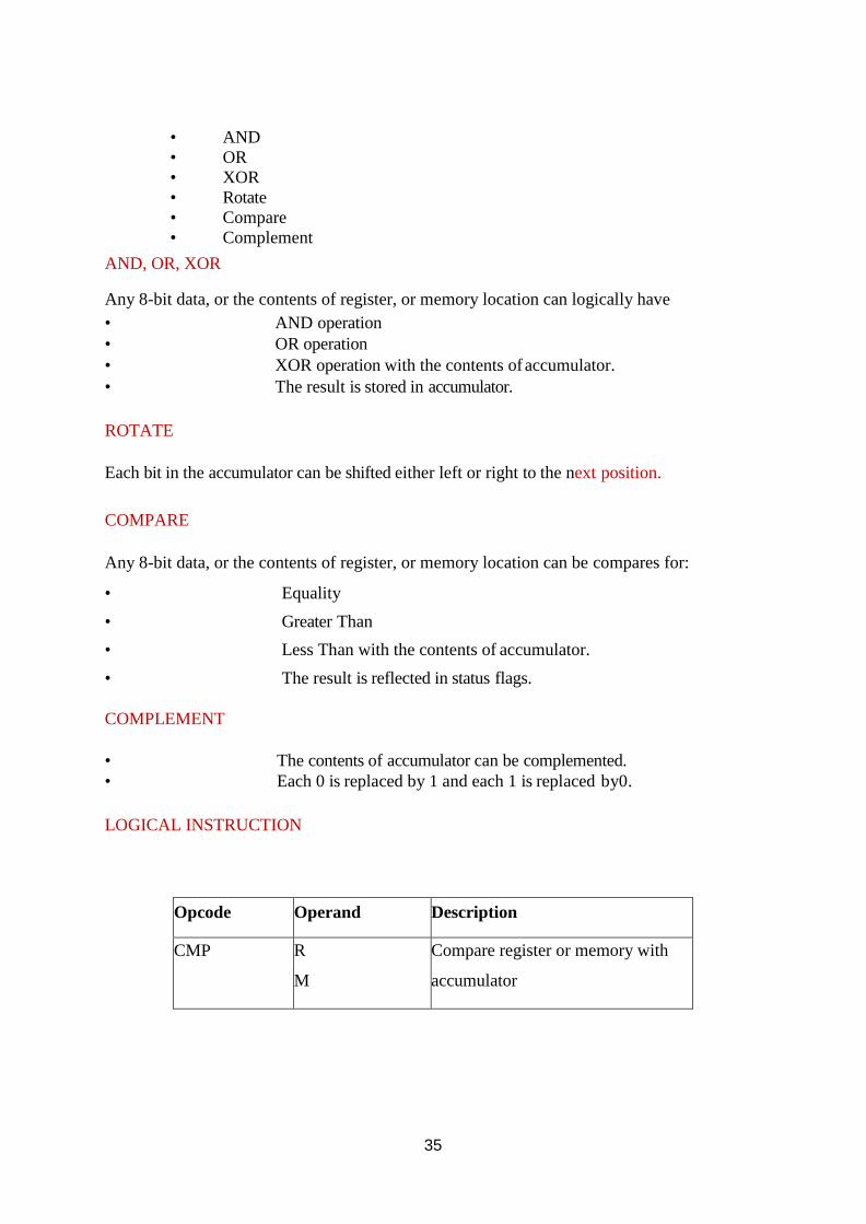
35
• AND
• OR
• XOR
• Rotate
• Compare
• Complement
AND, OR, XOR
Any 8-bit data, or the contents of register, or memory location can logically have
• AND operation
• OR operation
• XOR operation with the contents of accumulator.
• The result is stored in accumulator.
ROTATE
Each bit in the accumulator can be shifted either left or right to the next position.
COMPARE
Any 8-bit data, or the contents of register, or memory location can be compares for:
• Equality
• Greater Than
• Less Than with the contents of accumulator.
• The result is reflected in status flags.
COMPLEMENT
• The contents of accumulator can be complemented.
• Each 0 is replaced by 1 and each 1 is replaced by0.
LOGICAL INSTRUCTION
Opcode Operand Description
CMP R
M
Compare register or memory with
accumulator
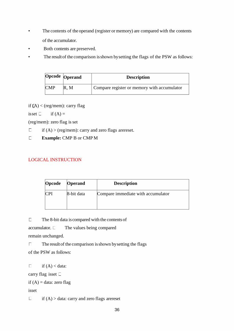
36
• The contents of the operand (register or memory) are compared with the contents
of the accumulator.
• Both contents are preserved.
• The result of the comparison is shown by setting the flags of the PSW as follows:
Opcode Operand Description
CMP R, M Compare register or memory with accumulator
if (A) < (reg/mem): carry flag
is set if (A) =
(reg/mem): zero flag is set
if (A) > (reg/mem): carry and zero flags arereset.
Example: CMP B or CMP M
LOGICAL INSTRUCTION
Opcode Operand Description
CPI 8-bit data Compare immediate with accumulator
The 8-bit data is compared with the contents of
accumulator. The values being compared
remain unchanged.
The result of the comparison is shown by setting the flags
of the PSW as follows:
if (A) < data:
carry flag isset
if (A) = data: zero flag
isset
if (A) > data: carry and zero flags arereset

37
Example: CPI 89H

38
LOGICAL INSTRUCTION
Opcode Operand Description
XRA R M Exclusive OR register or memory with
accumulator
The contents of the accumulator are XORed with the contents of the register or memory.
The result is placed in the accumulator.
If the operand is a memory location, its address is specified by the contents of H-L
pair.
S, Z, P are modified to reflect the result of the operation. CY and AC are reset.
Example: XRA B or XRA M.
LOGICAL INSTRUCTION
Opcode Operand Description
ORA R
M
Logical OR register or memory with accumulator
The contents of the accumulator are logically OR ed with the contents of the register or memory.
The result is placed in the accumulator.
If the operand is a memory location, its address is specified by the contents of H-L
pair.
S, Z, P are modified to reflect the result. CY and AC are reset.
Example: ORA B or ORA M.
39
LOGICAL INSTRUCTION
Opcode Operand Description
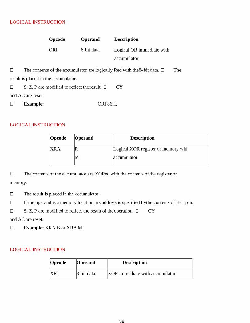
ORI 8-bit data Logical OR immediate with
accumulator
The contents of the accumulator are logically Red with the8- bit data. The
result is placed in the accumulator.
S, Z, P are modified to reflect the result. CY
and AC are reset.
Example: ORI 86H.
LOGICAL INSTRUCTION
Opcode Operand Description
XRA R
M
Logical XOR register or memory with
accumulator
The contents of the accumulator are XORed with the contents of the register or
memory.
The result is placed in the accumulator.
If the operand is a memory location, its address is specified bythe contents of H-L pair.
S, Z, P are modified to reflect the result of the operation. CY
and AC are reset.
Example: XRA B or XRA M.
LOGICAL INSTRUCTION
Opcode Operand Description
XRI 8-bit data XOR immediate with accumulator

40
The contentsof the accumulator are XORed with the 8-bit data. The
result is placed in theaccumulator.
S, Z, P are modified to reflect theresult. CY
and AC arereset.
Example: XRI 86H.
LOGICAL INSTRUCTION
Opcode Operand Description
RLC None Rotate accumulator left
Each binary bit of the accumulator is rotated left by one position. Bit
D7 is placed in the position of D0 as well as in the Carry flag. CY is modified
according to bit D7.
S, Z, P,AC are not affected.
Example: RLC.
LOGICAL INSTRUCTION
Opcode Operand Description
RRC None Rotate accumulator right
Each binary bit of the accumulator is rotated right byone position. Bit
D0 is placed in the position of D7 as well as in the Carry flag. CY is modified
according to bit D0.
S, Z, P,AC are not affected.
Example: RRC.
LOGICAL INSTRUCTION
Opcode Operand Description
RAL None Rotate accumulator left through carry
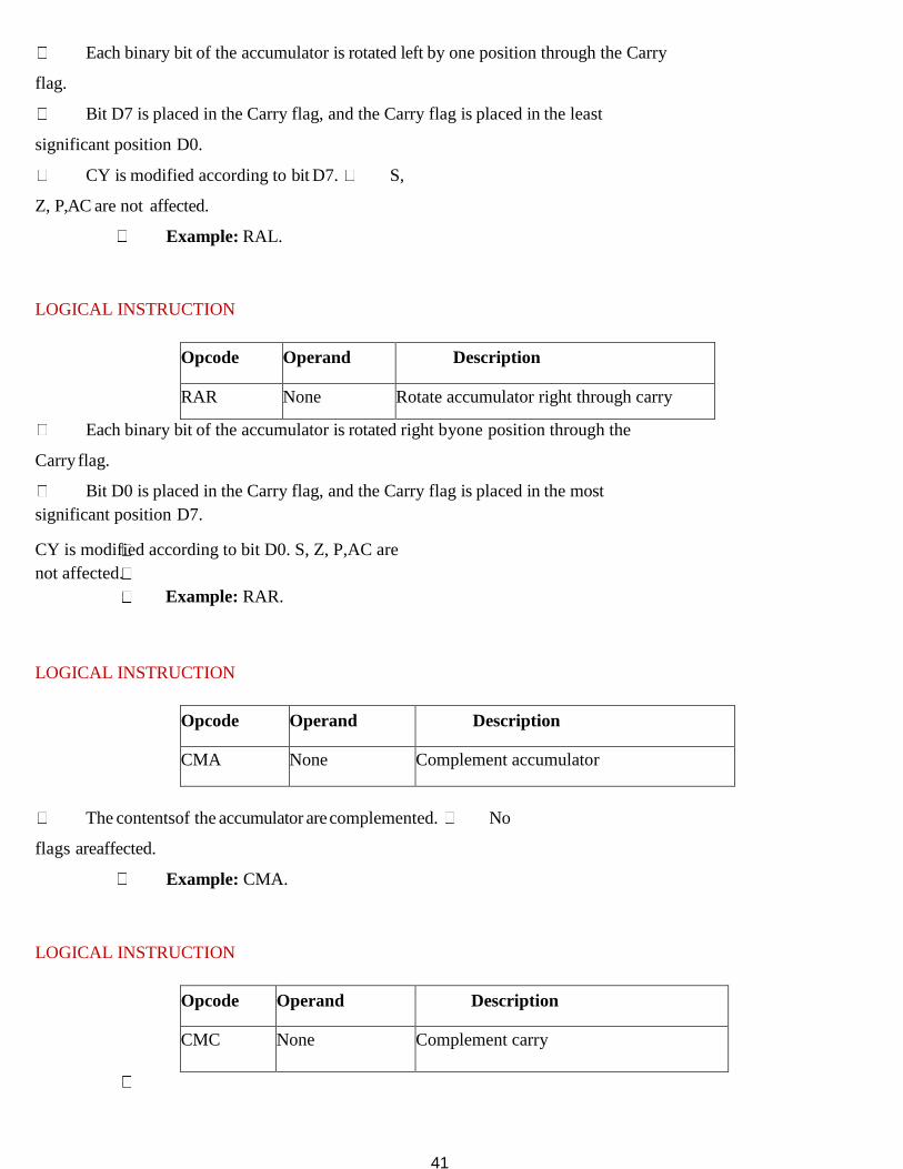
41
Each binary bit of the accumulator is rotated left by one position through the Carry
flag.
Bit D7 is placed in the Carry flag, and the Carry flag is placed in the least
significant position D0.
CY is modified according to bit D7. S,
Z, P,AC are not affected.
Example: RAL.
LOGICAL INSTRUCTION
Opcode Operand Description
RAR None Rotate accumulator right through carry
Each binary bit of the accumulator is rotated right byone position through the
Carry flag.
Bit D0 is placed in the Carry flag, and the Carry flag is placed in the most
significant position D7.
CY is modified according to bit D0. S, Z, P,AC are
not affected.
Example: RAR.
LOGICAL INSTRUCTION
Opcode Operand Description
CMA None Complement accumulator
The contentsof the accumulator are complemented. No
flags areaffected.
Example: CMA.
LOGICAL INSTRUCTION
Opcode Operand Description
CMC None Complement carry

42
The Carry flag iscomplemented. No
other flags areaffected.
Example: CMC.
LOGICAL INSTRUCTION
Opcode Operand Description
STC None Set carry
The Carry flag is set to1. No
other flags areaffected. Example:
STC.
BRANCH INSTRUCTIONS
The branching instruction alter the normal sequential flow. These
instructions alter either unconditionally or conditionally
BRANCH INSTRUCTIONS
Opcode Operand Description
JMP 16-bit address Jump unconditionally
The program sequence is transferred to thememory location specified by the 16-bit
address given in the operand.
Example: JMP 2034 H.
BRANCH INSTRUCTIONS
Opcode Operand Description
Jx 16-bit address Jump conditionally

43
The program sequence is transferred to thememory location specified by the 16-bit address
given in the operand based on the specified flag of thePSW.
Example: JZ 2034 H.
The program sequence is transferred to thememory location specified by the 16-bit
address given in the operand based on the specified flag of thePSW.
Before the transfer, the address of the next instruction after the call (the contents of the
program counter) is pushed onto thestack.
Example: CZ 2034 H.
JUMP CONDITIONALLY
Opcode Description Status Flags
JC Jump if Carry CY = 1
JNC Jump if No Carry CY = 0
JP Jump if Positive S = 0
JM Jump if Minus S = 1
JZ Jump if Zero Z = 1
JNZ Jump if No Zero Z = 0
JPE Jump if Parity Even P = 1
JPO Jump if Parity Odd P = 0
JUMP UNCONDITIONALLY
Opcode Operand Description
CALL 16-bit address Call unconditionally
44
The program sequence is transferred to thememory location specified
by the 16-bit address given in the operand.
Before the transfer, the address of the next instruction after CALL (the contents of the program
counter) is pushedonto the stack.
Example: CALL 2034 H.
RETURN UNCONDITIONALLY
Opcode Operand Description
RET None Return unconditionally
The program sequence is transferred fromthe subroutine to the
callingprogram.
The two bytes from the top of the stack are copied into the program counter, and program
execution beginsat the newaddress.
Example: RET.
RETURN CONDITIONALLY
Opcode Operand Description
Rx None Call conditionally
The program sequence is transferred from the subroutine to the calling program
based on the specified flag of the PSW.
The two bytes from the top of the stack are copied into the program counter, and program
execution beginsat the newaddress.
Example: RZ.
Opcode Description Status Flags
RC Return if Carry CY = 1
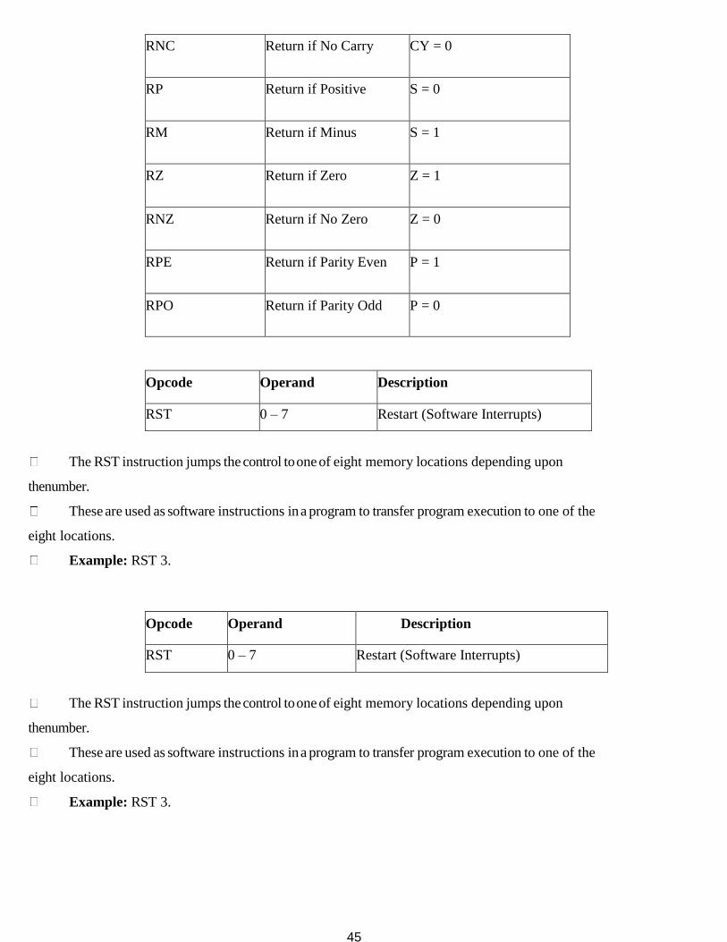
45
RNC Return if No Carry CY = 0
RP Return if Positive S = 0
RM Return if Minus S = 1
RZ Return if Zero Z = 1
RNZ Return if No Zero Z = 0
RPE Return if Parity Even P = 1
RPO Return if Parity Odd P = 0
Opcode Operand Description
RST 0 – 7 Restart (Software Interrupts)
The RST instruction jumps the control to one of eight memory locations depending upon
thenumber.
These are used as software instructions in a program to transfer program execution to one of the
eight locations.
Example: RST 3.
Opcode Operand Description
RST 0 – 7 Restart (Software Interrupts)
The RST instruction jumps the control to one of eight memory locations depending upon
thenumber.
These are used as software instructions in a program to transfer program execution to one of the
eight locations.
Example: RST 3.

46
RESRART ADDRESSES
Instructions Restart Address
RST 0 0000 H
RST 1 0008 H
RST 2 0010 H
RST 3 0018 H
RST 4 0020 H
RST 5 0028 H
RST 6 0030 H
RST 7 0038 H
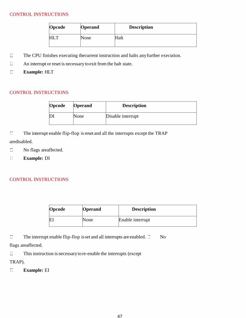
CONTROL INSTRUCTIONS
The control instructions control the operation of microprocessor.
Opcode Operand Description
NOP None No operation
No operation isperformed.
The instruction is fetched and decoded butno operation is executed.
Example: NOP
47
CONTROL INSTRUCTIONS
Opcode Operand Description
HLT None Halt
The CPU finishes executing thecurrent instruction and halts any further execution.
An interrupt or reset is necessary to exit from the halt state.
Example: HLT
CONTROL INSTRUCTIONS
Opcode Operand Description
DI None Disable interrupt
The interrupt enable flip-flop is reset and all the interrupts except the TRAP
aredisabled.
No flags areaffected.
Example: DI
CONTROL INSTRUCTIONS
Opcode Operand Description
EI None Enable interrupt
The interrupt enable flip-flop is set and all interrupts are enabled. No
flags areaffected.
This instruction is necessary to re-enable the interrupts (except
TRAP).
Example: EI
48
CONTROL INSTRUCTIONS
Opcode Operand Description
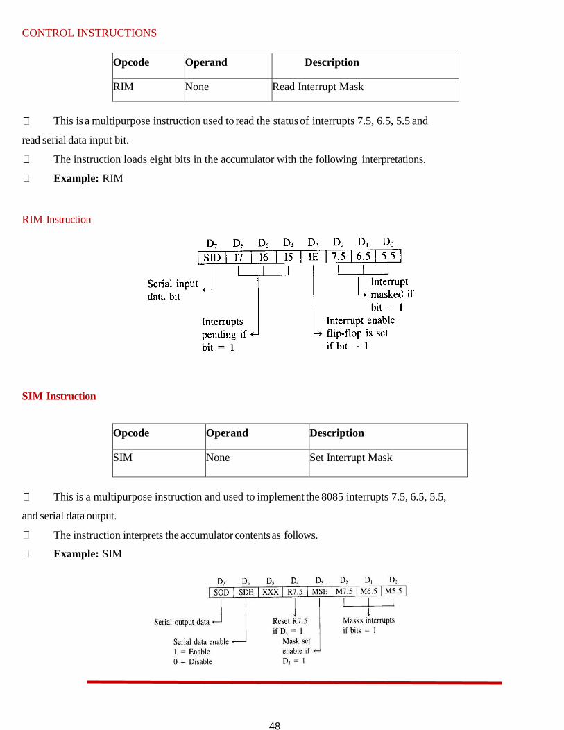
RIM None Read Interrupt Mask
This is a multipurpose instruction used to read the status of interrupts 7.5, 6.5, 5.5 and
read serial data input bit.
The instruction loads eight bits in the accumulator with the following interpretations.
Example: RIM
RIM Instruction
SIM Instruction
Opcode Operand Description
SIM None Set Interrupt Mask
This is a multipurpose instruction and used to implement the 8085 interrupts 7.5, 6.5, 5.5,
and serial data output.
The instruction interprets the accumulator contents as follows.
Example: SIM

49
ASSEMBLY LANGUAGE PROGRAMMING
1. Write a program to transfer a block of data from one location to the other.
5000 Start LXI B, 4A01
LXI H, 5101
MVI D,05
Loop MOV A, M
STAX B INX H
INX B
DCR D
JNZ
Loop HLT
2. Write an assembly language program to add two 8 bit umbers.
1) Start the program by loading the first data into Accumulator.
2) Move the data to a register (B register).
3) Get the second data and load into Accumulator.
4) Add the two register contents.
5) Check for carry.
6) Store the value of sum and carry in memorylocation.
7) Terminate the program.
MVI C, 00 Initialize C register to 00
LDA 4150 Load the value to Accumulator.
MVI C, 00 Initialize C register to 00
LDA 4150 Load the value to Accumulator.
MOV B, A Move the content of Accumulator to B register.
LDA 4151 Load the value to Accumulator.
ADD B Add the value of register B to A
JNC LOOP Jump on no carry.
INR C Increment value of register C
LOOP
: STA
4152 Store the value of Accumulator (SUM).
MOV A, C Move content of register C to Acc.
50
STA 4153 Store the value of Accumulator (CARRY)
HLT Halt the program.
3. Write an assembly language program to subtract two 8 bit numbers.
Start the program by loading the first data into Accumulator.
Move the data to a register (B register).
Get the second data and load into Accumulator.
Subtract the two register contents.
Check for carry.
If carry is present take 2’s complement of Accumulator.
Store the value of borrow in memory location.
Store the difference value (present in Accumulator) to amemory
location and terminate the program.
4.
5. JNC LOOP Jump on no carry.
6. CMA Complement Accumulator contents.
7. INR A Increment value in
Accumulator. INR C Increment value in register C
LOOP: STA 4152 Store the value of A-reg to memory address.
MOV A, C Move contents of register C to Accumulator.
4. STA 4153 Store the value of Accumulator memory address. 5. HLT Terminate the program. 6.
MVI C, 00 Initialize C to 00
LDA 4150 Load the value to Acc.
MOV B, A Move the content of Acc to B register.
LDA 4151 Load the value to Acc.
SUB B

51
3. Subtraction two 8-bit BCD number using 8085
1 Perform subtraction by tens complement method
2 Take nine’s complement of second no.( 99-no)
3 Add one to nine’s complement [(99-no) +1] to get 10’s complement
4 Add with first no.
5 Convert to BCD using DAA instr.
6 Store in memory location.
LDA 2050 H Load the first number to accumulator from
Memory
MOV B A Store the number in B reg.
LDA 2051H Load the second number to accumulator from
memory
MOV C A Store the number in C reg.
MVI A 99H Load acc. With 99H
SUB C Subtract second no from C reg.
ADD B Add the content with B reg.
DAA Convert to BCD using DAA instr.
STA 5052 Store in memory location.
HLT Halt the program.
4. Write an assembly language program to add two 16 bit numbers.
52
2050
2051
2060
2061
1. Clear the content in accumulator
2. Set the no. of bytes to be added in C reg.
3. Point to the first no.memory location by loading the address in HL reg. pair
4. Point to the second no.memory location by loading the address in DE reg. pair.
5. Add the first byte and store in first memory location
6. Decrement the counter reg. ; check for zero
6. Until zero continue adding
7. HLT
XRA A Clear the acc.
MVI C 02H Add 02H immediate data in C reg.
LXI H 2050H Load HL reg. pair with first memory location
LXI D
2060H
address
Load DE reg. pair with second memory location
address
HERE LDAX D load the content from memory whose address is
in DE reg. pair
ADC M Add with carry with the content in acc.
MOV M,A Copy the content from acc. to memory location
whose address is in HL reg.pair
INX H Increment the content in HL reg.pair
INX D ; Decrement the content in DE reg.pair DCR C;
Increment the content in C reg.
JNZ HERE : Continue the process from HERE; until zero
HLT Halt the program.
53
5. Write an assembly language program to subtract two 16 bit numbers.
1. Load the first no.from memory location to accumulator
2. Store it in B reg.
3. Load the second no.from memory
4. Subtract with first no.
5. Check for carry
6. If carry is produced; increment C reg.
7. Store the LSB and MSB to memory location.
LDA 2050 H Load the first no.from memory location to
accumulator
MOV B A Move the content from Acc. to B reg
LDA 2051H Load the second no.from memory location to
MVI C
OOH
accumulator
Clear C reg
SUB B Subtract the content from acc. with B reg
JNC GOTO Continue until Carry
INR C increment the content in C reg.
GOTO: STA
2052H
Store the content in acc. to memory (LSB)
MOV A C Copy the content from C.reg. to acc.(MSB
STA
2053H Store the content from acc. to memory
location(MSB)
HLT End program
6. Write an assembly language program to subtract two 8 bit BCD numbers.
LDA 2050 H MOV B,A LDA 2051H
MOV C,A MVI A,99H SUB C
INR A ADD B DAA
54
STA 2052H HLT
TEXT / REFERENCE BOOKS
1. Ramesh Goankar, "Microprocessor architecture programming and applications with 8085 / 8088", 5th
Edition, Penram International Publishing.
2. A.K.Ray and Bhurchandi, "Advanced Microprocessor", 1st Edition, TMH Publication.
3. Kenneth J.Ayala, "The 8051 microcontroller Architecture, Programming and applications" 2nd Edition
,Penram international.
4. Doughlas V.Hall, "Microprocessors and Digital system", 2nd Editon, Mc Graw Hill,1983.
5. Md.Rafiquzzaman, "Microprocessors and Microcomputer based system design", 2nd Editon,Universal Book
Stall, 1992.
6. Hardware Reference Manual for 80X86 family", Intel Corporation, 1990.
Question Bank
Part A
1. How many operations are there in the instruction set of 8085? 2. List out the five categories of the 8085 instructions. Give examples of the instructions for each group? 3. Explain the difference between a JMP instruction and CALL instruction 4. Explain the purpose of the I/O instructions IN and OUT. 5. What is the difference between the shifts and rotate instructions? 6. How many address lines in a 4096 x 8 EPROM CHIP? 7. What are the control signals used for DMA operation 8. What is meant by Wait State? 9. List the four instructions which control the interrupt structure of the 8085 microprocessor. 10. What is meant by interrupt?
Part B
1. A pharmacist is tasked with sorting and arranging ten drugs based on their MRP values in a cold storage unit. The drug which costs less should be placed at the last of the row and the drug with high MRP value should be placed at the top of the row. Assist the pharmacist by developing an Assembly language program using 8085 for the above said sorting application.
2. Examine the different Data Transfer instructions available in 8085 microprocessor in detail with necessary examples.
3. Interpret the use of different machine control instructions used in 8 bit 8085 processor.
4. Examine the use of different 8085 Logical instructions with necessary examples

UNIT- 3 INTERFACING
SECA1404- MICROPROCESSOR ANDMICROCONTROLLER BASED SYSTEMS
SCHOOL OF ELECTRICAL AND ELECTRONICS
DEPARTMENT OF ELECTRICAL AND ELECTRONICS ENGINEERING
55
III. INTERFACING
I. BASIC INTERFACE CONCEPTS
1. INTERFACING MEMORY AND I/O DEVICES WITH 8085
The programs and data that are executed by the microprocessor have to be
stored in ROM/EPROM and RAM, which are basically semiconductor
memory chips. The programs and data that are stored in ROM/EPROM are
not erased even when power supply to the chip is removed. Hence, they are
called non-volatile memory. They can be used to store permanent programs.
In a RAM, stored programs and data are erased when the power supply to the
chip is removed. Hence, RAM is called volatile memory. RAM can be used
to store programs and data that include, programs written during software
development for a microprocessor based system, program written when one
is learning assembly language programming and data enter while testing
these programs. In the memory-mapped I/O scheme, each I/O device is
assumed to be a memory location. Input and output devices, which are
interfaced with 8085, are essential in any microprocessor based system. They
can be interfaced using two schemes: I/O mapped I/O and memory-mapped
I/O. In the I/O mapped I/O scheme, the I/O devices are treated differently
from memory.
2. INTERFACING MEMORY CHIPS WITH 8085
8085 has 16 address lines (A0 - A15), hence a maximum of 64 KB (= 216
bytes) of memory locations can be interfaced with it. The memory address
space of the 8085 takes values from 0000H to FFFFH.
The 8085 initiates set of signals such as IO/M , RD and WR when it wants to
read from and write into memory. Similarly, each memory chip has signals
such as CE or CS (chip enable
or chip select), OE or RD (output enable or read) and WE or WR (write
enable or write) associated with it.
56
13 address lines of IC are connected to the corresponding address lines of
Operation
0 0 1 8085 reads data from memory
0 1 0 8085 writes data into memory
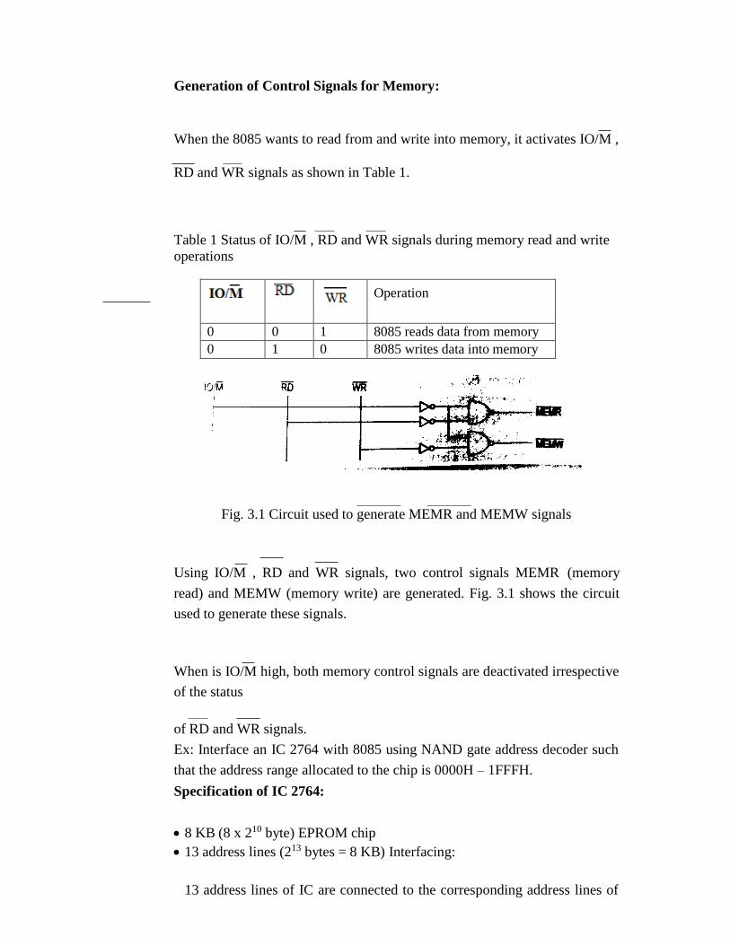
Generation of Control Signals for Memory:
When the 8085 wants to read from and write into memory, it activates IO/M ,
RD and WR signals as shown in Table 1.
Table 1 Status of IO/M , RD and WR signals during memory read and write
operations
Fig. 3.1 Circuit used to generate MEMR and MEMW signals
Using IO/M , RD and WR signals, two control signals MEMR (memory
read) and MEMW (memory write) are generated. Fig. 3.1 shows the circuit
used to generate these signals.
When is IO/M high, both memory control signals are deactivated irrespective
of the status
of RD and WR signals.
Ex: Interface an IC 2764 with 8085 using NAND gate address decoder such
that the address range allocated to the chip is 0000H – 1FFFH.
Specification of IC 2764:
8 KB (8 x 210 byte) EPROM chip
13 address lines (213 bytes = 8 KB) Interfacing:
57
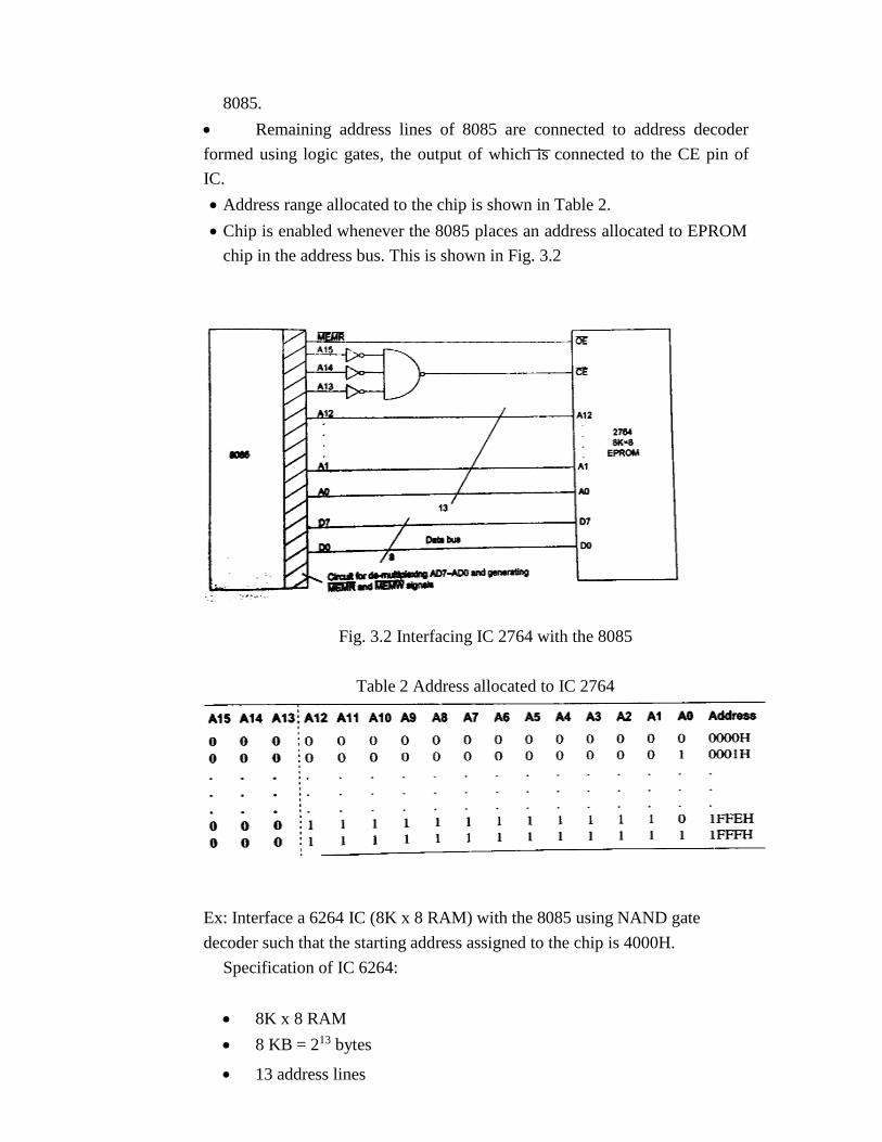
13 address lines
8085.
Remaining address lines of 8085 are connected to address decoder
formed using logic gates, the output of which is connected to the CE pin of
IC.
Address range allocated to the chip is shown in Table 2.
Chip is enabled whenever the 8085 places an address allocated to EPROM
chip in the address bus. This is shown in Fig. 3.2
Fig. 3.2 Interfacing IC 2764 with the 8085
Table 2 Address allocated to IC 2764
Ex: Interface a 6264 IC (8K x 8 RAM) with the 8085 using NAND gate
decoder such that the starting address assigned to the chip is 4000H.
Specification of IC 6264:
8K x 8 RAM
8 KB = 213 bytes
58
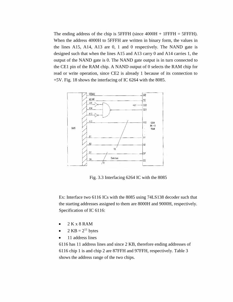
The ending address of the chip is 5FFFH (since 4000H + 1FFFH = 5FFFH).
When the address 4000H to 5FFFH are written in binary form, the values in
the lines A15, A14, A13 are 0, 1 and 0 respectively. The NAND gate is
designed such that when the lines A15 and A13 carry 0 and A14 carries 1, the
output of the NAND gate is 0. The NAND gate output is in turn connected to
the CE1 pin of the RAM chip. A NAND output of 0 selects the RAM chip for
read or write operation, since CE2 is already 1 because of its connection to
+5V. Fig. 18 shows the interfacing of IC 6264 with the 8085.
Fig. 3.3 Interfacing 6264 IC with the 8085
Ex: Interface two 6116 ICs with the 8085 using 74LS138 decoder such that
the starting addresses assigned to them are 8000H and 9000H, respectively.
Specification of IC 6116:
2 K x 8 RAM
2 KB = 211 bytes
11 address lines
6116 has 11 address lines and since 2 KB, therefore ending addresses of
6116 chip 1 is and chip 2 are 87FFH and 97FFH, respectively. Table 3
shows the address range of the two chips.
59
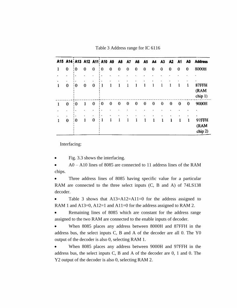
Table 3 Address range for IC 6116
Interfacing:
Fig. 3.3 shows the interfacing.
A0 – A10 lines of 8085 are connected to 11 address lines of the RAM
chips.
Three address lines of 8085 having specific value for a particular
RAM are connected to the three select inputs (C, B and A) of 74LS138
decoder.
Table 3 shows that A13=A12=A11=0 for the address assigned to
RAM 1 and A13=0, A12=1 and A11=0 for the address assigned to RAM 2.
Remaining lines of 8085 which are constant for the address range
assigned to the two RAM are connected to the enable inputs of decoder.
When 8085 places any address between 8000H and 87FFH in the
address bus, the select inputs C, B and A of the decoder are all 0. The Y0
output of the decoder is also 0, selecting RAM 1.
When 8085 places any address between 9000H and 97FFH in the
address bus, the select inputs C, B and A of the decoder are 0, 1 and 0. The
Y2 output of the decoder is also 0, selecting RAM 2.
60
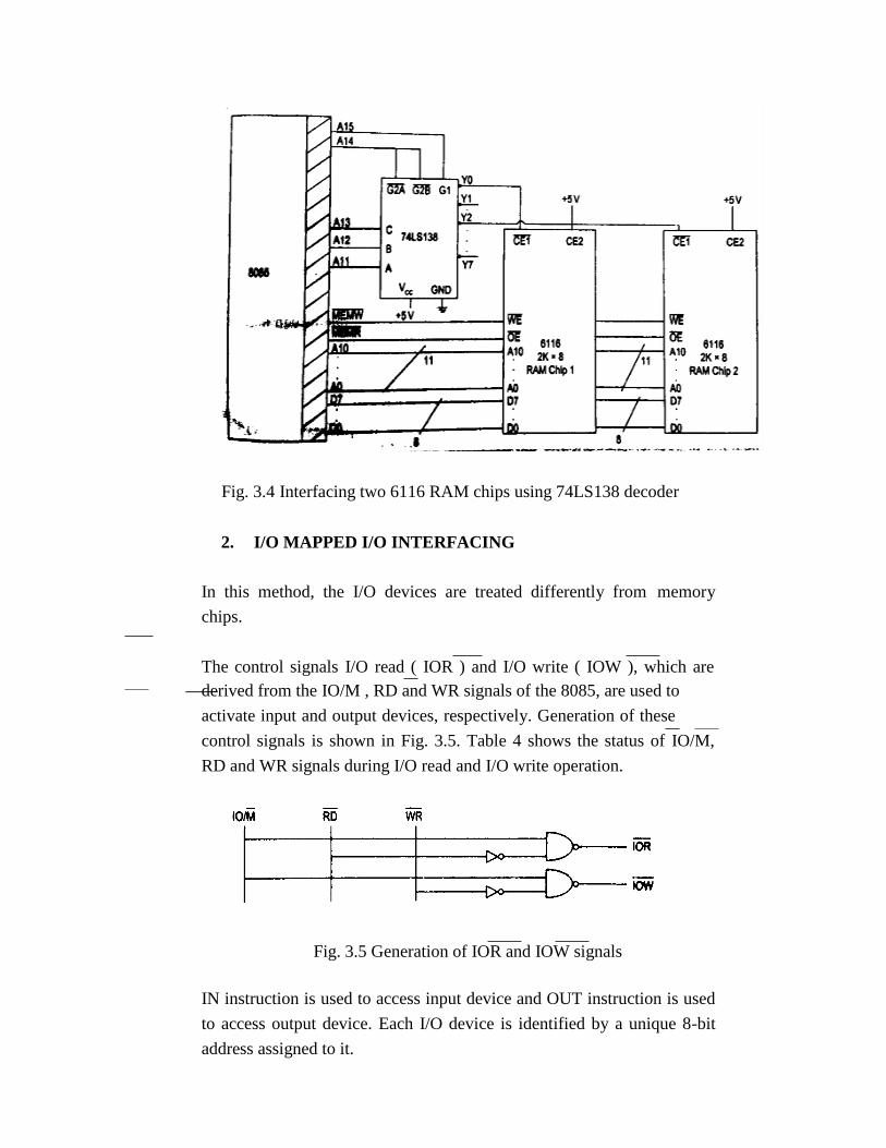
Fig. 3.4 Interfacing two 6116 RAM chips using 74LS138 decoder
2. I/O MAPPED I/O INTERFACING
In this method, the I/O devices are treated differently from memory
chips.
The control signals I/O read ( IOR ) and I/O write ( IOW ), which are
derived from the IO/M , RD and WR signals of the 8085, are used to
activate input and output devices, respectively. Generation of these
control signals is shown in Fig. 3.5. Table 4 shows the status of IO/M,
RD and WR signals during I/O read and I/O write operation.
Fig. 3.5 Generation of IOR and IOW signals
IN instruction is used to access input device and OUT instruction is used
to access output device. Each I/O device is identified by a unique 8-bit
address assigned to it.
61
Since the control signals used to access input and output devices are
different, and all I/O device use 8-bit address, a maximum of 256 (28)
input devices and 256 output devices can be interfaced with 8085.
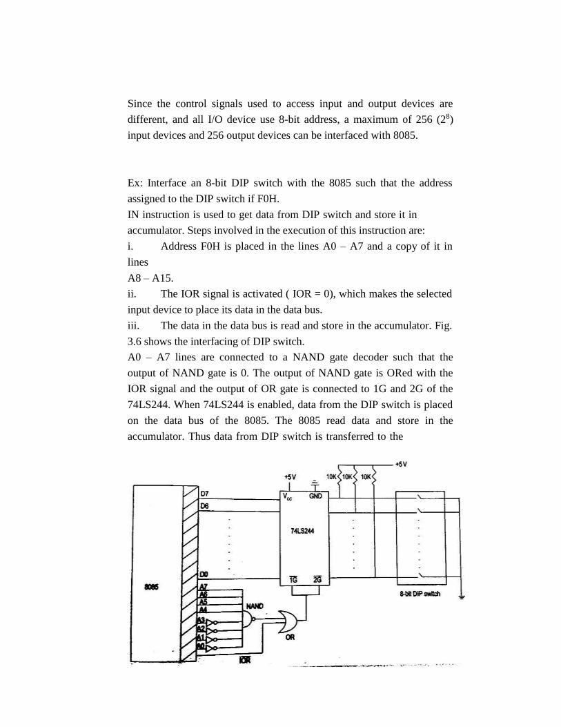
Ex: Interface an 8-bit DIP switch with the 8085 such that the address
assigned to the DIP switch if F0H.
IN instruction is used to get data from DIP switch and store it in
accumulator. Steps involved in the execution of this instruction are:
i. Address F0H is placed in the lines A0 – A7 and a copy of it in
lines
A8 – A15.
ii. The IOR signal is activated ( IOR = 0), which makes the selected
input device to place its data in the data bus.
iii. The data in the data bus is read and store in the accumulator. Fig.
3.6 shows the interfacing of DIP switch.
A0 – A7 lines are connected to a NAND gate decoder such that the
output of NAND gate is 0. The output of NAND gate is ORed with the
IOR signal and the output of OR gate is connected to 1G and 2G of the
74LS244. When 74LS244 is enabled, data from the DIP switch is placed
on the data bus of the 8085. The 8085 read data and store in the
accumulator. Thus data from DIP switch is transferred to the
62
accumulator.
Fig.3.6 Interfacing of 8-bit DIP switch with 8085
4. MEMORY MAPPED I/O INTERFACING
In memory-mapped I/O, each input or output device is treated as if it is a
memory location. The MEMR and MEMW control signals are used to
activate the devices. Each input or output device is identified by unique
16-bit address, similar to 16-bit address assigned to memory location. All
memory related instruction like LDA 2000H, LDAX B, MOV A, M can
be used.
Since the I/O devices use some of the memory address space of 8085, the
maximum memory capacity is lesser than 64 KB in this method.
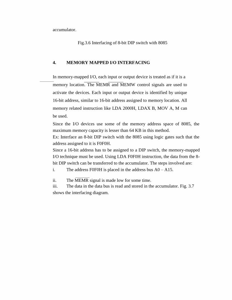
Ex: Interface an 8-bit DIP switch with the 8085 using logic gates such that the
address assigned to it is F0F0H.
Since a 16-bit address has to be assigned to a DIP switch, the memory-mapped
I/O technique must be used. Using LDA F0F0H instruction, the data from the 8-
bit DIP switch can be transferred to the accumulator. The steps involved are:
i. The address F0F0H is placed in the address bus A0 – A15.
ii. The MEMR signal is made low for some time.
iii. The data in the data bus is read and stored in the accumulator. Fig. 3.7
shows the interfacing diagram.
63
Fig. 3.7 Interfacing 8-bit DIP switch with 8085
When 8085 executes the instruction LDA F0F0H, it places the address
F0F0H in the address lines A0 – A15 as:
The address lines are connected to AND gates. The output of these gates
along with MEMR signal are connected to a NAND gate, so that when
the address F0F0H is placed in the address bus and MEMR = 0 its output
becomes 0, thereby enabling the buffer 74LS244. The data from the DIP
switch is placed in the 8085 data bus. The 8085 reads the data from the
data bus and stores it in the accumulator.
When 8085 executes the instruction LDA F0F0H, it places the address
F0F0H in the address lines A0 – A15 as:
The address lines are connected to AND gates. The output of these
gates along with MEMR
64
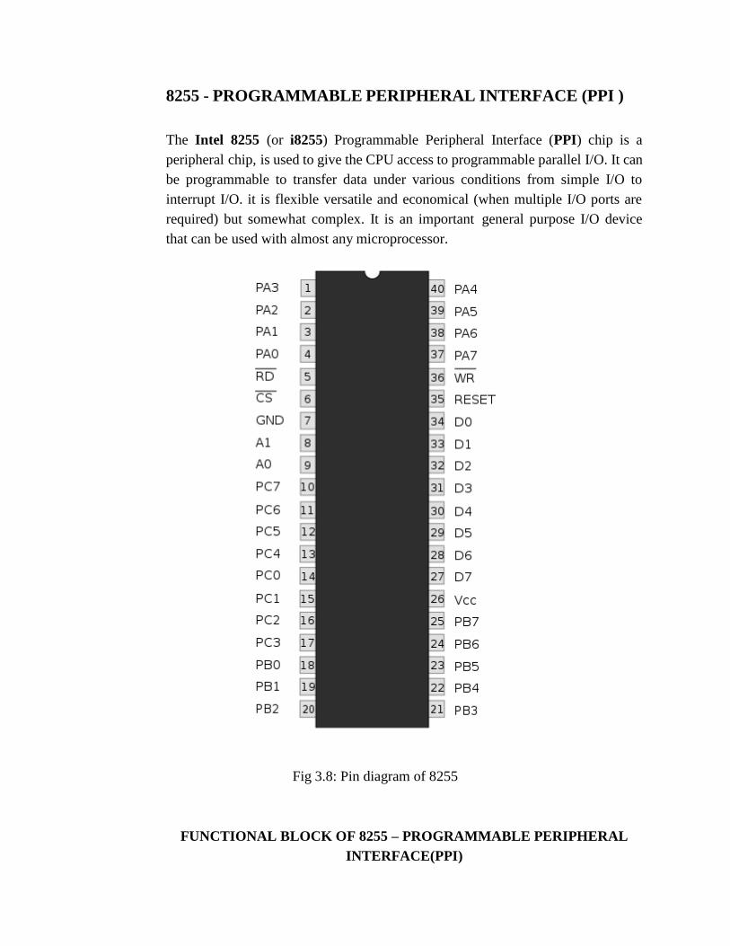
8255 - PROGRAMMABLE PERIPHERAL INTERFACE (PPI )
The Intel 8255 (or i8255) Programmable Peripheral Interface (PPI) chip is a
peripheral chip, is used to give the CPU access to programmable parallel I/O. It can
be programmable to transfer data under various conditions from simple I/O to
interrupt I/O. it is flexible versatile and economical (when multiple I/O ports are
required) but somewhat complex. It is an important general purpose I/O device
that can be used with almost any microprocessor.
Fig 3.8: Pin diagram of 8255
FUNCTIONAL BLOCK OF 8255 – PROGRAMMABLE PERIPHERAL
INTERFACE(PPI)
65
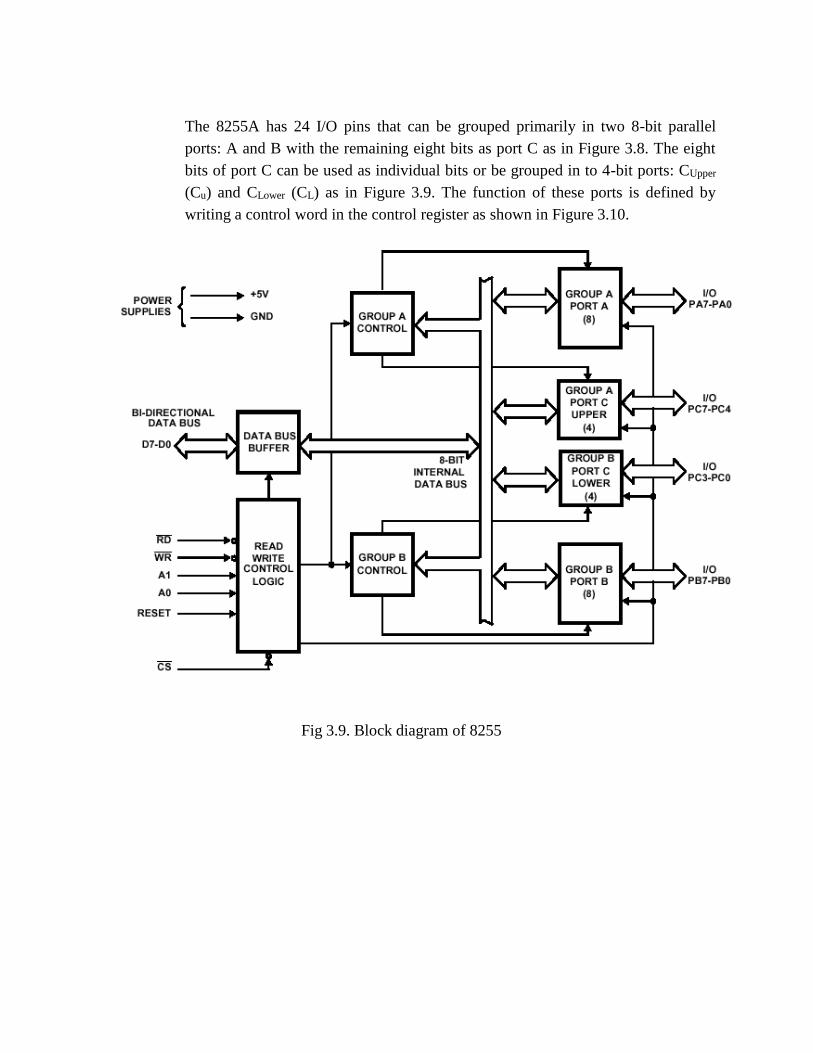
The 8255A has 24 I/O pins that can be grouped primarily in two 8-bit parallel
ports: A and B with the remaining eight bits as port C as in Figure 3.8. The eight
bits of port C can be used as individual bits or be grouped in to 4-bit ports: CUpper
(Cu) and CLower (CL) as in Figure 3.9. The function of these ports is defined by
writing a control word in the control register as shown in Figure 3.10.
Fig 3.9. Block diagram of 8255
66
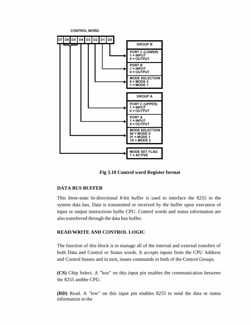
Fig 3.10 Control word Register format
DATA BUS BUFFER
This three-state bi-directional 8-bit buffer is used to interface the 8255 to the
system data bus. Data is transmitted or received by the buffer upon execution of
input or output instructions bythe CPU. Control words and status information are
also transferred through the data bus buffer.
READ/WRITE AND CONTROL LOGIC
The function of this block is to manage all of the internal and external transfers of
both Data and Control or Status words. It accepts inputs from the CPU Address
and Control busses and in turn, issues commands to both of the Control Groups.
(CS) Chip Select. A "low" on this input pin enables the communication between
the 8255 andthe CPU.
(RD) Read. A "low" on this input pin enables 8255 to send the data or status
information to the
67
CPU on the data bus. In essence, it allows the CPU to "read from" the 8255.
(WR) Write. A "low" on this input pin enables the CPU to write data or control
words into the8255.
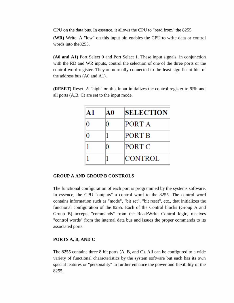
(A0 and A1) Port Select 0 and Port Select 1. These input signals, in conjunction
with the RD and WR inputs, control the selection of one of the three ports or the
control word register. Theyare normally connected to the least significant bits of
the address bus (A0 and A1).
(RESET) Reset. A "high" on this input initializes the control register to 9Bh and
all ports (A,B, C) are set to the input mode.
GROUP A AND GROUP B CONTROLS
The functional configuration of each port is programmed by the systems software.
In essence, the CPU "outputs" a control word to the 8255. The control word
contains information such as "mode", "bit set", "bit reset", etc., that initializes the
functional configuration of the 8255. Each of the Control blocks (Group A and
Group B) accepts "commands" from the Read/Write Control logic, receives
"control words" from the internal data bus and issues the proper commands to its
associated ports.
PORTS A, B, AND C
The 8255 contains three 8-bit ports (A, B, and C). All can be configured to a wide
variety of functional characteristics by the system software but each has its own
special features or "personality" to further enhance the power and flexibility of the
8255.
68
Port A One 8-bit data output latch/buffer and one 8-bit data input latch. Both
"pull-up" and "pull-down" bus-hold devices are present on Port A.
Port B One 8-bit data input/output latch/buffer and one 8-bit data input buffer.
Port C One 8-bit data output latch/buffer and one 8-bit data input buffer (no latch
for input). This port can be divided into two 4-bit ports under the mode control.
Each 4-bit port contains a 4-bit latch and it can be used for the control signal
output and status signal inputs in conjunction with ports A and B.
OPERATIONAL MODES OF 8255
There are two basic operational modes of 8255:
Bit set/reset Mode (BSR Mode).
Input/Output Mode (I/O Mode).
The two modes are selected on the basis of the value present at the D7 bit of the
Control WordRegister. When D7 = 1, 8255 operates in I/O mode and when D7 = 0,
it operates in the BSR mode.
1. BIT SET/RESET (BSR) MODE
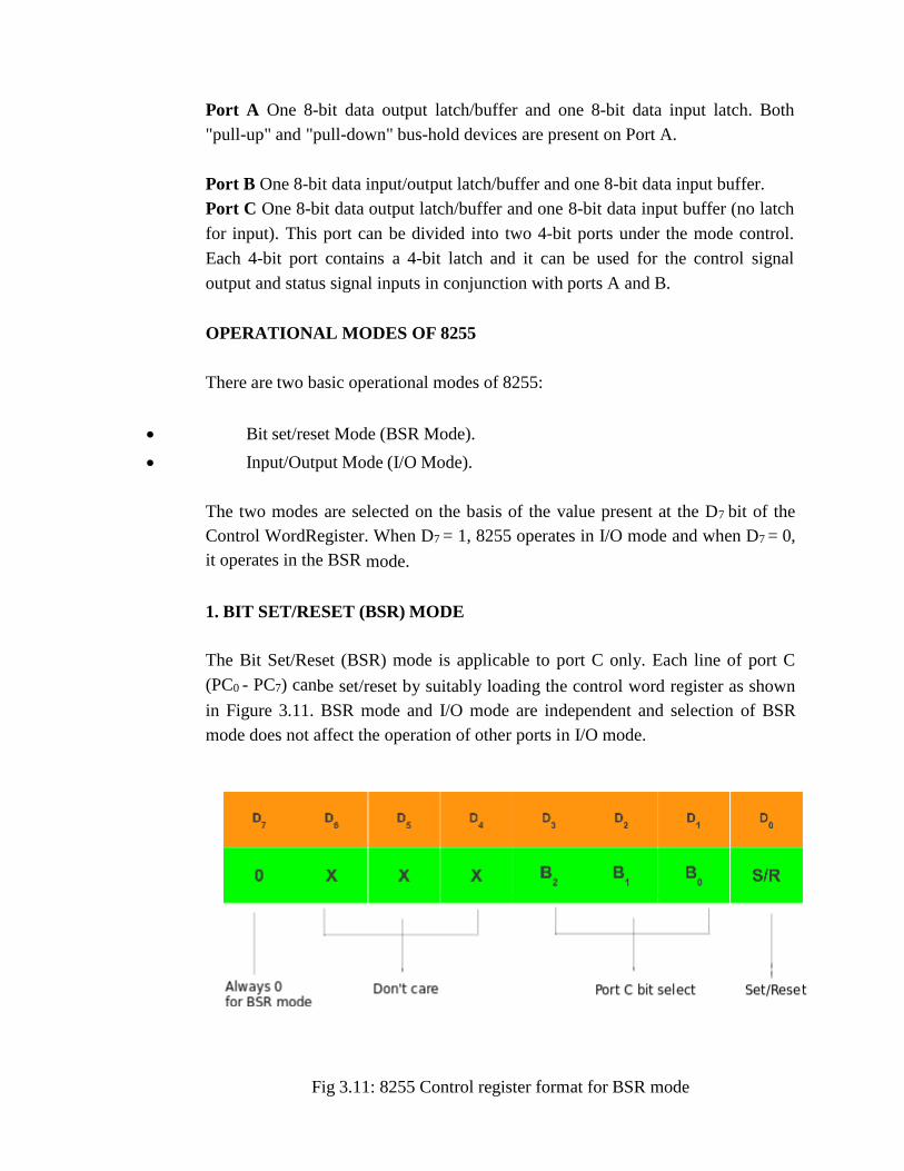
The Bit Set/Reset (BSR) mode is applicable to port C only. Each line of port C
(PC0 - PC7) canbe set/reset by suitably loading the control word register as shown
in Figure 3.11. BSR mode and I/O mode are independent and selection of BSR
mode does not affect the operation of other ports in I/O mode.
Fig 3.11: 8255 Control register format for BSR mode
69
D7 bit is always 0 for BSR mode.
Bits D6, D5 and D4 are don't care bits.
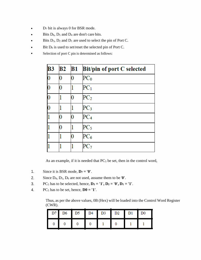
Bits D3, D2 and D1 are used to select the pin of Port C.
Bit D0 is used to set/reset the selected pin of Port C.
Selection of port C pin is determined as follows:
As an example, if it is needed that PC5 be set, then in the control word,
1. Since it is BSR mode, D7 = '0'.
2. Since D4, D5, D6 are not used, assume them to be '0'.
3. PC5 has to be selected, hence, D3 = '1', D2 = '0', D1 = '1'.
4. PC5 has to be set, hence, D0 = '1'.
Thus, as per the above values, 0B (Hex) will be loaded into the Control Word Register
(CWR).
70

2. INPUT/OUTPUT MODE
This mode is selected when D7 bit of the Control Word Register is 1. There are three I/O modes:
1. Mode 0 - Simple I/O
2. Mode 1 - Strobed I/O
3. Mode 2 - Strobed Bi-directional I/O
Figure 3.12: 8255 Control word for I/O mode
D0, D1, D3, D4 are assigned for lower port C, port B, upper port C and port A
respectively. When these bits are 1, the corresponding port acts as an input port.
For e.g., if D0 = D4 = 1, then lower port C and port A act as input ports. If these
bits are 0, then the corresponding port acts as an output port. For e.g., if D1 = D3
= 0, then port B and upper port C act as output ports as shown in Figure 3.12
D2 is used for mode selection of Group B (port B and lower port C). When D2 = 0,
mode 0 is selected and when D2 = 1, mode 1 is selected.
D5& D6 are used for mode selection of Group A ( port A and upper port C). The
selection is done as follows:
As it is I/O mode, D7 = 1.
71

For example, if port B and upper port C have to be initialized as input ports and
lower port C and port A as output ports (all in mode 0):
1. Since it is an I/O mode, D7 = 1.
2. Mode selection bits, D2, D5, D6 are all 0 for mode 0 operation.
3. Port B and upper port C should operate as Input ports, hence, D1 = D3 = 1.
4. Port A and lower port C should operate as Output ports, hence, D4 = D0 = 0.
Hence, for the desired operation, the control word register will have to be loaded with
"10001010" = 8A (hex).
Mode 0 - simple I/O
In this mode, the ports can be used for simple I/O operations without handshaking
signals. PortA, port B provide simple I/O operation. The two halves of port C can
be either used together as an additional 8-bit port, or they can be used as individual
4-bit ports. Since the two halves of port C are independent, they may be used such
that one- half is initialized as an input port while the other half is initialized as an
output port.
The input/output features in mode 0 are as follows:
1. Output ports are latched.
2. Input ports are buffered, not latched.
3. Ports do not have handshake or interrupt capability.
4. With 4 ports, 16 different combinations of I/O are possible.
Mode 0 – input mode
In the input mode, the 8255 gets data from the external peripheral ports and the
CPUreads the received data via its data bus.
The CPU first selects the
8255 chip by making CS low. Then it selects the
desired port using A0 and A1 lines.
The CPU then issues an RD signal to read the
data from the externalperipheral device via the system data bus.
72
Mode 0 - output mode
In the output mode, the CPU sends data to 8255 via system data bus and then the external
peripheral ports receive this data via 8255 port.
CPU first selects the 8255 chip by making CS low. It then selects the desired port
usingA0 and A1 lines.
CPU then issues a WR signal to write data to the selected port via the system
data bus. Thisdata is then received by the external peripheral device connected to
the selected port.
Mode 1
When we wish to use port A or port B for handshake (strobed) input or output
operation, we initialize that port in mode 1 (port A and port B can be initialized to
operate in different modes,i.e., for e.g., port A can operate in mode 0 and port B in
mode 1). Some of the pins of port C function as handshake lines.
For port B in this mode (irrespective of whether is acting as an input port or output
port), PC0,PC1 and PC2 pins function as handshake lines.
If port A is initialized as mode 1 input port, then, PC3, PC4 and PC5 function as
handshake signals. Pins PC6 and PC7 are available for use as input/output lines.
The mode 1 which supports handshaking has following
features:1.
Two ports i.e. port A and B can be used as 8-bit i/o ports.
2.
Each port uses three lines of port c as handshake signal and remaining two signals
canbe used as i/o ports.
3.
Interrupt logic is supported.
4.
Input and Output data are latched.
INPUT HANDSHAKING SIGNALS
1. IBF (Input Buffer Full) - It is an output indicating that the input latch contains
information.
73
2. STB (Strobed Input) - The strobe input loads data into the port latch, which holds
the information until it is input to the microprocessor via the IN instruction.
3. INTR (Interrupt request) - It is an output that requests an interrupt. The INTR pin
becomes a logic 1 when the STB input returns to a logic 1, and is cleared when the
data are input from the port by the microprocessor.
4. INTE (Interrupt enable) - It is neither an input nor an output; it is an internal bit
programmed via the port PC4 (port A) or PC2(port B) bit position.
OUTPUT HANDSHAKING SIGNALS
OBF (Output Buffer Full) - It is an output that goes low whenever data are
output(OUT) to the port A or port B latch. This signal is set to a logic 1 whenever
the ACK pulse returns from the external device.
ACK (Acknowledge)-It causes the OBF pin to return to a logic 1 level. The ACK
signal is a response from an external device, indicating that it has received the data
from the 82C55 port.
INTR (Interrupt request) - It is a signal that often interrupts the microprocessor
when the external device receives the data via the signal. this pin is qualified by
the internal INTE(interrupt enable) bit.
INTE (Interrupt enable) - It is neither an input nor an output; it is an internal bit
programmed to enable or disable the INTR pin. The INTE A bit is programmed
using the PC6 bit and INTE B is programmed using the PC2 bit.
Mode 2
Only group A can be initialized in this mode. Port A can be used for bidirectional
handshake data transfer. This means that data can be input or output on the same
eight lines (PA0 - PA7). Pins PC3 - PC7 are used as handshake lines for port A.
The remaining pins of port C (PC0 - PC2) can be used as input/output lines if
group B is initialized in mode 0 or as handshaking for port B if group B is
initialized in mode 1. In this mode, the 8255 may be used to extend the system bus
to a slave microprocessor or to transfer data bytes to and from a floppy disk
controller. Acknowledgement and handshaking signals are provided to maintain
proper data flow and synchronization between the data transmitter and receiver.
74
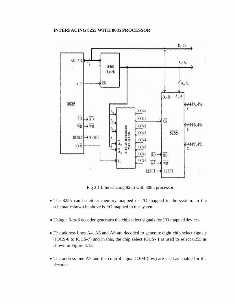
INTERFACING 8255 WITH 8085 PROCESSOR
Fig 3.13. Interfacing 8255 with 8085 processor
The 8255 can be either memory mapped or I/O mapped in the system. In the
schematicshown in above is I/O mapped in the system.
Using a 3-to-8 decoder generates the chip select signals for I/O mapped devices.
The address lines A4, A5 and A6 are decoded to generate eight chip select signals
(IOCS-0 to IOCS-7) and in this, the chip select IOCS- 1 is used to select 8255 as
shown in Figure 3.13.
The address line A7 and the control signal IO/M (low) are used as enable for the
decoder.
75
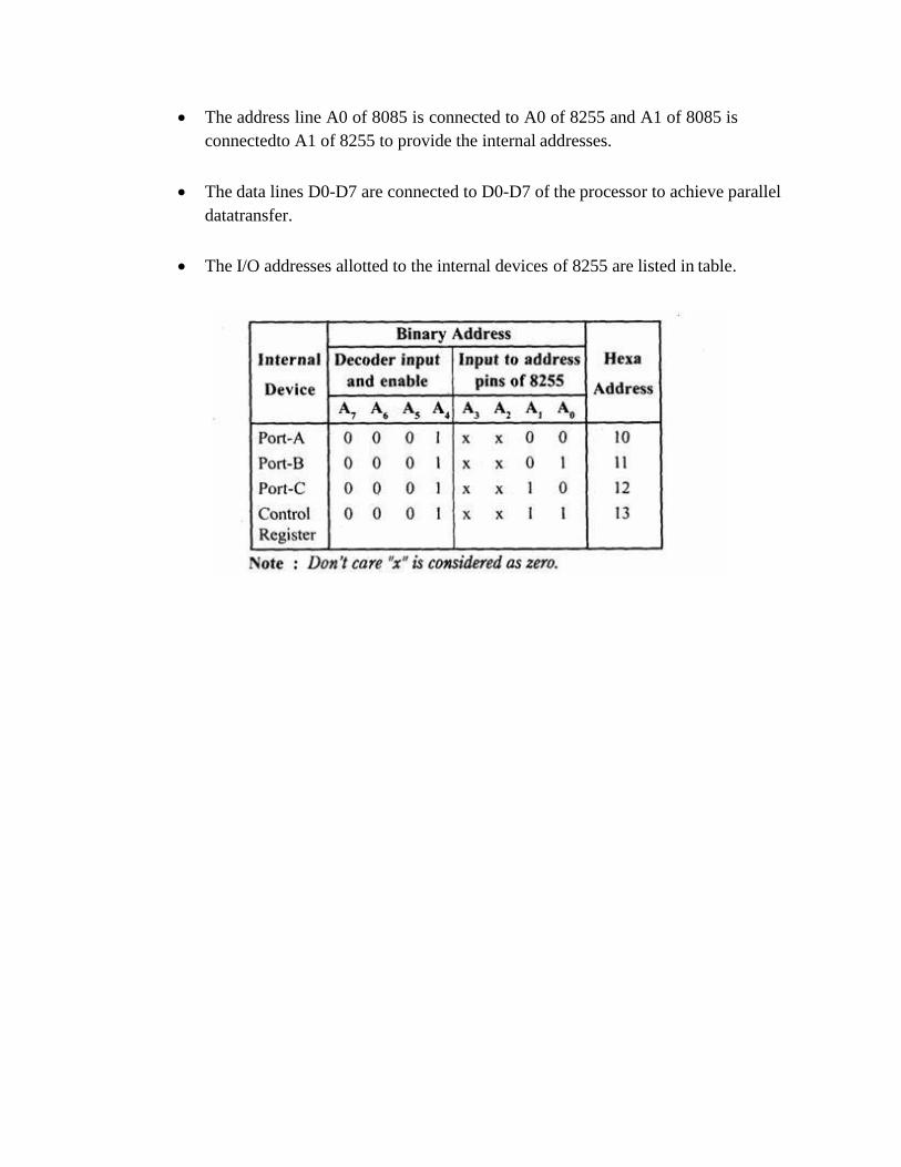
The address line A0 of 8085 is connected to A0 of 8255 and A1 of 8085 is
connectedto A1 of 8255 to provide the internal addresses.
The data lines D0-D7 are connected to D0-D7 of the processor to achieve parallel
datatransfer.
The I/O addresses allotted to the internal devices of 8255 are listed in table.
76
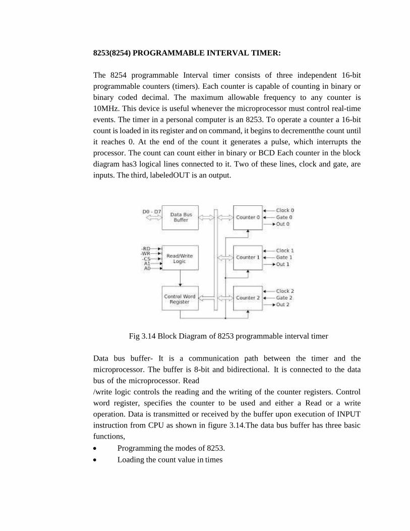
8253(8254) PROGRAMMABLE INTERVAL TIMER:
The 8254 programmable Interval timer consists of three independent 16-bit
programmable counters (timers). Each counter is capable of counting in binary or
binary coded decimal. The maximum allowable frequency to any counter is
10MHz. This device is useful whenever the microprocessor must control real-time
events. The timer in a personal computer is an 8253. To operate a counter a 16-bit
count is loaded in its register and on command, it begins to decrementthe count until
it reaches 0. At the end of the count it generates a pulse, which interrupts the
processor. The count can count either in binary or BCD Each counter in the block
diagram has3 logical lines connected to it. Two of these lines, clock and gate, are
inputs. The third, labeledOUT is an output.
Fig 3.14 Block Diagram of 8253 programmable interval timer
Data bus buffer- It is a communication path between the timer and the
microprocessor. The buffer is 8-bit and bidirectional. It is connected to the data
bus of the microprocessor. Read
/write logic controls the reading and the writing of the counter registers. Control
word register, specifies the counter to be used and either a Read or a write
operation. Data is transmitted or received by the buffer upon execution of INPUT
instruction from CPU as shown in figure 3.14.The data bus buffer has three basic
functions,
Programming the modes of 8253.
Loading the count value in times
77
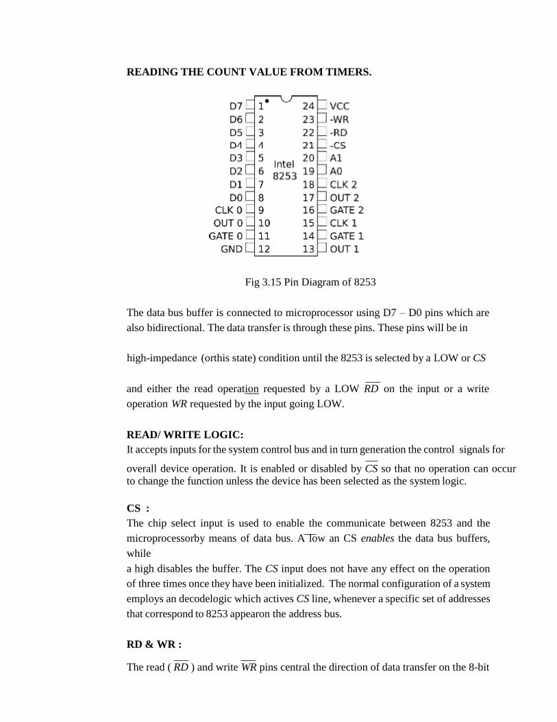
READING THE COUNT VALUE FROM TIMERS.
Fig 3.15 Pin Diagram of 8253
The data bus buffer is connected to microprocessor using D7 – D0 pins which are
also bidirectional. The data transfer is through these pins. These pins will be in
high-impedance (orthis state) condition until the 8253 is selected by a LOW or CS
and either the read operation requested by a LOW RD on the input or a write
operation WR requested by the input going LOW.
READ/ WRITE LOGIC:
It accepts inputs for the system control bus and in turn generation the control signals for
overall device operation. It is enabled or disabled by CS so that no operation can occur to change the function unless the device has been selected as the system logic.
CS :
The chip select input is used to enable the communicate between 8253 and the
microprocessorby means of data bus. A low an CS enables the data bus buffers,
while
a high disables the buffer. The CS input does not have any effect on the operation
of three times once they have been initialized. The normal configuration of a system
employs an decodelogic which actives CS line, whenever a specific set of addresses
that correspond to 8253 appearon the address bus.
RD & WR :
The read ( RD ) and write WR pins central the direction of data transfer on the 8-bit
78
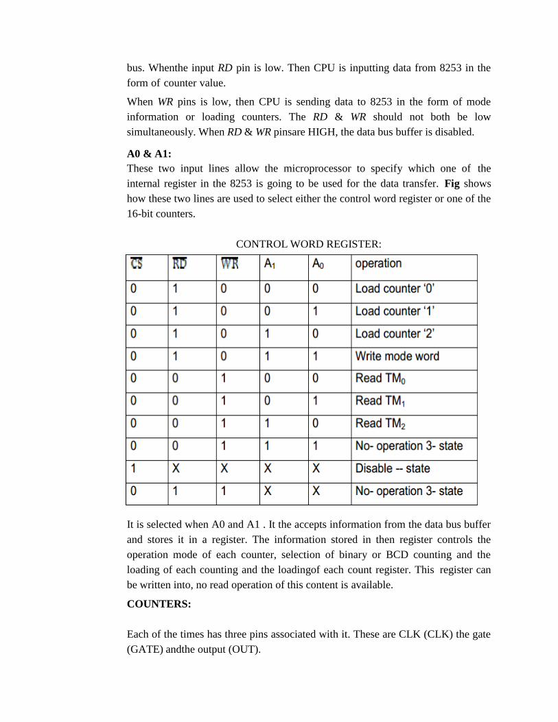
bus. Whenthe input RD pin is low. Then CPU is inputting data from 8253 in the
form of counter value.
When WR pins is low, then CPU is sending data to 8253 in the form of mode
information or loading counters. The RD & WR should not both be low
simultaneously. When RD & WR pinsare HIGH, the data bus buffer is disabled.
A0 & A1:
These two input lines allow the microprocessor to specify which one of the
internal register in the 8253 is going to be used for the data transfer. Fig shows
how these two lines are used to select either the control word register or one of the
16-bit counters.
CONTROL WORD REGISTER:
It is selected when A0 and A1 . It the accepts information from the data bus buffer
and stores it in a register. The information stored in then register controls the
operation mode of each counter, selection of binary or BCD counting and the
loading of each counting and the loadingof each count register. This register can
be written into, no read operation of this content is available.
COUNTERS:
Each of the times has three pins associated with it. These are CLK (CLK) the gate
(GATE) andthe output (OUT).
79
CLK:
This clock input pin provides 16-bit times with the signal to causes the times to
decrement maxm clock input is 2.6MHz. Note that the counters operate at the
negative edge (H1 to L0) ofthis clock input. If the signal on this pin is generated
by a fixed oscillator then the user has implemented a standard timer. If the input
signal is a string of randomly occurring pulses, thenit is called implementation of a
counter.
GATE:
The gate input pin is used to initiate or enable counting. The exact effect of the
gate signal depends on which of the six modes of operation is chosen.
OUTPUT:
The output pin provides an output from the timer. It actual use depends on the
mode of operation of the timer. The counter can be read ―in the fly‖ without
inhibiting gate pulse or clock input.
CONTROL REGISTER MODES OF OPERATION
Mode 0 Interrupt on terminal countMode 1 Programmable one shot Mode 2 Rate
Generator
Mode 3 Square wave rate GeneratorMode 4 Software triggered strobe Mode 5
Hardware triggered strobe
Mode 0: The output goes high after the terminal count is reached. The counter stops
if the Gateis low.. The timer count register is loaded with a count (say 6) when the
WR line is made lowby the processor. The counter unit starts counting down with
each clock pulse. The output goeshigh when the register value reaches zero. In the
mean time if the GATE is made low the countis suspended at the value(3) till the
GATE is enabled again .
80
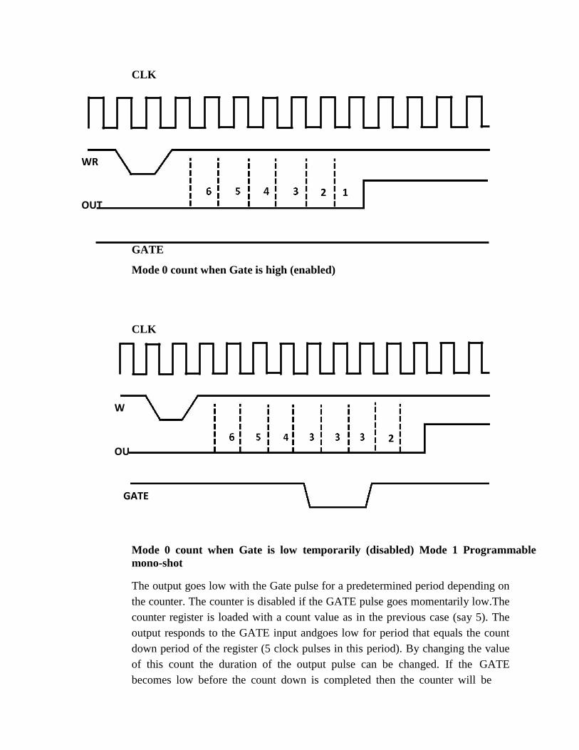
WR
2 1 OUT
W
2 OU
GATE
CLK
GATE
Mode 0 count when Gate is high (enabled)
CLK
Mode 0 count when Gate is low temporarily (disabled) Mode 1 Programmable
mono-shot
The output goes low with the Gate pulse for a predetermined period depending on
the counter. The counter is disabled if the GATE pulse goes momentarily low.The
counter register is loaded with a count value as in the previous case (say 5). The
output responds to the GATE input andgoes low for period that equals the count
down period of the register (5 clock pulses in this period). By changing the value
of this count the duration of the output pulse can be changed. If the GATE
becomes low before the count down is completed then the counter will be
81

GATE
5 4 3 2
OU
GATE (trigger)
suspended at that state as long as GATE is low. Thus it works as a mono-shot.
CLK
WR
Mode 1 The Gate goes high. The output goes low for the period depending
on the countCLK
WR
Mode 1 The Gate pulse is disabled momentarily causing the
counter to stop.Mode 2 Programmable Rate Generator
In this mode it operates as a rate generator. The output goes high for a period that
equals the
OUT
82
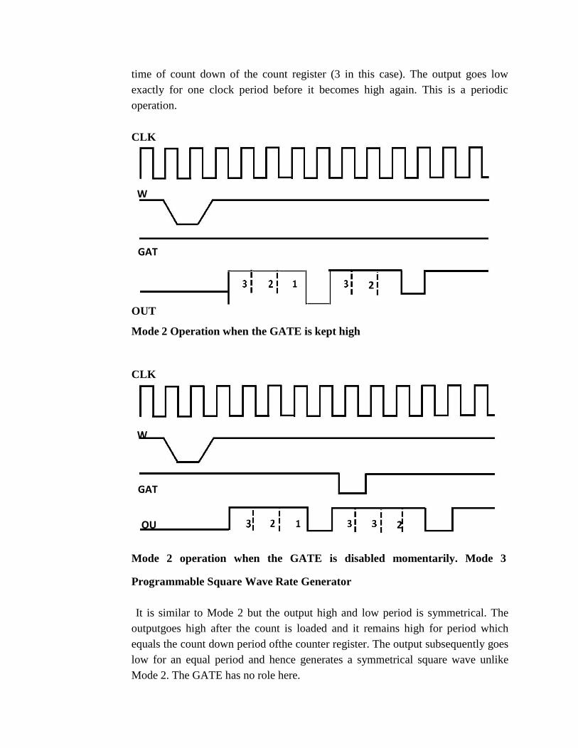
W
GAT
2
W
GAT
OU 2
time of count down of the count register (3 in this case). The output goes low
exactly for one clock period before it becomes high again. This is a periodic
operation.
CLK
OUT
Mode 2 Operation when the GATE is kept high
CLK
Mode 2 operation when the GATE is disabled momentarily. Mode 3
Programmable Square Wave Rate Generator
It is similar to Mode 2 but the output high and low period is symmetrical. The
outputgoes high after the count is loaded and it remains high for period which
equals the count down period ofthe counter register. The output subsequently goes
low for an equal period and hence generates a symmetrical square wave unlike
Mode 2. The GATE has no role here.
83
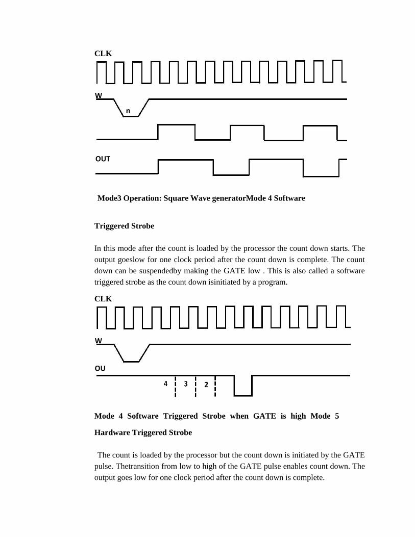
W
n
OUT
W
OU
2
CLK
Mode3 Operation: Square Wave generatorMode 4 Software
Triggered Strobe
In this mode after the count is loaded by the processor the count down starts. The
output goeslow for one clock period after the count down is complete. The count
down can be suspendedby making the GATE low . This is also called a software
triggered strobe as the count down isinitiated by a program.
CLK
Mode 4 Software Triggered Strobe when GATE is high Mode 5
Hardware Triggered Strobe
The count is loaded by the processor but the count down is initiated by the GATE
pulse. Thetransition from low to high of the GATE pulse enables count down. The
output goes low for one clock period after the count down is complete.
84
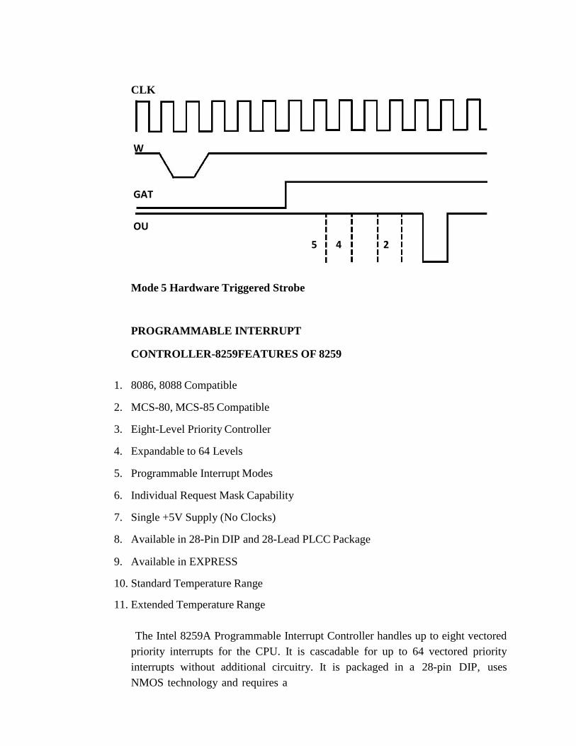
W
GAT
OU
5 4 2
CLK
Mode 5 Hardware Triggered Strobe
PROGRAMMABLE INTERRUPT
CONTROLLER-8259FEATURES OF 8259
1. 8086, 8088 Compatible
2. MCS-80, MCS-85 Compatible
3. Eight-Level Priority Controller
4. Expandable to 64 Levels
5. Programmable Interrupt Modes
6. Individual Request Mask Capability
7. Single +5V Supply (No Clocks)
8. Available in 28-Pin DIP and 28-Lead PLCC Package
9. Available in EXPRESS
10. Standard Temperature Range
11. Extended Temperature Range
The Intel 8259A Programmable Interrupt Controller handles up to eight vectored
priority interrupts for the CPU. It is cascadable for up to 64 vectored priority
interrupts without additional circuitry. It is packaged in a 28-pin DIP, uses
NMOS technology and requires a
85

single a5V supply. Circuitry is static, requiring no clock input. The 8259A is
designed to minimize the software and real time overhead in handling multi-level
priority interrupts. It has several modes, permitting optimization for a variety of
system requirements. The 8259A is fully upward compatible with the Intel 8259.
Software originally written for the 8259 will operate the 8259A in all 8259
equivalent modes (MCS-80/85, Non-Buffered, Edge Triggered). Pin Diagram of
8259 is shown in figure 17.
Fig.3.17 Pin Diagram of 8259
PIN DESCRIPTION OF 8259
86
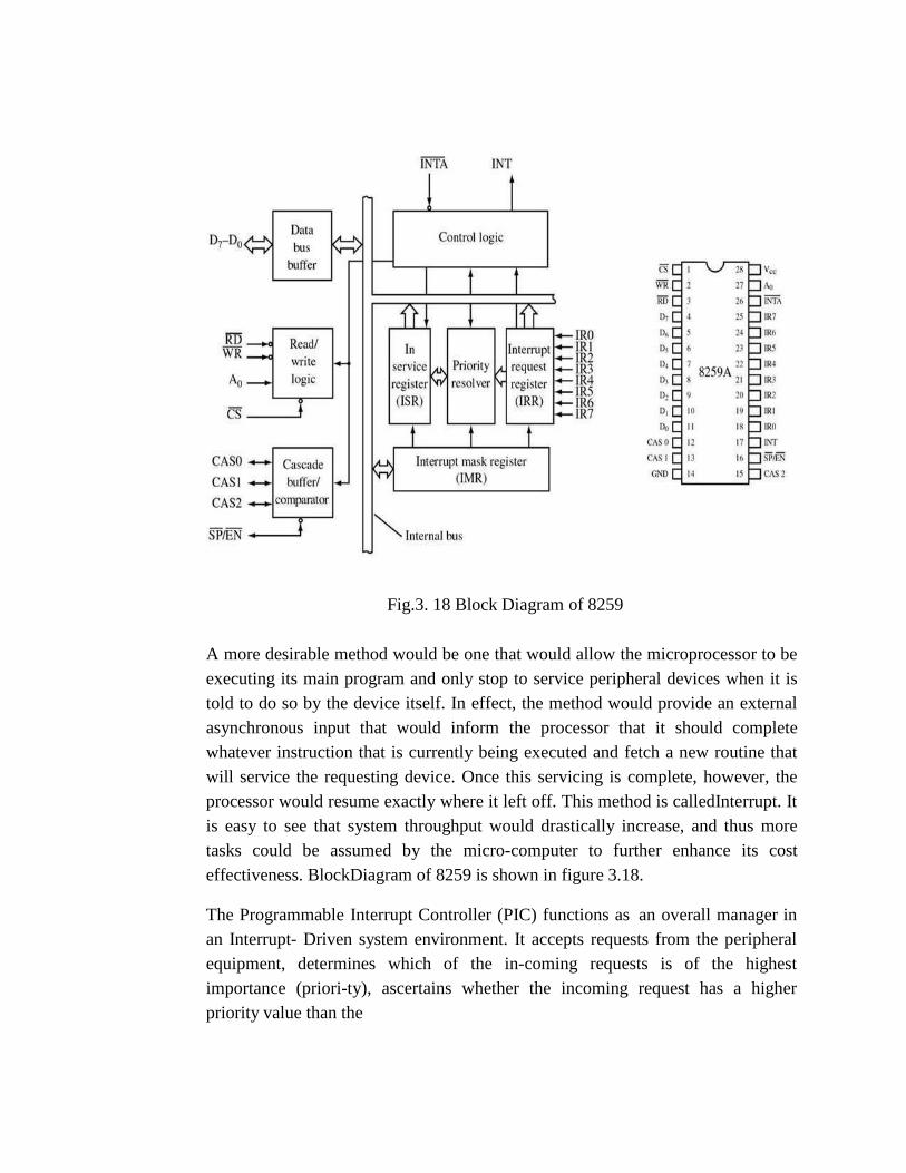
Fig.3. 18 Block Diagram of 8259
A more desirable method would be one that would allow the microprocessor to be
executing its main program and only stop to service peripheral devices when it is
told to do so by the device itself. In effect, the method would provide an external
asynchronous input that would inform the processor that it should complete
whatever instruction that is currently being executed and fetch a new routine that
will service the requesting device. Once this servicing is complete, however, the
processor would resume exactly where it left off. This method is calledInterrupt. It
is easy to see that system throughput would drastically increase, and thus more
tasks could be assumed by the micro-computer to further enhance its cost
effectiveness. BlockDiagram of 8259 is shown in figure 3.18.
The Programmable Interrupt Controller (PIC) functions as an overall manager in
an Interrupt- Driven system environment. It accepts requests from the peripheral
equipment, determines which of the in-coming requests is of the highest
importance (priori-ty), ascertains whether the incoming request has a higher
priority value than the
87

level currently being serviced, and issues an interrupt to the CPU based on this
determination.
The 8259A is a device specifically designed for use in real time, interrupt driven
microcomputer systems. It manages eight levels or requests and has built-in
features for expandability to other 8259A's (up to 64 levels). It is programmed by
the system's software as an I/O peripheral. A selection of priority modes is
available to the programmer so that the manner in which the requests are
processed by the 8259A can be configured to match his system requirements. The
priority modes can be changed or reconfigured dynamically at any time during the
main program. This means that the complete interrupt structure can be defined as
required, based on the total system environment.
INTERRUPT REQUEST REGISTER (IRR) AND IN-SERVICE REGISTER (ISR)
The interrupts at the IR input lines are handled by two registers in cascade, the
Interrupt Request Register (IRR) and the In-Service (ISR). The IRR is used to
store all the interrupt levels which are requesting service; and the ISR is used to
store all the interrupt levels which are being serviced.
PRIORITY RESOLVER
This logic block determines the priorites of the bits set in the IRR. The highest
priority is selected and strobed into the corresponding bit of the ISR during INTA
pulse.
INTERRUPT MASK REGISTER (IMR)
The IMR stores the bits which mask the interrupt lines to be masked. The IMR
operates on theIRR. Masking of a higher priority input will not affect the interrupt
request lines of lower quality.
INT (INTERRUPT)
This output goes directly to the CPU interrupt input. The VOH level on this line is
designed tobe fully compatible with the 8080A, 8085A and 8086 input levels.
88
INTA (INTERRUPT ACKNOWLEDGE)
INTA pulses will cause the 8259A to release vectoring information onto the data
bus. The format of this data depends on the system mode (mPM) of the 8259A.
DATA BUS BUFFER
This 3-state, bidirectional 8-bit buffer is used to inter-face the 8259A to the system
Data Bus. Control words and status information are transferred through the Data
Bus Buffer.
READ/WRITE CONTROL LOGIC
The function of this block is to accept Output commands from the CPU. It
contains the Initialization Command Word (ICW) registers and Operation
Command Word (OCW) registers which store the various control formats for
device operation. This function block also allows the status of the 8259A to be
transferred onto the Data Bus.
CS (CHIP SELECT)
A LOW on this input enables the 8259A. No reading or writing of the chip will
occur unless the device is selected.
WR (WRITE)
A LOW on this input enables the CPU to write con-trol words (ICWs and OCWs) to the
8259A.
RD (READ)
A LOW on this input enables the 8259A to send the status of the Interrupt Request
Register (IRR), In Service Register (ISR), the Interrupt Mask Register (IMR), or
the Interrupt level ontothe Data Bus.
A0
This input signal is used in conjunction with WR and RD signals to write
commands into the various command registers, as well as reading the various
status registers of the chip. This linecan be tied directly to one of the address lines.
89
INTERRUPT SEQUENCE
The powerful features of the 8259A in a microcomputer system are its
programmability and the interrupt routine addressing capability. The latter allows
direct or indirect jumping to the specific interrupt routine requested without any
polling of the interrupting devices. The normal sequence of events during an
interrupt depends on the type of CPU being used.
The events occur as follows in an MCS-80/85 sys-tem:
One or more of the INTERRUPT REQUEST lines (IR7±0) are raised high, setting
the correspond-ing IRR bit(s).
The 8259A evaluates these requests, and sends an INT to the CPU, if appropriate.
The CPU acknowledges the INT and responds with an INTA pulse.
Upon receiving an INTA from the CPU group, the highest priority ISR bit is set,
and the correspond-ing IRR bit is reset. The 8259A will also release a CALL
instruction code (11001101) onto the 8-bit Data Bus through its D7±0 pins.
This CALL instruction will initiate two more INTA pulses to be sent to the 8259A
from the CPU group.
These two INTA pulses allow the 8259A to re-lease its preprogrammed
subroutine address onto the Data Bus. The lower 8-bit address is released at the
first INTA pulse and the higher 8-bit address is released at the second INTA pulse.
This completes the 3-byte CALL instruction re-leased by the 8259A. In the AEOI
mode the ISR bit is reset at the end of the third INTA pulse. Otherwise, the ISR bit
remains set until an appropriate EOI command is issued at the end of the interrupt
sequence.
The events occurring in an 8086 system are the same until step 4.
Upon receiving an INTA from the CPU group, the highest priority ISR bit is set
and the corresponding IRR bit is reset. The 8259A does not drive the Data Bus
during this cycle.
The 8086 will initiate a second INTA pulse. During this pulse, the 8259A releases
an 8-bit pointer onto the Data Bus where it is read by the CPU.
This completes the interrupt cycle. In the AEOI mode the ISR bit is reset at the
end of the second INTA pulse. Otherwise, the ISR bit remains set until an
appropriate EOI command is issued at the end of the interrupt subroutine.
90
If no interrupt request is present at step 4 of either sequence (i.e., the request was
too short in duration) the 8259A will issue an interrupt level 7. Both the vectoring
bytes and the CAS lines will look like an interrupt level 7 was requested.
When the 8259A PIC receives an interrupt, INT be-comes active and an interrupt
acknowledgecycle is started. If a higher priority interrupt occurs between the two
INTA pulses, the INT linegoes inactive immediately after the second INTA pulse.
After an un- specified amount of timethe INT line is activated again to signify the
higher priority interrupt waiting for service. Thisinactive time is not specified and
can vary between parts. The designer should be aware of this consideration when
designing a sys-tem which uses the 8259A. It is recommended that proper
asynchronous design techniques be followed.
INITIALIZATION COMMAND WORDS
Whenever a command is issued with A0 e 0 and D4 e 1, this is interpreted as
Initialization Command Word 1 (ICW1). ICW1 starts the initialization sequence
during which the followingautomatically occur.
The edge sense circuit is reset, which means that following initialization, an
interruptrequest (IR) input must make a low-to-high transition to generate an
interrupt.
The Interrupt Mask Register is cleared.
IR7 input is assigned priority 7.
The slave mode address is set to 7.
Special Mask Mode is cleared and Status Read isset to IRR.
If IC4 e 0, then all functions selected in ICW4are set to zero. (Non-Buffered
mode(,noAuto-EOI, MCS-80, 85 system).
Initialization Command Word Format is as shown in figure 3.19.
91
92
Fig 3.19 . Initialization Command Word Format
93
OPERATION COMMAND WORDS
After the Initialization Command Words (ICWs) are programmed into the 8259A,
the chip is ready to accept interrupt requests at its input lines. However, during the
8259A operation, a selection of algorithms can command the 8259A to operate in
various modes through the Operation Command Words (OCWs). Operation
Command Word format is as shown in figure20
Fig . Operational Control Words
94

Fig 3.20 Operation Command Word Format
DMA CONTROLLER 8257
The Direct Memory Access or DMA mode of data transfer is the fastest amongstall
the modes of data transfer. In this mode, the device may transfer data directly
to/from memory without any interference from the CPU. The device requests the
CPU (through aDMA controller) to hold its data, address and control bus, so that
the device may transfer data directly to/from memory. The DMA data transfer is
initiated only after receiving HLDA signal from the CPU. Intel’s 8257 is a four
channel DMA controller designed to be interfaced with their family of
microprocessors. The 8257, on behalf of the devices, requests the CPU for bus
access using local bus request input i.e. HOLD in minimum mode. In maximum
mode of the microprocessor RQ/GT pin is used as bus request input. On receiving
the HLDA signal (in minimum mode) orRQ/GT signal (in maximum mode) from
the CPU, the requesting devices gets the access of the bus, and it completes the
required number of DMA cycles for the data transfer and then hands over the
control of the bus back to the CPU.
INTERNAL ARCHITECTURE OF 8257
The internal architecture of 8257 is shown in figure. The chip support four DMA
channels, i.e. four peripheral devices can independently request for DMA data
transfer
95
through these channels at a time. The DMA controller has 8-bit internal data buffer,
a read/write unit, a control unit, a priority resolving unit along with a set of
registers.
The 8257 performs the DMA operation over four independent DMA channels.
Each of four channels of 8257 has a pair of two 16-bit registers, viz. DMA address
register and terminal count register.
There are two common registers for all the channels, namely, mode set register
and status register. Thus there are a total of ten registers. The CPU selects one of
these ten registers using address lines Ao-A3. Table shows how the Ao-A3 bits
may be used for selecting one of theseregisters.
DMA ADDRESS REGISTER
Each DMA channel has one DMA address register. The function of this register is
to store theaddress of the starting memory location, which will be accessed by the
DMA channel. Thus the starting address of the memory block which will be
accessed by the device is first loaded in the DMA address register of the channel.
The device that wants to transfer data over a DMAchannel, will access the block of
the memory with the starting address stored in the DMA Address Register.
TERMINAL COUNT REGISTER
Each of the four DMA channels of 8257 has one terminal count register (TC). This
16-bit register is used for ascertaining that the data transfer through a DMA
channel ceases or stops after the required number of DMA cycles. The low order
14-bits of the terminal count register are initialized with the binary equivalent of
the number of required DMA cycles minus one. After each DMA cycle, the
terminal count register content will be decremented by one and finally it becomes
zero after the required number of DMA cycles are over. The bits14 and 15 of this
register indicate the type of the DMA operation (transfer). If the device wants to
write data into the memory, the DMA operation is called DMA write operation. Bit
14 of the registerin this case will be set to one and bit 15 will be set to zero.
96
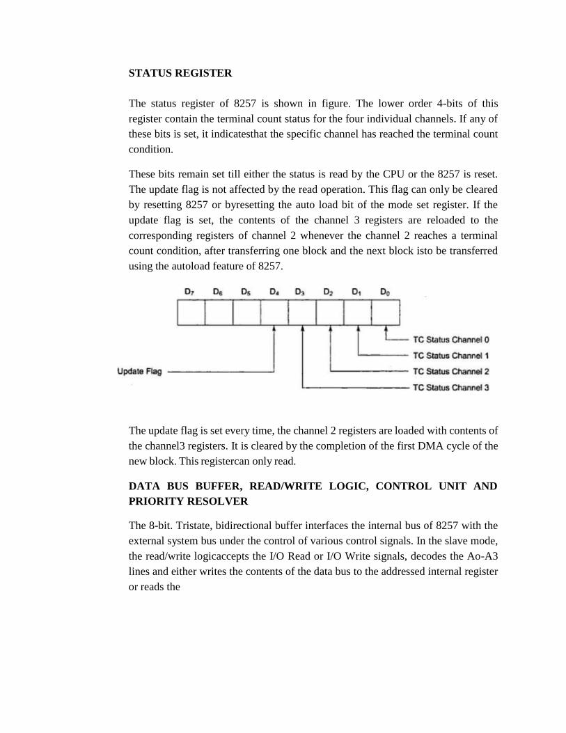
STATUS REGISTER
The status register of 8257 is shown in figure. The lower order 4-bits of this
register contain the terminal count status for the four individual channels. If any of
these bits is set, it indicatesthat the specific channel has reached the terminal count
condition.
These bits remain set till either the status is read by the CPU or the 8257 is reset.
The update flag is not affected by the read operation. This flag can only be cleared
by resetting 8257 or byresetting the auto load bit of the mode set register. If the
update flag is set, the contents of the channel 3 registers are reloaded to the
corresponding registers of channel 2 whenever the channel 2 reaches a terminal
count condition, after transferring one block and the next block isto be transferred
using the autoload feature of 8257.
The update flag is set every time, the channel 2 registers are loaded with contents of
the channel3 registers. It is cleared by the completion of the first DMA cycle of the
new block. This registercan only read.
DATA BUS BUFFER, READ/WRITE LOGIC, CONTROL UNIT AND
PRIORITY RESOLVER
The 8-bit. Tristate, bidirectional buffer interfaces the internal bus of 8257 with the
external system bus under the control of various control signals. In the slave mode,
the read/write logicaccepts the I/O Read or I/O Write signals, decodes the Ao-A3
lines and either writes the contents of the data bus to the addressed internal register
or reads the
97
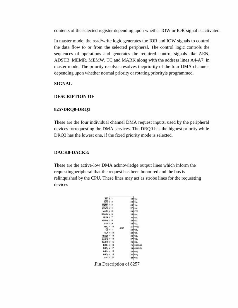
contents of the selected register depending upon whether IOW or IOR signal is activated.
In master mode, the read/write logic generates the IOR and IOW signals to control
the data flow to or from the selected peripheral. The control logic controls the
sequences of operations and generates the required control signals like AEN,
ADSTB, MEMR, MEMW, TC and MARK along with the address lines A4-A7, in
master mode. The priority resolver resolves thepriority of the four DMA channels
depending upon whether normal priority or rotating priorityis programmed.
SIGNAL
DESCRIPTION OF
8257DRQ0-DRQ3
These are the four individual channel DMA request inputs, used by the peripheral
devices forrequesting the DMA services. The DRQ0 has the highest priority while
DRQ3 has the lowest one, if the fixed priority mode is selected.
DACK0-DACK3:
These are the active-low DMA acknowledge output lines which inform the
requestingperipheral that the request has been honoured and the bus is
relinquished by the CPU. These lines may act as strobe lines for the requesting
devices
.Pin Description of 8257
98
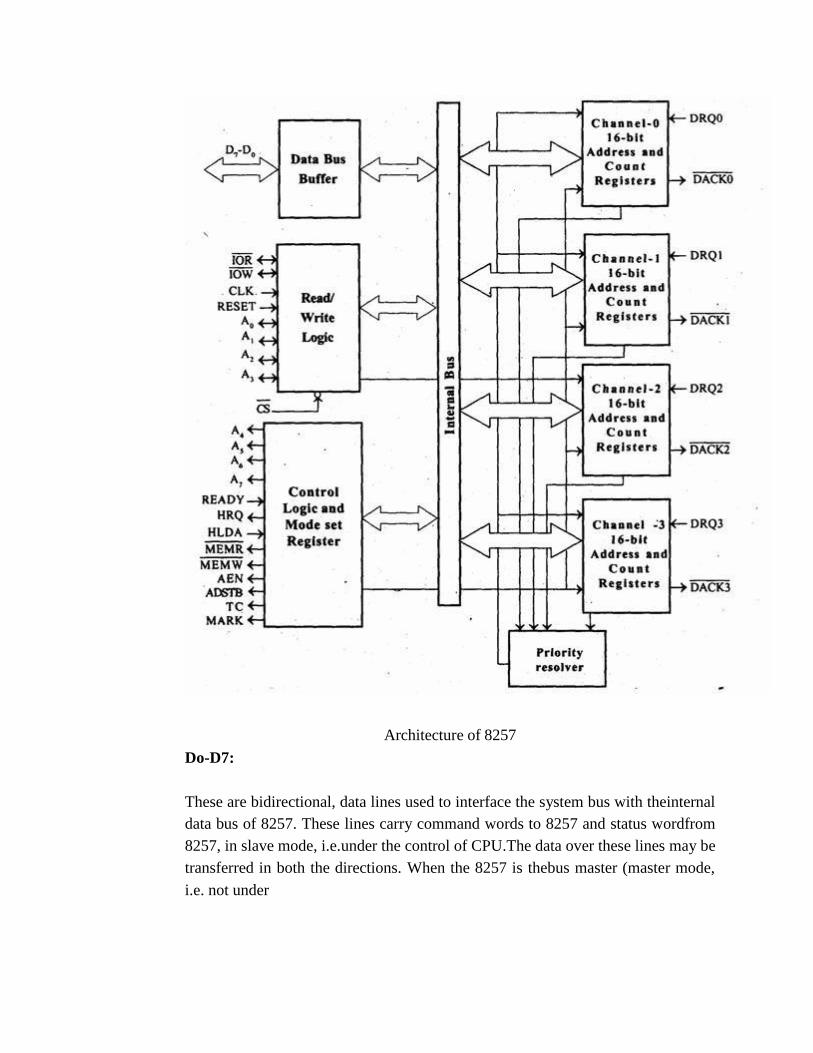
Architecture of 8257
Do-D7:
These are bidirectional, data lines used to interface the system bus with theinternal
data bus of 8257. These lines carry command words to 8257 and status wordfrom
8257, in slave mode, i.e.under the control of CPU.The data over these lines may be
transferred in both the directions. When the 8257 is thebus master (master mode,
i.e. not under
99
CPU control), it uses Do-D7 lines to send higherbyte of the generated address to the
latch. Thisaddress is further latched using ADSTBsignal. the address is transferred
over Do-D7 during the first clock cycle of the DMAcycle. During the rest of the
period, data is available on the data bus.
IOR:
This is an active-low bidirectional tristate input line that acts as an input in
theslave mode. In slave mode, this input signal is used by the CPU to read internal
registersof 8257.this line actsoutput in master mode. In master mode, this signal is
used to readdata from a peripheral duringa memory write cycle.
IOW:
This is an active low bidirection tristate line that acts as input in slave mode to
load the contents of the data bus to the 8-bit mode register or upper/lower byte of a
16-bit DMA addressregister or terminal count register. In the master mode, it is a
control output that loads the datato a peripheral during DMA memory read cycle
(write to peripheral).
CLK:
This is a clock frequency input required to derive basic system timings for
theinternal operationof 8257.
RESET :
This active-high asynchronous input disables all the DMA channels by clearing
the mode register and tristates all the control lines.
Ao-A3:
These are the four least significant address lines. In slave mode, they act as input
which selectone of the registers to be read or written. In the master mode, they are
the four least significantmemory address output lines generated by 8257.
100

CS:
This is an active-low chip select line that enables the read/write operations
from/to 8257, in slave mode. In the master mode, it is automatically disabled to
prevent the chip from getting selected (by CPU) while performing the DMA
operation.
A4-A7:
This is the higher nibble of the lower byte address generated by 8257 during the
master modeof DMA operation.
READY:
This is an active-high asynchronous input used to stretch memory read and
writecycles of 8257 by inserting wait states. This is used while interfacing slower
peripherals.
HRQ:
The hold request output requests the access of the system bus. In the
noncascaded8257 systems,this is connected with HOLD pin of CPU. In the cascade
mode, this pin of a slave is connectedwith a DRQ input line of the master 8257,
while that of the master is connected with HOLD input of the CPU.
HLDA :
The CPU drives this input to the DMA controller high, while granting the bus
tothe device. This pin is connected to the HLDA output of the CPU. This input, if
high, indicates to the DMA controller that the bus has been granted to the
requesting peripheral by the CPU.
MEMR:
This active –low memory read output is used to read data from the addressed
memory locationsduring DMA read cycles.
MEMW :
This active-low three state output is used to write data to the addressed memory
location duringDMA write operation.
101
ADST :
This output from 8257 strobes the higher byte of the memory address generated by
the DMA controller into the latches.
AEN:
This output is used to disable the system data bus and the control the bus driven by
the CPU, this may be used to disable the system address and data bus by using the
enable input of the bus drivers to inhibit the non-DMA devices from responding
during DMA operations. If the 8257 is I/O mapped, this should be used to disable
the other I/O devices, when the DMA controller addresses is on the address bus.
TC:
Terminal count output indicates to the currently selected peripherals that thepresent
DMA cycleis the last for the previously programmed data block. If the TC STOP bit
in the mode set registeris set, the selected channel will be disabled at the end of the
DMA cycle. The TC pin is activatedwhen the 14-bit content of the terminal count
register of the selected channel becomes equal tozero. The lower order 14 bits of
the terminal count register are to be programmed with a 14-bitequivalent of (n-1),
if n is the desired number of DMA cycles.
MARK:
The modulo 128 mark output indicates to the selected peripheral that the current
DMA cycle is the 128th cycle since the previous MARK output. The mark will be
activated after each 128cycles or integral multiples of it from the beginning if the
data block (the first DMA cycle), ifthe total number of the required DMA cycles
(n) is completely divisible by 128.
Vcc:
This is a +5v supply pin required for operation of the circuit. GND:This is a return
line for the supply (ground pin of the IC).
102

REFERENCE BOOKS
1. Ramesh Gaonkar, “Microprocessor Architecture, Programming and
applications with8085”, 5th Edition, Penram International Publishing Pvt Ltd,
2010.
2. D. V. Hall, “Microprocessor Interfacing, Programming and
Hardware”, McGraw Hill,1993.
3. Nagoor Kani A, “Microprocessor (8085) and its Applications”, 2nd
Edition, RBApublications.
4. Mathur A.P, “Introduction to Microprocessor”, Tata McGraw Hill, 1990.
PART – A QUESTIONS
S.NO QUESTION
1 What is memory?
2 What is interfacing?
3 What Is the need of 8255?
4 What is the need of 8253?
5 What is the need of 8259?
6 What is the need of 8257?
7 What Is Chip Select? How It Is Generated?
8 What are the different types of semiconductor memory?
9 What is SRAM and DRAM
10 List the characteristics of SRAM and DRAM?
PART – B QUESTIONS
S.NO QUESTION
1 Describe the operation and applications of 8257 with neat diagrams.
2 Explain the initialization sequence of 8259.
3 Write about the command words of 8259 and explain briefly about 8259.
4 Draw and explain the functional block diagram of programmable peripheral interface (8255). Write about the command words of 8255.
5 Draw and explain the functional block diagram of programmable counter/interval timer (8254). Write about the command words of 8253.
103

SCHOOL OF COMPUTING
DEPARTMENT OF COMPUTER SCIENCE ENGINEERING
UNIT – IV – 8086 Architecture – SECA1404
104
8086 Microprocessor is an enhanced version of 8085Microprocessor that was designed by
Intel in 1976. It is a 16-bit Microprocessor having 20 address lines and16 data lines that
provides up to 1MB storage. It consists of powerful instruction set, which provides
operations like multiplication and division easily.
It supports two modes of operation, i.e. Maximum mode and Minimum mode. Maximum
mode is suitable for system having multiple processors and Minimum mode is suitable for
system having a single processor.
Features of 8086 The most prominent features of a 8086 microprocessor are as follows −
• It has an instruction queue, which is capable of storing six instruction bytes from the memory
resulting in faster processing.
• It was the first 16-bit processor having 16-bit ALU, 16-bit registers, internal data bus, and 16-bit
external data bus resulting in faster processing.
• It is available in 3 versions based on the frequency of operation −
o 8086 → 5MHz
o 8086-2 → 8MHz
o (c)8086-1 → 10 MHz
• It uses two stages of pipelining, i.e. Fetch Stage and Execute Stage, which improves
performance.
• Fetch stage can prefetch up to 6 bytes of instructions and stores them in the queue.
• Execute stage executes these instructions.
• It has 256 vectored interrupts.
• It consists of 29,000 transistors.
Comparison between 8085 & 8086 Microprocessor
105
• Size − 8085 is 8-bit microprocessor, whereas 8086 is 16-bit microprocessor.
• Address Bus − 8085 has 16-bit address bus while 8086 has 20-bit address bus.
• Memory − 8085 can access up to 64Kb, whereas 8086 can access up to 1 Mb of memory.
• Instruction − 8085 doesn’t have an instruction queue, whereas 8086 has an instruction queue.
• Pipelining − 8085 doesn’t support a pipelined architecture while 8086 supports a pipelined
architecture.
• I/O − 8085 can address 2^8 = 256 I/O's, whereas 8086 can access 2^16 = 65,536 I/O's.
• Cost − The cost of 8085 is low whereas that of 8086 is high.
Architecture of 8086 The following diagram depicts the architecture of a 8086 Microprocessor
−
8086 Microprocessor is divided into two functional units, i.e., EU (Execution
Unit) and BIU (Bus Interface Unit).
EU (Execution Unit) Execution unit gives instructions to BIU stating from where to fetch the data and then
decode and execute those instructions. Its function is to control operations on data using
the instruction decoder & ALU. EU has no direct connection with system buses as shown in
the above figure, it performs operations over data through BIU.
Let us now discuss the functional parts of 8086 microprocessors.
ALU
It handles all arithmetic and logical operations, like +, −, ×, /, OR, AND, NOT operations.
106
Flag Register
It is a 16-bit register that behaves like a flip-flop, i.e. it changes its status according to the
result stored in the accumulator. It has 9 flags and they are divided into 2 groups −
Conditional Flags and Control Flags.
Conditional Flags
It represents the result of the last arithmetic or logical instruction executed. Following is
the list of conditional flags −
• Carry flag − This flag indicates an overflow condition for arithmetic operations.
• Auxiliary flag − When an operation is performed at ALU, it results in a carry/barrow from lower
nibble (i.e. D0 – D3) to upper nibble (i.e. D4 – D7), then this flag is set, i.e. carry given by D3 bit
to D4 is AF flag. The processor uses this flag to perform binary to BCD conversion.
• Parity flag − This flag is used to indicate the parity of the result, i.e. when the lower order 8-bits
of the result contains even number of 1’s, then the Parity Flag is set. For odd number of 1’s, the
Parity Flag is reset.
• Zero flag − This flag is set to 1 when the result of arithmetic or logical operation is zero else it is
set to 0.
• Sign flag − This flag holds the sign of the result, i.e. when the result of the operation is negative,
then the sign flag is set to 1 else set to 0.
• Overflow flag − This flag represents the result when the system capacity is exceeded.
Control Flags
Control flags controls the operations of the execution unit. Following is the list of control
flags −
• Trap flag − It is used for single step control and allows the user to execute one instruction at a
time for debugging. If it is set, then the program can be run in a single step mode.
• Interrupt flag − It is an interrupt enable/disable flag, i.e. used to allow/prohibit the interruption
of a program. It is set to 1 for interrupt enabled condition and set to 0 for interrupt disabled
condition.
107
• Direction flag − It is used in string operation. As the name suggests when it is set then string
bytes are accessed from the higher memory address to the lower memory address and vice-a-
versa.
General purpose register
There are 8 general purpose registers, i.e., AH, AL, BH, BL, CH, CL, DH, and DL. These
registers can be used individually to store 8-bit data and can be used in pairs to store 16bit
data. The valid register pairs are AH and AL, BH and BL, CH and CL, and DH and DL. It is
referred to the AX, BX, CX, and DX respectively.
• AX register − It is also known as accumulator register. It is used to store operands for arithmetic
operations.
• BX register − It is used as a base register. It is used to store the starting base address of the
memory area within the data segment.
• CX register − It is referred to as counter. It is used in loop instruction to store the loop counter.
• DX register − This register is used to hold I/O port address for I/O instruction.
Stack pointer register
It is a 16-bit register, which holds the address from the start of the segment to the memory
location, where a word was most recently stored on the stack.
BIU (Bus Interface Unit) BIU takes care of all data and addresses transfers on the buses for the EU like sending
addresses, fetching instructions from the memory, reading data from the ports and the
memory as well as writing data to the ports and the memory. EU has no direction
connection with System Buses so this is possible with the BIU. EU and BIU are connected
with the Internal Bus.
It has the following functional parts −
• Instruction queue − BIU contains the instruction queue. BIU gets upto 6 bytes of next
instructions and stores them in the instruction queue. When EU
108

executes instructions and is ready for its next instruction, then it simply reads the instruction
from this instruction queue resulting in increased execution speed.
• Fetching the next instruction while the current instruction executes is called pipelining.
• Segment register − BIU has 4 segment buses, i.e. CS, DS, SS& ES. It holds the addresses of
instructions and data in memory, which are used by the processor to access memory locations.
It also contains 1 pointer register IP, which holds the address of the next instruction to executed
by the EU.
o CS − It stands for Code Segment. It is used for addressing a memory location in the code
segment of the memory, where the executable program is stored.
o DS − It stands for Data Segment. It consists of data used by the program andis accessed
in the data segment by an offset address or the content of other register that holds the
offset address.
o SS − It stands for Stack Segment. It handles memory to store data and addresses during
execution.
o ES − It stands for Extra Segment. ES is additional data segment, which is used by the
string to hold the extra destination data.
• Instruction pointer − It is a 16-bit register used to hold the address of the next instruction to be
executed.
8086 Microprocessor is divided into two functional units,
i.e., EU (Execution Unit) and BIU (Bus Interface Unit).
The Bus Interface Unit (BIU) generates the 20-bit physical memory address and provides the interface with external memory (ROM/RAM). As mentioned earlier, 8086 has a single memory interface. To speed up the execution, 6- bytes of instruction are fetched in advance and kept in a 6-byte Instruction Queue while other instructions are being executed in the Execution Unit (EU). Hence after the execution of an instruction, the next instruction is directly fetched from the instruction queue without having to wait for the external memory to send the instruction. This is called pipe-lining and is helpful for speeding up the overall execution process.
8086's BIU produces the 20-bit physical memory address by combining a 16- bit segment address with a 16-bit offset address. There are four 16-bit
109
segment registers, viz., the code segment (CS), the stack segment (SS), the extra segment (ES), and the data segment (DS). These segment registers hold the corresponding 16-bit segment addresses. A segment address is the upper 16-bits of the starting address of that segment. The lower 4-bits of the starting address of a segment is always zero. The offset address is held by another 16-bit register. The physical 20-bit address is calculated by shifting the segment address 4-bit left and then adding that to the offset address.
For Example:
Code segment Register CS holds the segment address which is 4569 H Instruction pointer IP holds the offset address which is 10A0 H The physical 20-bit address is calculated as follows.
Segment address: 45690 H Offset address :+ 10A0 H Physical address : 46730 H
EU (Execution Unit) Execution unit gives instructions to BIU stating from where to fetch the data and then
decode and execute those instructions. Its function is to control operations on data using
the instruction decoder & ALU. EU has no direct connection with system buses as shown in
the above figure, it performs operations over data through BIU.
Let us now discuss the functional parts of 8086 microprocessors.
ALU
It handles all arithmetic and logical operations, like +, −, ×, /, OR, AND, NOT operations.
Flag Register
It is a 16-bit register that behaves like a flip-flop, i.e. it changes its status according to the
result stored in the accumulator. It has 9 flags and they are divided into 2 groups −
Conditional Flags and Control Flags.
Conditional Flags
It represents the result of the last arithmetic or logical instruction executed. Following is
the list of conditional flags −
• Carry flag − This flag indicates an overflow condition for arithmetic operations.
110
• Auxiliary flag − When an operation is performed at ALU, it results in a carry/barrow from lower
nibble (i.e. D0 – D3) to upper nibble (i.e. D4 – D7), then this flag is set, i.e. carry given by D3 bit
to D4 is AF flag. The processor uses this flag to perform binary to BCD conversion.
• Parity flag − This flag is used to indicate the parity of the result, i.e. when the lower order 8-bits
of the result contains even number of 1’s, then the Parity Flag is set. For odd number of 1’s, the
Parity Flag is reset.
• Zero flag − This flag is set to 1 when the result of arithmetic or logical operation is zero else it is
set to 0.
• Sign flag − This flag holds the sign of the result, i.e. when the result of the operation is negative,
then the sign flag is set to 1 else set to 0.
• Overflow flag − This flag represents the result when the system capacity is exceeded.
Control Flags
Control flags controls the operations of the execution unit. Following is the list of control
flags −
• Trap flag − It is used for single step control and allows the user to execute one instruction at a
time for debugging. If it is set, then the program can be run in a single step mode.
• Interrupt flag − It is an interrupt enable/disable flag, i.e. used to allow/prohibit the interruption
of a program. It is set to 1 for interrupt enabled condition and set to 0 for interrupt disabled
condition.
• Direction flag − It is used in string operation. As the name suggests when it is set then string
bytes are accessed from the higher memory address to the lower memory address and vice-a-
versa.
General purpose register
There are 8 general purpose registers, i.e., AH, AL, BH, BL, CH, CL, DH, and DL. These
registers can be used individually to store 8-bit data and can be used in pairs to store 16bit
data. The valid register pairs are AH and AL, BH and BL, CH and CL, and DH and DL. It is
referred to the AX, BX, CX, and DX respectively.
111
• AX register − It is also known as accumulator register. It is used to store operands for arithmetic
operations.
• BX register − It is used as a base register. It is used to store the starting base address of the
memory area within the data segment.
• CX register − It is referred to as counter. It is used in loop instruction to store the loop counter.
• DX register − This register is used to hold I/O port address for I/O instruction.
Stack pointer register
It is a 16-bit register, which holds the address from the start of the segment to the memory
location, where a word was most recently stored on the stack.
BIU (Bus Interface Unit) BIU takes care of all data and addresses transfers on the buses for the EU like sending
addresses, fetching instructions from the memory, reading data from the ports and the
memory as well as writing data to the ports and the memory. EU has no direction
connection with System Buses so this is possible with the BIU. EU and BIU are connected
with the Internal Bus.
It has the following functional parts −
• Instruction queue − BIU contains the instruction queue. BIU gets upto 6 bytes of next
instructions and stores them in the instruction queue. When EU executes instructions and is
ready for its next instruction, then it simply reads the instruction from this instruction queue
resulting in increased execution speed.
• Fetching the next instruction while the current instruction executes is called pipelining.
• Segment register − BIU has 4 segment buses, i.e. CS, DS, SS& ES. It holds the addresses of
instructions and data in memory, which are used by the processor to access memory locations.
It also contains 1 pointer register IP, which holds the address of the next instruction to executed
by the EU.
112

o CS − It stands for Code Segment. It is used for addressing a memory location in the code
segment of the memory, where the executable program is stored.
o DS − It stands for Data Segment. It consists of data used by the program andis accessed
in the data segment by an offset address or the content of other register that holds the
offset address.
o SS − It stands for Stack Segment. It handles memory to store data and addresses during
execution.
o ES − It stands for Extra Segment. ES is additional data segment, which is used by the
string to hold the extra destination data.
• Instruction pointer − It is a 16-bit register used to hold the address of the next instruction to be
executed.
Bus Interface Unit (BIU )
113
8086 Pin Diagram Here is the pin diagram of 8086 microprocessor −
The Bus Interface Unit (BIU) generates the 20-bit physical memory address and
provides the interface with external memory (ROM/RAM). As mentioned earlier, 8086 has a single memory interface. To speed up the execution, 6-bytes of
instruction are fetched in advance and kept in a 6-byte Instruction Queue while other instructions are being executed in the Execution Unit (EU). Hence after the
execution of an instruction the next instruction is directly fetched from the
instruction queue without having to wait for the external memory to send the instruction. This is called pipe-lining and is helpful for speeding up the overall
execution process. 8086's BIU produces the 20-bit physical memory address by combining a 16-bi
segment address with a 16-bit offset address. There are four 16-bit segment registers, viz., the code segment (CS), the stack segment (SS), the extra
segment (ES), and the data segment (DS). These segment registers hold the corresponding 16 bit segment addresses. A segment address is the upper 16-
bits of the starting address of that segment. The lower 4-bits of the starting address of a segment is always zero The offset address is held by another 16-
bit register. The physical 20-bit address is calculated by shifting the segment address 4-bit left and then adding that to the offset address.
For Example:
Code segment Register CS holds the segment address which is 4569 H
Instruction pointer IP holds the offset address which is 10A0 H The physical 20-bit address is calculated as follows.
Segment address: 45690 H Offset address
:+ 10A0 H Physical address : 46730 H
114
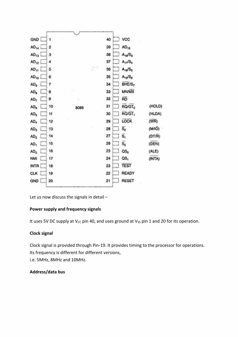
Let us now discuss the signals in detail −
Power supply and frequency signals
It uses 5V DC supply at VCC pin 40, and uses ground at VSS pin 1 and 20 for its operation.
Clock signal
Clock signal is provided through Pin-19. It provides timing to the processor for operations.
Its frequency is different for different versions,
i.e. 5MHz, 8MHz and 10MHz.
Address/data bus
115
AD0-AD15. These are 16 address/data bus. AD0-AD7 carries low order byte data and
AD8AD15 carries higher order byte data. During the first clock cycle, it carries 16-bit
address and after that it carries 16-bit data.
Address/status bus
A16-A19/S3-S6. These are the 4 address/status buses. During the first clock cycle, it carries
4-bit address and later it carries status signals.
S7/BHE
BHE stands for Bus High Enable. It is available at pin 34 and used to indicate the transfer of
data using data bus D8-D15. This signal is low during the first clock cycle, thereafter it is
active.
Read($\overline{RD}$)
It is available at pin 32 and is used to read signal for Read operation.
Ready
It is available at pin 32. It is an acknowledgement signal from I/O devices that data is
transferred. It is an active high signal. When it is high, it indicates that the device is ready to
transfer data. When it is low, it indicates wait state.
RESET
It is available at pin 21 and is used to restart the execution. It causes the processor to
immediately terminate its present activity. This signal is active high for the first 4 clock
cycles to RESET the microprocessor.
INTR
It is available at pin 18. It is an interrupt request signal, which is sampled during the last
clock cycle of each instruction to determine if the processor considered this as an interrupt
or not.
NMI
It stands for non-maskable interrupt and is available at pin 17. It is an edge triggered input,
which causes an interrupt request to the microprocessor.
116
$\overline{TEST}$
This signal is like wait state and is available at pin 23. When this signal is high, then the
processor has to wait for IDLE state, else the execution continues.
MN/$\overline{MX}$
It stands for Minimum/Maximum and is available at pin 33. It indicates what mode the
processor is to operate in; when it is high, it works in the minimum mode and vice-versa.
INTA
It is an interrupt acknowledgement signal and id available at pin 24. When the
microprocessor receives this signal, it acknowledges the interrupt.
ALE
It stands for address enable latch and is available at pin 25. A positive pulse is generated
each time the processor begins any operation. This signal indicates the availability of a valid
address on the address/data lines.
DEN
It stands for Data Enable and is available at pin 26. It is used to enable Transreceiver 8286.
The transreceiver is a device used to separate data from the address/data bus.
DT/R
It stands for Data Transmit/Receive signal and is available at pin 27. It decides the direction
of data flow through the transreceiver. When it is high, data is transmitted out and vice-a-
versa.
M/IO
This signal is used to distinguish between memory and I/O operations. When it is high, it
indicates I/O operation and when it is low indicates the memory operation. It is available at
pin 28.
117
WR
It stands for write signal and is available at pin 29. It is used to write the data into the
memory or the output device depending on the status of M/IO signal.
HLDA
It stands for Hold Acknowledgement signal and is available at pin 30. This signal
acknowledges the HOLD signal.
HOLD
This signal indicates to the processor that external devices are requesting to access the
address/data buses. It is available at pin 31.
QS1 and QS0
These are queue status signals and are available at pin 24 and 25. These signals provide the
status of instruction queue. Their conditions are shown in the following table −
QS0 QS1 Status
0 0 No operation
0 1 First byte of opcode from the queue
1 0 Empty the queue
1 1 Subsequent byte from the queue
S0, S1, S2
These are the status signals that provide the status of operation, which is used by the Bus
Controller 8288 to generate memory & I/O control signals. These are available at pin 26,
27, and 28. Following is the table showing their status −
118
S2 S1 S0 Status
0 0 0 Interrupt acknowledgement
0 0 1 I/O Read
0 1 0 I/O Write
0 1 1 Halt
1 0 0 Opcode fetch
1 0 1 Memory read
1 1 0 Memory write
1 1 1 Passive
LOCK
When this signal is active, it indicates to the other processors not to ask the CPU to leave
the system bus. It is activated using the LOCK prefix on any instruction and is available at
pin 29.
RQ/GT1 and RQ/GT0
These are the Request/Grant signals used by the other processors requesting the CPU to
release the system bus. When the signal is received by CPU, then it sends acknowledgment.
RQ/GT0 has a higher priority than RQ/GT1.
he 8086 microprocessor supports 8 types of instructions −
• Data Transfer Instructions
• Arithmetic Instructions
• Bit Manipulation Instructions
119
• String Instructions
• Program Execution Transfer Instructions (Branch & Loop Instructions)
• Processor Control Instructions
• Iteration Control Instructions
• Interrupt Instructions
Let us now discuss these instruction sets in detail.
Data Transfer Instructions These instructions are used to transfer the data from the source operand to the destination
operand. Following are the list of instructions under this group −
Instruction to transfer a word
• MOV − Used to copy the byte or word from the provided source to the provided destination.
• PUSH − Used to put a word at the top of the stack.
• POP − Used to get a word from the top of the stack to the provided location.
• PUSHA − Used to put all the registers into the stack.
• POPA − Used to get words from the stack to all registers.
• XCHG − Used to exchange the data from two locations.
• XLAT − Used to translate a byte in AL using a table in the memory.
Instructions for input and output port transfer
• IN − Used to read a byte or word from the provided port to the accumulator.
• OUT − Used to send out a byte or word from the accumulator to the provided port.
Instructions to transfer the address
• LEA − Used to load the address of operand into the provided register.
• LDS − Used to load DS register and other provided register from the memory
120
• LES − Used to load ES register and other provided register from the memory.
Instructions to transfer flag registers
• LAHF − Used to load AH with the low byte of the flag register.
• SAHF − Used to store AH register to low byte of the flag register.
• PUSHF − Used to copy the flag register at the top of the stack.
• POPF − Used to copy a word at the top of the stack to the flag register.
Arithmetic Instructions These instructions are used to perform arithmetic operations like
addition, subtraction, multiplication, division, etc.
Following is the list of instructions under this group −
Instructions to perform addition
• ADD − Used to add the provided byte to byte/word to word.
• ADC − Used to add with carry.
• INC − Used to increment the provided byte/word by 1.
• AAA − Used to adjust ASCII after addition.
• DAA − Used to adjust the decimal after the addition/subtraction operation.
Instructions to perform subtraction
• SUB − Used to subtract the byte from byte/word from word.
• SBB − Used to perform subtraction with borrow.
• DEC − Used to decrement the provided byte/word by 1.
• NPG − Used to negate each bit of the provided byte/word and add 1/2’s complement.
• CMP − Used to compare 2 provided byte/word.
• AAS − Used to adjust ASCII codes after subtraction.
121
• DAS − Used to adjust decimal after subtraction.
Instruction to perform multiplication
• MUL − Used to multiply unsigned byte by byte/word by word.
• IMUL − Used to multiply signed byte by byte/word by word.
• AAM − Used to adjust ASCII codes after multiplication.
Instructions to perform division
• DIV − Used to divide the unsigned word by byte or unsigned double word by word.
• IDIV − Used to divide the signed word by byte or signed double word by word.
• AAD − Used to adjust ASCII codes after division.
• CBW − Used to fill the upper byte of the word with the copies of sign bit of the lower byte.
• CWD − Used to fill the upper word of the double word with the sign bit of the lower word.
Bit Manipulation Instructions These instructions are used to perform operations where data bits are involved, i.e.
operations like logical, shift, etc.
Following is the list of instructions under this group −
Instructions to perform logical operation
• NOT − Used to invert each bit of a byte or word.
• AND − Used for adding each bit in a byte/word with the corresponding bit in another byte/word.
• OR − Used to multiply each bit in a byte/word with the corresponding bit in another byte/word.
• XOR − Used to perform Exclusive-OR operation over each bit in a byte/word with the
corresponding bit in another byte/word.
122
• TEST − Used to add operands to update flags, without affecting operands.
Instructions to perform shift operations
• SHL/SAL − Used to shift bits of a byte/word towards left and put zero(S) in LSBs.
• SHR − Used to shift bits of a byte/word towards the right and put zero(S) in MSBs.
• SAR − Used to shift bits of a byte/word towards the right and copy the old MSB into the new
MSB.
Instructions to perform rotate operations
• ROL − Used to rotate bits of byte/word towards the left, i.e. MSB to LSB and to Carry Flag [CF].
• ROR − Used to rotate bits of byte/word towards the right, i.e. LSB to MSB and to Carry Flag [CF].
• RCR − Used to rotate bits of byte/word towards the right, i.e. LSB to CF and CF to MSB.
• RCL − Used to rotate bits of byte/word towards the left, i.e. MSB to CF and CF to LSB.
String Instructions String is a group of bytes/words and their memory is always allocated in a sequential order.
Following is the list of instructions under this group −
• REP − Used to repeat the given instruction till CX ≠ 0.
• REPE/REPZ − Used to repeat the given instruction until CX = 0 or zero flag ZF = 1.
• REPNE/REPNZ − Used to repeat the given instruction until CX = 0 or zero flag ZF = 1.
• MOVS/MOVSB/MOVSW − Used to move the byte/word from one string to another.
123
• COMS/COMPSB/COMPSW − Used to compare two string bytes/words.
• INS/INSB/INSW − Used as an input string/byte/word from the I/O port to the provided memory
location.
• OUTS/OUTSB/OUTSW − Used as an output string/byte/word from the provided memory
location to the I/O port.
• SCAS/SCASB/SCASW − Used to scan a string and compare its byte with a byte in AL or string
word with a word in AX.
• LODS/LODSB/LODSW − Used to store the string byte into AL or string word into AX.
Program Execution Transfer Instructions (Branch and Loop Instructions) These instructions are used to transfer/branch the instructions during an execution. It
includes the following instructions −
Instructions to transfer the instruction during an execution without any condition −
• CALL − Used to call a procedure and save their return address to the stack.
• RET − Used to return from the procedure to the main program.
• JMP − Used to jump to the provided address to proceed to the next instruction.
Instructions to transfer the instruction during an execution with some conditions −
• JA/JNBE − Used to jump if above/not below/equal instruction satisfies.
• JAE/JNB − Used to jump if above/not below instruction satisfies.
• JBE/JNA − Used to jump if below/equal/ not above instruction satisfies.
• JC − Used to jump if carry flag CF = 1
• JE/JZ − Used to jump if equal/zero flag ZF = 1
124
• JG/JNLE − Used to jump if greater/not less than/equal instruction satisfies.
• JGE/JNL − Used to jump if greater than/equal/not less than instruction satisfies.
• JL/JNGE − Used to jump if less than/not greater than/equal instruction satisfies.
• JLE/JNG − Used to jump if less than/equal/if not greater than instruction satisfies.
• JNC − Used to jump if no carry flag (CF = 0)
• JNE/JNZ − Used to jump if not equal/zero flag ZF = 0
• JNO − Used to jump if no overflow flag OF = 0
• JNP/JPO − Used to jump if not parity/parity odd PF = 0
• JNS − Used to jump if not sign SF = 0
• JO − Used to jump if overflow flag OF = 1
• JP/JPE − Used to jump if parity/parity even PF = 1
• JS − Used to jump if sign flag SF = 1
Processor Control Instructions These instructions are used to control the processor action by
setting/resetting the flag values.
Following are the instructions under this group −
• STC − Used to set carry flag CF to 1
• CLC − Used to clear/reset carry flag CF to 0
• CMC − Used to put complement at the state of carry flag CF.
• STD − Used to set the direction flag DF to 1
• CLD − Used to clear/reset the direction flag DF to 0
• STI − Used to set the interrupt enable flag to 1, i.e., enable INTR input.
125
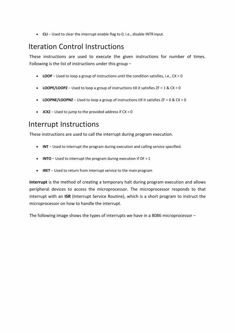
• CLI − Used to clear the interrupt enable flag to 0, i.e., disable INTR input.
Iteration Control Instructions These instructions are used to execute the given instructions for number of times.
Following is the list of instructions under this group −
• LOOP − Used to loop a group of instructions until the condition satisfies, i.e., CX = 0
• LOOPE/LOOPZ − Used to loop a group of instructions till it satisfies ZF = 1 & CX = 0
• LOOPNE/LOOPNZ − Used to loop a group of instructions till it satisfies ZF = 0 & CX = 0
• JCXZ − Used to jump to the provided address if CX = 0
Interrupt Instructions These instructions are used to call the interrupt during program execution.
• INT − Used to interrupt the program during execution and calling service specified.
• INTO − Used to interrupt the program during execution if OF = 1
• IRET − Used to return from interrupt service to the main program
Interrupt is the method of creating a temporary halt during program execution and allows
peripheral devices to access the microprocessor. The microprocessor responds to that
interrupt with an ISR (Interrupt Service Routine), which is a short program to instruct the
microprocessor on how to handle the interrupt.
The following image shows the types of interrupts we have in a 8086 microprocessor −
126
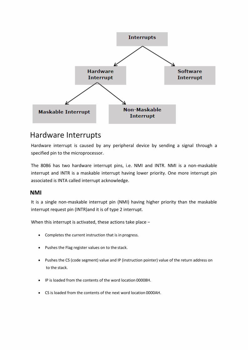
Hardware Interrupts Hardware interrupt is caused by any peripheral device by sending a signal through a
specified pin to the microprocessor.
The 8086 has two hardware interrupt pins, i.e. NMI and INTR. NMI is a non-maskable
interrupt and INTR is a maskable interrupt having lower priority. One more interrupt pin
associated is INTA called interrupt acknowledge.
NMI
It is a single non-maskable interrupt pin (NMI) having higher priority than the maskable
interrupt request pin (INTR)and it is of type 2 interrupt.
When this interrupt is activated, these actions take place −
• Completes the current instruction that is in progress.
• Pushes the Flag register values on to the stack.
• Pushes the CS (code segment) value and IP (instruction pointer) value of the return address on
to the stack.
• IP is loaded from the contents of the word location 00008H.
• CS is loaded from the contents of the next word location 0000AH.
127
• Interrupt flag and trap flag are reset to 0.
INTR
The INTR is a maskable interrupt because the microprocessor will be interrupted only if
interrupts are enabled using set interrupt flag instruction. It should not be enabled using
clear interrupt Flag instruction.
The INTR interrupt is activated by an I/O port. If the interrupt is enabled and NMI is
disabled, then the microprocessor first completes the current execution and sends ‘0’ on
INTA pin twice. The first ‘0’ means INTA informs the external device to get ready and during
the second ‘0’ the microprocessor receives the 8 bit, say X, from the programmable
interrupt controller.
These actions are taken by the microprocessor −
• First completes the current instruction.
• Activates INTA output and receives the interrupt type, say X.
• Flag register value, CS value of the return address and IP value of the return address are pushed
on to the stack.
• IP value is loaded from the contents of word location X × 4
• CS is loaded from the contents of the next word location.
• Interrupt flag and trap flag is reset to 0
Software Interrupts Some instructions are inserted at the desired position into the program to create
interrupts. These interrupt instructions can be used to test the working of various interrupt
handlers. It includes −
INT- Interrupt instruction with type number
It is 2-byte instruction. First byte provides the op-code and the second byte provides the
interrupt type number. There are 256 interrupt types under this group.
Its execution includes the following steps −
128
• Flag register value is pushed on to the stack.
• CS value of the return address and IP value of the return address are pushed on to the stack.
• IP is loaded from the contents of the word location ‘type number’ × 4
• CS is loaded from the contents of the next word location.
• Interrupt Flag and Trap Flag are reset to 0
The starting address for type0 interrupt is 000000H, for type1 interrupt is 00004H similarly
for type2 is 00008H and ……so on. The first five pointers are dedicated interrupt pointers.
i.e. −
• TYPE 0 interrupt represents division by zero situation.
• TYPE 1 interrupt represents single-step execution during the debugging of a program.
• TYPE 2 interrupt represents non-maskable NMI interrupt.
• TYPE 3 interrupt represents break-point interrupt.
• TYPE 4 interrupt represents overflow interrupt.
The interrupts from Type 5 to Type 31 are reserved for other advanced microprocessors,
and interrupts from 32 to Type 255 are available for hardware and software interrupts.
INT 3-Break Point Interrupt Instruction
It is a 1-byte instruction having op-code is CCH. These instructions are inserted into the
program so that when the processor reaches there, then it stops the normal execution of
program and follows the break-point procedure.
Its execution includes the following steps −
• Flag register value is pushed on to the stack.
• CS value of the return address and IP value of the return address are pushed on to the stack.
129
MOV CX, 4929 H, ADD AX, 2387 H, MOV AL, FFH
• IP is loaded from the contents of the word location 3×4 = 0000CH
• CS is loaded from the contents of the next word location.
• Interrupt Flag and Trap Flag are reset to 0
INTO - Interrupt on overflow instruction
It is a 1-byte instruction and their mnemonic INTO. The op-code for this instruction is CEH.
As the name suggests it is a conditional interrupt instruction, i.e. it is active only when the
overflow flag is set to 1 and branches to the interrupt handler whose interrupt type
number is 4. If the overflow flag is reset then, the execution continues to the next
instruction.
Its execution includes the following steps −
• Flag register values are pushed on to the stack.
• CS value of the return address and IP value of the return address are pushed on to the stack.
• IP is loaded from the contents of word location 4×4 = 00010H
• CS is loaded from the contents of the next word location.
• Interrupt flag and Trap flag are reset to 0
The different ways in which a source operand is denoted in an instruction is known as
addressing modes. There are 8 different addressing modes in 8086 programming −
Immediate addressing mode The addressing mode in which the data operand is a part of the instruction itself is known
as immediate addressing mode.
Example
Register addressing mode It means that the register is the source of an operand for an instruction.
130
MOV AX, [1592H], MOV AL, [0300H]
MOV AX, [BX] ; Suppose the register BX contains 4895H, then the contents
; 4895H are moved to AX
ADD CX, {BX}
MOV DX, [BX+04], ADD CL, [BX+08]
MOV BX, [SI+16], ADD AL, [DI+16]
Direct addressing mode The addressing mode in which the effective address of the memory location is written
directly in the instruction.
Example
Register indirect addressing mode This addressing mode allows data to be addressed at any memory location through an
offset address held in any of the following registers: BP, BX, DI & SI.
Example
Based addressing mode In this addressing mode, the offset address of the operand is given by the sum of contents
of the BX/BP registers and 8-bit/16-bit displacement.
Example
Indexed addressing mode In this addressing mode, the operands offset address is found by adding the contents of SI
or DI register and 8-bit/16-bit displacements.
Example
Based-index addressing mode In this addressing mode, the offset address of the operand is computed by summing the
base register to the contents of an Index register.
MOV CX, AX ; copies the contents of the 16-bit AX register into ; the 16-bit CX register),
ADD BX, AX
131
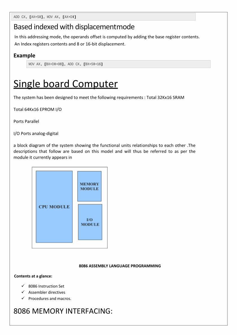
MOV AX, [BX+DI+08], ADD CX, [BX+SI+16]
Based indexed with displacement mode In this addressing mode, the operands offset is computed by adding the base register contents.
An Index registers contents and 8 or 16-bit displacement.
Example
Single board Computer The system has been designed to meet the following requirements : Total 32Kx16 SRAM
Total 64Kx16 EPROM I/O
Ports Parallel
I/O Ports analog-digital
a block diagram of the system showing the functional units relationships to each other .The descriptions that follow are based on this model and will thus be referred to as per the
module it currently appears in
8086 ASSEMBLY LANGUAGE PROGRAMMING
Contents at a glance:
✓ 8086 Instruction Set
✓ Assembler directives
✓ Procedures and macros.
8086 MEMORY INTERFACING:
ADD CX, [AX+SI], MOV AX, [AX+DI]
132
✓ 8086 addressing and address decoding ✓ Interfacing RAM, ROM, EPROM to 8086
INSTRUCTION SET OF 8086
The 8086 instructions are categorized into the following main types
(i) Data copy /transfer instructions: These type of instructions are used to transfer data from source operand
to destination operand. All the store, load, move, exchange input and output instructions belong to this
category.
(ii) Arithmetic and Logical instructions: All the instructions performing arithmetic , logical, increment,
decrement, compare and ASCII instructions belong to this category.
(iii) Branch Instructions: These instructions transfer control of execution to the specified address. All the call,
jump, interrupt and return instruction belong to this class.
(iv) Loop instructions: These instructions can be used to implement unconditional and conditional loops. The
LOOP, LOOPNZ , LOOPZ instructions belong to this category.
(v) Machine control instructions: These instructions control the machine status. NOP, HLT, WAIT and LOCK
instructions belong to this class.
(vi) Flag manipulation instructions: All the instructions which directly effect the flag register come under this
group of instructions. Instructions like CLD, STD, CLI, STI etc.., belong to this category of instructions.
(vii) Shift and Rotate instructions: These instructions involve the bit wise shifting or rotation in either direction
with or without a count in CX.
(viii) String manipulation instructions: These instructions involve various string manipulation operations like
Load, move, scan, compare, store etc..,
1. Data Copy/ Transfer Instructions:
The following instructions come under data copy / transfer instructions:
MOV PUSH POP IN OUT PUSHF POPF LEA LDS/LES XLAT
XCHG LAHF SAHF
Data Copy/ Transfer Instructions: MOV: MOVE: This data transfer instruction transfers data from one register / memory location to another register / memory location. The source may be any one of the segment register or other general purpose or special purpose registers or a memory location and another register or memory location may act as destination. Syntax: 1) MOV mem/reg1, mem/reg2
[mem/reg1] [mem/reg2] Ex: MOV BX, 0210H
MOV AL, BL MOV [SI], [BX] is not valid
Memory uses DS as segment register. No memory to memory operation is allowed. It won’t affect flag bits in the flag register.
2) MOV mem, data [mem] data
133
Ex: MOV [BX], 02H MOV [DI], 1231H
3) MOV reg, data [reg] data
Ex: MOV AL, 11H MOV CX, 1210H
4) MOV A, mem
[A] [mem] Ex: MOV AL, [SI]
MOV AX, [DI]
5) MOV mem, A [mem] A A
: AL/AX Ex: MOV [SI], AL
MOV [SI], AX
6) MOV segreg,mem/reg [segreg] [mem/reg]
Ex: MOV SS, [SI]
7) MOV mem/reg, segreg [mem/reg] [segreg]
Ex: MOV DX, SS
In the case of immediate addressing mode, a segment register cannot be destination register. In other words, direct loading of the segment registers with immediate data is not permitted. To load the segment registers with immediate data, one will have to load any general-purpose register with the data and then it will have to be moved to that particular segment register.
Ex: Load DS with 5000H 1) MOV DS, 5000H; Not permitted (invalid)
Thus to transfer an immediate data into the segment register, the convert procedure is given below:
2) MOV AX, 5000H MOV DS, AX
Both the source and destination operands cannot be memory locations (Except for string instructions)
Other MOV instructions examples are given below with the corresponding addressing modes.
3) MOV AX, 5000H; Immediate 4) MOV AX, BX; Register 5) MOV AX, [SI]; Indirect 6) MOV AX, [2000H]; Direct 7) MOV AX, 50H[BX]; Based relative, 50H displacement
PUSH: Push to Stack: This instruction pushes the contents of the specified register/memory location on to the stack. The stack pointer is decremented by 2, after each execution of the instruction. The actual current stack-top is always occupied by the previously pushed data. Hence, the push operation decrements SP by two and this store the two-byte contents of the operand onto the stack. The higher byte is pushed first and then the lower byte. Thus out of the two decremental stack addresses the higher byte occupies the higher address and the lower byte occupies the lower address.
Syntax: PUSH reg
134
[SP] [SP]-2 [[S]] [reg]
Ex: 1) PUSH AX 2) PUSH DS
3) PUSH [5000H]; content of location 5000H & 5001H in DS are pushed onto the stack.
POP: Pop from stack: This instruction when executed, loads the specified register / memory location with the contents of the memory location of which address is formed using the current stack segment and stack pointer as usual. The stack pointer is incremented by 2. The POP instruction serves exactly opposite to the PUSH instruction. Syntax:
i) POP mem [SP] [SP] +2 [mem] [[SP]]
ii) POP reg
[SP] [SP] + 2
[reg] [[SP]]
135

Ex: 1. POP AX 2. POP DS 3. POP [5000H]
XCHG: Exchange: This instruction exchanges the contents of the specified source and destination operands, which may be registers or one of them may be a memory location. However, exchange of data contents of two memory locations is not permitted.
Syntax:
i) XCHG AX, reg 16 [AX] [reg 16]
Ex: XCHG AX, DX
ii) XCHG mem, reg [mem] [reg]
Ex: XCHG [BX], DX
Register and memory can be both 8-bit and 16-bit and memory uses DS as segment register.
iii) XCHG reg, reg [reg] [ reg]
Ex: XCHG AL, CL XCHG DX, BX
Other examples:
1. XCHG [5000H], AX; This instruction exchanges data between AX and a memory location [5000H] in the data segment.
2. XCHG BX; This instruction exchanges data between AX and BX.
I/O Operations:
IN: Input the port: This instruction is used for reading an input port. The address of the input port may be specified in the instruction directly or indirectly AL and AX are the allowed destinations for 8 and 16-bit input operations. DX is the only register (implicit), which is allowed to carry the port address.
Ex: 1. IN AL, DX
[AL] [PORT DX] Input AL with the 8-bit contents of the port addressed by DX
2. IN AX, DX [AX] [PORT DX]
3. IN AL, PORT [AL] [PORT]
4. IN AX, PORT [AX] [PORT]
5. IN AL, 0300H; This instruction reads data from an 8-bit port whose
address is 0300H and stores it in AL.
6. IN AX ; This instruction reads data from a 16-bit port whose address is in DX (implicit) and stores it in AX.
OUT: Output to the Port: This instruction is used for writing to an output port.The address of the output port may be specified in the instruction directly or implicitly in DX. Contents of AX or AL are transferred to a directly or indirectly addressed port after execution of this instruction. The data to an odd addressed port is transferred on D8 –D15 while that to an even addressed port is transferred on D0-D7.The registers AL and AX are the allowed source operands for 8- bit and 16-bit
136

operations respectively.
Ex: 1. OUTDX,AL [PORT DX] [AL]
2. OUT DX,AX [PORT DX] [AX]
3. OUT PORT,AL [PORT] [AL]
4. OUT PORT,AX [PORT] [AX]
Output the 8-bit or 16-bit contents of AL or AX into an I/O port addressed by the contents of DX or local port.
5. OUT 0300H,AL; This sends data available in AL to a port whose address is 0300H 6. OUT AX; This sends data available in AX to a port whose address is specified implicitly in DX.
2. Arithmetic Instructions:
ADD ADC SUB SBB MUL IMUL DIV IDIV CMP NEGATE
INC DEC DAA DAS AAA AAS AAM AAD CBW CWD
These instructions usually perform the arithmetic operations, like addition, subtraction, multiplication and division along with the respective ASCII and decimal adjust instructions. The increment and decrement operations also belong to this type of instructions. The arithmetic instructions affect all the conditional code flags. The operands are either the registers or memory locations immediate data depending upon the addressing mode.
ADD: Addition: This instruction adds an immediate data or contents of a memory location specified in the instruction or a register (source) to the contents of another register (destination) or memory location. The result is in the destination operand. However, both the source and destination operands cannot be memory operands. That means memory to memory addition is not possible. Also the contents of the segment registers cannot be added using this instruction. All the condition code flags are affected depending upon the result.
Syntax: i. ADD mem/reg1, mem/reg2
[mem/reg1] [mem/reg2] + [mem/reg2]
Ex : ADD BL, [ST]
ADD AX, BX
ii. ADD mem, data [mem] [mem]+data
Ex: ADD Start, 02H ADD [SI], 0712H
iii. ADD reg, data
[reg] [reg]+data Ex: ADD CL, 05H
ADD DX, 0132H
iv. ADD A, data [A] [A]+data
Ex: ADD AL, 02H ADD AX, 1211H
Examples with addressing modes:
1. ADD AX, 0100H Immediate 2. ADD AX, BX Register 3. ADD AX, [SI] Register Indirect 4. ADD AX, [5000H] Direct 5. ADD [5000H], 0100H Immediate 6. ADD 0100H Destination AX (implicit)
137

ADC: Add with carry: This instruction performs the same operation as ADD instruction, but adds the carry flag bit (which may be set as a result of the previous calculations) to the result. All the condition code flags are affected by this instruction.
Syntax: i. ADC mem/reg1, mem/reg2 [mem/reg1] [mem/reg1]+[mem/reg2]+CY
Ex: ADC BL, [SI]
ADC AX, BX
ii. ADC mem,data [mem] [mem]+data+CY
Ex: ADC start, 02H ADC [SI],0712H
iii. ADC reg, data
[reg] [reg]+data+CY Ex: ADC AL, 02H
ADC AX, 1211H
Examples with addressing modes:
1. ADC 0100H Immediate(AX implicit) 2. ADC AX,BX Register 3. ADC AX,[SI] Register indirect 4. ADC AX,[5000H] Direct 5. ADC [5000H],0100H Immediate
SUB: Subtract: The subtract instruction subtracts the source operand from the destination operand and the result is left in the destination operand. Source operand may be a register or a memory location, but source and destination operands both must not be memory operands. Destination operand cannot be an immediate data. All the condition code flags are affected by this instruction.
Syntax: i. Sub mem/reg1, mem/reg2
[mem/reg1] [mem/reg2]-[mem/reg2] Ex: SUB BL,[SI] SUB AX, BX
ii. SUB mem/data [mem] [mem]-data
Ex: SUB start, 02H SUB [SI],0712H
iii. SUB A,data [A] [A]-data
Ex: SUB AL, 02H SUB AX, 1211H
Examples with addressing modes:
1. SUB 0100H Immediate [destination AX] 2. SUB AX, BX Register 3. SUB AX,[5000H] Direct 4. SUB [5000H], 0100 Immediate
SBB: Subtract with Borrow: The subtract with borrow instruction subtracts the source operand and the borrow flag (CF)which may reflect the result of the previous calculations, from the destination operand .Subtraction with borrow ,here means subtracting 1 from the subtraction obtained by SUB ,if carry (borrow) flag is set.
The result is stored in the destination operand. All the conditional code flags are affected by this instruction.
Syntax: i. SBB mem/reg1,mem/reg2
138
[mem/reg1] [mem/reg1]-[mem/reg2]-CY Ex: SBB BL,[SI]
SBB AX,BX
ii. SBB mem,data [mem] [mem]-data-CY Ex: SBB Start,02H
SBB [SI],0712H
iii. SBB reg,data [reg] [reg]-data-CY
Ex: SBB CL,05H
SBB DX,0132H
iv. SBB A,data
[A] [A]-data-CY
Ex: SBB AL,02H SBB AX,1211H
INC: Increment: This instruction increments the contents of the specified register or memory location by 1. All the condition flags are affected except the carry flag CF. This instruction adds a to the content of the operand. Immediate data cannot be operand of this instruction.
Syntax: i. INC reg16 [reg 16] [reg 16]+1
Ex: INC BX
ii. INC mem/reg 8 [mem] [mem]+1 [reg 8] [reg 8]+1
Ex: INC BL
INC SI
Segment register cannot be incremented. This operation does not affect the carry flag.
Examples with addressing modes: 1. INC AX Register 2. INC [BX] Register indirect 3. INC [5000H] Direct
DEC: Decrement: The decrement instruction subtracts 1 from the contents of the specified register or memory location. All the condition code flags except carry flag are affected depending upon the result. Immediate data cannot be operand of the instruction.
Syntax: i.
Ex:
DEC reg16
[reg 16] [reg 16]-1 DEC BX
ii. DEC mem/reg8
[mem] [mem-1
[reg 8] [reg 8]-1
Ex: DEC BL
139
Segment register cannot be decremented.
Examples with addressing mode:
1. DEC AX Register 2. DEC [5000H] Direct
MUL: Unsigned multiplication Byte or Word: This instruction multiplies unsigned byte or word by the content of AL. The unsigned byte or word may be in any one of the general-purpose register or memory locations. The most significant word of result is stored in DX, while the least significant word of the result is stored in AX. All the flags are modified depending upon the result. Immediate operand is not allowed in this instruction. If the most significant byte or word of the result is ‘0’ IF and OF both will be set.
Syntax: MUL mem/reg
For 8X8 [AX] [AL]*[mem8/re8] Ex: MUL BL
[AX] [AL]*[BL] For 16X16 [DX][AX] [AX]*[mem16/reg16]
Ex: MUL BX [DX][AX] [AX]*[BX]
higher lower 16-bit 16-bit
Ex: 1. MUL BH ; [AX] [AL]*[BH]
2. MUL CX ; [DX][AX] [AX*[CX] 3. MUL WORD PTR[SI];[DX][AX] [AX]*[SI]
IMUL: Signed Multiplication: This instruction multiplies a signed byte in source operand by a signed byte in AL or signed word in source operand by signed word in AX. The source can be a general purpose register, memory operand, index register or base register, but it cannot be an immediate data. In case of 32-bit results, the higher order word (MSW) is stored in DX and the lower order word is stored in AX. The AF, PF, SF and ZF flags are undefined after IMUL. If AH and DH contain parts of 16 and 32-bit result respectively, CF and OF both will of set. The AL and AX are the implicit operands in case of 8-bit and 16-bit multiplications respectively. The unused higher bits of the result are filled by sign bit and CF, AF are cleared.
Syntax: IMUL mem/reg For 8X8 [AX] [AL]*[mem8/reg8]
Ex: IMUL BL [AX] [AL]*[BL]
For 16X16
[DX][AX] [AX*[mem16/reg16] Ex: IMUL BX
[DX][AX] [AX]*[BX] Memory or register can be 8-bit or 16-bit and this instruction will affect carry flag & overflow flag.
Ex: 1. IMUL BH
2. IMUL CX 3. IMUL [SI]
DIV: Unsigned division: This instruction performs unsigned division. It divides an unsigned word or double word by a 16-bit or 8-bit operand. The dividend must be in AX for 16-bit operation and divisor may be specified using any one of the addressing modes except immediate. The result will be in AL (quotient) while AH will contain the remainder. If the result is too big to fit in AL, type 0(divide by zero) interrupt is generated. In case of a double word dividend (32-bit), the higher word should be in DX and lower word should be in AX. The divisor may be specified as already explained. The quotient and the remainder, in this case, will be in AX and DX respectively. This instruction does not affect any flag.
Syntax: DIV mem/reg
140
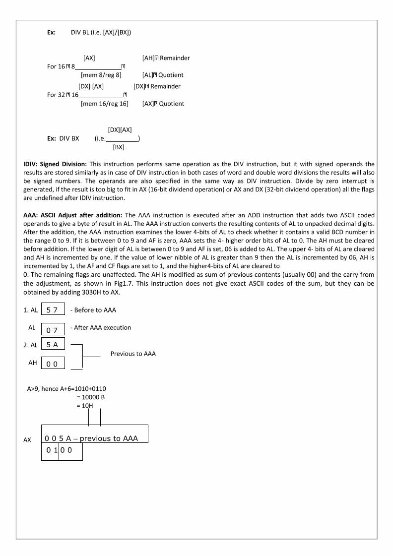
0 0 0 1
0 0 5 A – previous to AAA
0 7
5 7
Ex: DIV BL (i.e. [AX]/[BX])
[AX] [AH] Remainder
For 16 8 [mem 8/reg 8] [AL] Quotient
[DX] [AX] [DX] Remainder For 32 16
[mem 16/reg 16] [AX] Quotient
[DX][AX]
Ex: DIV BX (i.e. ) [BX]
IDIV: Signed Division: This instruction performs same operation as the DIV instruction, but it with signed operands the results are stored similarly as in case of DIV instruction in both cases of word and double word divisions the results will also be signed numbers. The operands are also specified in the same way as DIV instruction. Divide by zero interrupt is generated, if the result is too big to fit in AX (16-bit dividend operation) or AX and DX (32-bit dividend operation) all the flags are undefined after IDIV instruction.
AAA: ASCII Adjust after addition: The AAA instruction is executed after an ADD instruction that adds two ASCII coded operands to give a byte of result in AL. The AAA instruction converts the resulting contents of AL to unpacked decimal digits. After the addition, the AAA instruction examines the lower 4-bits of AL to check whether it contains a valid BCD number in the range 0 to 9. If it is between 0 to 9 and AF is zero, AAA sets the 4- higher order bits of AL to 0. The AH must be cleared before addition. If the lower digit of AL is between 0 to 9 and AF is set, 06 is added to AL. The upper 4- bits of AL are cleared and AH is incremented by one. If the value of lower nibble of AL is greater than 9 then the AL is incremented by 06, AH is incremented by 1, the AF and CF flags are set to 1, and the higher4-bits of AL are cleared to
0. The remaining flags are unaffected. The AH is modified as sum of previous contents (usually 00) and the carry from the adjustment, as shown in Fig1.7. This instruction does not give exact ASCII codes of the sum, but they can be obtained by adding 3030H to AX.
1. AL - Before to AAA
AL - After AAA execution
2. AL
AH
A>9, hence A+6=1010+0110
= 10000 B = 10H
AX
Previous to AAA
0 0
5 A
141
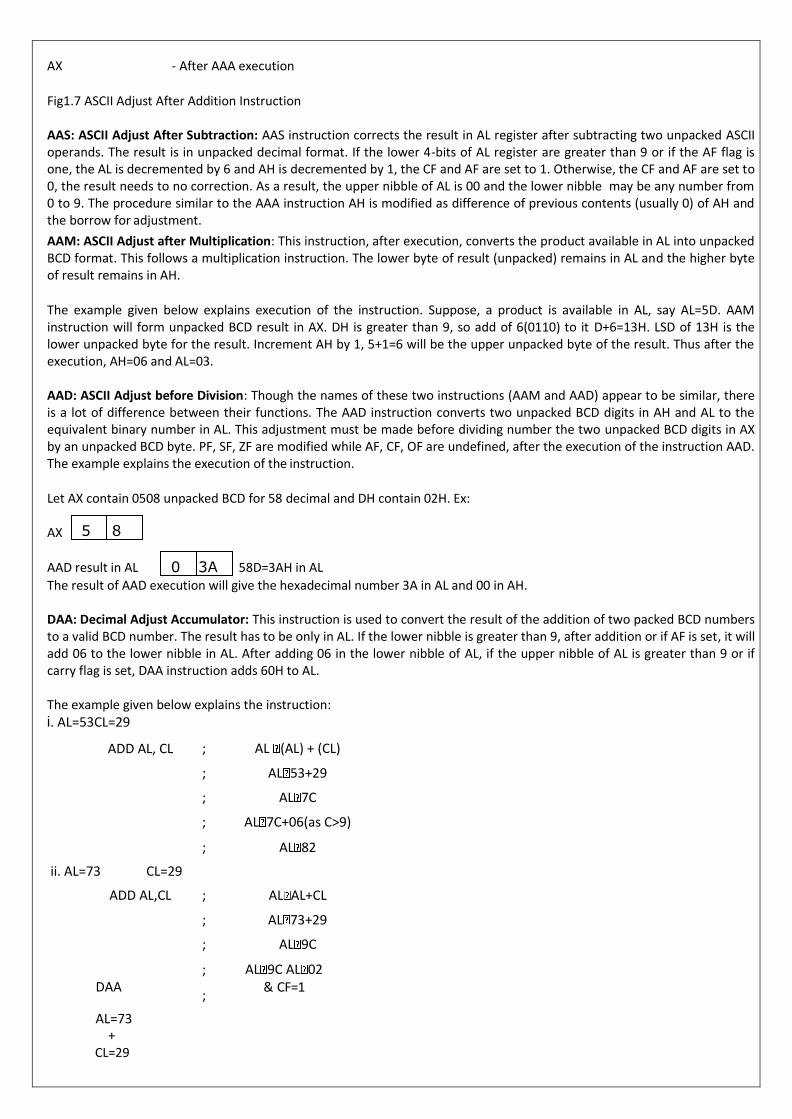
3A 0
AX - After AAA execution
Fig1.7 ASCII Adjust After Addition Instruction
AAS: ASCII Adjust After Subtraction: AAS instruction corrects the result in AL register after subtracting two unpacked ASCII operands. The result is in unpacked decimal format. If the lower 4-bits of AL register are greater than 9 or if the AF flag is one, the AL is decremented by 6 and AH is decremented by 1, the CF and AF are set to 1. Otherwise, the CF and AF are set to 0, the result needs to no correction. As a result, the upper nibble of AL is 00 and the lower nibble may be any number from 0 to 9. The procedure similar to the AAA instruction AH is modified as difference of previous contents (usually 0) of AH and the borrow for adjustment.
AAM: ASCII Adjust after Multiplication: This instruction, after execution, converts the product available in AL into unpacked BCD format. This follows a multiplication instruction. The lower byte of result (unpacked) remains in AL and the higher byte of result remains in AH.
The example given below explains execution of the instruction. Suppose, a product is available in AL, say AL=5D. AAM instruction will form unpacked BCD result in AX. DH is greater than 9, so add of 6(0110) to it D+6=13H. LSD of 13H is the lower unpacked byte for the result. Increment AH by 1, 5+1=6 will be the upper unpacked byte of the result. Thus after the execution, AH=06 and AL=03.
AAD: ASCII Adjust before Division: Though the names of these two instructions (AAM and AAD) appear to be similar, there is a lot of difference between their functions. The AAD instruction converts two unpacked BCD digits in AH and AL to the equivalent binary number in AL. This adjustment must be made before dividing number the two unpacked BCD digits in AX by an unpacked BCD byte. PF, SF, ZF are modified while AF, CF, OF are undefined, after the execution of the instruction AAD. The example explains the execution of the instruction.
Let AX contain 0508 unpacked BCD for 58 decimal and DH contain 02H. Ex:
AX
AAD result in AL 58D=3AH in AL
The result of AAD execution will give the hexadecimal number 3A in AL and 00 in AH.
DAA: Decimal Adjust Accumulator: This instruction is used to convert the result of the addition of two packed BCD numbers to a valid BCD number. The result has to be only in AL. If the lower nibble is greater than 9, after addition or if AF is set, it will add 06 to the lower nibble in AL. After adding 06 in the lower nibble of AL, if the upper nibble of AL is greater than 9 or if carry flag is set, DAA instruction adds 60H to AL.
The example given below explains the instruction:
i. AL=53CL=29
ADD AL, CL ;
;
AL (AL) + (CL)
AL 53+29
; AL 7C
; AL 7C+06(as C>9)
; AL 82
ii. AL=73 CL=29
ADD AL,CL ; AL AL+CL
; AL 73+29
; AL 9C
DAA ;
;
AL 9C AL 02 & CF=1
AL=73
+ CL=29
8 5
142
9C +6
A2
+60
CF=1 02 in AL The instruction DAA affects AF, CF, PF and ZF flags. The OF flag is undefined.
DAS: Decimal Adjust After Subtraction: This instruction converts the results of subtraction of two packed BCD numbers to a valid BCD number. The subtraction has to be in AL only. If the lower nibble of AL is greater than 9, this instruction will subtract 06 from lower nibble of AL. If the result of subtractions sets the carry flag or if upper nibble is greater than 9, it subtracts 60H from AL. This instruction modifier the AF, CF, PF and ZF flags. The OF is undefined after DAS instruction.
The examples are as follows:
Ex: i. AL=75 BH=46 SUB AL,BH ; AL 2F=(AL)-(BH)
; AF=1 DAS ; AL 29 (as F>9,F-6=9)
ii. AL=38 CH=61 SUB AL, CH ; AL D7 CF=1(borrow) DAS ; AL 77(as D>9, D-6=7)
; CF=1(borrow)
NEG: Negate: The negate instruction forms 2’s complement of the specified destination in the instruction. For obtaining 2’s complement, it subtracts the contents of destination from zero. The result is stored back in the destination operand which may be a register or a memory location. If OF is set, it indicates that the operation could not be completed successfully. This instruction affects all the condition code flags.
CBW: Convert signed Byte to Word: This instruction converts a signed byte to a signed word. In other words, it copies the sign bit of a byte to be converted to all the bits in the higher byte of the result word. The byte to be converted must be in AL. The result will be in AX. It does not affect any flag.
CWD: Convert Signed Word to double Word: This instruction copies the sign bit of AX to all the bits of DX register. This operation is to be done before signed division. It does not affect any other flag.
3. Logical Instructions:
AND OR NOT XOR TEST
These byte of instructions are used for carrying out the bit by bit shift, rotate or basic logical operations. All the conditional code flags are affected depending upon the result. Basic logical operations available with 8086 instruction set an AND, OR, NOT and XOR.
AND: Logical AND: This instruction bit by bit ANDs the source operand that may be an immediate, a register, or a memory location to the destination operand that may be a register or a memory location. The result is stored in the destination operand. At least one of the operand should be a register or a memory operand. Both the operands cannot be memory locations or immediate operand.
The examples of this instruction are as follows:
Syntax: i. AND mem/reg1, mem/reg2 [mem/reg1] [mem/reg1] [mem/reg2]
Ex: AND BL, CH
143
ii. AND mem,data [mem] [mem] data
Ex: AND start,05H
iii. AND reg,data [reg] [reg] data
Ex: AND AL, FOH
iv. AND A,data [A] [A] data A:AL/AX
Ex: AND AX,1021H
OR: Logical OR: The OR instruction carries out the OR operation in the same way as described in case of the AND operation. The limitations on source and destination operands are also the same as in case of AND operation.
Syntax: i. OR mem/reg1, mem/reg2 [mem/reg1] [mem/reg1] [mem/reg2]
Ex: OR BL, CH
ii. OR mem,data [mem [mem] data
Ex: OR start, 05H
iii. OR Start,05H [reg] [reg] data
Ex: OR AL, FOH
iv. OR A, data [A] [A] data
Ex: OR AL, 1021H A: AL/AX.
NOT: Logical Invert: The NOT instruction complements (invents) the contents of an operand register or a memory location bit by bit.
Syntax: i.
Ex:
NOT reg
[reg] [reg]
NOT AX
ii. NOT mem [mem] [mem]
Ex: NOT [SI]
XOR: Logical Exclusive OR: The XOR operation is again carried out in a similar way to the AND and OR operation. The constraints on high output, when the 2 input bits are dissimilar. Otherwise, the output is zero.
Syntax: i. XOR mem/reg1, mem/reg2
[mem/reg1] [mem/reg1] [mem/reg2]
Ex: XOR BL, CH
ii. XOR mem,data [mem] [mem] data
Ex: XOR start, 05H
144
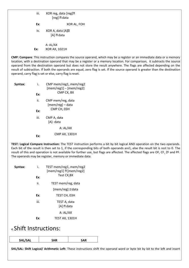
iii. XOR reg, data [reg] [reg] data
Ex: XOR AL, FOH
iv. XOR A, data [A]
[A] data
A: AL/AX
Ex: XOR AX, 1021H
CMP: Compare: This instruction compares the source operand, which may be a register or an immediate data or a memory location, with a destination operand that may be a register or a memory location. For comparison, it subtracts the source operand from the destination operand but does not store the result anywhere. The flags are affected depending on the result of subtraction. If both the operands are equal, zero flag is set. If the source operand is greater than the destination operand, carry flag is set or else, carry flag is reset.
Syntax: i.
Ex:
CMP mem/reg1, mem/reg2 [mem/reg1] – [mem/reg2]
CMP CX, BX
ii.
Ex:
CMP mem/reg, data [mem/reg] – data
CMP CH, 03H
iii.
Ex:
CMP A, data [A]- data
A: AL/AX
CMP AX, 1301H
TEST: Logical Compare Instruction: The TEST instruction performs a bit by bit logical AND operation on the two operands. Each bit of the result is then set to 1, if the corresponding bits of both operands are1, else the result bit is rest to 0. The result of this and operation is not available for further use, but flags are affected. The affected flags are OF, CF, ZF and PF. The operands may be register, memory or immediate data.
Syntax: i.
Ex:
TEST mem/reg1, mem/reg2 [mem/reg1] [mem/reg2]
Test CX,BX
ii. TEST mem/reg, data
[mem/reg] data
Ex: TEST CH, 03H
iii. TEST A, data [A] data
A: AL/AX
Ex: TEST AX, 1301H
4. Shift Instructions:
SHL/SAL SHR SAR
SHL/SAL: Shift Logical/ Arithmetic Left: These instructions shift the operand word or byte bit by bit to the left and insert
145
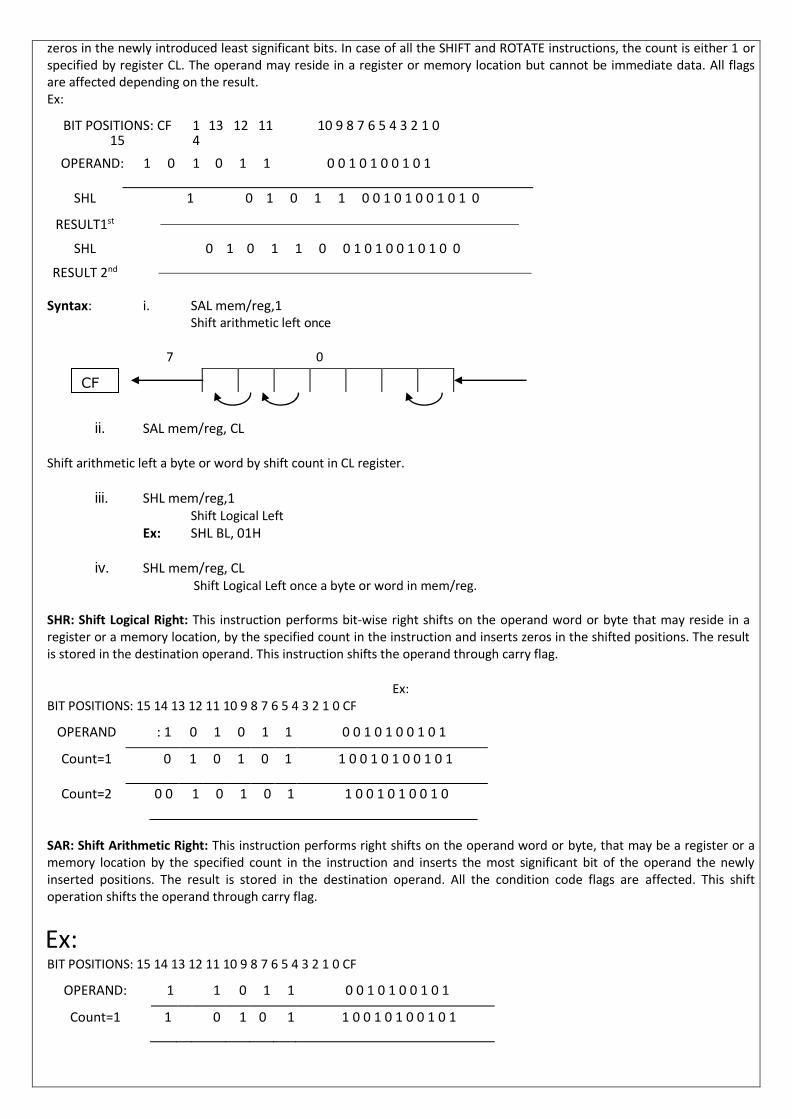
0
zeros in the newly introduced least significant bits. In case of all the SHIFT and ROTATE instructions, the count is either 1 or specified by register CL. The operand may reside in a register or memory location but cannot be immediate data. All flags are affected depending on the result. Ex:
BIT POSITIONS: CF 15
14
13 12 11 10 9 8 7 6 5 4 3 2 1 0
OPERAND: 1 0 1 0 1 1 0 0 1 0 1 0 0 1 0 1
SHL 1 0 1 0 1 1 0 0 1 0 1 0 0 1 0 1 0
RESULT1st
SHL 0 1 0 1 1 0 0 1 0 1 0 0 1 0 1 0 0
RESULT 2nd
Syntax: i. SAL mem/reg,1 Shift arithmetic left once
7 0
ii. SAL mem/reg, CL
Shift arithmetic left a byte or word by shift count in CL register.
iii. SHL mem/reg,1
Shift Logical Left
Ex: SHL BL, 01H
iv. SHL mem/reg, CL Shift Logical Left once a byte or word in mem/reg.
SHR: Shift Logical Right: This instruction performs bit-wise right shifts on the operand word or byte that may reside in a register or a memory location, by the specified count in the instruction and inserts zeros in the shifted positions. The result is stored in the destination operand. This instruction shifts the operand through carry flag.
Ex:
BIT POSITIONS: 15 14 13 12 11 10 9 8 7 6 5 4 3 2 1 0 CF
OPERAND : 1 0 1 0 1 1 0 0 1 0 1 0 0 1 0 1
Count=1 0 1 0 1 0 1 1 0 0 1 0 1 0 0 1 0 1
Count=2 0 0 1 0 1 0 1 1 0 0 1 0 1 0 0 1 0
SAR: Shift Arithmetic Right: This instruction performs right shifts on the operand word or byte, that may be a register or a memory location by the specified count in the instruction and inserts the most significant bit of the operand the newly inserted positions. The result is stored in the destination operand. All the condition code flags are affected. This shift operation shifts the operand through carry flag.
Ex: BIT POSITIONS: 15 14 13 12 11 10 9 8 7 6 5 4 3 2 1 0 CF
OPERAND: 1 0 1 0 1 1 0 0 1 0 1 0 0 1 0 1
Count=1 1 1 0 1 0 1 1 0 0 1 0 1 0 0 1 0 1
CF
146
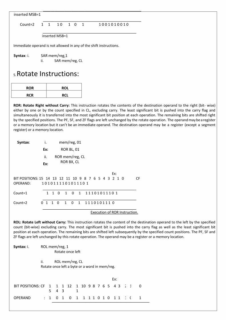
inserted MSB=1
Count=2 1 1 1 0 1 0 1 1 0 0 1 0 1 0 0 1 0
inserted MSB=1
Immediate operand is not allowed in any of the shift instructions.
Syntax: i. SAR mem/reg,1 ii. SAR mem/reg, CL
5. Rotate Instructions:
ROR ROL
RCR RCL
ROR: Rotate Right without Carry: This instruction rotates the contents of the destination operand to the right (bit- wise) either by one or by the count specified in CL, excluding carry. The least significant bit is pushed into the carry flag and simultaneously it is transferred into the most significant bit position at each operation. The remaining bits are shifted right by the specified positions. The PF, SF, and ZF flags are left unchanged by the rotate operation. The operand may be a register or a memory location but it can’t be an immediate operand. The destination operand may be a register (except a segment register) or a memory location.
Syntax: i.
Ex:
mem/reg, 01
ROR BL, 01
ii.
Ex:
ROR mem/reg, CL ROR BX, CL
Ex:
BIT POSITIONS: 15 14 13 12 11 10 9 8 7 6 5 4 3 2 1 0 CF OPERAND: 1 0 1 0 1 1 1 1 0 1 0 1 1 1 0 1
_ Count=1 1 1 0 1 0 1 1 1 1 0 1 0 1 1 1 0 1
Count=2 0 1 1 0 1 0 1 1 1 1 0 1 0 1 1 1 0
Execution of ROR Instruction.
ROL: Rotate Left without Carry: This instruction rotates the content of the destination operand to the left by the specified count (bit-wise) excluding carry. The most significant bit is pushed into the carry flag as well as the least significant bit position at each operation. The remaining bits are shifted left subsequently by the specified count positions. The PF, SF and ZF flags are left unchanged by this rotate operation. The operand may be a register or a memory location.
Syntax: i. ROL mem/reg, 1 Rotate once left
ii. ROL mem/reg, CL Rotate once left a byte or a word in mem/reg.
Ex:
BIT POSITIONS: CF 15
14
13
12 11
10 9 8 7 6 5 4 3 2 1 0
OPERAND : 1 0 1 0 1 1 1 1 0 1 0 1 1 1 0 1
147
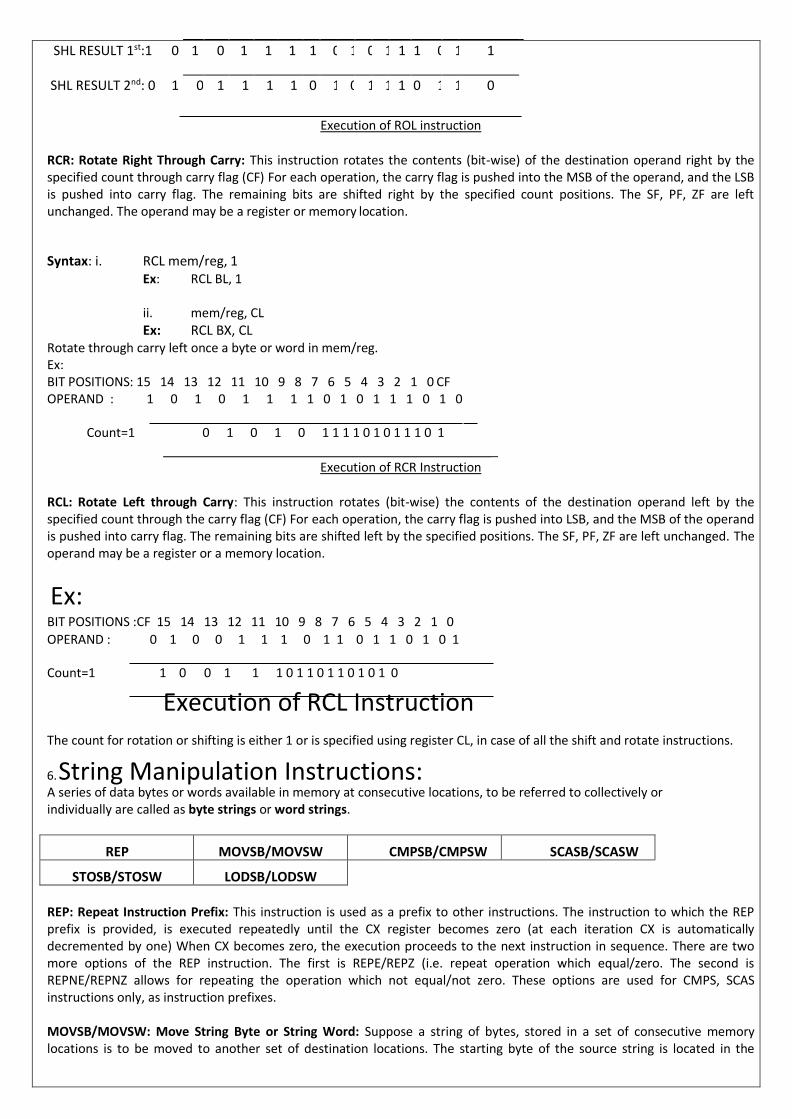
SHL RESULT 1st:1 0 1 0 1 1 1 1 0 1 0 1 1 1 0 1 1
SHL RESULT 2nd: 0 1 0 1 1 1 1 0 1 0 1 1 1 0 1 1 0
Execution of ROL instruction
RCR: Rotate Right Through Carry: This instruction rotates the contents (bit-wise) of the destination operand right by the specified count through carry flag (CF) For each operation, the carry flag is pushed into the MSB of the operand, and the LSB is pushed into carry flag. The remaining bits are shifted right by the specified count positions. The SF, PF, ZF are left unchanged. The operand may be a register or memory location.
Syntax: i. RCL mem/reg, 1 Ex: RCL BL, 1
ii. mem/reg, CL
Ex: RCL BX, CL Rotate through carry left once a byte or word in mem/reg. Ex: BIT POSITIONS: 15 14 13 12 11 10 9 8 7 6 5 4 3 2 1 0 CF OPERAND : 1 0 1 0 1 1 1 1 0 1 0 1 1 1 0 1 0
Count=1 0 1 0 1 0 1 1 1 1 0 1 0 1 1 1 0 1
_ Execution of RCR Instruction
RCL: Rotate Left through Carry: This instruction rotates (bit-wise) the contents of the destination operand left by the specified count through the carry flag (CF) For each operation, the carry flag is pushed into LSB, and the MSB of the operand is pushed into carry flag. The remaining bits are shifted left by the specified positions. The SF, PF, ZF are left unchanged. The operand may be a register or a memory location.
Ex: BIT POSITIONS :CF 15 14 13 12 11 10 9 8 7 6 5 4 3 2 1 0
OPERAND : 0 1 0 0 1 1 1 0 1 1 0 1 1 0 1 0 1
Count=1 1 0 0 1 1 1 0 1 1 0 1 1 0 1 0 1 0
Execution of RCL Instruction
The count for rotation or shifting is either 1 or is specified using register CL, in case of all the shift and rotate instructions.
6. String Manipulation Instructions:
A series of data bytes or words available in memory at consecutive locations, to be referred to collectively or individually are called as byte strings or word strings.
REP MOVSB/MOVSW CMPSB/CMPSW SCASB/SCASW
STOSB/STOSW LODSB/LODSW
REP: Repeat Instruction Prefix: This instruction is used as a prefix to other instructions. The instruction to which the REP prefix is provided, is executed repeatedly until the CX register becomes zero (at each iteration CX is automatically decremented by one) When CX becomes zero, the execution proceeds to the next instruction in sequence. There are two more options of the REP instruction. The first is REPE/REPZ (i.e. repeat operation which equal/zero. The second is REPNE/REPNZ allows for repeating the operation which not equal/not zero. These options are used for CMPS, SCAS instructions only, as instruction prefixes.
MOVSB/MOVSW: Move String Byte or String Word: Suppose a string of bytes, stored in a set of consecutive memory locations is to be moved to another set of destination locations. The starting byte of the source string is located in the
148
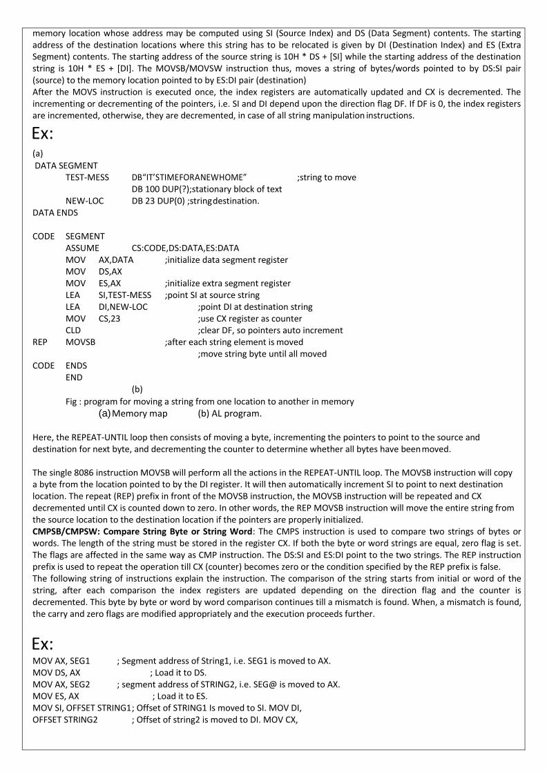
memory location whose address may be computed using SI (Source Index) and DS (Data Segment) contents. The starting address of the destination locations where this string has to be relocated is given by DI (Destination Index) and ES (Extra Segment) contents. The starting address of the source string is 10H * DS + [SI] while the starting address of the destination string is 10H * ES + [DI]. The MOVSB/MOVSW instruction thus, moves a string of bytes/words pointed to by DS:SI pair (source) to the memory location pointed to by ES:DI pair (destination) After the MOVS instruction is executed once, the index registers are automatically updated and CX is decremented. The incrementing or decrementing of the pointers, i.e. SI and DI depend upon the direction flag DF. If DF is 0, the index registers are incremented, otherwise, they are decremented, in case of all string manipulation instructions.
Ex:
(a)
DATA SEGMENT TEST-MESS DB “IT’S TIME FOR A NEW HOME” ;string to move
DB 100 DUP(?);stationary block of text NEW-LOC DB 23 DUP(0) ;string destination.
DATA ENDS
CODE SEGMENT ASSUME CS:CODE,DS:DATA,ES:DATA MOV AX,DATA ;initialize data segment register MOV DS,AX MOV ES,AX ;initialize extra segment register LEA SI,TEST-MESS ;point SI at source string LEA DI,NEW-LOC ;point DI at destination string MOV CS,23 ;use CX register as counter CLD ;clear DF, so pointers auto increment
REP MOVSB ;after each string element is moved ;move string byte until all moved
CODE ENDS END
(b)
Fig : program for moving a string from one location to another in memory (a) Memory map (b) AL program.
Here, the REPEAT-UNTIL loop then consists of moving a byte, incrementing the pointers to point to the source and destination for next byte, and decrementing the counter to determine whether all bytes have been moved.
The single 8086 instruction MOVSB will perform all the actions in the REPEAT-UNTIL loop. The MOVSB instruction will copy a byte from the location pointed to by the DI register. It will then automatically increment SI to point to next destination location. The repeat (REP) prefix in front of the MOVSB instruction, the MOVSB instruction will be repeated and CX decremented until CX is counted down to zero. In other words, the REP MOVSB instruction will move the entire string from the source location to the destination location if the pointers are properly initialized. CMPSB/CMPSW: Compare String Byte or String Word: The CMPS instruction is used to compare two strings of bytes or words. The length of the string must be stored in the register CX. If both the byte or word strings are equal, zero flag is set. The flags are affected in the same way as CMP instruction. The DS:SI and ES:DI point to the two strings. The REP instruction prefix is used to repeat the operation till CX (counter) becomes zero or the condition specified by the REP prefix is false. The following string of instructions explain the instruction. The comparison of the string starts from initial or word of the string, after each comparison the index registers are updated depending on the direction flag and the counter is decremented. This byte by byte or word by word comparison continues till a mismatch is found. When, a mismatch is found, the carry and zero flags are modified appropriately and the execution proceeds further.
Ex: MOV AX, SEG1 ; Segment address of String1, i.e. SEG1 is moved to AX. MOV DS, AX ; Load it to DS. MOV AX, SEG2 ; segment address of STRING2, i.e. SEG@ is moved to AX. MOV ES, AX ; Load it to ES. MOV SI, OFFSET STRING1 ; Offset of STRING1 Is moved to SI. MOV DI, OFFSET STRING2 ; Offset of string2 is moved to DI. MOV CX,
149
0110H ; Length of string is moved to CX.
CLD ; clear DF, i.e. set auto increment mode. REPE CMPSW ; Compare 010H words of STRING1 And STRING2, while they are equal, IF a
mismatch is found, modify the flags and proceed with further execution.
If both strings are completely equal, i.e. CX becomes zero, the ZF is set, otherwise ZF is reset.
SCAS: Scan String BYTE or String Word: This instruction scans a string of bytes or words for an operand byte or word specified in the register AL or AX. The string is pointed to by ES:DI register pair. The length of the string is stored in CX. The DF controls the mode for scanning of the string as stated in case of MOVSB instruction. Whenever a match to the specified operand, is found in the string, execution stops and the zero flag is set. If no match is found, the zero flag is reset. The REPNE prefix is used with the SCAS instruction. The pointers and counters are updated automatically, till a match is found.
Ex: MOV AX, SEG ; Segment address of the string, i.e. SEG is moved to AX. MOV ES, AX ; Load it to ES. MOV DI, OFFSET ; String offset, i.e. OFFSET is moved to DI. MOV CX,010H ; Length of the string is moved to CX. MOV AX, WORD ; The word to be scanned for, i.e. WORD is in AL. CLD ; Clear DF REPNE SCASW ; Scan the 010H bytes of the string, till a match to WORD is found.
This string of instructions finds out, if it contains WORD. IF the WORD is found in the word string, before CX becomes zero, the ZF is set, otherwise the ZF is reset. The scanning will continue till a match is found. Once a match is found the execution of the program proceeds further.
LODS: Load string Byte or String word: The LODS instruction loads the AL/AX register by the content of a string pointed to by DS:SI register pair. The SI is modified automatically depending on DF. If it is a byte transfer (LODSB), the SI is modified bye one and if it is a word transfer (LODSW), the SI is modified by two. No other flags are affected by this instruction.
STOS: Store String Byte or String Word: The STOS instruction stores the AL/AX register contents to a location in the string pointed by ES:DI register pair. The DI is modified Accordingly. No flags are affected by this instruction.
The direction flag controls the string instruction execution. The source index SI and destination index DI are modified after each iteration automatically. If DF=1, then the execution follows auto decrement mode. In this mode, SI and DI are decremented automatically after each iteration (by1 or 2 depending on byte or word operations) Hence, in auto decrementing mode, the string are referred to by their ending addresses. If DF=0, then the execution follows auto increment mode. In this mode, SI and DI are incremented automatically (by 1 or 2 depending on byte or word operation) After each iteration, hence the strings, in this case, are referred to by their starting addresses.
7. Control Transfer or Branching Instruction:
The control transfer instructions transfer the flow of execution of the program to a new address specified in the instruction directly or indirectly. When this type of instruction is executed, the CS and IP registers get loaded with new values of CS and IP corresponding to the location where the flow of execution is going to be transferred.
This type of instructions are classified in two types: i. Unconditional control Transfer (Branch) Instructions: In case of unconditional control transfer instructions; the execution control is transferred to the specified location independent of any status or condition. The CS and IP are unconditionally modified to the new CS and IP.
ii. Conditional Control Transfer (Branch) Instructions: In the conditional control transfer instructions, the control is transferred to the specified location provided the result of the previous operation satisfies a particular condition, otherwise, the execution continues in normal flow sequence. The results of the previous operations are replicated by condition code flags. In other words, using type of instruction the control will be transferred to a particular specified location, if a particular flag satisfies the condition.
150
CS(LB) CS(UB)
IP(LB) IP(UB)
DISP 16-bit
DISP 16-bit
DISP 8-bit
Unconditional Branch Instructions: CALL RET JUMP IRET
INT N INT O LOOP
CALL: Unconditional Call: This instruction is used to call a subroutine procedure from a main program. The address of the procedure may specify directly or indirectly depending on the address mode. There are again two types of procedures depending on whether it is available in the same segment (Near CALL, i.e. + 2K displacement) or in another segment (Far CALL, i.e. anywhere outside the segment). The modes for them are respectively called as intrasegment and intersegment addressing (i.e. address of the next instruction) and CS onto the stack along with the flags and loads the CS and IP registers, respectively, with the segment and offset addresses of the procedure to be called.
RET: Return from the Procedure: At each CALL instruction, the IP and CS of the next instruction is pushed onto stack, before the control is transferred to the procedure. At the end of the procedure, the RET instruction must be executed. When it is executed, the previously stored content of IP and CS along with flags are retrieved into the CS, IP and flag registers from the stack and the execution of the main program continues further. In case of a FAR procedure the current contents of SP points to IP and CS at the time of return. While in case of a NEAR procedure, it points to only IP. Depending on the byte of procedure and the SP contents, the RET instruction is of four types:
i. Return within a segment. ii. Return within a segment adding 16-bit immediate displacement to the SP contents. iii. Return intersegment. iv. Return intersegment adding 16-bit immediate displacement to the SP contents.
INT N: Interrupt Type N: In the interrupt structure of 8086/8088, 256 interrupts are defined corresponding to the types from 00H to FFH. When an INT N instruction is executed, the TYPE byte N is multiplied by 4 and the contents of IP and CS of the interrupt service routine will be taken from the hexadecimal multiplication (N * 4) as offset address and 0000 as segment address. In other words, the multiplication of type N by 4 (offset) points to a memory block in 0000 segment, which contains the IP and CS values of the interrupt service routine. For the execution of this instruction, the IP must be enabled.
Ex: The INT 20H will find out the address of the interrupt service routine follows: INT
20H Type * 4 = 20 X 4 = 80H
Pointer to IP and CS of the ISR is 0000:0080H
The arrangement of CS and IP addresses of the ISR in the interrupt rector table is as follows.
INTO: Interrupt on overflow: This is executed, when the overflow flag OF is set. The new contents of IP an CS are taken from the address 0000:0000 as explained in INT type instruction. This is equivalent to a type 4 instruction.
JMP: Unconditional Jump: This instruction unconditionally transfer the control of execution to the specified address using an 8-bit or 16-bit displacement (intrasegment relative, short or long) or CS:IP (intersegment direct for) No flags are affected by this instruction. Corresponding to the three methods of specifying jump address, the JUMP instruction has the following three formats.
JUMP Intrasegment, relative, near jump
JUMP Intrasegment, relative, For jump
JUMP Intersegment, direct, jump
IRET: Return from ISR: When interrupt service routine is to be called, before transferring control to it, the IP, CS and flag register are stored on to the stack to indicate the location from where the execution is to be continued, after the ISR is executed. So, at the end of each ISR, when IRET is executed, the valuesof IP, CS and flags are retrieved from the stack to continue the execution of the main program. The stack is modified accordingly.
151
LOOP: Loop unconditionally: This instruction executes the part of the program from the label or address specified in the instruction up to the loop instruction, CX number of times. At each iteration, CX is decremented automatically, in other words, this instruction implements DECREMENT counter and JUMP IF NOT ZERO structure.
Ex: MOV CX,0005H ; Number of times in CX MOV BX, 0FF7H ; Data to BX
Label MOV AX, CODE1 OR BX,AX AND DX,AX LOOP Label
152
The execution proceeds in sequence, after the loop is executed, CX number of times. IF CX is already 00H, the execution continues sequentially. No flags are affected by this instruction.
Conditional Branch Instructions:
When these instructions are executed, they transfer execution control to the address specified relatively in the instruction, provided the condition in the opcode is satisfied, otherwise, the execution continues sequentially. The conditions, here means the status of the condition code flags. These type of instructions don’t affect any flags. The address has to be specified in the instruction relatively in terms of displacement, which must lie within – 80H to 7FH (or –128 to 127) bytes from the address of the branch instruction. In other words, only short jumps can be implemented using conditional branch instructions. A label may represent the displacement, if it has within the above- specified range. The different 8086/8088 conditional branch instructions and their operations are listed in Table1
SL.No Mnemonic Displacement Operation
1 JZ/JE Label Transfer execution control to address ‘Label’, if ZF=1
2 JNZ/JNE Label Transfer execution control to address ‘Label’, if ZF=0
3 JS Label Transfer execution control to address ‘Label’, if SF=1
4 JNS Label Transfer execution control to address ‘Label’, if SF=0
5 JO Label Transfer execution control to address ‘Label’, if OF=1
6 JNO Label Transfer execution control to address ‘Label’, if OF=0
7 JP/JPE Label Transfer execution control to address
‘Label’, if PF=1
8 JNP Label Transfer execution control to address ‘Label’, if PF=0
9 JB/JNAE/JC Label Transfer execution control to address ‘Label’, if CF=1
10 JNB/JNE/JNC Label Transfer execution control to address ‘Label’, if CF=0
11 JBE/JNA Label Transfer execution control to address ‘Label’, if CF=1 or ZF=1
12 JNBE/JA Label Transfer execution control to address ‘Label’, if CF=0 or ZF=0
13 JL/JNGE Label Transfer execution control to address ‘Label’, if neither SF=1 nor OF=1
14 JNL/JGE Label Transfer execution control to address ‘Label’, if neither SF=0 nor OF=0
15 JNE/JNC Label Transfer execution control to address
‘Label’, if ZF=1or neither SF nor OF is 1
16 JNLE/JE Label Transfer execution control to address ‘Label’, if ZF=0 or at least any are of SF &
OF is 1 Table:1 Conditional branch instructions.
LOOPNE/LOOPNZ LOOPE/LOOPZ
153
8. Flag Manipulation and Processor Control Instructions: These instructions control the functioning of the available hardware inside the processor chip.
These are categorized into 2 types:
a) flag manipulation instructions b) Machine control instructions.
The flag manipulation instructions directly modify same of the flags of 8086.
The flag manipulation instructions and their functions are as follows:
CLC – clear carry flag
CMC – Complement carry flag
STC – Set carry flag
CLD – clear direction flag
STD - Set direction flag
CLI – clear interrupt flag
STI – Set interrupt flag
These instructions modify the carry (CF), Direction (DF) and interrupt (IF) flags directly. The DF and IF, which may be the processor operation; like interrupt responses and auto increment or auto-decrement modes. Thus the respective instructions may also be called as machine or processor control instructions. The other flags can be modified using POPF and SAHF instructions, which are termed as data transfer instructions. No direct instructions are available for modifying the status flags except carry flags. The machine control instructions don’t require any operational.
The machine control instructions supported by 8086/8088 are listed as follows along with their functions:
WAIT – Wait for Test input pin to go low
HLT – Halt the processor
NOP – No operation
ESC – Escape to external device like NDP
LOCK – Bus lock instruction prefix.
ASSEMBLER DIRECTIVES
➢ Assembler directives are the commands to the assembler that direct the assembly process.
➢ They indicate how an operand is treated by the assembler and how assembler handles the program.
➢ They also direct the assembler how program and data should arrange in the memory.
➢ ALP’s are composed of two type of statements.
(i) The instructions which are translated to machine codes by assembler.
(ii) The directives that direct the assembler during assembly process, for which no machine code is generated.
1. ASSUME: Assume logical segment name.
The ASSUME directive is used to inform the assembler the names of the logical segments to be assumed for different segments used in the program .In the ALP each segment is given name.
Syntax: ASSUME segreg:segname,…segreg:segname Ex:
ASSUME CS:CODE
ASSUME CS:CODE,DS:DATA,SS:STACK
2. DB: Define Byte
The DB directive is used to reserve byte or bytes of memory locations in the available memory.
154
Syntax: Name of variable DB initialization value.
Ex: MARKS DB 35H,30H,35H,40H
NAME DB “VARDHAMAN”
3. DW: Define Word
The DW directive serves the same puposes as the DB directive,but it now makes the assembler reserve the number of memory words(16-bit) instead of bytes.
Syntax: variable name DW initialization values.
Ex: WORDS DW 1234H,4567H,2367H
WDATA DW 5 Dup(522h)
(or) Dup(?)
4. DD: Define Double:
The directive DD is used to define a double word (4bytes) variable.
Syntax: variablename DD 12345678H Ex:
Data1 DD 12345678H
5. DQ: Define Quad Word
This directive is used to direct the assembler to reserve 4 words (8 bytes) of memory for the specified variable and may initialize it with the specified values.
Syntax: Name of variable DQ initialize values.
Ex: Data1 DQ 123456789ABCDEF2H
6. DT: Define Ten Bytes
The DT directive directs the assembler to define the specified variable requiring 10 bytes for its storage and initialize the 10-bytes with the specified values.
Syntax: Name of variable DT initialize values.
Ex: Data1 DT 123456789ABCDEF34567H
7. END: End of Program
The END directive marks the end of an ALP. The statement after the directive END will be ignored by the assembler.
8. ENDP: End of Procedure
The ENDP directive is used to indicate the end of procedure. In the AL programming the subroutines are called procedures.
Ex: Procedure Start
:
Start ENDP
9. ENDS: End of segment
The ENDS directive is used to indicate the end of segment.
Ex: DATA SEGMENT
155
:
DATA ENDS
10. EVEN: Align on Even memory address
The EVEN directives updates the location counter to the next even address. Ex:
EVEN
Procedure Start
:
Start ENDP
➢ The above structure shows a procedure START that is to be aligned at an even address.
11. EQU: Equate
The directive EQU is used to assign a label with a value or symbol.
Ex: LABEL EQU 0500H
ADDITION EQU ADD
12. EXTRN: External and public
➢ The directive EXTRN informs the assembler that the names, procedures and labels declared after this directive have been already defined in some other AL modules.
➢ While in other module, where names, procedures and labels actually appear, they must be declared public using the PUBLIC directive.
Ex: MODULE1 SEGMENT
PUBLIC FACT FAR
MODULE1 ENDS MODULE2
SEGMENT EXTRN FACT FAR
MODULE2 END
13. GROUP: Group the related segments
This directive is used to form logical groups of segments with similar purpose or type. Ex:
PROGRAM GROUP CODE, DATA, STACK
*CODE, DATA and STACK segments lie within a 64KB memory segment that is named as PROGRAM.
14. LABEL: label
The label is used to assign name to the current content of the location counter.
Ex: CONTINUE LABEL FAR
The label CONTINUE can be used for a FAR jump, if the program contains the above statement.
15. LENGTH: Byte length of a label
This is used to refer to the length of a data array or a string Ex
: MOV CX, LENGTH ARRAY
156

16. LOCAL: The labels, variables, constant or procedures are declared LOCAL in a module are to be used only by the particular module.
Ex : LOCAL a, b, Data1, Array, Routine
17. NAME: logical name of a module
The name directive is used to assign a name to an assembly language program module. The module may now be refer to by its declared name.
Ex : Name “addition”
18. OFFSET: offset of a label
When the assembler comes across the OFFSET operator along with a label, it first computing the 16-bit offset address of a particular label and replace the string ‘OFFSET LABEL’ by the computed offset address.
Ex : MOV SI, offset list
19. ORG: origin
The ORG directive directs the assembler to start the memory allotment for the particular segment, block or code from the declared address in the ORG statement.
Ex: ORG 1000H
20. PROC: Procedure
The PROC directive marks the start of a named procedure in the statement. Ex:
RESULT PROC NEAR
ROUTINE PROC FAR
21. PTR: pointer
The PTR operator is used to declare the type of a label, variable or memory operator.
Ex : MOV AL, BYTE PTR [SI]
MOV BX, WORD PTR [2000H]
22. SEG: segment of a label
The SEG operator is used to decide the segment address of the label, variable or procedure.
Ex : MOV AX, SEG ARRAY
MOV DS, AX
23. SEGMENT: logical segment
The segment directive marks the starting of a logical segment
Ex: CODE SEGMENT
: CODE
ENDS
24. SHORT: The SHORT operator indicates to the assembler that only one byte is required to code the displacement for jump.
Ex : JMP SHORT LABEL
25. TYPE: The TYPE operator directs the assembler to decide the data type of the specified label and replaces the TYPE
157

label by the decided data type.
For word variable, the data type is 2.
For double word variable, the data type is 4.
For byte variable, the data type is 1.
Ex : STRING DW 2345H, 4567H
MOV AX, TYPE STRING
AX=0002H
26. GLOBAL: The labels, variables, constants or procedures declared GLOBAL may be used by other modules of the program.
Ex : ROUTINE PROC GLOBAL.
27. FAR PTR: This directive indicates the assembler that the label following FAR PTR is not available within the same segment and the address of the label is of 32-bits i.e 2-bytes of offset followed by 2-bytes of segment address.
Ex : JMP FAR PTR LABEL
28. NEAR PTR: This directive indicates that the label following NEAR PTR is in the same segment and needs only 16-bit i.e 2-byte offset to address it
Ex : JMP NEAR PTR LABEL
CALL NEAR PTR ROUTINE
Procedures and Macros:
➢ When we need to use a group of instructions several times throughout a program there are two ways we can avoid
having to write the group of instructions each time we want to use them.
1. One way is to write the group of instructions as a separate procedure.
2. Another way we can use macros.
Procedures:
➢ The procedure is a group of instructions stored as a separate program in the memory and it is called from the main program whenever required using CALL instruction.
➢ For calling the procedure we have to store the return address (next instruction address followed by CALL) onto the stack.
➢ At the end of the procedure RET instruction used to return the execution to the next instruction in the main program by retrieving the address from the top of the stack.
➢ Machine codes for the procedure instructions put only once in memory.
➢ The procedure can be defined anywhere in the program using assembly directives PROC and ENDP.
158
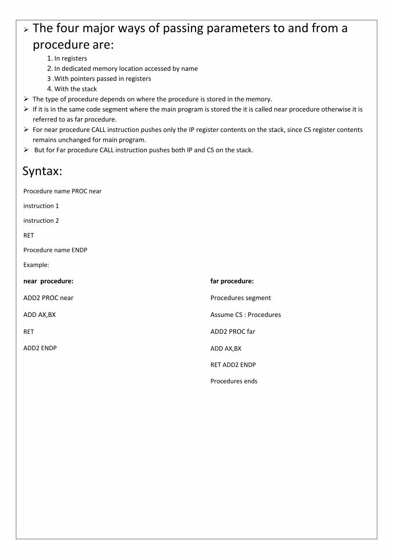
➢ The four major ways of passing parameters to and from a procedure are:
1. In registers
2. In dedicated memory location accessed by name
3 .With pointers passed in registers
4. With the stack
➢ The type of procedure depends on where the procedure is stored in the memory.
➢ If it is in the same code segment where the main program is stored the it is called near procedure otherwise it is
referred to as far procedure.
➢ For near procedure CALL instruction pushes only the IP register contents on the stack, since CS register contents
remains unchanged for main program.
➢ But for Far procedure CALL instruction pushes both IP and CS on the stack.
Syntax:
Procedure name PROC near
instruction 1
instruction 2
RET
Procedure name ENDP
Example:
near procedure:
ADD2 PROC near
ADD AX,BX
RET
ADD2 ENDP
far procedure:
Procedures segment
Assume CS : Procedures
ADD2 PROC far
ADD AX,BX
RET ADD2 ENDP
Procedures ends
159
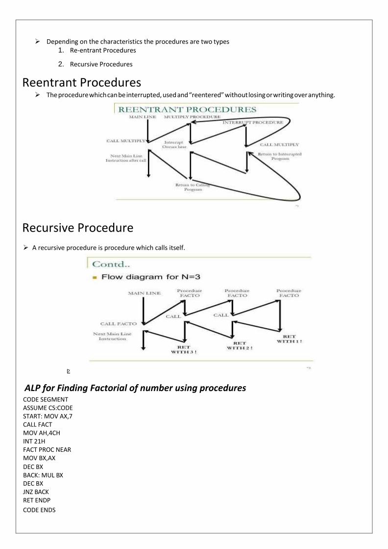
➢ Depending on the characteristics the procedures are two types 1. Re-entrant Procedures
2. Recursive Procedures
Reentrant Procedures ➢ The procedure which can be interrupted, used and “reentered” without losing or writing over anything.
Recursive Procedure
➢ A recursive procedure is procedure which calls itself.
ALP for Finding Factorial of number using procedures CODE SEGMENT ASSUME CS:CODE START: MOV AX,7 CALL FACT MOV AH,4CH INT 21H FACT PROC NEAR MOV BX,AX
DEC BX BACK: MUL BX DEC BX JNZ BACK RET ENDP
CODE ENDS
160
END START
Macros: ➢ A macro is a group of repetitive instructions in a program which are codified only once and can be used as many
times as necessary.
➢ A macro can be defined anywhere in program using the directives MACRO and ENDM
➢ Each time we call the macro in a program, the assembler will insert the defined group of instructions in place of the call.
➢ The assembler generates machine codes for the group of instructions each time the macro is called.
➢ Using a macro avoids the overhead time involved in calling and returning from a procedure. Syntax of macro:
macroname MACRO
instruction1
instruction2
.
.
ENDM
➢ Example:
Read MACRO
mov ah,01h
int 21h ENDM
Display MACRO
mov dl,al
Mov ah,02h
int 21h
ENDM
161
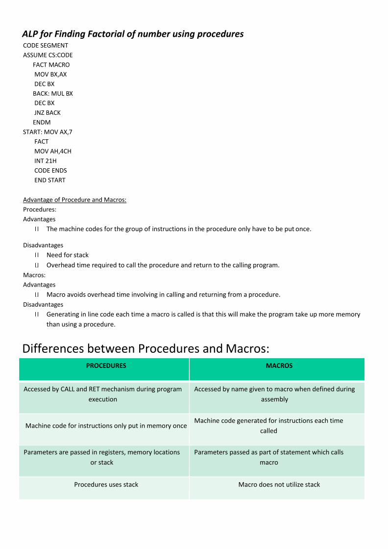
ALP for Finding Factorial of number using procedures CODE SEGMENT
ASSUME CS:CODE
FACT MACRO
MOV BX,AX
DEC BX
BACK: MUL BX
DEC BX
JNZ BACK
ENDM
START: MOV AX,7
FACT
MOV AH,4CH
INT 21H
CODE ENDS
END START
Advantage of Procedure and Macros:
Procedures:
Advantages
The machine codes for the group of instructions in the procedure only have to be put once.
Disadvantages
Need for stack
Overhead time required to call the procedure and return to the calling program.
Macros:
Advantages
Macro avoids overhead time involving in calling and returning from a procedure.
Disadvantages
Generating in line code each time a macro is called is that this will make the program take up more memory
than using a procedure.
Differences between Procedures and Macros:
PROCEDURES MACROS
Accessed by CALL and RET mechanism during program
execution
Accessed by name given to macro when defined during
assembly
Machine code for instructions only put in memory once Machine code generated for instructions each time
called
Parameters are passed in registers, memory locations
or stack
Parameters passed as part of statement which calls
macro
Procedures uses stack Macro does not utilize stack
162
A procedure can be defined anywhere in program using
the directives PROC and ENDP
A macro can be defined anywhere in program using the
directives MACRO and ENDM
Procedures takes huge memory for CALL (3 bytes each
time CALL is used) instruction
Length of code is very huge if macro’s are called for more
number of times
8086 MEMORY INTERFACING:
Most the memory ICs are byte oriented i.e., each memory location can store only one byte of data.
The 8086 is a 16-bit microprocessor, it can transfer 16-bit data.
So in addition to byte, word (16-bit) has to be stored in the memory.
To implement this , the entire memory is divided into two memory banks: Bank0 and Bank1.
Bank0 is selected only when A0 is zero and Bank1 is selected only when BHE’ is zero.
A0 is zero for all even addresses, so Bank0 is usually referred as even addressed memory bank.
BHE’ is used to access higher order memory bank, referred to as odd addressed memory bank.
Every microprocessor based system has a memory system.
Almost all systems contain two basic types of memory, read only memory (ROM) and random access memory
(RAM) or read/write memory.
ROM contains system software and permanent system data such as lookup tables, IVT..etc.
RAM contains temporary data and application software.
ROMs/PROMs/EPROMs are mapped to cover the CPU’s reset address, since these are non-volatile.
163

When the 8086 is reset, the next instruction is fetched from the memory location FFFF0H.
So in the 8086 system the location FFFF0H must be in ROM location.
Address Decoding Techniques
1. Absolute decoding
2. Linear decoding
3. Block decoding
1. Absolute Decoding:
In the absolute decoding technique the memory chip is selected only for the specified logic level on the
address lines: no other logic levels can select the chip.
Below figure the memory interface with absolute decoding. Two 8K EPROMs (2764) are used to provide even
and odd memory banks.
Control signals BHE and A0 are use to enable output of odd and even memory banks respectively. As each
memory chip has 8K memory locations, thirteen address lines are required to address each locations,
independently.
All remaining address lines are used to generate an unique chip select signal. This address technique is
normally used in large memory systems.
Linear Decoding:
In small system hardware for the decoding logic can be eliminated by using only required number of addressing lines (not
all). Other lines are simple ignored. This technique is referred as linear decoding or partial decoding. Control signals BHE
and Ao are used to enable odd and even memory banks, respectively. Figure shows the addressing of 16K RAM (6264) with
linear decoding.
164
The address line A19 is used to select the RAM chips. When A19 is low, chip is selected, otherwise it is disabled. The
status of A14 to A18 does not affect the chip selection logic. This gives you multiple addresses (shadow addresses). This
technique reduces the cost of decoding circuit, but it gas drawback of multiple addresses.
Block Decoding:
In a microcomputer system the memory array is often consists of several blocks of memory chips. Each block of memory
requires decoding circuit. To avoid separate decoding for each memory block special decoder IC is used to generate chip
select signal for each block.
Figure shows the Block decoding technique using 74138, 3:8 decoder
Interfacing RAM, ROM, EPROM to 8086:
➢ The general procedure of static memory interfacing with 8086
165
1. Arrange the available memory chips so as to obtain 16-bit data bus width.
• The upper 8-bit bank is called ‘odd address memory bank’.
• The lower 8-bit bank is called ‘even address memory bank’.
2. Connect available memory address lines of memory chips with those of the microprocessor and also connect
the RD and WR inputs to the corresponding processor control signals.
3. Connect the 16-bit data bus of memory bank with that of the microprocessor 8086.
4. The remaining address lines of the microprocessor, BHE and A0 are used for decoding the required chip select
signals for the odd and even memory banks. The CS of memory is derived from the output of the decoding
circuit.
Problem 1:
Interface two 4Kx8 EPROM and two 4Kx8 RAM chips with 8086. Select suitable maps.
Solution:
We know that, after reset, the IP and CS are initialized to form address FFFF0H. Hence, this address must lie in the EPROM.
The address of RAM may be selected anywhere in the 1MB address space of 8086, but we will select the RAM address such
that the address map of the system is continuous.
Memory Map Table
Addre A1 A1 A1 A1 A1 A1 A1 A1 A1 A1 A0 A0 A0 A0 A0 A0 A0 A0 A0 A0
ss 9 8 7 6 5 4 3 2 1 0 9 8 7 6 5 4 3 2 1 0
FFFFF
H
1 1 1 1 1 1 1 1 1 1 1 1 1 1 1 1 1 1 1 1
EPROM 8K X 8
FE000
H
1 1 1 1 1 1 1 0 0 0 0 0 0 0 0 0 0 0 0 0
FDFFF
H
1 1 1 1 1 1 0 1 1 1 1 1 1 1 1 1 1 1 1 1
RAM 8K X 8
FC000 1 1 1 1 1 1 0 0 0 0 0 0 0 0 0 0 0 0 0 0
H
166
Total 8K bytes of EPROM need 13 address lines A0-A12 (since z13 = 8K).
Address lines A13 - A19 are used for decoding to generate the chip select.
The 𝐵𝐻𝐸 signal goes low when a transfer is at odd address or higher byte of data is to be accessed.
Let us assume that the latched address, 𝐵𝐻𝐸 and demultiplexed data lines are readily available for interfacing.
The memory system in this problem contains in total four 4K x 8 memory chips.
The two 4K x 8 chips of RAM and ROM are arranged in parallel to obtain 16-bit data bus width. If A0 is 0, i.e., the
address is even and is in RAM, then the lower RAM chip is selected indicating 8-bit transfer at an even address. If A0 is
i.e., the address is odd and is in RAM, the 𝐵𝐻𝐸 goes low, the upper RAM chip is selected, further indicating that the 8-
bit transfer is at an odd address. If the selected addresses are in ROM, the respective ROM chips are selected. If at a
time A0 and 𝐵𝐻𝐸 both are 0, both the RAM or ROM chips are selected, i.e., the data transfer is of 16 bits. The
selection of chips here takes place as shown in table below.
167

Memory Chip Selection Table:
Decoder I/P -->
Address/𝐵𝐻𝐸 -->
A2
A13
A1
A0
A0
𝐵𝐻𝐸
Selection/
Comment
Word transfer on D0 - D15 0 0 0 Even and odd address in RAM
Byte transfer on D7 - D0 0 0 1 Only even address in RAM
Byte transfer on D8 - D15 0 1 0 Only odd address in RAM
Word transfer on D0 - D15 1 0 0 Even and odd address in RAM
Byte transfer on D7 - D0 1 0 1 Only even address in RAM
Byte transfer on D8 - D15 1 1 0 Only odd address in ROM
Problem2: Design an interface between 8086 CPU and two chips of 16K×8 EPROM and two chips of 32K×8
RAM. Select the starting address of EPROM suitably. The RAM address must start at 00000 H.
Solution: The last address in the map of 8086 is FFFFF H. after resetting, the processor starts from FFFF0 H. hence this
address must lie in the address range of EPROM.
168
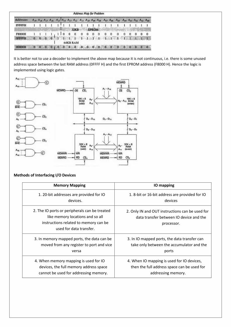
It is better not to use a decoder to implement the above map because it is not continuous, i.e. there is some unused
address space between the last RAM address (0FFFF H) and the first EPROM address (F8000 H). Hence the logic is
implemented using logic gates.
Methods of Interfacing I/O Devices
Memory Mapping IO mapping
1. 20-bit addresses are provided for IO
devices.
1. 8-bit or 16-bit address are provided for IO
devices
2. The IO ports or peripherals can be treated
like memory locations and so all
instructions related to memory can be
used for data transfer.
2. Only IN and OUT instructions can be used for
data transfer between IO device and the
processor.
3. In memory mapped ports, the data can be
moved from any register to port and vice
versa
3. In IO mapped ports, the data transfer can
take only between the accumulator and the
ports
4. When memory mapping is used for IO
devices, the full memory address space
cannot be used for addressing memory.
4. When IO mapping is used for IO devices,
then the full address space can be used for
addressing memory.
169

TEXT / REFERENCE BOOKS
1. Ramesh Goankar, "Microprocessor architecture programming and applications with 8085 / 8088", 5th Edition, Penram International Publishing. 2. A.K.Ray and Bhurchandi, "Advanced Microprocessor", 1st Edition, TMH Publication. 3. Doughlas V.Hall, "Microprocessors and Digital system", 2nd Editon, Mc Graw Hill,1983. 4. Md.Rafiquzzaman, "Microprocessors and Microcomputer based system design", 2nd Editon,Universal Book
Stall, 1992.
Question Bank PART-A
1. What are the different types of addressing modes of 8086 instruction set?
2. What are the different types of instructions in 8086 microprocessor?
3. How many data lines and address lines are available in 8086?
4. What are the 8086 interrupt types?
5. Calculate the physical address for fetching the next instruction to be executed, in 8086?
6. List the flags of 8086.
7. Give any four pin definitions for the minimum mode.
8. What is the operation of S0, S1 and S2 pins in maximum mode?
9. Give the register classification of 8086.
10. What is pipelining?
11. What are the two parts of a flag register?
12. What happens when a high is applied to RESET pin?
13. Explain the BHE and LOCK signals of 8086
14. What are the differences between maximum mode and minimum mode
PART- B 1. Explain the architecture of 8086
2. Explain briefly about the internal hardware architecture of 8086 microprocessor with a neat diagram
3. A) Explain the Data transfer, arithmetic and branch instructions with examples (B) Write an 8086 ALP to
find the sum of numbers in an array of 10 element.
4. (a) Draw and explain the maximum mode of 8086. (b) List the advantages of multiprocessor system
5. Explain the bus interface unit and execution unit of 8086 microprocessor.
6. Explain in detail about the system bus timing of 8086.
170

171

SCHOOL OF ELECTRICAL AND ELECTRONICS
DEPARTMENT OF COMPUTER SCIENCE ENGINEERING
UNIT – V - MICROCONTROLLER– SECA1404
172
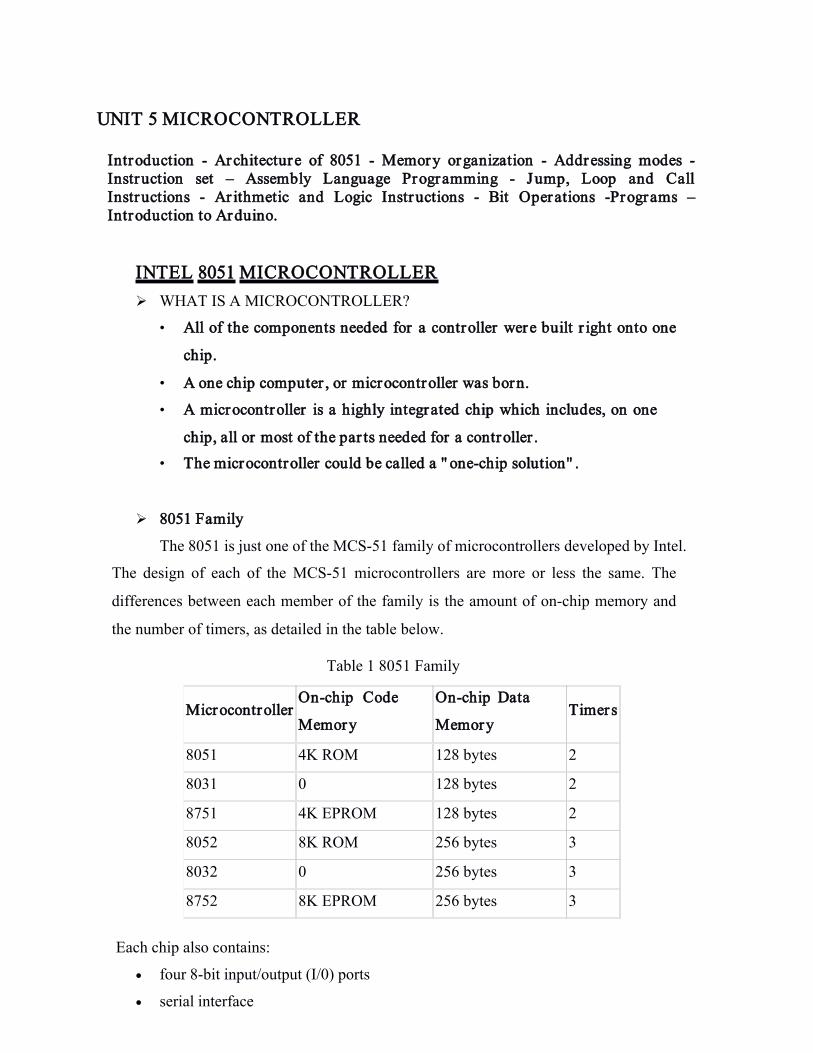
UNIT 5 MICROCONTROLLER
Introduction - Architecture of 8051 - Memory organization - Addressing modes -Instruction set – Assembly Language Programming - Jump, Loop and CallInstructions - Ar ithmetic and Logic Instructions - Bit Operations -Programs –Introduction to Arduino.
INTEL 8051 MICROCONTROLLER WHAT IS A MICROCONTROLLER?
• All of the components needed for a controller were built r ight onto one
chip.
• A one chip computer , or microcontroller was born.
• A microcontroller is a highly integrated chip which includes, on one
chip, all or most of the par ts needed for a controller .• The microcontroller could be called a " one-chip solution" .
8051 Family
The 8051 is just one of the MCS-51 family of microcontrollers developed by Intel.
The design of each of the MCS-51 microcontrollers are more or less the same. The
differences between each member of the family is the amount of on-chip memory and
the number of timers, as detailed in the table below.
Table 1 8051 Family
MicrocontrollerOn-chip Code
Memory
On-chip Data
MemoryTimers
8051 4K ROM 128 bytes 2
8031 0 128 bytes 2
8751 4K EPROM 128 bytes 2
8052 8K ROM 256 bytes 3
8032 0 256 bytes 3
8752 8K EPROM 256 bytes 3
Each chip also contains:
four 8-bit input/output (I/0) ports
serial interface173
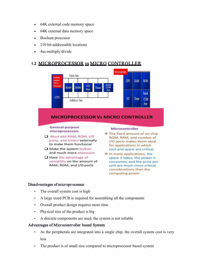
64K external code memory space
64K external data memory space
Boolean processor
210 bit-addressable locations
4us multiply/divide
1.2 MICROPROCESSOR vs MICRO CONTROLLER
Disadvantages of microprocessor
• The overall system cost is high
• A large sized PCB is required for assembling all the components
• Overall product design requires more time
• Physical size of the product is big
• A discrete components are used, the system is not reliable
Advantages of Microcontroller based System
• As the peripherals are integrated into a single chip, the overall system cost is very
less
• The product is of small size compared to microprocessor based system
174
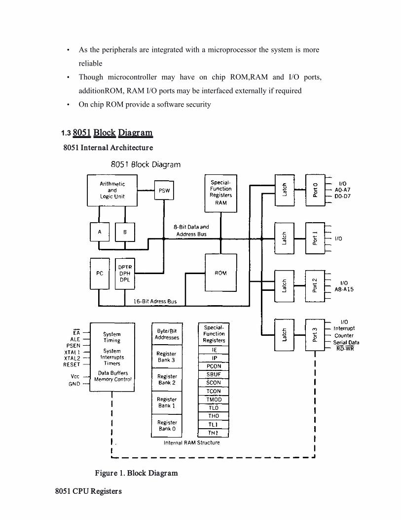
• As the peripherals are integrated with a microprocessor the system is more
reliable
• Though microcontroller may have on chip ROM,RAM and I/O ports,
additionROM, RAM I/O ports may be interfaced externally if required
• On chip ROM provide a software security
1.3 8051 Block Diagram8051 Internal Architecture
Figure 1. Block Diagram
8051 CPU Registers
175
• ACCUMULATOR ( ACC )
• Operandregister
• Implicit or specified in the instruction
• Has an address in on chip SFR bank
• B REGISTER
• to store one of the operands for multiplication and division
• otherwise, scratch pad
• considered as a SFR
• PROGRAM STATUS WORD ( PSW )
• Set of flags contain status information
• One of the SFR
• STACK POINTER ( SP )
• 8 bit wide register
• Incremented before data is stored on to the stack using PUSH or
CALL instructions
• Stack defined anywhere on the 128 byte RAM
• RESET initiated to 0007H
• Not a top to down structure
• Allotted an address in SFR
• DATA POINTER ( DPTR )
• 16 bit register
• contains DPH and DPL
• Pointer to external RAM address
• DPH and DPL allotted separate addresses in SFR bank
• PORT 0 TO 3 LATCHES & DRIVERS
• Each i/o port allotted a latch and a driver
• Latches allotted address in SFR
• User can communicate via these ports
• P0, P1, P2,P3
• SERIAL DATA BUFFER
• internally had TWO independent registers
• TRANSMIT bufferparallel in serial out ( PISO )
• RECEIVE buffer serial in parallel out (SIPO)
• identified by SBUF and allotted an address in SFR
176
• byte written to SBUF initiates serial TX
• byte read from SBUF reads serially received data
• TIMER REGISTERS
• for Timer0 ( 16 bit register – TL0 & TH0 )
• for Timer1 ( 16 bit register – TL1 & TH1 )
• four addresses allotted in SFR
• CONTROL REGISTERS
• IP
• IE
• TMOD
• TCON
• SCON
• PCON
• contain control and status information for interrupts,
timers/counters and serial port
• Allotted separate address in SFR
• TIMING AND CONTROL UNIT
• derives necessary timing and control signals
For internal circuit and external system bus
• OSCILLATOR
• generates basic timing clock signal using crystal oscillator
• INSTRUCTION REGISTER
• decodes the opcode and gives information to timing and control
unit
• EPROM & PROGRAM ADDRESS REGISTER
• provide on chip EPROM and mechanism to address it
• All versions don’t have EPROM
• RAM & RAM ADDRESS REGISTER
• provide internal 128 bytes RAM and a mechanism to address
internally• ALU
• Performs 8 bit arithmetic and logical operations over the operands
held by TEMP1 and TEMP 2
• User cannot access temporary registers
177
• SFR REGISTER BANK
• set of special function registers
• address range : 80 H to FF H
– Interrupt, serial port and timer units control and perform specific
functions under the control of timing and control unit
1.4 Addressing Modes
The five addressing modes are:
Immediate
Register
Direct
Indirect
Indexed
Immediate Addressing
If the operand is a constant then it can be stored in memory immediately after the
opcode. Remember, values in code memory (ROM) do not change once the system has
been programmed and is in use in the everyday world. Therefore, immediate addressing is
only of use when the data to be read is a constant.
For example, if your program needed to perform some calculations based on the number
of weeks in the year, you could use immediate addressing to load the number 52 (34H)
into a register and then perform arithmetic operations upon this data.
MOV R0, #34
The above instruction is an example of immediate addressing. It moves the data
34H into R0. The assembler must be able to tell the difference between an address anda
piece of data. The has symbol (#) is used for this purpose (whenever the assembler sees #
before a number it knows this is immediate addressing). This is a two-byte instruction.Register Addressing
Often we need to move data from a register into the accumulator so that we can
perform arithmetic operations upon it. For example, we may wish to move the contents of
R5 into the accumulator.
MOV A, R5
178
This is an example of register addressing. It moves data from R5 (in the currently
selected register bank) into the accumulator.
ADD A, R6
The above is another example of register addressing. It adds the contents of R6 to the
accumulator, storing the result in the accumulator. Note that in both examples the
destination comes first. This is true of all instructions.Direct Addressing
Direct addressing is used for accessing data in the on-chip RAM. Since there are
256 bytes of RAM (128 bytes general storage for the programmer and another 128 bytes
for the SFRs). That means the addresses go from 00H to FFH, any of which can be stored
in an 8-bit location.
MOV A, 67
The above instruction moves the data in location 67H into the accumulator. Note the
difference between this and immediate addressing. Immediate addressing uses the data,
which is immediately after the instruction. With direct addressing, the operand is an
address. The data to be operated upon is stored in that address. The assembler realises this
is an address and not data because there is no hash symbol before it.ADD A, 06
The above instruction adds the contents of location 06H to the accumulator and stores
the result in the accumulator. If the selected register bank is bank 0 then this instruction
is the same as ADD A, R6.
Indirect Addressing
Register addressing and direct addressing both restrict the programmer to
manipulation of data in fixed addresses. The address the instruction reads from (MOV A,
30H) or writes to (MOV 30H, A) cannot be altered while the program is running. There
are times when it is necessary to read and write to a number of contiguous memory
locations. For example, if you had an array of 8-bit numbers stored in memory, starting at
address 30H, you may wish to examine the contents of each number in the array(perhaps
to find the smallest number). To do so, you would need to read location 30H, then 31H,
then 32H and so on. This can be achieved using indirect addressing. R0 and R1 may be
used as pointer registers. We can use either one to store the current memory location and
then use the indirect addressing instruction shown below.
MOV A, @Ri
179
whereRi is either R0 or R1. Now, we can read the contents of location 30H through
indirect addressing:
MOV R0,
#30H MOV A,
@R0
The first instruction is an example of immediate addressing whereby the data 30H is
placed in R0. The second instruction is indirect addressing. It moves the contents of
location 30H into the accumulator.If we now wish to get the data in location 31H we use the following:
INC R0
MOV A,
@R0
Once we see how to write a loop in assembly language, we will be able to read theentire
contents of the array.
Index Addressing Mode & On-chip ROM Access
• Limitation of register indirect addressing:
• 8-bit addresses (internal RAM)
• DPTR: 16 bits
• MOVC A, @A+DPTR ; “C” means program (code) space ROM
1.5 Special Function Registers (SFRs)
Locations 80H to FFH contain the special function registers. As you can see from
the diagram above, not all locations are used by the 8051 (eleven locations are blank).
These extra locations are used by other family members (8052, etc.) for the extra features
these microcontrollers possess. Also note that not all SFRs are bit- addressable. Those
that are have a unique address for each bit. We will deal with each of the SFRs as we
progress through the course, but for the moment you should take noteof the accumulator
(ACC) at address E0H and the four port registers at addresses 80Hfor P0, 90h for P1,
A0 for P2 and B0 for P3. We will later see how easy this makes ready from and
writing to any of the four ports. Program Status Word (PSW)
The PSW is at location D0H and is bit addressable. The table below describes thefunction180
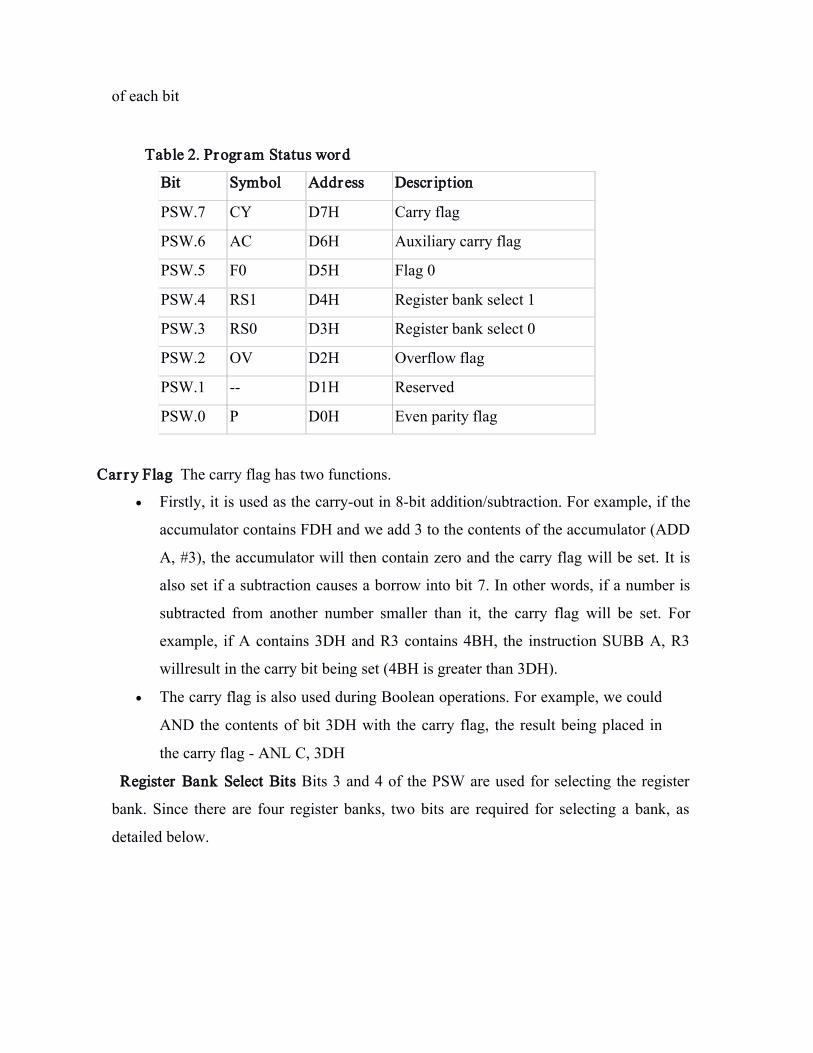
of each bit
Table 2. Program Status word
Carry Flag The carry flag has two functions.
Firstly, it is used as the carry-out in 8-bit addition/subtraction. For example, if the
accumulator contains FDH and we add 3 to the contents of the accumulator (ADD
A, #3), the accumulator will then contain zero and the carry flag will be set. It is
also set if a subtraction causes a borrow into bit 7. In other words, if a number is
subtracted from another number smaller than it, the carry flag will be set. For
example, if A contains 3DH and R3 contains 4BH, the instruction SUBB A, R3
willresult in the carry bit being set (4BH is greater than 3DH).
The carry flag is also used during Boolean operations. For example, we could
AND the contents of bit 3DH with the carry flag, the result being placed in
the carry flag - ANL C, 3DH
Register Bank Select Bits Bits 3 and 4 of the PSW are used for selecting the register
bank. Since there are four register banks, two bits are required for selecting a bank, as
detailed below.
Bit Symbol Address Descr iption
PSW.7 CY D7H Carry flag
PSW.6 AC D6H Auxiliary carry flag
PSW.5 F0 D5H Flag 0
PSW.4 RS1 D4H Register bank select 1
PSW.3 RS0 D3H Register bank select 0
PSW.2 OV D2H Overflow flag
PSW.1 -- D1H Reserved
PSW.0 P D0H Even parity flag
181
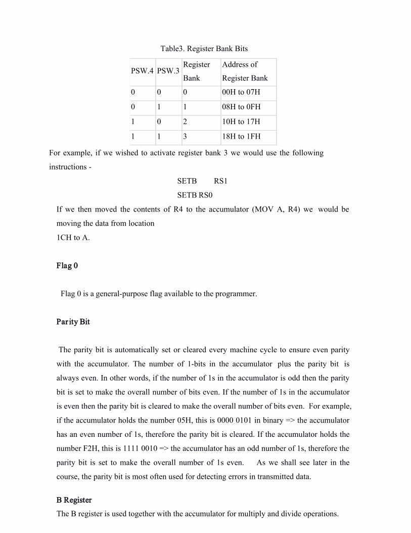
Table3. Register Bank Bits
PSW.4 PSW.3Register
Bank
Address of
Register Bank
0 0 0 00H to 07H
0 1 1 08H to 0FH
1 0 2 10H to 17H
1 1 3 18H to 1FH
For example, if we wished to activate register bank 3 we would use the following
instructions -
SETB RS1
SETB RS0
If we then moved the contents of R4 to the accumulator (MOV A, R4) we would be
moving the data from location
1CH to A.
Flag 0
Flag 0 is a general-purpose flag available to the programmer.
Par ity Bit
The parity bit is automatically set or cleared every machine cycle to ensure even parity
with the accumulator. The number of 1-bits in the accumulator plus the parity bit is
always even. In other words, if the number of 1s in the accumulator is odd then the parity
bit is set to make the overall number of bits even. If the number of 1s in the accumulator
is even then the parity bit is cleared to make the overall number of bits even. For example,
if the accumulator holds the number 05H, this is 0000 0101 in binary => the accumulator
has an even number of 1s, therefore the parity bit is cleared. If the accumulator holds the
number F2H, this is 1111 0010 => the accumulator has an odd number of 1s, therefore the
parity bit is set to make the overall number of 1s even. As we shall see later in the
course, the parity bit is most often used for detecting errors in transmitted data.
B Register
The B register is used together with the accumulator for multiply and divide operations.182
The MUL AB instruction multiplies the values in A and B and stores the low-
byteof the result in A and the high-byte in B.
o For example, if the accumulator contains F5H and the B register contains
02H, the result of MUL AB will be A = EAH and B = 01H.
The DIV AB instruction divides A by B leaving the integer result in A and
theremainder by B.
183
o For example, if the accumulator contains 07H and the B register contains
02H, the result of DIV AB will be A = 03H and B = 01H.
The B register is also bit-addressable.
Stack Pointer
The stack pointer (SP) is an 8-bit register at location 81H. A stack is used for
temporarily storing data. It operates on the basis of last in first out (LIFO). Putting data
onto the stack is called "pushing onto the stack" while taking data off the stack is called
"popping the stack." The stack pointer contains the address of the item currently on top
of the stack. On power-up or reset the SP is set to 07H. When pushing data onto the stack,
the SP is first increased by one and the data is then placed in the location pointed to by the
SP. When popping the stack, the data is taken off the stack and the SP is then decreased
by one. Since reset initialises the SP to 07H, the first item pushed onto the stack is stored
at 08H (remember, the SP is incremented first, then the item is placed on the stack).
However, if the programmer wishes to use the register banks 1 to 3, which start at address
08H, he/she must move the stack to another part of memory. The general purpose RAM
starting at address 30H is a good spot to place the stack. To do so we need to change the
contents of the SP.
MOV SP, #2FH.
Now, the first item to be pushed onto the stack will be stored at 30H.
Subroutines and the Stack
We have already looked at calling a subroutine in the previous section. Now we will
look at the actual call instructions and the effect they have on the stack.ACALL and LCALL
ACALL stands for absolute call while LCALL stands for long call. These
two instructions allow the programmer to call a subroutine. There is a slight difference
between the two instructions, the same as the difference between AJMP and LJMP.
ACALL allows you to jump to a subroutine within the same 2K page while LCALL
allows you to jump to a subroutine anywhere in the 64K code space. The advantage of
ACALLover LCALL is that it is a 2-byte instruction while LCALL is a 3-byte instruction.184
Help from the Assembler
In the same way that you, the programmer, may use the assembler instruction
JMP anytime you need an unconditional jump and the assembler will replace this with
the appropriate 8051 jump instruction (SJMP, AJMP or LJMP), you may use the
assembler CALL instruction and it will be replaced by the appropriate 8051 subroutine
call instruction (ACALL or LCALL - note there is no SCALL instruction).LCALL Operation
Since the ACALL and LCALL instructions perform almost the same functions we
will look at the operation of the LCALL instruction only.
LCALL add16 - long call to subroutine
Encoding - 0001 0010 aaaaaaaaaaaaaaaa (3-byte instruction)
Operation -
(PC) <- (PC) + 3
(SP) <- (SP) + 1
((SP)) <- (PC7-PC0)
(SP) <- (SP) + 1
((SP)) <- (PC15 - PC8)
(PC) <- add15 - add0
The operation is as follows. The PC is increased by 3 (because this is a 3-byte
instruction). The stack pointer is incremented so that it points to the next empty space on
the stack. The third line reads: the contents of the contents of the SP get the low byte of
the PC. On system reset the SP is initialised with the value 07H. Therefore, the first item
pushed onto the stack will be stored in location 08H. Therefore:
((SP)) is equivalent to (08) - meaning location 08H in memory gets the low bye of the PC
- ((SP)) <- (PC7 - PC0)
After the low byte of the PC has been stored on the stack the SP is incremented to pointto
the next empty space on the stack (ie; the SP now contains 09H).
185
SP)) is now equivalent to (09) - meaning location 09H in memory gets the high bye of the
PC - ((SP)) <- (PC15 - PC8)
Now that the PC has been stored on the stack the PC is loaded with the 16-bit
address (add15 - add0). Subroutines are generally sections of code that will be used many
times by the system. A subroutine might be used for taking information from a keyboard
or writing data to a serial link. A particular subroutine will be stored at some point in code
memory, but it can be called from any location in the program. Therefore, the system
needs some way of knowing where to jump back to once execution of the subroutine is
complete. The first diagram below shows the contents of the PC and the SP as the
instruction LCALL sub (at location 103BH in code memory) is about to be executed.
Notice the SP is at its reset value of 07H and the PC contains the address of the next
instruction to be executed
RET
A subroutine must end with the RET instruction, which simply means return from
subroutine. Since a subroutine can be called from anywhere in code memory, the RET
instruction does not specify where to return to. The return address may be different each
time the subroutine is called. If you take the flashing LED program from the last section,
we called twoLoopDelay in the main program after we had turned on the LED. But we
also called twoLoopDelay from within threeLoopDelay. In these two calls the return
address is different; in the first call we are returning to the main program once
twoLoopDelay has completed, but on the second call we are returning to threeLoopDelay.
The system knows where to return to because, as we have seen above, the return address
(ie; the address of the next instruction after the LCALL) is stored on the stack. Therefore,the operation of the RET instruction is:
RET - return from
subroutine Encoding - 0010
0010 Operation -
(PC15 - PC8) <- ((SP))
(SP) <- (SP) - 1
(PC7 - PC0) <- ((SP))
(SP) <- (SP) - 1
186
If you look at the diagram above, note the SP contains 09H - it's pointing at the high-byte
of the return address. Therefore, the contents of location 09H are placed in the high-byte
of the PC (PC15 - PC8).
The SP is then decremented (it now contains 08H) so that it points at the low-byte of the
return address. So, the contents of location 08H are placed in the low-byte of the PC (PC7
- PC0).
In our example above, the PC will now contain 103EH, and execution takes up
immediately after the LCALL sub instruction. Also note that the stack is now empty - SP
contains 07H.
II INSTRUCTION SET (8051)
2.1 Introduction
The process of writing program for the microcontroller mainly consists of giving
instructions (commands) in the specific order in which they should be executed in order
to carry out a specific task. As electronics cannot “understand” what for example an
instruction “if the push button is pressed- turn the light on” means, then a certain number
of simpler and precisely defined orders that decoder can recognise must be used. All
commands are known as INSTRUCTION SET.
All microcontrollers compatibile with the 8051 have in total of 255 instructions,
i.e. 255 different words available for program writing. At first sight, it is imposing
number of odd signs that must be known by heart. However, It is not so complicated as it
looks like. Many instructions are considered to be “different”, even though they perform
the same operation, so there are only 111 truly different commands.
For example: ADD A,R0, ADD A,R1, ... ADD A,R7 are instructions that
perform the same operation (additon of the accumulator and register). Since there are 8
such registers, each instruction is counted separately. Taking into account that all
instructions perform only 53 operations (addition, subtraction, copy etc.) and most of
them are rarely used in practice, there are actually 20-30 abbreviations to be learned,
which is acceptable.
2.2 Types of instructions187
Depending on operation they perform, all instructions are divided in several groups:
• Arithmetic Instructions
• Branch Instructions
• Data Transfer Instructions
• Logic Instructions
• Bit-oriented Instructions
The first part of each instruction, called MNEMONIC refers to the operation an
instruction performs (copy, addition, logic operation etc.). Mnemonics are abbreviations
of the name of operation being executed. For example:
• INC R1 - Means: Increment register R1 (increment register R1);
• JNZ LOOP - Means: Jump if Not Zero LOOP (if the number in the accumulator is not 0,
jump to the address marked as LOOP);
The other part of instruction, called OPERAND is separated from mnemonic by at
least one whitespace and defines data being processed by instructions. Some of the
instructions have no operand, while some of them have one, two or three. If there is
more than one operand in an instruction, they are separated by a comma. For example:• RET - return from a subroutine;
• JZ TEMP - if the number in the accumulator is not 0, jump to the address marked as
TEMP;
• ADD A, R3 - add R3 and accumulator;
• CJNE A, #20,LOOP - compare accumulator with 20. If they are not equal, jump to
theaddress marked as LOOP;
2.2.1 Arithmetic instructions
Arithmetic instructions perform several basic operations such as addition, subtraction,
division, multiplication etc. After execution, the result is stored in the first operand.
For example:
ADD A,R1 - The result of addition (A+R1) will be stored in the accumulator.
ADD A,Rn Adds the register to the accumulator
ADD A,direct Adds the direct byte to the accumulator
ADD A,@Ri Adds the indirect RAM to the accumulator
ADD A,#data Adds the immediate data to the accumulator188
ADDC A,Rn Adds the register to the accumulator with a carry flag
ADDC A,direct Adds the direct byte to the accumulator with a carry flag
ADDC A,@Ri Adds the indirect RAM to the accumulator with a carry
flag
ADDC A,#data Adds the immediate data to the accumulator with a carry
flagSUBB A,Rn Subtracts the register from the accumulator with a borrow
SUBB A,direct Subtracts the direct byte from the accumulator with a borrow
SUBB A,@Ri Subtracts the indirect RAM from the accumulator with a borrow
SUBB A,#data Subtracts the immediate data from the accumulator with a borrow
INC A Increments the accumulator by 1
INC Rn Increments the register by 1
INC Rx Increments the direct byte by 1
INC @Ri Increments the indirect RAM by
1DEC A Decrements the accumulator by 1
DEC Rn Decrements the register by 1
DEC Rx Decrements the direct byte by 1
DEC @Ri Decrements the indirect RAM by
1INC DPTR Increments the Data Pointer by
1 MUL AB Multiplies A and B 1
DIV AB Divides A by B 1
DA A Decimal adjustment of the accumulator according to BCD code
2.2.2 Branch Instructions
There are two kinds of branch instructions:
Unconditional jump instructions: upon their execution a jump to a new
locationfrom where the program continues execution is executed.
Conditional jump instructions: a jump to a new program location is executed only
if a specified condition is met.
Otherwise, the program normally proceeds with the next instruction.
ACALL addr11 Absolute subroutine
call LCALL addr16 Long subroutine
call RET Returns from subroutine
RETI Returns from interrupt subroutineAJMP addr11 Absolute
189
SJMP rel Short jump (from –128 to +127 locations relative to the following
instruction)
JC rel Jump if carry flag is set. Short jump.
JNC rel Jump if carry flag is not set. Short jump.
JB bit,rel Jump if direct bit is set. Short jump.
JBC bit,rel Jump if direct bit is set and clears bit. Short jump.
JMP @A+DPTR Jump indirect relative to the DPTR
JZ rel Jump if the accumulator is zero. Short jump.
JNZ rel Jump if the accumulator is not zero. Short jump.
CJNE A,direct,rel Compares direct byte to the accumulator and jumps if notequal.
Short jump.
CJNE A,#data,rel Compares immediate data to the accumulator and jumps if notequal.
Short jump.
CJNE Rn,#data,rel Compares immediate data to the register and jumps if notequal.
Short jump.
CJNE @Ri,#data,rel Compares immediate data to indirect register and jumps ifnot
equal. Short jump.
DJNZ Rn,rel Decrements register and jumps if not 0. Short jump.
DJNZ Rx,rel Decrements direct byte and jump if not 0. Short jump.
NOP No operation
2.2.3 Data Transfer Instructions
Data transfer instructions move the content of one register to another. The register the
content of which is moved remains unchanged. If they have the suffix “X” (MOVX),the
data is exchanged with external memory.
MOV A,Rn Moves the register to the accumulator MOV A,direct Moves the direct
byte to the accumulator
MOV A,@Ri Moves the indirect RAM to the accumulator
MOV A,#data Moves the immediate data to the accumulator
MOV Rn,A Moves the accumulator to the register
MOV Rn,direct Moves the direct byte to the register
MOV Rn,#data Moves the immediate data to the register
MOV direct,A Moves the accumulator to the direct byte190
MOV direct,Rn Moves the register to the direct byte
MOV direct,direct Moves the direct byte to the direct
byte
MOV direct,@Ri Moves the indirect RAM to the direct byte
MOV direct,#data Moves the immediate data to the direct byte
MOV @Ri,A Moves the accumulator to the indirect RAM
MOV @Ri,direct Moves the direct byte to the indirect RAM
MOV @Ri,#data Moves the immediate data to the indirect
RAMMOV DPTR,#data Moves a 16-bit data to the data pointer
MOVC A,@A+DPTR Moves the code byte relative to the DPTR to the
accumulator(address=A+DPTR)
MOVC A,@A+PC Moves the code byte relative to the PC to the accumulator
(address=A+PC)
MOVX A,@Ri Moves the external RAM (8-bit address) to the accumulator
MOVX A,@DPTR Moves the external RAM (16-bit address) to the
accumulatorMOVX @Ri,A Moves the accumulator to the external RAM (8-bit
address) MOVX @DPTR,A Moves the accumulator to the external RAM (16-
bit address)PUSH direct Pushes the direct byte onto the stackPOP direct Pops the direct byte from the stack
XCH A,Rn Exchanges the register with the accumulator
XCH A,direct Exchanges the direct byte with the accumulator
XCH A,@Ri Exchanges the indirect RAM with the
accumulator
XCHD A,@Ri Exchanges the low-order nibble indirect RAM with the accumulator
2.2.4 Logic Instructions
Logic instructions perform logic operations upon corresponding bits of two registers.
After execution, the result is stored
in the first operand.
ANL A,Rn AND register to accumulator
ANL A,direct AND direct byte to accumulator ANL A,@Ri AND indirect RAM to
accumulator
ANL A,#data AND immediate data to accumulatorANL direct,A AND accumulator to
direct byte 191
ANL direct,#data AND immediae data to direct register ORL A,Rn OR register to
accumulator
ORL A,direct OR direct byte to accumulator ORL A,@Ri OR indirect RAM to
accumulatorORL direct,A OR accumulator to direct byte
ORL direct,#data OR immediate data to direct byte
XRL A,Rn Exclusive OR register to accumulator
XRL A,direct Exclusive OR direct byte to accumulator
XRL A,@Ri Exclusive OR indirect RAM to
accumulator
XRL A,#data Exclusive OR immediate data to
accumulator XRL direct,A Exclusive OR accumulator to
direct byte
XORL direct,#data Exclusive OR immediate data to direct byte
CLR A Clears the accumulator
CPL A Complements the accumulator (1=0, 0=1)
SWAP A Swaps nibbles within the accumulator
RL A Rotates bits in the accumulator left
RLC A Rotates bits in the accumulator left through carry
RR A Rotates bits in the accumulator right
RRC A Rotates bits in the accumulator right through carry
2.2.5 Bit-or iented Instructions
Similar to logic instructions, bit-oriented instructions perform logic operations. The
difference is that these are performed
upon single bits.
CLR C Clears the carry flag
CLR bit Clears the direct
bit SETB C Sets the carry
flag SETB bit Sets the
direct bit
CPL C Complements the carry flag
CPL bit Complements the direct
bit
ANL C,bit AND direct bit to the carry flag192
ANL C,/bit AND complements of direct bit to the carry
flagORL C,bit OR direct bit to the carry flag
ORL C,/bit OR complements of direct bit to the carry
flagMOV C,bit Moves the direct bit to the carry flag
MOV bit,C Moves the carry flag to the direct bit
Descr iption of all 8051 instructions
Here is a list of the operands and their meanings:
A - accumulator;
Rn - is one of working registers (R0-R7) in the currently active RAM memory bank;
Direct - is any 8-bit address register of RAM. It can be any general-purpose register or a
SFR (I/O port, control register etc.);@Ri - is indirect internal or external RAM location addressed by register R0 or R1;
#data - is an 8-bit constant included in instruction (0-255);
#data16 - is a 16-bit constant included as bytes 2 and 3 in instruction (0-65535);
addr16 - is a 16-bit address. May be anywhere within 64KB of program memory;
addr11 - is an 11-bit address. May be within the same 2KB page of program memory as
the first byte of the following instruction;
rel - is the address of a close memory location (from -128 to +127 relative to the first byte
of the following instruction). On the basis of it, assembler computes the value to add or
subtract from the number currently stored in the program counter;
bit - is any bit-addressable I/O pin, control or status bit; andC - is carry flag of the status register (register PSW).
8051 Addressing Modes8051 has four addressing modes.1. Immediate Addressing :Data is immediately available in the instruction.For example -
ADD A, #77; Adds 77 (decimal) to A and stores in A
ADD A, #4DH; Adds 4D (hexadecimal) to A and stores in A
MOV DPTR, #1000H; Moves 1000 (hexadecimal) to data
pointer193

2. Bank Addressing or Register Addressing :This way of addressing accesses the bytes in the current register bank. Data is available inthe register specified in the instruction. The register bank is decided by 2 bits of ProcessorStatus Word (PSW).For example-
ADD A, R0; Adds content of R0 to A and stores in A
3.. Direct Addressing :
The address of the data is available in the
instruction. For example -
MOV A, 088H; Moves content of SFR TCON (address 088H)to A
4. Register Indirect Addressing :
The address of data is available in the R0 or R1 registers as specified in the
instruction. For example -
MOV A, @R0 moves content of address pointed by R0 to A
External Data Addressing :
Pointer used for external data addressing can be either R0/R1 (256 byte access) or
DPTR (64kbyte access).
For example -
MOVX A, @R0; Moves content of 8-bit address pointed by R0 to A
MOVX A, @DPTR; Moves content of 16-bit address pointed by DPTR to A
External Code Addressing :
Sometimes we may want to store non-volatile data into the ROM e.g. look-up tables.
Such data may require reading the code memory. This may be done as follows -
MOVC A, @A+DPTR; Moves content of address pointed by A+DPTR to A
MOVC A, @A+PC; Moves content of address pointed by A+PC to A
I/O Por t Configuration
Each port of 8051 has bidirectional capability. Port 0 is called 'true bidirectional port' as it
floats (tristated) when configured as input. Port-1, 2, 3 are called 'quasi bidirectional
port'. Port-0 Pin Structure194
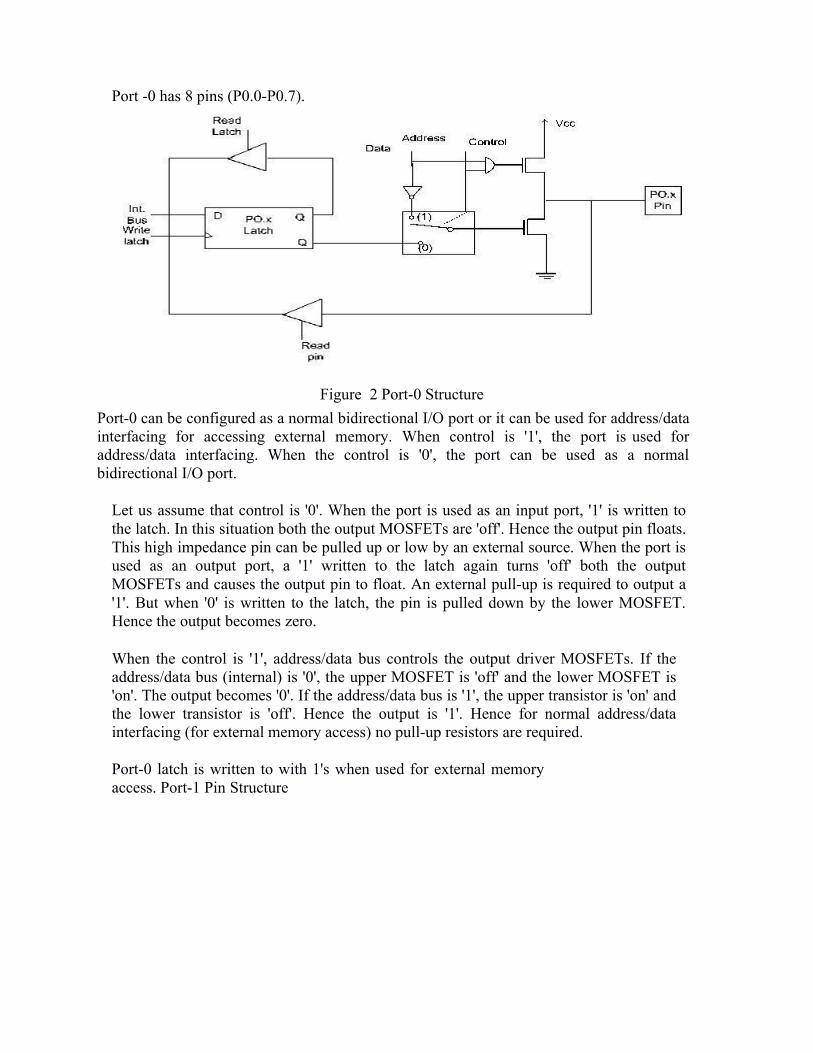
Port -0 has 8 pins (P0.0-P0.7).
Figure 2 Port-0 StructurePort-0 can be configured as a normal bidirectional I/O port or it can be used for address/datainterfacing for accessing external memory. When control is '1', the port is used foraddress/data interfacing. When the control is '0', the port can be used as a normalbidirectional I/O port.
Let us assume that control is '0'. When the port is used as an input port, '1' is written tothe latch. In this situation both the output MOSFETs are 'off'. Hence the output pin floats.This high impedance pin can be pulled up or low by an external source. When the port isused as an output port, a '1' written to the latch again turns 'off' both the outputMOSFETs and causes the output pin to float. An external pull-up is required to output a'1'. But when '0' is written to the latch, the pin is pulled down by the lower MOSFET.Hence the output becomes zero.
When the control is '1', address/data bus controls the output driver MOSFETs. If theaddress/data bus (internal) is '0', the upper MOSFET is 'off' and the lower MOSFET is'on'. The output becomes '0'. If the address/data bus is '1', the upper transistor is 'on' andthe lower transistor is 'off'. Hence the output is '1'. Hence for normal address/datainterfacing (for external memory access) no pull-up resistors are required.
Port-0 latch is written to with 1's when used for external memoryaccess. Port-1 Pin Structure
195
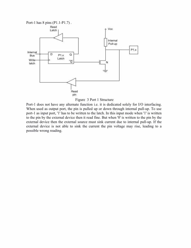
Port-1 has 8 pins (P1.1-P1.7) .
Figure 3 Port 1 StructurePort-1 does not have any alternate function i.e. it is dedicated solely for I/O interfacing.When used as output port, the pin is pulled up or down through internal pull-up. To useport-1 as input port, '1' has to be written to the latch. In this input mode when '1' is writtento the pin by the external device then it read fine. But when '0' is written to the pin by theexternal device then the external source must sink current due to internal pull-up. If theexternal device is not able to sink the current the pin voltage may rise, leading to apossible wrong reading.
196
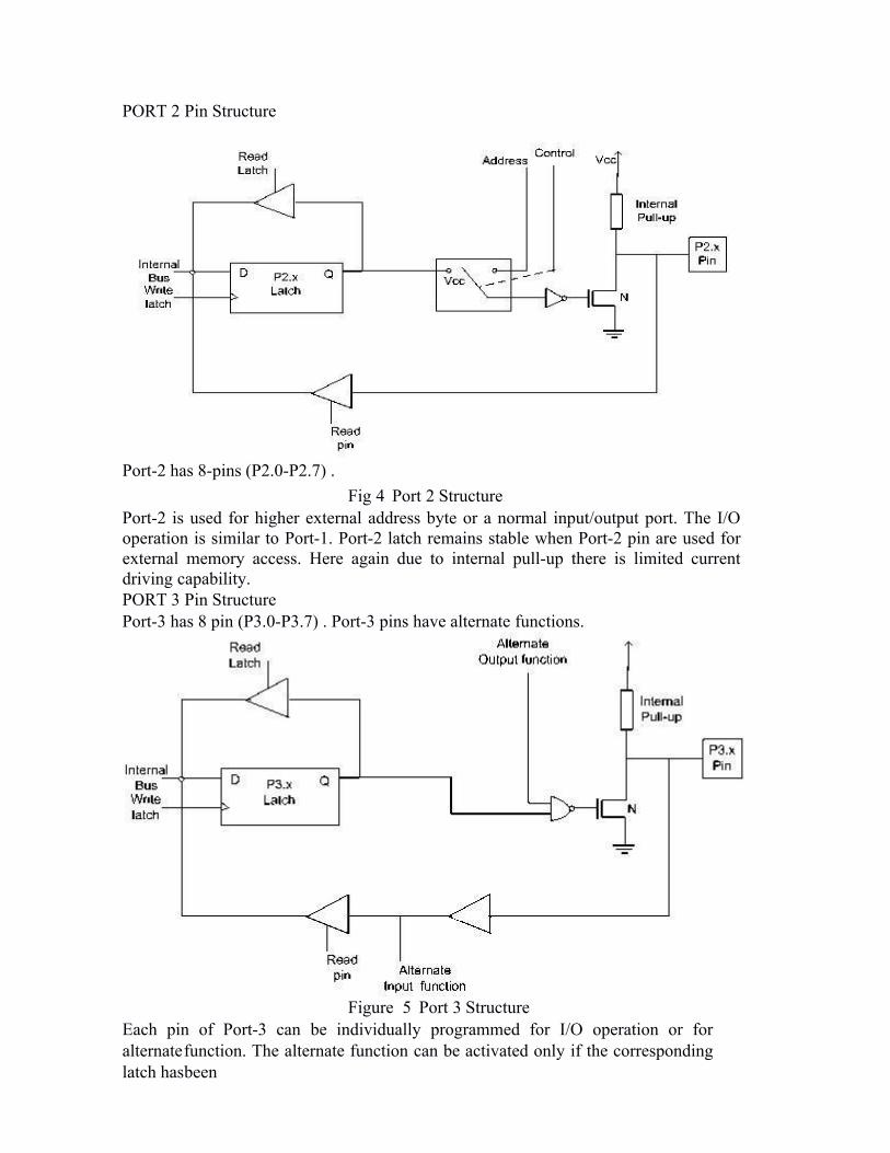
PORT 2 Pin Structure
Port-2 has 8-pins (P2.0-P2.7) .Fig 4 Port 2 Structure
Port-2 is used for higher external address byte or a normal input/output port. The I/Ooperation is similar to Port-1. Port-2 latch remains stable when Port-2 pin are used forexternal memory access. Here again due to internal pull-up there is limited currentdriving capability.PORT 3 Pin StructurePort-3 has 8 pin (P3.0-P3.7) . Port-3 pins have alternate functions.
Figure 5 Port 3 StructureEach pin of Port-3 can be individually programmed for I/O operation or foralternatefunction. The alternate function can be activated only if the correspondinglatch hasbeen
197
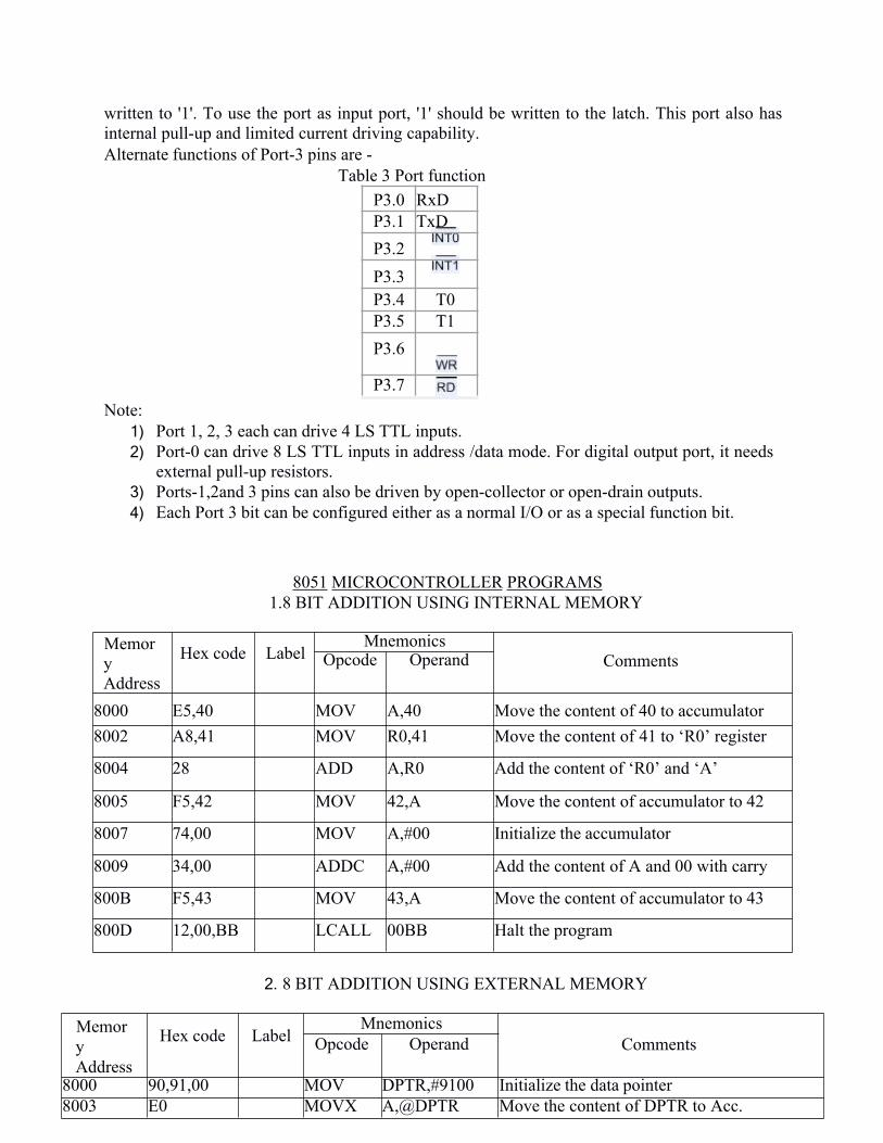
written to '1'. To use the port as input port, '1' should be written to the latch. This port also hasinternal pull-up and limited current driving capability.Alternate functions of Port-3 pins are -
Table 3 Port functionP3.0 RxDP3.1 TxDP3.2P3.3P3.4 T0P3.5 T1P3.6
P3.7Note:
1) Port 1, 2, 3 each can drive 4 LS TTL inputs.2) Port-0 can drive 8 LS TTL inputs in address /data mode. For digital output port, it needs
external pull-up resistors.3) Ports-1,2and 3 pins can also be driven by open-collector or open-drain outputs.4) Each Port 3 bit can be configured either as a normal I/O or as a special function bit.
8051 MICROCONTROLLER PROGRAMS1.8 BIT ADDITION USING INTERNAL MEMORY
MemoryAddress
Hex code LabelMnemonics
CommentsOpcode Operand
8000 E5,40 MOV A,40 Move the content of 40 to accumulator8002 A8,41 MOV R0,41 Move the content of 41 to ‘R0’ register
8004 28 ADD A,R0 Add the content of ‘R0’ and ‘A’
8005 F5,42 MOV 42,A Move the content of accumulator to 42
8007 74,00 MOV A,#00 Initialize the accumulator
8009 34,00 ADDC A,#00 Add the content of A and 00 with carry
800B F5,43 MOV 43,A Move the content of accumulator to 43
800D 12,00,BB LCALL 00BB Halt the program
2. 8 BIT ADDITION USING EXTERNAL MEMORY
MemoryAddress
Hex code LabelMnemonics
CommentsOpcode Operand
8000 90,91,00 MOV DPTR,#9100 Initialize the data pointer8003 E0 MOVX A,@DPTR Move the content of DPTR to Acc.198
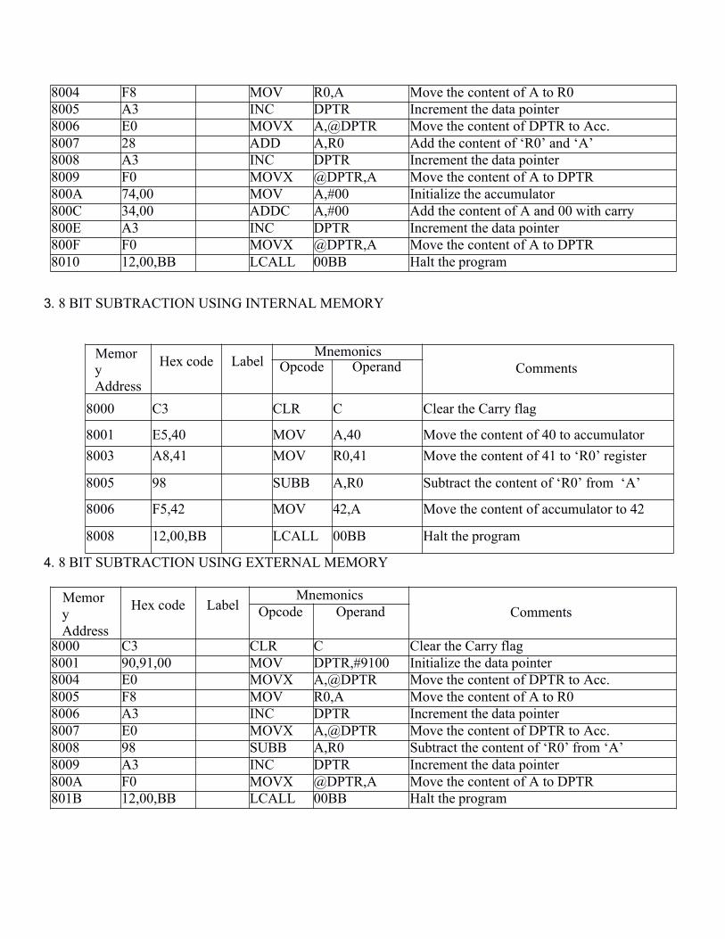
8004 F8 MOV R0,A Move the content of A to R08005 A3 INC DPTR Increment the data pointer8006 E0 MOVX A,@DPTR Move the content of DPTR to Acc.8007 28 ADD A,R0 Add the content of ‘R0’ and ‘A’8008 A3 INC DPTR Increment the data pointer8009 F0 MOVX @DPTR,A Move the content of A to DPTR800A 74,00 MOV A,#00 Initialize the accumulator800C 34,00 ADDC A,#00 Add the content of A and 00 with carry800E A3 INC DPTR Increment the data pointer800F F0 MOVX @DPTR,A Move the content of A to DPTR8010 12,00,BB LCALL 00BB Halt the program
3. 8 BIT SUBTRACTION USING INTERNAL MEMORY
MemoryAddress
Hex code LabelMnemonics
CommentsOpcode Operand
8000 C3 CLR C Clear the Carry flag
8001 E5,40 MOV A,40 Move the content of 40 to accumulator8003 A8,41 MOV R0,41 Move the content of 41 to ‘R0’ register
8005 98 SUBB A,R0 Subtract the content of ‘R0’ from ‘A’
8006 F5,42 MOV 42,A Move the content of accumulator to 42
8008 12,00,BB LCALL 00BB Halt the program
4. 8 BIT SUBTRACTION USING EXTERNAL MEMORY
MemoryAddress
Hex code LabelMnemonics
CommentsOpcode Operand
8000 C3 CLR C Clear the Carry flag8001 90,91,00 MOV DPTR,#9100 Initialize the data pointer8004 E0 MOVX A,@DPTR Move the content of DPTR to Acc.8005 F8 MOV R0,A Move the content of A to R08006 A3 INC DPTR Increment the data pointer8007 E0 MOVX A,@DPTR Move the content of DPTR to Acc.8008 98 SUBB A,R0 Subtract the content of ‘R0’ from ‘A’8009 A3 INC DPTR Increment the data pointer800A F0 MOVX @DPTR,A Move the content of A to DPTR801B 12,00,BB LCALL 00BB Halt the program
199
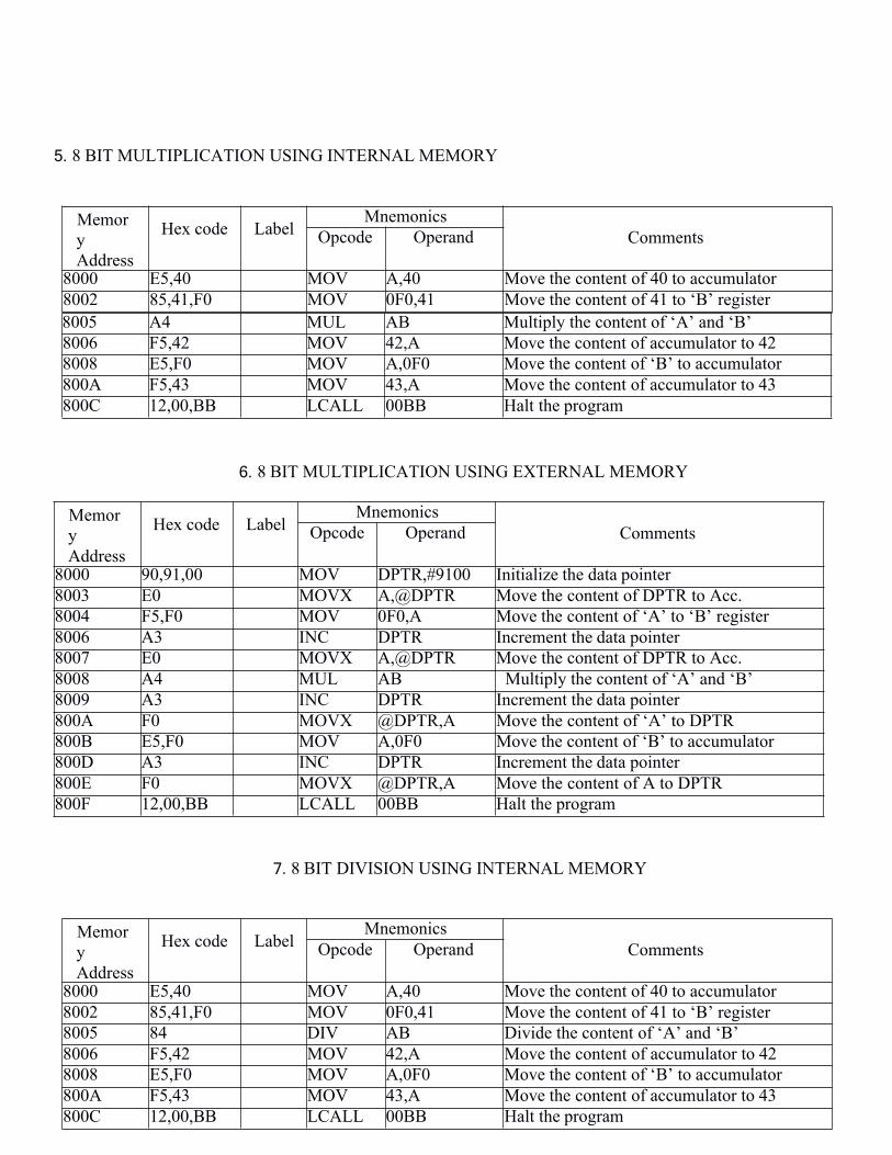
5. 8 BIT MULTIPLICATION USING INTERNAL MEMORY
MemoryAddress
Hex code LabelMnemonics
CommentsOpcode Operand
8000 E5,40 MOV A,40 Move the content of 40 to accumulator8002 85,41,F0 MOV 0F0,41 Move the content of 41 to ‘B’ register
6. 8 BIT MULTIPLICATION USING EXTERNAL MEMORY
MemoryAddress
Hex code LabelMnemonics
CommentsOpcode Operand
8000 90,91,00 MOV DPTR,#9100 Initialize the data pointer8003 E0 MOVX A,@DPTR Move the content of DPTR to Acc.8004 F5,F0 MOV 0F0,A Move the content of ‘A’ to ‘B’ register8006 A3 INC DPTR Increment the data pointer8007 E0 MOVX A,@DPTR Move the content of DPTR to Acc.8008 A4 MUL AB Multiply the content of ‘A’ and ‘B’8009 A3 INC DPTR Increment the data pointer800A F0 MOVX @DPTR,A Move the content of ‘A’ to DPTR800B E5,F0 MOV A,0F0 Move the content of ‘B’ to accumulator800D A3 INC DPTR Increment the data pointer800E F0 MOVX @DPTR,A Move the content of A to DPTR800F 12,00,BB LCALL 00BB Halt the program
7. 8 BIT DIVISION USING INTERNAL MEMORY
MemoryAddress
Hex code LabelMnemonics
CommentsOpcode Operand
8000 E5,40 MOV A,40 Move the content of 40 to accumulator8002 85,41,F0 MOV 0F0,41 Move the content of 41 to ‘B’ register8005 84 DIV AB Divide the content of ‘A’ and ‘B’8006 F5,42 MOV 42,A Move the content of accumulator to 428008 E5,F0 MOV A,0F0 Move the content of ‘B’ to accumulator800A F5,43 MOV 43,A Move the content of accumulator to 43800C 12,00,BB LCALL 00BB Halt the program
8005 A4 MUL AB Multiply the content of ‘A’ and ‘B’8006 F5,42 MOV 42,A Move the content of accumulator to 428008 E5,F0 MOV A,0F0 Move the content of ‘B’ to accumulator800A F5,43 MOV 43,A Move the content of accumulator to 43800C 12,00,BB LCALL 00BB Halt the program
200
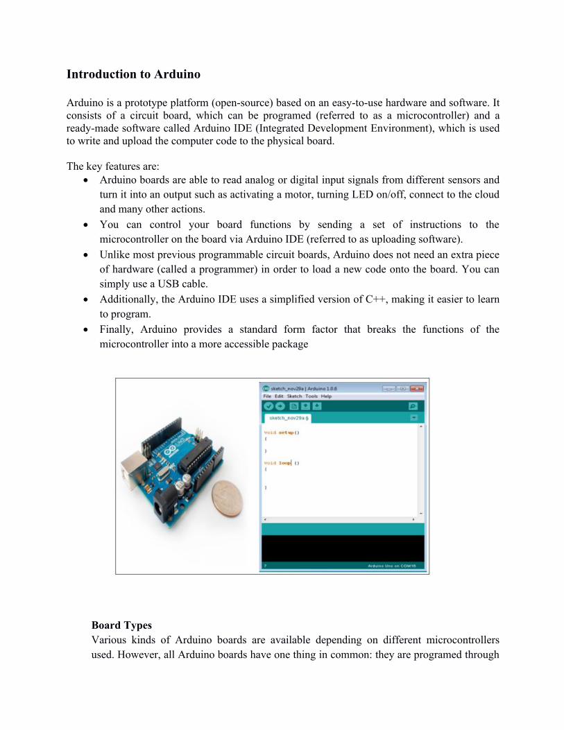
Introduction to Arduino
Arduino is a prototype platform (open-source) based on an easy-to-use hardware and software. Itconsists of a circuit board, which can be programed (referred to as a microcontroller) and aready-made software called Arduino IDE (Integrated Development Environment), which is usedto write and upload the computer code to the physical board.
The key features are: Arduino boards are able to read analog or digital input signals from different sensors and
turn it into an output such as activating a motor, turning LED on/off, connect to the cloudand many other actions.
You can control your board functions by sending a set of instructions to themicrocontroller on the board via Arduino IDE (referred to as uploading software).
Unlike most previous programmable circuit boards, Arduino does not need an extra pieceof hardware (called a programmer) in order to load a new code onto the board. You cansimply use a USB cable.
Additionally, the Arduino IDE uses a simplified version of C++, making it easier to learnto program.
Finally, Arduino provides a standard form factor that breaks the functions of themicrocontroller into a more accessible package
Board TypesVarious kinds of Arduino boards are available depending on different microcontrollersused. However, all Arduino boards have one thing in common: they are programed through
201
the Arduino IDE. The differences are based on the number of inputs and outputs (thenumber of sensors, LEDs, and buttons you can use on a single board), speed, operatingvoltage, form factor etc. Some boards are designed to be embedded and have noprogramming interface (hardware), which you would need to buy separately. Some can rundirectly from a 3.7V battery, others need at least 5V.Here is a list of different Arduino boards available.
202

ARDUINO – BOARD DESCRIPTION
In this chapter, we will learn about the different components on the Arduino board. We willstudy the Arduino UNO board because it is the most popular board in the Arduino boardfamily. In addition, it is the best board to get started with electronics and coding. Someboards look a bit different from the one given below, but most Arduinos have majority ofthese components in common.
Power USBArduino board can be powered by using the USB cable from your computer. Allyou need to do is connect the USB cable to the USB connection (1).
Power (Barrel Jack)Arduino boards can be powered directly from the AC mains power supply byconnecting it to the Barrel Jack (2).
Voltage RegulatorThe function of the voltage regulator is to control the voltage given to theArduino board and stabilize the DC voltages used by the processor and otherelements.
Crystal Oscillator
203
The crystal oscillator helps Arduino in dealing with time issues. How doesArduino calculate time? The answer is, by using the crystal oscillator. Thenumber printed on top of the Arduino crystal is 16.000H9H. It tells us that thefrequency is 16,000,000 Hertz or 16 MHz.
Arduino ResetYou can reset your Arduino board, i.e., start your program from the beginning.You can reset the UNO board in two ways. First, by using the reset button (17)on the board. Second, you can connect an external reset button to the Arduinopin labelled RESET (5).
Pins (3.3, 5, GND, Vin) 3.3V (6): Supply 3.3 output volt 5V (7): Supply 5 output volt Most of the components used with Arduino board works fine with 3.3 volt and 5
volt. GND (8)(Ground): There are several GND pins on the Arduino, any of which can
be used to ground your circuit. Vin (9): This pin also can be used to power the Arduino board from an external
power source, like AC mains power supply
Analog pins
The Arduino UNO board has five analog input pins A0 through A5. These pins canread the signal from an analog sensor like the humidity sensor or temperature sensorand convert it into a digital value that can be read by the microprocessor.
Main microcontroller
Each Arduino board has its own microcontroller (11). You can assume it as the brainof your board. The main IC (integrated circuit) on the Arduino is slightly differentfrom board to board. The microcontrollers are usually of the ATMEL Company. Youmust know what IC your board has before loading up a new program from the ArduinoIDE. This information is available on the top of the IC. For more details about the ICconstruction and functions, you can refer to the data sheet.
ICSP pin
Mostly, ICSP (12) is an AVR, a tiny programming header for the Arduino consistingof MOSI, MISO, SCK, RESET, VCC, and GND. It is often referred to as an SPI(Serial Peripheral Interface), which could be considered as an "expansion" of theoutput. Actually, you are slaving the output device to the master of the SPI bus.
Power LED indicator
This LED should light up when you plug your Arduino into a power source to indicatethat your board is powered up correctly. If this light does not turn on, then there is
204
something wrong with the connection. TX and RX LEDs
On your board, you will find two labels: TX (transmit) and RX (receive). They appearin two places on the Arduino UNO board. First, at the digital pins 0 and 1, to indicatethe pins responsible for serial communication. Second, the TX and RX led (13). TheTX led flashes with different speed while sending the serial data. The speed of flashingdepends on the baud rate used by the board. RX flashes during the receiving process.
Digital I / O
The Arduino UNO board has 14 digital I/O pins (15) (of which 6 provide PWM (PulseWidth Modulation) output. These pins can be configured to work as input digital pinsto read logic 14 values (0 or 1) or as digital output pins to drive different modules likeLEDs, relays, etc. The pins labeled “~” can be used to generate PWM.
AREF
AREF stands for Analog Reference. It is sometimes, used to set an external referencevoltage (between 0 and 5 Volts) as the upper limit for the analog input pins.
TEXT / REFERENCE BOOKS1. Ramesh Goankar, "Microprocessor architecture programming and applications with 8085 /8088", 5th Edition, PenramInternational Publishing.2. A.K.Ray and Bhurchandi, "Advanced Microprocessor", 1st Edition, TMH Publication.3. Kenneth J.Ayala, "The 8051 microcontroller Architecture, Programming and applications"2nd Edition ,Penraminternational.4. Doughlas V.Hall, "Microprocessors and Digital system", 2nd Editon, Mc Graw Hill,1983.5. Md.Rafiquzzaman, "Microprocessors and Microcomputer based system design", 2ndEditon,Universal Book Stall, 1992.6. Hardware Reference Manual for 80X86 family", Intel Corporation, 1990.7. Muhammad Ali Mazidi and Janice Gillispie Mazidi, "The 8051 Microcontroller andEmbedded Systems", 2nd Edition,Pearson.8. “Arduino Made Simple” by Ashwin Pajankar
Question Bank1. Explain the architecture of 8051 microcontroller in detail with the help of neat diagram.2. Gives notes on (a) Instruction format (b) Signed and Unsigned conditional branch instruction.3. Define addressing modes. With suitable examples explain 8051 addressing modes in detail.4. Write a detailed note on assembler dependent instruction and programming
205